WO2021065590A1 - 半導体集積回路装置および半導体集積回路装置の製造方法 - Google Patents
半導体集積回路装置および半導体集積回路装置の製造方法 Download PDFInfo
- Publication number
- WO2021065590A1 WO2021065590A1 PCT/JP2020/035675 JP2020035675W WO2021065590A1 WO 2021065590 A1 WO2021065590 A1 WO 2021065590A1 JP 2020035675 W JP2020035675 W JP 2020035675W WO 2021065590 A1 WO2021065590 A1 WO 2021065590A1
- Authority
- WO
- WIPO (PCT)
- Prior art keywords
- gate wiring
- dummy
- pad
- nanosheet
- semiconductor
- Prior art date
- Legal status (The legal status is an assumption and is not a legal conclusion. Google has not performed a legal analysis and makes no representation as to the accuracy of the status listed.)
- Ceased
Links
Images





Classifications
-
- H—ELECTRICITY
- H10—SEMICONDUCTOR DEVICES; ELECTRIC SOLID-STATE DEVICES NOT OTHERWISE PROVIDED FOR
- H10D—INORGANIC ELECTRIC SEMICONDUCTOR DEVICES
- H10D62/00—Semiconductor bodies, or regions thereof, of devices having potential barriers
- H10D62/10—Shapes, relative sizes or dispositions of the regions of the semiconductor bodies; Shapes of the semiconductor bodies
- H10D62/117—Shapes of semiconductor bodies
- H10D62/118—Nanostructure semiconductor bodies
- H10D62/119—Nanowire, nanosheet or nanotube semiconductor bodies
- H10D62/121—Nanowire, nanosheet or nanotube semiconductor bodies oriented parallel to substrates
-
- H—ELECTRICITY
- H10—SEMICONDUCTOR DEVICES; ELECTRIC SOLID-STATE DEVICES NOT OTHERWISE PROVIDED FOR
- H10D—INORGANIC ELECTRIC SEMICONDUCTOR DEVICES
- H10D84/00—Integrated devices formed in or on semiconductor substrates that comprise only semiconducting layers, e.g. on Si wafers or on GaAs-on-Si wafers
- H10D84/80—Integrated devices formed in or on semiconductor substrates that comprise only semiconducting layers, e.g. on Si wafers or on GaAs-on-Si wafers characterised by the integration of at least one component covered by groups H10D12/00 or H10D30/00, e.g. integration of IGFETs
- H10D84/82—Integrated devices formed in or on semiconductor substrates that comprise only semiconducting layers, e.g. on Si wafers or on GaAs-on-Si wafers characterised by the integration of at least one component covered by groups H10D12/00 or H10D30/00, e.g. integration of IGFETs of only field-effect components
- H10D84/83—Integrated devices formed in or on semiconductor substrates that comprise only semiconducting layers, e.g. on Si wafers or on GaAs-on-Si wafers characterised by the integration of at least one component covered by groups H10D12/00 or H10D30/00, e.g. integration of IGFETs of only field-effect components of only insulated-gate FETs [IGFET]
-
- H—ELECTRICITY
- H10—SEMICONDUCTOR DEVICES; ELECTRIC SOLID-STATE DEVICES NOT OTHERWISE PROVIDED FOR
- H10D—INORGANIC ELECTRIC SEMICONDUCTOR DEVICES
- H10D84/00—Integrated devices formed in or on semiconductor substrates that comprise only semiconducting layers, e.g. on Si wafers or on GaAs-on-Si wafers
- H10D84/80—Integrated devices formed in or on semiconductor substrates that comprise only semiconducting layers, e.g. on Si wafers or on GaAs-on-Si wafers characterised by the integration of at least one component covered by groups H10D12/00 or H10D30/00, e.g. integration of IGFETs
- H10D84/82—Integrated devices formed in or on semiconductor substrates that comprise only semiconducting layers, e.g. on Si wafers or on GaAs-on-Si wafers characterised by the integration of at least one component covered by groups H10D12/00 or H10D30/00, e.g. integration of IGFETs of only field-effect components
- H10D84/83—Integrated devices formed in or on semiconductor substrates that comprise only semiconducting layers, e.g. on Si wafers or on GaAs-on-Si wafers characterised by the integration of at least one component covered by groups H10D12/00 or H10D30/00, e.g. integration of IGFETs of only field-effect components of only insulated-gate FETs [IGFET]
- H10D84/85—Complementary IGFETs, e.g. CMOS
- H10D84/853—Complementary IGFETs, e.g. CMOS comprising FinFETs
-
- B—PERFORMING OPERATIONS; TRANSPORTING
- B82—NANOTECHNOLOGY
- B82Y—SPECIFIC USES OR APPLICATIONS OF NANOSTRUCTURES; MEASUREMENT OR ANALYSIS OF NANOSTRUCTURES; MANUFACTURE OR TREATMENT OF NANOSTRUCTURES
- B82Y10/00—Nanotechnology for information processing, storage or transmission, e.g. quantum computing or single electron logic
-
- B—PERFORMING OPERATIONS; TRANSPORTING
- B82—NANOTECHNOLOGY
- B82Y—SPECIFIC USES OR APPLICATIONS OF NANOSTRUCTURES; MEASUREMENT OR ANALYSIS OF NANOSTRUCTURES; MANUFACTURE OR TREATMENT OF NANOSTRUCTURES
- B82Y40/00—Manufacture or treatment of nanostructures
-
- H—ELECTRICITY
- H10—SEMICONDUCTOR DEVICES; ELECTRIC SOLID-STATE DEVICES NOT OTHERWISE PROVIDED FOR
- H10D—INORGANIC ELECTRIC SEMICONDUCTOR DEVICES
- H10D30/00—Field-effect transistors [FET]
- H10D30/01—Manufacture or treatment
- H10D30/014—Manufacture or treatment of FETs having zero-dimensional [0D] or one-dimensional [1D] channels, e.g. quantum wire FETs, single-electron transistors [SET] or Coulomb blockade transistors
-
- H—ELECTRICITY
- H10—SEMICONDUCTOR DEVICES; ELECTRIC SOLID-STATE DEVICES NOT OTHERWISE PROVIDED FOR
- H10D—INORGANIC ELECTRIC SEMICONDUCTOR DEVICES
- H10D30/00—Field-effect transistors [FET]
- H10D30/60—Insulated-gate field-effect transistors [IGFET]
- H10D30/67—Thin-film transistors [TFT]
- H10D30/6729—Thin-film transistors [TFT] characterised by the electrodes
- H10D30/673—Thin-film transistors [TFT] characterised by the electrodes characterised by the shapes, relative sizes or dispositions of the gate electrodes
- H10D30/6735—Thin-film transistors [TFT] characterised by the electrodes characterised by the shapes, relative sizes or dispositions of the gate electrodes having gates fully surrounding the channels, e.g. gate-all-around
-
- H—ELECTRICITY
- H10—SEMICONDUCTOR DEVICES; ELECTRIC SOLID-STATE DEVICES NOT OTHERWISE PROVIDED FOR
- H10D—INORGANIC ELECTRIC SEMICONDUCTOR DEVICES
- H10D62/00—Semiconductor bodies, or regions thereof, of devices having potential barriers
- H10D62/10—Shapes, relative sizes or dispositions of the regions of the semiconductor bodies; Shapes of the semiconductor bodies
- H10D62/117—Shapes of semiconductor bodies
- H10D62/118—Nanostructure semiconductor bodies
-
- H—ELECTRICITY
- H10—SEMICONDUCTOR DEVICES; ELECTRIC SOLID-STATE DEVICES NOT OTHERWISE PROVIDED FOR
- H10D—INORGANIC ELECTRIC SEMICONDUCTOR DEVICES
- H10D64/00—Electrodes of devices having potential barriers
- H10D64/20—Electrodes characterised by their shapes, relative sizes or dispositions
- H10D64/27—Electrodes not carrying the current to be rectified, amplified, oscillated or switched, e.g. gates
- H10D64/311—Gate electrodes for field-effect devices
- H10D64/411—Gate electrodes for field-effect devices for FETs
- H10D64/511—Gate electrodes for field-effect devices for FETs for IGFETs
- H10D64/512—Disposition of the gate electrodes, e.g. buried gates
-
- H—ELECTRICITY
- H10—SEMICONDUCTOR DEVICES; ELECTRIC SOLID-STATE DEVICES NOT OTHERWISE PROVIDED FOR
- H10D—INORGANIC ELECTRIC SEMICONDUCTOR DEVICES
- H10D84/00—Integrated devices formed in or on semiconductor substrates that comprise only semiconducting layers, e.g. on Si wafers or on GaAs-on-Si wafers
- H10D84/01—Manufacture or treatment
- H10D84/0123—Integrating together multiple components covered by H10D12/00 or H10D30/00, e.g. integrating multiple IGBTs
- H10D84/0126—Integrating together multiple components covered by H10D12/00 or H10D30/00, e.g. integrating multiple IGBTs the components including insulated gates, e.g. IGFETs
- H10D84/0128—Manufacturing their channels
-
- H—ELECTRICITY
- H10—SEMICONDUCTOR DEVICES; ELECTRIC SOLID-STATE DEVICES NOT OTHERWISE PROVIDED FOR
- H10D—INORGANIC ELECTRIC SEMICONDUCTOR DEVICES
- H10D84/00—Integrated devices formed in or on semiconductor substrates that comprise only semiconducting layers, e.g. on Si wafers or on GaAs-on-Si wafers
- H10D84/01—Manufacture or treatment
- H10D84/0123—Integrating together multiple components covered by H10D12/00 or H10D30/00, e.g. integrating multiple IGBTs
- H10D84/0126—Integrating together multiple components covered by H10D12/00 or H10D30/00, e.g. integrating multiple IGBTs the components including insulated gates, e.g. IGFETs
- H10D84/0135—Manufacturing their gate conductors
-
- H—ELECTRICITY
- H10—SEMICONDUCTOR DEVICES; ELECTRIC SOLID-STATE DEVICES NOT OTHERWISE PROVIDED FOR
- H10D—INORGANIC ELECTRIC SEMICONDUCTOR DEVICES
- H10D84/00—Integrated devices formed in or on semiconductor substrates that comprise only semiconducting layers, e.g. on Si wafers or on GaAs-on-Si wafers
- H10D84/01—Manufacture or treatment
- H10D84/0123—Integrating together multiple components covered by H10D12/00 or H10D30/00, e.g. integrating multiple IGBTs
- H10D84/0126—Integrating together multiple components covered by H10D12/00 or H10D30/00, e.g. integrating multiple IGBTs the components including insulated gates, e.g. IGFETs
- H10D84/0165—Integrating together multiple components covered by H10D12/00 or H10D30/00, e.g. integrating multiple IGBTs the components including insulated gates, e.g. IGFETs the components including complementary IGFETs, e.g. CMOS devices
- H10D84/0167—Manufacturing their channels
-
- H—ELECTRICITY
- H10—SEMICONDUCTOR DEVICES; ELECTRIC SOLID-STATE DEVICES NOT OTHERWISE PROVIDED FOR
- H10D—INORGANIC ELECTRIC SEMICONDUCTOR DEVICES
- H10D84/00—Integrated devices formed in or on semiconductor substrates that comprise only semiconducting layers, e.g. on Si wafers or on GaAs-on-Si wafers
- H10D84/01—Manufacture or treatment
- H10D84/0123—Integrating together multiple components covered by H10D12/00 or H10D30/00, e.g. integrating multiple IGBTs
- H10D84/0126—Integrating together multiple components covered by H10D12/00 or H10D30/00, e.g. integrating multiple IGBTs the components including insulated gates, e.g. IGFETs
- H10D84/0165—Integrating together multiple components covered by H10D12/00 or H10D30/00, e.g. integrating multiple IGBTs the components including insulated gates, e.g. IGFETs the components including complementary IGFETs, e.g. CMOS devices
- H10D84/0172—Manufacturing their gate conductors
-
- H—ELECTRICITY
- H10—SEMICONDUCTOR DEVICES; ELECTRIC SOLID-STATE DEVICES NOT OTHERWISE PROVIDED FOR
- H10D—INORGANIC ELECTRIC SEMICONDUCTOR DEVICES
- H10D84/00—Integrated devices formed in or on semiconductor substrates that comprise only semiconducting layers, e.g. on Si wafers or on GaAs-on-Si wafers
- H10D84/01—Manufacture or treatment
- H10D84/0123—Integrating together multiple components covered by H10D12/00 or H10D30/00, e.g. integrating multiple IGBTs
- H10D84/0126—Integrating together multiple components covered by H10D12/00 or H10D30/00, e.g. integrating multiple IGBTs the components including insulated gates, e.g. IGFETs
- H10D84/0165—Integrating together multiple components covered by H10D12/00 or H10D30/00, e.g. integrating multiple IGBTs the components including insulated gates, e.g. IGFETs the components including complementary IGFETs, e.g. CMOS devices
- H10D84/0193—Integrating together multiple components covered by H10D12/00 or H10D30/00, e.g. integrating multiple IGBTs the components including insulated gates, e.g. IGFETs the components including complementary IGFETs, e.g. CMOS devices the components including FinFETs
-
- H—ELECTRICITY
- H10—SEMICONDUCTOR DEVICES; ELECTRIC SOLID-STATE DEVICES NOT OTHERWISE PROVIDED FOR
- H10D—INORGANIC ELECTRIC SEMICONDUCTOR DEVICES
- H10D84/00—Integrated devices formed in or on semiconductor substrates that comprise only semiconducting layers, e.g. on Si wafers or on GaAs-on-Si wafers
- H10D84/01—Manufacture or treatment
- H10D84/02—Manufacture or treatment characterised by using material-based technologies
- H10D84/03—Manufacture or treatment characterised by using material-based technologies using Group IV technology, e.g. silicon technology or silicon-carbide [SiC] technology
- H10D84/038—Manufacture or treatment characterised by using material-based technologies using Group IV technology, e.g. silicon technology or silicon-carbide [SiC] technology using silicon technology, e.g. SiGe
-
- H—ELECTRICITY
- H10—SEMICONDUCTOR DEVICES; ELECTRIC SOLID-STATE DEVICES NOT OTHERWISE PROVIDED FOR
- H10D—INORGANIC ELECTRIC SEMICONDUCTOR DEVICES
- H10D84/00—Integrated devices formed in or on semiconductor substrates that comprise only semiconducting layers, e.g. on Si wafers or on GaAs-on-Si wafers
- H10D84/80—Integrated devices formed in or on semiconductor substrates that comprise only semiconducting layers, e.g. on Si wafers or on GaAs-on-Si wafers characterised by the integration of at least one component covered by groups H10D12/00 or H10D30/00, e.g. integration of IGFETs
- H10D84/82—Integrated devices formed in or on semiconductor substrates that comprise only semiconducting layers, e.g. on Si wafers or on GaAs-on-Si wafers characterised by the integration of at least one component covered by groups H10D12/00 or H10D30/00, e.g. integration of IGFETs of only field-effect components
- H10D84/83—Integrated devices formed in or on semiconductor substrates that comprise only semiconducting layers, e.g. on Si wafers or on GaAs-on-Si wafers characterised by the integration of at least one component covered by groups H10D12/00 or H10D30/00, e.g. integration of IGFETs of only field-effect components of only insulated-gate FETs [IGFET]
- H10D84/85—Complementary IGFETs, e.g. CMOS
-
- H—ELECTRICITY
- H10—SEMICONDUCTOR DEVICES; ELECTRIC SOLID-STATE DEVICES NOT OTHERWISE PROVIDED FOR
- H10D—INORGANIC ELECTRIC SEMICONDUCTOR DEVICES
- H10D89/00—Aspects of integrated devices not covered by groups H10D84/00 - H10D88/00
- H10D89/10—Integrated device layouts
-
- H—ELECTRICITY
- H10—SEMICONDUCTOR DEVICES; ELECTRIC SOLID-STATE DEVICES NOT OTHERWISE PROVIDED FOR
- H10D—INORGANIC ELECTRIC SEMICONDUCTOR DEVICES
- H10D30/00—Field-effect transistors [FET]
- H10D30/40—FETs having zero-dimensional [0D], one-dimensional [1D] or two-dimensional [2D] charge carrier gas channels
- H10D30/43—FETs having zero-dimensional [0D], one-dimensional [1D] or two-dimensional [2D] charge carrier gas channels having one-dimensional [1D] charge carrier gas channels, e.g. quantum wire FETs or transistors having 1D quantum-confined channels
-
- H—ELECTRICITY
- H10—SEMICONDUCTOR DEVICES; ELECTRIC SOLID-STATE DEVICES NOT OTHERWISE PROVIDED FOR
- H10D—INORGANIC ELECTRIC SEMICONDUCTOR DEVICES
- H10D30/00—Field-effect transistors [FET]
- H10D30/60—Insulated-gate field-effect transistors [IGFET]
- H10D30/67—Thin-film transistors [TFT]
- H10D30/6757—Thin-film transistors [TFT] characterised by the structure of the channel, e.g. transverse or longitudinal shape or doping profile
-
- H—ELECTRICITY
- H10—SEMICONDUCTOR DEVICES; ELECTRIC SOLID-STATE DEVICES NOT OTHERWISE PROVIDED FOR
- H10D—INORGANIC ELECTRIC SEMICONDUCTOR DEVICES
- H10D62/00—Semiconductor bodies, or regions thereof, of devices having potential barriers
- H10D62/10—Shapes, relative sizes or dispositions of the regions of the semiconductor bodies; Shapes of the semiconductor bodies
- H10D62/13—Semiconductor regions connected to electrodes carrying current to be rectified, amplified or switched, e.g. source or drain regions
- H10D62/149—Source or drain regions of field-effect devices
- H10D62/151—Source or drain regions of field-effect devices of IGFETs
-
- H—ELECTRICITY
- H10—SEMICONDUCTOR DEVICES; ELECTRIC SOLID-STATE DEVICES NOT OTHERWISE PROVIDED FOR
- H10D—INORGANIC ELECTRIC SEMICONDUCTOR DEVICES
- H10D84/00—Integrated devices formed in or on semiconductor substrates that comprise only semiconducting layers, e.g. on Si wafers or on GaAs-on-Si wafers
- H10D84/01—Manufacture or treatment
- H10D84/0123—Integrating together multiple components covered by H10D12/00 or H10D30/00, e.g. integrating multiple IGBTs
- H10D84/0126—Integrating together multiple components covered by H10D12/00 or H10D30/00, e.g. integrating multiple IGBTs the components including insulated gates, e.g. IGFETs
- H10D84/0165—Integrating together multiple components covered by H10D12/00 or H10D30/00, e.g. integrating multiple IGBTs the components including insulated gates, e.g. IGFETs the components including complementary IGFETs, e.g. CMOS devices
- H10D84/0186—Manufacturing their interconnections or electrodes, e.g. source or drain electrodes
Definitions
- the present disclosure relates to a layout structure of a semiconductor integrated circuit device provided with a standard cell (hereinafter, also simply referred to as a cell as appropriate) using a nanosheet FET (Field Effect Transistor) and a method for manufacturing the same.
- a standard cell hereinafter, also simply referred to as a cell as appropriate
- a nanosheet FET Field Effect Transistor
- first and second standard cells are arranged adjacent to each other in the first direction, the area of the semiconductor integrated circuit device can be reduced.
- the semiconductor layer portion formed at both ends of the nanosheet and forming the terminal serving as the source or drain of the transistor is referred to as a "pad".
- a plurality of standard cells are arranged side by side in the X direction to form a cell row.
- the filler cell CF is arranged between the standard cells C1.
- the standard cell C1 arranged on the left side of the drawing may be referred to as a standard cell C1a, and the standard cell C1 arranged on the right side of the drawing may be referred to as a standard cell C1b.
- the standard cell C1 and the filler cell CF are formed with an N-well region 1 extending in the X and Y directions from the central portion in the Y direction to the upper end of the drawing. Further, the standard cell C1 and the filler cell CF are provided with power supply wirings 11 and 12 extending in the X direction at both ends in the Y direction, respectively. Both the power supply wirings 11 and 12 are embedded power supply wirings (BPR: Buried Power Rail) formed in the embedded wiring layer.
- the power supply wiring 11 is formed in the N-well region 1 and supplies the power supply voltage VDD.
- the power supply wiring 12 supplies the power supply voltage VSS.
- sheet-shaped nanosheets 21 to 24 and dummy nanosheets 31 to 34 spreading in the X and Y directions are formed in layers above the power supply wirings 11 and 12.
- the nanosheets 21 and 22 and the dummy nanosheets 31 and 32 are formed so as to be arranged in the X direction.
- the nanosheets 23 and 24 and the dummy nanosheets 33 and 34 are formed so as to be aligned in the X direction.
- the transistor P1 is composed of the nanosheet 21, the pads 41, 42, and the gate wiring 51.
- Transistors P2 are composed of nanosheets 22, pads 42, 43, and gate wiring 52.
- Transistors N1 are composed of nanosheets 23, pads 44, 45, and gate wiring 51.
- Transistors N2 are composed of nanosheets 24, pads 45, 46, and gate wiring 52.
- local wirings 61 to 65 extending in the Y direction are formed on the upper layers of the pads 41 to 46.
- the local wiring 61 is connected to the pad 41.
- the local wiring 62 is connected to the pad 42.
- the local wiring 63 is connected to the pads 43 and 46.
- the local wiring 64 is connected to the pad 44.
- the local wiring 65 is connected to the pad 45.
- silicon (Si) is used as the material of the semiconductor layer 210
- silicon germanium alloy (SiGe) is used as the material of the sacrificial semiconductor layer 220.
- the laminated structure of the laminated semiconductor 200 can be realized by alternately laminating silicon (Si) and a silicon germanium alloy (SiGe) on the semiconductor substrate 100 by epitaxial growth.
- Epitaxial growth includes rapid thermal chemical vapor deposition (RTCVD), low-energy plasma deposition (LEPD), ultra-high vacuum chemical vapor deposition (UHVCVD), and atmospheric pressure. It is realized by methods such as chemical vapor deposition (APCVD) and molecular beam epitaxy (MBE).
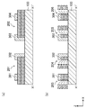
- sacrificial gate structures 301 to 304 are formed on the semiconductor substrate 100 and above the laminated semiconductor portions 201 and 202. Specifically, the sacrificial gate structures 301 to 304 are formed at the formation positions of the gate wiring 52, the dummy gate wirings 56, 57, and the gate wiring 53 in FIG. 1, respectively. Further, the sacrificial gate structures 302 and 303 are formed so as to cover the side surface of the laminated semiconductor portion 201 on the right side of the drawing and the side surface of the laminated semiconductor portion 202 on the left side of the drawing.
- the sacrificial gate structures 301 to 304 include, for example, chemical vapor deposition (CVD), plasma chemical vapor deposition (PECVD), physical vapor deposition (PVD), and physical vapor deposition (PVD).
- CVD chemical vapor deposition
- PECVD plasma chemical vapor deposition
- PVD physical vapor deposition
- PVD physical vapor deposition
- PVD physical vapor deposition
- the film is formed by a method such as sputtering or atomic layer deposition (ALD). Then, the sacrificial gate structures 301 to 304 are formed at predetermined positions by well-known lithography and etching.
- an insulating film 401 as a spacer is formed on the semiconductor substrate 100 on the semiconductor substrate 100.
- the insulating film 401 is formed so as to cover the upper surface of the semiconductor substrate 100 which is not covered by the sacrificial gate structures 301 to 304 and the laminated semiconductor portions 203 to 206.
- the material of the insulating film 401 for example, silicon oxide, silicon nitride, or the like is used.
- the insulating film 401 can be formed by a well-known film formation and etching.
- a semiconductor material to which impurities have been added is used for the epitaxial growth performed to form the pads 501 to 504.
- the semiconductor material for example, silicon is used.
- impurities (semiconductors) added to semiconductor materials for example, boron, aluminum, gallium, indium and the like are used in the case of P-type semiconductors, and antimony, arsenic and phosphorus and the like are used in the case of N-type semiconductors. Be done.
- transistors N2 and N3 near the boundary between the adjacent standard cells C1a and C1b and the filler cell CF are formed.
- wiring such as vias and local wiring is formed on the upper layer of the transistor by a well-known technique, and the connection between the transistors is made.
- the standard cell C1b is formed so as to be adjacent to the gate wiring 53 and the gate wiring 53 on the left side (standard cell C1a side) of the drawing in the X direction of the gate wiring 53 and adjacent to the dummy gate wiring 56.
- the dummy gate wiring 57 and the pad 49 provided between the dummy gate wiring 57 and the gate wiring 53 are provided.
- the dummy nanosheets 31a and 33a are formed so as not to be electrically connected to the dummy nanosheets arranged so as to overlap the dummy gate wiring 55a of the standard cell arranged on the left side of the drawing of the standard cell C3a, respectively. Has been done.
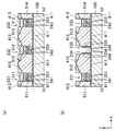
- FIGS. 10 to 13 show X2-X2'cross sections of FIG.
- the side surfaces of the laminated semiconductor portions 231 to 233 are exposed on both the left and right sides of the drawing, respectively.
- the semiconductor layers included in the laminated semiconductor portions 231 to 233 are referred to as semiconductor layers 241 to 243, respectively.
- the sacrificial semiconductor layers included in the laminated semiconductor portions 231 to 233 are referred to as sacrificial semiconductor layers 251 to 253.
- the pad 511 is formed on the left side of the drawing of the laminated semiconductor portion 231 with the exposed portion (side surface on the left side of the drawing) of the laminated semiconductor portion 231 as a base point.
- the pad 512 is formed between the laminated semiconductor portions 231 and 232 with the exposed portion of the laminated semiconductor portion 231 (side surface on the right side of the drawing) and the exposed portion of the laminated semiconductor portion 232 (side surface on the left side of the drawing) as base points.
- the pad 513 is formed between the laminated semiconductor portions 232 and 233 with the exposed portion of the laminated semiconductor portion 232 (side surface on the right side of the drawing) and the exposed portion of the laminated semiconductor portion 233 (side surface on the left side of the drawing) as base points.
- the pad 514 is formed on the right side of the drawing of the laminated semiconductor portion 233 with the exposed portion (the side surface on the right side of the drawing) of the laminated semiconductor portion 233 as a base point.
Landscapes
- Engineering & Computer Science (AREA)
- Chemical & Material Sciences (AREA)
- Nanotechnology (AREA)
- Crystallography & Structural Chemistry (AREA)
- Physics & Mathematics (AREA)
- General Physics & Mathematics (AREA)
- Manufacturing & Machinery (AREA)
- Condensed Matter Physics & Semiconductors (AREA)
- Mathematical Physics (AREA)
- Theoretical Computer Science (AREA)
- Semiconductor Integrated Circuits (AREA)
- Design And Manufacture Of Integrated Circuits (AREA)
- Metal-Oxide And Bipolar Metal-Oxide Semiconductor Integrated Circuits (AREA)
Priority Applications (4)
| Application Number | Priority Date | Filing Date | Title |
|---|---|---|---|
| JP2021550640A JP7598029B2 (ja) | 2019-10-02 | 2020-09-23 | 半導体集積回路装置および半導体集積回路装置の製造方法 |
| CN202080069062.1A CN114467175B (zh) | 2019-10-02 | 2020-09-23 | 半导体集成电路装置及半导体集成电路装置的制造方法 |
| US17/706,117 US12142606B2 (en) | 2019-10-02 | 2022-03-28 | Semiconductor integrated circuit device and method of manufacturing semiconductor integrated circuit device |
| US18/911,967 US20250040236A1 (en) | 2019-10-02 | 2024-10-10 | Semiconductor integrated circuit device and method of manufacturing semiconductor integrated circuit device |
Applications Claiming Priority (2)
| Application Number | Priority Date | Filing Date | Title |
|---|---|---|---|
| JP2019-182406 | 2019-10-02 | ||
| JP2019182406 | 2019-10-02 |
Related Child Applications (1)
| Application Number | Title | Priority Date | Filing Date |
|---|---|---|---|
| US17/706,117 Continuation US12142606B2 (en) | 2019-10-02 | 2022-03-28 | Semiconductor integrated circuit device and method of manufacturing semiconductor integrated circuit device |
Publications (1)
| Publication Number | Publication Date |
|---|---|
| WO2021065590A1 true WO2021065590A1 (ja) | 2021-04-08 |
Family
ID=75336448
Family Applications (1)
| Application Number | Title | Priority Date | Filing Date |
|---|---|---|---|
| PCT/JP2020/035675 Ceased WO2021065590A1 (ja) | 2019-10-02 | 2020-09-23 | 半導体集積回路装置および半導体集積回路装置の製造方法 |
Country Status (4)
| Country | Link |
|---|---|
| US (2) | US12142606B2 (https=) |
| JP (1) | JP7598029B2 (https=) |
| CN (1) | CN114467175B (https=) |
| WO (1) | WO2021065590A1 (https=) |
Cited By (2)
| Publication number | Priority date | Publication date | Assignee | Title |
|---|---|---|---|---|
| WO2025158980A1 (ja) * | 2024-01-24 | 2025-07-31 | 株式会社ソシオネクスト | 半導体集積回路装置 |
| WO2025158979A1 (ja) * | 2024-01-24 | 2025-07-31 | 株式会社ソシオネクスト | 半導体集積回路装置 |
Families Citing this family (1)
| Publication number | Priority date | Publication date | Assignee | Title |
|---|---|---|---|---|
| JP7640861B2 (ja) * | 2019-10-18 | 2025-03-06 | 株式会社ソシオネクスト | 半導体集積回路装置 |
Citations (5)
| Publication number | Priority date | Publication date | Assignee | Title |
|---|---|---|---|---|
| JP2014010839A (ja) * | 2012-06-27 | 2014-01-20 | Samsung Electronics Co Ltd | 半導体集積回路とその設計方法及び製造方法 |
| WO2018003634A1 (ja) * | 2016-07-01 | 2018-01-04 | 株式会社ソシオネクスト | 半導体集積回路装置 |
| WO2018025580A1 (ja) * | 2016-08-01 | 2018-02-08 | 株式会社ソシオネクスト | 半導体集積回路装置 |
| JP2018026565A (ja) * | 2016-08-10 | 2018-02-15 | 東京エレクトロン株式会社 | 半導体素子のための拡張領域 |
| JP2018125542A (ja) * | 2012-11-07 | 2018-08-09 | クゥアルコム・インコーポレイテッドQualcomm Incorporated | 共用拡散標準セルの構造 |
Family Cites Families (7)
| Publication number | Priority date | Publication date | Assignee | Title |
|---|---|---|---|---|
| CN103311305B (zh) * | 2013-06-13 | 2016-01-20 | 中国科学院半导体研究所 | 硅基横向纳米线多面栅晶体管及其制备方法 |
| US9318607B2 (en) * | 2013-07-12 | 2016-04-19 | Samsung Electronics Co., Ltd. | Semiconductor device and method of fabricating the same |
| WO2017191799A1 (ja) * | 2016-05-06 | 2017-11-09 | 株式会社ソシオネクスト | 半導体集積回路装置 |
| US10453850B2 (en) | 2016-07-19 | 2019-10-22 | Tokyo Electron Limited | Three-dimensional semiconductor device including integrated circuit, transistors and transistor components and method of fabrication |
| EP3404707A1 (en) * | 2017-05-15 | 2018-11-21 | IMEC vzw | Method for forming interconnected vertical channel devices and semiconductor structure |
| US10985161B2 (en) * | 2019-05-31 | 2021-04-20 | International Business Machines Corporation | Single diffusion break isolation for gate-all-around field-effect transistor devices |
| US11393815B2 (en) * | 2019-08-30 | 2022-07-19 | Taiwan Semiconductor Manufacturing Co., Ltd. | Transistors with varying width nanosheet |
-
2020
- 2020-09-23 CN CN202080069062.1A patent/CN114467175B/zh active Active
- 2020-09-23 WO PCT/JP2020/035675 patent/WO2021065590A1/ja not_active Ceased
- 2020-09-23 JP JP2021550640A patent/JP7598029B2/ja active Active
-
2022
- 2022-03-28 US US17/706,117 patent/US12142606B2/en active Active
-
2024
- 2024-10-10 US US18/911,967 patent/US20250040236A1/en active Pending
Patent Citations (5)
| Publication number | Priority date | Publication date | Assignee | Title |
|---|---|---|---|---|
| JP2014010839A (ja) * | 2012-06-27 | 2014-01-20 | Samsung Electronics Co Ltd | 半導体集積回路とその設計方法及び製造方法 |
| JP2018125542A (ja) * | 2012-11-07 | 2018-08-09 | クゥアルコム・インコーポレイテッドQualcomm Incorporated | 共用拡散標準セルの構造 |
| WO2018003634A1 (ja) * | 2016-07-01 | 2018-01-04 | 株式会社ソシオネクスト | 半導体集積回路装置 |
| WO2018025580A1 (ja) * | 2016-08-01 | 2018-02-08 | 株式会社ソシオネクスト | 半導体集積回路装置 |
| JP2018026565A (ja) * | 2016-08-10 | 2018-02-15 | 東京エレクトロン株式会社 | 半導体素子のための拡張領域 |
Cited By (2)
| Publication number | Priority date | Publication date | Assignee | Title |
|---|---|---|---|---|
| WO2025158980A1 (ja) * | 2024-01-24 | 2025-07-31 | 株式会社ソシオネクスト | 半導体集積回路装置 |
| WO2025158979A1 (ja) * | 2024-01-24 | 2025-07-31 | 株式会社ソシオネクスト | 半導体集積回路装置 |
Also Published As
| Publication number | Publication date |
|---|---|
| US12142606B2 (en) | 2024-11-12 |
| CN114467175A (zh) | 2022-05-10 |
| US20220223588A1 (en) | 2022-07-14 |
| CN114467175B (zh) | 2025-04-29 |
| JPWO2021065590A1 (https=) | 2021-04-08 |
| JP7598029B2 (ja) | 2024-12-11 |
| US20250040236A1 (en) | 2025-01-30 |
Similar Documents
| Publication | Publication Date | Title |
|---|---|---|
| US12080804B2 (en) | Semiconductor integrated circuit device | |
| US10522459B2 (en) | Method for fabricating semiconductor device having buried metal line | |
| JP7704265B2 (ja) | 半導体装置及びその製造方法 | |
| US12324247B2 (en) | Integrated standard cell structure | |
| CN109979888B (zh) | 半导体结构 | |
| US12237266B2 (en) | Semiconductor integrated circuit device | |
| US20080179635A1 (en) | Fin interconnects for multigate fet circuit blocks | |
| CN107403802B (zh) | 半导体结构及其方法 | |
| WO2018042986A1 (ja) | 半導体集積回路装置 | |
| US20250040236A1 (en) | Semiconductor integrated circuit device and method of manufacturing semiconductor integrated circuit device | |
| US11417601B2 (en) | Semiconductor device and manufacturing method thereof | |
| US8350272B2 (en) | Semiconductor device | |
| US20240136287A1 (en) | Local VDD And VSS Power Supply Through Dummy Gates with Gate Tie-Downs and Associated Benefits | |
| CN115116951A (zh) | 半导体结构及集成电路 | |
| TWI857560B (zh) | 積體電路及其製造方法 | |
| CN221008951U (zh) | 集成电路 | |
| US20260123477A1 (en) | Through-substrate-via landing pad having a mesh structure | |
| CN120835606A (zh) | 半导体器件以及用于制造该半导体器件的方法 |
Legal Events
| Date | Code | Title | Description |
|---|---|---|---|
| 121 | Ep: the epo has been informed by wipo that ep was designated in this application |
Ref document number: 20872938 Country of ref document: EP Kind code of ref document: A1 |
|
| ENP | Entry into the national phase |
Ref document number: 2021550640 Country of ref document: JP Kind code of ref document: A |
|
| NENP | Non-entry into the national phase |
Ref country code: DE |
|
| 122 | Ep: pct application non-entry in european phase |
Ref document number: 20872938 Country of ref document: EP Kind code of ref document: A1 |
|
| WWG | Wipo information: grant in national office |
Ref document number: 202080069062.1 Country of ref document: CN |