WO2021059757A1 - 光デバイス - Google Patents
光デバイス Download PDFInfo
- Publication number
- WO2021059757A1 WO2021059757A1 PCT/JP2020/029912 JP2020029912W WO2021059757A1 WO 2021059757 A1 WO2021059757 A1 WO 2021059757A1 JP 2020029912 W JP2020029912 W JP 2020029912W WO 2021059757 A1 WO2021059757 A1 WO 2021059757A1
- Authority
- WO
- WIPO (PCT)
- Prior art keywords
- light beam
- light
- optical
- optical device
- lens
- Prior art date
- Legal status (The legal status is an assumption and is not a legal conclusion. Google has not performed a legal analysis and makes no representation as to the accuracy of the status listed.)
- Ceased
Links
Images




Classifications
-
- G—PHYSICS
- G02—OPTICS
- G02B—OPTICAL ELEMENTS, SYSTEMS OR APPARATUS
- G02B26/00—Optical devices or arrangements for the control of light using movable or deformable optical elements
- G02B26/08—Optical devices or arrangements for the control of light using movable or deformable optical elements for controlling the direction of light
- G02B26/10—Scanning systems
-
- G—PHYSICS
- G02—OPTICS
- G02B—OPTICAL ELEMENTS, SYSTEMS OR APPARATUS
- G02B26/00—Optical devices or arrangements for the control of light using movable or deformable optical elements
- G02B26/08—Optical devices or arrangements for the control of light using movable or deformable optical elements for controlling the direction of light
- G02B26/0816—Optical devices or arrangements for the control of light using movable or deformable optical elements for controlling the direction of light by means of one or more reflecting elements
-
- G—PHYSICS
- G01—MEASURING; TESTING
- G01S—RADIO DIRECTION-FINDING; RADIO NAVIGATION; DETERMINING DISTANCE OR VELOCITY BY USE OF RADIO WAVES; LOCATING OR PRESENCE-DETECTING BY USE OF THE REFLECTION OR RERADIATION OF RADIO WAVES; ANALOGOUS ARRANGEMENTS USING OTHER WAVES
- G01S17/00—Systems using the reflection or reradiation of electromagnetic waves other than radio waves, e.g. lidar systems
- G01S17/88—Lidar systems specially adapted for specific applications
- G01S17/89—Lidar systems specially adapted for specific applications for mapping or imaging
-
- G—PHYSICS
- G01—MEASURING; TESTING
- G01S—RADIO DIRECTION-FINDING; RADIO NAVIGATION; DETERMINING DISTANCE OR VELOCITY BY USE OF RADIO WAVES; LOCATING OR PRESENCE-DETECTING BY USE OF THE REFLECTION OR RERADIATION OF RADIO WAVES; ANALOGOUS ARRANGEMENTS USING OTHER WAVES
- G01S17/00—Systems using the reflection or reradiation of electromagnetic waves other than radio waves, e.g. lidar systems
- G01S17/88—Lidar systems specially adapted for specific applications
- G01S17/93—Lidar systems specially adapted for specific applications for anti-collision purposes
-
- G—PHYSICS
- G01—MEASURING; TESTING
- G01S—RADIO DIRECTION-FINDING; RADIO NAVIGATION; DETERMINING DISTANCE OR VELOCITY BY USE OF RADIO WAVES; LOCATING OR PRESENCE-DETECTING BY USE OF THE REFLECTION OR RERADIATION OF RADIO WAVES; ANALOGOUS ARRANGEMENTS USING OTHER WAVES
- G01S7/00—Details of systems according to groups G01S13/00, G01S15/00, G01S17/00
- G01S7/48—Details of systems according to groups G01S13/00, G01S15/00, G01S17/00 of systems according to group G01S17/00
- G01S7/481—Constructional features, e.g. arrangements of optical elements
-
- G—PHYSICS
- G02—OPTICS
- G02B—OPTICAL ELEMENTS, SYSTEMS OR APPARATUS
- G02B27/00—Optical systems or apparatus not provided for by any of the groups G02B1/00 - G02B26/00, G02B30/00
- G02B27/09—Beam shaping, e.g. changing the cross-sectional area, not otherwise provided for
- G02B27/0938—Using specific optical elements
- G02B27/095—Refractive optical elements
- G02B27/0955—Lenses
-
- G—PHYSICS
- G02—OPTICS
- G02B—OPTICAL ELEMENTS, SYSTEMS OR APPARATUS
- G02B27/00—Optical systems or apparatus not provided for by any of the groups G02B1/00 - G02B26/00, G02B30/00
- G02B27/09—Beam shaping, e.g. changing the cross-sectional area, not otherwise provided for
- G02B27/0938—Using specific optical elements
- G02B27/0977—Reflective elements
- G02B27/0983—Reflective elements being curved
-
- G—PHYSICS
- G02—OPTICS
- G02B—OPTICAL ELEMENTS, SYSTEMS OR APPARATUS
- G02B3/00—Simple or compound lenses
-
- G—PHYSICS
- G02—OPTICS
- G02B—OPTICAL ELEMENTS, SYSTEMS OR APPARATUS
- G02B3/00—Simple or compound lenses
- G02B3/02—Simple or compound lenses with non-spherical faces
- G02B3/06—Simple or compound lenses with non-spherical faces with cylindrical or toric faces
-
- G—PHYSICS
- G02—OPTICS
- G02B—OPTICAL ELEMENTS, SYSTEMS OR APPARATUS
- G02B5/00—Optical elements other than lenses
- G02B5/02—Diffusing elements; Afocal elements
-
- G—PHYSICS
- G02—OPTICS
- G02B—OPTICAL ELEMENTS, SYSTEMS OR APPARATUS
- G02B5/00—Optical elements other than lenses
- G02B5/08—Mirrors
- G02B5/10—Mirrors with curved faces
-
- G—PHYSICS
- G02—OPTICS
- G02F—OPTICAL DEVICES OR ARRANGEMENTS FOR THE CONTROL OF LIGHT BY MODIFICATION OF THE OPTICAL PROPERTIES OF THE MEDIA OF THE ELEMENTS INVOLVED THEREIN; NON-LINEAR OPTICS; FREQUENCY-CHANGING OF LIGHT; OPTICAL LOGIC ELEMENTS; OPTICAL ANALOGUE/DIGITAL CONVERTERS
- G02F1/00—Devices or arrangements for the control of the intensity, colour, phase, polarisation or direction of light arriving from an independent light source, e.g. switching, gating or modulating; Non-linear optics
- G02F1/29—Devices or arrangements for the control of the intensity, colour, phase, polarisation or direction of light arriving from an independent light source, e.g. switching, gating or modulating; Non-linear optics for the control of the position or the direction of light beams, i.e. deflection
-
- G—PHYSICS
- G02—OPTICS
- G02F—OPTICAL DEVICES OR ARRANGEMENTS FOR THE CONTROL OF LIGHT BY MODIFICATION OF THE OPTICAL PROPERTIES OF THE MEDIA OF THE ELEMENTS INVOLVED THEREIN; NON-LINEAR OPTICS; FREQUENCY-CHANGING OF LIGHT; OPTICAL LOGIC ELEMENTS; OPTICAL ANALOGUE/DIGITAL CONVERTERS
- G02F1/00—Devices or arrangements for the control of the intensity, colour, phase, polarisation or direction of light arriving from an independent light source, e.g. switching, gating or modulating; Non-linear optics
- G02F1/29—Devices or arrangements for the control of the intensity, colour, phase, polarisation or direction of light arriving from an independent light source, e.g. switching, gating or modulating; Non-linear optics for the control of the position or the direction of light beams, i.e. deflection
- G02F1/295—Analog deflection from or in an optical waveguide structure]
-
- H—ELECTRICITY
- H01—ELECTRIC ELEMENTS
- H01S—DEVICES USING THE PROCESS OF LIGHT AMPLIFICATION BY STIMULATED EMISSION OF RADIATION [LASER] TO AMPLIFY OR GENERATE LIGHT; DEVICES USING STIMULATED EMISSION OF ELECTROMAGNETIC RADIATION IN WAVE RANGES OTHER THAN OPTICAL
- H01S5/00—Semiconductor lasers
- H01S5/02—Structural details or components not essential to laser action
- H01S5/026—Monolithically integrated components, e.g. waveguides, monitoring photo-detectors, drivers
-
- G—PHYSICS
- G02—OPTICS
- G02F—OPTICAL DEVICES OR ARRANGEMENTS FOR THE CONTROL OF LIGHT BY MODIFICATION OF THE OPTICAL PROPERTIES OF THE MEDIA OF THE ELEMENTS INVOLVED THEREIN; NON-LINEAR OPTICS; FREQUENCY-CHANGING OF LIGHT; OPTICAL LOGIC ELEMENTS; OPTICAL ANALOGUE/DIGITAL CONVERTERS
- G02F2201/00—Constructional arrangements not provided for in groups G02F1/00 - G02F7/00
- G02F2201/34—Constructional arrangements not provided for in groups G02F1/00 - G02F7/00 reflector
-
- G—PHYSICS
- G02—OPTICS
- G02F—OPTICAL DEVICES OR ARRANGEMENTS FOR THE CONTROL OF LIGHT BY MODIFICATION OF THE OPTICAL PROPERTIES OF THE MEDIA OF THE ELEMENTS INVOLVED THEREIN; NON-LINEAR OPTICS; FREQUENCY-CHANGING OF LIGHT; OPTICAL LOGIC ELEMENTS; OPTICAL ANALOGUE/DIGITAL CONVERTERS
- G02F2202/00—Materials and properties
- G02F2202/10—Materials and properties semiconductor
Definitions
- This disclosure relates to optical devices.
- the present disclosure provides an optical device in which the degree of spread of an optical beam can be changed relatively easily.
- the optical device is the second direction from the light emitting surface parallel to the first direction and the second direction intersecting the first direction toward the direction intersecting the light emitting surface.
- a light deflector that emits a light beam having a shape extending to the above, and that can change the emission direction of the light beam along the first direction, and an arrangement on the path of the light beam. It is provided with an optical element that changes the degree of spread of the light beam in the second direction.
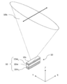
- FIG. 1A is a perspective view schematically showing an example of a light deflector.
- FIG. 1B is a view of the configuration shown in FIG. 1A viewed along the + Y direction.
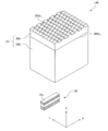
- FIG. 2 is a perspective view schematically showing an example of an optical device according to the first embodiment of the present disclosure.
- FIG. 3A is a view of the configuration shown in FIG. 2 along the + Y direction.
- FIG. 3B is a view of the configuration shown in FIG. 2 along the + Y direction.
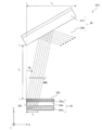
- FIG. 4 is a view of the configuration shown in FIG. 2 along the + X direction.
- FIG. 5A is a diagram plotting the calculation result of the relationship between the width of the light deflector and the spread angle of the light beam when there is no optical element.
- FIG. 5A is a diagram plotting the calculation result of the relationship between the width of the light deflector and the spread angle of the light beam when there is no optical element.
- FIG. 5B is a diagram plotting the calculation result of the relationship between the width of the light deflector and the spread angle of the light beam when there is an optical element.
- FIG. 6A is a perspective view schematically showing an example of an optical device in the first modification of the first embodiment.
- FIG. 6B is a view of the configuration shown in FIG. 6A viewed along the + X direction.
- FIG. 7A is a perspective view schematically showing an example of an optical device in the second modification of the first embodiment.
- FIG. 7B is a view of the configuration shown in FIG. 7A viewed along the + X direction.
- FIG. 8A is a perspective view schematically showing an example of an optical device according to a third modification of the first embodiment.
- FIG. 8B is a view of the configuration shown in FIG.
- FIG. 8A viewed along the + X direction.
- FIG. 8C is a diagram schematically showing the intensity distribution of the light beam emitted from the lens array and the single lens in the far field.
- FIG. 9 is a perspective view schematically showing an example of an optical device according to a fourth modification of the first embodiment.
- FIG. 10A is a perspective view schematically showing an example of an optical device according to a fifth modification of the first embodiment.
- FIG. 10B is a view of the configuration shown in FIG. 10A viewed along the + Y direction.
- FIG. 10C is a perspective view schematically showing an example of an optical device according to a sixth modification of the first embodiment.
- FIG. 10D is a view of the configuration shown in FIG. 10C as viewed along the + Y direction.
- FIG. 10E is a perspective view schematically showing an example of an optical device in the seventh modification of the first embodiment.
- FIG. 10F is a view of the configuration shown in FIG. 10E as viewed along the + Y direction.
- FIG. 11 is a perspective view schematically showing an example of the optical device according to the second embodiment of the present disclosure.
- FIG. 12A is a view of the configuration shown in FIG. 11 along the + Y direction.
- FIG. 12B is a view of the configuration shown in FIG. 11 as viewed along the + Y direction.
- FIG. 13 is a view of the configuration shown in FIG. 11 along the + X direction.
- FIG. 14 is a perspective view schematically showing an example of the optical device 300 according to the third embodiment of the present disclosure.
- FIG. 12A is a view of the configuration shown in FIG. 11 along the + Y direction.
- FIG. 12B is a view of the configuration shown in FIG. 11 as viewed along the + Y direction.
- FIG. 13 is a view
- FIG. 15A is a view of the configuration shown in FIG. 14 viewed along the + Y direction.
- FIG. 15B is a view of the configuration shown in FIG. 14 along the + X direction.
- FIG. 16A is a perspective view schematically showing an example of the optical device 310 in the modified example of the third embodiment.
- FIG. 16B is a view of the configuration shown in FIG. 16A viewed along the + Y direction.
- FIG. 1A is a perspective view schematically showing an example of the structure included in the light deflection device 10 according to the exemplary embodiment.
- FIG. 1B is a view of the configuration shown in FIG. 1A viewed along the + Y direction.
- the X-axis, Y-axis, and Z-axis that are orthogonal to each other are schematically shown.
- the direction in which the arrow of the axis points is the + direction, and the opposite direction is the-direction.
- the direction pointed to by the + Z direction is upward, and the direction pointed to by the -Z direction is downward.
- these names are used only for convenience of explanation, and do not limit the posture when the light deflector 10 is actually used.
- the shape and size of all or part of the structure shown in the drawings does not limit the actual shape and size.
- the light deflector 10 emits a light beam emitted from a light source (not shown) in a predetermined direction.
- the optical deflector 10 includes a first mirror 10m 1, a second mirror 10m 2 , and an optical waveguide layer 10w.
- the first mirror 10m 1 and the second mirror 10m 2 face each other and extend in the X direction.
- the transmittance of the first mirror 10m 1 is higher than that of the second mirror 10m 2.
- At least one of the first mirror 10m 1 and the second mirror 10m 2 can be formed, for example, from a multilayer reflective film in which a plurality of high refractive index layers and a plurality of low refractive index layers are alternately laminated.
- the first mirror 10m 1 and the second mirror 10m 2 can be formed from a multilayer reflective film containing the same high refractive index layer and the same low refractive index layer. In this case, if the number of stacked first mirror 10 m 1 less than the second number of stacked layers of the mirror 10 m 2, the transmittance of the first mirror 10 m 1 is higher than the second transmittance of the mirror 10 m 2.
- the optical waveguide layer 10w is located between the first mirror 10m 1 and the second mirror 10m 2.
- the first mirror 10m 1 has a light emitting surface 10s parallel to the XY plane on the side opposite to the optical waveguide layer 10w.
- the light 10L propagates in the optical waveguide layer 10w along the X direction while being reflected by the first mirror 10m 1 and the second mirror 10m 2. At that time, a part of the light 10L is emitted to the outside as a light beam 10b from the light emitting surface 10s.
- the direction of the central axis of the optical beam 10b depends on the refractive index and / or thickness of the optical waveguide layer 10w. In the present specification, the direction of the central axis of the light beam 10b is simply referred to as "the emission direction of the light beam 10b".
- the optical waveguide layer 10w may have a configuration in which the refractive index and / or the thickness changes according to the change in the applied drive voltage.
- the optical waveguide layer 10w contains a liquid crystal material, and the optical waveguide layer 10w may be provided with two electrodes 10e for applying a driving voltage.
- the drive voltage changes due to the input of a control signal from a control circuit (not shown)
- the refractive index of the optical waveguide layer 10w changes, and the emission direction of the light beam 10b emitted from the light emission surface 10s changes along the X direction. To do.
- the optical waveguide layer 10w contains a gas or liquid
- the first mirror 10m 1 and / or the second mirror 10m 2 may be fitted with an actuator that deforms when a drive voltage is applied.
- the thickness of the optical waveguide layer 10w changes according to the change in the mirror spacing due to the deformation of the actuator, and the light beam emitted from the light emitting surface 10s.
- the emission direction of 10b changes along the X direction.
- the light deflection device 10 can change the emission direction of the light beam 10b emitted from the light emission surface 10s along the X direction in response to the control signal from the outside.
- the thick line parallel to the X direction in FIG. 1A represents the scanning direction of the light beam 10b.
- the shape of the light beam 10b means the shape of a light spot obtained by irradiating the screen with the light beam 10b when there is a screen perpendicular to the emission direction of the light beam 10b in the far field.
- the light beam 10b emitted from the light emitting surface 10s extending along the X direction has a shape extending along the Y direction such as a line shape or an elliptical shape in the far field.
- the divergence angle of the light beam 10b in the Y direction is larger than the divergence angle of the light beam 10b in the X direction.
- the degree of spread of the light beam 10b in the Y direction is appropriately determined according to the application of the LiDAR system. It will be adjusted.
- the distance to an object at a short distance is measured with a small number of scans by changing the light beam extending along the horizontal direction of the road along the vertical direction of the road. can do.
- the distance to the object at a long distance can be measured by increasing the irradiation energy per unit area of the light beam 10b by relatively reducing the extent of the spread of the light beam 10b in the horizontal direction of the road. ..
- the degree of spread of the light beam 10b emitted from the light deflector 10 in the Y direction is determined by the structure of the light deflector 10, specifically, the width of the light emitting surface 10s in the Y direction.
- the spread of the light beam 10b cannot be significantly changed only by the design of the structure.
- the degree of spread of the light beam 10b in the Y direction can be significantly changed by arranging the optical element on the path of the light beam 10b emitted from the light deflection device 10. ..
- the optical device is in the second direction from the light emitting surface parallel to the first direction and the second direction intersecting the first direction toward the direction intersecting the light emitting surface.
- a light deflector that emits a light beam having an elongated shape, which is capable of changing the emission direction of the light beam along the first direction, and is arranged on the path of the light beam.
- An optical element that expands the degree of spread of the light beam in the second direction.
- the optical device according to the second item includes at least one lens in which the optical element has a curvature in the second direction in the optical device according to the first item.
- the optical device according to the third item is the optical device according to the second item, in which the lens is a concave lens.
- the concave lens can magnify the extent of the spread of the light beam emitted from the optical element.
- the optical device according to the fourth item is the optical device according to the second item, in which the lens is a convex lens.
- the convex lens can increase or decrease the extent of the spread of the light beam emitted from the optical element.
- the optical device according to the fifth item is the optical device according to any one of the second to fourth items, wherein the optical element has a portion in which the curvature of the lens changes along the first direction.
- the optical device according to the sixth item is the optical device according to any one of the first to fifth items, in which the optical element is in contact with the light emitting surface of the light deflector.
- the overall size can be reduced by bringing the optical element into contact with the light emitting surface of the light deflector.
- the optical device includes at least one mirror in which the optical element has a curvature in the second direction in the optical device according to any one of the first items.
- the mirror reflects the light beam emitted from the light emitting surface of the light deflector.
- the optical device according to the eighth item is the optical device according to the seventh item, and the mirror is a convex mirror.
- the degree of spread of the light beam emitted from the optical element can be expanded by the convex mirror.
- the optical device according to the ninth item is the optical device according to the seventh item, and the mirror is a concave mirror.
- the concave mirror can increase or decrease the extent of the spread of the light beam emitted from the optical element.
- the optical device according to the tenth item is the optical device according to any one of the seventh to ninth items, wherein the optical element has a portion where the curvature of the mirror changes along the first direction.
- the optical device according to the eleventh item is the optical device according to any one of the first to tenth items, wherein the optical deflectors face each other and extend in the first direction with the first mirror and the second mirror.
- An optical waveguide layer located between the first mirror and the second mirror and directing light in the first direction is provided.
- the optical device according to the twelfth item is the optical device according to any one of the first to tenth items, in which the optical deflection devices are arranged along the first direction and extend along the second direction.
- a plurality of optical waveguides and a plurality of phase shifters connected to the plurality of optical waveguides are provided.
- this optical device a part of the light that has passed through the plurality of phase shifters and is incident on the plurality of optical waveguides is emitted to the outside.
- the optical device according to the thirteenth item is the optical device according to the twelfth item, and each of the plurality of waveguides is provided with a grating. The light beam is emitted through the grating.
- an optical beam formed by overlapping a plurality of diffracted lights is emitted via a grating.
- the optical device is in the second direction from the light emitting surface parallel to the first direction and the second direction intersecting the first direction toward the direction intersecting the light emitting surface.
- a light deflector that emits a light beam having an elongated shape, which is capable of changing the emission direction of the light beam along the first direction, and is arranged on the path of the light beam.
- the optical element includes an optical element that changes the degree of spread of the light beam in the second direction, and the optical element has a first surface on which the light beam is incident and a second surface on which the light beam is emitted. The distance between the light emitting surface and the first surface or the second surface of the optical element along the direction perpendicular to the light emitting surface changes along the first direction.
- the optical device according to the fifteenth item is the optical device according to the fourteenth item, wherein the optical element includes at least one lens having a curvature in the second direction, and the curvature of the lens is the first direction. It has a part that changes along with.
- the optical device according to the sixteenth item is the optical device according to the fourteenth item, wherein the optical element includes at least one lens having a curvature in the second direction, and the curvature of the lens is the first. It has a portion that is constant along the direction, and the first surface or the second surface of the portion of the optical element is inclined along the first direction with respect to the light emitting surface.
- this optical device it is possible to suppress a change in the optical path length depending on the emission angle while keeping the curvature of the lens constant along the first direction. As a result, changes in the shape and intensity distribution of the light beam due to the beam scan can be suppressed.
- all or part of a circuit, unit, device, member or part, or all or part of a functional block in a block diagram is, for example, a semiconductor device, a semiconductor integrated circuit (IC), or an LSI (range scale integration). ) Can be performed by one or more electronic circuits.
- the LSI or IC may be integrated on one chip, or may be configured by combining a plurality of chips.
- functional blocks other than the storage element may be integrated on one chip.
- it is called LSI or IC, but the name changes depending on the degree of integration, and it may be called system LSI, VLSI (very large scale integration), or ULSI (ultra large scale integration).
- Field Programmable Gate Array (FPGA) which is programmed after the LSI is manufactured, or reconfigurable logistic device, which can reconfigure the junction relationship inside the LSI or set up the circuit partition inside the LSI, can also be used for the same purpose.
- FPGA Field Programmable Gate Array
- circuits, units, devices, members or parts can be executed by software processing.
- the software is recorded on a non-temporary recording medium such as one or more ROMs, optical disks, hard disk drives, etc., and when the software is executed by a processor, the functions identified by the software It is performed by a processor and peripherals.
- the system or device may include one or more non-temporary recording media on which the software is recorded, a processor, and the required hardware devices, such as an interface.
- light refers to electromagnetic waves including not only visible light (wavelength of about 400 nm to about 700 nm) but also ultraviolet rays (wavelength of about 10 nm to about 400 nm) and infrared rays (wavelength of about 700 nm to about 1 mm). means.
- FIG. 2 is a perspective view schematically showing an example of the optical device 100 according to the first embodiment of the present disclosure.
- the optical device 100 according to the first embodiment includes an optical deflection device 10 and an optical element 20.
- the light deflection device 10 in the first embodiment is as described with reference to FIGS. 1A and 1B.
- the light source described above may include, for example, a semiconductor laser element.
- the wavelength of the light beam emitted from the light source can be selected according to the application. When the distance to the object is measured by infrared rays, the wavelength of the light beam can be, for example, 700 nm or more and 2.5 ⁇ m or less.
- the wavelength of the light beam may be a wavelength in the visible region, that is, about 400 nm or more and about 700 nm or less.
- the wavelength of the light beam may be 2.5 ⁇ m or more.
- the optical element 20 in the first embodiment includes a lens 20a and a medium 20b that supports the lens 20a.
- the optical element 20 is arranged on the path of the light beam 10b emitted from the light deflector 10.
- the lens 20a is a plano-concave lens having an upper surface 20as 1 and a lower surface 20as 2. In FIG. 2, the curvature of the lens 20a is exaggerated.
- the lens 20a has a curvature in the Y direction on the upper surface 20as 1 and a flat bottom surface on the lower surface 20as 2. The curvature is defined by the reciprocal of the radius of curvature.
- the lens 20a is a cylindrical lens having a structure extending in the X direction.
- the lens 20a may have a curvature in at least one of the upper surface 20as 1 and the lower surface 20as 2 in the Y direction.
- the radius of curvature can be, for example, 1 mm or more and 100 mm or less.
- the medium 20b has the same refractive index as the lens 20a, but may have a different refractive index.
- the medium 20b is in contact with the light emitting surface 10s of the light deflecting device 10.
- the medium 20b may not be in contact with the light emitting surface 10s of the light deflecting device 10 depending on the application.
- the medium 20b may be air, water, or vacuum.
- the optical element 20 does not have to include both the lens 20a and the medium 20b, and may include at least one of them.
- the length of the optical element 20 in the X direction may be, for example, 1 mm or more and 5 mm or less
- the width in the Y direction may be, for example, 1 mm or more and 10 mm or less
- the height in the Z direction may be, for example, 1 mm or more and 10 mm or less.
- FIGS. 3A and 3B are views of the configuration shown in FIG. 2 along the + Y direction.
- the light deflector 10 and the optical element 20 are arranged so that the surfaces viewed along the + X direction are aligned.
- the emission direction of the optical beam 10b changes along the X direction.
- the emission angle of the light beam 10b is changed from phi 1 to phi 2.
- the emission angle of the light beam 10b corresponds to the angle formed by the plane parallel to the YZ plane and the light beam 10b.
- phi 1 and phi 2 have both positive values.
- the intensity of the light 10L decreases along the X direction.
- the distance at which the intensity of light 10L becomes 1 / e times the propagation length l x. e is the base of the natural logarithm.
- the length L x of the optical element 20 in the X direction is the propagation length l. Designed longer than x. Specifically, the length L x of the optical element 20 is designed according to the propagation length l x , the maximum emission angle ⁇ 2 of the light beam 10 b, and the height L z of the optical element 20 in the Z direction.
- the light beam 10b is refracted by the upper surface 20as 1 of the lens 20a and emitted to the outside.
- FIG. 4 is a view of the configuration shown in FIG. 2 along the + X direction.
- the light rays with arrows represent how the light beam 10b emitted from the light deflector 10 propagates.
- the optical element 20 emits light incident on the optical element 20 in a direction different from the incident direction due to the refraction effect.
- a diffraction effect may be used instead of the refraction effect, or both a refraction effect and a diffraction effect may be used.
- the light beam 10b is microscopically emitted from the light emitting surface 10s having a width in the Y direction, but is described so as to be emitted from one point for the sake of simplicity.
- the structure of the optical element 20 is as follows. Let n be the refractive index of the lens 20a and the medium 20b. The spread angle of the light beam 10b emitted from the light emitting surface 10s and propagating in the medium 20b is represented by a half-width character and is set to ⁇ 1. The spread angle of the light beam 10b emitted from the lens 20a to the outside is represented by a half-width character and is defined as ⁇ 2 .
- w be the width of the light deflector 10. The width of the light deflector 10 is equal to the width of the light emitting surface 10s.
- r 0 be the half width of the lens 20a in the y direction
- f be the focal length of the lens 20a when viewed along the emission direction of the beam 10b.
- s 1 be the distance between the principal point H of the lens 20a and the focusing point F of the light propagating in the medium 20b.
- ⁇ s 2 be the distance between the principal point H of the lens 20a and the focusing point F of the light emitted to the outside.
- the principal point H is the principal point when the emission direction of the light beam 10b in the optical element 20 is the optical axis, and s 1 and ⁇ s 2 are in the emission direction of the light beam 10b in the optical element 20. The distance along.
- the spread angle ⁇ 1 of the light beam 10b emitted from the light emitting surface 10s will be described. It is assumed that the intensity distribution of the light beam 10b emitted from the light emitting surface 10s in the Y direction shows a shape close to a rectangular shape in the near field, and the width thereof is the width w of the light deflector 10. Assuming that the wavelength of the light beam 10b is ⁇ , the light intensity I at a location separated by y from the center of the light deflector 10 along the Y direction and z away from the light emitting surface 10s along the Z direction is as follows. It is represented by the equation (1).
- the distribution of light intensity I in the Y direction has a central peak called the main lobe and a plurality of small peaks on both sides thereof.
- the width of the light beam 10b is the width of the main lobe
- the half width of the main lobe is expressed by the following equation (2).
- the spread angle ⁇ 1 of the light beam 10b is expressed by the following equation (3).
- the spread angle ⁇ 1 is approximately expressed by the following equation (5).
- the spread angle ⁇ 2 of the light beam 10b emitted from the optical element 20 to the outside will be described.
- the curvature of the lens 20a is gentle, the distance between the upper surface 20AS 1 and the lower surface 20AS 2 in the lens 20a is relatively short compared to the distance s 1.
- the distance s 1 is approximately expressed by the following equation (6).
- the distance s 1 and the distance s 2 satisfy the following equation (7).
- the distance s 2 is expressed by the following equation (8).
- the focal length f is represented by a negative value. Therefore, the smaller the absolute value of the focal length f and the larger r, the larger the spread angle ⁇ 2 .
- the focal length f is expressed by the following equation (10).
- FIG. 5A is a diagram plotting the calculation result of the relationship between the width w of the light deflector 10 and the spread angle ⁇ 1 of the light beam 10b when the optical element 20 is not present.
- FIG. 5B is a diagram plotting the calculation result of the relationship between the width w of the light deflector 10 and the spread angle ⁇ 2 of the light beam 10b when the optical element 20 is present.
- the width w of the light deflector 10 is 1 ⁇ m or more and 10 ⁇ m.
- the reason for designing the width w of the light deflector 10 within this range is as follows. If the light deflector 10 is manufactured with high processing accuracy in order to make the width w of the light deflector 10 narrower than 1 ⁇ m, the manufacturing cost becomes high. Further, the narrower the width w of the optical deflector 10, the greater the exudation of the light 10L propagating in the optical waveguide layer 10w to the outside in the Y direction. Due to the large exudation to the outside, the propagation efficiency of the light 10L in the optical waveguide layer 10w is lowered, and the efficiency of the light beam 10b emitted from the light emitting surface 10s is lowered.
- the width of the light emitting surface 10s in the Y direction becomes substantially wide, and the spread angle ⁇ 1 of the light beam 10b cannot be increased as expected. ..
- the width w of the light deflector 10 is made wider than 10 ⁇ m, the size of the chip including the light deflector 10 is increased, and the manufacturing cost is increased.
- the relationship between the width w of the optical deflector 10 and the spread angle ⁇ 1 of the optical beam 10b takes into consideration the exudation of light from the optical waveguide layer 10 to the outside in addition to the equation (4).
- the width w of the light deflector 10 is designed in the range of 1 ⁇ m or more and 10 ⁇ m or less
- the spread angle ⁇ 1 of the light beam 10b is 6 ° or more and 34 ° or less.
- the relationship between the width w of the optical deflector 10 and the spread angle ⁇ 2 of the optical beam 10b is determined by the optical waveguide layer 10 in addition to the equations (4), (6) and (11). It was calculated in consideration of the exudation of light from.
- the broken line portion shown in FIG. 5B represents an unrealizable spread angle ⁇ 2 because the radius r of the light beam 10b exceeds the radius of curvature R of the lens 20a.
- the spread angle ⁇ 2 of the light beam 10b is 8 ° or more and 42 ° or less.
- the spread angle ⁇ 1 of the light beam 10b is 6 ° or more and 34 ° or less within the range of the same width w.
- the spread angle ⁇ 2 of the light beam 10b is 10 ° or more and 36 ° or less. become.
- the spread angle ⁇ 1 of the light beam 10b is 6 ° or more and 23 ° or less within the range of the same width w.
- the spread angle ⁇ 2 of the light beam 10b is 12 ° or more and 33 ° or less. become.
- the spread angle ⁇ 1 of the light beam 10b is 6 ° or more and 17 ° or less within the range of the same width w.
- the spread angle ⁇ 2 of the light beam 10b in the presence of the optical element 20 is compared with the spread angle ⁇ 1 of the light beam 10 b in the absence of the optical element 20. Will be expanded.
- the spread angle ⁇ 2 of the light beam 10b can be increased without narrowing the width w of the light deflection device 10 with high processing accuracy.
- the light beam 10b allows a wider area to be scanned with a smaller number of times.
- the optical element 20 in the optical device 100 may include a lens other than the plano-concave lens 20a extending in the X direction shown in FIG.
- FIG. 6A is a perspective view schematically showing an example of the optical device 110 in the first modification of the first embodiment.
- FIG. 6B is a view of the configuration shown in FIG. 6A viewed along the + X direction.
- the difference between the optical device 110 in the first modification and the optical device 100 in the first embodiment is that the lens 20a included in the optical element 20 is a plano-convex lens.
- the curvature of the plano-convex lens 20a in the Y direction is relatively small.
- the spread angle ⁇ 2 of the light beam 10b becomes smaller. Since the irradiation energy per unit area of the light beam 10b is high, the light beam 10b can scan an object at a long distance.
- FIG. 7A is a perspective view schematically showing an example of the optical device 120 in the second modification of the first embodiment.
- FIG. 7B is a view of the configuration shown in FIG. 7A viewed along the + X direction.
- the difference between the optical device 120 in the second modification and the optical device 110 in the first modification is that the curvature of the convex lens 20a in the Y direction is relatively large.
- the light beam 10b is emitted from the convex lens 20a, then focused once, and then diffused. In this case, the spread angle ⁇ 2 of the light beam 10b becomes large.
- the spread angle ⁇ 2 of the light beam 10b can be enlarged or reduced according to the curvature of the convex lens 20a.
- FIG. 8A is a perspective view schematically showing an example of the optical device 130 in the third modification of the first embodiment.
- FIG. 8B is a view of the configuration shown in FIG. 8A viewed along the + X direction.
- the difference between the optical device 130 in the third modification and the optical device 100 in the first embodiment is that the lenses 20a included in the optical element 20 are arranged in a lens array including a plurality of concave lenses regularly arranged in the Y direction. That is.
- the plurality of concave lenses may be randomly arranged along the Y direction, or the curvatures of the individual concave lenses may vary.
- the lens array 20a covers the spot range of the light beam 10b incident on the lens array 20a.
- the beam radius r on the lens 20a cannot exceed the radius of curvature R of the lens.
- the third modification there is no such limitation. This is because even if the radius of curvature R of each concave lens is smaller than the beam radius r of the light beam 10b, the plurality of concave lenses cover the spot range of the light beam 10b. As described above, the spread angle ⁇ 2 of the light beam 10b at the broken line portion shown in FIG. 5B can be realized, so that the spread angle ⁇ 2 can be further increased.
- FIG. 8C is a diagram schematically showing the intensity distribution in the far field of the light beam 10b emitted from the lens array and the single lens.
- the solid line and the broken line represent the intensity distribution of the light beam 10b emitted from the lens array and the single lens, respectively.
- the intensity of the light beam 10b is near zero at both ends of the main lobe.
- the intensity at both ends of the light beam 10b is higher, and the maximum intensity at the center of the light beam 10b is lower.
- the individual concave lenses diffuse the incident light, so that the non-uniformity of the intensity distribution can be alleviated as shown in FIG. 8C. Therefore, a wider area in the Y direction can be irradiated with the low intensity light beam 10b.
- FIG. 9 is a perspective view schematically showing an example of the optical device 140 in the fourth modification of the first embodiment.
- the lenses 20a included in the optical element 20 include a plurality of concave lenses that are regularly arranged along the X and Y directions. It is a lens array.
- the plurality of concave lenses may be randomly arranged along the X and Y directions, or the curvatures of the individual concave lenses may vary.
- the light beam 10b emitted from the light emitting surface 10s is diffused in both the X direction and the Y direction. For the reasons described with reference to FIG. 8C, a wider area in the X and Y directions can be irradiated with the low intensity light beam 10b.
- the intensity of laser light is classified by class according to JIS (Japanese Industrial Standards) C6802 "Safety Standards for Laser Products".
- the intensity of the laser beam is preferably class 1 from the viewpoint of eye safety. Even if the intensity distribution of the light beam 10b emitted from the light emitting surface 10s does not satisfy class 1, it is emitted from the optical element 20 by diffusing the light beam 10b by the optical elements 20 shown in FIGS. 8A and 9.
- the intensity distribution of the light beam 10b can be made to satisfy class 1.
- FIG. 10A is a perspective view schematically showing an example of the optical device 150 in the fifth modification of the first embodiment.
- FIG. 10B is a view of the configuration shown in FIG. 10A viewed along the + Y direction.
- the broken line shown in FIGS. 10A and 10B is a line connecting the stop points of the concave lens 20a in the Y direction.
- the difference between the optical device 130 in the fifth modification and the optical device 100 in the first embodiment is that the curvature of the lens 20a included in the optical element 20 in the Y direction changes monotonically along the X direction. ..
- the optical element 20 has a portion in which the curvature of the lens 20a in the Y direction changes along the X direction. As shown in FIG.
- the curvature of the lens 20a with respect to the light beam 10b at a certain emission angle can be known from the cut surface of the lens 20a when the lens 20a is cut by the following plane.
- the plane is a plane parallel to both the emission direction of the light beam 10b and the Y direction in the optical element 20.
- the curvature of the lens 20a in the Y direction is constant along the X direction, the curvature of the lens 20a with respect to the light beam 10b increases with the emission angle of the light beam 10b.
- the curvature of the lens 20a in the Y direction is monotonically reduced along the + X direction to make the curvature of the lens 20a with respect to the light beam 10b constant regardless of the emission angle. be able to.
- the spread angle ⁇ 2 of the light beam 10b is constant regardless of the emission angle of the light beam 10b.
- the shape and intensity distribution of the light beam 10b do not depend on the emission angle of the light beam 10b. Even if the curvature of the lens 20a with respect to the light beam 10b is not strictly constant regardless of the emission angle, it is possible to suppress a change in the shape and intensity distribution of the light beam 10b due to a change in the emission angle.
- the upper surface 20as 1 of the optical element 20 is used as the lens surface, and the curvature of the upper surface 20as 1 is changed along the X direction, but the lower surface 20as 2 of the optical element 20 is used as the lens surface.
- the curvature of the lower surface 20as 2 may be changed along the X direction.
- the upper surface 20as 1 may be flat.
- FIG. 10C is a perspective view schematically showing an example of the optical device 160 in the sixth modification of the first embodiment.
- FIG. 10D is a view of the configuration shown in FIG. 10C as viewed along the + Y direction. Similar to the above embodiment, the medium 20b does not have to be in contact with the light emitting surface 10s of the light deflecting device 10.
- the optical element 20 of the optical device 160 in the sixth modification has a portion in which the curvature of the lens 20a in the Y direction is constant along the X direction.
- the difference between the optical device 160 in the sixth modification and the optical device 100 in the first embodiment is that the light emitting side surface of the optical element 20 in the lens 20a and the upper surface 20as 1 which is the lens surface are lighted by the deflector 10.
- the focal length of the lens 20a is constant along the X direction.
- the light 10b from the light deflection element 10 can be regarded as emitted from one sufficiently small point.
- the shape and intensity distribution of the light beam 10b changes depending on the emission angle. This is because the optical path length from the emission point of the light beam 10b to the lens surface 20as 1 fluctuates even though the focal length of the lens 20a is constant.
- the fluctuation of the optical path length can be suppressed.
- the angle ⁇ is equal to the middle of the emission angle range of the light beam 10b (that is, ( ⁇ 1 + ⁇ 2 ) / 2).
- the optical path length from the emission point of the light deflection element 10 to the lens surface at an intermediate emission angle of 20 ° is set to 10 mm.
- ⁇ 0 °
- the optical device 160 in the sixth modification it is possible to suppress the change in the optical path length depending on the emission angle while keeping the curvature of the lens 20a constant along the X direction. As a result, changes in the shape and intensity distribution of the light beam 10b due to the beam scan can be suppressed.
- the lower surface 20as 2 of the optical element 20 is tilted along the X direction, but it may be parallel to the light emitting surface 10s of the light deflector 10. Further, although the light incident surface of the medium 20 is parallel to the light emitting surface 10s, it may be tilted along the X direction.
- the lens surface of the lens 20a may be formed on the lower surface 20as 2 which is the surface on the incident side.
- 10E and 10F are perspective views schematically showing an example of the optical device 170 in the seventh modification of the first embodiment.
- the difference between the optical device 170 in the seventh modification and the optical device 160 in the sixth modification is the distance between the light emitting surface 10s and the lower surface 20as 2 of the optical element 20 along the direction perpendicular to the light emitting surface 10s. , It is changing along the X direction.
- the upper surface 20as 1 of the optical element 20 is parallel to the light emitting surface 10s of the light deflector 10, but it may be tilted along the X direction. Further, although the light incident surface of the medium 20 is parallel to the light emitting surface 10s, it may be tilted along the X direction.
- FIG. 11 is a perspective view schematically showing an example of the optical device 200 according to the second embodiment of the present disclosure.
- the optical device 200 according to the second embodiment includes an optical deflection device 30 and an optical element 20.
- the optical deflection device 30 includes a plurality of optical waveguides 30w and a plurality of phase shifters 30p connected to the plurality of optical waveguides 30w, respectively.
- the plurality of optical waveguides 30w are arranged along the X direction and extend along the Y direction.
- the number of the plurality of optical waveguides 30w can be, for example, 8 or more and 64 or less.
- Each of the plurality of optical waveguides 30w is provided with a light emitting region 30r on the surface for emitting light.
- a grating of 30 g is provided in each of the plurality of light emitting regions 30r.
- the optical waveguide 30w has a higher refractive index than an external medium such as air.
- the optical waveguide 30w propagates light along the Y direction by total reflection.
- the light propagating along the optical waveguide 30w in the Y direction is emitted to the outside from the light emitting region 30r as a plurality of diffracted lights parallel to the YZ plane due to the diffraction by the grating 30g.
- the length of the light emitting region 30r in the Y direction can be, for example, 1 ⁇ m or more and 10 ⁇ m or less.
- the number of recesses in the grating of 30 g can be set to, for example, 4 or more and 16 or less.
- the length of the recesses in the Y direction per cycle in the grating of 30 g, that is, the duty ratio may be appropriately changed depending on the depth and the number of the recesses of the grating.
- an optical beam is formed by the interference of light emitted from a plurality of optical waveguides 30w. It can also be said that the light beam is emitted to the outside from the light emitting surface 30s including the plurality of light emitting regions 30r.
- the light beam has a shape extending in the Y direction due to the overlap of a plurality of diffracted lights parallel to the YZ plane.
- the plurality of phase shifters 30p are arranged along the X direction and extend along the Y direction, similarly to the plurality of optical waveguides 30w.
- the phase shifter 30p may have a configuration in which the refractive index changes according to a change in the applied drive voltage.
- the phase shifter 30p can be formed from a thermo-optical material whose refractive index changes with temperature.
- the phase shifter 30p includes a heater (not shown) that changes the temperature of the thermo-optical material.
- the heater (not shown) is provided with two electrodes for applying a driving voltage.
- the phase shifter 30p can be formed from an electro-optical material whose refractive index changes with a change in driving voltage.
- the phase shifter 30p is provided with two electrodes for applying a driving voltage to the electro-optical material.
- the drive voltage changes due to the input of a control signal from a control circuit (not shown)
- the refractive index of the phase shifter 30p changes and the phase of light passing through the phase shifter 30p changes.
- the drive voltage changes in response to the control signal, and the phases of the light incident on the plurality of optical waveguides 30w from the plurality of phase shifters 30p are arranged in a plurality of optical waveguides 30w. It changes by a certain amount in order. By this phase shift, the emission direction of the light beam can be changed along the X direction.
- FIGS. 12A and 12B are views of the configuration shown in FIG. 11 as viewed along the + Y direction.
- the light deflector 30 and the optical element 20 are arranged so as to be in contact with each other and symmetrical with respect to a plane parallel to the YZ plane.
- the emission angle of the light beam 30b is changed from phi 1 to phi 2.
- ⁇ 1 has a negative value and ⁇ 2 has a positive value.
- the absolute value of ⁇ 1 and the absolute value of ⁇ 2 may be equal or different.
- the length L x of the optical element 20 in the X direction is an optical deflector. It is designed to be longer than the length d x in the X direction of 30.
- the optical element 20 length L x has a length d x of the optical deflection device 30, the minimum emission angle phi 1 of the light beam 30b, the maximum emission angle phi 2 of the light beams 30b, and the optical element 20 It is designed according to the height L z in the Z-direction.
- the light beam 30b is refracted by the upper surface 20as 1 of the lens 20a and emitted to the outside.
- FIG. 13 is a view of the configuration shown in FIG. 11 along the + X direction.
- the optical element 20 in the second embodiment is as described with reference to FIG.
- the spread angle ⁇ 2 of the light beam 30b is increased by the optical element 20.
- the optical element 20 in the second embodiment the optical element 20 in the first to fifth modified examples of the first embodiment may be used.
- the spread angle ⁇ 2 of the light beam 30b can be changed by providing the optical element 20 on the light deflection device 30. Therefore, it is possible to easily obtain a light beam 30b having a degree of spread according to the application.
- FIG. 14 is a perspective view schematically showing an example of the optical device 300 according to the third embodiment of the present disclosure.
- the difference between the optical device 300 in the third embodiment and the optical device 100 in the first embodiment is that the optical element 20 includes a mirror 20c instead of the lens 20a.
- the optical element 20 in the third embodiment includes a mirror 20c and a medium 20b.
- the mirror 20c is a plano-convex mirror having an upper surface 20cs 1 and a lower surface 20cs 2.
- the mirror 20c has a flat surface on the upper surface 20as 1 and a curvature in the Y direction on the lower surface 20cs 2.
- the lower surface 20cs 2 of the mirror 20c corresponds to a reflecting surface.
- the reflectance of the reflecting surface can be, for example, 90% or more at the wavelength of the light beam 10b.
- the mirror 20c is a cylindrical mirror having a structure extending in the X direction.
- the curvature of the plano-convex mirror is equal to the curvature of the plano-concave lens in Embodiment 1.
- the medium 20b is as described above. In the example shown in FIG. 14, the medium 20b is air. In the example shown in FIG.
- the direction in which the reflecting surface 20cs 2 in the mirror 20c extends is parallel to the direction in which the light emitting surface 10s in the light deflector 10 extends. As described above, the reflecting surface 20cs 2 in the mirror 20c faces the light emitting surface 10s in the light deflecting device 10.
- 15A and 15B are views of the configuration shown in FIG. 14 as viewed along the + Y and + X directions, respectively.
- the light beam 10b emitted upward from the light deflector 10 is reflected downward by the mirror 20c.
- the shortest distance L z of the light emitting surface 10s at the reflecting surface 20cs2 and the light deflector 10 in the mirror 20c is more preferably designed to satisfy the following conditions.
- the conditions are emitted at a minimum emission angle phi 1
- the light beam 10b which is reflected by the reflecting surface 20 cs 2 the mirror 20c is that it does not re-enter the light emission surface 10s. This re-incident leads to a loss of the light beam 10b emitted to the outside.
- the degree of spread of the light beam 10b reflected downward becomes large.
- the focusing point F of the light reflected by the mirror 20c is located above the lower surface 20cs 2 of the mirror 20c.
- the plano-concave lens in the first embodiment is replaced with a plano-convex mirror, the degree of spread of the light beam 10b is similarly magnified, although there is a difference between transmission and reflection of the light beam 10b.
- FIG. 16A is a perspective view schematically showing an example of the optical device 310 in the modified example of the third embodiment.
- FIG. 16B is a view of the configuration shown in FIG. 16A viewed along the + Y direction.
- the difference between the optical device 310 in the modified example of the third embodiment and the optical device 300 in the third embodiment is that the direction in which the reflecting surface 20cs 2 in the mirror 20c extends is parallel to the direction in which the light emitting surface 10s in the light deflecting device 10 extends. It is not.
- the reflecting surface 20cs 2 in the mirror 20c is inclined with respect to the light emitting surface 10s in the light deflecting device 10. Therefore, the possibility that the light beam 10b reflected downward by the reflecting surface 20cs 2 in the mirror 20c re-enters the light emitting surface 10s can be significantly reduced. Furthermore, as shown in FIG. 16B, it is possible to shorten the shortest distance L z of the light emitting surface 10s of the reflective surface 20 cs 2 and the optical deflector 10 in the mirror 20c. If it is possible to shorten the shortest distance L z, as compared with the example shown in FIG. 15B, before the light beam 10b emitted from the light deflecting device 10 is widely spread, it can be to reflect the light beam 10b by the mirror 20c .. Therefore, the size of the mirror 20c in the Y direction can be reduced.
- the light emitting surface 10s of the light deflecting device 10 faces the direction in which the reflecting surface 20cs 2 of the mirror 20c is located, as shown in FIGS. 14 and 16A.
- the light beam 10b emitted from the light emitting surface 10s of the light deflecting device 10 is incident on the reflecting surface 20cs 2 of the mirror 20c.
- the light beam 10b spreads although there is a difference between transmission and reflection of the light beam 10b.
- the degree of is scaled up or down in the same way.
- the mirror 20c may include a plurality of mirrors as shown in FIGS. 8A and 9. As shown in FIG. 10A, the mirror 20c may have a portion where the curvature in the Y direction changes along the X direction.
- the optical device according to the embodiment of the present disclosure can be used, for example, for measuring the distance to an object.
Landscapes
- Physics & Mathematics (AREA)
- General Physics & Mathematics (AREA)
- Optics & Photonics (AREA)
- Engineering & Computer Science (AREA)
- Nonlinear Science (AREA)
- Remote Sensing (AREA)
- Computer Networks & Wireless Communication (AREA)
- Radar, Positioning & Navigation (AREA)
- Electromagnetism (AREA)
- Condensed Matter Physics & Semiconductors (AREA)
- Lenses (AREA)
- Facsimile Scanning Arrangements (AREA)
- Optical Modulation, Optical Deflection, Nonlinear Optics, Optical Demodulation, Optical Logic Elements (AREA)
- Mechanical Optical Scanning Systems (AREA)
Priority Applications (6)
| Application Number | Priority Date | Filing Date | Title |
|---|---|---|---|
| CN202080062627.3A CN114341726B (zh) | 2019-09-27 | 2020-08-05 | 光设备 |
| CN202511326787.5A CN120891686A (zh) | 2019-09-27 | 2020-08-05 | 光设备 |
| JP2021548405A JPWO2021059757A1 (https=) | 2019-09-27 | 2020-08-05 | |
| US17/695,743 US12248140B2 (en) | 2019-09-27 | 2022-03-15 | Optical device |
| JP2025006728A JP2025061430A (ja) | 2019-09-27 | 2025-01-17 | 光デバイス |
| US19/045,238 US20250180893A1 (en) | 2019-09-27 | 2025-02-04 | Optical device |
Applications Claiming Priority (2)
| Application Number | Priority Date | Filing Date | Title |
|---|---|---|---|
| JP2019176746 | 2019-09-27 | ||
| JP2019-176746 | 2019-09-27 |
Related Child Applications (1)
| Application Number | Title | Priority Date | Filing Date |
|---|---|---|---|
| US17/695,743 Continuation US12248140B2 (en) | 2019-09-27 | 2022-03-15 | Optical device |
Publications (1)
| Publication Number | Publication Date |
|---|---|
| WO2021059757A1 true WO2021059757A1 (ja) | 2021-04-01 |
Family
ID=75166592
Family Applications (1)
| Application Number | Title | Priority Date | Filing Date |
|---|---|---|---|
| PCT/JP2020/029912 Ceased WO2021059757A1 (ja) | 2019-09-27 | 2020-08-05 | 光デバイス |
Country Status (4)
| Country | Link |
|---|---|
| US (2) | US12248140B2 (https=) |
| JP (2) | JPWO2021059757A1 (https=) |
| CN (2) | CN120891686A (https=) |
| WO (1) | WO2021059757A1 (https=) |
Cited By (1)
| Publication number | Priority date | Publication date | Assignee | Title |
|---|---|---|---|---|
| WO2023156982A1 (en) * | 2022-02-21 | 2023-08-24 | Innoviz Technologies Ltd. | Device for emitting a light beam and partial beam splitter |
Citations (9)
| Publication number | Priority date | Publication date | Assignee | Title |
|---|---|---|---|---|
| JPH0534733A (ja) * | 1991-07-31 | 1993-02-12 | Pioneer Electron Corp | レーザ光走査装置 |
| JPH09133887A (ja) * | 1995-11-08 | 1997-05-20 | Toppan Printing Co Ltd | 光ビーム偏向光学装置 |
| WO2005083493A1 (ja) * | 2004-02-27 | 2005-09-09 | Matsushita Electric Industrial Co., Ltd. | 照明光源及びそれを用いた2次元画像表示装置 |
| US20160170287A1 (en) * | 2013-07-30 | 2016-06-16 | Nokia Technologies Oy | Optical beams |
| WO2017126386A1 (ja) * | 2016-01-22 | 2017-07-27 | 国立大学法人横浜国立大学 | 光偏向デバイスおよびライダー装置 |
| WO2018003852A1 (ja) * | 2016-06-30 | 2018-01-04 | 国立大学法人横浜国立大学 | 光偏向デバイスおよびライダー装置 |
| JP2019040066A (ja) * | 2017-08-25 | 2019-03-14 | 国立大学法人京都工芸繊維大学 | 光回路集積装置およびビームステアリングシステム |
| JP2019074361A (ja) * | 2017-10-13 | 2019-05-16 | 国立大学法人東京工業大学 | 3次元計測用プロジェクタおよび3次元計測装置 |
| JP2019520595A (ja) * | 2016-04-11 | 2019-07-18 | ディジレンズ・インコーポレイテッド | 構造化光投影のためのホログラフィック導波管装置 |
Family Cites Families (14)
| Publication number | Priority date | Publication date | Assignee | Title |
|---|---|---|---|---|
| ATE150573T1 (de) * | 1991-12-30 | 1997-04-15 | Philips Electronics Nv | Optische einrichtung und mit einer solchen optischen einrichtung versehenes gerät zum abtasten einer informationsebene |
| JP3666503B2 (ja) * | 1994-12-28 | 2005-06-29 | セイコーエプソン株式会社 | 偏光照明装置および投写型表示装置 |
| NZ537849A (en) * | 2005-01-21 | 2007-09-28 | Peter James Hilton | Direct Retinal Display projecting a scanned optical beam via diverging and converging reflectors |
| KR100888477B1 (ko) * | 2007-02-28 | 2009-03-12 | 삼성전자주식회사 | 1차원 광변조기 및 이를 채용한 화상 출력 장치 |
| RU2410809C1 (ru) * | 2009-06-26 | 2011-01-27 | Государственное образовательное учреждение высшего профессионального образования "Московский физико-технический институт (государственный университет)" | Твердотельный лазер, управляемый электрическим полем, и способ переключения частоты твердотельного лазера |
| JP5565910B2 (ja) | 2011-01-21 | 2014-08-06 | 日本電信電話株式会社 | 光偏向器 |
| JP5662266B2 (ja) * | 2011-07-01 | 2015-01-28 | 株式会社デンソー | 光偏向モジュール |
| US9291874B2 (en) * | 2013-02-06 | 2016-03-22 | Panasonic Intellectual Property Management Co., Ltd. | Optical deflection element and optical deflection device |
| JP6550683B2 (ja) * | 2016-06-16 | 2019-07-31 | 日本電信電話株式会社 | 波長掃引光源 |
| CN106054490B (zh) * | 2016-07-29 | 2018-12-21 | 西安空间无线电技术研究所 | 一种基于光学相控阵的大角度波束控制系统 |
| JP2018124271A (ja) | 2017-01-31 | 2018-08-09 | パナソニックIpマネジメント株式会社 | 撮像システム |
| JP7018564B2 (ja) | 2017-02-09 | 2022-02-14 | パナソニックIpマネジメント株式会社 | 光スキャンデバイス、光受信デバイス、および光検出システム |
| CN108415205B (zh) | 2017-02-09 | 2022-11-04 | 松下知识产权经营株式会社 | 光扫描设备、光接收设备以及光检测系统 |
| CN108627974A (zh) * | 2017-03-15 | 2018-10-09 | 松下知识产权经营株式会社 | 光扫描系统 |
-
2020
- 2020-08-05 CN CN202511326787.5A patent/CN120891686A/zh active Pending
- 2020-08-05 JP JP2021548405A patent/JPWO2021059757A1/ja active Pending
- 2020-08-05 WO PCT/JP2020/029912 patent/WO2021059757A1/ja not_active Ceased
- 2020-08-05 CN CN202080062627.3A patent/CN114341726B/zh active Active
-
2022
- 2022-03-15 US US17/695,743 patent/US12248140B2/en active Active
-
2025
- 2025-01-17 JP JP2025006728A patent/JP2025061430A/ja active Pending
- 2025-02-04 US US19/045,238 patent/US20250180893A1/en active Pending
Patent Citations (9)
| Publication number | Priority date | Publication date | Assignee | Title |
|---|---|---|---|---|
| JPH0534733A (ja) * | 1991-07-31 | 1993-02-12 | Pioneer Electron Corp | レーザ光走査装置 |
| JPH09133887A (ja) * | 1995-11-08 | 1997-05-20 | Toppan Printing Co Ltd | 光ビーム偏向光学装置 |
| WO2005083493A1 (ja) * | 2004-02-27 | 2005-09-09 | Matsushita Electric Industrial Co., Ltd. | 照明光源及びそれを用いた2次元画像表示装置 |
| US20160170287A1 (en) * | 2013-07-30 | 2016-06-16 | Nokia Technologies Oy | Optical beams |
| WO2017126386A1 (ja) * | 2016-01-22 | 2017-07-27 | 国立大学法人横浜国立大学 | 光偏向デバイスおよびライダー装置 |
| JP2019520595A (ja) * | 2016-04-11 | 2019-07-18 | ディジレンズ・インコーポレイテッド | 構造化光投影のためのホログラフィック導波管装置 |
| WO2018003852A1 (ja) * | 2016-06-30 | 2018-01-04 | 国立大学法人横浜国立大学 | 光偏向デバイスおよびライダー装置 |
| JP2019040066A (ja) * | 2017-08-25 | 2019-03-14 | 国立大学法人京都工芸繊維大学 | 光回路集積装置およびビームステアリングシステム |
| JP2019074361A (ja) * | 2017-10-13 | 2019-05-16 | 国立大学法人東京工業大学 | 3次元計測用プロジェクタおよび3次元計測装置 |
Cited By (1)
| Publication number | Priority date | Publication date | Assignee | Title |
|---|---|---|---|---|
| WO2023156982A1 (en) * | 2022-02-21 | 2023-08-24 | Innoviz Technologies Ltd. | Device for emitting a light beam and partial beam splitter |
Also Published As
| Publication number | Publication date |
|---|---|
| CN114341726B (zh) | 2025-09-16 |
| US20220206288A1 (en) | 2022-06-30 |
| JPWO2021059757A1 (https=) | 2021-04-01 |
| US20250180893A1 (en) | 2025-06-05 |
| JP2025061430A (ja) | 2025-04-10 |
| US12248140B2 (en) | 2025-03-11 |
| CN120891686A (zh) | 2025-11-04 |
| CN114341726A (zh) | 2022-04-12 |
Similar Documents
| Publication | Publication Date | Title |
|---|---|---|
| RU2755257C1 (ru) | Оптическое устройство, обеспечивающее по меньшей мере две оптические функции | |
| ES2307710T3 (es) | Sistema optico de escaneado con microestructura de reticula y aparato de formacion de imagenes. | |
| CN111164348A (zh) | 采用光学集中的光栅耦合光导、显示系统以及方法 | |
| JP2025529780A (ja) | メタレンズコリメータおよび集光器 | |
| WO2022001436A1 (zh) | 光纤光栅刻写装置和光纤光栅刻写方法 | |
| JP2008108688A (ja) | 面発光装置及びこれを利用したディスプレイ装置 | |
| JP2025061430A (ja) | 光デバイス | |
| CN113039462B (zh) | 棱镜透镜、光偏转设备和LiDAR装置 | |
| WO2021149437A1 (ja) | 光デバイスおよび光検出システム | |
| TWI716872B (zh) | 光偏向裝置 | |
| CN115413324A (zh) | 显示装置 | |
| CN1148689A (zh) | 用两个镜阵列产生平行光的装置 | |
| JP7024612B2 (ja) | 光偏向装置及びその製造方法、画像投影装置、物体認識装置、レーザヘッドランプ装置、光書込装置、並びに移動体 | |
| JPS60172020A (ja) | 光走査装置 | |
| CN114846399B (zh) | 投光装置及移动体 | |
| WO2022113427A1 (ja) | 光デバイスおよび光検出システム | |
| EP1316835A2 (en) | A micro-opto-electro-mechanical system (MOEMS) comprising reflective Fresnel zone plates | |
| RU2183337C2 (ru) | Расширитель пучка | |
| JP2007102121A (ja) | 像変換装置 | |
| WO2006066687A1 (en) | Optical system for creating a line focus, a scanning system for producing a scanning beam focus and a method for laser processing of a substrate | |
| US20200319442A1 (en) | Light pattern generator | |
| KR102214632B1 (ko) | 소형 라인 레이저 장치 | |
| He et al. | Beam Steering and Dynamic Focusing by Coherent Control of Light with Light on Metasurfaces | |
| WO2023195345A1 (ja) | 光学素子、光学セル、分析装置、及び光学素子の設計方法 | |
| JP2025006278A (ja) | ホログラム光学素子およびセンサ |
Legal Events
| Date | Code | Title | Description |
|---|---|---|---|
| 121 | Ep: the epo has been informed by wipo that ep was designated in this application |
Ref document number: 20868042 Country of ref document: EP Kind code of ref document: A1 |
|
| ENP | Entry into the national phase |
Ref document number: 2021548405 Country of ref document: JP Kind code of ref document: A |
|
| NENP | Non-entry into the national phase |
Ref country code: DE |
|
| 122 | Ep: pct application non-entry in european phase |
Ref document number: 20868042 Country of ref document: EP Kind code of ref document: A1 |
|
| WWG | Wipo information: grant in national office |
Ref document number: 202080062627.3 Country of ref document: CN |