WO2021024809A1 - 光ファイバー給電システム - Google Patents
光ファイバー給電システム Download PDFInfo
- Publication number
- WO2021024809A1 WO2021024809A1 PCT/JP2020/028471 JP2020028471W WO2021024809A1 WO 2021024809 A1 WO2021024809 A1 WO 2021024809A1 JP 2020028471 W JP2020028471 W JP 2020028471W WO 2021024809 A1 WO2021024809 A1 WO 2021024809A1
- Authority
- WO
- WIPO (PCT)
- Prior art keywords
- optical fiber
- light
- transmission
- power supply
- optical
- Prior art date
- Legal status (The legal status is an assumption and is not a legal conclusion. Google has not performed a legal analysis and makes no representation as to the accuracy of the status listed.)
- Ceased
Links
Images



Classifications
-
- H—ELECTRICITY
- H02—GENERATION; CONVERSION OR DISTRIBUTION OF ELECTRIC POWER
- H02J—ELECTRIC POWER NETWORKS; CIRCUIT ARRANGEMENTS OR SYSTEMS FOR SUPPLYING OR DISTRIBUTING ELECTRIC POWER; SYSTEMS FOR STORING ELECTRIC ENERGY
- H02J50/00—Circuit arrangements or systems for wireless supply or distribution of electric power
- H02J50/30—Circuit arrangements or systems for wireless supply or distribution of electric power using light, e.g. lasers
-
- H—ELECTRICITY
- H04—ELECTRIC COMMUNICATION TECHNIQUE
- H04B—TRANSMISSION
- H04B10/00—Transmission systems employing electromagnetic waves other than radio-waves, e.g. infrared, visible or ultraviolet light, or employing corpuscular radiation, e.g. quantum communication
- H04B10/03—Arrangements for fault recovery
-
- H—ELECTRICITY
- H04—ELECTRIC COMMUNICATION TECHNIQUE
- H04B—TRANSMISSION
- H04B10/00—Transmission systems employing electromagnetic waves other than radio-waves, e.g. infrared, visible or ultraviolet light, or employing corpuscular radiation, e.g. quantum communication
- H04B10/07—Arrangements for monitoring or testing transmission systems; Arrangements for fault measurement of transmission systems
- H04B10/075—Arrangements for monitoring or testing transmission systems; Arrangements for fault measurement of transmission systems using an in-service signal
-
- H—ELECTRICITY
- H04—ELECTRIC COMMUNICATION TECHNIQUE
- H04B—TRANSMISSION
- H04B10/00—Transmission systems employing electromagnetic waves other than radio-waves, e.g. infrared, visible or ultraviolet light, or employing corpuscular radiation, e.g. quantum communication
- H04B10/80—Optical aspects relating to the use of optical transmission for specific applications, not provided for in groups H04B10/03 - H04B10/70, e.g. optical power feeding or optical transmission through water
- H04B10/806—Arrangements for feeding power
- H04B10/807—Optical power feeding, i.e. transmitting power using an optical signal
-
- G—PHYSICS
- G02—OPTICS
- G02B—OPTICAL ELEMENTS, SYSTEMS OR APPARATUS
- G02B6/00—Light guides; Structural details of arrangements comprising light guides and other optical elements, e.g. couplings
- G02B6/24—Coupling light guides
- G02B6/42—Coupling light guides with opto-electronic elements
- G02B6/4296—Coupling light guides with opto-electronic elements coupling with sources of high radiant energy, e.g. high power lasers, high temperature light sources
Definitions
- This disclosure relates to an optical fiber power supply system.
- Patent Document 1 describes an optical transmitter that transmits signal light modulated by an electric signal and feed light for supplying power, a core that transmits the signal light, and a core formed around the core.
- An optical fiber having a first clad having a small refractive index and transmitting the feeding light and a second clad formed around the first clad and having a lower refractive index than the first clad, and a first clad of the optical fiber are used for transmission.
- an optical communication device including an optical receiver that operates with the converted power of the fed light and converts the signal light transmitted by the core of the optical fiber into the electric signal.
- optical power supply further improvement in optical power supply efficiency is required. As one of the reasons, improvement of photoelectric conversion efficiency on the power feeding side and the power receiving side is required.
- the fiber optic power supply system of one aspect of the present disclosure A power supply device that includes a semiconductor laser that oscillates with electric power and outputs power supply light, A power receiving device including a photoelectric conversion element that converts the feed light into electric power, A plurality of optical fiber cables that transmit the feeding light, and It is equipped with a plurality of optical switches for selectively connecting the plurality of the optical fiber cables. At least two or more transmission paths of the feeding light can be configured by the plurality of the optical fiber cables and the plurality of optical switches.
- a detection unit that detects the reflected light of the feeding light from a transmission failure location generated in the transmission path of the feeding light
- a control device that obtains a distance from the reflected light detected by the detection unit to the transmission defective portion, and controls a plurality of the optical switches so as to form a transmission path of another feeding light that bypasses the transmission defective portion. And have.
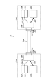
- the optical fiber power supply (PoF: Power over Fiber) system 1A of the present embodiment includes a power supply device (PSE: Power Sourcing Equipment) 110, an optical fiber cable 200A, and a power receiving device (PD: Powered Device) 310.
- PSE Power Sourcing Equipment
- PD Powered Device
- the power feeding device in the present disclosure is a device that converts electric power into light energy and supplies it
- a power receiving device is a device that receives the supply of light energy and converts the light energy into electric power.
- the power feeding device 110 includes a power feeding semiconductor laser 111.
- the optical fiber cable 200A includes an optical fiber 250A that forms a transmission line for feeding light.
- the power receiving device 310 includes a photoelectric conversion element 311.
- the power feeding device 110 is connected to a power source, and a power feeding semiconductor laser 111 or the like is electrically driven.
- the power feeding semiconductor laser 111 oscillates the laser with the electric power from the power source and outputs the power feeding light 112.
- one end 201A can be connected to the power feeding device 110, and the other end 202A can be connected to the power receiving device 310 to transmit the feeding light 112.
- the power feeding light 112 from the power feeding device 110 is input to one end 201A of the optical fiber cable 200A, the feeding light 112 propagates in the optical fiber 250A, and is output from the other end 202A to the power receiving device 310.
- the photoelectric conversion element 311 converts the feeding light 112 transmitted through the optical fiber cable 200A into electric power.
- the electric power converted by the photoelectric conversion element 311 is used as the driving power required in the power receiving device 310. Further, the power receiving device 310 can output the electric power converted by the photoelectric conversion element 311 for an external device.
- the semiconductor material constituting the semiconductor region that exerts the light-electric conversion effect of the power feeding semiconductor laser 111 and the photoelectric conversion element 311 is a semiconductor having a short wavelength laser wavelength of 500 nm or less. Since a semiconductor having a short wavelength laser wavelength has a large band gap and high photoelectric conversion efficiency, the photoelectric conversion efficiency on the power generation side and the power receiving side of optical power supply is improved, and the optical power supply efficiency is improved.
- the semiconductor material for example, a semiconductor material of a laser medium having a laser wavelength (fundamental wave) of 200 to 500 nm, such as diamond, gallium oxide, aluminum nitride, and GaN, may be used.
- a semiconductor having a band gap of 2.4 eV or more is applied as the semiconductor material.
- a semiconductor material of a laser medium having a bandgap of 2.4 to 6.2 eV such as diamond, gallium oxide, aluminum nitride, and GaN, may be used.
- a semiconductor material of a laser medium having a laser wavelength (fundamental wave) smaller than 200 nm may be used.
- These semiconductor materials may be applied to either one of the power feeding semiconductor laser 111 and the photoelectric conversion element 311. The photoelectric conversion efficiency on the power feeding side or the power receiving side is improved, and the optical power feeding efficiency is improved.
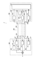
- the optical fiber power supply (PoF: Power over Fiber) system 1 of the present embodiment includes an optical power supply system via an optical fiber and an optical communication system, and includes a power supply device (PSE: Power Sourcing Equipment). It includes a first data communication device 100 including 110, an optical fiber cable 200, and a second data communication device 300 including a power receiving device (PD) 310.
- PSE Power Sourcing Equipment
- the power feeding device 110 includes a power feeding semiconductor laser 111.
- the first data communication device 100 includes a power supply device 110, a transmission unit 120 that performs data communication, and a reception unit 130.
- the first data communication device 100 corresponds to a data terminal equipment (DTE (Data Terminal Equipment)), a repeater (Repeater), and the like.
- the transmitter 120 includes a signal semiconductor laser 121 and a modulator 122.
- the receiving unit 130 includes a signal photodiode 131.
- the optical fiber cable 200 includes an optical fiber 250 having a core 210 forming a signal light transmission path and a clad 220 arranged on the outer periphery of the core 210 and forming a feeding light transmission path.
- the power receiving device 310 includes a photoelectric conversion element 311.
- the second data communication device 300 includes a power receiving device 310, a transmitting unit 320, a receiving unit 330, and a data processing unit 340.
- the second data communication device 300 is a power end station. Etc.
- the transmitter 320 includes a signal semiconductor laser 321 and a modulator 322.
- the receiving unit 330 includes a signal photodiode 331.
- the data processing unit 340 is a unit that processes a received signal.
- the second data communication device 300 is a node in the communication network. Alternatively, the second data communication device 300 may be a node that communicates with another node.
- the first data communication device 100 is connected to a power source, and a power feeding semiconductor laser 111, a signal semiconductor laser 121, a modulator 122, a signal photodiode 131, and the like are electrically driven.
- the first data communication device 100 is a node in the communication network.
- the first data communication device 100 may be a node that communicates with another node.
- the power feeding semiconductor laser 111 oscillates the laser with the electric power from the power source and outputs the power feeding light 112.
- the photoelectric conversion element 311 converts the power feeding light 112 transmitted through the optical fiber cable 200 into electric power.
- the electric power converted by the photoelectric conversion element 311 is the driving power of the transmitting unit 320, the receiving unit 330, and the data processing unit 340, and other driving power required in the second data communication device 300.
- the second data communication device 300 may be capable of outputting the electric power converted by the photoelectric conversion element 311 for an external device.
- the modulator 122 of the transmitting unit 120 modulates the laser light 123 from the signal semiconductor laser 121 based on the transmission data 124 and outputs it as the signal light 125.
- the signal photodiode 331 of the receiving unit 330 demodulates the signal light 125 transmitted through the optical fiber cable 200 into an electric signal and outputs it to the data processing unit 340.
- the data processing unit 340 transmits the data by the electric signal to the node, while receiving the data from the node and outputting the data as the transmission data 324 to the modulator 322.
- the modulator 322 of the transmitting unit 320 modulates the laser light 323 from the signal semiconductor laser 321 based on the transmission data 324 and outputs it as the signal light 325.
- the signal photodiode 131 of the receiving unit 130 demodulates the signal light 325 transmitted through the optical fiber cable 200 into an electric signal and outputs it.
- the data from the electrical signal is transmitted to the node, while the data from the node is referred to as transmission data 124.
- the feed light 112 and the signal light 125 from the first data communication device 100 are input to one end 201 of the optical fiber cable 200, the feed light 112 propagates through the clad 220, the signal light 125 propagates through the core 210, and the other end. It is output from 202 to the second data communication device 300.
- the signal light 325 from the second data communication device 300 is input to the other end 202 of the optical fiber cable 200, propagates through the core 210, and is output from one end 201 to the first data communication device 100.
- the first data communication device 100 is provided with an optical input / output unit 140 and an optical connector 141 attached to the optical input / output unit 140.
- the second data communication device 300 is provided with an optical input / output unit 350 and an optical connector 351 attached to the optical input / output unit 350.
- An optical connector 230 provided at one end 201 of the optical fiber cable 200 connects to the optical connector 141.
- An optical connector 240 provided at the other end 202 of the optical fiber cable 200 connects to the optical connector 351.
- the optical input / output unit 140 guides the feeding light 112 to the clad 220, guides the signal light 125 to the core 210, and guides the signal light 325 to the receiving unit 130.
- the optical input / output unit 350 guides the feeding light 112 to the power receiving device 310, guides the signal light 125 to the receiving unit 330, and guides the signal light 325 to the core 210.
- the optical fiber cable 200 has one end 201 connectable to the first data communication device 100 and the other end 202 connectable to the second data communication device 300 to transmit the feeding light 112. Further, in the present embodiment, the optical fiber cable 200 transmits the signal lights 125 and 325 in both directions.
- the semiconductor material constituting the semiconductor region that exhibits the light-electricity conversion effect of the power feeding semiconductor laser 111 and the photoelectric conversion element 311 As the semiconductor material constituting the semiconductor region that exhibits the light-electricity conversion effect of the power feeding semiconductor laser 111 and the photoelectric conversion element 311, the same materials as those in the first embodiment are applied, and high light power feeding efficiency is realized. ..
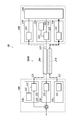
- the optical fiber 260 for transmitting signal light and the optical fiber 270 for transmitting the feeding light may be provided separately.
- the optical fiber cable 200B may also be composed of a plurality of cables.
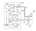
- FIG. 5 shows a configuration example (1) having a function of detecting a transmission failure of the feeding light in the above-mentioned optical fiber power feeding system 1
- FIG. 6 shows a state when a transmission failure occurs in the configuration example (1). ..
- the same reference numerals will be given to the configurations already described, and unless otherwise specified, the same configurations as those already described will be used.
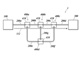
- the transmission path of the power supply light 112 is composed of a plurality of optical fiber cables 200a to 200g, and each optical fiber cable 200a to 200g is used for power supply. It is selectively connected by a plurality of connecting devices 400a to 400d including a switch 410.
- optical fiber cable 200 Since the optical fiber cables 200a to 200g have the same configuration except for their arrangement, they are abbreviated as "optical fiber cable 200" when it is not necessary to distinguish them (see FIG. 8). Similarly, since the connecting devices 400a to 400d have the same configuration except for the arrangement, they are abbreviated as “connecting device 400” when it is not necessary to distinguish them (see FIG. 8).
- the configuration example (1) having the transmission defect detection function it is sufficient that the first data communication device 100 and the second data communication device 300 can be connected by at least two or more transmission paths. Therefore, in this configuration example (1), a configuration in which seven optical fiber cables 200a to 200g are connected by four connecting devices 400a to 400d is illustrated, but the number of optical fiber cables 200 and connecting devices 400 can be increased or decreased. Is.
- optical fiber cables 200a, 200b, 200c, and 200d are connected in series between the first data communication device 100 and the second data communication device 300 via three connection devices 400a, 400b, and 400c. Have been placed. All optical switches 410 are provided with three ports for connecting the ends of the clad 220 of the optical fiber cable 200, and two of the three ports are connected so as to selectively transmit light. can do.
- the optical switches 410 of the respective connecting devices 400a, 400b, and 400c each use two ports to connect four optical fiber cables 200a to 200d in series. Further, one end of another optical fiber cable 200e to 200g is connected to the remaining one port of the optical switch 410 of each connection device 400a, 400b, 400c, and these three optical fiber cables 200e to 200g are connected to each other. The other end is individually connected to the three ports of the optical switch 410 of the connecting device 400d.
- the power supply optical fiber from the first data communication device 100 to the second data communication device 300 is supplied.
- the 112 is transmitted by the first transmission path consisting of the optical fiber cables 200a, 200b, 200c, 200d, the second transmission path consisting of the optical fiber cables 200a, 200e, 200g, 200c, 200d, and the optical fiber cables 200a, 200b, 200g. , 200f, 200d, and any of the fourth transmission path consisting of the optical fiber cables 200a, 200e, 200f, and 200d can be selectively configured.
- the power feeding optical fiber 112 can be transmitted by using another transmission path that bypasses the transmission failure (the fourth transmission path is illustrated in FIG. 6).
- the first data communication device 100 of the optical fiber power supply system 1 in the configuration example (1) having the transmission failure detection function detects the reflected light 112R of the power supply light 112 and bypasses the transmission failure location.
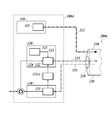
- a configuration for outputting a command to each optical switch 410 is added so that a transmission path is configured. That is, the first data communication device 100 is a beam that extracts the reflected light 112R of the feeding light 112 reflected at the transmission failure portion from one end of the clad 220 of the optical fiber cable 200a in which the feeding light 112 from the feeding semiconductor laser 111 is incident.
- the beam splitter 151 is arranged between the feeding semiconductor laser 111 and the optical fiber cable 200a, transmits the feeding light 112 from the feeding semiconductor laser 111 to the optical fiber cable 200a, and transmits the feeding light 112 from the optical fiber cable 200a to the feeding semiconductor laser 111.
- the reflected light 112R from the defective portion is reflected to the photoelectric conversion element 152 side.
- the photoelectric conversion element 152 is arranged so that the beam splitter 151 faces the reflected light 112R in the direction of reflection, and detects the light intensity of the incident reflected light 112R.
- the beam splitter 151 and the photoelectric conversion element 152 constitute a detection unit that detects the reflected light 112R of the feeding light 112 from a transmission failure portion generated in the transmission path of the feeding light 112.
- the control device 153 identifies a process of detecting the occurrence of a transmission failure and the distance to the transmission failure location by the detection signal of the photoelectric conversion element 152, and a transmission path that bypasses the transmission failure location by the detected distance to the transmission failure location. A process of outputting a command for switching the connection of each optical switch 410 is performed so that the power feeding light 112 is transmitted by the specified transmission path.
- the control device 153 may be composed of a microcomputer, or may be composed of a sequencer using an analog circuit or a digital circuit.
- the control device 153 includes a memory (not shown) that stores the threshold value of the detected light intensity of the photoelectric conversion element 152, and detects the occurrence of a transmission failure depending on whether or not the detected light intensity exceeds the stored threshold value.
- control device 153 calculates the distance from the first data communication device 100 to the transmission defective portion from the elapsed time from the emission of the feeding light 112 to the incident of the reflected light 112R by the output of the photoelectric conversion element 152. Can be done. Alternatively, the control device 153 may be configured to calculate the distance from the first data communication device 100 to the transmission defective portion from the phase difference between the feeding light 112 and the reflected light 112R by the output of the photoelectric conversion element 152.
- the first to fourth transmission paths can be selectively configured, and the control device 153 can be the first to the first.
- a predetermined port connection state is commanded and output to the optical switches 410 of the connection devices 400a to 400d.
- the control device 153 also selects a shorter transmission path. For example, when no transmission failure has occurred, the port connection state is simply output as a command so as to form a transmission path (for example, the first transmission path) having the shortest transmission distance.
- the port connection state is commanded and output so as to form a transmission path (for example, a fourth transmission path) having the shortest transmission distance among the transmission paths bypassing the transmission failure location. Therefore, the control device 153 stores the transmission distances of the first to fourth transmission paths. Further, the priority order of the first to fourth transmission paths may be determined in advance. Further, since the control device 153 always remembers which of the first to fourth transmission paths is currently configured, when the distance from the first data communication device 100 to the transmission failure location is obtained, It is possible to determine at which position on which transmission path a transmission failure has occurred. Thereby, it is possible to identify which optical fiber cable 200a to 200g has a transmission defect.
- control device 153 selects a transmission path that does not include the optical fiber cable 200 in which the transmission failure has occurred from the first to fourth transmission paths. Then, the control device 153 individually commands the optical switches 410 of the connection devices 400a to 400d to be in an appropriate port connection state so that the selected transmission path is configured.
- the command of the port connection state to the optical switches 410 of the connection devices 400a to 400d may be transmitted by connecting a communication cable capable of transmitting an electric signal to each optical switch 410.
- the command of the port connection state for each optical switch 410 is included in the signal light 125 output from the transmitting unit 120, and the optical switches 410 of the connecting devices 400a to 400d are included in the core 210 of each optical fiber cable 200.
- the configuration to be propagated to is illustrated.
- the control device 153 controls the modulator 122 of the transmitting unit 120 to modulate the laser light 123 from the signal semiconductor laser 121 based on the command of the port connection state to each optical switch 410 and output it as the signal light 125.
- the signal light 125 is output by being modulated so as to include the destination information indicating which connection device 400a to 400d is the command and the control information indicating the port connection state.
- the second data communication device 300 and each connection device 400 can distinguish the transmission information to the second data communication device 300 or another node and the command to each optical switch 410, and the second data. Appropriate communication can be performed between the communication device 300 and each connection device 400.
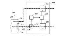
- FIG. 8 is a block diagram showing the configuration of each connection device 400.
- Each connecting device 400 includes the above-mentioned optical switch 410 for power feeding that switches the optical path of the feeding light 112, the optical switch 420 for the signal that switches the optical path of the signal lights 125 and 325, and a signal from the end of the optical fiber cable 200.
- Optical switches 410 and 420 based on the detection of a beam splitter 431 that extracts a part of the light 125, a signal photodiode 432 that receives a part of the signal light 125 extracted by the beam splitter 431, and a signal photodiode 432. It is provided with a control device 433 that controls to switch the port connection state (which of the three ports is connected).
- the beam splitter 431 is arranged so that the signal lights 125 and 325 propagating through the core of the optical fiber cable 200 are transmitted. Then, the signal light 325 from the beam splitter 431 to the fiber optic cable 200 is transmitted, a part of the signal light 125 from the fiber optic cable 200 to the beam splitter 431 is reflected to the signal photodiode side, and the remaining part is transmitted.
- the reflectance of the beam splitter 431 may be equal to or greater than the minimum range in which the information contained in the reflected signal light 125 can be read by the signal photodiode 432.
- the signal photodiode 432 is arranged so that the beam splitter 431 faces the direction in which the signal light 125 is reflected, and the incident signal light 125 is demodulated into an electric signal and output.
- the control device 433 reads the electrical signal output from the signal photodiode 432 when it contains the above-mentioned destination information and control information. Then, it is determined whether the destination indicated by the destination information is the own connection device 400 or another connection device 400, and if it is itself, the port connection state included in the control information is obtained.
- the optical switch 410 for power supply and the optical switch 420 for signal are switched. Further, when the electric signal output from the signal photodiode 432 does not include the destination information and the control information, or when the destination indicated by the destination information is another connection device 400, the control device 433 may be used. , Maintain the current port connection status.
- the control device 433 may be composed of a microcomputer, or may be composed of a sequencer using an analog circuit or a digital circuit.
- the optical switch 420 for signals like the optical switch 410 for power supply, has three ports for connecting the ends of the core 210 of the optical fiber cable 200, and selectively selects two of the three ports. Can be connected so that optical transmission is possible.
- the optical switch 410 for power supply and the optical switch 420 for signal are both controlled by the control device 433 so as to connect the same optical fiber cables 200 to each other.
- the connecting device 400 may be provided with a photoelectric conversion element that receives a part of the feeding light 112, and a configuration for supplying power to each configuration of the connecting device 400 may be added. As a result, each connecting device 400 can eliminate the need for a power supply.
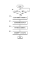
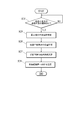
- FIG. 9 is a flowchart showing a process at the time of detecting a transmission failure of the feeding light 112 executed by the control device 153 of the first data communication device 100.
- the control device 153 compares the detected light intensity of the reflected light 112R of the feeding light 112 received by the photoelectric conversion element 152 with the threshold value stored in advance at the time of feeding (step S1). Then, when the detected light intensity of the reflected light 112R does not exceed the threshold value, the comparison with the threshold value is repeatedly executed.
- the control device 153 determines that a transmission failure has occurred, and from the output of the photoelectric conversion element 152, from the first data communication device 100 The distance to the transmission defective portion is calculated (step S2).
- control device 153 stores a command for switching the port connection state last output to the optical switch 410 of each connection device 400, and the current transmission path is any of the first to fourth transmission paths. It is possible to specify whether it is configured. Further, the distance from the first data communication device 100 calculated in step S2 to the transmission failure location is used to identify at which position (which optical fiber cable 200) the transmission failure is occurring on the current transmission path. (Step S3).
- the control device 153 selects and determines a transmission path capable of bypassing the position of the specified transmission defective portion from the first to fourth transmission paths (step S4). Then, a port connection state command including transmission destination information and control information is sent to the signal light 125 of the transmission unit 120 to the optical switches 410 of the connection devices 400a to 400d so that the selected transmission path is configured. It is included and transmitted (step S5), and the process ends.
- the processes of steps S1 to S5 are repeatedly executed in a short cycle.
- each of the connecting devices 400a to 400d receives the signal light 125 by the signal photodiode 432, demodulates it into an electric signal, and reads the transmission destination information and the control information. Then, each of the connecting devices 400a to 400d controls to appropriately switch the port connection state of each optical switch 410, and constitutes a transmission path capable of bypassing the position of the transmission defective portion.
- the optical fiber power feeding system 1 of the configuration example (1) having the transmission failure detection function As described above, in the optical fiber power feeding system 1 of the configuration example (1) having the transmission failure detection function, the distance from the reflected light 112R of the feeding light 112 to the transmission defective part is obtained, and the other feeding light bypassing the transmission defective part is obtained.
- the optical switches 410 of the plurality of connecting devices 400 are controlled so as to form the transmission path of 112. Therefore, even if a transmission failure occurs in a certain power feeding light transmission path, the feeding light 112 can be bypassed and transmitted in a new transmission path. As a result, even if a state in which the feeding light 112 cannot be transmitted occurs due to a transmission failure location, it can be quickly recovered and power can be supplied with higher efficiency.
- each optical fiber is utilized by utilizing the communication function provided in the optical fiber power feeding system 1 by controlling the optical switches 410 of the plurality of connecting devices 400 by the signal light 125 through the optical fiber cable 200. It becomes possible to control the switch 410. Therefore, it is possible to avoid the complexity of the system and construct the system with a small amount of resources.
- control device 153 controls a plurality of optical switches 410 so as to preferentially configure the transmission path of the feeding light having a shorter transmission distance, so that the feeding light 112 is transmitted. It is possible to minimize the loss.
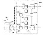
- FIG. 10 is a block diagram showing the configuration of each connection device 400A.
- Each connecting device 400A includes the above-mentioned optical switch 410 for feeding that switches the optical path of the feeding light 112, the optical switch 420 for the signal that switches the optical path of the signal lights 125 and 325 and other signal lights described later, and light.
- a control device 433A that controls switching between switches 410 and 420, a beam splitter 451A that extracts a part of signal light 125, 325 and other signal light (hereinafter referred to as signal light) from the end of the optical fiber cable 200, and a beam. It is provided with a signal photodiode 452A that receives a part of signal light or the like taken out by the splitter 451A.
- each connection device 400A includes a beam splitter 431A that takes out a part of the feeding light 112 from the end of the optical fiber cable 200, a photoelectric conversion element 432A that receives a part of the feeding light 112 taken out by the beam splitter 431A, and so on. It is provided with a signal semiconductor laser 443A, a modulator 442A that modulates the laser light under the control of the control device 433A, and a beam splitter 441A that outputs other modulated signal light on the same transmission path as the signal lights 125 and 325. There is.
- the beam splitter 431A and the photoelectric conversion element 432A constitute a detection unit for detecting a transmission failure state of the feeding light 112.
- the beam splitter 431A takes out a part of the feeding light 112 in the middle of the transmission path and inputs it to the photoelectric conversion element 432A.
- the photoelectric conversion element 432A detects the light intensity of a part of the input feeding light 112 and inputs it to the control device 433A.
- the photoelectric conversion element 432A may be provided with a configuration in which power is supplied to each configuration of the connecting device 400A by incident light of the feeding light 112. As a result, the power supply can be eliminated from each connection device 400A.
- the beam splitter 451A takes out a part of the signal light or the like toward the first data communication device 100 side and a part of the signal light or the like toward the second data communication device 300 side and inputs it to the signal photodiode 452A. ..
- the signal photodiode 452A demodulates the signal light or the like input from the beam splitter 451A into an electric signal and inputs it to the control device 433A.
- the signal semiconductor laser 443A outputs a laser beam, is modulated by the modulator 442A controlled by the control device 433A, becomes another signal light, and is input to the beam splitter 441A.
- the beam splitter 441A transmits other signal lights to the first data communication device 100 side and the second data communication device 300 side on the same transmission path as the signal lights 125 and 325.
- the signal semiconductor laser 443A, the modulator 442A, and the beam splitter 441A form an output unit that outputs the detection result of the detection unit to the outside.
- the control device 433A determines the presence or absence of a transmission failure state of the feed light 112 from the light intensity of the feed light 112 and outputs the determination result to the outside, and the presence or absence of a transmission failure state from each connection device 400A. Based on the determination result, the second process of outputting a port connection status command to the optical switch 410 of each connection device 400A to configure a transmission path that bypasses the transmission failure location, and optical according to the port connection status command. A third process for controlling the port connection of the switches 410 and 420 is executed.
- the control device 433A may be composed of a microcomputer, or may be composed of a sequencer using an analog circuit or a digital circuit.
- the control device 433A determines the feeding light 112 on the upstream side (first data communication device 100 side) of the connecting device 400A from the light intensity of the feeding light 112 detected by the photoelectric conversion element 432A. Determine if there is a transmission failure state. That is, when a transmission failure state occurs on the upstream side of the connecting device 400A, the detected light intensity of the feeding light 112 is lowered. Therefore, the control device 433A is provided with a storage unit having a predetermined threshold value, and the presence or absence of a transmission failure state can be determined by comparing the threshold value with the detected light intensity of the feeding light 112.
- control device 433A forms another signal light through the signal semiconductor laser 443A and the modulator 442A, and outputs the determination result to the outside (other connection devices 400A, first and second data communication devices 100, 300). To do.
- the control device 433A includes the transmission source information indicating which connection device 400A has made the determination and the determination result information in the other signal light and outputs the determination to the outside.
- the other connecting devices 400A and the first and second data communication devices 100 and 300 that have received the other signal light are in a normal state or a transmission failure state in a range upstream of the specific connecting device 400A. You can recognize if there is.
- control device 433A acquires the determination result information of the connecting device 400A other than the own device from the other signal light from the connecting device 400A of the other device for the second processing. That is, the control device 433A receives the determination result information from all the other connecting devices 400A constituting any of the first to fourth transmission paths currently selected through the signal photodiode 452A, and receives itself. Collect all judgment result information including the machine. Then, in the control device 433, the optical fiber cable 200 connected to the upstream side of the most upstream connection device 400A whose determination result is in the transmission failure state is transmitted among all the connection devices 400A constituting the current transmission path. It can be identified as a defective part.
- the control device 433A selects a transmission path that does not include the optical fiber cable 200 from the first to fourth transmission paths. It is preferable that the control device 433A is configured to preferentially select a transmission path having a shorter path length at all times, regardless of whether or not a transmission failure has occurred. Further, the priority order of the first to fourth transmission paths may be determined in advance.
- the feeding light 112, signal light, etc. may be completely cut off.
- the connection device 400A included in the current transmission path cannot obtain another signal light including the determination result information.
- the connection device 400A is subjected to a process of assuming that it is in a transmission failure state. This makes it possible to identify the optical fiber cable 200, which is a transmission failure location.
- control device 433A of the optical switch 410 of each connection device 400a to 400d (see FIG. 5, in which each connection device 400a to 400d has the same configuration as the connection device 400A) in order to configure the selected transmission path. Outputs a command to switch the port connection status (which of the three ports is connected). That is, the control device 433A forms another signal light through the signal semiconductor laser 443A and the modulator 442A, and issues the command of the port connection state to the outside (other connection devices 400A, first and second data communication devices 100, Output to 300).
- control device 433A self-generates a port connection state command for constructing a transmission path bypassing a transmission defective portion for the third process, or for a signal from another connection device 400A.
- a command of a port connection state for forming a transmission path bypassing a transmission defective portion is received through the photodiode 452A, control for switching the port connection of the optical switches 410 and 420 is executed according to the command.
- the control device 433A executes the control of switching the port connection of the optical switches 410 and 420 according to the command of the port connection state for forming the transmission path bypassing the transmission defective part.
- a transmission path that bypasses the defective transmission portion is configured.
- the control devices 433A of the plurality of connecting devices 400A identify the optical fiber cable 200 in which the transmission failure has occurred, select the transmission path that bypasses the transmission failure location, and configure the transmission path.
- the command of the port connection state to do so will be sent to the outside.
- the port connection state for configuring the transmission path bypassing the transmission defective portion output by each connecting device 400A Since the command of is the same, it is possible to properly configure a transmission path that bypasses the transmission failure location.
- FIG. 11 is a flowchart showing a process (first process) at the time of detecting a transmission failure of the feeding light 112 executed by the control device 433A of each connecting device 400A. This process is always repeated in a short cycle.
- the control device 433A detects the light intensity of a part of the feeding light 112 received by the photoelectric conversion element 432A at the time of feeding (step S11), and compares the detected light intensity with the threshold value stored in advance. (Step S13).
- the control device 433A forms another signal light through the signal semiconductor laser 443A and the modulator 442A, and the source information indicating its own device. And the determination result information indicating that the transmission of the feeding light 112 is normal is included and output to the outside (step S15). Further, when the detected light intensity of some of the feeding light 112 does not reach the threshold value, the control device 433A provides the signal light with source information and determination result information indicating that the feeding light 112 is in a transmission failure state. It is included and output to the outside (step S17).
- FIG. 12 is a flowchart showing a process (second process) for forming a transmission path bypassing a transmission failure portion of the feeding light 112 executed by the control device 433 of each connection device 400A.
- the control device 433A of each connection device 400A acquires the transmission source information and the determination result information output from the other connection device 400A through the signal photodiode 452A. Then, it is determined whether or not there is a transmission defect by referring to the determination result information of all the connection devices 400A included in the current transmission path (step S21). At this time, the connection device 400A for which the source information and the determination result information cannot be obtained is regarded as a transmission failure.
- step S21 If the connection device 400A with poor transmission does not exist, the process of step S21 is repeatedly executed, and if the connection device 400A with poor transmission exists, the most upstream side (first data communication device side) among them.
- the connection device 400A to be used is specified (step S23). Then, the optical fiber cable 200 connected to the upstream side of the connection device 400A on the most upstream side is identified as a transmission failure location (step S25).
- control device 433A selects a transmission path that does not pass through the optical fiber cable 200, which is a transmission failure location, from the four transmission paths, and if necessary, can be bypassed in consideration of the transmission distance, priority, and the like.
- One transmission path is determined (step S27).
- a command for switching the port connection state of the optical switches 410 of the connection devices 400a to 400d is output to the outside through the signal semiconductor laser 443A and the modulator 442A in order to configure the determined transmission path (step S29).
- each connection device 400A receives a command for switching the port connection state from the plurality of other connection devices 400A through the signal photodiode 452A, but the control device 433A of each connection device 400A has a common algorithm. Since the transmission path is determined by, the command with the same content is received. Therefore, follow either directive. For example, when the control device 433A includes the determination result information in the signal light and transmits the determination result information, the determination time information is also included, and a command for switching the port connection state from a plurality of other connection devices 400A is received. In addition, the control device 433A may be configured to follow the latest determination result information including the command of the own machine.
- the control device 433A may perform a confirmation process for determining whether or not these commands are the same. In that case, if they are the same, the next process may be advanced, and if they are not the same, a process of notifying each connection device 400A of an error may be performed assuming that some abnormality has occurred.
- control device 433A extracts a command for the optical switches 410 and 420 of its own connection device 400A from the commands for switching the port connection state, and connects the ports of the optical switches 410 and 420 according to the command.
- each of the connecting devices 400a to 400d controls to appropriately switch the port connection state of each optical switch 410, and constitutes a transmission path capable of bypassing the position of the transmission defective portion.
- the connection device 400A serves as a detection unit for detecting the transmission failure state of the power supply light 112 and an output unit for outputting the detection result to the outside.
- the control device 433A identifies a transmission failure location according to the detection result of the transmission failure status of the plurality of connection devices 400A, and configures another power feeding light transmission path that bypasses the transmission failure location. It outputs a command to switch the port connection state to control the optical switches of the plurality of connection devices 400A. Therefore, even if a transmission failure occurs in a certain power feeding light transmission path, the feeding light 112 can be bypassed and transmitted in a new transmission path. As a result, even if a state in which the feeding light 112 cannot be transmitted occurs due to a transmission failure location, it can be quickly recovered and power can be supplied with higher efficiency.
- each connection device 400A detects a transmission failure state from the light intensity of the power feeding light 112, so that a transmission failure can be stably detected by a simple configuration.
- each optical switch 410 is operated by utilizing the communication function provided in the optical fiber power supply system 1. It becomes possible to control. Therefore, it is possible to avoid the complexity of the system and construct the system with a small amount of resources.
- a control device 433A for controlling the optical switches 410 of the plurality of connecting devices 400A so as to form a transmission path of another power feeding light bypassing the transmission defective portion is connected to include the optical switch 410. Since it is provided in the device 400A, even if a transmission failure occurs and communication becomes difficult, the connecting device 400A can autonomously judge and at least only the optical switch 410 of its own unit can be operated properly. It will be possible. Further, in the optical fiber power supply system 1, when all the connecting devices 400A are configured to include the control device 433A, all the connecting devices 400A can autonomously switch the optical switch 410, resulting in transmission failure. Even if mutual communication becomes difficult, a bypass transmission path can be configured, recovery can be performed more appropriately, and system reliability can be improved.
- the control device 433 of each connection device 400A outputs the determination result of the presence / absence of the transmission failure state to the outside, and the transmission.
- the second process may be configured by the first data communication device 100.
- a configuration example (3) having a transmission defect detection function in which the first data communication device 100 includes the control device 153A that performs the second process will be described with reference to the block diagram of FIG.
- the above description is made except that the first data communication device 100A includes the control device 153A and the control device 433 of each connection device 400A does not perform the second processing.
- the configuration is the same as that of the configuration example (2) having the transmission defect detection function of the optical fiber power supply system 1.
- the first data communication device 100A is the same as the first data communication device 100 of the configuration example (2) except that the control device 153A is provided.
- the control device 153A of the first data communication device 100A outputs the source information of each connection device 400A included in the other signal light from the signal photodiode 131 of the receiving unit 130 and the determination result information indicating the presence or absence of a transmission defect. Can be obtained. Then, as the second process, the control device 153A transmits the determination result information from all the connecting devices 400A constituting any of the currently selected first to fourth transmission paths through the signal photodiode 131. collect. Further, in the control device 153A, the optical fiber cable 200 connected to the upstream side of the most upstream connection device 400A whose determination result is in a transmission failure state is transmitted among all the connection devices 400A constituting the current transmission path.
- a transmission path that does not include the optical fiber cable 200 in which the transmission failure has occurred is selected in consideration of the shortness of the path length and the priority of each layer path by identifying the defective portion.
- the control device 153A uses a command for switching the port connection state of the optical switches 410 of the connection devices 400a to 400d as other communication light in order to control the modulator 122 of the transmission unit 120 and configure the selected transmission path. Output and transmit to each connection device 400A. In this way, the control device 153A indirectly controls each optical switch 410 by transmitting a command for switching the port connection state of the optical switch 410 to the connection devices 400a to 400d constituting the selected transmission path. It can be said that there is.
- the control device 153A may be composed of a microcomputer, or may be composed of a sequencer using an analog circuit or a digital circuit.
- control device 153A that performs the second processing when the control device 153A that performs the second processing is provided in the first data communication device 100A, it is not necessary to perform the second processing in each connection device 400A, so that the system configuration is simplified. It becomes possible.
- the command to switch the port connection state is output only from the first data communication device 100A, not from each connection device 400A, it is possible to reduce congestion during communication and maintain good communication. Become.
- the second process performed by the control device 433A of the configuration example (2) having the transmission defect detection function of the optical fiber power supply system 1 described above is performed by the data processing unit 340 as the control device of the second data communication device 300. May be.
- the optical fiber power supply system 1 is the same as the configuration example (2) except that the control device 433A of each connection device 400A does not perform the second process.
- the configuration of the second data communication device 300 is the same as the configuration of FIG. 2 except for the processing performed by the data processing unit 340.
- the data processing unit 340 of the second data communication device 300 has source information of each connection device 400A included in other signal light from the signal photodiode 331 of the reception unit 330, and determination result information indicating the presence or absence of a transmission defect. Is obtained, the optical fiber cable 200 in a transmission failure state is identified, and a transmission path for bypassing the optical fiber cable 200 is selected. Then, the data processing unit 340 controls the modulator 322 of the transmission unit 320 to issue a command to switch the port connection state of the optical switches 410 of the connection devices 400a to 400d in order to configure the selected transmission path. Is output as, and is transmitted to each connecting device 400A. In this case as well, the data processing unit 340 indirectly controls each optical switch 410 by transmitting a command for switching the port connection state of the optical switch 410 to the connection devices 400a to 400d constituting the selected transmission path. It can be said that it is.
- the configuration examples (1) to (4) having the transmission defect detection function an example in which the configuration having the transmission defect detection function is applied to the optical fiber power supply system 1 is shown.
- the functional configuration can also be applied to the optical fiber power supply system 1B.
- control devices 433 of all the connection devices 400 execute the second process, but only the control devices 433 of some connection devices 400 are used. It may be configured to execute the second process. In this case, it is preferable that the control device 433 of the connecting device 400a or 400c included in all the first to fourth transmission paths of the feeding light 112 executes the second process. Further, it is more preferable that the control device 433 of the connecting device 400a located on the upstream side executes the second process.
- the configuration having the transmission defect detection function is supplied with power from one first data communication device 100 to one second data communication device 300.
- An example of application to the optical fiber power supply system 1 to be performed is shown, but the present invention is not limited to this.
- it may be applied to an optical fiber power feeding system that supplies power from one first data communication device 100 to a plurality of second data communication devices 300. In that case, since the transmission path of the feeding light 112 is formed by branching from the first data communication device 100 to the plurality of second data communication devices 300, the feeding light for one second data communication device 300 is formed.
- the transmission path of the feeding light 112 to the other second data communication device 300 can be bypassed, and it is necessary to prepare a dedicated transmission path for bypassing. It is possible to simplify the configuration and save resources.
- the optical power supply system according to the present invention has industrial applicability for an optical power supply system that stably supplies power.
- Optical fiber power supply system 100, 100A First data communication device 110 Power supply device 111 Power supply semiconductor laser 112 Power supply light 112R Reflected light 120 Transmitter 121 Signal semiconductor laser 122 Modulator 123 Laser light 124 Transmission data 125 Signal light 130 Receiver 131 Signal photodiode 140 Optical input / output section 141 Optical connector 151 Beam splitter (detector) 151A control device 152 photoelectric conversion element (detector) 153 Control device 200, 200A, 200B, 200a to 200g Optical fiber cable 210 Core 220 Clad 230, 240 Optical connector 250, 250A, 260, 270 Optical fiber 300 Second data communication device 310 Power receiving device 311 Photodiode conversion element 320 Transmitter 321 Signal Semiconductor laser 322 Modulator 323 Laser light 324 Transmission data 325 Signal light 330 Receiver 331 Signal photodiode 340 Data processing unit 350 Optical input / output unit 351 Optical input / output
Landscapes
- Physics & Mathematics (AREA)
- Engineering & Computer Science (AREA)
- Computer Networks & Wireless Communication (AREA)
- Electromagnetism (AREA)
- Signal Processing (AREA)
- Optics & Photonics (AREA)
- Power Engineering (AREA)
- General Physics & Mathematics (AREA)
- Optical Communication System (AREA)
Abstract
光給電効率の向上を図るために、本発明の光ファイバー給電システムは、電力によりレーザー発振して給電光を出力する半導体レーザーを含む給電装置110と、給電光を電力に変換する光電変換素子311を含む受電装置310と、給電光を伝送する複数の光ファイバーケーブル200a~200gと、複数の光ファイバーケーブルを選択的に接続する複数の光スイッチ410とを備え、複数の光ファイバーケーブルと複数の光スイッチとにより、少なくとも二以上の給電光の伝送経路が構成可能であり、給電光の伝送経路に生じた伝送不良箇所を検出する検出部151、152と、検出部が検出した伝送不良箇所に応じて、当該伝送不良箇所を迂回する他の給電光の伝送経路を構成するように複数の光スイッチを制御する制御装置153とを備える構成とした。
Description
本開示は、光ファイバー給電システムに関する。
近時、電力を光(給電光と呼ばれる)に変換して伝送し、当該給電光を電気エネルギーに変換して電力として利用する光給電システムが研究されている。
特許文献1には、電気信号で変調された信号光、及び電力を供給するための給電光を発信する光発信機と、上記信号光を伝送するコア、上記コアの周囲に形成され上記コアより屈折率が小さく上記給電光を伝送する第1クラッド、及び上記第1クラッドの周囲に形成され上記第1クラッドより屈折率が小さい第2クラッド、を有する光ファイバーと、上記光ファイバーの第1クラッドで伝送された上記給電光を変換した電力で動作し、上記光ファイバーのコアで伝送された上記信号光を上記電気信号に変換する光受信機と、を備えた光通信装置が記載されている。
特許文献1には、電気信号で変調された信号光、及び電力を供給するための給電光を発信する光発信機と、上記信号光を伝送するコア、上記コアの周囲に形成され上記コアより屈折率が小さく上記給電光を伝送する第1クラッド、及び上記第1クラッドの周囲に形成され上記第1クラッドより屈折率が小さい第2クラッド、を有する光ファイバーと、上記光ファイバーの第1クラッドで伝送された上記給電光を変換した電力で動作し、上記光ファイバーのコアで伝送された上記信号光を上記電気信号に変換する光受信機と、を備えた光通信装置が記載されている。
光給電においては、より一層の光給電効率の向上が求められている。そのための一つとして、給電側及び受電側における光電変換効率の向上が求められている。
本開示の1つの態様の光ファイバー給電システムは、
電力によりレーザー発振して給電光を出力する半導体レーザーを含む給電装置と、
前記給電光を電力に変換する光電変換素子を含む受電装置と、
前記給電光を伝送する複数の光ファイバーケーブルと、
複数の前記光ファイバーケーブルを選択的に接続する複数の光スイッチとを備え、
複数の前記光ファイバーケーブルと複数の前記光スイッチとにより、少なくとも二以上の前記給電光の伝送経路が構成可能であり、
前記給電光の伝送経路に生じた伝送不良箇所からの前記給電光の反射光を検出する検出部と、
前記検出部が検出した前記反射光から前記伝送不良箇所までの距離を求め、当該伝送不良箇所を迂回する他の前記給電光の伝送経路を構成するように複数の前記光スイッチを制御する制御装置と、を備えている。
電力によりレーザー発振して給電光を出力する半導体レーザーを含む給電装置と、
前記給電光を電力に変換する光電変換素子を含む受電装置と、
前記給電光を伝送する複数の光ファイバーケーブルと、
複数の前記光ファイバーケーブルを選択的に接続する複数の光スイッチとを備え、
複数の前記光ファイバーケーブルと複数の前記光スイッチとにより、少なくとも二以上の前記給電光の伝送経路が構成可能であり、
前記給電光の伝送経路に生じた伝送不良箇所からの前記給電光の反射光を検出する検出部と、
前記検出部が検出した前記反射光から前記伝送不良箇所までの距離を求め、当該伝送不良箇所を迂回する他の前記給電光の伝送経路を構成するように複数の前記光スイッチを制御する制御装置と、を備えている。
以下に本開示の一実施形態につき図面を参照して説明する。
(1)システム概要
〔第1実施形態〕
図1に示すように本実施形態の光ファイバー給電(PoF:Power over Fiber)システム1Aは、給電装置(PSE:Power Sourcing Equipment)110と、光ファイバーケーブル200Aと、受電装置(PD:Powered Device)310を備える。
なお、本開示における給電装置は電力を光エネルギーに変換して供給する装置であり、受電装置は光エネルギーの供給を受け当該光エネルギーを電力に変換する装置である。
給電装置110は、給電用半導体レーザー111を含む。
光ファイバーケーブル200Aは、給電光の伝送路を形成する光ファイバー250Aを含む。
受電装置310は、光電変換素子311を含む。
〔第1実施形態〕
図1に示すように本実施形態の光ファイバー給電(PoF:Power over Fiber)システム1Aは、給電装置(PSE:Power Sourcing Equipment)110と、光ファイバーケーブル200Aと、受電装置(PD:Powered Device)310を備える。
なお、本開示における給電装置は電力を光エネルギーに変換して供給する装置であり、受電装置は光エネルギーの供給を受け当該光エネルギーを電力に変換する装置である。
給電装置110は、給電用半導体レーザー111を含む。
光ファイバーケーブル200Aは、給電光の伝送路を形成する光ファイバー250Aを含む。
受電装置310は、光電変換素子311を含む。
給電装置110は電源に接続され、給電用半導体レーザー111等が電気駆動される。
給電用半導体レーザー111は、上記電源からの電力によりレーザー発振して給電光112を出力する。
給電用半導体レーザー111は、上記電源からの電力によりレーザー発振して給電光112を出力する。
光ファイバーケーブル200Aは、一端201Aが給電装置110に接続可能とされ、他端202Aが受電装置310に接続可能とされ、給電光112を伝送する。
給電装置110からの給電光112が、光ファイバーケーブル200Aの一端201Aに入力され、給電光112は光ファイバー250A中を伝搬し、他端202Aから受電装置310に出力される。
給電装置110からの給電光112が、光ファイバーケーブル200Aの一端201Aに入力され、給電光112は光ファイバー250A中を伝搬し、他端202Aから受電装置310に出力される。
光電変換素子311は、光ファイバーケーブル200Aを通して伝送されてきた給電光112を電力に変換する。光電変換素子311により変換された電力が、受電装置310内で必要な駆動電力とされる。さらに受電装置310は光電変換素子311により変換された電力を外部機器用に出力可能とされる。
給電用半導体レーザー111及び光電変換素子311の光‐電気間の変換効果を奏する半導体領域を構成する半導体材料が500nm以下の短波長のレーザー波長をもった半導体とされる。
短波長のレーザー波長をもった半導体は、バンドギャップが大きく光電変換効率が高いので、光給電の発電側及び受電側における光電変換効率が向上され、光給電効率が向上する。
そのためには、同半導体材料として、例えば、ダイヤモンド、酸化ガリウム、窒化アルミニウム、GaN等、レーザー波長(基本波)が200~500nmのレーザー媒体の半導体材料を用いてもよい。
また、同半導体材料として、2.4eV以上のバンドギャップを有した半導体が適用される。
例えば、ダイヤモンド、酸化ガリウム、窒化アルミニウム、GaN等、バンドギャップ2.4~6.2eVのレーザー媒体の半導体材料を用いてもよい。
なお、レーザー光は長波長ほど伝送効率が良く、短波長ほど光電変換効率が良い傾向にある。したがって、長距離伝送の場合には、レーザー波長(基本波)が500nmより大きいレーザー媒体の半導体材料を用いてもよい。また、光電変換効率を優先する場合には、レーザー波長(基本波)が200nmより小さいレーザー媒体の半導体材料を用いてもよい。
これらの半導体材料は、給電用半導体レーザー111及び光電変換素子311のいずれか一方に適用してもよい。給電側又は受電側における光電変換効率が向上され、光給電効率が向上する。
短波長のレーザー波長をもった半導体は、バンドギャップが大きく光電変換効率が高いので、光給電の発電側及び受電側における光電変換効率が向上され、光給電効率が向上する。
そのためには、同半導体材料として、例えば、ダイヤモンド、酸化ガリウム、窒化アルミニウム、GaN等、レーザー波長(基本波)が200~500nmのレーザー媒体の半導体材料を用いてもよい。
また、同半導体材料として、2.4eV以上のバンドギャップを有した半導体が適用される。
例えば、ダイヤモンド、酸化ガリウム、窒化アルミニウム、GaN等、バンドギャップ2.4~6.2eVのレーザー媒体の半導体材料を用いてもよい。
なお、レーザー光は長波長ほど伝送効率が良く、短波長ほど光電変換効率が良い傾向にある。したがって、長距離伝送の場合には、レーザー波長(基本波)が500nmより大きいレーザー媒体の半導体材料を用いてもよい。また、光電変換効率を優先する場合には、レーザー波長(基本波)が200nmより小さいレーザー媒体の半導体材料を用いてもよい。
これらの半導体材料は、給電用半導体レーザー111及び光電変換素子311のいずれか一方に適用してもよい。給電側又は受電側における光電変換効率が向上され、光給電効率が向上する。
〔第2実施形態〕
図2に示すように本実施形態の光ファイバー給電(PoF:Power over Fiber)システム1は、光ファイバーを介した光給電システムと光通信システムとを含むものであり、給電装置(PSE:Power Sourcing Equipment)110を含む第1のデータ通信装置100と、光ファイバーケーブル200と、受電装置(PD:Powered Device)310を含む第2のデータ通信装置300とを備える。
なお、以下の説明では、原則として、既に説明された構成については同一の符号を付して、特に言及がない場合には既に説明された構成と同一の構成とする。
給電装置110は、給電用半導体レーザー111を含む。第1のデータ通信装置100は、給電装置110のほか、データ通信を行う発信部120と、受信部130とを含む。第1のデータ通信装置100は、データ端末装置(DTE(Data Terminal Equipment))、中継器(Repeater)等に相当する。発信部120は、信号用半導体レーザー121と、モジュレーター122とを含む。受信部130は、信号用フォトダイオード131を含む。
図2に示すように本実施形態の光ファイバー給電(PoF:Power over Fiber)システム1は、光ファイバーを介した光給電システムと光通信システムとを含むものであり、給電装置(PSE:Power Sourcing Equipment)110を含む第1のデータ通信装置100と、光ファイバーケーブル200と、受電装置(PD:Powered Device)310を含む第2のデータ通信装置300とを備える。
なお、以下の説明では、原則として、既に説明された構成については同一の符号を付して、特に言及がない場合には既に説明された構成と同一の構成とする。
給電装置110は、給電用半導体レーザー111を含む。第1のデータ通信装置100は、給電装置110のほか、データ通信を行う発信部120と、受信部130とを含む。第1のデータ通信装置100は、データ端末装置(DTE(Data Terminal Equipment))、中継器(Repeater)等に相当する。発信部120は、信号用半導体レーザー121と、モジュレーター122とを含む。受信部130は、信号用フォトダイオード131を含む。
光ファイバーケーブル200は、信号光の伝送路を形成するコア210と、コア210の外周に配置され、給電光の伝送路を形成するクラッド220と有する光ファイバー250を含む。
受電装置310は、光電変換素子311を含む。第2のデータ通信装置300は、受電装置310のほか、発信部320と、受信部330と、データ処理ユニット340とを含む。第2のデータ通信装置300は、パワーエンドステーション(Power End Station)
等に相当する。発信部320は、信号用半導体レーザー321と、モジュレーター322とを含む。受信部330は、信号用フォトダイオード331を含む。データ処理ユニット340は、受信した信号を処理するユニットである。また、第2のデータ通信装置300は、通信ネットワークにおけるノードである。または第2のデータ通信装置300は、他のノードと通信するノードでもよい。
等に相当する。発信部320は、信号用半導体レーザー321と、モジュレーター322とを含む。受信部330は、信号用フォトダイオード331を含む。データ処理ユニット340は、受信した信号を処理するユニットである。また、第2のデータ通信装置300は、通信ネットワークにおけるノードである。または第2のデータ通信装置300は、他のノードと通信するノードでもよい。
第1のデータ通信装置100は電源に接続され、給電用半導体レーザー111、信号用半導体レーザー121と、モジュレーター122、信号用フォトダイオード131等が電気駆動される。また、第1のデータ通信装置100は、通信ネットワークにおけるノードである。または第1のデータ通信装置100は、他のノードと通信するノードでもよい。
給電用半導体レーザー111は、上記電源からの電力によりレーザー発振して給電光112を出力する。
給電用半導体レーザー111は、上記電源からの電力によりレーザー発振して給電光112を出力する。
光電変換素子311は、光ファイバーケーブル200を通して伝送されてきた給電光112を電力に変換する。光電変換素子311により変換された電力は、発信部320、受信部330及びデータ処理ユニット340の駆動電力、その他の第2のデータ通信装置300内で必要となる駆動電力とされる。さらに第2のデータ通信装置300は、光電変換素子311により変換された電力を外部機器用に出力可能とされていてもよい。
一方、発信部120のモジュレーター122は、信号用半導体レーザー121からのレーザー光123を送信データ124に基づき変調して信号光125として出力する。
受信部330の信号用フォトダイオード331は、光ファイバーケーブル200を通して伝送されてきた信号光125を電気信号に復調し、データ処理ユニット340に出力する。データ処理ユニット340は、当該電気信号によるデータをノードに送信し、その一方で当該ノードからデータを受信し、送信データ324としてモジュレーター322に出力する。
発信部320のモジュレーター322は、信号用半導体レーザー321からのレーザー光323を送信データ324に基づき変調して信号光325として出力する。
受信部130の信号用フォトダイオード131は、光ファイバーケーブル200を通して伝送されてきた信号光325を電気信号に復調し出力する。当該電気信号によるデータがノードに送信され、その一方で当該ノードからのデータが送信データ124とされる。
受信部330の信号用フォトダイオード331は、光ファイバーケーブル200を通して伝送されてきた信号光125を電気信号に復調し、データ処理ユニット340に出力する。データ処理ユニット340は、当該電気信号によるデータをノードに送信し、その一方で当該ノードからデータを受信し、送信データ324としてモジュレーター322に出力する。
発信部320のモジュレーター322は、信号用半導体レーザー321からのレーザー光323を送信データ324に基づき変調して信号光325として出力する。
受信部130の信号用フォトダイオード131は、光ファイバーケーブル200を通して伝送されてきた信号光325を電気信号に復調し出力する。当該電気信号によるデータがノードに送信され、その一方で当該ノードからのデータが送信データ124とされる。
第1のデータ通信装置100からの給電光112及び信号光125が、光ファイバーケーブル200の一端201に入力され、給電光112はクラッド220を伝搬し、信号光125はコア210を伝搬し、他端202から第2のデータ通信装置300に出力される。
第2のデータ通信装置300からの信号光325が、光ファイバーケーブル200の他端202に入力され、コア210を伝搬し、一端201から第1のデータ通信装置100に出力される。
第2のデータ通信装置300からの信号光325が、光ファイバーケーブル200の他端202に入力され、コア210を伝搬し、一端201から第1のデータ通信装置100に出力される。
なお、図3に示すように第1のデータ通信装置100に光入出力部140とこれに付設された光コネクタ141が設けられる。また、第2のデータ通信装置300に光入出力部350とこれに付設された光コネクタ351が設けられる。光ファイバーケーブル200の一端201に設けられた光コネクタ230が光コネクタ141に接続する。光ファイバーケーブル200の他端202に設けられた光コネクタ240が光コネクタ351に接続する。光入出力部140は、給電光112をクラッド220に導光し、信号光125をコア210に導光し、信号光325を受信部130に導光する。光入出力部350は、給電光112を受電装置310に導光し、信号光125を受信部330に導光し、信号光325をコア210に導光する。
以上のように、光ファイバーケーブル200は、一端201が第1のデータ通信装置100に接続可能とされ、他端202が第2のデータ通信装置300に接続可能とされ、給電光112を伝送する。さらに本実施形態では、光ファイバーケーブル200は、信号光125,325を双方向伝送する。
以上のように、光ファイバーケーブル200は、一端201が第1のデータ通信装置100に接続可能とされ、他端202が第2のデータ通信装置300に接続可能とされ、給電光112を伝送する。さらに本実施形態では、光ファイバーケーブル200は、信号光125,325を双方向伝送する。
給電用半導体レーザー111及び光電変換素子311の光‐電気間の変換効果を奏する半導体領域を構成する半導体材料としては上記第1実施形態と同様のものが適用され、高い光給電効率が実現される。
なお、図4に示す光ファイバー給電システム1Bの光ファイバーケーブル200Bのように、信号光を伝送する光ファイバー260と、給電光を伝送する光ファイバー270とを別々に設けてもよい。光ファイバーケーブル200Bも複数本で構成してもよい。
(2)伝送不良を検出する構成について
[伝送不良検出機能を有する構成例(1)]
次に、給電光の伝送不良を検出する構成について図面を参照して説明する。
図5は前述した光ファイバー給電システム1において、給電光の伝送不良を検出する機能を有する構成例(1)を示し、図6は当該構成例(1)における伝送不良発生時の状態を示している。
なお、以下の説明では、原則として、既に説明された構成については同一の符号を付して、特に言及がない場合には既に説明された構成と同一の構成とする。
[伝送不良検出機能を有する構成例(1)]
次に、給電光の伝送不良を検出する構成について図面を参照して説明する。
図5は前述した光ファイバー給電システム1において、給電光の伝送不良を検出する機能を有する構成例(1)を示し、図6は当該構成例(1)における伝送不良発生時の状態を示している。
なお、以下の説明では、原則として、既に説明された構成については同一の符号を付して、特に言及がない場合には既に説明された構成と同一の構成とする。
この伝送不良検出機能を有する構成例(1)における光ファイバー給電システム1では、給電光112の伝送経路を複数本の光ファイバーケーブル200a~200gで構成し、各光ファイバーケーブル200a~200gを、給電用の光スイッチ410を含む複数の接続装置400a~400dにより選択可能に接続している。
上記光ファイバーケーブル200a~200gは、その配置以外については同一の構成なので、これらを区別して説明する必要がない場合には、「光ファイバーケーブル200」と略記する(図8参照)。
また、同様に、上記接続装置400a~400dも配置以外は同一の構成なので、これらを区別して説明する必要がない場合には、「接続装置400」と略記する(図8参照)。
なお、この伝送不良検出機能を有する構成例(1)では、第1のデータ通信装置100と第2のデータ通信装置300との間を少なくとも二以上の伝送経路で接続できれば良い。従って、この構成例(1)では、七本の光ファイバーケーブル200a~200gを四基の接続装置400a~400dで接続する構成を例示しているが、光ファイバーケーブル200及び接続装置400の個数は増減可能である。
また、同様に、上記接続装置400a~400dも配置以外は同一の構成なので、これらを区別して説明する必要がない場合には、「接続装置400」と略記する(図8参照)。
なお、この伝送不良検出機能を有する構成例(1)では、第1のデータ通信装置100と第2のデータ通信装置300との間を少なくとも二以上の伝送経路で接続できれば良い。従って、この構成例(1)では、七本の光ファイバーケーブル200a~200gを四基の接続装置400a~400dで接続する構成を例示しているが、光ファイバーケーブル200及び接続装置400の個数は増減可能である。
第1のデータ通信装置100と第2のデータ通信装置300との間には、四本の光ファイバーケーブル200a,200b,200c,200dが三つの接続装置400a,400b,400cを介して直列接続状態で配置されている。
全ての光スイッチ410は、光ファイバーケーブル200のクラッド220の端部を接続するポートを三つ備えており、三つのポートの内の二つのポートを選択的に光の伝送が可能となるように接続することができる。
全ての光スイッチ410は、光ファイバーケーブル200のクラッド220の端部を接続するポートを三つ備えており、三つのポートの内の二つのポートを選択的に光の伝送が可能となるように接続することができる。
各接続装置400a,400b,400cの光スイッチ410は、それぞれ二つのポートを使用して四本の光ファイバーケーブル200a~200dの直列接続を行っている。さらに、各接続装置400a,400b,400cの光スイッチ410の残りの一つのポートには、それぞれ他の光ファイバーケーブル200e~200gの一端部が接続されており、これら三本の光ファイバーケーブル200e~200gの他端部は、接続装置400dの光スイッチ410の三つのポートに個別に接続されている。
第1のデータ通信装置100と第2のデータ通信装置300の間にこのような接続構成を構築したことにより、例えば、第1のデータ通信装置100から第2のデータ通信装置300への給電光112の伝送は、光ファイバーケーブル200a,200b,200c,200dからなる第一の伝送経路と、光ファイバーケーブル200a,200e,200g,200c,200dからなる第二の伝送経路と、光ファイバーケーブル200a,200b,200g,200f,200dからなる第三の伝送経路と、光ファイバーケーブル200a,200e,200f,200dからなる第四の伝送経路のいずれかを選択的に構成することができる。
従って、伝送不良検出機能を有する構成例(1)における光ファイバー給電システム1では、図6に示すように、例えば、いずれかの光ファイバーケーブル200で伝送不良が生じた場合に(図6では光ファイバーケーブル200cを例示)、伝送不良を迂回した別の伝送経路を利用して給電光112の伝送を行うことができる(図6では第四の伝送経路を例示)。
上記伝送不良検出機能を有する構成例(1)における光ファイバー給電システム1の第1のデータ通信装置100は、図7に示すように、給電光112の反射光112Rを検出し、伝送不良箇所を迂回する伝送経路が構成されるように各光スイッチ410に指令を出力するための構成が付加されている。
即ち、第1のデータ通信装置100は、給電用半導体レーザー111からの給電光112が入射する光ファイバーケーブル200aのクラッド220の一端部から伝送不良箇所で反射した給電光112の反射光112Rを取り出すビームスプリッター151と、ビームスプリッター151によって取り出された反射光112Rを受光する光電変換素子152と、光電変換素子152の検出に基づいて各接続装置400a~400dの光スイッチ410のポート接続状態(三つのポートのいずれといずれを接続するか)を切り替える指令を出力する制御装置153とを備えている。
即ち、第1のデータ通信装置100は、給電用半導体レーザー111からの給電光112が入射する光ファイバーケーブル200aのクラッド220の一端部から伝送不良箇所で反射した給電光112の反射光112Rを取り出すビームスプリッター151と、ビームスプリッター151によって取り出された反射光112Rを受光する光電変換素子152と、光電変換素子152の検出に基づいて各接続装置400a~400dの光スイッチ410のポート接続状態(三つのポートのいずれといずれを接続するか)を切り替える指令を出力する制御装置153とを備えている。
ビームスプリッター151は、給電用半導体レーザー111と光ファイバーケーブル200aの間に配置され、給電用半導体レーザー111から光ファイバーケーブル200aに向かう給電光112を透過し、光ファイバーケーブル200aから給電用半導体レーザー111に向かう伝送不良箇所からの反射光112Rを光電変換素子152側に反射する。
光電変換素子152は、ビームスプリッター151が反射光112Rを反射する方向に対向するように配置されており、入射した反射光112Rの光強度を検出する。
ビームスプリッター151と光電変換素子152は、給電光112の伝送経路に生じた伝送不良箇所からの給電光112の反射光112Rを検出する検出部を構成している。
光電変換素子152は、ビームスプリッター151が反射光112Rを反射する方向に対向するように配置されており、入射した反射光112Rの光強度を検出する。
ビームスプリッター151と光電変換素子152は、給電光112の伝送経路に生じた伝送不良箇所からの給電光112の反射光112Rを検出する検出部を構成している。
制御装置153は、光電変換素子152の検出信号により伝送不良の発生及び伝送不良箇所までの距離を検出する処理と、検出した伝送不良箇所までの距離により伝送不良箇所を迂回する伝送経路を特定し、特定した伝送経路により給電光112が伝送されるように各光スイッチ410の接続を切り替える指令を出力する処理とを実施する。
制御装置153は、マイクロコンピュータから構成されてもよいし、アナログ回路又はデジタル回路を利用したシーケンサから構成されてもよい。
制御装置153は、マイクロコンピュータから構成されてもよいし、アナログ回路又はデジタル回路を利用したシーケンサから構成されてもよい。
給電光112が適正に第2のデータ通信装置300の光電変換素子311に受光されている場合の反射光112Rの光強度は低くなる。これに対して、伝送経路の途中で伝送不良が生じた場合には、伝送不良箇所での給電光112の反射が生じるので、その反射光112Rの光強度は高くなる。
従って、制御装置153は、光電変換素子152の検出光強度の閾値を記憶する図示しないメモリを備え、検出光強度が記憶された閾値を超えるか否かによって伝送不良の発生を検知する。
従って、制御装置153は、光電変換素子152の検出光強度の閾値を記憶する図示しないメモリを備え、検出光強度が記憶された閾値を超えるか否かによって伝送不良の発生を検知する。
さらに、制御装置153は、光電変換素子152の出力により、給電光112の出射から反射光112Rの入射までの経過時間から、第1のデータ通信装置100から伝送不良箇所までの距離を算出することができる。或いは、制御装置153は、光電変換素子152の出力により、給電光112と反射光112Rとの位相差から、第1のデータ通信装置100から伝送不良箇所までの距離を算出する構成としても良い。
前述したように、伝送不良検出機能を有する構成例(1)における光ファイバー給電システム1では、第一~第四の伝送経路を選択的に構成することができ、制御装置153は、第一~第四の伝送経路を構成するために各接続装置400a~400dの光スイッチ410に対して所定のポート接続状態を指令出力する。
また、制御装置153は、より短い伝送経路を選択する。例えば、伝送不良が発生していない時には、単純に最も伝送距離が短くなる伝送経路(例えば、第一の伝送経路)を構成するようにポート接続状態を指令出力する。また、伝送不良が発生した時には、伝送不良箇所を迂回する伝送経路の中で最も伝送距離が短くなる伝送経路(例えば、第四の伝送経路)を構成するようにポート接続状態を指令出力する。このため、制御装置153は、第一~第四の伝送経路のそれぞれの伝送距離を記憶している。また、第一~第四の伝送経路の優先順位を予め決めておいてもよい。
また、制御装置153は、現在、第一~第四の伝送経路のいずれが構成されているかを常に記憶しているので、第1のデータ通信装置100から伝送不良箇所までの距離が求まると、いずれの伝送経路のどの位置で伝送不良が発生しているかを判断することができる。これにより、いずれの光ファイバーケーブル200a~200gで伝送不良が発生しているかを特定することができる。
また、制御装置153は、より短い伝送経路を選択する。例えば、伝送不良が発生していない時には、単純に最も伝送距離が短くなる伝送経路(例えば、第一の伝送経路)を構成するようにポート接続状態を指令出力する。また、伝送不良が発生した時には、伝送不良箇所を迂回する伝送経路の中で最も伝送距離が短くなる伝送経路(例えば、第四の伝送経路)を構成するようにポート接続状態を指令出力する。このため、制御装置153は、第一~第四の伝送経路のそれぞれの伝送距離を記憶している。また、第一~第四の伝送経路の優先順位を予め決めておいてもよい。
また、制御装置153は、現在、第一~第四の伝送経路のいずれが構成されているかを常に記憶しているので、第1のデータ通信装置100から伝送不良箇所までの距離が求まると、いずれの伝送経路のどの位置で伝送不良が発生しているかを判断することができる。これにより、いずれの光ファイバーケーブル200a~200gで伝送不良が発生しているかを特定することができる。
さらに、制御装置153は、第一~第四の伝送経路の中から伝送不良が発生している光ファイバーケーブル200を含まない伝送経路を選択する。そして、制御装置153は、選択した伝送経路が構成されるように、各接続装置400a~400dの光スイッチ410に対して適正なポート接続状態を個別に指令する。
各接続装置400a~400dの光スイッチ410に対するポート接続状態の指令は、電気信号を送信可能な通信ケーブルを各光スイッチ410に接続して送信しても良い。
但し、ここでは、各光スイッチ410に対するポート接続状態の指令を、発信部120から出力される信号光125に含ませて、各光ファイバーケーブル200のコア210を通じて各接続装置400a~400dの光スイッチ410に伝搬させる構成を例示する。
各接続装置400a~400dの光スイッチ410に対するポート接続状態の指令は、電気信号を送信可能な通信ケーブルを各光スイッチ410に接続して送信しても良い。
但し、ここでは、各光スイッチ410に対するポート接続状態の指令を、発信部120から出力される信号光125に含ませて、各光ファイバーケーブル200のコア210を通じて各接続装置400a~400dの光スイッチ410に伝搬させる構成を例示する。
制御装置153は、発信部120のモジュレーター122を制御して、信号用半導体レーザー121からのレーザー光123を各光スイッチ410に対するポート接続状態の指令に基づき変調して信号光125として出力する。
このとき、いずれの接続装置400a~400dに対する指令であるかを示す送信先情報とポート接続状態を示す制御情報とが含まれるように変調して信号光125を出力させる。これにより、第2のデータ通信装置300及び各接続装置400は、第2のデータ通信装置300又は他のノードに対する送信情報と各光スイッチ410に対する指令とを識別することができ、第2のデータ通信装置300と各接続装置400に対して適正な通信を行うことができる。
このとき、いずれの接続装置400a~400dに対する指令であるかを示す送信先情報とポート接続状態を示す制御情報とが含まれるように変調して信号光125を出力させる。これにより、第2のデータ通信装置300及び各接続装置400は、第2のデータ通信装置300又は他のノードに対する送信情報と各光スイッチ410に対する指令とを識別することができ、第2のデータ通信装置300と各接続装置400に対して適正な通信を行うことができる。
図8は各接続装置400の構成を示すブロック図である。
各接続装置400は、給電光112の光経路を切り替える前述した給電用の光スイッチ410と、信号光125,325の光経路を切り替える信号用の光スイッチ420と、光ファイバーケーブル200の端部から信号光125の一部を取り出すビームスプリッター431と、ビームスプリッター431によって取り出された一部の信号光125を受光する信号用フォトダイオード432と、信号用フォトダイオード432の検出に基づいて光スイッチ410,420のポート接続状態(三つのポートのいずれといずれを接続するか)を切り替える制御を行う制御装置433とを備えている。
各接続装置400は、給電光112の光経路を切り替える前述した給電用の光スイッチ410と、信号光125,325の光経路を切り替える信号用の光スイッチ420と、光ファイバーケーブル200の端部から信号光125の一部を取り出すビームスプリッター431と、ビームスプリッター431によって取り出された一部の信号光125を受光する信号用フォトダイオード432と、信号用フォトダイオード432の検出に基づいて光スイッチ410,420のポート接続状態(三つのポートのいずれといずれを接続するか)を切り替える制御を行う制御装置433とを備えている。
ビームスプリッター431は、光ファイバーケーブル200のコアを伝搬される信号光125,325が透過するように配置されている。そして、ビームスプリッター431から光ファイバーケーブル200に向かう信号光325を透過し、光ファイバーケーブル200からビームスプリッター431に向かう信号光125の一部を信号用フォトダイオード側に反射し、残る一部を透過する。ビームスプリッター431の反射率は、反射した信号光125に含まれる情報を信号用フォトダイオード432で読み取ることが可能な最小限の範囲以上であれば良い。
信号用フォトダイオード432は、ビームスプリッター431が信号光125を反射する方向に対向するように配置されており、入射した信号光125を電気信号に復調し出力する。
制御装置433は、信号用フォトダイオード432から出力された電気信号が前述した送信先情報と制御情報とを含んでいる場合にこれらを読み取る。そして、送信先情報が示す送信先が自身の接続装置400であるか他の接続装置400であるかを判定し、自身である場合には、制御情報に含まれるポート接続状態となるように、給電用の光スイッチ410及び信号用の光スイッチ420の切り替えを行う。
また、制御装置433は、信号用フォトダイオード432から出力された電気信号が送信先情報と制御情報とを含んでいない場合又は送信先情報が示す送信先が他の接続装置400である場合には、現在のポート接続状態を維持する。
制御装置433は、マイクロコンピュータから構成されてもよいし、アナログ回路又はデジタル回路を利用したシーケンサから構成されてもよい。
また、制御装置433は、信号用フォトダイオード432から出力された電気信号が送信先情報と制御情報とを含んでいない場合又は送信先情報が示す送信先が他の接続装置400である場合には、現在のポート接続状態を維持する。
制御装置433は、マイクロコンピュータから構成されてもよいし、アナログ回路又はデジタル回路を利用したシーケンサから構成されてもよい。
信号用の光スイッチ420は、給電用の光スイッチ410と同様に、光ファイバーケーブル200のコア210の端部を接続するポートを三つ備えており、三つのポートの内の二つのポートを選択的に光の伝送が可能となるように接続することができる。
なお、給電用の光スイッチ410と信号用の光スイッチ420とは、いずれも同じ光ファイバーケーブル200同士を接続するように制御装置433に制御される。
また、接続装置400には、給電光112の一部を受光する光電変換素子を設けて、当該接続装置400の各構成に電源供給を行う構成を付加しても良い。これにより、各接続装置400には電源を不要とすることができる。
なお、給電用の光スイッチ410と信号用の光スイッチ420とは、いずれも同じ光ファイバーケーブル200同士を接続するように制御装置433に制御される。
また、接続装置400には、給電光112の一部を受光する光電変換素子を設けて、当該接続装置400の各構成に電源供給を行う構成を付加しても良い。これにより、各接続装置400には電源を不要とすることができる。
図9は第1のデータ通信装置100の制御装置153が実行する給電光112の伝送不良の検出時の処理を示すフローチャートである。
図示のように、制御装置153は、給電時において、光電変換素子152が受光する給電光112の反射光112Rの検出光強度を予め記憶された閾値と比較する(ステップS1)。そして、反射光112Rの検出光強度が閾値を超えていない場合には、閾値との比較を繰り返し実行する。
一方、反射光112Rの検出光強度が閾値を超えた場合には、制御装置153は、伝送不良が発生したものと判断して、光電変換素子152の出力から、第1のデータ通信装置100から伝送不良箇所までの距離を算出する(ステップS2)。
図示のように、制御装置153は、給電時において、光電変換素子152が受光する給電光112の反射光112Rの検出光強度を予め記憶された閾値と比較する(ステップS1)。そして、反射光112Rの検出光強度が閾値を超えていない場合には、閾値との比較を繰り返し実行する。
一方、反射光112Rの検出光強度が閾値を超えた場合には、制御装置153は、伝送不良が発生したものと判断して、光電変換素子152の出力から、第1のデータ通信装置100から伝送不良箇所までの距離を算出する(ステップS2)。
そして、制御装置153は、各接続装置400の光スイッチ410に対して最後に出力したポート接続状態を切り替える指令を記憶しており、現在の伝送経路が第一~第四の伝送経路のいずれを構成しているかを特定することができる。さらに、ステップS2で算出された第1のデータ通信装置100から伝送不良箇所までの距離により、現在の伝送経路上のいずれの位置(いずれの光ファイバーケーブル200)で伝送不良が生じているかを特定する(ステップS3)。
制御装置153は、第一~第四の伝送経路の中から、特定された伝送不良箇所の位置を迂回することが可能な伝送経路を選択して決定する(ステップS4)。
そして、選択された伝送経路が構成されるように、各接続装置400a~400dの光スイッチ410に対して、送信先情報と制御情報を含むポート接続状態の指令を発信部120の信号光125に含ませて送信して(ステップS5)、処理を終了する。
なお、上記ステップS1~S5の処理は、短周期的に繰り返し実行する。
そして、選択された伝送経路が構成されるように、各接続装置400a~400dの光スイッチ410に対して、送信先情報と制御情報を含むポート接続状態の指令を発信部120の信号光125に含ませて送信して(ステップS5)、処理を終了する。
なお、上記ステップS1~S5の処理は、短周期的に繰り返し実行する。
これにより、各接続装置400a~400dは、信号用フォトダイオード432にて信号光125を受光し、電気信号に復調して、送信先情報及び制御情報を読み取る。
そして、各接続装置400a~400dは、各々の光スイッチ410のポート接続状態を適宜切り替える制御を行い、伝送不良箇所の位置を迂回することが可能な伝送経路を構成する。
そして、各接続装置400a~400dは、各々の光スイッチ410のポート接続状態を適宜切り替える制御を行い、伝送不良箇所の位置を迂回することが可能な伝送経路を構成する。
このように、伝送不良検出機能を有する構成例(1)の光ファイバー給電システム1では、給電光112の反射光112Rから伝送不良箇所までの距離を求め、当該伝送不良箇所を迂回する他の給電光112の伝送経路を構成するように複数の接続装置400の光スイッチ410を制御している。
このため、ある給電光の伝送経路で伝送不良が発生した場合でも迂回して新たな伝送経路で給電光112を伝送することができる。
これにより、伝送不良箇所によって給電光112が伝送できない状態が生じても、速やかに回復することができ、より高い効率で電力を供給することが可能となる。
このため、ある給電光の伝送経路で伝送不良が発生した場合でも迂回して新たな伝送経路で給電光112を伝送することができる。
これにより、伝送不良箇所によって給電光112が伝送できない状態が生じても、速やかに回復することができ、より高い効率で電力を供給することが可能となる。
また、上記光ファイバー給電システム1では、光ファイバーケーブル200を通じて信号光125により複数の接続装置400の光スイッチ410を制御する構成とすることにより、光ファイバー給電システム1が備える通信機能を利用して、各光スイッチ410を制御することが可能となる。従って、システムの複雑化を回避し、少ない資源でシステムを構築することが可能となる。
また、上記光ファイバー給電システム1では、制御装置153が、給電光の伝送経路について、より伝送距離が短いものを優先的に構成するように複数の光スイッチ410を制御するので、給電光112の伝送損失を最小限に押さえることが可能となる。
[伝送不良検出機能を有する構成例(2)]
次に、給電光の伝送不良を検出する構成例(2)について図面を参照して説明する。
この構成例(2)は、前述した構成例(1)と同様に、第1のデータ通信装置100と第2のデータ通信装置300との間で、七本の光ファイバーケーブル200a~200gを四基の接続装置400a~400dで接続する構成を例示するが(図5及び図6参照)、光ファイバーケーブル200及び接続装置400の個数は増減可能である。
なお、構成例(2)では前述した接続装置400に替えて接続装置400Aにより給電光の接続不良を検出する。
また、第1のデータ通信装置100と第2のデータ通信装置300の構成は、図2に示す構成と同一である。
次に、給電光の伝送不良を検出する構成例(2)について図面を参照して説明する。
この構成例(2)は、前述した構成例(1)と同様に、第1のデータ通信装置100と第2のデータ通信装置300との間で、七本の光ファイバーケーブル200a~200gを四基の接続装置400a~400dで接続する構成を例示するが(図5及び図6参照)、光ファイバーケーブル200及び接続装置400の個数は増減可能である。
なお、構成例(2)では前述した接続装置400に替えて接続装置400Aにより給電光の接続不良を検出する。
また、第1のデータ通信装置100と第2のデータ通信装置300の構成は、図2に示す構成と同一である。
図10は各接続装置400Aの構成を示すブロック図である。
各接続装置400Aは、給電光112の光経路を切り替える前述した給電用の光スイッチ410と、信号光125,325及び後述する他の信号光の光経路を切り替える信号用の光スイッチ420と、光スイッチ410,420の切り替え制御を行う制御装置433Aと、光ファイバーケーブル200の端部から信号光125,325及び他の信号光(以下、信号光等という)の一部を取り出すビームスプリッター451Aと、ビームスプリッター451Aによって取り出された一部の信号光等を受光する信号用フォトダイオード452Aとを備えている。
さらに、各接続装置400Aは、光ファイバーケーブル200の端部から給電光112の一部を取り出すビームスプリッター431Aと、ビームスプリッター431Aによって取り出された一部の給電光112を受光する光電変換素子432Aと、信号用半導体レーザー443Aと、制御装置433Aの制御によりレーザー光を変調するモジュレーター442Aと、変調された他の信号光を信号光125,325と同じ伝送経路上に出力するビームスプリッター441Aとを備えている。
なお、上記ビームスプリッター431A及び光電変換素子432Aは、給電光112の伝送不良状態を検出する検出部を構成する。
各接続装置400Aは、給電光112の光経路を切り替える前述した給電用の光スイッチ410と、信号光125,325及び後述する他の信号光の光経路を切り替える信号用の光スイッチ420と、光スイッチ410,420の切り替え制御を行う制御装置433Aと、光ファイバーケーブル200の端部から信号光125,325及び他の信号光(以下、信号光等という)の一部を取り出すビームスプリッター451Aと、ビームスプリッター451Aによって取り出された一部の信号光等を受光する信号用フォトダイオード452Aとを備えている。
さらに、各接続装置400Aは、光ファイバーケーブル200の端部から給電光112の一部を取り出すビームスプリッター431Aと、ビームスプリッター431Aによって取り出された一部の給電光112を受光する光電変換素子432Aと、信号用半導体レーザー443Aと、制御装置433Aの制御によりレーザー光を変調するモジュレーター442Aと、変調された他の信号光を信号光125,325と同じ伝送経路上に出力するビームスプリッター441Aとを備えている。
なお、上記ビームスプリッター431A及び光電変換素子432Aは、給電光112の伝送不良状態を検出する検出部を構成する。
上記ビームスプリッター431Aは、伝送経路の途中で給電光112の一部を取り出し、光電変換素子432Aに入力する。光電変換素子432Aは、入力された一部の給電光112の光強度を検出して制御装置433Aに入力する。
また、光電変換素子432Aは、給電光112の入射により接続装置400Aの各構成に電源供給を行う構成を付加しても良い。これにより、各接続装置400Aには電源を不要とすることができる。
また、光電変換素子432Aは、給電光112の入射により接続装置400Aの各構成に電源供給を行う構成を付加しても良い。これにより、各接続装置400Aには電源を不要とすることができる。
ビームスプリッター451Aは、第1のデータ通信装置100側に向かう信号光等の一部と第2のデータ通信装置300側に向かう信号光等の一部とを取り出し、信号用フォトダイオード452Aに入力する。信号用フォトダイオード452Aは、ビームスプリッター451Aから入力された信号光等を電気信号に復調して制御装置433Aに入力する。
信号用半導体レーザー443Aはレーザー光を出力し、制御装置433Aによって制御されたモジュレーター442Aにより変調されて他の信号光となってビームスプリッター441Aに入力される。
ビームスプリッター441Aは、信号光125,325と同じ伝送経路上で他の信号光を第1のデータ通信装置100側と第2のデータ通信装置300側とに送出する。
なお、信号用半導体レーザー443A、モジュレーター442A及びビームスプリッター441Aは、検出部の検出結果を外部に出力する出力部を構成する。
ビームスプリッター441Aは、信号光125,325と同じ伝送経路上で他の信号光を第1のデータ通信装置100側と第2のデータ通信装置300側とに送出する。
なお、信号用半導体レーザー443A、モジュレーター442A及びビームスプリッター441Aは、検出部の検出結果を外部に出力する出力部を構成する。
制御装置433Aは、給電光112の光強度から給電光112の伝送不良状態の有無を判定して判定結果を外部に出力する第一の処理と、各接続装置400Aからの伝送不良状態の有無の判定結果から伝送不良箇所を迂回する伝送経路を構成するための各接続装置400Aの光スイッチ410に対するポート接続状態の指令を外部に出力する第二の処理と、当該ポート接続状態の指令に従って、光スイッチ410及び420のポート接続を切り替える制御を行う第三の処理とを実行する。
制御装置433Aは、マイクロコンピュータから構成されてもよいし、アナログ回路又はデジタル回路を利用したシーケンサから構成されてもよい。
制御装置433Aは、マイクロコンピュータから構成されてもよいし、アナログ回路又はデジタル回路を利用したシーケンサから構成されてもよい。
制御装置433Aは、第一の処理のために、光電変換素子432Aによって検出される給電光112の光強度から当該接続装置400Aの上流側(第1のデータ通信装置100側)の給電光112の伝送不良状態の有無を判定する。即ち、接続装置400Aの上流側で伝送不良状態が発生すると、給電光112の検出光強度は低下を生じる。従って、制御装置433Aに、予め定めた閾値の記憶部を設け、当該閾値と給電光112の検出光強度を比較することで伝送不良状態の有無を判定することができる。
さらに、制御装置433Aは、信号用半導体レーザー443A及びモジュレーター442Aを通じて他の信号光を形成し、判定結果を外部(他の接続装置400A,第1及び第2のデータ通信装置100,300)に出力する。
このとき、制御装置433Aは、他の信号光に、判定を行ったのがいずれの接続装置400Aであるかを示す送信元情報と判定結果情報とを含ませて外部に出力する。これにより、他の信号光を受信した他の接続装置400A,第1及び第2のデータ通信装置100,300は、特定の接続装置400Aよりも上流側となる範囲が正常状態又は伝送不良状態であるかを認識することができる。
このとき、制御装置433Aは、他の信号光に、判定を行ったのがいずれの接続装置400Aであるかを示す送信元情報と判定結果情報とを含ませて外部に出力する。これにより、他の信号光を受信した他の接続装置400A,第1及び第2のデータ通信装置100,300は、特定の接続装置400Aよりも上流側となる範囲が正常状態又は伝送不良状態であるかを認識することができる。
さらに、制御装置433Aは、第二の処理のために、自機以外の接続装置400Aにおける判定結果情報を他機の接続装置400Aからの他の信号光から取得する。
即ち、制御装置433Aは、現在、選択されている第一~第四のいずれかの伝送経路を構成する他の全ての接続装置400Aから判定結果情報を、信号用フォトダイオード452Aを通じて受信し、自機を含めた全ての判定結果情報を収集する。
そして、制御装置433は、現在の伝送経路を構成する全ての接続装置400Aの内で、判定結果が伝送不良状態である最も上流側の接続装置400Aの上流側に接続された光ファイバーケーブル200が伝送不良箇所であると特定することができる。
さらに、伝送不良が生じている光ファイバーケーブル200が特定されると、制御装置433Aは、当該光ファイバーケーブル200を含まない伝送経路を第一~第四の伝送経路の中から選択する。なお、制御装置433Aは、伝送経路の選択において、伝送不良の発生の有無にかかわらず、常に、伝送経路の経路長がより短いものを優先的に選択するように構成することが好ましい。また、第一~第四の伝送経路の優先順位を予め決めておいてもよい。
即ち、制御装置433Aは、現在、選択されている第一~第四のいずれかの伝送経路を構成する他の全ての接続装置400Aから判定結果情報を、信号用フォトダイオード452Aを通じて受信し、自機を含めた全ての判定結果情報を収集する。
そして、制御装置433は、現在の伝送経路を構成する全ての接続装置400Aの内で、判定結果が伝送不良状態である最も上流側の接続装置400Aの上流側に接続された光ファイバーケーブル200が伝送不良箇所であると特定することができる。
さらに、伝送不良が生じている光ファイバーケーブル200が特定されると、制御装置433Aは、当該光ファイバーケーブル200を含まない伝送経路を第一~第四の伝送経路の中から選択する。なお、制御装置433Aは、伝送経路の選択において、伝送不良の発生の有無にかかわらず、常に、伝送経路の経路長がより短いものを優先的に選択するように構成することが好ましい。また、第一~第四の伝送経路の優先順位を予め決めておいてもよい。
なお、伝送不良の程度によっては、給電光112や信号光等が完全に途絶えてしまう場合がある。その場合には、他の接続装置400Aから判定結果情報を収集する際に、現在の伝送経路に含まれた接続装置400Aであって、判定結果情報を含む他の信号光を得ることができなかった接続装置400Aについては、伝送不良状態にあるものと見なす処理を行う。これにより、伝送不良箇所である光ファイバーケーブル200を特定することができる。
そして、制御装置433Aは、選択した伝送経路を構成するために各接続装置400a~400d(図5参照、ここでは各接続装置400a~400dは、接続装置400Aと同一の構成)の光スイッチ410のポート接続状態(三つのポートのいずれといずれを接続するか)を切り替える指令を出力する。
即ち、制御装置433Aは、信号用半導体レーザー443A及びモジュレーター442Aを通じて他の信号光を形成し、上記ポート接続状態の指令を外部(他の接続装置400A,第1及び第2のデータ通信装置100,300)に出力する。
即ち、制御装置433Aは、信号用半導体レーザー443A及びモジュレーター442Aを通じて他の信号光を形成し、上記ポート接続状態の指令を外部(他の接続装置400A,第1及び第2のデータ通信装置100,300)に出力する。
また、制御装置433Aは、第三の処理のために、伝送不良箇所を迂回する伝送経路を構成するためのポート接続状態の指令を自己で生成した場合、又は、他の接続装置400Aから信号用フォトダイオード452Aを通じて伝送不良箇所を迂回する伝送経路を構成するためのポート接続状態の指令を受信した場合に、当該指令に従って、光スイッチ410及び420のポート接続を切り替える制御を実行する。
同様にして、他の接続装置400Aでも、制御装置433Aが、伝送不良箇所を迂回する伝送経路を構成するためのポート接続状態の指令に従って、光スイッチ410及び420のポート接続を切り替える制御を実行することにより、伝送不良箇所を迂回する伝送経路が構成される。
同様にして、他の接続装置400Aでも、制御装置433Aが、伝送不良箇所を迂回する伝送経路を構成するためのポート接続状態の指令に従って、光スイッチ410及び420のポート接続を切り替える制御を実行することにより、伝送不良箇所を迂回する伝送経路が構成される。
なお、この給電光の伝送不良を検出する機能を有する構成例(2)における光ファイバー給電システム1では、全ての接続装置400Aが、上記第一~第三の処理を実行可能な制御装置433Aを備えるので、システム1内で複数の接続装置400Aの制御装置433Aが並行して、伝送不良が生じている光ファイバーケーブル200を特定し、伝送不良箇所を迂回する伝送経路を選択し、当該伝送経路を構成するためのポート接続状態の指令を外部に送信することになる。
しかしながら、各接続装置400Aが受信する判定結果情報を含む他の信号光は、いずれも同一となるので、各接続装置400Aが出力する伝送不良箇所を迂回する伝送経路を構成するためのポート接続状態の指令も同じ内容となるので、適正に伝送不良箇所を迂回する伝送経路を構成することが可能である。
しかしながら、各接続装置400Aが受信する判定結果情報を含む他の信号光は、いずれも同一となるので、各接続装置400Aが出力する伝送不良箇所を迂回する伝送経路を構成するためのポート接続状態の指令も同じ内容となるので、適正に伝送不良箇所を迂回する伝送経路を構成することが可能である。
図11は各接続装置400Aの制御装置433Aが実行する給電光112の伝送不良の検出時の処理(第一の処理)を示すフローチャートである。この処理は、短周期的に常に繰り返し実行される。
図示のように、制御装置433Aは、給電時において、光電変換素子432Aが受光する一部の給電光112の光強度を検出し(ステップS11)、その検出光強度を予め記憶された閾値と比較する(ステップS13)。
図示のように、制御装置433Aは、給電時において、光電変換素子432Aが受光する一部の給電光112の光強度を検出し(ステップS11)、その検出光強度を予め記憶された閾値と比較する(ステップS13)。
そして、一部の給電光112の検出光強度が閾値以上である場合には、制御装置433Aは、信号用半導体レーザー443A及びモジュレーター442Aを通じて他の信号光を形成し、自機を示す送信元情報と給電光112の伝送が正常であることを示す判定結果情報とを含ませて外部に出力する(ステップS15)。
また、一部の給電光112の検出光強度が閾値に満たない場合には、制御装置433Aは、信号光に送信元情報と給電光112の伝送不良状態であることを示す判定結果情報とを含ませて外部に出力する(ステップS17)。
また、一部の給電光112の検出光強度が閾値に満たない場合には、制御装置433Aは、信号光に送信元情報と給電光112の伝送不良状態であることを示す判定結果情報とを含ませて外部に出力する(ステップS17)。
図12は各接続装置400Aの制御装置433が実行する給電光112の伝送不良箇所を迂回する伝送経路を構成するための処理(第二の処理)を示すフローチャートである。
各接続装置400Aの制御装置433Aは、信号用フォトダイオード452Aを通じて他の接続装置400Aから出力された送信元情報と判定結果情報を取得する。
そして、現在の伝送経路に含まれる全ての接続装置400Aの判定結果情報を参照し、伝送不良が存在するか否かを判定する(ステップS21)。このとき、送信元情報及び判定結果情報が得られない接続装置400Aについては、伝送不良と見なす。
各接続装置400Aの制御装置433Aは、信号用フォトダイオード452Aを通じて他の接続装置400Aから出力された送信元情報と判定結果情報を取得する。
そして、現在の伝送経路に含まれる全ての接続装置400Aの判定結果情報を参照し、伝送不良が存在するか否かを判定する(ステップS21)。このとき、送信元情報及び判定結果情報が得られない接続装置400Aについては、伝送不良と見なす。
伝送不良の接続装置400Aが存在しない場合には、ステップS21の処理を繰り返し実行し、伝送不良の接続装置400Aが存在する場合には、その中で最上流側(第1のデータ通信装置側)となる接続装置400Aを特定する(ステップS23)。
そして、最上流側の接続装置400Aのさらに上流側に接続された光ファイバーケーブル200を伝送不良箇所と特定する(ステップS25)。
そして、最上流側の接続装置400Aのさらに上流側に接続された光ファイバーケーブル200を伝送不良箇所と特定する(ステップS25)。
次いで、制御装置433Aは、伝送不良箇所となる光ファイバーケーブル200を通らない伝送経路を四つの伝送経路の中から選択し、必要な場合には伝送距離や優先順位等を考慮して、迂回可能な一つの伝送経路を決定する(ステップS27)。
そして、決定した伝送経路を構成するために各接続装置400a~400dの光スイッチ410のポート接続状態を切り替える指令を信号用半導体レーザー443A及びモジュレーター442Aを通じて外部に出力する(ステップS29)。
そして、決定した伝送経路を構成するために各接続装置400a~400dの光スイッチ410のポート接続状態を切り替える指令を信号用半導体レーザー443A及びモジュレーター442Aを通じて外部に出力する(ステップS29)。
これにより、各接続装置400Aでは、信号用フォトダイオード452Aを通じて複数の他の接続装置400Aからのポート接続状態を切り替える指令を受信するが、各接続装置400Aの制御装置433Aは、いずれも共通するアルゴリズムで伝送経路を決定するので、同一内容の指令を受信する。このため、いずれかの指令に従う。
例えば、制御装置433Aが、信号光に判定結果情報を含ませて発信させる際に判定時刻の情報も含ませることとし、複数の他の接続装置400Aからのポート接続状態を切り替える指令を受信した場合に、制御装置433Aは、自機の指令も含めて、最も新しい判定結果情報に従う構成としてもよい。
例えば、制御装置433Aが、信号光に判定結果情報を含ませて発信させる際に判定時刻の情報も含ませることとし、複数の他の接続装置400Aからのポート接続状態を切り替える指令を受信した場合に、制御装置433Aは、自機の指令も含めて、最も新しい判定結果情報に従う構成としてもよい。
なお、各接続装置400Aからポート接続状態を切り替える指令を受信するので、制御装置433Aは、これらの指令が同一であるか否かを判定する確認処理を行っても良い。その場合、同一であれば次の処理を進め、同一ではない場合には、何らかの異常が発生したものとして、各接続装置400Aにエラーを報知する処理を行っても良い。
そして、制御装置433Aは、ポート接続状態を切り替える指令の中から自機の接続装置400Aの光スイッチ410,420に対する指令を抽出し、当該指令に従って、光スイッチ410,420のポート接続が行われるように制御する。
そして、各接続装置400a~400dは、各々の光スイッチ410のポート接続状態を適宜切り替える制御を行い、伝送不良箇所の位置を迂回することが可能な伝送経路を構成する。
そして、各接続装置400a~400dは、各々の光スイッチ410のポート接続状態を適宜切り替える制御を行い、伝送不良箇所の位置を迂回することが可能な伝送経路を構成する。
このように、伝送不良検出機能を有する構成例(2)の光ファイバー給電システム1では、接続装置400Aが、給電光112の伝送不良状態を検出する検出部と検出結果を外部に出力する出力部としての構成を備え、制御装置433Aが、複数の接続装置400Aの伝送不良状態の検出結果に応じて伝送不良箇所を特定し、当該伝送不良箇所を迂回する他の給電光の伝送経路を構成するように、ポート接続状態を切り替える指令を出力して複数の接続装置400Aの光スイッチを制御している。
このため、ある給電光の伝送経路で伝送不良が発生した場合でも迂回して新たな伝送経路で給電光112を伝送することができる。
これにより、伝送不良箇所によって給電光112が伝送できない状態が生じても、速やかに回復することができ、より高い効率で電力を供給することが可能となる。
このため、ある給電光の伝送経路で伝送不良が発生した場合でも迂回して新たな伝送経路で給電光112を伝送することができる。
これにより、伝送不良箇所によって給電光112が伝送できない状態が生じても、速やかに回復することができ、より高い効率で電力を供給することが可能となる。
また、上記光ファイバー給電システム1では、各接続装置400Aは、給電光112の光強度から伝送不良状態を検出しているので、容易な構成により安定的に伝送不良を検出することが可能となる。
また、上記光ファイバー給電システム1では、接続装置400Aが、光ファイバーケーブル200を通じて伝送不良の検出結果を外部に出力しているので、光ファイバー給電システム1が備える通信機能を利用して、各光スイッチ410を制御することが可能となる。従って、システムの複雑化を回避し、少ない資源でシステムを構築すること可能となる。
また、上記光ファイバー給電システム1では、伝送不良箇所を迂回する他の給電光の伝送経路を構成するように複数の接続装置400Aの光スイッチ410を制御する制御装置433Aを、光スイッチ410を備える接続装置400Aに設けたので、伝送不良が生じて、通信の困難が生じた場合であっても、接続装置400Aは自律的に判断し、少なくとも自機の光スイッチ410だけは適正に作動させることが可能となる。
さらに、上記光ファイバー給電システム1において、全ての接続装置400Aが上記制御装置433Aを備える構成とした場合には、全ての接続装置400Aが自律的に光スイッチ410を切り替えることができるので、伝送不良で相互の通信も困難な状況に陥っても、迂回する伝送経路を構成することができ、復旧をより適正に行うことができ、システムの信頼性を向上させることが可能となる。
さらに、上記光ファイバー給電システム1において、全ての接続装置400Aが上記制御装置433Aを備える構成とした場合には、全ての接続装置400Aが自律的に光スイッチ410を切り替えることができるので、伝送不良で相互の通信も困難な状況に陥っても、迂回する伝送経路を構成することができ、復旧をより適正に行うことができ、システムの信頼性を向上させることが可能となる。
[伝送不良検出機能を有する構成例(3)]
前述した光ファイバー給電システム1の伝送不良検出機能を有する構成例(2)では、各接続装置400Aの制御装置433が、伝送不良状態の有無の判定結果を外部に出力する第一の処理と、伝送不良箇所を迂回する伝送経路を決定してそのポート接続状態の指令を外部に出力する第二の処理と、光スイッチ410及び420のポート接続を切り替える制御を行う第三の処理とを実行する例を示したが、第二の処理については、第1のデータ通信装置100が行う構成としても良い。
前述した光ファイバー給電システム1の伝送不良検出機能を有する構成例(2)では、各接続装置400Aの制御装置433が、伝送不良状態の有無の判定結果を外部に出力する第一の処理と、伝送不良箇所を迂回する伝送経路を決定してそのポート接続状態の指令を外部に出力する第二の処理と、光スイッチ410及び420のポート接続を切り替える制御を行う第三の処理とを実行する例を示したが、第二の処理については、第1のデータ通信装置100が行う構成としても良い。
このように、第1のデータ通信装置100が第二の処理を行う制御装置153Aを備える伝送不良検出機能を有する構成例(3)について、図13のブロック図に基づいて説明する。
なお、この構成例(3)では、第1のデータ通信装置100Aが制御装置153Aを備える点と各接続装置400Aの制御装置433が第二の処理を行わない構成とする点以外は、前述した光ファイバー給電システム1の伝送不良検出機能を有する構成例(2)と同一の構成である。また、第1のデータ通信装置100Aは、制御装置153Aを備える点以外は、構成例(2)の第1のデータ通信装置100と同一である。
なお、この構成例(3)では、第1のデータ通信装置100Aが制御装置153Aを備える点と各接続装置400Aの制御装置433が第二の処理を行わない構成とする点以外は、前述した光ファイバー給電システム1の伝送不良検出機能を有する構成例(2)と同一の構成である。また、第1のデータ通信装置100Aは、制御装置153Aを備える点以外は、構成例(2)の第1のデータ通信装置100と同一である。
第1のデータ通信装置100Aの制御装置153Aは、受信部130の信号用フォトダイオード131から他の信号光に含まれる各接続装置400Aの送信元情報及び伝送不良の有無を示した判定結果情報を取得することができる。
そして、制御装置153Aは、第二の処理として、現在、選択されている第一~第四のいずれかの伝送経路を構成する全ての接続装置400Aから判定結果情報を、信号用フォトダイオード131を通じて収集する。
さらに、制御装置153Aは、現在の伝送経路を構成する全ての接続装置400Aの内で、判定結果が伝送不良状態である最も上流側の接続装置400Aの上流側に接続された光ファイバーケーブル200が伝送不良箇所であると特定し、経路長の短さや各電層経路の優先順位を考慮して、伝送不良が生じている光ファイバーケーブル200を含まない伝送経路を選択する。
そして、制御装置153Aは、発信部120のモジュレーター122を制御して、選択した伝送経路を構成するために各接続装置400a~400dの光スイッチ410のポート接続状態を切り替える指令を他の通信光として出力し、各接続装置400Aに送信する。このように、制御装置153Aは、選択した伝送経路を構成する各接続装置400a~400dに光スイッチ410のポート接続状態を切り替える指令を送信することにより、間接的に各光スイッチ410を制御しているといえる。
なお、制御装置153Aは、マイクロコンピュータから構成されてもよいし、アナログ回路又はデジタル回路を利用したシーケンサから構成されてもよい。
そして、制御装置153Aは、第二の処理として、現在、選択されている第一~第四のいずれかの伝送経路を構成する全ての接続装置400Aから判定結果情報を、信号用フォトダイオード131を通じて収集する。
さらに、制御装置153Aは、現在の伝送経路を構成する全ての接続装置400Aの内で、判定結果が伝送不良状態である最も上流側の接続装置400Aの上流側に接続された光ファイバーケーブル200が伝送不良箇所であると特定し、経路長の短さや各電層経路の優先順位を考慮して、伝送不良が生じている光ファイバーケーブル200を含まない伝送経路を選択する。
そして、制御装置153Aは、発信部120のモジュレーター122を制御して、選択した伝送経路を構成するために各接続装置400a~400dの光スイッチ410のポート接続状態を切り替える指令を他の通信光として出力し、各接続装置400Aに送信する。このように、制御装置153Aは、選択した伝送経路を構成する各接続装置400a~400dに光スイッチ410のポート接続状態を切り替える指令を送信することにより、間接的に各光スイッチ410を制御しているといえる。
なお、制御装置153Aは、マイクロコンピュータから構成されてもよいし、アナログ回路又はデジタル回路を利用したシーケンサから構成されてもよい。
このように、第1のデータ通信装置100Aに第二の処理を行う制御装置153Aを設けた場合には、各接続装置400Aで第二の処理を行う必要がなくなるので、システム構成を簡略化することが可能となる。
また,各接続装置400Aからではなく、第1のデータ通信装置100Aからのみ、ポート接続状態を切り替える指令が出力されるので、通信時の渋滞を低減し、良好な通信を維持することが可能となる。
また,各接続装置400Aからではなく、第1のデータ通信装置100Aからのみ、ポート接続状態を切り替える指令が出力されるので、通信時の渋滞を低減し、良好な通信を維持することが可能となる。
[伝送不良検出機能を有する構成例(4)]
前述した光ファイバー給電システム1の伝送不良検出機能を有する構成例(2)の制御装置433Aが行う第二の処理は、第2のデータ通信装置300が有する制御装置としてのデータ処理ユニット340が行う構成としても良い。
この場合、各接続装置400Aの制御装置433Aが第二の処理を行わない構成とする点以外は、光ファイバー給電システム1は構成例(2)と同じである。
また、第2のデータ通信装置300の構成は、データ処理ユニット340が行う処理以外については図2の構成と同一である。
前述した光ファイバー給電システム1の伝送不良検出機能を有する構成例(2)の制御装置433Aが行う第二の処理は、第2のデータ通信装置300が有する制御装置としてのデータ処理ユニット340が行う構成としても良い。
この場合、各接続装置400Aの制御装置433Aが第二の処理を行わない構成とする点以外は、光ファイバー給電システム1は構成例(2)と同じである。
また、第2のデータ通信装置300の構成は、データ処理ユニット340が行う処理以外については図2の構成と同一である。
第2のデータ通信装置300のデータ処理ユニット340は、受信部330の信号用フォトダイオード331から他の信号光に含まれる各接続装置400Aの送信元情報及び伝送不良の有無を示した判定結果情報を取得し、伝送不良状態である光ファイバーケーブル200を特定し、これを迂回するための伝送経路を選択する。
そして、データ処理ユニット340は、発信部320のモジュレーター322を制御して、選択した伝送経路を構成するために各接続装置400a~400dの光スイッチ410のポート接続状態を切り替える指令を他の通信光として出力し、各接続装置400Aに送信する。この場合も、データ処理ユニット340は、選択した伝送経路を構成する各接続装置400a~400dに光スイッチ410のポート接続状態を切り替える指令を送信することにより、間接的に各光スイッチ410を制御しているといえる。
そして、データ処理ユニット340は、発信部320のモジュレーター322を制御して、選択した伝送経路を構成するために各接続装置400a~400dの光スイッチ410のポート接続状態を切り替える指令を他の通信光として出力し、各接続装置400Aに送信する。この場合も、データ処理ユニット340は、選択した伝送経路を構成する各接続装置400a~400dに光スイッチ410のポート接続状態を切り替える指令を送信することにより、間接的に各光スイッチ410を制御しているといえる。
このように、第2のデータ通信装置300のデータ処理ユニット340が第二の処理を行う構成とした場合も、システム構成を簡略化し、通信時の渋滞を低減し、良好な通信を維持することが可能となる。
[その他]
以上、本開示の実施形態を説明したが、この実施形態は、例として示したものであり、この他の様々な形態で実施が可能であり、発明の要旨を逸脱しない範囲で、構成要素の省略、置き換え、変更を行うことができる。
以上、本開示の実施形態を説明したが、この実施形態は、例として示したものであり、この他の様々な形態で実施が可能であり、発明の要旨を逸脱しない範囲で、構成要素の省略、置き換え、変更を行うことができる。
例えば、伝送不良検出機能を有する構成例(1)~(4)では、伝送不良検出機能を有する構成を光ファイバー給電システム1に適用した例を示しているが、これらと同じように、伝送不良検出機能を有する構成を光ファイバー給電システム1Bにも適用することが可能である。
また、伝送不良検出機能を有する構成例(2)では、全ての接続装置400の制御装置433が第二の処理を実行する例を示したが、一部の接続装置400の制御装置433のみが第二の処理を実行する構成としても良い。
この場合、給電光112の第一~第四の伝送経路の全てに含まれる接続装置400a又は400cの制御装置433が第二の処理を実行する構成とすることが好ましい。また、より上流側に位置する接続装置400aの制御装置433が第二の処理を実行する構成とすることがより好ましい。
この場合、給電光112の第一~第四の伝送経路の全てに含まれる接続装置400a又は400cの制御装置433が第二の処理を実行する構成とすることが好ましい。また、より上流側に位置する接続装置400aの制御装置433が第二の処理を実行する構成とすることがより好ましい。
また、伝送不良検出機能を有する構成例(1)~(4)では、伝送不良検出機能を有する構成を、一つの第1のデータ通信装置100から一つの第2のデータ通信装置300に給電を行う光ファイバー給電システム1に適用した例を示しているが、これに限られない。
例えば、一つの第1のデータ通信装置100から複数の第2のデータ通信装置300に給電を行う光ファイバー給電システムに適用しても良い。その場合、第1のデータ通信装置100から複数の第2のデータ通信装置300に対して分岐して給電光112の伝送経路が構成されるので、一つの第2のデータ通信装置300に対する給電光112の伝送経路に伝送不良箇所が発生した場合でも、他の第2のデータ通信装置300に対する給電光112の伝送経路を迂回させることができ、迂回させるための専用の伝送経路を用意する必要がなくなり、構成の簡易化、省資源化を図ることが可能である。
例えば、一つの第1のデータ通信装置100から複数の第2のデータ通信装置300に給電を行う光ファイバー給電システムに適用しても良い。その場合、第1のデータ通信装置100から複数の第2のデータ通信装置300に対して分岐して給電光112の伝送経路が構成されるので、一つの第2のデータ通信装置300に対する給電光112の伝送経路に伝送不良箇所が発生した場合でも、他の第2のデータ通信装置300に対する給電光112の伝送経路を迂回させることができ、迂回させるための専用の伝送経路を用意する必要がなくなり、構成の簡易化、省資源化を図ることが可能である。
本発明に係る光給電システムは、安定的に給電を行う光給電システムについて産業上の利用可能性がある。
1,1A,1B 光ファイバー給電システム
100,100A 第1のデータ通信装置
110 給電装置
111 給電用半導体レーザー
112 給電光
112R 反射光
120 発信部
121 信号用半導体レーザー
122 モジュレーター
123 レーザー光
124 送信データ
125 信号光
130 受信部
131 信号用フォトダイオード
140 光入出力部
141 光コネクタ
151 ビームスプリッター(検出部)
151A 制御装置
152 光電変換素子(検出部)
153 制御装置
200,200A,200B,200a~200g 光ファイバーケーブル
210 コア
220 クラッド
230,240 光コネクタ
250,250A,260,270 光ファイバー
300 第2のデータ通信装置
310 受電装置
311 光電変換素子
320 発信部
321 信号用半導体レーザー
322 モジュレーター
323 レーザー光
324 送信データ
325 信号光
330 受信部
331 信号用フォトダイオード
340 データ処理ユニット
350 光入出力部
351 光コネクタ
400,400a~400d,400A 接続装置
410,420 光スイッチ
431 ビームスプリッター
432 信号用フォトダイオード
433 制御装置
431A ビームスプリッター(検出部)
432A 光電変換素子(検出部)
433A 制御装置
441A ビームスプリッター(出力部)
442A モジュレーター(出力部)
443A 信号用半導体レーザー(出力部)
100,100A 第1のデータ通信装置
110 給電装置
111 給電用半導体レーザー
112 給電光
112R 反射光
120 発信部
121 信号用半導体レーザー
122 モジュレーター
123 レーザー光
124 送信データ
125 信号光
130 受信部
131 信号用フォトダイオード
140 光入出力部
141 光コネクタ
151 ビームスプリッター(検出部)
151A 制御装置
152 光電変換素子(検出部)
153 制御装置
200,200A,200B,200a~200g 光ファイバーケーブル
210 コア
220 クラッド
230,240 光コネクタ
250,250A,260,270 光ファイバー
300 第2のデータ通信装置
310 受電装置
311 光電変換素子
320 発信部
321 信号用半導体レーザー
322 モジュレーター
323 レーザー光
324 送信データ
325 信号光
330 受信部
331 信号用フォトダイオード
340 データ処理ユニット
350 光入出力部
351 光コネクタ
400,400a~400d,400A 接続装置
410,420 光スイッチ
431 ビームスプリッター
432 信号用フォトダイオード
433 制御装置
431A ビームスプリッター(検出部)
432A 光電変換素子(検出部)
433A 制御装置
441A ビームスプリッター(出力部)
442A モジュレーター(出力部)
443A 信号用半導体レーザー(出力部)
Claims (13)
- 電力によりレーザー発振して給電光を出力する半導体レーザーを含む給電装置と、
前記給電光を電力に変換する光電変換素子を含む受電装置と、
前記給電光を伝送する複数の光ファイバーケーブルと、
複数の前記光ファイバーケーブルを選択的に接続する複数の光スイッチとを備え、
複数の前記光ファイバーケーブルと複数の前記光スイッチとにより、少なくとも二以上の前記給電光の伝送経路が構成可能であり、
前記給電光の伝送経路に生じた伝送不良箇所を検出する検出部と、
前記検出部が検出した前記伝送不良箇所に応じて、当該伝送不良箇所を迂回する他の前記給電光の伝送経路を構成するように複数の前記光スイッチを制御する制御装置とを備える光ファイバー給電システム。 - 前記検出部は、前記給電光の伝送経路に生じた伝送不良箇所からの前記給電光の反射光を検出し、
前記制御装置は、前記検出部が検出した前記反射光から前記伝送不良箇所までの距離を求め、当該伝送不良箇所を迂回する他の前記給電光の伝送経路を構成するように複数の前記光スイッチを制御する請求項1記載の光ファイバー給電システム。 - 前記光ファイバーケーブルを通じて複数の前記光スイッチを制御する請求項2に記載の光ファイバー給電システム。
- 前記制御装置は、前記給電光の伝送経路について、より伝送距離が短いものを優先的に構成するように複数の前記光スイッチを制御する請求項2又は3に記載の光ファイバー給電システム。
- 前記検出部と、前記光スイッチと、前記検出部の検出結果を外部に出力する出力部とを有する複数の接続装置を備え、
前記制御装置は、複数の前記接続装置の前記検出部の検出結果に応じて伝送不良箇所を特定し、当該伝送不良箇所を迂回する他の前記給電光の伝送経路を構成するように複数の前記接続装置の前記光スイッチを制御する請求項1に記載の光ファイバー給電システム。 - 前記検出部は、前記給電光の光強度から伝送不良状態を検出する請求項5に記載の光ファイバー給電システム。
- 複数の前記接続装置の前記出力部は、前記光ファイバーケーブルを通じて、前記検出部の検出結果を外部に出力する請求項5又は6に記載の光ファイバー給電システム。
- 前記制御装置は、前記給電装置に設けられている請求項5から7のいずれか一項に記載の光ファイバー給電システム。
- 前記制御装置は、前記受電装置に設けられている請求項5から7のいずれか一項に記載の光ファイバー給電システム。
- 前記制御装置は、いずれかの前記接続装置に設けられている請求項5から7のいずれか一項に記載の光ファイバー給電システム。
- 前記制御装置は、全ての前記接続装置に設けられている請求項10に記載の光ファイバー給電システム。
- 前記半導体レーザーの光‐電気間の変換効果を奏する半導体領域を構成する半導体材料が、レーザー波長500nm以下のレーザー媒体とされた請求項1から11のいずれか一項に記載の光ファイバー給電システム。
- 前記光電変換素子の光‐電気間の変換効果を奏する半導体領域を構成する半導体材料が、レーザー波長500nm以下のレーザー媒体とされた請求項1から12のいずれか一項に記載の光ファイバー給電システム。
Priority Applications (1)
| Application Number | Priority Date | Filing Date | Title |
|---|---|---|---|
| US17/627,115 US11757537B2 (en) | 2019-08-06 | 2020-07-22 | Power over fiber system |
Applications Claiming Priority (4)
| Application Number | Priority Date | Filing Date | Title |
|---|---|---|---|
| JP2019-144350 | 2019-08-06 | ||
| JP2019144349A JP7281361B2 (ja) | 2019-08-06 | 2019-08-06 | 光ファイバー給電システム |
| JP2019144350A JP7326060B2 (ja) | 2019-08-06 | 2019-08-06 | 光ファイバー給電システム |
| JP2019-144349 | 2019-08-06 |
Publications (1)
| Publication Number | Publication Date |
|---|---|
| WO2021024809A1 true WO2021024809A1 (ja) | 2021-02-11 |
Family
ID=74503533
Family Applications (1)
| Application Number | Title | Priority Date | Filing Date |
|---|---|---|---|
| PCT/JP2020/028471 Ceased WO2021024809A1 (ja) | 2019-08-06 | 2020-07-22 | 光ファイバー給電システム |
Country Status (2)
| Country | Link |
|---|---|
| US (1) | US11757537B2 (ja) |
| WO (1) | WO2021024809A1 (ja) |
Cited By (2)
| Publication number | Priority date | Publication date | Assignee | Title |
|---|---|---|---|---|
| WO2024166191A1 (ja) * | 2023-02-07 | 2024-08-15 | 日本電信電話株式会社 | 光給電システム、光給電システムの復旧方法、及び、光ノード装置 |
| WO2024236639A1 (ja) * | 2023-05-12 | 2024-11-21 | 日本電信電話株式会社 | 光線路器、及び光ノード |
Families Citing this family (1)
| Publication number | Priority date | Publication date | Assignee | Title |
|---|---|---|---|---|
| US11575055B2 (en) | 2019-07-15 | 2023-02-07 | SLT Technologies, Inc | Methods for coupling of optical fibers to a power photodiode |
Citations (4)
| Publication number | Priority date | Publication date | Assignee | Title |
|---|---|---|---|---|
| JP2001016240A (ja) * | 1999-06-28 | 2001-01-19 | Fujitsu Ltd | 光リングネットワーク |
| JP2011142495A (ja) * | 2010-01-07 | 2011-07-21 | Chugoku Electric Power Co Inc:The | 光ファイバ線路監視システム |
| JP2017085355A (ja) * | 2015-10-28 | 2017-05-18 | 日本電信電話株式会社 | 伝送路障害検知方法及び光通信システム |
| JP2018136464A (ja) * | 2017-02-22 | 2018-08-30 | 日本電信電話株式会社 | 光ファイバ及び光通信システム |
Family Cites Families (6)
| Publication number | Priority date | Publication date | Assignee | Title |
|---|---|---|---|---|
| GB2412447A (en) * | 2004-03-27 | 2005-09-28 | Daoning Su | Optical fibre cable assembly with source and sensor |
| US7469105B2 (en) * | 2004-04-09 | 2008-12-23 | Nextg Networks, Inc. | Optical fiber communications method and system without a remote electrical power supply |
| DE102004061820A1 (de) * | 2004-12-22 | 2006-07-06 | Bruker Daltonik Gmbh | Lasersystem für die lonisation durch matrixunterstützte Laserdesorption (MALDI) im ultravioletten Spektralbereich (UV) |
| US7859993B1 (en) * | 2007-06-21 | 2010-12-28 | At&T Intellectual Property Ii, L.P. | Two-phase fast reroute with optimized traffic engineering |
| KR100971676B1 (ko) * | 2008-10-09 | 2010-07-22 | 한국과학기술원 | 수동형 광 가입자 망에서 장애 검출 방법 및 검출 장치, 및그 검출 장치를 구비한 수동형 광 가입자 망 |
| JP2010135989A (ja) | 2008-12-03 | 2010-06-17 | Mitsubishi Electric Corp | 光ファイバ、光通信装置、及び光通信方法 |
-
2020
- 2020-07-22 WO PCT/JP2020/028471 patent/WO2021024809A1/ja not_active Ceased
- 2020-07-22 US US17/627,115 patent/US11757537B2/en active Active
Patent Citations (4)
| Publication number | Priority date | Publication date | Assignee | Title |
|---|---|---|---|---|
| JP2001016240A (ja) * | 1999-06-28 | 2001-01-19 | Fujitsu Ltd | 光リングネットワーク |
| JP2011142495A (ja) * | 2010-01-07 | 2011-07-21 | Chugoku Electric Power Co Inc:The | 光ファイバ線路監視システム |
| JP2017085355A (ja) * | 2015-10-28 | 2017-05-18 | 日本電信電話株式会社 | 伝送路障害検知方法及び光通信システム |
| JP2018136464A (ja) * | 2017-02-22 | 2018-08-30 | 日本電信電話株式会社 | 光ファイバ及び光通信システム |
Cited By (2)
| Publication number | Priority date | Publication date | Assignee | Title |
|---|---|---|---|---|
| WO2024166191A1 (ja) * | 2023-02-07 | 2024-08-15 | 日本電信電話株式会社 | 光給電システム、光給電システムの復旧方法、及び、光ノード装置 |
| WO2024236639A1 (ja) * | 2023-05-12 | 2024-11-21 | 日本電信電話株式会社 | 光線路器、及び光ノード |
Also Published As
| Publication number | Publication date |
|---|---|
| US20220255633A1 (en) | 2022-08-11 |
| US11757537B2 (en) | 2023-09-12 |
Similar Documents
| Publication | Publication Date | Title |
|---|---|---|
| WO2021024809A1 (ja) | 光ファイバー給電システム | |
| JP7134992B2 (ja) | 給電分岐ユニット(pfbu)の多ノード・ネットワークを使用して適応型電力分配を提供するための技法、およびそれを使用する海底光通信システム | |
| JP6814253B2 (ja) | 光ファイバー給電システム及びデータ通信装置 | |
| CN113544939B (zh) | 光纤供电系统 | |
| JP7281361B2 (ja) | 光ファイバー給電システム | |
| WO2019087520A1 (ja) | 海底光通信システム及び海底分岐装置 | |
| WO2021079663A1 (ja) | 光ファイバー給電システム | |
| WO2021014841A1 (ja) | 光給電システム | |
| JP6790190B1 (ja) | 光ファイバー給電システム | |
| JP5070597B2 (ja) | 光伝送システム、光伝送方法、光スイッチ装置、センター装置、光カプラ装置、加入者装置及び光通信システム | |
| CN113544936B (zh) | 光供电系统 | |
| JP6890636B2 (ja) | 光給電システム | |
| JP7117435B2 (ja) | 給電用通信装置及び受電用通信装置 | |
| JP7326060B2 (ja) | 光ファイバー給電システム | |
| WO2021075196A1 (ja) | 受電装置、給電装置及び光ファイバー給電システム | |
| JP7398240B2 (ja) | 受電装置、給電装置及び光ファイバー給電システム | |
| TW200814551A (en) | Broken line protection apparatus and method for passive optical network | |
| JP7436160B2 (ja) | 光給電システム | |
| JP7308682B2 (ja) | 光給電システム | |
| WO2023223857A1 (ja) | 受電装置、給電装置、光給電システム、受電方法、給電方法及び光給電方法 | |
| JP7326107B2 (ja) | 受電装置及び光ファイバー給電システム | |
| KR100966042B1 (ko) | 자가진단 기능이 구비된 광송수신 모듈 및 그 방법 | |
| JP2013016997A (ja) | 配電系の通信経路制御装置及び通信経路制御システム | |
| JP2006229523A (ja) | 光線路の切替システム及び切替方法 |
Legal Events
| Date | Code | Title | Description |
|---|---|---|---|
| 121 | Ep: the epo has been informed by wipo that ep was designated in this application |
Ref document number: 20850403 Country of ref document: EP Kind code of ref document: A1 |
|
| NENP | Non-entry into the national phase |
Ref country code: DE |
|
| 122 | Ep: pct application non-entry in european phase |
Ref document number: 20850403 Country of ref document: EP Kind code of ref document: A1 |