WO2021015010A1 - 基板処理装置及び処理条件調整方法 - Google Patents
基板処理装置及び処理条件調整方法 Download PDFInfo
- Publication number
- WO2021015010A1 WO2021015010A1 PCT/JP2020/027054 JP2020027054W WO2021015010A1 WO 2021015010 A1 WO2021015010 A1 WO 2021015010A1 JP 2020027054 W JP2020027054 W JP 2020027054W WO 2021015010 A1 WO2021015010 A1 WO 2021015010A1
- Authority
- WO
- WIPO (PCT)
- Prior art keywords
- substrate
- processing
- adjustment
- imaging
- exposure
- Prior art date
Links
Images


Classifications
-
- G—PHYSICS
- G03—PHOTOGRAPHY; CINEMATOGRAPHY; ANALOGOUS TECHNIQUES USING WAVES OTHER THAN OPTICAL WAVES; ELECTROGRAPHY; HOLOGRAPHY
- G03F—PHOTOMECHANICAL PRODUCTION OF TEXTURED OR PATTERNED SURFACES, e.g. FOR PRINTING, FOR PROCESSING OF SEMICONDUCTOR DEVICES; MATERIALS THEREFOR; ORIGINALS THEREFOR; APPARATUS SPECIALLY ADAPTED THEREFOR
- G03F7/00—Photomechanical, e.g. photolithographic, production of textured or patterned surfaces, e.g. printing surfaces; Materials therefor, e.g. comprising photoresists; Apparatus specially adapted therefor
- G03F7/16—Coating processes; Apparatus therefor
-
- H—ELECTRICITY
- H01—ELECTRIC ELEMENTS
- H01L—SEMICONDUCTOR DEVICES NOT COVERED BY CLASS H10
- H01L21/00—Processes or apparatus adapted for the manufacture or treatment of semiconductor or solid state devices or of parts thereof
- H01L21/67—Apparatus specially adapted for handling semiconductor or electric solid state devices during manufacture or treatment thereof; Apparatus specially adapted for handling wafers during manufacture or treatment of semiconductor or electric solid state devices or components ; Apparatus not specifically provided for elsewhere
- H01L21/67005—Apparatus not specifically provided for elsewhere
- H01L21/67242—Apparatus for monitoring, sorting or marking
- H01L21/67248—Temperature monitoring
-
- H—ELECTRICITY
- H01—ELECTRIC ELEMENTS
- H01L—SEMICONDUCTOR DEVICES NOT COVERED BY CLASS H10
- H01L21/00—Processes or apparatus adapted for the manufacture or treatment of semiconductor or solid state devices or of parts thereof
- H01L21/67—Apparatus specially adapted for handling semiconductor or electric solid state devices during manufacture or treatment thereof; Apparatus specially adapted for handling wafers during manufacture or treatment of semiconductor or electric solid state devices or components ; Apparatus not specifically provided for elsewhere
- H01L21/67005—Apparatus not specifically provided for elsewhere
- H01L21/67242—Apparatus for monitoring, sorting or marking
- H01L21/67253—Process monitoring, e.g. flow or thickness monitoring
-
- G—PHYSICS
- G03—PHOTOGRAPHY; CINEMATOGRAPHY; ANALOGOUS TECHNIQUES USING WAVES OTHER THAN OPTICAL WAVES; ELECTROGRAPHY; HOLOGRAPHY
- G03F—PHOTOMECHANICAL PRODUCTION OF TEXTURED OR PATTERNED SURFACES, e.g. FOR PRINTING, FOR PROCESSING OF SEMICONDUCTOR DEVICES; MATERIALS THEREFOR; ORIGINALS THEREFOR; APPARATUS SPECIALLY ADAPTED THEREFOR
- G03F7/00—Photomechanical, e.g. photolithographic, production of textured or patterned surfaces, e.g. printing surfaces; Materials therefor, e.g. comprising photoresists; Apparatus specially adapted therefor
- G03F7/70—Microphotolithographic exposure; Apparatus therefor
- G03F7/708—Construction of apparatus, e.g. environment aspects, hygiene aspects or materials
- G03F7/70858—Environment aspects, e.g. pressure of beam-path gas, temperature
- G03F7/70866—Environment aspects, e.g. pressure of beam-path gas, temperature of mask or workpiece
- G03F7/70875—Temperature, e.g. temperature control of masks or workpieces via control of stage temperature
-
- G—PHYSICS
- G03—PHOTOGRAPHY; CINEMATOGRAPHY; ANALOGOUS TECHNIQUES USING WAVES OTHER THAN OPTICAL WAVES; ELECTROGRAPHY; HOLOGRAPHY
- G03F—PHOTOMECHANICAL PRODUCTION OF TEXTURED OR PATTERNED SURFACES, e.g. FOR PRINTING, FOR PROCESSING OF SEMICONDUCTOR DEVICES; MATERIALS THEREFOR; ORIGINALS THEREFOR; APPARATUS SPECIALLY ADAPTED THEREFOR
- G03F7/00—Photomechanical, e.g. photolithographic, production of textured or patterned surfaces, e.g. printing surfaces; Materials therefor, e.g. comprising photoresists; Apparatus specially adapted therefor
- G03F7/16—Coating processes; Apparatus therefor
- G03F7/168—Finishing the coated layer, e.g. drying, baking, soaking
-
- G—PHYSICS
- G03—PHOTOGRAPHY; CINEMATOGRAPHY; ANALOGOUS TECHNIQUES USING WAVES OTHER THAN OPTICAL WAVES; ELECTROGRAPHY; HOLOGRAPHY
- G03F—PHOTOMECHANICAL PRODUCTION OF TEXTURED OR PATTERNED SURFACES, e.g. FOR PRINTING, FOR PROCESSING OF SEMICONDUCTOR DEVICES; MATERIALS THEREFOR; ORIGINALS THEREFOR; APPARATUS SPECIALLY ADAPTED THEREFOR
- G03F7/00—Photomechanical, e.g. photolithographic, production of textured or patterned surfaces, e.g. printing surfaces; Materials therefor, e.g. comprising photoresists; Apparatus specially adapted therefor
- G03F7/20—Exposure; Apparatus therefor
-
- G—PHYSICS
- G03—PHOTOGRAPHY; CINEMATOGRAPHY; ANALOGOUS TECHNIQUES USING WAVES OTHER THAN OPTICAL WAVES; ELECTROGRAPHY; HOLOGRAPHY
- G03F—PHOTOMECHANICAL PRODUCTION OF TEXTURED OR PATTERNED SURFACES, e.g. FOR PRINTING, FOR PROCESSING OF SEMICONDUCTOR DEVICES; MATERIALS THEREFOR; ORIGINALS THEREFOR; APPARATUS SPECIALLY ADAPTED THEREFOR
- G03F7/00—Photomechanical, e.g. photolithographic, production of textured or patterned surfaces, e.g. printing surfaces; Materials therefor, e.g. comprising photoresists; Apparatus specially adapted therefor
- G03F7/26—Processing photosensitive materials; Apparatus therefor
- G03F7/30—Imagewise removal using liquid means
-
- G—PHYSICS
- G03—PHOTOGRAPHY; CINEMATOGRAPHY; ANALOGOUS TECHNIQUES USING WAVES OTHER THAN OPTICAL WAVES; ELECTROGRAPHY; HOLOGRAPHY
- G03F—PHOTOMECHANICAL PRODUCTION OF TEXTURED OR PATTERNED SURFACES, e.g. FOR PRINTING, FOR PROCESSING OF SEMICONDUCTOR DEVICES; MATERIALS THEREFOR; ORIGINALS THEREFOR; APPARATUS SPECIALLY ADAPTED THEREFOR
- G03F7/00—Photomechanical, e.g. photolithographic, production of textured or patterned surfaces, e.g. printing surfaces; Materials therefor, e.g. comprising photoresists; Apparatus specially adapted therefor
- G03F7/26—Processing photosensitive materials; Apparatus therefor
- G03F7/38—Treatment before imagewise removal, e.g. prebaking
-
- G—PHYSICS
- G03—PHOTOGRAPHY; CINEMATOGRAPHY; ANALOGOUS TECHNIQUES USING WAVES OTHER THAN OPTICAL WAVES; ELECTROGRAPHY; HOLOGRAPHY
- G03F—PHOTOMECHANICAL PRODUCTION OF TEXTURED OR PATTERNED SURFACES, e.g. FOR PRINTING, FOR PROCESSING OF SEMICONDUCTOR DEVICES; MATERIALS THEREFOR; ORIGINALS THEREFOR; APPARATUS SPECIALLY ADAPTED THEREFOR
- G03F7/00—Photomechanical, e.g. photolithographic, production of textured or patterned surfaces, e.g. printing surfaces; Materials therefor, e.g. comprising photoresists; Apparatus specially adapted therefor
- G03F7/26—Processing photosensitive materials; Apparatus therefor
- G03F7/42—Stripping or agents therefor
-
- H—ELECTRICITY
- H01—ELECTRIC ELEMENTS
- H01L—SEMICONDUCTOR DEVICES NOT COVERED BY CLASS H10
- H01L21/00—Processes or apparatus adapted for the manufacture or treatment of semiconductor or solid state devices or of parts thereof
- H01L21/02—Manufacture or treatment of semiconductor devices or of parts thereof
- H01L21/027—Making masks on semiconductor bodies for further photolithographic processing not provided for in group H01L21/18 or H01L21/34
- H01L21/0271—Making masks on semiconductor bodies for further photolithographic processing not provided for in group H01L21/18 or H01L21/34 comprising organic layers
- H01L21/0273—Making masks on semiconductor bodies for further photolithographic processing not provided for in group H01L21/18 or H01L21/34 comprising organic layers characterised by the treatment of photoresist layers
-
- H—ELECTRICITY
- H01—ELECTRIC ELEMENTS
- H01L—SEMICONDUCTOR DEVICES NOT COVERED BY CLASS H10
- H01L21/00—Processes or apparatus adapted for the manufacture or treatment of semiconductor or solid state devices or of parts thereof
- H01L21/67—Apparatus specially adapted for handling semiconductor or electric solid state devices during manufacture or treatment thereof; Apparatus specially adapted for handling wafers during manufacture or treatment of semiconductor or electric solid state devices or components ; Apparatus not specifically provided for elsewhere
- H01L21/67005—Apparatus not specifically provided for elsewhere
- H01L21/67011—Apparatus for manufacture or treatment
- H01L21/67098—Apparatus for thermal treatment
- H01L21/67103—Apparatus for thermal treatment mainly by conduction
-
- H—ELECTRICITY
- H01—ELECTRIC ELEMENTS
- H01L—SEMICONDUCTOR DEVICES NOT COVERED BY CLASS H10
- H01L21/00—Processes or apparatus adapted for the manufacture or treatment of semiconductor or solid state devices or of parts thereof
- H01L21/67—Apparatus specially adapted for handling semiconductor or electric solid state devices during manufacture or treatment thereof; Apparatus specially adapted for handling wafers during manufacture or treatment of semiconductor or electric solid state devices or components ; Apparatus not specifically provided for elsewhere
- H01L21/67005—Apparatus not specifically provided for elsewhere
- H01L21/67011—Apparatus for manufacture or treatment
- H01L21/67098—Apparatus for thermal treatment
- H01L21/67115—Apparatus for thermal treatment mainly by radiation
-
- H—ELECTRICITY
- H01—ELECTRIC ELEMENTS
- H01L—SEMICONDUCTOR DEVICES NOT COVERED BY CLASS H10
- H01L21/00—Processes or apparatus adapted for the manufacture or treatment of semiconductor or solid state devices or of parts thereof
- H01L21/67—Apparatus specially adapted for handling semiconductor or electric solid state devices during manufacture or treatment thereof; Apparatus specially adapted for handling wafers during manufacture or treatment of semiconductor or electric solid state devices or components ; Apparatus not specifically provided for elsewhere
- H01L21/67005—Apparatus not specifically provided for elsewhere
- H01L21/67011—Apparatus for manufacture or treatment
- H01L21/6715—Apparatus for applying a liquid, a resin, an ink or the like
-
- H—ELECTRICITY
- H01—ELECTRIC ELEMENTS
- H01L—SEMICONDUCTOR DEVICES NOT COVERED BY CLASS H10
- H01L21/00—Processes or apparatus adapted for the manufacture or treatment of semiconductor or solid state devices or of parts thereof
- H01L21/67—Apparatus specially adapted for handling semiconductor or electric solid state devices during manufacture or treatment thereof; Apparatus specially adapted for handling wafers during manufacture or treatment of semiconductor or electric solid state devices or components ; Apparatus not specifically provided for elsewhere
- H01L21/67005—Apparatus not specifically provided for elsewhere
- H01L21/67011—Apparatus for manufacture or treatment
- H01L21/67155—Apparatus for manufacturing or treating in a plurality of work-stations
- H01L21/67207—Apparatus for manufacturing or treating in a plurality of work-stations comprising a chamber adapted to a particular process
- H01L21/67225—Apparatus for manufacturing or treating in a plurality of work-stations comprising a chamber adapted to a particular process comprising at least one lithography chamber
-
- H—ELECTRICITY
- H01—ELECTRIC ELEMENTS
- H01L—SEMICONDUCTOR DEVICES NOT COVERED BY CLASS H10
- H01L21/00—Processes or apparatus adapted for the manufacture or treatment of semiconductor or solid state devices or of parts thereof
- H01L21/67—Apparatus specially adapted for handling semiconductor or electric solid state devices during manufacture or treatment thereof; Apparatus specially adapted for handling wafers during manufacture or treatment of semiconductor or electric solid state devices or components ; Apparatus not specifically provided for elsewhere
- H01L21/683—Apparatus specially adapted for handling semiconductor or electric solid state devices during manufacture or treatment thereof; Apparatus specially adapted for handling wafers during manufacture or treatment of semiconductor or electric solid state devices or components ; Apparatus not specifically provided for elsewhere for supporting or gripping
-
- H—ELECTRICITY
- H01—ELECTRIC ELEMENTS
- H01L—SEMICONDUCTOR DEVICES NOT COVERED BY CLASS H10
- H01L22/00—Testing or measuring during manufacture or treatment; Reliability measurements, i.e. testing of parts without further processing to modify the parts as such; Structural arrangements therefor
- H01L22/10—Measuring as part of the manufacturing process
- H01L22/12—Measuring as part of the manufacturing process for structural parameters, e.g. thickness, line width, refractive index, temperature, warp, bond strength, defects, optical inspection, electrical measurement of structural dimensions, metallurgic measurement of diffusions
-
- H—ELECTRICITY
- H01—ELECTRIC ELEMENTS
- H01L—SEMICONDUCTOR DEVICES NOT COVERED BY CLASS H10
- H01L22/00—Testing or measuring during manufacture or treatment; Reliability measurements, i.e. testing of parts without further processing to modify the parts as such; Structural arrangements therefor
- H01L22/20—Sequence of activities consisting of a plurality of measurements, corrections, marking or sorting steps
- H01L22/24—Optical enhancement of defects or not directly visible states, e.g. selective electrolytic deposition, bubbles in liquids, light emission, colour change
Definitions
- This disclosure relates to a substrate processing apparatus and a processing condition adjusting method.
- Patent Document 1 discloses a substrate processing method for uniformly forming a resist pattern having a desired line width on a wafer.
- the film thickness distribution of the resist film formed on the wafer before the exposure by the exposure apparatus is acquired.
- pattern exposure is performed on the wafer on which the resist film is formed.
- the resist film after the pattern exposure is heat-treated.
- the film thickness distribution of the resist film after the heat treatment is acquired, and the film thickness difference data is calculated from the film thickness distribution before the exposure and the film thickness distribution after the heat treatment.
- the line width (estimated line width) corresponding to the film thickness difference data is calculated in the plane of the wafer by referring to the line width correlation data table.
- the resist film is heat-treated again.
- the conditions for this heat treatment are set so that the heating temperature in the region where the estimated line width is large is higher than the heating temperature in the other region. Then, the resist film that has been heat-treated again is developed.
- the heat treatment after exposure is performed so that the treatment results are uniform within the substrate surface, and the line width is a surface.
- a uniform resist pattern is formed on the substrate.
- One aspect of the present disclosure is a substrate processing apparatus for processing a substrate, which includes a heat treatment unit that heat-treats the substrate, an imaging unit that images the substrate, and a control unit, and the control unit is the substrate.
- the adjustment process is configured to execute an adjustment process for adjusting the processing conditions for the above, and the adjustment process is a pre-exposure imaging step of controlling the imaging unit so that an unexposed adjustment substrate on which a resist film is formed is imaged.
- the heat treatment unit is controlled so that the heat treatment is performed on the adjustment substrate that has been subjected to a uniform exposure process that exposes each region of the substrate surface with a constant exposure amount.
- the heat treatment condition determination step for determining the above is included.
- At least the heat treatment after exposure can be performed so that the treatment results are uniform in the substrate surface, and the line width Can form a uniform resist pattern on the substrate in the plane.
- a series of processes are performed in order to form a predetermined resist pattern on a semiconductor wafer (hereinafter referred to as "wafer").
- the series of processes includes, for example, a resist coating process of supplying a resist solution onto a wafer to form a resist film, and an exposure process of exposing the resist film to a predetermined pattern.
- the series of treatments include a heat treatment (PEB (Post Exposure Bake) treatment) for promoting a chemical reaction in the resist film after exposure, a development treatment for developing the exposed resist film, and the like.
- PEB Post Exposure Bake
- the temperature of the wafer in the PEB treatment has a great influence on the line width of the resist pattern finally formed on the wafer. Further, the resist pattern is required to have its line width uniformly formed in the plane. Therefore, the heat treatment apparatus that performs the PEB treatment is provided with a plurality of heating regions, and different temperatures can be set for each heating region. Conventionally, in setting the temperature of each heating region, a series of resist pattern forming treatments are actually performed on the test wafer, the line width of the resist pattern is measured for each region, and the temperature of each heating region is measured based on the measurement result. Was set.
- the technique according to the present disclosure among the treatments performed on the substrate for forming the resist pattern, at least the heat treatment after exposure is performed so that the treatment results are uniform in the substrate surface, and the line width is obtained. Allows the formation of a uniform resist pattern in the plane.
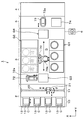
- FIG. 1 is an explanatory diagram showing an outline of the internal configuration of the substrate processing apparatus 1 according to the first embodiment.
- 2 and 3 are a front view and a rear view showing an outline of the internal configuration of the substrate processing device 1, respectively.
- the substrate processing apparatus 1 includes, for example, a cassette station 2 in which a cassette C is carried in and out of the outside, and a plurality of various processing units for performing a predetermined process such as resist coating process and PEB. It has a station 3 and.
- the substrate processing device 1 has a configuration in which the cassette station 2, the processing station 3, and the interface station 5 that transfers the wafer W between the exposure device 4 adjacent to the processing station 3 are integrally connected. ing. Further, the substrate processing device 1 has a control unit 6 that controls the substrate processing device 1.
- the cassette station 2 is divided into, for example, a cassette loading / unloading section 10 and a wafer transport section 11.
- the cassette loading / unloading section 10 is provided at the end of the substrate processing device 1 on the negative direction in the Y direction (left direction in FIG. 1).
- the cassette loading / unloading section 10 is provided with a cassette mounting table 12.
- a plurality of, for example, four mounting plates 13 are provided on the cassette mounting table 12.
- the mounting plates 13 are provided side by side in a row in the horizontal X direction (vertical direction in FIG. 1).
- the cassette C can be mounted on these mounting plates 13 when the cassette C is carried in and out of the substrate processing device 1.
- the wafer transfer unit 11 is provided with a wafer transfer unit 21 that is movable on a transfer path 20 extending in the X direction.
- the wafer transfer unit 21 is also movable in the vertical direction and around the vertical axis ( ⁇ direction), and the cassette C on each mounting plate 13 and the transfer unit of the third block G3 of the processing station 3 described later. Wafer W can be conveyed between them.
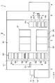
- the processing station 3 is provided with a plurality of blocks G1, G2, G3, and G4 having various units, for example, the first to fourth blocks.
- a first block G1 is provided on the front side of the processing station 3 (negative direction side in the X direction in FIG. 1), and a second block G1 is provided on the back side (positive direction side in the X direction in FIG. 1) of the processing station 3.
- Block G2 is provided.
- a third block G3 is provided on the cassette station 2 side of the processing station 3 (negative direction side in the Y direction in FIG. 1), and the interface station 5 side of the processing station 3 (positive direction side in the Y direction in FIG. 1). Is provided with a fourth block G4.
- a plurality of liquid treatment units for example, a development processing unit 30 as a development processing unit for developing the wafer W, and a resist liquid are applied to the wafer W to form a resist film.
- the resist coating units 31 to be processed are arranged in this order from the bottom.
- the development processing unit 30 and the resist coating unit 31 are arranged side by side in the horizontal direction.
- the number and arrangement of the developing processing unit 30 and the resist coating unit 31 can be arbitrarily selected.
- spin coating is performed, for example, by applying a predetermined processing liquid on the wafer W.
- the processing liquid is discharged onto the wafer W from the coating nozzle, and the wafer W is rotated to diffuse the processing liquid on the surface of the wafer W.
- the configuration of the developing processing unit 30 will be described later.
- a heat treatment unit 40 as a heat treatment unit that performs heat treatment such as heating and cooling of the wafer W and a peripheral exposure unit 41 that exposes the outer peripheral portion of the wafer W are arranged in the vertical direction. They are arranged side by side in the horizontal direction. The number and arrangement of the heat treatment unit 40 and the peripheral exposure unit 41 can also be arbitrarily selected. The configuration of the heat treatment unit 40 will be described later.
- a plurality of delivery units 50 are provided in the third block G3. Further, the fourth block G4 is provided with a plurality of delivery units 60, and a defect inspection unit 61 is provided on the plurality of delivery units 60. The configuration of the defect inspection unit 61 will be described later.
- a wafer transfer region D is formed in a region surrounded by the first block G1 to the fourth block G4.
- a wafer transfer unit 70 is arranged in the wafer transfer area D.
- the wafer transfer unit 70 has, for example, a transfer arm 70a that can move in the Y direction, the front-rear direction, the ⁇ direction, and the vertical direction.
- the wafer transfer unit 70 moves in the wafer transfer area D and transfers the wafer W to predetermined units in the surrounding first block G1, second block G2, third block G3, and fourth block G4. it can.
- a plurality of wafer transfer units 70 are arranged one above the other as shown in FIG. 3, for example, and the wafer W can be transferred to predetermined units having the same height of the blocks G1 to G4, for example.
- a shuttle transfer unit 71 that linearly conveys the wafer W between the third block G3 and the fourth block G4 is provided.
- the shuttle transport unit 71 is linearly movable in the Y direction of FIG. 3, for example.
- the shuttle transfer unit 71 moves in the Y direction while supporting the wafer W, and the wafer W is located between the transfer unit 50 of the third block G3 and the transfer unit 60 of the fourth block G4 having the same height. Can be transported.
- a wafer transfer unit 72 is provided on the X-direction positive side of the third block G3.
- the wafer transfer unit 72 has, for example, a transfer arm 72a that can move in the front-rear direction, the ⁇ direction, and the up-down direction.
- the wafer transfer unit 72 can move up and down while supporting the wafer W to transfer the wafer W to each transfer unit 50 in the third block G3.
- the interface station 5 is provided with a wafer transfer unit 73 and a transfer unit 74.
- the wafer transfer unit 73 has, for example, a transfer arm 73a that can move in the Y direction, the ⁇ direction, and the vertical direction.
- the wafer transfer unit 73 can, for example, support the wafer W on the transfer arm 73a and transfer the wafer W between each transfer unit 60, the transfer unit 74, and the exposure apparatus 4 in the fourth block G4.
- the control unit 6 described above is, for example, a computer and has a program storage unit (not shown).
- the program storage unit stores a program that controls the operation of drive systems such as the various processing units and transfer units described above, and controls the processing of the wafer W, including the processing condition adjustment processing in the substrate processing apparatus 1. ..
- the program may be recorded on a computer-readable storage medium H and may be installed on the control unit 6 from the storage medium H.
- the developing processing unit 30 has a processing container 100 whose inside can be sealed.
- a wafer W carry-in outlet (not shown) is formed on the side surface of the processing container 100 on the wafer transfer unit 70 side, and an open / close shutter (not shown) is provided at the carry-in outlet.
- a spin chuck 110 for holding and rotating the wafer W is provided in the central portion of the processing container 100.
- the spin chuck 110 has a horizontal upper surface, and for example, a suction port (not shown) for sucking the wafer W is provided on the upper surface. By suction from this suction port, the wafer W can be sucked and held on the spin chuck 110.
- a chuck drive unit 111 equipped with a motor or the like is provided below the spin chuck 110.
- the spin chuck 110 can be rotated to a predetermined speed by the chuck drive unit 111.
- the chuck drive unit 111 is provided with a lifting drive source such as a cylinder, and the spin chuck 110 can be raised and lowered.
- a cup 112 that receives and collects the liquid scattered or dropped from the wafer W is provided.
- An exhaust pipe 113 for discharging the recovered liquid and an exhaust pipe 114 for evacuating the atmosphere inside the cup 112 and exhausting the collected liquid are connected to the lower surface of the cup 112.
- a rail 120 extending along the Y direction is formed on the X-direction negative direction (downward direction in FIG. 5) side of the cup 112.
- the rail 120 is formed, for example, from the outside of the cup 112 on the negative direction in the Y direction (left direction in FIG. 5) to the outside on the positive direction in the Y direction (right direction in FIG. 5).
- An arm 121 is attached to the rail 120.
- the arm 121 supports a coating nozzle 122 that supplies a developing solution onto the wafer W.
- the arm 121 is movable on the rail 120 by the nozzle drive unit 123 shown in FIG.
- the coating nozzle 122 can move from the standby portion 124 installed on the outside of the cup 112 on the positive side in the Y direction to the upper part of the center of the wafer W in the cup 112, and further on the wafer W of the wafer W. Can move in the radial direction.
- the arm 121 can be raised and lowered by the nozzle driving unit 123, and the height of the coating nozzle 122 can be adjusted.
- a supply pipe 125 for supplying a developing solution to the coating nozzle 122 is connected to the coating nozzle 122.
- the supply pipe 125 communicates with the developer supply source 126 that stores the developer inside. Further, the supply pipe 125 is provided with a supply equipment group 127 including a valve for controlling the flow of the developing solution, a flow rate adjusting unit, and the like.
- the structure of the resist coating unit 31 is the same as the structure of the development processing unit 30 described above. However, the processing liquid supplied from the coating nozzle differs between the developing processing unit 30 and the resist coating unit 31.
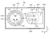
- 6 and 7 are a vertical sectional view and a horizontal sectional view showing an outline of the configuration of the heat treatment unit 40, respectively.
- the heat treatment unit 40 includes a heating unit 131 for heat-treating the wafer W and a cooling unit 132 for cooling the wafer W in the housing 130.
- a heating unit 131 for heat-treating the wafer W and a cooling unit 132 for cooling the wafer W in the housing 130.
- a cooling unit 132 for cooling the wafer W in the housing 130.
- carry-in / out outlets 133 for carrying in / out the wafer W are formed on both side surfaces in the vicinity of the cooling portion 132 of the housing 130.
- the heating unit 131 is a hot plate accommodating unit that is located on the upper side and is movable up and down, and is located on the lower side and is integrated with the lid body 140 to form a processing chamber S. It is equipped with 141.
- the lid 140 has a substantially tubular shape with an open lower surface, and covers the upper surface, which is the surface to be processed, of the wafer W placed on the hot plate 142 described later.
- An exhaust portion 140a is provided at the center of the upper surface of the lid 140.
- the atmosphere in the processing chamber S is exhausted from the exhaust unit 140a.
- the lid body 140 is provided with a temperature sensor 143 which is a temperature measuring unit for measuring the temperature of the lid body 140.
- the temperature sensor 143 is provided at the end of the lid 140, but it may be provided at the center of the lid 140 or the like.
- a wafer W is placed in the center of the hot plate accommodating portion 141, and a hot plate 142 for heating the placed wafer W is provided.
- the hot plate 142 has a thick substantially disk shape, and a heater 150 for heating the upper surface of the hot plate 142, that is, the mounting surface of the wafer W is provided inside the hot plate 142.
- the heater 150 for example, an electric heater is used. The configuration of the hot plate 142 will be described later.
- the hot plate accommodating portion 141 is provided with an elevating pin 151 that penetrates the hot plate 142 in the thickness direction.
- the elevating pin 151 can be elevated and lowered by an elevating drive unit 152 such as a cylinder, and can project to the upper surface of the hot plate 142 to transfer the wafer W to and from the cooling plate 170 described later.
- the hot plate accommodating portion 141 includes, for example, an annular holding member 160 that accommodates the hot plate 142 and holds the outer peripheral portion of the hot plate 142, and a substantially tubular support that surrounds the outer peripheral portion of the holding member 160. It has a ring 161.
- the cooling unit 132 adjacent to the heating unit 131 is provided with, for example, a cooling plate 170 on which the wafer W is placed and cooled.
- the cooling plate 170 has a substantially rectangular flat plate shape, and the end face on the heating portion 131 side is curved in an arc shape.
- a cooling member such as a Peltier element is built in the cooling plate 170, and the cooling plate 170 can be adjusted to a predetermined set temperature.
- the cooling plate 170 is supported by a support arm 171 as shown in FIG. 6, for example, and the support arm 171 is attached to a rail 172 extending in the X direction on the heating unit 131 side.
- the cooling plate 170 can be moved on the rail 172 by a drive mechanism 173 attached to the support arm 171. As a result, the cooling plate 170 can move to the upper part of the hot plate 142 on the heating unit 131 side.
- the cooling plate 170 is formed with two slits 174 along the X direction in FIG.
- the slit 174 is formed from the end surface of the cooling plate 170 on the heating portion 131 side to the vicinity of the central portion of the cooling plate 170.
- the slit 174 prevents interference between the cooling plate 170 that has moved to the heating unit 131 side and the elevating pin 151 on the hot plate 142.
- an elevating pin 175 is provided below the cooling plate 170 located in the cooling unit 132.
- the elevating pin 175 can be elevated by the elevating drive unit 176.
- the elevating pin 175 rises from below the cooling plate 170, passes through the slit 174, projects above the cooling plate 170, and is between, for example, a wafer transfer unit 70 that enters the inside of the housing 130 from the carry-in outlet 133. Wafer W can be delivered.
- FIG. 8 is a plan view showing an outline of the configuration of the hot plate 142.
- the hot plate 142 is divided into a plurality of, for example, five hot plate regions (hereinafter, may be referred to as “channels”) R1 to R5.
- the hot plate 142 is divided into, for example, a circular channel R1 located at the center when viewed from a plane, and channels R2 to R5 obtained by dividing the circumference of the channel R1 into four equal parts in an arc shape.
- a heater 180 is individually built in each channel R1 to R5 of the hot plate 142, and each channel R1 to R5 can be individually heated.
- the calorific value of the heaters 180 of each channel R1 to R5 is adjusted by, for example, the temperature control unit 181.
- the temperature control unit 181 can adjust the calorific value of each heater 180 to control the temperature of each channel R1 to R5 to a predetermined set temperature.
- the temperature setting in the temperature control unit 181 is performed by the control unit 6.
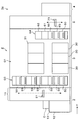
- the defect inspection unit 61 has a casing 190 as shown in FIGS. 9 and 10.
- a mounting table 200 on which the wafer W is mounted is provided in the casing 190.
- the mounting table 200 can be freely rotated and stopped by a rotation driving unit 201 such as a motor.
- a guide rail 202 extending from one end side (negative direction side in the X direction in FIG. 10) to the other end side (positive direction side in the X direction in FIG. 10) in the casing 190 is provided. ..
- the mounting table 200 and the rotary drive unit 201 are provided on the guide rail 202, and can be moved along the guide rail 202 by the drive unit 203.
- An imaging unit 210 is provided on the side surface of the casing 190 on the other end side (the positive direction side in the X direction in FIG. 10).
- a wide-angle CCD camera is used as the image pickup unit 210.
- a half mirror 211 is provided near the center of the upper part of the casing 190.
- the half mirror 211 is provided at a position facing the image pickup unit 210 in a state in which the mirror surface is inclined 45 degrees upward from the state in which the mirror surface faces vertically downward toward the image pickup section 210.
- An illumination unit 212 is provided above the half mirror 211.
- the half mirror 211 and the illumination unit 212 are fixed to the upper surface inside the casing 190.
- the illumination from the illumination unit 212 passes through the half mirror 211 and is illuminated downward. Therefore, the light reflected by the object below the illumination unit 212 is further reflected by the half mirror 211 and taken into the image pickup unit 210. That is, the imaging unit 210 can image an object in the irradiation region of the illumination unit 212.
- the wafer transfer unit 21 takes out the wafer W from the cassette C on the cassette mounting table 12 and transfers it to the transfer unit 50 of the processing station 3.
- the wafer W is transferred by the wafer transfer unit 70 to the heat treatment unit 40 of the second block G2 and subjected to temperature control processing. After that, the wafer W is conveyed to the resist coating unit 31 of the first block G1 to form a resist film on the wafer W. After that, the wafer W is transferred to the heat treatment unit 40 and pre-baked (PAB: Pre-Applied Bake). In the pre-baking treatment, the subsequent PEB treatment, and the post-baking treatment, the same heat treatment is performed. However, the heat treatment units 40 used for each heat treatment are different from each other.
- the wafer W is conveyed to the peripheral exposure unit 41 and subjected to peripheral exposure processing.
- the wafer W is conveyed to the exposure apparatus 4 and exposed in a predetermined pattern.
- the wafer W is transferred to the heat treatment unit 40 and subjected to PEB treatment. After that, the wafer W is transferred to, for example, the development processing unit 30 for development processing. After the development process is completed, the wafer W is transferred to the heat treatment unit 40 and post-baked. Then, the wafer W is conveyed to the defect inspection unit 61, and the wafer W is inspected for defects. In the defect inspection, inspections such as whether there are scratches or foreign matter adhered are performed. After that, the wafer W is conveyed to the cassette C on the cassette mounting table 12, and a series of photolithography steps is completed.
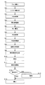
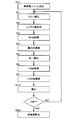
- FIG. 11 is a flowchart for explaining the adjustment process of the processing conditions of the PEB process.
- FIG. 12 is a conceptual diagram of the temperature distribution estimation method.
- the set temperature of each channel R1 to R5 of the hot plate 142 during the PEB process is adjusted.
- the adjustment process is performed, for example, when the substrate processing device 1 is introduced, when the substrate processing device 1 is maintained, and the like.
- step S1 the adjustment wafer W (hereinafter, referred to as “adjustment wafer W”) is carried in (step S1). Specifically, in the adjustment process, the operator places the cassette C containing the adjustment wafer W on the cassette mounting table 12, so that the adjustment wafer W is taken out from the cassette C and the next step is performed. Is transported to the resist coating unit.
- the adjusting wafer W is a bare wafer.
- a resist film is formed on the adjusting wafer W (step S2). Specifically, in the resist coating unit 31, a resist film is formed on the adjusting wafer W under predetermined coating treatment conditions.
- PAB processing process After that, PAB processing is performed on the adjustment wafer W (step S3). Specifically, the adjusting wafer W on which the resist film is formed is conveyed to the heat treatment unit 40 for PAB processing, and PAB processing is performed under predetermined PAB processing conditions.
- the resist film is formed and the adjusting wafer W is imaged before the uniform exposure process described later (step S4).
- the adjustment wafer W subjected to the PAB treatment is conveyed to the defect inspection unit 61, and the surface thereof is imaged by the imaging unit 210.
- the wafer W in the imaging result F1 is divided into, for example, 437 regions, and in each region, the average value of the brightness values of R (red), G (green), and B (blue) is average. Is calculated.
- a table is created in which the coordinates of the area and the average value of the brightness values of each of R, G, and B are associated with each other.
- captured images hereinafter, referred to as “pre-exposure captured images” I1 are acquired for each of R, G, and B.
- the adjustment wafer W is subjected to a uniform exposure process (step S5). Specifically, the adjustment wafer W imaged in the pre-exposure imaging step of step S4 is conveyed to the exposure apparatus 4, and a uniform exposure process is performed in which each region of the wafer surface is exposed with a constant exposure amount. In the exposure apparatus 4, during the uniform exposure process, for example, exposure is performed for each exposure region with the same exposure intensity and the same exposure time without using a reticle.
- the exposure amount of each region of the wafer surface in the uniform exposure process is less than the exposure amount at the time of actual processing, that is, at the time of mass production of the resist pattern, and specifically, it is set to 1/2 of the exposure amount at the time of actual processing. ..
- PEB processing process After the uniform exposure step, the adjustment wafer W is subjected to PEB processing (step S6). Specifically, the adjusting wafer W that has undergone uniform exposure processing is conveyed to the heat treatment unit 40 for PEB processing, which is the object for adjusting the processing conditions, and the PEB processing is performed under the currently set PEB processing conditions. It is said.
- the image of the adjusting wafer W is taken again (step S7). Specifically, the PEB-processed and undeveloped adjustment wafer W is conveyed to the defect inspection unit 61, and the surface thereof is imaged by the imaging unit 210. At this time, since it is undeveloped, what is imaged by the imaging unit 210 is not the resist pattern but the latent image formed on the resist film on the wafer W. Then, based on the imaging result F2, captured images (hereinafter, referred to as “post-PEB captured images”) I2 are acquired for each of R, G, and B.
- post-PEB captured images captured images
- the control unit 6 estimates the in-plane temperature distribution of the adjustment wafer W during the PEB process based on the imaging result in the pre-exposure imaging step and the imaging result in the PEB post-exposure imaging step (step S8). ). Specifically, the control unit 6 determines the adjustment wafer W at the time of PEB processing based on the color information of the pre-exposure image I1 acquired in the pre-exposure image capture step and the color information of the post-PEB image I2. Estimate the in-plane temperature distribution.
- the color information is luminance information of a specific wavelength (color).
- control unit 6 first receives the pre-exposure image I1 of R, G and B acquired in the pre-exposure imaging step and the post-PEB image of R, G and B acquired in the post-PEB imaging step. Shading correction Sh is performed on each of the captured image I2.
- the shading correction Sh can remove luminance unevenness caused by imaging conditions (sensitivity of the image sensor, optical system, moving speed of the mounting table 200, etc.).
- the control unit 6 determines the difference ⁇ of the brightness values between the pre-exposure image I1 ′ and the post-PEB image I2 ′ that have been shade-corrected for each R, G, and B, and for each pixel in the captured image. calculate.
- the control unit 6 is in-plane of the adjustment wafer W during PEB processing from the calibration curve Lr showing the relationship between the difference ⁇ r for R and the temperature and the difference ⁇ r for R calculated for each pixel. Obtain the temperature distribution Pr. Further, the control unit 6 is in-plane of the adjustment wafer W during PEB processing from the calibration curve Lg showing the relationship between the difference ⁇ g for G and the temperature and the difference ⁇ g for G calculated for each pixel. Obtain the temperature distribution Pg. Further, the control unit 6 uses the calibration curve Lb showing the relationship between the difference ⁇ b for B and the temperature and the difference ⁇ b for B calculated for each pixel to determine the in-plane temperature of the adjustment wafer W during PEB processing. Obtain the distribution Pb.
- the calibration curves Lr, Lg, and Lb have been obtained in advance.
- the acquisition method will be described later.
- the control unit 6 selects one of the three acquired in-plane temperature distributions Pr, Pg, and Pb of the adjustment wafer W during PEB processing.
- the in-plane temperature distribution of the adjustment wafer W during the PEB treatment which is acquired based on the captured image of the wavelength, that is, the color corresponding to the film thickness of the resist film, is selected. More specifically, when the resist film is thick, the in-plane temperature distribution Pr acquired based on the captured image of R having a long wavelength is selected, and when the resist film is thin, it is based on the captured image of B having a short wavelength.
- the acquired in-plane temperature distribution Pb is selected.
- control unit 6 estimates the in-plane temperature distribution of the adjustment wafer W during the PEB process based on the captured image of the wavelength corresponding to the film thickness of the resist film.
- the in-plane temperature distribution based on the captured image of other wavelengths is selected. Acquisition may be omitted.
- the control unit 6 determines the processing conditions for the PEB processing based on the estimation result of the in-plane temperature distribution of the adjustment wafer W during the PEB processing (step S9). Specifically, the control unit 6 determines the processing conditions for the PEB processing based on the in-plane temperature distribution of the adjusting wafer W during the PEB processing selected in the temperature distribution estimation step. For example, the control unit 6 determines the set temperature of each of the channels R1 to R5 of the hot plate 142 based on the following equation (1), and more specifically, from the reference temperature determined for each resist film type. The amount of deviation (offset amount) is determined for each channel of the hot plate 142.
- O is a matrix showing the offset amount of each channel of the hot plate 142
- T is a matrix showing the in-plane temperature distribution of the adjustment wafer W during PEB processing
- A is a transformation matrix. ..
- the resist film formed on the adjusting wafer W is removed (step S10).
- the adjusting wafer W imaged in the post-PEB imaging step is conveyed to the resist coating unit 31 as a removing unit, and the thinner liquid is adjusted from a discharge nozzle (not shown) that discharges the thinner liquid. It is supplied to W, and the resist film on the adjusting wafer W is peeled off.
- a unit for removal treatment may be provided separately from the resist coating unit 31 and the like.
- step S11 the image of the adjusting wafer W is taken again (step S11). Specifically, the adjustment wafer W from which the resist film has been removed is conveyed to the defect inspection unit 61, the surface of which is imaged by the imaging unit 210, and a substrate image showing the state of the wafer surface is acquired.
- control unit 6 determines whether or not the adjustment wafer W can be reused based on the substrate image acquired in the imaging step after removal (step S12). Specifically, the control unit 6 compares the substrate image of the adjustment wafer W acquired in the removal imaging step with the substrate image of the unprocessed bare wafer acquired in advance, and adjusts based on the comparison result. It is determined whether or not the wafer W for use is reusable.
- step S13 If it is not reusable (in the case of step S12 and NO), the control unit 6 notifies that it cannot be reused (step S13). Specifically, the control unit 6 causes, for example, display a warning to the effect that the adjustment wafer W cannot be reused on the display unit (not shown).
- the control unit 6 carries out the adjustment wafer W (step S14). Specifically, the adjusting wafer W is returned to the original cassette C on the cassette mounting table 12 by the wafer transfer unit 21. If it is not reusable, the adjusting wafer may be transported to the disposal cassette C separately placed on the cassette mounting table 12. As a result, the adjustment process of the processing conditions of the PEB process is completed. In the actual processing after the adjustment processing of the processing conditions of the PEB processing described above is completed, the PEB processing is performed under the processing conditions determined by the adjustment processing.
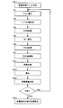
- FIG. 13 is a flowchart for explaining a method of acquiring the calibration curves Lr, Lg, and Lb.
- the one used for acquiring the calibration curve is determined according to user input or the like (step). S21).
- the calibration curve acquisition wafer W (hereinafter, referred to as “calibration curve acquisition wafer W”) is carried in in the same manner as in step S1.
- the calibration curve acquisition wafer W is a bare wafer.
- PAB processing process After that, the PAB process is performed on the calibration curve acquisition wafer W in the same manner as in step S3.
- step S5 (Uniform exposure process) Next, in the same manner as in step S5, a uniform exposure process is performed on the calibration curve acquisition wafer W.
- PEB processing process After the uniform exposure step, PEB processing is performed on the calibration curve acquisition wafer W in the same manner as in step S6.
- the PEB treatment is performed in the heat treatment unit 40 determined in step S21.
- step S7 the image of the calibration curve acquisition wafer W is performed.
- step S14 the calibration curve acquisition wafer W is carried out.
- Each step from the carry-in step of step S1 to the carry-out step of step S14 is performed on each of a plurality of (N) calibration curve acquisition wafers W.
- the temperature of the hot plate 142 in the PEB processing step is different for each wafer W for obtaining a calibration curve.
- the temperatures of the channels R1 to R5 of the hot plate 142 are the same.
- the calibration curves Lr, Lg, and Lb are calculated based on the captured images acquired in the pre-exposure imaging step and the captured images acquired in the post-PEB imaging step for the plurality of calibration curve acquisition wafers W. Will be done. Specifically, in the case of the calibration line Lr, first, the average R brightness in the wafer surface in the image captured in the pre-exposure imaging step is set to the gray value Ir1 and the gray value Ir1 and the in-wafer surface in the image captured in the post-PEB imaging step.
- the calibration curves Lg and Lb are also obtained in the same manner as the calibration curve Lr.
- the adjustment processing of the PEB processing conditions includes the pre-exposure imaging step of imaging the adjustment wafer W before the uniform exposure processing on which the resist film is formed, and the pre-exposure imaging step.
- the PEB processing step of performing PEB processing on the adjusting wafer W subjected to the uniform exposure processing the post-PEB imaging step of imaging the PEB-treated adjusting wafer W, and the imaging result in the pre-exposure imaging step.
- the PEB processing condition determination step of determining the processing condition of the PEB processing is included. Therefore, in the present embodiment, the PEB treatment is actually performed under the currently set processing conditions instead of the in-plane temperature distribution of the line width of the resist pattern, and the adjustment wafer W estimated from the imaging result after the processing.
- the processing conditions for the PEB treatment are determined based on the in-plane temperature distribution. Therefore, according to the present embodiment, the PEB treatment can be performed so that the treatment result (that is, the temperature of the wafer W) becomes uniform in the wafer surface. Therefore, it is possible to form a resist pattern having higher in-plane uniformity of line width.
- the temperature of the wafer W in the wafer surface can be made uniform at the reference temperature set for each resist film type. Therefore, it is possible to suppress variations in the temperature of the wafer W between the heat treatment units 40 for PEB processing.
- the control unit 6 obtains wavelengths corresponding to the film thickness of the resist film from the in-plane temperature distributions Pr, Pg, and Pb of the three acquired adjustment wafers W during PEB processing.
- the in-plane temperature distribution of the adjustment wafer W at the time of PEB processing acquired based on the captured image of the above is selected. That is, the control unit 6 estimates the in-plane temperature distribution of the adjustment wafer W during the PEB process based on the captured image for one wavelength according to the film thickness of the resist film. Therefore, the in-plane temperature distribution during the PEB treatment can be estimated more accurately, and the PEB treatment result can be made more uniform in the wafer plane.
- control unit 6 selects one of the three in-plane temperature distributions Pr, Pg, and Pb of the adjustment wafer W during PEB processing, the following may be performed.
- a temperature sensor is provided for the hot plate 142, and an in-plane temperature distribution in which the measurement result of the temperature sensor and the estimated temperature of the pixels corresponding to the arrangement position of the temperature sensor are closest to each other is selected. You may do so.
- control unit 6 estimates the in-plane temperature distribution of the adjustment wafer W during one PEB process based on all the captured images of R, G, and B by using the following equation (2). It may be.
- control unit 6 may use the following equation (3) to estimate the in-plane temperature distribution of the adjustment wafer W during PEB processing.
- the exposure amount of each region of the wafer surface in the uniform exposure process is less than the exposure amount in the actual process, for example, halved. Therefore, when the PEB treatment is performed during the adjustment processing of the processing conditions of the PEB treatment, the amount of change in the film thickness of the resist film before and after the PEB treatment becomes large due to the difference in the PEB treatment result. As a result, the amount of change in brightness in the captured image before and after the PEB processing becomes large due to the difference in the PEB processing result. That is, even if the difference in the PEB processing result is slight, the difference in brightness between the pre-exposure image and the post-PEB image is large.
- the in-plane temperature distribution of the adjustment wafer W during the PEB process can be estimated with high accuracy based on the pre-exposure image and the post-PEB image. It should be noted that 1/2 of the exposure amount during the actual processing corresponds to the exposure amount applied to the edge portion of the resist pattern.
- the adjustment wafer W from which the resist film has been removed can be reused based on the substrate image acquired in the imaging step after removal. Therefore, the consumption of the adjustment wafer W can be suppressed without impairing the adjustment accuracy of the processing conditions.
- a bare wafer is used as the adjustment wafer W. Therefore, the processing conditions for the PEB processing can be appropriately determined.
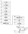
- FIG. 14 is a flowchart for explaining the processing for adjusting the processing conditions according to the second embodiment.
- the processing conditions for the PEB treatment are adjusted, whereas in the present embodiment, the processing conditions for the development processing are adjusted.
- the processing conditions for the development process are adjusted, for example, after the adjustment of the processing conditions for the PEB process. Since the adjustment of the processing conditions for the PEB processing is performed when the substrate processing apparatus 1 is introduced as described above, the processing conditions for the development processing are also adjusted at the same timing. However, it is possible to adjust the processing conditions of the developing process without adjusting the processing conditions of the PEB processing.
- step S1 In the process of adjusting the processing conditions of the developing process, first, the adjusting wafer W is carried in as in step S1 described above.
- PAB processing process After that, the PAB process is performed on the adjustment wafer W in the same manner as in step S3 described above (step S3).
- step S5 (Uniform exposure process)
- the adjustment wafer W is subjected to a uniform exposure process. Even in the adjustment process of the processing conditions of the development process, the exposure amount of each region of the wafer surface in the uniform exposure process is less than the exposure amount in the actual process, for example, halved.
- PEB processing process After the uniform exposure step, PEB processing is performed on the adjusting wafer W in the same manner as in step S6 described above. However, if the processing conditions for the PEB treatment have been adjusted, the PEB treatment is performed under the adjusted PEB processing conditions.
- the adjustment wafer W is subjected to a developing process (step S31). Specifically, the adjustment wafer W subjected to the PEB treatment is conveyed to the development processing unit 30 whose processing conditions are to be adjusted, and the development processing is performed under the currently set development processing conditions.
- step S32 the image of the adjusting wafer W is taken again (step S32). Specifically, the adjustment wafer W that has undergone development processing is conveyed to the defect inspection unit 61, and the surface thereof is imaged by the image pickup unit 210, and the image image (hereinafter referred to as “development image image”) I3. Is obtained.
- the control unit 6 has a film thickness of the resist film after the development process on the adjusting wafer W based on the imaging result in the post-development imaging step (hereinafter, referred to as “resist film residual film thickness”).
- the in-plane distribution of is estimated (step S33). Specifically, the control unit 6 calculates or estimates the in-plane distribution of the residual film thickness of the resist film of the adjusting wafer W based on the color information of the developed image I3 for B (blue). More specifically, the control unit 6 calculates the residual film thickness of the resist film based on the brightness and the calibration curve Ldev acquired in advance for each pixel in the developed image I3 after development for B.
- the in-plane distribution of the residual film thickness is acquired.
- the calibration curve Ldev shows the relationship between the brightness of the developed image I3 for B and the residual film thickness of the resist film. The method of acquiring the calibration curve Ldev will be described later.
- the in-plane distribution of the remaining film thickness amount was calculated based on the captured image of B, but the in-plane distribution of the remaining film thickness amount was calculated based on the captured image of G and the captured image of R.
- the distribution may be calculated.
- the estimation may be performed based on the captured image of the wavelength corresponding to the film thickness of the resist film.
- the control unit 6 determines the processing conditions for the development process based on the estimation result of the in-plane distribution of the residual film thickness of the resist film (step S34). Specifically, the control unit 6 determines and corrects the supply time of the developer as a processing condition for the developing process, for example, based on the in-plane distribution of the residual film thickness of the resist film on the adjusting wafer W. .. More specifically, in the adjustment wafer W, when the residual film thickness of the resist film is close to the target amount at the center of the wafer and is appropriate and larger than the target amount at the outer periphery of the wafer, the control unit 6 moves to the outer periphery of the wafer.
- the processing conditions of the developing process are determined so that the supply of the developing solution is added.
- the length ⁇ t of the additional supply time of the developer to the outer peripheral portion of the wafer is calculated from, for example, the correction curve Lamd showing the relationship between the supply time of the developer and the amount of the remaining film thickness.
- the correction curve Lamd has been acquired in advance. The acquisition method will be described later.
- the calculated length ⁇ t of the additional supply time of the developer to the outer peripheral portion of the wafer that is, the determined processing conditions for the developing process are stored in the storage unit (not shown), and during the subsequent actual processing, etc. It is used in the development process in.
- steps S10 to S14 described above are performed, whereby the adjustment process of the processing conditions of the development process is completed.
- FIG. 15 is a flowchart for explaining a method of acquiring the calibration curve Ldev and the correction curve Lamd.
- step S41 When acquiring the calibration curve Ldev, first, among the plurality of development processing units 30, the one used for acquiring the calibration curve and the correction curve is determined according to user input or the like (step S41).
- the wafer W for acquiring the calibration curve and the correction curve (hereinafter, referred to as “the wafer W for acquiring the calibration curve”) is carried in in the same manner as in step S1.
- the calibration curve acquisition wafer W is also a bare wafer.
- PAB processing process After that, the PAB process is performed on the calibration curve acquisition wafer W in the same manner as in step S3.
- step S5 (Uniform exposure process) Next, in the same manner as in step S5, a uniform exposure process is performed on the calibration curve acquisition wafer W.
- PEB processing process After the uniform exposure step, PEB processing is performed on the calibration curve acquisition wafer W in the same manner as in step S6.
- step S31 the development process is performed on the calibration curve acquisition wafer W in the same manner as in step S31.
- the developing process is performed in the developing process unit 30 determined in step S41, and the developing solution is supplied only to the central portion of the wafer from the coating nozzle 122 during spin coating of the developing solution.
- step S32 the image of the calibration curve acquisition wafer W is performed. As a result, the captured image for at least B is acquired.
- step S14 the calibration curve acquisition wafer W is carried out.
- the residual film thickness of the resist film of the calibration curve acquisition wafer W is acquired (step S42). Specifically, for example, the calibration curve acquisition wafer W that has been subjected to PEB treatment is conveyed to an external film thickness measuring device (not shown), and the amount of residual film thickness of the resist film in the center of the wafer is measured. To. The residual film thickness amount may be measured by providing a film thickness measuring device in the substrate processing device 1 and using the film thickness measuring device.
- the calibration curve Lpeb and the correction curve Lamd are calculated based on the captured images of the calibration curve acquisition wafer W acquired in the post-development imaging step for the plurality of calibration curve acquisition wafers W (step S43). ..
- the explanatory variable is the B brightness in the tag number in the imaging step after development
- the objective variable is the residual film amount of the resist film acquired in the residual film amount measurement step. An approximate curve of the remaining film thickness amount with respect to the B brightness value change amount is acquired, and this is used as the calibration curve Lpeb.
- the explanatory variable is the supply time of the developer in the developing step
- the objective variable is the residual film amount of the resist film acquired in the residual film amount measuring step, and the resist with respect to the supply time of the developing solution is used.
- An approximate curve of the amount of residual film thickness of the film is acquired, and this is referred to as a correction curve Lamd.
- the development process is actually performed under the currently set processing conditions, and the development is performed based on the in-plane distribution of the film thickness of the resist film after the development process estimated from the processing result.
- the processing conditions for processing are determined. Therefore, according to the present embodiment, the development process can be performed so that the process result is uniform on the wafer surface. Therefore, it is possible to form a resist pattern having higher in-plane uniformity of line width.
- the exposure amount of each region of the wafer surface in the uniform exposure process is less than the exposure amount in the actual process, for example, halved. Therefore, when the development process is performed during the process of adjusting the processing conditions of the development process, the film thickness of the resist film after the development process is significantly different due to the difference in the development process results. As a result, the brightness of the captured image after the development process is significantly different due to the difference in the development process result. That is, even if the difference in the development processing results is slight, the brightness in the developed image will be significantly different. Therefore, the in-plane distribution of the film thickness of the resist film after the development process can be estimated with high accuracy based on the image taken after the development.
- FIG. 16 is a front view showing an outline of the internal configuration of the substrate processing apparatus 1a according to the third embodiment.
- the uniform exposure process is performed by an external exposure device 4 adjacent to the substrate processing device 1 and performing exposure during the actual process.
- the substrate processing device 1a has an exposure unit 62 independent of the exposure device 4. Then, the exposure unit 62 performs a uniform exposure process on the adjusting wafer W. With this configuration, the processing for adjusting the processing conditions can be completed in the substrate processing device 1 without using an external exposure device.
- the exposure unit 62 is provided on, for example, the defect inspection unit 61 in the fourth block G4.
- FIG. 17 is a vertical cross-sectional view showing an outline of the configuration of the heat treatment unit 40a included in the substrate processing apparatus according to the fourth embodiment.
- the lid 140 is provided with a heater 140b as a temperature control mechanism for adjusting the temperature of the lid 140.
- the conditions of the hot plate 142 at the time of PEB processing in the actual processing such as the offset amount of each channel of the hot plate 142 are adjusted, but only adjusting the conditions of the hot plate 142 is described above.
- the wafer temperature during the PEB treatment may be lower or higher than the desired temperature as a whole.
- the heater 140b that adjusts the temperature of the lid 140 as in the present embodiment, the temperature of the wafer W during the PEB treatment during the actual treatment can be set to a desired temperature. This is because the wafer W is affected by the radiant heat of the lid 140.
- the temperature of the lid 140 during the PEB treatment may differ between the adjustment treatment of the hot plate conditions during the PEB treatment and the actual treatment. is there.
- the temperature of the lid 140 during the PEB treatment can be made the same between the adjustment treatment and the actual treatment. Since the wafer W is affected by the radiant heat of the lid 140 as described above, the temperature of the lid 140 during the PEB treatment differs between the adjustment treatment and the actual treatment in the same case after the adjustment. It is possible to improve the in-plane uniformity of the PEB processing result during the actual processing.
- each of the hot plates 142 determined by the adjustment processing that is, based on the processing conditions determined by the adjustment processing.
- PEB processing is performed based on the offset amount of the channel.
- the offset amount determined by the adjustment treatment is corrected and used based on the temperature measurement result of the lid 140 of the heat treatment unit 40 by the temperature sensor 143. This is because the wafer W is affected by the radiant heat of the lid 140 as described above.
- the adjustment processing of the processing conditions of the PEB processing is performed when the substrate processing apparatus 1 is introduced or when the substrate processing apparatus 1 is maintained.
- the execution timing of the adjustment processing of the processing conditions of the PEB processing is not limited to the above.
- the control unit 6 may measure the film thickness of the resist film formed during the actual treatment, and start the adjustment processing of the processing conditions of the PEB treatment based on the measurement result. Specifically, when the measured variation in the film thickness of the resist film in the wafer surface or the average value of the film thickness in the wafer surface exceeds the threshold value, the processing conditions of the PEB process are adjusted. You may want to start.
- the film thickness of the resist film can be measured as follows.
- the wafer W on which the resist film is formed after the PEB treatment in the actual treatment is imaged by the imaging unit 210 of the defect inspection unit 61, and the film of the resist film is based on the image captured from the imaged result. Thickness can be measured / estimated.
- the execution timing of the adjustment processing of the processing conditions of the PEB processing and the developing processing may be as follows. That is, for example, the control unit 6 may estimate the line width of the resist pattern formed during the actual processing, and start the adjustment processing of the processing conditions of the PEB processing and the developing processing based on the estimation result. .. Specifically, the processing condition adjustment process may be started when the estimated variation in the line width in the wafer plane or the average value of the line width in the wafer plane exceeds the threshold value. ..
- the line width of the resist pattern can be estimated as follows.
- the wafer W on which the resist pattern is formed after the development process in the actual processing is imaged by the imaging unit 210 of the defect inspection unit 61, and the resist pattern line is based on the image captured from the imaged image.
- the width can be estimated. Further, when adjusting the processing conditions, the adjusting wafer W was placed on the cassette mounting table 12 in a state where the operator stored it in the cassette C, but it was stored in the container in the substrate processing device 1. May be good.
- FIG. 18 is a front view showing an outline of the internal configuration of the substrate processing apparatus 1b according to the fifth embodiment.
- the substrate processing apparatus 1b has an inspection unit 63.
- the defect inspection unit 61 images the entire surface of the wafer W for inspection, whereas the inspection unit 63 images only the peripheral edge of the wafer W for inspection.
- the control unit 6 executes the adjustment processing of the processing conditions of the peripheral exposure processing by the peripheral exposure unit 41. Further, the execution timing of the adjustment processing of the processing conditions of the peripheral exposure processing is determined as follows.
- the peripheral portion of the wafer W is imaged by the imaging unit (not shown) of the inspection unit 63, and the adjustment processing of the processing conditions of the peripheral exposure processing is started based on the imaging result.
- the peripheral exposure width by the peripheral exposure processing is estimated based on the imaging result, and when the estimated peripheral exposure width is abnormal, the processing condition adjustment processing of the peripheral exposure processing is started.
- the processing condition adjustment process that starts based on the imaging result of the peripheral portion of the wafer W is not limited to the processing condition adjustment process of the peripheral exposure process, but is the adjustment process of the processing conditions of other processes for the peripheral edge portion of the wafer. You may.
- EBR treatment a treatment for removing the film on the outer peripheral edge of the wafer W
- edge coating treatment a treatment for covering only the peripheral edge of the wafer W.
- a substrate processing device that processes a substrate.
- a heat treatment section that heat-treats the substrate,
- An imaging unit that images the substrate and Has a control unit
- the control unit is configured to execute an adjustment process for adjusting the processing conditions for the substrate.
- the adjustment process A pre-exposure imaging step that controls the imaging unit so that an unexposed adjustment substrate on which a resist film is formed is imaged.
- a heat treatment step of controlling the heat treatment section so that the heat treatment is performed on the adjustment substrate that has been subjected to a uniform exposure process that exposes each region of the substrate surface with a constant exposure amount.
- a temperature distribution estimation step for estimating the in-plane temperature distribution of the adjustment substrate during the heat treatment based on the imaging result in the pre-exposure imaging step and the imaging result in the post-heating imaging step.
- a substrate processing apparatus including a heat treatment condition determining step of determining the heat treatment processing conditions based on the estimation result of the in-plane temperature distribution of the adjusting substrate. According to the above (1), the heat treatment is actually performed, and the heat treatment treatment conditions are determined based on the in-plane temperature distribution of the adjustment substrate estimated from the imaging result after the heat treatment. Therefore, according to the present embodiment, the heat treatment can be performed so that the treatment result (that is, the temperature of the substrate) becomes uniform in the surface of the substrate. Therefore, it is possible to form a resist pattern having higher in-plane uniformity of line width.
- the substrate processing apparatus which has an exposure unit that performs the uniform exposure process, which is different from an external exposure apparatus that performs the exposure process during the actual process. According to the above (2), the processing for adjusting the processing conditions can be completed in the substrate processing apparatus without using an external exposure apparatus.
- the in-plane temperature distribution of the adjustment substrate during the heat treatment is estimated based on the captured image of the wavelength according to the film thickness of the resist film, the above (1) to (1).
- the substrate processing apparatus according to any one of 4). According to the above (5), the in-plane temperature distribution during the heat treatment can be estimated more accurately, and the heat treatment result can be made more uniform in the substrate surface.
- the adjustment process After the post-heating imaging step, a development processing step of controlling the development processing unit so that the development processing is performed on the adjustment substrate, and After the development processing step, a post-development imaging step of controlling the imaging unit so that the adjustment substrate is imaged, A film thickness distribution estimation step for estimating the in-plane distribution of the film thickness of the resist film after the development process and an estimation of the in-plane distribution of the film thickness on the adjustment substrate based on the imaging results in the heat treatment step.
- the substrate processing apparatus according to any one of (1) to (5) above, which includes a development processing condition determining step of determining the processing conditions of the developing process based on the result. According to the above (6), the developing process can be performed so that the processing result is uniform on the substrate surface. Therefore, it is possible to form a resist pattern having higher in-plane uniformity of line width.
- the substrate has a removing portion for removing the resist film.
- the adjustment process A removal step of controlling the removing portion so that the resist film formed on the adjusting substrate is removed.
- a post-removal imaging step that controls the imaging unit so that the adjustment substrate is imaged.
- the control unit The substrate treatment according to any one of (1) to (7) above, which is configured to start the adjustment treatment based on the estimation result of the line width of the resist pattern formed on the substrate during the actual treatment. apparatus.
- control unit Any one of (1) to (8) above, which is configured to start the adjustment processing of the processing conditions for the peripheral portion of the substrate based on the imaging result of the peripheral portion of the substrate during the actual processing.
- the substrate processing apparatus according to.
- the heat treatment section is The hot plate on which the board is placed and A lid covering the substrate on the hot plate and The substrate processing apparatus according to any one of (1) to (9) above, which has a temperature adjusting mechanism for adjusting the temperature of the lid.
- a processing condition adjusting method for adjusting processing conditions for a substrate A pre-exposure imaging step of imaging an unexposed adjustment substrate on which a resist film is formed, and After the pre-exposure imaging step, a uniform exposure step of performing a uniform exposure process of exposing each region of the substrate surface with a constant exposure amount on the adjustment substrate, and a uniform exposure step. After the uniform exposure step, a heat treatment step of performing a heat treatment on the adjustment substrate and a heat treatment step After the heat treatment step, a post-heating imaging step of imaging the adjustment substrate, and A temperature distribution estimation step for estimating the in-plane temperature distribution of the adjustment substrate during the heat treatment based on the imaging result in the pre-exposure imaging step and the imaging result in the post-heating imaging step.
- a processing condition adjusting method including a heat treatment condition determining step of determining a processing condition at the time of heat treatment based on an estimation result of an in-plane temperature distribution of the adjusting substrate.
Landscapes
- Engineering & Computer Science (AREA)
- Physics & Mathematics (AREA)
- General Physics & Mathematics (AREA)
- Manufacturing & Machinery (AREA)
- Computer Hardware Design (AREA)
- Microelectronics & Electronic Packaging (AREA)
- Power Engineering (AREA)
- Condensed Matter Physics & Semiconductors (AREA)
- Health & Medical Sciences (AREA)
- Toxicology (AREA)
- Life Sciences & Earth Sciences (AREA)
- Environmental & Geological Engineering (AREA)
- Epidemiology (AREA)
- Atmospheric Sciences (AREA)
- Public Health (AREA)
- Exposure Of Semiconductors, Excluding Electron Or Ion Beam Exposure (AREA)
Abstract
Description
各加熱領域の温度の設定では、従来、実際に、テストウェハに一連のレジストパターン形成処理を行い、レジストパターンの線幅を領域毎に測定し、該測定結果に基づいて、各加熱領域の温度を設定していた。しかし、この方法では、レジストパターンの線幅のウェハ面内での均一性は改善されるものの、ウェハの加熱処理の処理結果を、すなわちウェハの温度を、ウェハ面内で均一にすることができない。レジストパターンの線幅には、パターン露光の処理条件や現像の処理条件等も影響するからである。熱処理装置の各加熱領域の温度の設定に、実際に形成し測定したレジストパターンの線幅を用いるのではなく、特許文献1のように、レジストパターンの推定線幅を用いる場合も同様である。
レジストパターンの線幅の面内での均一性をさらに改善するためには、ウェハの加熱処理を含むレジストパターン形成のための処理それぞれを、その処理結果が基板面内で均一になるように行うことが肝要である。
図1は、第1実施形態にかかる基板処理装置1の内部構成の概略を示す説明図である。図2及び図3は、各々基板処理装置1の内部構成の概略を示す、正面図と背面図である。
現像処理ユニット30は、図4及び図5に示すように、内部を密閉可能な処理容器100を有している。処理容器100のウェハ搬送ユニット70側の側面には、ウェハWの搬入出口(図示せず)が形成され、当該搬入出口には開閉シャッタ(図示せず)が設けられている。
例えば熱処理ユニット40は、図6及び図7に示すように筐体130内に、ウェハWを加熱処理する加熱部131と、ウェハWを冷却処理する冷却部132を備えている。図7に示すように筐体130の冷却部132近傍の両側面には、ウェハWを搬入出するための搬入出口133が形成されている。
また、蓋体140には、該蓋体140の温度を測定する温度測定部である温度センサ143が設けられている。図の例では、温度センサ143は蓋体140の端部に設けられているが、蓋体140の中央部等に設けてもよい。
次にウェハWは、露光装置4に搬送され、所定のパターンで露光処理される。
PEB処理の処理条件の調整処理では、図11に示すように、まず、調整用のウェハW(以下、「調整用ウェハW」という。)が搬入される(ステップS1)。具体的には、当該調整処理に際し、作業者により、調整用ウェハWが収容されたカセットCがカセット載置台12に載置されるため、当該カセットCから調整用ウェハWが取り出され、次工程のためにレジスト塗布ユニットに搬送される。なお、調整用ウェハWは、ベアウェハである。
次いで、調整用ウェハW上にレジスト膜が形成される(ステップS2)。具体的には、レジスト塗布ユニット31において、予め定められた塗布処理条件で、調整用ウェハW上にレジスト膜が形成される。
その後、調整用ウェハWに対し、PAB処理が行われる(ステップS3)。具体的には、レジスト膜が形成された調整用ウェハWが、PAB処理用の熱処理ユニット40に搬送され、予め定められたPAB処理条件で、PAB処理が行われる。
次いで、レジスト膜が形成され、且つ、後述の均一露光処理前の、調整用ウェハWの撮像が行われる(ステップS4)。具体的には、PAB処理が行われた調整用ウェハWが、欠陥検査ユニット61に搬送され、その表面が撮像部210により撮像される。そして、図12に示すように、撮像結果F1におけるウェハWが例えば437個の領域に分割され、各領域において、R(赤)、G(緑)、B(青)それぞれの輝度値の平均値が算出される。そして、領域(ピクセル)それぞれについて、当該領域の座標と、R、G、Bそれぞれの輝度値の平均値とを対応付けたテーブルが作成される。そして、作成されたテーブルに基づいてR、G、Bそれぞれについて撮像画像(以下、「露光前撮像画像」という。)I1が取得される。
撮像画像の取得後、調整用ウェハWに対し、均一露光処理が行われる(ステップS5)。具体的には、ステップS4の露光前撮像工程で撮像された調整用ウェハWが、露光装置4に搬送され、ウェハ表面の各領域を一定の露光量で露光する均一露光処理が行われる。露光装置4では、均一露光処理の際、例えば、露光領域毎に、レチクルを用いずに、同じ露光強度且つ同じ露光時間で、露光が行われる。また、均一露光処理におけるウェハ表面の各領域の露光量は、実処理時すなわちレジストパターンの量産時の露光量未満であり、具体的には、実処理時の露光量の1/2とされる。
均一露光工程後、調整用ウェハWに対し、PEB処理が行われる(ステップS6)。具体的には、均一露光処理が行われた調整用ウェハWが、処理条件の調整対象の、PEB処理用の熱処理ユニット40に搬送され、現在設定されているPEB処理条件で、PEB処理が行われる。
次いで、調整用ウェハWの撮像が再度行われる(ステップS7)。具体的には、PEB処理が行われ未現像の調整用ウェハWが、欠陥検査ユニット61に搬送され、その表面が撮像部210により撮像される。このとき、未現像であるため、撮像部210により撮像されるのは、レジストパターンではなくウェハW上のレジスト膜に形成された潜像である。そして、撮像結果F2に基づいて、R、G、Bそれぞれについて撮像画像(以下、「PEB後撮像画像」という。)I2が取得される。
次に、制御部6は、露光前撮像工程での撮像結果と、PEB後撮像工程での撮像結果とに基づいて、PEB処理時の調整用ウェハWの面内温度分布を推定する(ステップS8)。具体的には、制御部6は、露光前撮像工程で取得された露光前撮像画像I1の色情報と、PEB後撮像画像I2の色情報とに基づいて、PEB処理時の調整用ウェハWの面内温度分布を推定する。なお、色情報とは、特定の波長(色)の輝度情報である。
より具体的には、制御部6は、まず、露光前撮像工程で取得されたR、G及びBの露光前撮像画像I1と、PEB後撮像工程で取得されたR、G及びBのPEB後撮像画像I2と、に対し、それぞれシェーディング補正Shを行う。シェーディング補正Shにより、撮像条件(撮像素子の感度、光学系、載置台200の移動速度等)に起因する輝度ムラを除去することができる。
続いて、制御部6は、R、G及びB毎、且つ、撮像画像におけるピクセル毎に、シェーディング補正された露光前撮像画像I1´とPEB後撮像画像I2´とで、輝度値の差分Δを算出する。
そして、制御部6は、Rについての上記差分Δrと温度との関係を示す検量線Lrと、ピクセル毎に算出されたRについての上記差分Δrから、PEB処理時の調整用ウェハWの面内温度分布Prを取得する。
また、制御部6は、Gについての上記差分Δgと温度との関係を示す検量線Lgと、ピクセル毎に算出されたGについての上記差分Δgから、PEB処理時の調整用ウェハWの面内温度分布Pgを取得する。
さらに制御部6は、Bについての上記差分Δbと温度との関係を示す検量線Lbと、ピクセル毎に算出されたBについての上記差分Δbから、PEB処理時の調整用ウェハWの面内温度分布Pbを取得する。
なお、上記検量線Lr、Lg、Lbは予め取得されている。その取得方法については後述する。
また、制御部6は、取得された3つのPEB処理時の調整用ウェハWの面内温度分布Pr、Pg、Pbから1つ選択する。例えば、レジスト膜の膜厚に応じた波長すなわち色についての撮像画像に基づいて取得された、PEB処理時の調整用ウェハWの面内温度分布が選択される。より具体的には、レジスト膜が厚いときは波長が長いRの撮像画像に基づいて取得された面内温度分布Prが選択され、レジスト膜が薄いときは波長が短いBの撮像画像に基づいて取得された面内温度分布Pbが選択される。つまり、制御部6は、レジスト膜の膜厚に応じた波長についての撮像画像に基づいて、PEB処理時の調整用ウェハWの面内温度分布を推定する。なお、上述のようにレジスト膜の膜厚に応じた波長についての撮像画像に基づいて取得された、上記面内温度分布を選択する場合、他の波長についての撮像画像に基づく面内温度分布の取得は省略してもよい。
温度分布推定工程後、制御部6は、PEB処理時の調整用ウェハWの面内温度分布の推定結果に基づいて、PEB処理の処理条件を決定する(ステップS9)。
具体的には、制御部6は、温度分布推定工程において選択された、PEB処理時の調整用ウェハWの面内温度分布に基づいて、PEB処理の処理条件を決定する。例えば、制御部6は、以下の式(1)に基づいて、熱板142のチャンネルR1~R5それぞれの設定温度を決定し、より具体的には、レジスト膜種毎に定められた基準温度からのずれ量(オフセット量)を熱板142のチャンネル毎に決定する。

上述の式(1)等を用いることにより、調整用ウェハWにおいて、推定されたPEB処理時の温度が基準温度より低い領域に対応するチャネルはオフセット量が増加するように、且つ、推定されたPEB処理時の温度が基準温度より高い領域に対応するオフセット量が低下するように、PEB処理の処理条件は決定される。
決定された、PEB処理の処理条件は、記憶部(図示せず)に記憶され、その後の実処理時等におけるPEB処理で用いられる。
また、調整用ウェハWに形成されたレジスト膜の除去処理が行われる(ステップS10)。具体的には、PEB後撮像工程で撮像された調整用ウェハWが、除去部としてのレジスト塗布ユニット31に搬送され、シンナー液を吐出する吐出ノズル(図示せず)からシンナー液を調整用ウェハWに供給し、当該調整用ウェハW上のレジスト膜が剥離される。なお、除去処理用のユニットをレジスト塗布ユニット31等とは別に設けてもよい。
次いで、調整用ウェハWの撮像が再度行われる(ステップS11)。具体的には、レジスト膜が除去された調整用ウェハWが、欠陥検査ユニット61に搬送され、その表面が撮像部210により撮像され、ウェハ表面の状態を示す基板画像が取得される。
次に、制御部6は、除去後撮像工程で取得された基板画像に基づいて、調整用ウェハWが再利用可能であるか否か判定する(ステップS12)。具体的には、制御部6は、除去撮像工程で取得された調整用ウェハWの基板画像と、予め取得された未処理状態のベアウェハの基板画像とを比較し、比較結果に基づいて、調整用ウェハWが再利用可能であるか否か判定する。
再利用可能でない場合(ステップS12、NOの場合)、制御部6は、再利用不可である旨の報知を行わせる(ステップS13)。具体的には、制御部6は、例えば、調整用ウェハWが再利用不可である旨の警告を表示部(図示せず)に表示させる。
再利用可能である場合(ステップS12、YESの場合)、または、ステップS11の報知工程後、制御部6は、調整用ウェハWを搬出させる(ステップS14)。具体的には、調整用ウェハWが、ウェハ搬送ユニット21によって、カセット載置台12上の元のカセットCへ戻される。なお、再利用可能でない場合は、別途カセット載置台12上に載置された廃棄用のカセットCに調整用ウェハが搬送されるようにしてもよい。
これにより、PEB処理の処理条件の調整処理は完了する。
上述のPEB処理の処理条件の調整処理が完了した後の実処理では、当該調整処理により決定された処理条件でPEB処理が行われる。
次いで、検量線取得用のウェハW(以下、「検量線取得用ウェハW」という。)が、ステップS1と同様に搬入される。なお、検量線取得用ウェハWは、ベアウェハである。
次いで、ステップS2と同様に、検量線取得用ウェハW上にレジスト膜が形成される。
その後、ステップS3と同様に、検量線取得用ウェハWに対し、PAB処理が行われる。
次いで、ステップS4と同様に、検量線取得用ウェハWの撮像が行われる。
次いで、ステップS5と同様に、検量線取得用ウェハWに対し、均一露光処理が行われる。
均一露光工程後、ステップS6と同様に、検量線取得用ウェハWに対し、PEB処理が行われる。なお、PEB処理はステップS21で決定された熱処理ユニット40で行われる。
次いで、ステップS7と同様に、検量線取得用ウェハWの撮像が行われる。
そして、ステップS14と同様に、検量線取得用ウェハWが搬出される。
そして、複数枚の検量線取得用ウェハWについての、露光前撮像工程で取得された撮像画像と、PEB後撮像工程で取得された撮像画像とに基づいて、検量線Lr、Lg、Lbが算出される。具体的には、検量線Lrの場合、まず、露光前撮像工程での撮像画像におけるウェハ面内での平均のR輝度をグレー値Ir1と、PEB後撮像工程の撮像画像におけるウェハ面内での平均のR輝度をグレー値Ir2とし、PEB処理工程での熱板142の温度毎に、グレー値変化量ΔIr(=Ir2-Ir1)が算出される。そして、説明変数をグレー値変化量、目的変数をPEB処理工程での熱板142の温度として、グレー値変化量に対する上記熱板142の温度の近似曲線が取得され、これが検量線Lrとされる。
検量線Lg、Lbの場合も検量線Lrと同様に取得される。


図14は、第2実施形態にかかる処理条件の調整処理を説明するためのフローチャートである。
第1実施形態では、PEB処理の処理条件を調整したのに対し、本実施形態では、現像処理の処理条件を調整する。現像処理の処理条件の調整処理は、例えば、PEB処理の処理条件の調整後に続いて行われる。なお、PEB処理の処理条件の調整が前述のように基板処理装置1を導入する際等に行われるため、現像処理の処理条件の調整処理も、同タイミングで行われることとなる。ただし、PEB処理の処理条件の調整を行わずに、現像処理の処理条件の調整処理を行うことは可能ではある。
現像処理の処理条件の調整処理では、まず、前述のステップS1と同様に、調整用ウェハWが搬入される。
次いで、前述のステップS2と同様に、調整用ウェハW上にレジスト膜が形成される。
その後、前述のステップS3と同様に、調整用ウェハWに対し、PAB処理が行われる(ステップS3)。
次いで、前述のステップS5と同様に、調整用ウェハWに対し、均一露光処理が行われる。現像処理の処理条件の調整処理でも、均一露光処理における、ウェハ表面の各領域の露光量は、実処理時の露光量未満で、例えば1/2とされる。
均一露光工程後、前述のステップS6と同様に、調整用ウェハWに対し、PEB処理が行われる。ただし、PEB処理の処理条件の調整後であれば、調整後のPEB処理条件でPEB処理が行われる。
その後、調整用ウェハWに対し、現像処理が行われる(ステップS31)。具体的には、PEB処理が行われた調整用ウェハWが、処理条件の調整対象の、現像処理ユニット30に搬送され、現在設定されている現像処理条件で、現像処理が行われる。
次いで、調整用ウェハWの撮像が再度行われる(ステップS32)。具体的には、現像処理が行われた調整用ウェハWが、欠陥検査ユニット61に搬送され、その表面が撮像部210により撮像され、撮像画像(以下、「現像後撮像画像」という。)I3が取得される。
次に、制御部6は、現像後撮像工程での撮像結果に基づいて、調整用ウェハWにおける、現像処理後のレジスト膜の膜厚(以下、「レジスト膜の残膜厚量」という。)の面内分布を推定する(ステップS33)。
具体的には、制御部6は、B(青)についての現像後撮像画像I3の色情報に基づいて、調整用ウェハWのレジスト膜の残膜厚量の面内分布を算出すなわち推定する。
より具体的には、制御部6は、Bについての現像後撮像画像I3におけるピクセル毎に、輝度と、予め取得された検量線Ldevとに基づいて、レジスト膜の残膜厚量を算出し、上記残膜厚量の面内分布を取得する。
なお、検量線Ldevは、Bについての現像後撮像画像I3における輝度とレジスト膜の残膜厚量との関係を示すものである。検量線Ldevの取得方法については後述する。
ここでは、Bについての撮像画像に基づいて上記残膜厚量の面内分布を算出していたが、Gについての撮像画像や、Rについての撮像画像に基づいて上記残膜厚量の面内分布を算出してもよい。また、PEB処理時の調整用ウェハWの面内温度分布の推定と同様、レジスト膜の膜厚に応じた波長についての撮像画像に基づいて推定するようにしてもよい。
残膜厚量分布推定工程後、制御部6は、レジスト膜の残膜厚量の面内分布の推定結果に基づいて、現像処理の処理条件を決定する(ステップS34)。
具体的には、制御部6は、例えば、調整用ウェハW上のレジスト膜の残膜厚量の面内分布に基づいて、現像処理の処理条件としての現像液の供給時間を決定し補正する。
より具体的には、制御部6は、調整用ウェハWにおいて、レジスト膜の残膜厚量がウェハ中央部では目標量に近く適正でありウェハ外周部では目標量より大きい場合、ウェハ外周部への現像液の供給が追加されるよう、現像処理の処理条件を決定する。ウェハ外周部への現像液の追加供給時間の長さΔtは、例えば、現像液の供給時間と残膜厚量との関係を示す補正曲線Lamdから、算出される。
なお、上記補正曲線Lamdは予め取得されている。その取得方法については後述する。
このように、ウェハ外周部への現像液の追加供給時間の長さΔtを設定することにより、ウェハ外周部におけるレジスト膜の残膜厚量も目標量に近い適正な値にすることができる。
なお、算出されたウェハ外周部への現像液の追加供給時間の長さΔt、すなわち、決定された現像処理の処理条件は、記憶部(図示せず)に記憶され、その後の実処理時等における現像処理で用いられる。
次いで、検量線及び補正曲線取得用のウェハW(以下、「検量線取得用ウェハW」という。)が、ステップS1と同様に搬入される。なお、この検量線取得用ウェハWも、ベアウェハである。
次いで、ステップS2と同様に、検量線取得用ウェハW上にレジスト膜が形成される。
その後、ステップS3と同様に、検量線取得用ウェハWに対し、PAB処理が行われる。
次いで、ステップS5と同様に、検量線取得用ウェハWに対し、均一露光処理が行われる。
均一露光工程後、ステップS6と同様に、検量線取得用ウェハWに対し、PEB処理が行われる。
その後、ステップS31と同様に、検量線取得用ウェハWに対し、現像処理が行われる。なお、現像処理はステップS41で決定された現像処理ユニット30で行われ、現像液のスピンコーティング中、現像液は塗布ノズル122からウェハ中央部へのみ供給される。
次いで、ステップS32と同様に、検量線取得用ウェハWの撮像が行われる。これにより少なくともBについての撮像画像が取得される。
そして、ステップS14と同様に、検量線取得用ウェハWが搬出される。
その後、検量線取得用ウェハWのレジスト膜の残膜厚量が取得される(ステップS42)。具体的には、例えば、PEB処理が行われた検量線取得用ウェハWは、外部の膜厚測定装置(図示せず)に搬送され、ウェハ中央部のレジスト膜の残膜厚量が測定される。なお、残膜厚量の測定は、膜厚測定装置を基板処理装置1に設けておき、当該膜厚測定装置で行うようにしてもよい。
そして、複数枚の検量線取得用ウェハWについての、現像後撮像工程で取得された検量線取得用ウェハWの撮像画像に基づいて、検量線Lpeb及び補正曲線Lamdが算出される(ステップS43)。具体的には、検量線Lpebの場合、説明変数を現像後撮像工程での札号座図におけるB輝度、目的変数を残膜厚量測定工程で取得されたレジスト膜の残膜厚量として、B輝度値変化量に対する上記残膜厚量の近似曲線が取得され、これが検量線Lpebとされる。また、補正曲線Lamdの場合、説明変数を現像工程での現像液の供給時間、目的変数を残膜厚量測定工程で取得されたレジスト膜の残膜厚量として、現像液の供給時間に対するレジスト膜の残膜厚量の近似曲線が取得され、これが補正曲線Lamdとされる。
図16は、第3実施形態にかかる基板処理装置1aの内部構成の概略を示す、正面図である。
第1実施形態では、均一露光処理は、基板処理装置1に隣接し、実処理時に露光を行う外部の露光装置4で行っていた。それに対し、本実施形態では、図16に示すように、基板処理装置1aが、露光装置4とは独立した露光ユニット62を有している。そして、露光ユニット62が、調整用ウェハWに対し均一露光処理を行う。
この構成により、処理条件の調整処理を、外部の露光装置を用いずに、基板処理装置1内で完結させることができる。
なお、露光ユニット62は、例えば、第4のブロックG4における欠陥検査ユニット61の上に設けられる。
図17は、第4実施形態にかかる基板処理装置が有する熱処理ユニット40aの構成の概略を示す縦断面図である。
本実施形態にかかる熱処理ユニット40aは、蓋体140の温度を調節する温度調節機構としてのヒータ140bが当該蓋体140に設けられている。
第1実施形態では、PEB処理の処理条件の調整処理が完了した後の実処理では、当該調整処理により決定された処理条件に基づいて、すなわち、上記調整処理により決定された熱板142の各チャンネルのオフセット量に基づいて、PEB処理が行われる。
一方、本変形例では、PEB処理の際、上記調整処理により決定された上記オフセット量は、温度センサ143による熱処理ユニット40の蓋体140の測温結果に基づいて補正されて用いられる。ウェハWは前述のように蓋体140の輻射熱の影響を受けるからである。
第1実施形態では、PEB処理の処理条件の調整処理は、基板処理装置1を導入する際や基板処理装置1のメンテナンスの際に行われていた。PEB処理の処理条件の調整処理の実行タイミングは、上記に限られない。例えば、制御部6が、実処理時に形成されたレジスト膜の膜厚を測定し、その測定結果に基づいて、PEB処理の処理条件の調整処理を開始するようにしてもよい。具体的には、測定された、レジスト膜の膜厚のウェハ面内におけるばらつきや、当該膜厚のウェハ面内での平均値が閾値を超えた場合に、PEB処理の処理条件の調整処理を開始するようにしてもよい。
なお、レジスト膜の膜厚の測定は、以下のようにして行うことができる。すなわち、実処理時におけるPEB処理後の、レジスト膜が形成されたウェハWを、欠陥検査ユニット61の撮像部210で撮像し、その撮像結果から取得される撮像画像に基づいて、レジスト膜の膜厚の測定/推定を行うことができる。
PEB処理や現像処理の処理条件の調整処理の実行タイミングは以下のようにしてもよい。すなわち、例えば、制御部6が、実処理時に形成されたレジストパターンの線幅を推定し、その推定結果に基づいて、PEB処理や現像処理の処理条件の調整処理を開始するようにしてもよい。具体的には、推定された、線幅のウェハ面内におけるばらつきや、線幅のウェハ面内での平均値が閾値を超えた場合に、処理条件の調整処理を開始するようにしてもよい。
なお、レジストパターンの線幅の推定は、以下のようにして行うことができる。すなわち、実処理時における現像処理後の、レジストパターンが形成されたウェハWを、欠陥検査ユニット61の撮像部210で撮像し、その撮像結果から取得される撮像画像に基づいて、レジストパターンの線幅の推定行うことができる。
また、調整用ウェハWは、処理条件の調整時に、作業者がカセットC内に収納した状態でカセット載置台12に置くようにしていたが、基板処理装置1内の容器に格納するようにしてもよい。
図18は、第5実施形態にかかる基板処理装置1bの内部構成の概略を示す、正面図である。
図示するように、基板処理装置1bは、検査ユニット63を有する。欠陥検査ユニット61は、検査のためにウェハWの表面全面を撮像するものであるのに対し、検査ユニット63は、検査のためにウェハWの周縁部のみを撮像する。
本実施形態では、制御部6が、周辺露光ユニット41による周辺露光処理の処理条件の調整処理を実行する。また、周辺露光処理の処理条件の調整処理の実行タイミングは以下のように決定される。すなわち、実処理時の周辺露光処理後に、ウェハWの周縁部を検査ユニット63の撮像部(図示せず)で撮像し、その撮像結果に基づいて、周辺露光処理の処理条件の調整処理を開始する。例えば、撮像結果に基づき、周辺露光処理による周辺露光幅を推定し、推定された周辺露光幅に異常があるときに、周辺露光処理の処理条件の調整処理を開始する。
ウェハWの周縁部の撮像結果に基づいて開始する、処理条件の調整処理は、周辺露光処理の処理条件の調整処理に限られず、ウェハの周縁部に対する他の処理の処理条件の調整処理であってもよい。ウェハの周縁部に対する他の処理とは、例えば、EBR処理(ウェハWの外周縁部の膜を除去する処理)やエッジコート処理(ウェハWの周縁部のみを被覆する処理)である。周辺露光処理、EBR処理及びエッジコート処理の処理条件の調整処理では、例えば、各処理の原点位置が調整される。
(1)基板を処理する基板処理装置であって、
基板に対し熱処理を行う熱処理部と、
基板を撮像する撮像部と、
制御部と、を有し、
前記制御部は、基板に対する処理の条件を調整する調整処理を実行するように構成され、
前記調整処理は、
レジスト膜が形成された未露光の調整用基板が撮像されるよう、前記撮像部を制御する露光前撮像工程と、
前記露光前撮像工程の後、基板表面の各領域を一定の露光量で露光する均一露光処理が行われた前記調整用基板に対し、前記熱処理が行われるよう、前記熱処理部を制御する熱処理工程と、
前記熱処理工程の後、前記調整用基板が撮像されるよう、前記撮像部を制御する加熱後撮像工程と、
前記露光前撮像工程での撮像結果と、前記加熱後撮像工程での撮像結果とに基づいて、前記熱処理時の前記調整用基板の面内温度分布を推定する温度分布推定工程と、
前記調整用基板の面内温度分布の推定結果に基づいて、前記熱処理の処理条件を決定する熱処理条件決定工程と、を含む、基板処理装置。
前記(1)によれば、熱処理を実際に行い、その処理後の撮像結果から推定される調整用基板の面内温度分布に基づいて、熱処理の処理条件を決定している。そのため、本実施形態によれば、熱処理を、その処理結果(すなわち基板の温度)が基板面内で均一になるように行うことができる。したがって、線幅の面内均一性がより高いレジストパターンを形成することができる。
前記(2)によれば、処理条件の調整処理を、外部の露光装置を用いずに、基板処理装置内で完結させることができる。
前記温度分布推定工程は、前記レジスト膜の膜厚に応じた前記波長についての前記撮像画像に基づいて、前記熱処理時の前記調整用基板の面内温度分布を推定する、前記(1)~(4)のいずれか1に記載の基板処理装置。
前記(5)によれば、熱処理時の面内温度分布をより正確に推定することができ、熱処理結果を基板面内でより均一にすることができる。
前記調整処理は、
前記加熱後撮像工程の後、前記調整用基板に対し前記現像処理が行われるよう、前記現像処理部を制御する現像処理工程と、
前記現像処理工程の後、前記調整用基板が撮像されるよう、前記撮像部を制御する現像後撮像工程と、
前記熱処理工程での撮像結果に基づいて、前記調整用基板における、前記現像処理後の前記レジスト膜の膜厚の面内分布を推定する膜厚分布推定工程と
前記膜厚の面内分布の推定結果に基づいて、前記現像処理の処理条件を決定する現像処理条件決定工程と、を含む、前記(1)~(5)のいずれか1に記載の基板処理装置。
前記(6)によれば、現像処理を、その処理結果が基板面内で均一になるように行うことができる。したがって、線幅の面内均一性がより高いレジストパターンを形成することができる。
前記調整処理は、
前記調整用基板に形成された前記レジスト膜が除去されるよう、前記除去部を制御する除去工程と、
前記除去工程の後、前記調整用基板が撮像されるよう、前記撮像部を制御する除去後撮像工程と、
前記除去後撮像工程での撮像結果に基づいて、前記調整用基板を再利用するか否か判定する判定工程と、を含む、前記(1)~(6)のいずれか1に記載の基板処理装置。
前記(7)によれば、処理条件の調整精度を損なわずに、調整用基板の消費量を抑えることができる。
実処理時に基板に形成されたレジストパターンの線幅の推定結果に基づいて、前記調整処理を開始するように構成されている、前記(1)~(7)のいずれか1に記載の基板処理装置。
実処理時の基板の周縁部の撮像結果に基づいて、前記基板の周縁部に対する処理の処理条件の調整処理を開始するように構成されている、前記(1)~(8)のいずれか1に記載の基板処理装置。
基板が載置される熱板と、
前記熱板上の基板を覆う蓋体と、
前記蓋体の温度を調整する温度調整機構と、を有する、前記(1)~(9)のいずれか1に記載の基板処理装置。
レジスト膜が形成された未露光の調整用基板を撮像する露光前撮像工程と、
前記露光前撮像工程の後、前記調整用基板に対し、基板表面の各領域を一定の露光量で露光する均一露光処理を行う均一露光工程と、
前記均一露光工程の後、前記調整用基板に対し、熱処理を行う熱処理工程と、
前記熱処理工程の後、前記調整用基板を撮像する加熱後撮像工程と、
前記露光前撮像工程での撮像結果と、前記加熱後撮像工程での撮像結果とに基づいて、前記熱処理時の前記調整用基板の面内温度分布を推定する温度分布推定工程と、
前記調整用基板の面内温度分布の推定結果に基づいて、前記熱処理時の処理条件を決定する熱処理条件決定工程と、を含む、処理条件調整方法。
6 制御部
40、40a 熱処理ユニット
210 撮像部
F1 撮像結果
F2 撮像結果
W ウェハ
Claims (11)
- 基板を処理する基板処理装置であって、
基板に対し熱処理を行う熱処理部と、
基板を撮像する撮像部と、
制御部と、を有し、
前記制御部は、基板に対する処理の条件を調整する調整処理を実行するように構成され、
前記調整処理は、
レジスト膜が形成された未露光の調整用基板が撮像されるよう、前記撮像部を制御する露光前撮像工程と、
前記露光前撮像工程の後、基板表面の各領域を一定の露光量で露光する均一露光処理が行われた前記調整用基板に対し、前記熱処理が行われるよう、前記熱処理部を制御する熱処理工程と、
前記熱処理工程の後、前記調整用基板が撮像されるよう、前記撮像部を制御する加熱後撮像工程と、
前記露光前撮像工程での撮像結果と、前記加熱後撮像工程での撮像結果とに基づいて、前記熱処理時の前記調整用基板の面内温度分布を推定する温度分布推定工程と、
前記調整用基板の面内温度分布の推定結果に基づいて、前記熱処理の処理条件を決定する熱処理条件決定工程と、を含む、基板処理装置。 - 実処理時に露光処理を行う外部の露光装置とは異なる、前記均一露光処理を行う露光部を有する、請求項1に記載の基板処理装置。
- 前記均一露光処理は、実処理時に露光処理を行う外部の露光装置により行われる、請求項1に記載の基板処理装置。
- 前記一定の露光量は、実処理時の露光量未満である、請求項1~3のいずれか1項に記載の基板処理装置。
- 前記露光前撮像工程及び前記加熱後撮像工程はそれぞれ、複数の波長それぞれについて、撮像画像を取得し、
前記温度分布推定工程は、前記レジスト膜の膜厚に応じた前記波長についての前記撮像画像に基づいて、前記熱処理時の前記調整用基板の面内温度分布を推定する、請求項1~4のいずれか1項に記載の基板処理装置。 - 基板に対し現像処理を行う現像処理部を有し、
前記調整処理は、
前記熱処理工程の後、前記調整用基板に対し前記現像処理が行われるよう、前記現像処理部を制御する現像処理工程と、
前記現像処理工程の後、前記調整用基板が撮像されるよう、前記撮像部を制御する現像後撮像工程と、
前記現像後撮像工程での撮像結果に基づいて、前記調整用基板における、前記現像処理後の前記レジスト膜の膜厚の面内分布を推定する膜厚分布推定工程と
前記膜厚の面内分布の推定結果に基づいて、前記現像処理の処理条件を決定する現像処理条件決定工程と、を含む、請求項1~5のいずれか1項に記載の基板処理装置。 - 基板に対し前記レジスト膜の除去処理を行う除去部を有し、
前記調整処理は、
前記調整用基板に形成された前記レジスト膜が除去されるよう、前記除去部を制御する除去工程と、
前記除去工程の後、前記調整用基板が撮像されるよう、前記撮像部を制御する除去後撮像工程と、
前記除去後撮像工程での撮像結果に基づいて、前記調整用基板を再利用するか否か判定する判定工程と、を含む、請求項1~6のいずれか1項に記載の基板処理装置。 - 前記制御部は、
実処理時に基板に形成されたレジストパターンの線幅の推定結果に基づいて、前記調整処理を開始するように構成されている、請求項1~7のいずれか1項に記載の基板処理装置。 - 前記制御部は、
実処理時の基板の周縁部の撮像結果に基づいて、前記基板の周縁部に対する処理の処理条件の調整処理を開始するように構成されている、請求項1~8のいずれか1項に記載の基板処理装置。 - 前記熱処理部は、
基板が載置される熱板と、
前記熱板上の基板を覆う蓋体と、
前記蓋体の温度を調整する温度調整機構と、を有する、請求項1~9のいずれか1項に記載の基板処理装置。 - 基板に対する処理の条件を調整する処理条件調整方法であって、
レジスト膜が形成された未露光の調整用基板を撮像する露光前撮像工程と、
前記露光前撮像工程の後、前記調整用基板に対し、基板表面の各領域を一定の露光量で露光する均一露光処理を行う均一露光工程と、
前記均一露光工程の後、前記調整用基板に対し、熱処理を行う熱処理工程と、
前記熱処理工程の後、前記調整用基板を撮像する加熱後撮像工程と、
前記露光前撮像工程での撮像結果と、前記加熱後撮像工程での撮像結果とに基づいて、前記熱処理時の前記調整用基板の面内温度分布を推定する温度分布推定工程と、
前記調整用基板の面内温度分布の推定結果に基づいて、前記熱処理時の処理条件を決定する熱処理条件決定工程と、を含む、処理条件調整方法。
Priority Applications (4)
| Application Number | Priority Date | Filing Date | Title |
|---|---|---|---|
| US17/625,370 US11809091B2 (en) | 2019-07-19 | 2020-07-10 | Substrate processing apparatus and processing condition adjustment method |
| CN202080050730.6A CN114127903A (zh) | 2019-07-19 | 2020-07-10 | 基片处理装置和处理条件调节方法 |
| KR1020227005086A KR20220034879A (ko) | 2019-07-19 | 2020-07-10 | 기판 처리 장치 및 처리 조건 조정 방법 |
| JP2021533945A JP7154416B2 (ja) | 2019-07-19 | 2020-07-10 | 基板処理装置及び処理条件調整方法 |
Applications Claiming Priority (2)
| Application Number | Priority Date | Filing Date | Title |
|---|---|---|---|
| JP2019133652 | 2019-07-19 | ||
| JP2019-133652 | 2019-07-19 |
Publications (1)
| Publication Number | Publication Date |
|---|---|
| WO2021015010A1 true WO2021015010A1 (ja) | 2021-01-28 |
Family
ID=74193931
Family Applications (1)
| Application Number | Title | Priority Date | Filing Date |
|---|---|---|---|
| PCT/JP2020/027054 WO2021015010A1 (ja) | 2019-07-19 | 2020-07-10 | 基板処理装置及び処理条件調整方法 |
Country Status (5)
| Country | Link |
|---|---|
| US (1) | US11809091B2 (ja) |
| JP (1) | JP7154416B2 (ja) |
| KR (1) | KR20220034879A (ja) |
| CN (1) | CN114127903A (ja) |
| WO (1) | WO2021015010A1 (ja) |
Families Citing this family (2)
| Publication number | Priority date | Publication date | Assignee | Title |
|---|---|---|---|---|
| WO2021183332A1 (en) * | 2020-03-10 | 2021-09-16 | Tokyo Electron Limited | Long wave infrared thermal sensor for integration into track system |
| JP7431694B2 (ja) * | 2020-07-28 | 2024-02-15 | キヤノン株式会社 | 情報処理装置、膜形成装置、物品の製造方法、およびプログラム |
Citations (3)
| Publication number | Priority date | Publication date | Assignee | Title |
|---|---|---|---|---|
| JP2008141086A (ja) * | 2006-12-05 | 2008-06-19 | Dainippon Screen Mfg Co Ltd | 基板処理装置 |
| JP2017028086A (ja) * | 2015-07-22 | 2017-02-02 | 東京エレクトロン株式会社 | 基板処理装置、基板処理方法及びコンピュータ読み取り可能な記録媒体 |
| WO2018225615A1 (ja) * | 2017-06-05 | 2018-12-13 | 東京エレクトロン株式会社 | 処理条件設定方法、記憶媒体及び基板処理システム |
Family Cites Families (2)
| Publication number | Priority date | Publication date | Assignee | Title |
|---|---|---|---|---|
| JP5162314B2 (ja) * | 2008-04-25 | 2013-03-13 | 東京エレクトロン株式会社 | 基板の処理方法、プログラム、コンピュータ記憶媒体及び基板処理システム |
| JP5107372B2 (ja) * | 2010-02-04 | 2012-12-26 | 東京エレクトロン株式会社 | 熱処理装置、塗布現像処理システム、熱処理方法、塗布現像処理方法及びその熱処理方法又は塗布現像処理方法を実行させるためのプログラムを記録した記録媒体 |
-
2020
- 2020-07-10 JP JP2021533945A patent/JP7154416B2/ja active Active
- 2020-07-10 KR KR1020227005086A patent/KR20220034879A/ko unknown
- 2020-07-10 WO PCT/JP2020/027054 patent/WO2021015010A1/ja active Application Filing
- 2020-07-10 CN CN202080050730.6A patent/CN114127903A/zh active Pending
- 2020-07-10 US US17/625,370 patent/US11809091B2/en active Active
Patent Citations (3)
| Publication number | Priority date | Publication date | Assignee | Title |
|---|---|---|---|---|
| JP2008141086A (ja) * | 2006-12-05 | 2008-06-19 | Dainippon Screen Mfg Co Ltd | 基板処理装置 |
| JP2017028086A (ja) * | 2015-07-22 | 2017-02-02 | 東京エレクトロン株式会社 | 基板処理装置、基板処理方法及びコンピュータ読み取り可能な記録媒体 |
| WO2018225615A1 (ja) * | 2017-06-05 | 2018-12-13 | 東京エレクトロン株式会社 | 処理条件設定方法、記憶媒体及び基板処理システム |
Also Published As
| Publication number | Publication date |
|---|---|
| US20220252992A1 (en) | 2022-08-11 |
| US11809091B2 (en) | 2023-11-07 |
| JPWO2021015010A1 (ja) | 2021-01-28 |
| KR20220034879A (ko) | 2022-03-18 |
| TW202107219A (zh) | 2021-02-16 |
| CN114127903A (zh) | 2022-03-01 |
| JP7154416B2 (ja) | 2022-10-17 |
Similar Documents
| Publication | Publication Date | Title |
|---|---|---|
| TWI626424B (zh) | 膜厚測定裝置、膜厚測定方法及非暫時性電腦記錄媒體 | |
| TWI676799B (zh) | 基板之檢查方法、基板處理系統及電腦記錄媒體 | |
| JP4842513B2 (ja) | 半導体製造方法及びその装置 | |
| TWI658341B (zh) | Substrate processing device, substrate processing method, and memory medium | |
| JP7105135B2 (ja) | 処理条件補正方法及び基板処理システム | |
| WO2021015010A1 (ja) | 基板処理装置及び処理条件調整方法 | |
| JP6775084B2 (ja) | 処理条件設定方法、記憶媒体及び基板処理システム | |
| JP4666380B2 (ja) | 基板処理装置、基板処理方法、基板処理プログラム、及びそのプログラムを記録したコンピュータ読み取り可能な記録媒体 | |
| WO2007032369A1 (ja) | 基板処理装置、基板処理方法、基板処理プログラム、及びそのプログラムを記録したコンピュータ読み取り可能な記録媒体 | |
| JP5002380B2 (ja) | 処理装置の異常検出方法、処理装置及びコンピュータ読み取り可能な記憶媒体 | |
| JP7220625B2 (ja) | 基板検査方法、基板検査システム及び制御装置 | |
| CN110268509B (zh) | 成膜系统、成膜方法和计算机存储介质 | |
| TWI839541B (zh) | 基板處理裝置及處理條件調整方法 | |
| JP7308337B2 (ja) | 異常判定方法及び基板処理システム | |
| JP6956024B2 (ja) | 液処理装置及び液膜状態判定方法 | |
| JP6638796B2 (ja) | 基板処理装置、基板処理方法及び記憶媒体 | |
| CN116324332A (zh) | 翘曲量估计装置和翘曲量估计方法 |
Legal Events
| Date | Code | Title | Description |
|---|---|---|---|
| 121 | Ep: the epo has been informed by wipo that ep was designated in this application |
Ref document number: 20843532 Country of ref document: EP Kind code of ref document: A1 |
|
| ENP | Entry into the national phase |
Ref document number: 2021533945 Country of ref document: JP Kind code of ref document: A |
|
| NENP | Non-entry into the national phase |
Ref country code: DE |
|
| ENP | Entry into the national phase |
Ref document number: 20227005086 Country of ref document: KR Kind code of ref document: A |
|
| 122 | Ep: pct application non-entry in european phase |
Ref document number: 20843532 Country of ref document: EP Kind code of ref document: A1 |