WO2021014264A1 - 表示装置 - Google Patents
表示装置 Download PDFInfo
- Publication number
- WO2021014264A1 WO2021014264A1 PCT/IB2020/056495 IB2020056495W WO2021014264A1 WO 2021014264 A1 WO2021014264 A1 WO 2021014264A1 IB 2020056495 W IB2020056495 W IB 2020056495W WO 2021014264 A1 WO2021014264 A1 WO 2021014264A1
- Authority
- WO
- WIPO (PCT)
- Prior art keywords
- conductive layer
- layer
- substrate
- display device
- function
- Prior art date
- Legal status (The legal status is an assumption and is not a legal conclusion. Google has not performed a legal analysis and makes no representation as to the accuracy of the status listed.)
- Ceased
Links
Images

















Classifications
-
- H—ELECTRICITY
- H04—ELECTRIC COMMUNICATION TECHNIQUE
- H04M—TELEPHONIC COMMUNICATION
- H04M1/00—Substation equipment, e.g. for use by subscribers
- H04M1/02—Constructional features of telephone sets
- H04M1/0202—Portable telephone sets, e.g. cordless phones, mobile phones or bar type handsets
- H04M1/026—Details of the structure or mounting of specific components
- H04M1/0266—Details of the structure or mounting of specific components for a display module assembly
-
- G—PHYSICS
- G02—OPTICS
- G02F—OPTICAL DEVICES OR ARRANGEMENTS FOR THE CONTROL OF LIGHT BY MODIFICATION OF THE OPTICAL PROPERTIES OF THE MEDIA OF THE ELEMENTS INVOLVED THEREIN; NON-LINEAR OPTICS; FREQUENCY-CHANGING OF LIGHT; OPTICAL LOGIC ELEMENTS; OPTICAL ANALOGUE/DIGITAL CONVERTERS
- G02F1/00—Devices or arrangements for the control of the intensity, colour, phase, polarisation or direction of light arriving from an independent light source, e.g. switching, gating or modulating; Non-linear optics
- G02F1/01—Devices or arrangements for the control of the intensity, colour, phase, polarisation or direction of light arriving from an independent light source, e.g. switching, gating or modulating; Non-linear optics for the control of the intensity, phase, polarisation or colour
- G02F1/13—Devices or arrangements for the control of the intensity, colour, phase, polarisation or direction of light arriving from an independent light source, e.g. switching, gating or modulating; Non-linear optics for the control of the intensity, phase, polarisation or colour based on liquid crystals, e.g. single liquid crystal display cells
- G02F1/133—Constructional arrangements; Operation of liquid crystal cells; Circuit arrangements
- G02F1/1333—Constructional arrangements; Manufacturing methods
-
- G—PHYSICS
- G02—OPTICS
- G02F—OPTICAL DEVICES OR ARRANGEMENTS FOR THE CONTROL OF LIGHT BY MODIFICATION OF THE OPTICAL PROPERTIES OF THE MEDIA OF THE ELEMENTS INVOLVED THEREIN; NON-LINEAR OPTICS; FREQUENCY-CHANGING OF LIGHT; OPTICAL LOGIC ELEMENTS; OPTICAL ANALOGUE/DIGITAL CONVERTERS
- G02F1/00—Devices or arrangements for the control of the intensity, colour, phase, polarisation or direction of light arriving from an independent light source, e.g. switching, gating or modulating; Non-linear optics
- G02F1/01—Devices or arrangements for the control of the intensity, colour, phase, polarisation or direction of light arriving from an independent light source, e.g. switching, gating or modulating; Non-linear optics for the control of the intensity, phase, polarisation or colour
- G02F1/13—Devices or arrangements for the control of the intensity, colour, phase, polarisation or direction of light arriving from an independent light source, e.g. switching, gating or modulating; Non-linear optics for the control of the intensity, phase, polarisation or colour based on liquid crystals, e.g. single liquid crystal display cells
- G02F1/133—Constructional arrangements; Operation of liquid crystal cells; Circuit arrangements
- G02F1/1333—Constructional arrangements; Manufacturing methods
- G02F1/1343—Electrodes
-
- G—PHYSICS
- G06—COMPUTING OR CALCULATING; COUNTING
- G06F—ELECTRIC DIGITAL DATA PROCESSING
- G06F3/00—Input arrangements for transferring data to be processed into a form capable of being handled by the computer; Output arrangements for transferring data from processing unit to output unit, e.g. interface arrangements
- G06F3/01—Input arrangements or combined input and output arrangements for interaction between user and computer
- G06F3/03—Arrangements for converting the position or the displacement of a member into a coded form
- G06F3/041—Digitisers, e.g. for touch screens or touch pads, characterised by the transducing means
-
- G—PHYSICS
- G06—COMPUTING OR CALCULATING; COUNTING
- G06F—ELECTRIC DIGITAL DATA PROCESSING
- G06F3/00—Input arrangements for transferring data to be processed into a form capable of being handled by the computer; Output arrangements for transferring data from processing unit to output unit, e.g. interface arrangements
- G06F3/01—Input arrangements or combined input and output arrangements for interaction between user and computer
- G06F3/03—Arrangements for converting the position or the displacement of a member into a coded form
- G06F3/041—Digitisers, e.g. for touch screens or touch pads, characterised by the transducing means
- G06F3/044—Digitisers, e.g. for touch screens or touch pads, characterised by the transducing means by capacitive means
-
- G—PHYSICS
- G09—EDUCATION; CRYPTOGRAPHY; DISPLAY; ADVERTISING; SEALS
- G09F—DISPLAYING; ADVERTISING; SIGNS; LABELS OR NAME-PLATES; SEALS
- G09F9/00—Indicating arrangements for variable information in which the information is built-up on a support by selection or combination of individual elements
-
- G—PHYSICS
- G09—EDUCATION; CRYPTOGRAPHY; DISPLAY; ADVERTISING; SEALS
- G09F—DISPLAYING; ADVERTISING; SIGNS; LABELS OR NAME-PLATES; SEALS
- G09F9/00—Indicating arrangements for variable information in which the information is built-up on a support by selection or combination of individual elements
- G09F9/30—Indicating arrangements for variable information in which the information is built-up on a support by selection or combination of individual elements in which the desired character or characters are formed by combining individual elements
-
- H—ELECTRICITY
- H01—ELECTRIC ELEMENTS
- H01Q—ANTENNAS, i.e. RADIO AERIALS
- H01Q1/00—Details of, or arrangements associated with, antennas
- H01Q1/12—Supports; Mounting means
- H01Q1/22—Supports; Mounting means by structural association with other equipment or articles
-
- H—ELECTRICITY
- H01—ELECTRIC ELEMENTS
- H01Q—ANTENNAS, i.e. RADIO AERIALS
- H01Q1/00—Details of, or arrangements associated with, antennas
- H01Q1/12—Supports; Mounting means
- H01Q1/22—Supports; Mounting means by structural association with other equipment or articles
- H01Q1/24—Supports; Mounting means by structural association with other equipment or articles with receiving set
- H01Q1/241—Supports; Mounting means by structural association with other equipment or articles with receiving set used in mobile communications, e.g. GSM
- H01Q1/242—Supports; Mounting means by structural association with other equipment or articles with receiving set used in mobile communications, e.g. GSM specially adapted for hand-held use
- H01Q1/243—Supports; Mounting means by structural association with other equipment or articles with receiving set used in mobile communications, e.g. GSM specially adapted for hand-held use with built-in antennas
-
- H—ELECTRICITY
- H01—ELECTRIC ELEMENTS
- H01Q—ANTENNAS, i.e. RADIO AERIALS
- H01Q1/00—Details of, or arrangements associated with, antennas
- H01Q1/36—Structural form of radiating elements, e.g. cone, spiral, umbrella; Particular materials used therewith
-
- H—ELECTRICITY
- H01—ELECTRIC ELEMENTS
- H01Q—ANTENNAS, i.e. RADIO AERIALS
- H01Q1/00—Details of, or arrangements associated with, antennas
- H01Q1/36—Structural form of radiating elements, e.g. cone, spiral, umbrella; Particular materials used therewith
- H01Q1/38—Structural form of radiating elements, e.g. cone, spiral, umbrella; Particular materials used therewith formed by a conductive layer on an insulating support
-
- H—ELECTRICITY
- H04—ELECTRIC COMMUNICATION TECHNIQUE
- H04M—TELEPHONIC COMMUNICATION
- H04M1/00—Substation equipment, e.g. for use by subscribers
- H04M1/02—Constructional features of telephone sets
- H04M1/0202—Portable telephone sets, e.g. cordless phones, mobile phones or bar type handsets
- H04M1/026—Details of the structure or mounting of specific components
-
- H—ELECTRICITY
- H10—SEMICONDUCTOR DEVICES; ELECTRIC SOLID-STATE DEVICES NOT OTHERWISE PROVIDED FOR
- H10D—INORGANIC ELECTRIC SEMICONDUCTOR DEVICES
- H10D86/00—Integrated devices formed in or on insulating or conducting substrates, e.g. formed in silicon-on-insulator [SOI] substrates or on stainless steel or glass substrates
- H10D86/40—Integrated devices formed in or on insulating or conducting substrates, e.g. formed in silicon-on-insulator [SOI] substrates or on stainless steel or glass substrates characterised by multiple TFTs
- H10D86/481—Integrated devices formed in or on insulating or conducting substrates, e.g. formed in silicon-on-insulator [SOI] substrates or on stainless steel or glass substrates characterised by multiple TFTs integrated with passive devices, e.g. auxiliary capacitors
-
- H—ELECTRICITY
- H10—SEMICONDUCTOR DEVICES; ELECTRIC SOLID-STATE DEVICES NOT OTHERWISE PROVIDED FOR
- H10D—INORGANIC ELECTRIC SEMICONDUCTOR DEVICES
- H10D86/00—Integrated devices formed in or on insulating or conducting substrates, e.g. formed in silicon-on-insulator [SOI] substrates or on stainless steel or glass substrates
- H10D86/40—Integrated devices formed in or on insulating or conducting substrates, e.g. formed in silicon-on-insulator [SOI] substrates or on stainless steel or glass substrates characterised by multiple TFTs
- H10D86/60—Integrated devices formed in or on insulating or conducting substrates, e.g. formed in silicon-on-insulator [SOI] substrates or on stainless steel or glass substrates characterised by multiple TFTs wherein the TFTs are in active matrices
-
- H—ELECTRICITY
- H10—SEMICONDUCTOR DEVICES; ELECTRIC SOLID-STATE DEVICES NOT OTHERWISE PROVIDED FOR
- H10K—ORGANIC ELECTRIC SOLID-STATE DEVICES
- H10K59/00—Integrated devices, or assemblies of multiple devices, comprising at least one organic light-emitting element covered by group H10K50/00
-
- H—ELECTRICITY
- H10—SEMICONDUCTOR DEVICES; ELECTRIC SOLID-STATE DEVICES NOT OTHERWISE PROVIDED FOR
- H10K—ORGANIC ELECTRIC SOLID-STATE DEVICES
- H10K59/00—Integrated devices, or assemblies of multiple devices, comprising at least one organic light-emitting element covered by group H10K50/00
- H10K59/40—OLEDs integrated with touch screens
-
- H—ELECTRICITY
- H04—ELECTRIC COMMUNICATION TECHNIQUE
- H04M—TELEPHONIC COMMUNICATION
- H04M1/00—Substation equipment, e.g. for use by subscribers
- H04M1/02—Constructional features of telephone sets
- H04M1/0202—Portable telephone sets, e.g. cordless phones, mobile phones or bar type handsets
- H04M1/026—Details of the structure or mounting of specific components
- H04M1/0266—Details of the structure or mounting of specific components for a display module assembly
- H04M1/0268—Details of the structure or mounting of specific components for a display module assembly including a flexible display panel
-
- H—ELECTRICITY
- H04—ELECTRIC COMMUNICATION TECHNIQUE
- H04M—TELEPHONIC COMMUNICATION
- H04M2250/00—Details of telephonic subscriber devices
- H04M2250/22—Details of telephonic subscriber devices including a touch pad, a touch sensor or a touch detector
-
- H—ELECTRICITY
- H10—SEMICONDUCTOR DEVICES; ELECTRIC SOLID-STATE DEVICES NOT OTHERWISE PROVIDED FOR
- H10D—INORGANIC ELECTRIC SEMICONDUCTOR DEVICES
- H10D86/00—Integrated devices formed in or on insulating or conducting substrates, e.g. formed in silicon-on-insulator [SOI] substrates or on stainless steel or glass substrates
- H10D86/01—Manufacture or treatment
- H10D86/021—Manufacture or treatment of multiple TFTs
- H10D86/0214—Manufacture or treatment of multiple TFTs using temporary substrates
-
- H—ELECTRICITY
- H10—SEMICONDUCTOR DEVICES; ELECTRIC SOLID-STATE DEVICES NOT OTHERWISE PROVIDED FOR
- H10D—INORGANIC ELECTRIC SEMICONDUCTOR DEVICES
- H10D86/00—Integrated devices formed in or on insulating or conducting substrates, e.g. formed in silicon-on-insulator [SOI] substrates or on stainless steel or glass substrates
- H10D86/40—Integrated devices formed in or on insulating or conducting substrates, e.g. formed in silicon-on-insulator [SOI] substrates or on stainless steel or glass substrates characterised by multiple TFTs
- H10D86/421—Integrated devices formed in or on insulating or conducting substrates, e.g. formed in silicon-on-insulator [SOI] substrates or on stainless steel or glass substrates characterised by multiple TFTs having a particular composition, shape or crystalline structure of the active layer
- H10D86/423—Integrated devices formed in or on insulating or conducting substrates, e.g. formed in silicon-on-insulator [SOI] substrates or on stainless steel or glass substrates characterised by multiple TFTs having a particular composition, shape or crystalline structure of the active layer comprising semiconductor materials not belonging to the Group IV, e.g. InGaZnO
-
- H—ELECTRICITY
- H10—SEMICONDUCTOR DEVICES; ELECTRIC SOLID-STATE DEVICES NOT OTHERWISE PROVIDED FOR
- H10K—ORGANIC ELECTRIC SOLID-STATE DEVICES
- H10K59/00—Integrated devices, or assemblies of multiple devices, comprising at least one organic light-emitting element covered by group H10K50/00
- H10K59/10—OLED displays
- H10K59/12—Active-matrix OLED [AMOLED] displays
- H10K59/131—Interconnections, e.g. wiring lines or terminals
Definitions
- This specification describes a display device and the like.
- the display device refers to all devices having a function of displaying.
- 5G 5th generation mobile communication system
- 4G 4th generation mobile communication system
- beamforming technology using antennas arranged in an array is effective. For example, in Japan, it is effective to arrange the antennas at intervals of about 5 mm for 1/2 wavelength of the communication frequency.
- ICs integrated circuits
- 5G communication standard Arranging a plurality of antennas in an electronic device that performs mobile communication or the like in accordance with the 5G communication standard is in a trade-off relationship with the demand for miniaturization of integrated circuits. It was difficult to achieve both a configuration in which the antennas are arranged at equal intervals and a configuration in which the integrated circuit is miniaturized.
- One aspect of the present invention is to provide a new display device or the like.
- Another object of one aspect of the present invention is to provide a display device or the like having a new configuration capable of achieving both a configuration in which antennas are arranged side by side and a configuration in which an integrated circuit is miniaturized. ..
- One aspect of the present invention includes a first substrate provided with a plurality of pixels having a display element and a second substrate having a first conductive layer provided with a plurality of first openings, and the first conductive substrate.
- the layer has the function of an antenna capable of transmitting and receiving radio signals, and the pixel and the first aperture are display devices having regions overlapping with each other.
- One aspect of the present invention is a second substrate having a first substrate provided with a plurality of pixels having a display element, a first conductive layer provided with a plurality of first openings, and an element layer having a transistor.
- the first conductive layer has the function of an antenna capable of transmitting and receiving radio signals
- the transistor has the function of an amplifier capable of amplifying radio signals
- the pixels and the first are a display device having regions that overlap each other.
- One aspect of the present invention is a first substrate provided with a plurality of pixels having a display element, a first conductive layer provided with a plurality of first openings, and a second conductive layer provided with a plurality of second openings. It has a second substrate having a layer and an element layer having a transistor, the first conductive layer has a function of an antenna capable of transmitting and receiving a radio signal, and the transistor amplifies the radio signal. It is a display device having a function of an amplifier capable of capable, and the pixel, the first aperture, and the second aperture have regions overlapping with each other.
- the second conductive layer is preferably a display device that functions as an electrode of a touch sensor.
- the transistor is preferably a display device having a semiconductor layer having a metal oxide in the channel forming region.
- a display device containing In, Ga, and Zn as the metal oxide is preferable.
- the transistor is preferably a display device having a region overlapping with the first conductive layer.
- the first conductive layer has a third conductive layer having a function of an antenna capable of transmitting and receiving a first radio signal, and a first conductive layer having a function of an antenna capable of transmitting and receiving a second radio signal.
- a display device having four conductive layers and having a third conductive layer having a shape different from that of the fourth conductive layer is preferable.
- the display device is preferably a glass substrate as the second substrate.
- the second substrate is preferably a display device, which is a flexible substrate.
- One aspect of the present invention can provide a new display device or the like.
- one aspect of the present invention can provide a display device or the like having a novel configuration capable of achieving both a configuration in which antennas are arranged side by side and a configuration in which an integrated circuit is miniaturized.
- 1A and 1B are diagrams for explaining a configuration example of a display device.
- 2A and 2B are diagrams for explaining a configuration example of the display device.
- 3A and 3B are diagrams for explaining a configuration example of the display device.
- 4A and 4B are diagrams for explaining a configuration example of the display device.
- 5A to 5F are diagrams for explaining a configuration example of the display device.
- 6A and 6B are diagrams for explaining a configuration example of the display device.
- 7A and 7B are diagrams for explaining a configuration example of the display device.
- 8A to 8G are diagrams for explaining a configuration example of the display device.
- FIG. 9 is a diagram illustrating a configuration example of the display device.
- 10A to 10E are diagrams for explaining a configuration example of the display device.
- FIG. 11A and 11B are diagrams showing a configuration example of an electronic device.
- FIG. 12 is a diagram showing a configuration example of an integrated circuit.
- FIG. 13 is a diagram illustrating a configuration example of the display device.
- 14A and 14B are diagrams for explaining a configuration example of the display device.
- 15A and 15B are diagrams for explaining a configuration example of the display device.
- 16A and 16B are diagrams for explaining a configuration example of the display device.
- 17A and 17B are diagrams for explaining a configuration example of the display device.
- FIG. 18 is a diagram illustrating a configuration example of the display device.
- 19A to 19C are diagrams for explaining a configuration example of the display device.
- FIG. 20 is a diagram illustrating a configuration example of the display device.
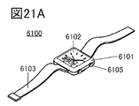
- 21A to 21F are diagrams for explaining a configuration example of an electronic device.
- the ordinal numbers “1st”, “2nd”, and “3rd” are added to avoid confusion of the components. Therefore, the number of components is not limited. Moreover, the order of the components is not limited. Further, for example, the component referred to in “first” in one of the embodiments of the present specification and the like is defined as a component referred to in “second” in another embodiment or in the claims. It is possible. Further, for example, the component mentioned in “first” in one of the embodiments of the present specification and the like may be omitted in another embodiment or in the claims.
- the power supply potential VDD may be abbreviated as potentials VDD, VDD, etc. This also applies to other components (eg, signals, voltages, circuits, elements, electrodes, wiring, etc.).
- the code is used for identification such as "_1”, “_2”, “[n]", “[m, n]”. May be added and described.
- the second wiring GL is described as wiring GL [2].
- a connector such as FPC (Flexible Printed Circuit) or TCP (Tape Carrier Package) is attached to a substrate constituting a display device, or a COG (Chip On Glass) is attached to a substrate constituting a display device.
- FPC Flexible Printed Circuit
- TCP Transmission Carrier Package
- COG Chip On Glass
- FIG. 1A is a schematic diagram for explaining the appearance of the display device 100 according to one aspect of the present invention.
- the display device of one aspect of the present invention has a configuration in which a display element and a conductive layer constituting an antenna are provided between a pair of substrates.
- the display device of one aspect of the present invention can realize the arrangement of a plurality of antennas superimposed on the display unit.
- the display device 100 includes a substrate 110 on which a display element is provided and a substrate 120 on which a conductive layer is provided.
- the substrate 110 has an FPC 112 into which a signal or the like for displaying is input.
- the substrate 120 has an FPC 122 for transmitting and receiving signals.
- the substrate 120 has a conductive layer processed into a desired shape.
- the conductive layer functions as the antenna 130. It is preferable that each conductive layer has an opening. Then, the opening and the display element are arranged so as to overlap each other. By doing so, since the light from the display element is emitted to the outside through the opening, the conductive layer that functions as an antenna does not need to have translucency. That is, as the material of the conductive layer that functions as an antenna, it is possible to apply a material such as a metal or an alloy having a lower resistance than the translucent conductive material. Therefore, wireless signals can be transmitted and received as an antenna with reduced influence of wiring resistance and the like.
- the line width can be made extremely small. That is, the surface area of the conductive layer when viewed from the display surface side (planar view) can be reduced. As a result, the influence of noise generated when the pixels are driven can be suppressed. Further, the influence of noise can be suppressed even if the conductive layer functioning as an antenna between the two substrates and the display element constituting the pixel are arranged close to each other. Therefore, the thickness of the display device can be reduced. In particular, by using a flexible material for a pair of substrates, a thin, lightweight and flexible display device can be realized.
- the conductive layer provided on the substrate 120 has a mesh-like shape having a plurality of openings.
- a material having a low resistance value is desirable.
- a metal such as silver, copper, or aluminum may be used.
- metal nanowires may be used that are constructed with a large number of very thin (eg, a few nanometers in diameter) conductors.
- Ag nanowires, Cu nanowires, Al nanowires and the like may be used.
- a light transmittance of 89% or more and a sheet resistance value of 40 ⁇ / ⁇ or more and 100 ⁇ / ⁇ or less can be realized.
- the metal nanowires may be used for electrodes used for display elements, for example, pixel electrodes and common electrodes.
- carbon nanotubes may be used as the material of the conductive layer used for the antenna 130.
- FIG. 1B is a schematic diagram for explaining the configuration on the substrate 110 side in the display device 100 of one aspect of the present invention.
- the substrate 110 has a display unit 111.
- the display unit 111 has a plurality of pixels 116 arranged in a matrix.
- the pixel 116 preferably includes a plurality of sub-pixels. Each sub-pixel includes a display element.
- a circuit 115 that is electrically connected to the pixels 116 in the display unit 111 is provided.
- As the circuit 115 for example, a circuit that functions as a gate drive circuit can be applied.
- the FPC 112 has a function of supplying a signal from the outside to at least one of the display unit 111 or the circuit 115 via the wiring 114. It is preferable to mount the IC 113 that functions as a source drive circuit on the substrate 110 or the FPC 112.
- the IC 113 can be mounted on the substrate 110 by the COG method or the COF (Chip On Film) method.
- Display elements that can be used in display devices include liquid crystal elements, organic EL elements, inorganic EL elements, LED elements, microcapsules, electrophoresis elements, electrowetting elements, electrofluidic elements, electrochromic elements, MEMS elements, and the like. Display element of can be used.
- a touch panel having a touch sensor function can also be used.
- the IC 113 may have a touch sensor controller, a sensor driver, and the like.
- the touch panel it is preferable to use an on-cell type touch panel in which a display device and a touch sensor are integrated, or an in-cell type touch panel.
- the on-cell type or in-cell type touch panel can be thin and lightweight. Further, the on-cell type or in-cell type touch panel can reduce the number of parts, so that the cost can be reduced. Further, as the touch panel, an optical type or a capacitance type touch sensor can be adopted.
- FIG. 2A is a schematic diagram for explaining the configuration on the substrate 120 side in the display device 100 of one aspect of the present invention.
- the substrate 120 has a conductive layer processed into a desired shape.
- the processed conductive layer functions as an antenna.
- a plurality of antennas 130_1 to 130_N can be provided on the substrate.
- the FPC 122 has a function as a wiring for making an electrical connection between the plurality of antennas 130_1 to 130_N and the integrated circuit 141 provided on the substrate 140.
- the antennas 130_1 to 130_N can be arranged on the substrate 120.
- a plurality of antennas 130_1 to 130_N can be arranged side by side over an area equivalent to the display unit 111 having pixels 116.
- a plurality of antennas 130_1 to 130_N can be arranged side by side over the entire surface of the substrate 120, which is wider than the area of the substrate 140. Since a plurality of antennas 130_1 to 130_N can be arranged side by side, antennas having different shapes or antennas having different sizes can be arranged side by side. Further, since the antenna can be provided in the area of the display unit, the display device can be compatible with the configuration in which a plurality of antennas are arranged side by side and the configuration in which the integrated circuit is miniaturized. ..
- antennas of different shapes or antennas of different sizes can be arranged, it is possible to configure the configuration to transmit and receive radio signals of different frequencies. Further, since a plurality of antennas having the same shape and the same size can be arranged, a beamforming technique using antennas arranged in an array can be applied. Since the antenna directivity can be provided by the beamforming technology, it is possible to compensate for the radio wave propagation loss when the communication frequency becomes high.
- the arrangement of the antennas 130_1 to 130_N for example, it is effective to arrange the antennas for 1/2 wavelength of the communication frequency, for example, at intervals of about 5 mm. It is preferable to arrange a conductive layer that does not function as an antenna between the antennas 130_1 to 130_N. By arranging a conductive layer that does not function as an antenna between adjacent antennas, it is possible to improve the coverage of the thin film formed after the step of forming the conductive layer and flatten the surface. Further, by making the thickness of the layer including the conductive layer uniform, the uneven brightness of the light from the pixels transmitted through the conductive layer can be reduced, and a display device with improved display quality can be realized.
- the conductive layer that does not function as an antenna may be used as an electrode of the touch sensor. Since the frequency of the signal used in the touch sensor is different from the frequency of the signal used in wireless communication, the signals can be separated.
- FIG. 2B illustrates the integrated circuit 141 and the baseband processor 12 in addition to the plurality of antennas 130_1 to 130_N shown in FIG. 2A.
- the integrated circuit 141 has a function of performing modulation processing or demodulation processing on the data of the radio signal transmitted / received by the antennas 130_1 to 130_N. Specifically, the integrated circuit 141 has a function of modulating the transmission data received from the baseband processor 12 with a carrier wave to generate a transmission signal, and outputting the transmission signal via the antennas 130_1 to 130_N. Further, the integrated circuit 141 has a function of receiving a received signal via the antennas 130_1 to 130_N, demodulating the received signal by a carrier wave to generate received data, and transmitting the received data to the baseband processor 12. Further, the integrated circuit 141 may include a duplexer connected to each of the antennas 130_1 to 130_N.
- the baseband processor 12 has a function of performing baseband processing including coding (for example, error correction coding) processing or decoding processing for data transmitted to and received from an external device via antennas 130_1 to 130_N. Specifically, the baseband processor 12 has a function of receiving transmission data from the application processor, performing encoding processing on the received transmission data, and transmitting the transmitted data to the integrated circuit 141. Further, the baseband processor 12 has a function of receiving received data from the integrated circuit 141, performing decoding processing on the received received data, and transmitting the received data to the application processor.
- coding for example, error correction coding
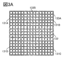
- FIG. 3A illustrates a layout diagram of the conductive layers 131A to 131D applicable to the antennas 130_1 to 130_N described with reference to FIG. 2A and the conductive layers 132 provided between the antennas.
- an opening 133A for transmitting the light of the pixel is shown in the conductive layers 131A to 131D.
- an opening 133B for transmitting the light of the pixel is illustrated.
- the conductive layers 131A to 131D that function as antennas are provided apart from the conductive layers 132 that do not function as antennas.
- the opening 133A and the opening 133B are provided in an area overlapping the pixels of the display unit. With this configuration, the light from the display element is emitted to the outside through the openings 133A and 133B, so that the conductive layers 131A to 131D do not need to have translucency. That is, as the material of the conductive layer that functions as an antenna, a material such as a metal or an alloy having a lower resistance than the translucent conductive material can be applied.
- FIG. 3B is a schematic diagram showing the layout diagram described in FIG. 3A as a block diagram for each area.
- the conductive layers 131A to 131D and the conductive layer 132 are shown in the same manner as in FIG. 3A.
- the antenna is arranged for 1/2 wavelength of the communication frequency. For example, it can be arranged at intervals of about 5 mm. Therefore, it is possible to apply a beamforming technique using antennas arranged in an array. Since the antenna directivity can be provided by the beamforming technology, it is possible to compensate for the radio wave propagation loss when the communication frequency becomes high.
- the conductive layer that functions as an antenna is regularly arranged with the conductive layer that does not function as an antenna sandwiched between them, so that the conductive layer is formed after the step of forming the conductive layer.
- the coating property of the thin film can be improved and the surface can be flattened.
- the thickness of the layer including the conductive layer uniform, the uneven brightness of the light from the pixels transmitted through the conductive layer can be reduced, and a display device with improved display quality can be realized.
- the configuration in which the conductive layers 131A to 131D are regularly arranged in a quadrangular shape is illustrated, but the present invention is not limited to this.
- the shapes of the conductive layers 131A to 131D may be circular, triangular, pentagonal, hexagonal, octagonal, or the like.
- FIG. 4A shows a schematic diagram when the sizes of the conductive layers functioning as antennas are different in the same manner as the block diagram shown in FIG. 3B. Further, FIG. 4B shows a schematic diagram showing a conductive layer that does not function as an antenna in addition to the conductive layer that functions as an antenna shown in FIG. 4A.
- FIG. 4A illustrates the conductive layers 131P, 131Q, and 131R as conductive layers of different sizes that function as antennas on the substrate 120.
- FIG. 4B in addition to the configuration shown in FIG. 4A, the conductive layer 132 is shown.
- beamforming technology using antennas arranged in an array can be applied by regularly arranging conductive layers that function as antennas with a conductive layer that does not function as an antenna in between. it can. Further, as shown in FIG. 4B, by regularly arranging the conductive layer that functions as an antenna with the conductive layer that does not function as an antenna sandwiched between them, a thin portion of the conductive layer is formed. Can be suppressed. Therefore, the coverage of the thin film formed after the step of forming the conductive layer can be improved, and the surface can be flattened.
- 5A to 5F show a configuration example of the conductive layer 131 applicable to the conductive layers 131A to 131D that function as antennas, which is shown in FIG. 3A.
- the conductive layer 131 may have an opening 133 and a notch 134.
- the conductive layer 131 may have openings 133A and 133B having different sizes.
- the conductive layer 131 may have notches 134 in addition to openings 133A and 133B having different sizes.
- the conductive layer 131 may have a protrusion 135 in addition to the opening 133.
- the conductive layer 131 may have a plurality of openings 133A and 133B having different sizes, respectively.
- the conductive layer 131 may have a configuration having an opening 133C with rounded corners. Further, as shown in FIG. 5F, the corners of the conductive layer 131 may be rounded.
- FIG. 6A an element layer that overlaps with the conductive layer 131 having the opening 133, which functions as an antenna, will be described with reference to the drawings.
- the element layer 161 having a transistor is superimposed on the conductive layer 131.
- the opening 133 overlaps with the opening 162 and the pixel 116 of the element layer 161.
- the light emitted by the pixel 116 (shown by the chain arrow in FIG. 6A) is configured to pass through the openings 162 and 133.
- FIG. 6B is a diagram for schematically explaining the overlap between the transistor and the conductive layer 131 when the region 160 on which the conductive layer 131 and the element layer 161 are superimposed shown in FIG. 6A is viewed in a plan view.
- FIG. 6B illustrates a plurality of transistors 164 connected to the wiring 163 included in the element layer 161.
- a part of the circuit included in the integrated circuit 141 described with reference to FIGS. 2A and 2B is part of the element layer 161. Can be provided in.
- a duplexer, an amplifier, a mixer, or the like can be configured by the transistor 164 that the element layer 161 has.
- the amplified signal is input / output to / from the substrate 140 having the integrated circuit 141 via the FPC 122, so that stable operation can be performed.
- the transistor included in the element layer 161 preferably has a configuration in which a transistor having an oxide semiconductor (metal oxide) in the channel forming region (hereinafter referred to as an OS transistor) is used. Since the OS transistor can be freely arranged on the element layer having a transistor having silicon (hereinafter, Si transistor) in the channel forming region, or on the element layer having an OS transistor, integration can be easily performed. it can. Further, since the OS transistor can be manufactured by using the same manufacturing apparatus as the Si transistor, it can be manufactured at low cost.
- a transistor having an oxide semiconductor (metal oxide) in the channel forming region hereinafter, Si transistor
- Si transistor silicon
- the OS transistor can be manufactured by using the same manufacturing apparatus as the Si transistor, it can be manufactured at low cost.
- In-M-Zn oxide (element M is aluminum, gallium, yttrium, copper, vanadium, beryllium, boron, titanium, iron, nickel, germanium, zirconium, molybdenum, lanthanum, cerium, neodymium, hafnium , One or more selected from tantalum, tungsten, gallium, etc.) and the like.
- a metal oxide having indium, zinc, and gallium In-Ga-Zn-based oxide
- a metal oxide having indium, zinc, and tin In-Sn-Zn-based oxide
- a metal oxide (In-Ga-Zn-Sn-based oxide) having indium, zinc, gallium, and tin can be preferably used.
- the formation of a metal oxide that functions as an oxide semiconductor may be carried out by a sputtering method or an ALD (Atomic Layer Deposition) method.
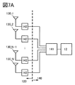
- FIG. 7A corresponds to the configuration in which the amplifier 142 is illustrated in addition to the configuration of the block diagram shown in FIG. 2B.
- the transistors 164 and the like provided in the element layer 161 in addition to the antennas 130_1 to 130_N and providing the amplifier 142 on the substrate 120 side the circuit of the integrated circuit 141 on the substrate 140 side can be miniaturized. ..
- FIG. 7B corresponds to the configuration in which the duplexer DUP is illustrated in addition to the configuration of the block diagram shown in FIG. 7A.
- the transistor 164 provided in the element layer 161 is used to provide the amplifier 142 and the duplexer DUP on the substrate 120 side, so that the circuit of the integrated circuit 141 on the substrate 140 side can be miniaturized. Can be transformed into.
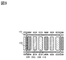
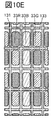
- FIGS. 9 and 10A to 10E are schematic views showing the positional relationship between the pixels and the sub-pixels included in the pixels when viewed from the display surface side, and the conductive layer 131.
- Each of the plurality of sub-pixels included in the pixel 116 includes a display element.
- Typical display elements include light emitting elements such as organic EL elements, liquid crystal elements, display elements (also referred to as electronic inks) that display by an electrophoresis method or an electronic powder fluid (registered trademark) method, and shutter type MEMS. Examples include a display element, an optical interference type MEMS display element, and the like.
- the sub-pixel may have a transistor, a capacitive element, a wiring for electrically connecting these, and the like, in addition to the display element.
- a light receiving element for example, a light receiving element using an organic photodiode
- the light emitted from the other sub pixel is received by the light receiving element, so that the display device has an imaging function or sensing. Additional functions such as functions may be provided.
- the positional relationship between the sub-pixel and the conductive layer 131 can also be applied to a transmissive liquid crystal display, a transflective liquid crystal display, a reflective liquid crystal display, a direct-view liquid crystal display, and the like.
- a part or all of the pixel electrodes may have a function as a reflective electrode.
- a part or all of the pixel electrodes may have aluminum, silver, or the like.
- a configuration suitable for the display element to be applied can be selected from various pixel circuits and used.
- one opening 133 of the conductive layer 131 and three sub-pixels of the sub-pixel 33R, the sub-pixel 33G, and the sub-pixel 33B are arranged so as to overlap each other.
- the opening 133 of the conductive layer 131 is arranged so as to overlap one pixel 116.
- the spacing between the pixels 116 and the spacing between the grids of the conductive layer 131 are the same.
- FIG. 8B shows an example in which one opening 133 and one sub-pixel are arranged so as to overlap each other.
- the wiring resistance of the conductive layer 131 can be reduced by arranging the conductive layer 131 between the two sub-pixels included in one pixel 116 in a plan view.
- the reception sensitivity of the antenna can be improved.
- FIG. 8C shows an example in which the pixel 116 further has the sub-pixel 33Y as compared with the configuration shown in FIG. 8A.
- the sub-pixel 33Y for example, a pixel capable of displaying yellow can be applied.
- a pixel capable of displaying white can be applied.
- FIG. 8D shows an example in which one opening 133 and one sub-pixel are arranged so as to overlap each other. That is, an example is shown in which the conductive layer 131 is arranged between two adjacent sub-pixels in a plan view. Although not shown, the configuration may be such that two of the four sub-pixels are arranged so as to overlap one opening 133.
- FIGS. 8E to 8G show an example in which each sub-pixel is arranged in a stripe shape.
- FIGS. 8E to 8G sub-pixels of two colors are alternately arranged in one direction. May be.
- FIG. 8E shows a configuration in which a pixel 116 having four sub-pixels and one opening 133 overlap each other.
- FIG. 8F shows a configuration in which two adjacent sub-pixels and one opening 133 overlap each other.
- FIG. 8G shows a configuration in which one sub-pixel and one opening 133 overlap each other.
- the size of the sub-pixels of the pixel 116 may be different for each sub-pixel.
- the sub-pixel showing blue having a relatively low luminosity factor can be made large, and the sub-pixel showing green or red having a relatively high luminosity factor can be made small.
- 10A and 10B show an example in which the size of the sub-pixel 33B is larger than that of the other sub-pixels among the sub-pixel 33R, the sub-pixel 33G, and the sub-pixel 33B.
- the sub-pixels 33R and the sub-pixels 33G are arranged alternately is shown, but as shown in FIG. 8A and the like, each of the three sub-pixels is arranged in a stripe shape, and the sizes of the sub-pixels are different. It can also be configured.
- FIG. 10A shows a configuration in which a pixel 116 having three sub-pixels and one opening 133 overlap each other. Further, in FIG. 10B, one opening 133 and one sub-pixel 33B overlap each other, and the other one opening 133 and two sub-pixels (sub-pixel 33R and sub-pixel 33G) overlap each other. ..
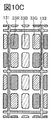
- FIG. 10C shows a configuration in which six sub-pixels, two for each color, and one opening 133 overlap each other.
- FIG. 10D shows a configuration in which three sub-pixels, one for each color, and one opening 133 overlap each other.
- FIG. 10E shows a configuration in which one sub-pixel and one opening 133 overlap each other.
- the configuration is not limited to the configuration shown here, and two or more adjacent sub-pixels and one opening 133 may overlap each other.
- Embodiment 2 a configuration example of an electronic device including the display device 100 shown in the above embodiment will be described with reference to FIGS. 11 and 12.
- a smartphone will be described as an example of the electronic device, but other electronic devices such as a portable game terminal, a tablet PC (Personal Computer), and a notebook PC may be used. Further, the electronic device according to the present embodiment can be applied to other electronic devices capable of performing wireless communication.
- the antenna 130 is provided according to the frequency band corresponding to the 5G communication standard. As described in the first embodiment, since the antennas can be arranged so as to be superimposed on the display unit of the display device, a plurality of antennas corresponding to a plurality of frequency bands can be arranged.
- the power management IC 16 has a function of generating an internal power source from the battery 15 or an external power source. This internal power supply is provided to each block of the electronic device 10. At this time, the power management IC 16 has a function of controlling the voltage of the internal power supply for each block to be supplied with the internal power supply. The power management IC 16 controls the voltage of the internal power supply based on the instruction from the application processor 11. Further, the power management IC 16 can also control the supply and cutoff of the internal power supply for each block. The power management IC 16 also has a function of controlling charging of the battery 15 when an external power source is supplied.
- the camera unit 18 has a function of acquiring an image according to an instruction from the application processor 11.
- the operation input unit 19 has a function as a user interface for the user to operate and give an operation instruction to the electronic device 10.
- the audio IC 20 has a function of decoding the voice data transmitted from the application processor 11 and driving the speaker 22.
- the audio IC 20 has a function of encoding the voice information obtained from the microphone 21 to generate voice data and outputting the voice data to the application processor 11.
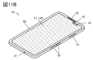
- the display unit 17 housed in the housing 50 functions as an antenna 130. Further, in FIG. 11B, the camera unit 18, the operation input unit 19, the microphone 21 and the speaker 22 shown in FIG. 11A are shown.
- the display unit 17 occupies most of the housing 50. Therefore, the communication distance is configured by arranging a conductive layer that functions as an antenna on a substrate that serves as a display unit, and arranging an element layer having a transistor or the like superimposed on the conductive layer. It is possible to extend the size and reduce the size of the integrated circuit.
- FIG. 12 is a block diagram for explaining a configuration example of the integrated circuit 141.
- the integrated circuit 141 shown in FIG. 12 includes a low-noise amplifier 31, a mixer 32, a low-pass filter 33, a variable gain amplifier 34, an analog-to-digital conversion circuit 35, an interface unit 36, a digital-to-analog conversion circuit 41, a variable gain amplifier 42, and a low-pass filter 43. It has a mixer 44, a power amplifier 45, and an oscillation circuit 40. Further, in FIG. 12, the antenna 130, the duplexer DUP, and the baseband processor 12 are also shown.
- the low-noise amplifier 31, mixer 32, low-pass filter 33, variable gain amplifier 34, analog-to-digital conversion circuit 35 are receiving circuit blocks, digital-to-analog conversion circuit 41, variable gain amplifier 42, low-pass filter 43, mixer 44, and power amplifier 45 are transmitting. Sometimes called a circuit block.
- the digital-to-analog conversion circuit 41 converts the digital signal received by the interface unit 36 into an analog signal.
- the variable gain amplifier 42 amplifies the output signal of the digital-to-analog conversion circuit 41.
- the low-pass filter 43 removes unnecessary high-frequency components in the signal from the variable gain amplifier 42.
- the mixer 44 modulates and up-converts (frequency conversion) the analog signal using the signal of the oscillation circuit 40.
- the power amplifier 45 amplifies the output signal of the mixer 44 with a predetermined gain and outputs it.
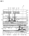
- the transistor 201 has a semiconductor layer 216, an insulating layer 220, a conductive layer 221, a conductive layer 217, a conductive layer 213, an insulating layer 215, an insulating layer 214, and the like.
- An insulating layer 211 is provided on the substrate 110.
- the insulating layer 211 functions as a barrier layer that prevents impurities such as water and hydrogen from diffusing from the substrate 110 into the transistor 201 and oxygen from the semiconductor layer 216 toward the insulating layer 211.
- a film such as an aluminum oxide film, a hafnium oxide film, or a silicon nitride film, in which hydrogen and oxygen are less likely to diffuse than the silicon oxide film, can be used.
- the semiconductor layer 216 preferably has a metal oxide (oxide semiconductor) film having semiconductor characteristics.
- the pair of conductive layers 217 are provided apart on the semiconductor layer 216.
- the conductive layer 217 functions as a source electrode and a drain electrode.
- an insulating layer 218 is provided so as to cover the semiconductor layer 216 and the conductive layer 217, and an insulating layer 219 is provided on the insulating layer 218.
- the insulating layer 218 and the insulating layer 219 are provided with an opening reaching the semiconductor layer 216, and the insulating layer 220 and the conductive layer 221 are embedded inside the opening.
- an insulating layer 224 is provided so as to cover the upper surfaces of the insulating layer 219, the conductive layer 221 and the insulating layer 220.
- the plug electrically connected to the conductive layer 217 is provided inside the openings provided in the insulating layer 225, the insulating layer 224, the insulating layer 219, and the insulating layer 218.
- the plug preferably has a conductive layer 222 in contact with the side surface of the opening and the upper surface of the conductive layer 217, and a conductive layer 223 embedded inside the conductive layer 222. At this time, it is preferable to use a conductive material as the conductive layer 222, in which hydrogen and oxygen are difficult to diffuse.
- the light emitting element that can be used for the light emitting element 202 an element capable of self-luminous light can be used, and an element whose brightness is controlled by a current or a voltage is included in the category.
- LEDs, organic EL elements, inorganic EL elements and the like can be used.
- Either a low molecular weight compound or a high molecular weight compound can be used for the EL layer 228, and an inorganic compound may be contained.
- the layers constituting the EL layer 228 can be formed by a method such as a thin-film deposition method (including a vacuum vapor deposition method), a transfer method, a printing method, an inkjet method, or a coating method, respectively.
- the emission spectrum of the material having a peak in the yellow wavelength region is preferably a material having a spectral component also in the green and red wavelength regions.
- the light emitting element 202 may be a single element having one EL layer, or may be a tandem element in which a plurality of EL layers are laminated via a charge generation layer.
- the above-mentioned light emitting layer and the layer containing a substance having a high hole injecting property, a substance having a high hole transporting property, a substance having a high electron transporting property, a substance having a high electron injecting property, a bipolar substance, and the like are Each of them may have an inorganic compound such as a quantum dot or a polymer compound (oligoform, dendrimer, polymer, etc.). For example, by using quantum dots in the light emitting layer, it can function as a light emitting material.
- a colloidal quantum dot material an alloy type quantum dot material, a core / shell type quantum dot material, a core type quantum dot material, or the like can be used. Further, a material containing an element group of groups 12 and 16, 13 and 15 or 14 and 16 may be used. Alternatively, a quantum dot material containing elements such as cadmium, selenium, zinc, sulfur, phosphorus, indium, tellurium, lead, gallium, arsenide, and aluminum may be used.
- the light emitted from the light emitting element 202 is absorbed by the colored layer and has a wavelength other than a predetermined wavelength, and is emitted to the outside as, for example, red light, green light, or blue light.
- the colored layer the above-mentioned quantum dot material may be used.
- color conversion wavelength conversion
- the manufacturing cost can be reduced, which is preferable.
- a photodiode which is a light receiving element
- a photodiode may be provided on the same layer as the light emitting element 202. With this configuration, it is possible to impart the function of a touch sensor to the display device.
- the active layer of the light receiving element a laminated structure in which a p-type semiconductor and an n-type semiconductor are laminated to realize a pn junction, or a p-type semiconductor, an i-type semiconductor, and an n-type semiconductor are laminated to realize a pin junction. It can be a laminated structure or the like.
- an inorganic semiconductor such as silicon or an organic semiconductor containing an organic compound can be used.
- an organic semiconductor material because the EL layer 228 of the light emitting element 202 and the active layer of the light receiving element can be easily formed by a vacuum vapor deposition method, and the manufacturing apparatus can be shared.
- an electron-accepting organic semiconductor material such as fullerene (for example, C 60 , C 70, etc.) or a derivative thereof can be used as the material of the n-type semiconductor.
- an electron-donating organic semiconductor material such as copper (II) phthalocyanine (CuPc) or tetraphenyldibenzoperiversene (DBP) can be used. ..
- the active layer of the light receiving element may have a laminated structure (pn laminated structure) of an electron-accepting semiconductor material and an electron-donating semiconductor material, or an electron-accepting semiconductor material and an electron-donating semiconductor material between them.
- a laminated structure (p-n laminated structure) in which a bulk heterostructure layer in which a semiconductor material is co-deposited is provided may be used. Further, for the purpose of suppressing dark current when not irradiating light, a layer that functions as a hole block layer around (upper or lower) the above-mentioned pn laminated structure or p-in laminated structure. Alternatively, a layer that functions as an electronic block layer may be provided.
- An insulating layer 231 and an insulating layer 232 are laminated and provided on the light emitting element 202 so as to cover the light emitting element 202. These two insulating layers function as a protective layer that prevents impurities such as water from diffusing into the light emitting element 202.
- an inorganic insulating film having low moisture permeability such as a silicon oxide film, a silicon nitride film, or an aluminum oxide film.
- an organic insulating film having high translucency can be used for the insulating layer 232.
- the influence of the uneven shape on the lower side of the insulating layer 232 can be alleviated, and the surface of the insulating layer 232 can be made a smooth surface. As a result, the adhesion when bonded to the element layer 161 can be improved.
- the transistor 203 has a semiconductor layer 305, an insulating layer 309, a conductive layer 310, a conductive layer 306, a conductive layer 303, an insulating layer 304, an insulating layer 302, and the like.
- the description of the semiconductor layer 305, the insulating layer 309, the conductive layer 310, the conductive layer 306, the conductive layer 303, the insulating layer 304, and the insulating layer 302 in the transistor 203 describes the semiconductor layer 216, the insulating layer 220, the conductive layer 221 and the conductive layer in the transistor 201. This is the same as the layer 217, the conductive layer 213, the insulating layer 215, and the insulating layer 214.
- the insulating layer 301 having a configuration other than the transistor 203 is the same as the description of the insulating layer 211.
- the insulating layer 307, the insulating layer 308, the insulating layer 311 and the insulating layer 312 are the same as the description of the insulating layer 218, the insulating layer 219, the insulating layer 224, and the insulating layer 225, respectively.
- the insulating layer 307 is the same as the description of the insulating layer 218.
- the conductive layer 313 and the conductive layer 314 are the same as the description of the conductive layer 222 and the conductive layer 223, respectively.
- the conductive layer 316 provided on the insulating layer 315 and the conductive layer 318 provided on the insulating layer 317 function as wiring for electrically connecting the transistor 203 and the conductive layer 320 or the conductive layer 321.
- the conductive layer 320 provided on the insulating layer 319 functions as an antenna.
- the conductive layer 321 provided on the insulating layer 319 functions as wiring.
- the conductive layer 320 and the conductive layer 321 are preferably arranged at positions that do not overlap with the light emitting element 202 so that the light from the light emitting element 202 is emitted toward the display surface side.
- the transistor 203 can have an insulating layer 301 formed on a substrate provided with a separately prepared release layer, and can be formed on the insulating layer 301 in the same manner as the transistor 201.
- the substrate 120 provided with the element layer 161 and the conductive layer 131 can be peeled off at the peeling surface provided on the peeling layer and bonded to the substrate 110 side.
- the substrate 110 and the substrate 120 may be adhered using an adhesive layer provided on the outer periphery of the substrate.
- a translucent substrate such as a glass substrate, a quartz substrate, a sapphire substrate, or a plastic substrate can be used. Further, the substrate 120 can be used as a flexible display device by forming a flexible substrate together with the substrate 110.
- the transistor has a conductive layer that functions as a gate electrode, a semiconductor layer, a conductive layer that functions as a source electrode, a conductive layer that functions as a drain electrode, and an insulating layer that functions as a gate insulating layer.
- Transistors using metal oxides which have a wider bandgap and a lower carrier density than silicon, retain the charge accumulated in the capacitive element connected in series with the transistor for a long period of time due to its low off-current. Is possible.
- the atomic number ratio of the metal element of the sputtering target used for forming the In-M-Zn oxide is In ⁇ M, Zn. It is preferable to satisfy ⁇ M.
- the atomic number ratio of the semiconductor layer to be formed includes a variation of plus or minus 40% of the atomic number ratio of the metal element contained in the sputtering target.
- an oxide semiconductor having an appropriate composition may be used according to the required semiconductor characteristics and electrical characteristics (field effect mobility, threshold voltage, etc.) of the transistor. Further, in order to obtain the required semiconductor characteristics of the transistor, it is preferable that the carrier density, impurity concentration, defect density, atomic number ratio of metal element and oxygen, interatomic distance, density, etc. of the semiconductor layer are appropriate. ..
- the concentration of silicon or carbon in the semiconductor layer is set to 2 ⁇ 10 18 atoms / cm 3 or less, preferably 2 ⁇ 10 17 atoms / cm 3 or less.
- the concentration of the alkali metal or alkaline earth metal obtained by the secondary ion mass spectrometry in the semiconductor layer is set to 1 ⁇ 10 18 atoms / cm 3 or less, preferably 2 ⁇ 10 16 atoms / cm 3 or less.
- the nitrogen concentration obtained by the secondary ion mass spectrometry in the semiconductor layer is preferably 5 ⁇ 10 18 atoms / cm 3 or less.
- Oxide semiconductors are divided into single crystal oxide semiconductors and non-single crystal oxide semiconductors.
- Examples of the non-single crystal oxide semiconductor include CAAC-OS (c-axis-aligned crystalline semiconductor), polycrystalline oxide semiconductor, nc-OS (nanocrystalline oxide semiconductor), and pseudoamorphic oxide semiconductor (a-like). : Amorphous-like oxide semiconductor), amorphous oxide semiconductors, and the like.
- the above-mentioned non-single crystal oxide semiconductor or CAC-OS can be preferably used. Further, as the non-single crystal oxide semiconductor, nc-OS or CAAC-OS can be preferably used.
- CAC-OS As the semiconductor layer of the transistor, it is preferable to use CAC-OS as the semiconductor layer of the transistor.
- CAC-OS high electrical characteristics or high reliability can be imparted to the transistor.
- Two or more types of semiconductor layers are included in the CAAC-OS region, the polycrystalline oxide semiconductor region, the nc-OS region, the pseudo-amorphous oxide semiconductor region, and the amorphous oxide semiconductor region. It may be a mixed film having.
- the mixed film may have, for example, a single-layer structure or a laminated structure including any two or more of the above-mentioned regions.
- CAC Cloud-Linked Company
- CAC-OS is, for example, a composition of a material in which elements constituting a metal oxide are unevenly distributed in a size of 0.5 nm or more and 10 nm or less, preferably 1 nm or more and 2 nm or less, or a size close thereto.
- the metal oxide one or more metal elements are unevenly distributed, and the region having the metal element is 0.5 nm or more and 10 nm or less, preferably 1 nm or more and 2 nm or less, or a size in the vicinity thereof.
- the state of being mixed with is also called a mosaic shape or a patch shape.
- the metal oxide preferably contains at least indium. In particular, it preferably contains indium and zinc. Also, in addition to them, aluminum, gallium, yttrium, copper, vanadium, beryllium, boron, silicon, titanium, iron, nickel, germanium, zirconium, molybdenum, lantern, cerium, neodymium, hafnium, tantalum, tungsten, or magnesium, etc. One or more selected from the above may be included.
- GaO X3 (X3 is a real number larger than 0)
- gallium zinc oxide hereinafter, Ga X4 Zn Y4 O Z4 (X4, Y4, and Z4 are real numbers larger than 0)
- the material is separated into a mosaic-like structure, and the mosaic-like InO X1 or In X2 Zn Y2 O Z2 is uniformly distributed in the film (hereinafter, also referred to as cloud-like). is there.
- CAC-OS relates to the material composition of metal oxides.
- CAC-OS is a region that is partially observed as nanoparticles containing Ga as a main component and nanoparticles containing In as a main component in a material composition containing In, Ga, Zn, and O. The regions observed in the shape are randomly dispersed in a mosaic pattern. Therefore, in CAC-OS, the crystal structure is a secondary element.
- CAC-OS does not include a laminated structure of two or more types of films having different compositions.
- CAC-OS has a region observed in the form of nanoparticles containing the metal element as a main component and a nano having In as a main component.
- the regions observed in the form of particles refer to a configuration in which the regions are randomly dispersed in a mosaic pattern.
- CAC-OS can be formed by a sputtering method, for example, under the condition that the substrate is not intentionally heated.
- a sputtering method one or more selected from an inert gas (typically argon), an oxygen gas, and a nitrogen gas may be used as the film forming gas.
- an inert gas typically argon
- an oxygen gas typically a nitrogen gas
- a nitrogen gas may be used as the film forming gas.
- the flow rate ratio of the oxygen gas is preferably 0% or more and less than 30%, preferably 0% or more and 10% or less. ..
- CAC-OS is characterized by the fact that no clear peak is observed when measured using the ⁇ / 2 ⁇ scan by the Out-of-plane method, which is one of the X-ray diffraction (XRD) measurement methods. Have. That is, from the X-ray diffraction measurement, it can be seen that the orientation of the measurement region in the ab plane direction and the c-axis direction is not observed.
- XRD X-ray diffraction
- a region in which GaO X3 is a main component is obtained by EDX mapping acquired by using energy dispersive X-ray spectroscopy (EDX: Energy Dispersive X-ray spectroscopy).
- EDX Energy Dispersive X-ray spectroscopy
- CAC-OS has a structure different from that of the IGZO compound in which metal elements are uniformly distributed, and has properties different from those of the IGZO compound. That is, the CAC-OS is phase-separated into a region containing GaO X3 or the like as a main component and a region containing In X2 Zn Y2 O Z2 or InO X1 as a main component, and a region containing each element as a main component. Has a mosaic-like structure.
- the region in which In X2 Zn Y2 O Z2 or InO X1 is the main component is a region having higher conductivity than the region in which GaO X3 or the like is the main component. That is, when the carrier flows through the region where In X2 Zn Y2 O Z2 or InO X1 is the main component, conductivity as a metal oxide is exhibited. Therefore, a high field effect mobility ( ⁇ ) can be realized by distributing the region containing In X2 Zn Y2 O Z2 or InO X1 as the main component in the metal oxide in a cloud shape.
- the region in which GaO X3 or the like is the main component is a region having higher insulating property than the region in which In X2 Zn Y2 O Z2 or InO X1 is the main component. That is, since the region containing GaO X3 or the like as the main component is distributed in the metal oxide, the leak current can be suppressed and a good switching operation can be realized.
- CAC-OS when CAC-OS is used for a semiconductor element, the insulation property caused by GaO X3 and the like and the conductivity caused by In X2 Zn Y2 O Z2 or InO X1 act in a complementary manner, resulting in high efficiency.
- On-current (I on ) and high field-effect mobility ( ⁇ ) can be achieved.
- a transistor having CAC-OS in the semiconductor layer has high field effect mobility and high drive capability
- the transistor can be used in a drive circuit, typically a scanning line drive circuit that generates a gate signal.
- a display device having a narrow frame width (also referred to as a narrow frame) can be provided. Further, by using the transistor in the signal line drive circuit of the display device (particularly, the demultiplexer connected to the output terminal of the shift register of the signal line drive circuit), the number of wires connected to the display device is small.
- a display device can be provided.
- a transistor having CAC-OS in the semiconductor layer does not require a laser crystallization step like a transistor using low temperature polysilicon. Therefore, it is possible to reduce the manufacturing cost even for a display device using a large area substrate. Further, in a large display device having a high resolution such as ultra high definition ("4K resolution”, “4K2K”, “4K”) and super high definition (“8K resolution”, “8K4K”, “8K”).
- a transistor having CAC-OS in the semiconductor layer for the drive circuit and the display unit, writing in a short time is possible and display defects can be reduced, which is preferable.
- Materials that can be used for conductive layers such as the gates, sources and drains of transistors, as well as various wiring and electrodes that make up display devices include aluminum, titanium, chromium, nickel, copper, yttrium, zirconium, molybdenum, and silver. Examples thereof include a metal such as tantanium or tungsten, or an alloy containing this as a main component. Further, a film containing these materials can be used as a single layer or as a laminated structure.
- a single-layer structure of an aluminum film containing silicon a two-layer structure in which an aluminum film is laminated on a titanium film, a two-layer structure in which an aluminum film is laminated on a tungsten film, and a copper film on a copper-magnesium-aluminum alloy film.
- each insulating layer examples include resins such as acrylic and epoxy, resins having a siloxane bond, and inorganic insulation such as silicon oxide, silicon oxide nitride, silicon nitride oxide, silicon nitride, and aluminum oxide. Materials can also be used.
- the light emitting element is provided between a pair of insulating films having low water permeability. As a result, it is possible to suppress the intrusion of impurities such as water into the light emitting element, and it is possible to suppress a decrease in the reliability of the device.
- the insulating film having low water permeability examples include a film containing nitrogen and silicon such as a silicon nitride film and a silicon oxide film, and a film containing nitrogen and aluminum such as an aluminum nitride film. Further, a silicon oxide film, a silicon nitride film, an aluminum oxide film or the like may be used.
- water vapor permeability of less water permeable insulating film 1 ⁇ 10 -5 [g / (m 2 ⁇ day)] or less, preferably 1 ⁇ 10 -6 [g / ( m 2 ⁇ day)] or less, It is more preferably 1 ⁇ 10 -7 [g / (m 2 ⁇ day)] or less, and even more preferably 1 ⁇ 10 -8 [g / (m 2 ⁇ day)] or less.
- the release layer 331 is formed on the production substrate 330, and the insulating layer 301 which is the layer to be peeled is formed on the release layer 331.
- the element layer 161 and the conductive layer 131 are provided on the insulating layer 301.
- the conductive layer 320 and the conductive layer 321 in the conductive layer 131 are covered with the insulating layer 319A as shown in FIG. 14A.
- the insulating layer 319A corresponds to the insulating layer 319.
- the tungsten oxide film can be directly formed without forming the tungsten film.
- a sufficiently thin tungsten film is subjected to plasma treatment with a gas containing oxygen, annealing treatment is performed in a gas atmosphere containing oxygen, or oxidation is performed in a gas atmosphere containing oxygen by a method such as sputtering.
- a method such as sputtering.
- a tungsten film having a thickness of 0.1 nm or more and less than 200 nm can be used on the substrate.
- a film containing molybdenum, titanium, vanadium, tantalum, silicon, aluminum, or an alloy thereof may be used in addition to the tungsten film. Further, a laminated structure of these films and an oxide film thereof may be used.
- the release layer 331 is not limited to the inorganic film, and an organic film such as polyimide may be used.
- the substrate 120 can be attached to the flattened surfaces of the exposed conductive layer 320 and the conductive layer 321.
- a translucent substrate such as a glass substrate, a quartz substrate, a sapphire substrate, or a plastic substrate can be used.
- the substrate 120 can be used as a flexible display device by forming a flexible substrate (flexible substrate) together with the substrate 110.
- FIG. 17B is a cross-sectional view of the electronic device 400 shown in FIG. 17A in X1-X2.
- a display device having the folded substrate 110 and the substrate 120 is housed in the housing 402.
- the housing 402 there is a substrate 140 connected to the display device.
- the housing 402 protects the display device and the like from stress applied from the outside.
- the electronic device 400A provided with the display device of one aspect of the present invention has a display device 401 housed in a foldable housing 402 as shown in FIG. Since both the housing 402 and the display device 401 are foldable display devices, the foldable electronic device 400A can be used.
- the electronic device 400A has a substrate 110 and a substrate 120 provided along the housing 402.
- the display device 401 can be provided regardless of the shape of the electronic device 400A. Therefore, the area where the conductive layer that functions as an antenna is arranged can be increased.
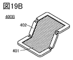
- the electronic device 400B shown in FIG. 19A can be expanded or contracted in the area of the display unit of the display device by changing the shape shown in FIG. 19B to the shape shown in FIG. 19C. Therefore, the number of conductive layers that function as antennas arranged side by side on the substrate of the display device can be adjusted. For example, it is possible to increase the reception sensitivity when the tablet is shaped as compared with the folded state. Therefore, electronic devices having different reception sensitivities can be obtained according to the change in shape.
- FIG. 20 is a top view of the touch panel 500 illustrated in this embodiment. For clarity, typical components are shown in FIG. In FIG. 20, the conductive layer is shown as a hatched electrode, but as in FIG. 3A, the conductive layer has an opening in the region overlapping the pixels. Therefore, the conductive layer shown in FIG. 20 has translucency.
- the layers Y1 to Y3 are provided.
- the conductive layers X1 to X3 and the conductive layers Y1 to Y3 are arranged so as to fill the space between 131s that function as antennas 130 provided at equal intervals. With this configuration, the area of the region where the conductive layer is not provided can be reduced, the unevenness of the transmittance can be reduced, and the function of the touch sensor can be imparted to the substrate 120 side.
- the conductive layer that functions as the electrode of the touch sensor between the adjacent antennas it is possible to prevent the formation of a thin portion of the layer including the conductive layer. Therefore, the coverage of the thin film formed after the step of forming the conductive layer can be improved, and the surface can be flattened.
- antennas having different shapes or different shapes can be arranged between the conductive layers X1 to X3 and the conductive layers Y1 to Y3 that function as electrodes of the touch panel. Therefore, the configuration can be configured to transmit and receive radio signals of different frequencies. Further, since a plurality of antennas having the same shape and the same size can be arranged, a beamforming technique using antennas arranged in an array can be applied. Since the antenna directivity can be provided by the beamforming technology, it is possible to compensate for the radio wave propagation loss when the communication frequency becomes high.
- FIG. 20 illustrates a configuration in which the conductive layers 131 are regularly arranged in a square shape, but the present invention is not limited to this.
- the shape of the conductive layer 131 may be circular, triangular, pentagonal, hexagonal, octagonal, or the like.
- each of the conductive layers X1 to X3 and the conductive layers Y1 to Y3 is given to scan the pulse voltage, and the value of the current flowing through itself at that time is detected. Since the magnitude of the current changes when the object to be detected approaches, the position information of the object to be detected can be acquired by detecting this difference. Further, in the case of the projection type mutual capacitance method, one of the conductive layers X1 to X3 and the conductive layers Y1 to Y3 is given to scan the pulse voltage, and the detected object is detected by detecting the current flowing through the other. Get the location information of.
- intersections of the conductive layers X1 to X3 and the conductive layers Y1 to Y3 are connected via a conductive layer provided in another layer.
- the area of the intersection of the conductive layers X1 to X3 and the conductive layers Y1 to Y3 is preferably shaped to be as small as possible.
- a display device such as a television or a monitor, a lighting device, a desktop or notebook type personal computer, a word processor, or a recording medium such as a DVD (Digital
- Image playback device portable CD player, radio, tape recorder, headphone stereo, stereo, table clock, wall clock, cordless telephone handset, transceiver, mobile phone, car phone, portable game machine, Large game machines such as tablet terminals and pachinko machines, calculators, portable information terminals (also called “portable information terminals"), electronic notebooks, electronic book terminals, electronic translators, voice input devices, video cameras, digital stills High-frequency heating devices such as cameras, electric shavers, and refrigerators, electric rice cookers, electric washing machines, electric vacuum cleaners, water heaters, fans, hair dryers, air conditioners, humidifiers, dehumidifiers, and other air conditioning equipment, dishwashers, etc.
- Examples thereof include tableware dryers, clothes dryers, duvet dryers, electric refrigerators, electric freezers, electric refrigerators and freezers, DNA storage freezers, tools such as flashlights and chainsaws, smoke detectors, and medical equipment such as dialysis machines. Further examples include industrial equipment such as guide lights, traffic lights, conveyor belts, elevators, escalators, industrial robots, power storage systems, and power storage devices for power leveling and smart grids.
- the display device can be used for a display unit and a communication device built in these electronic devices.
- Electronic devices include sensors (force, displacement, position, velocity, acceleration, angular velocity, rotation speed, distance, light, liquid, magnetism, temperature, chemicals, voice, time, hardness, electric field, current, voltage, power, radiation, It may have a function of measuring flow rate, humidity, inclination, vibration, odor or infrared rays).
- the electronic device can have various functions. For example, a function to display various information (still images, moving images, text images, etc.) on the display unit, a touch panel function, a function to display a calendar, date or time, a function to execute various software (programs), wireless communication. It can have a function, a function of reading a program or data recorded on a recording medium, and the like.
- 21A to 21F show an example of an electronic device.
- FIG. 21A shows an example of a wristwatch-type mobile information terminal.
- the mobile information terminal 6100 includes a housing 6101, a display unit 6102, a band 6103, an operation button 6105, and the like.
- the display device By using the display device according to one aspect of the present invention for the display unit 6102, the size of the portable information terminal 6100 can be reduced.
- FIG. 21B shows an example of a mobile phone.
- the personal digital assistant 6200 includes an operation button 6203, a speaker 6204, a microphone 6205, and the like, in addition to the display unit 6202 incorporated in the housing 6201.
- the mobile information terminal 6200 includes a fingerprint sensor 6209 in an area overlapping the display unit 6202.
- the fingerprint sensor 6209 may be an organic light sensor. Since the fingerprint differs depending on the individual, the fingerprint sensor 6209 can acquire the fingerprint pattern and perform personal authentication.
- the light emitted from the display unit 6202 can be used as a light source for acquiring the fingerprint pattern by the fingerprint sensor 6209.
- the display device By using the display device according to one aspect of the present invention for the display unit 6202, it is possible to reduce the size of the portable information terminal 6200.
- FIG. 21C shows an example of a cleaning robot.
- the cleaning robot 6300 has a display unit 6302 arranged on the upper surface of the housing 6301, a plurality of cameras 6303 arranged on the side surface, a brush 6304, an operation button 6305, various sensors, and the like. Although not shown, the cleaning robot 6300 is provided with tires, suction ports, and the like. The cleaning robot 6300 is self-propelled, can detect dust 6310, and can suck dust from a suction port provided on the lower surface.
- the cleaning robot 6300 can analyze the image taken by the camera 6303 and determine the presence or absence of obstacles such as walls, furniture, and steps. Further, when an object that is likely to be entangled with the brush 6304 such as wiring is detected by image analysis, the rotation of the brush 6304 can be stopped.
- the cleaning robot 6300 can be miniaturized.
- FIG. 21D shows an example of a robot.
- the robot 6400 shown in FIG. 21D includes an arithmetic unit 6409, an illuminance sensor 6401, a microphone 6402, an upper camera 6403, a speaker 6404, a display unit 6405, a lower camera 6406, an obstacle sensor 6407, and a moving mechanism 6408.
- the microphone 6402 has a function of detecting the user's voice, environmental sound, and the like. Further, the speaker 6404 has a function of emitting sound. The robot 6400 can communicate with the user by using the microphone 6402 and the speaker 6404.
- the display unit 6405 has a function of displaying various information.
- the robot 6400 can display the information desired by the user on the display unit 6405.
- the display unit 6405 may be equipped with a touch panel. Further, the display unit 6405 may be a removable information terminal, and by installing the display unit 6405 at a fixed position of the robot 6400, charging and data transfer are possible.
- the display unit 6405 is provided with an illuminance sensor, a camera, operation buttons, etc., and the display unit 6405 can be touch-operated with a stylus pen or the like.
- Functions of the display unit 6405 include voice call, video call, e-mail, notebook, Internet connection, music playback, and the like.
- the upper camera 6403 and the lower camera 6406 have a function of photographing the surroundings of the robot 6400. Further, the obstacle sensor 6407 can detect the presence or absence of an obstacle in the traveling direction when the robot 6400 moves forward by using the moving mechanism 6408. The robot 6400 can recognize the surrounding environment and move safely by using the upper camera 6403, the lower camera 6406, and the obstacle sensor 6407.
- the light emitting device of one aspect of the present invention can be used for the display unit 6405.
- the robot 6400 can be miniaturized.
- FIG. 21E shows an example of a television receiver.
- the television receiver 6500 shown in FIG. 21E includes a housing 6501, a display unit 6502, a speaker 6503, and the like.
- the display device By using the display device according to one aspect of the present invention for the display unit 6502, it is possible to reduce the size of the television receiver 6500.
- FIG. 21F shows an example of an automobile.
- the automobile 7160 has an engine, tires, brakes, a steering device, a camera, and the like.
- the automobile 7160 is provided with a display device according to one aspect of the present invention inside.
- the display device according to one aspect of the present invention in the automobile 7160 the automobile 7160 can function as an IoT device and the display device can be miniaturized.
- the content described in one embodiment is another content (may be a part of the content) described in the embodiment, and / or one or more. It is possible to apply, combine, or replace the contents described in another embodiment (some contents may be used).
- figure (which may be a part) described in one embodiment is another part of the figure, another figure (which may be a part) described in the embodiment, and / or one or more.
- figures (which may be a part) described in another embodiment of the above more figures can be constructed.
- the components are classified by function and shown as blocks independent of each other.
- it is difficult to separate the components for each function and there may be a case where a plurality of functions are involved in one circuit or a case where one function is involved in a plurality of circuits. Therefore, the blocks in the block diagram are not limited to the components described in the specification, and can be appropriately paraphrased according to the situation.
- the size, the thickness of the layer, or the area is shown in an arbitrary size for convenience of explanation. Therefore, it is not necessarily limited to that scale. It should be noted that the drawings are schematically shown for the sake of clarity, and are not limited to the shapes or values shown in the drawings. For example, it is possible to include variations in signal, voltage, or current due to noise, or variations in signal, voltage, or current due to timing lag.
- one of the source and the drain is referred to as "one of the source or the drain” (or the first electrode or the first terminal), and the other of the source and the drain. Is described as “the other of the source or drain” (or the second electrode, or the second terminal). This is because the source and drain of the transistor change depending on the structure or operating conditions of the transistor.
- the names of the source and drain of the transistor can be appropriately paraphrased according to the situation, such as the source (drain) terminal and the source (drain) electrode.
- electrode and “wiring” in the present specification and the like do not functionally limit these components.
- an “electrode” may be used as part of a “wiring” and vice versa.
- the terms “electrode” and “wiring” include the case where a plurality of “electrodes” and “wiring” are integrally formed.
- the voltage and the potential can be paraphrased as appropriate.
- the voltage is a potential difference from a reference potential.
- the reference potential is a ground voltage (ground voltage)
- the voltage can be paraphrased as a potential.
- the ground potential does not necessarily mean 0V.
- the electric potential is relative, and the electric potential given to the wiring or the like may be changed depending on the reference electric potential.
- a node can be paraphrased as a terminal, a wiring, an electrode, a conductive layer, a conductor, an impurity region, etc., depending on a circuit configuration, a device structure, and the like.
- terminals, wiring, etc. can be paraphrased as nodes.
- a and B are connected means that A and B are electrically connected.
- the term “A and B are electrically connected” refers to an object (an element such as a switch, a transistor element, or a diode, or a circuit including the element and wiring) between A and B. ) Is present, it means a connection capable of transmitting an electric signal between A and B.
- the case where A and B are electrically connected includes the case where A and B are directly connected.
- the fact that A and B are directly connected means that the electric signal between A and B is transmitted between A and B via wiring (or electrodes) or the like without going through the object.
- a possible connection is a connection that can be regarded as the same circuit diagram when represented by an equivalent circuit.
- the switch means a switch that is in a conductive state (on state) or a non-conducting state (off state) and has a function of controlling whether or not a current flows.
- the switch means a switch having a function of selecting and switching a path through which a current flows.
- the channel length is defined as, for example, in the top view of the transistor, a region or a channel where the semiconductor (or the portion where the current flows in the semiconductor when the transistor is on) and the gate overlap is formed. The distance between the source and drain in the region.
- the channel width is a source in, for example, a region where a semiconductor (or a portion where a current flows in a semiconductor when a transistor is on) and a gate electrode overlap, or a region where a channel is formed.
- membrane and layer can be interchanged with each other in some cases or depending on the situation.
- conductive layer to the term “conductive layer”.
- insulating film to the term “insulating layer”.
Landscapes
- Engineering & Computer Science (AREA)
- Physics & Mathematics (AREA)
- General Physics & Mathematics (AREA)
- Theoretical Computer Science (AREA)
- Signal Processing (AREA)
- General Engineering & Computer Science (AREA)
- Nonlinear Science (AREA)
- Computer Networks & Wireless Communication (AREA)
- Mathematical Physics (AREA)
- Optics & Photonics (AREA)
- Crystallography & Structural Chemistry (AREA)
- Chemical & Material Sciences (AREA)
- Human Computer Interaction (AREA)
- Devices For Indicating Variable Information By Combining Individual Elements (AREA)
- Thin Film Transistor (AREA)
- Electroluminescent Light Sources (AREA)
Abstract
Description
図2Aおよび図2Bは、表示装置の構成例を説明する図である。
図3Aおよび図3Bは、表示装置の構成例を説明する図である。
図4Aおよび図4Bは、表示装置の構成例を説明する図である。
図5A乃至図5Fは、表示装置の構成例を説明する図である。
図6Aおよび図6Bは、表示装置の構成例を説明する図である。
図7Aおよび図7Bは、表示装置の構成例を説明する図である。
図8A乃至図8Gは、表示装置の構成例を説明する図である。
図9は、表示装置の構成例を説明する図である。
図10A乃至図10Eは、表示装置の構成例を説明する図である。
図11Aおよび図11Bは、電子装置の構成例を示す図である。
図12は、集積回路の構成例を示す図である。
図13は、表示装置の構成例を説明する図である。
図14Aおよび図14Bは、表示装置の構成例を説明する図である。
図15Aおよび図15Bは、表示装置の構成例を説明する図である。
図16Aおよび図16Bは、表示装置の構成例を説明する図である。
図17Aおよび図17Bは、表示装置の構成例を説明する図である。
図18は、表示装置の構成例を説明する図である。
図19A乃至図19Cは、表示装置の構成例を説明する図である。
図20は、表示装置の構成例を説明する図である。
図21A乃至図21Fは、電子装置の構成例を説明する図である。
本発明の一態様である表示装置の構成例について、図1A乃至図10Eを参照して説明する。
本実施の形態では、上記実施の形態に示した表示装置100を備えた電子装置の構成例について、図11および図12を用いて説明する。なお本実施の形態では、電子装置として、スマートフォンを一例として説明するが、携帯ゲーム端末、タブレットPC(Personal Computer)、ノート型PC等のその他の電子装置であってもよい。また、本実施の形態にかかる電子装置は、無線通信を行うことができるその他の電子装置に適用することが可能である。
本実施の形態では、上記実施の形態1で説明した表示装置100の断面模式図、および断面模式図の変形例について説明する。
本実施の形態では、本発明の一態様の表示装置に適用することができるタッチパネルの構成について、図20を参照しながら説明する。
本実施の形態では、上記表示装置を備えた電子装置の例について図21A乃至図21Fを用いて説明を行う。
以上の実施の形態、および実施の形態における各構成の説明について、以下に付記する。
Claims (10)
- 表示素子を有する複数の画素が設けられた第1基板と、
複数の第1開口が設けられた第1導電層を有する第2基板と、を有し、
前記第1導電層は、無線信号を送受信することができるアンテナの機能を有し、
前記画素と、前記第1開口と、は、互いに重なる領域を有する表示装置。 - 表示素子を有する複数の画素が設けられた第1基板と、
複数の第1開口が設けられた第1導電層と、トランジスタを有する素子層と、を有する第2基板と、を有し、
前記第1導電層は、無線信号を送受信することができるアンテナの機能を有し、
前記トランジスタは、前記無線信号を増幅することができる増幅器の機能を有し、
前記画素と、前記第1開口と、は、互いに重なる領域を有する表示装置。 - 表示素子を有する複数の画素が設けられた第1基板と、
複数の第1開口が設けられた第1導電層と、複数の第2開口が設けられた第2導電層と、トランジスタを有する素子層と、を有する第2基板と、を有し、
前記第1導電層は、無線信号を送受信することができるアンテナの機能を有し、
前記トランジスタは、前記無線信号を増幅することができる増幅器の機能を有し、
前記画素と、前記第1開口と、前記第2開口とは、互いに重なる領域を有する表示装置。 - 請求項3において、
前記第2導電層は、タッチセンサの電極として機能する表示装置。 - 請求項3または4において、
前記トランジスタは、チャネル形成領域に金属酸化物を有する半導体層を有する、表示装置。 - 請求項5において、
前記金属酸化物は、Inと、Gaと、Znと、を含む、表示装置。 - 請求項2乃至6のいずれか一において、
前記トランジスタは、前記第1導電層と互いに重なる領域を有する、表示装置。 - 請求項1乃至7のいずれか一において、
前記第1導電層は、第1無線信号を送受信することができるアンテナの機能を有する第3導電層と、第2無線信号を送受信することができるアンテナの機能を有する第4導電層と、を有し、
前記第3導電層の形状は、前記第4導電層の形状と異なる、表示装置。 - 請求項1乃至8のいずれか一において、
前記第2基板は、ガラス基板である、表示装置。 - 請求項1乃至8のいずれか一において、
前記第2基板は、可撓性を有する基板である、表示装置。
Priority Applications (3)
| Application Number | Priority Date | Filing Date | Title |
|---|---|---|---|
| US17/626,307 US12278245B2 (en) | 2019-07-19 | 2020-07-10 | Display device |
| JP2021534841A JPWO2021014264A1 (ja) | 2019-07-19 | 2020-07-10 | |
| JP2025008670A JP2025069215A (ja) | 2019-07-19 | 2025-01-21 | 表示装置 |
Applications Claiming Priority (6)
| Application Number | Priority Date | Filing Date | Title |
|---|---|---|---|
| JP2019133349 | 2019-07-19 | ||
| JP2019-133349 | 2019-07-19 | ||
| JP2019137417 | 2019-07-26 | ||
| JP2019-137417 | 2019-07-26 | ||
| JP2019-142204 | 2019-08-01 | ||
| JP2019142204 | 2019-08-01 |
Publications (1)
| Publication Number | Publication Date |
|---|---|
| WO2021014264A1 true WO2021014264A1 (ja) | 2021-01-28 |
Family
ID=74193582
Family Applications (1)
| Application Number | Title | Priority Date | Filing Date |
|---|---|---|---|
| PCT/IB2020/056495 Ceased WO2021014264A1 (ja) | 2019-07-19 | 2020-07-10 | 表示装置 |
Country Status (3)
| Country | Link |
|---|---|
| US (1) | US12278245B2 (ja) |
| JP (2) | JPWO2021014264A1 (ja) |
| WO (1) | WO2021014264A1 (ja) |
Cited By (1)
| Publication number | Priority date | Publication date | Assignee | Title |
|---|---|---|---|---|
| WO2023224888A1 (en) * | 2022-05-16 | 2023-11-23 | Meta Platforms Technologies, Llc | Transparent antenna and touch display on a wearable device |
Families Citing this family (2)
| Publication number | Priority date | Publication date | Assignee | Title |
|---|---|---|---|---|
| KR20250012776A (ko) * | 2023-07-17 | 2025-01-31 | 삼성디스플레이 주식회사 | 표시 장치 |
| EP4661215A4 (en) * | 2024-04-09 | 2025-12-10 | Samsung Electronics Co Ltd | Electronic device comprising antenna |
Citations (8)
| Publication number | Priority date | Publication date | Assignee | Title |
|---|---|---|---|---|
| JP2000138512A (ja) * | 1998-09-23 | 2000-05-16 | Sharp Corp | 平面アンテナを備えた液晶表示装置 |
| US20160328057A1 (en) * | 2015-05-08 | 2016-11-10 | Intel Corporation | Display integrated antenna |
| JP2016197238A (ja) * | 2015-04-06 | 2016-11-24 | 株式会社半導体エネルギー研究所 | 表示装置および電子機器 |
| US20160351634A1 (en) * | 2015-05-27 | 2016-12-01 | Samsung Electronics Co., Ltd. | Display device |
| WO2018062245A1 (ja) * | 2016-09-29 | 2018-04-05 | シャープ株式会社 | アンテナ付きタッチパネルディスプレイ |
| US20180188432A1 (en) * | 2016-12-30 | 2018-07-05 | Lg Display Co., Ltd. | Antenna-integrated polarizer and flexible display device using the same |
| WO2018135519A1 (ja) * | 2017-01-17 | 2018-07-26 | 株式会社フジクラ | 配線体及び配線体アセンブリ |
| WO2019138565A1 (ja) * | 2018-01-15 | 2019-07-18 | 凸版印刷株式会社 | 電子機器 |
Family Cites Families (20)
| Publication number | Priority date | Publication date | Assignee | Title |
|---|---|---|---|---|
| TW516164B (en) | 2000-04-21 | 2003-01-01 | Semiconductor Energy Lab | Self-light emitting device and electrical appliance using the same |
| US6930328B2 (en) | 2002-04-11 | 2005-08-16 | Semiconductor Energy Laboratory Co., Ltd. | Semiconductor device and method of manufacturing the same |
| WO2004096449A1 (ja) | 2003-04-25 | 2004-11-11 | Semiconductor Energy Laboratory Co. Ltd. | 荷電ビームを用いた液滴吐出装置及び該装置を用いてのパターンの作製方法 |
| TWI406688B (zh) | 2004-02-26 | 2013-09-01 | Semiconductor Energy Lab | 運動器具,娛樂工具,和訓練工具 |
| KR101150994B1 (ko) * | 2004-11-11 | 2012-06-01 | 가부시키가이샤 한도오따이 에네루기 켄큐쇼 | 반도체장치 |
| US7710739B2 (en) | 2005-04-28 | 2010-05-04 | Semiconductor Energy Laboratory Co., Ltd. | Semiconductor device and display device |
| US7756600B2 (en) | 2005-09-22 | 2010-07-13 | Semiconductor Energy Laboratory Co., Ltd. | Method for manufacturing semiconductor device |
| US8431451B2 (en) | 2007-06-29 | 2013-04-30 | Semicondutor Energy Laboratory Co., Ltd. | Display device and method for manufacturing the same |
| KR101835155B1 (ko) | 2009-10-30 | 2018-03-06 | 가부시키가이샤 한도오따이 에네루기 켄큐쇼 | 액정 표시 장치, 액정 표시 장치의 구동 방법 및 액정 표시 장치를 포함하는 전자 기기 |
| WO2011065230A1 (en) | 2009-11-30 | 2011-06-03 | Semiconductor Energy Laboratory Co., Ltd. | Liquid crystal display device, method for driving the same, and electronic device including the same |
| US20140184968A1 (en) | 2012-12-28 | 2014-07-03 | Semiconductor Energy Laboratory Co., Ltd. | Liquid crystal display device |
| WO2015132694A1 (en) | 2014-03-07 | 2015-09-11 | Semiconductor Energy Laboratory Co., Ltd. | Touch sensor, touch panel, and manufacturing method of touch panel |
| KR102560862B1 (ko) * | 2015-03-17 | 2023-07-27 | 가부시키가이샤 한도오따이 에네루기 켄큐쇼 | 터치 패널 |
| US9964799B2 (en) | 2015-03-17 | 2018-05-08 | Semiconductor Energy Laboratory Co., Ltd. | Display device, display module, and electronic device |
| DE102016206922A1 (de) | 2015-05-08 | 2016-11-10 | Semiconductor Energy Laboratory Co., Ltd. | Touchscreen |
| KR102429283B1 (ko) | 2015-05-27 | 2022-08-05 | 삼성전자주식회사 | 디스플레이 장치 |
| WO2017026590A1 (ko) | 2015-08-12 | 2017-02-16 | 주식회사 이케이 | 에어레이터 |
| KR102807266B1 (ko) | 2016-02-26 | 2025-05-15 | 가부시키가이샤 한도오따이 에네루기 켄큐쇼 | 축전 장치, 전지 제어 유닛 및 전자 기기 |
| CN110100203B (zh) | 2017-01-11 | 2023-04-21 | 株式会社半导体能源研究所 | 显示装置 |
| CN110178170B (zh) | 2017-01-16 | 2021-12-07 | 株式会社半导体能源研究所 | 显示装置 |
-
2020
- 2020-07-10 JP JP2021534841A patent/JPWO2021014264A1/ja not_active Withdrawn
- 2020-07-10 WO PCT/IB2020/056495 patent/WO2021014264A1/ja not_active Ceased
- 2020-07-10 US US17/626,307 patent/US12278245B2/en active Active
-
2025
- 2025-01-21 JP JP2025008670A patent/JP2025069215A/ja active Pending
Patent Citations (8)
| Publication number | Priority date | Publication date | Assignee | Title |
|---|---|---|---|---|
| JP2000138512A (ja) * | 1998-09-23 | 2000-05-16 | Sharp Corp | 平面アンテナを備えた液晶表示装置 |
| JP2016197238A (ja) * | 2015-04-06 | 2016-11-24 | 株式会社半導体エネルギー研究所 | 表示装置および電子機器 |
| US20160328057A1 (en) * | 2015-05-08 | 2016-11-10 | Intel Corporation | Display integrated antenna |
| US20160351634A1 (en) * | 2015-05-27 | 2016-12-01 | Samsung Electronics Co., Ltd. | Display device |
| WO2018062245A1 (ja) * | 2016-09-29 | 2018-04-05 | シャープ株式会社 | アンテナ付きタッチパネルディスプレイ |
| US20180188432A1 (en) * | 2016-12-30 | 2018-07-05 | Lg Display Co., Ltd. | Antenna-integrated polarizer and flexible display device using the same |
| WO2018135519A1 (ja) * | 2017-01-17 | 2018-07-26 | 株式会社フジクラ | 配線体及び配線体アセンブリ |
| WO2019138565A1 (ja) * | 2018-01-15 | 2019-07-18 | 凸版印刷株式会社 | 電子機器 |
Cited By (2)
| Publication number | Priority date | Publication date | Assignee | Title |
|---|---|---|---|---|
| WO2023224888A1 (en) * | 2022-05-16 | 2023-11-23 | Meta Platforms Technologies, Llc | Transparent antenna and touch display on a wearable device |
| US20240097318A1 (en) * | 2022-05-16 | 2024-03-21 | Meta Platforms Technologies, Llc | Transparent antenna and touch display on a wearable device |
Also Published As
| Publication number | Publication date |
|---|---|
| US12278245B2 (en) | 2025-04-15 |
| US20220278139A1 (en) | 2022-09-01 |
| JPWO2021014264A1 (ja) | 2021-01-28 |
| JP2025069215A (ja) | 2025-04-30 |
Similar Documents
| Publication | Publication Date | Title |
|---|---|---|
| JP7432509B2 (ja) | 表示装置 | |
| US12575132B2 (en) | Semiconductor device | |
| JP7689225B2 (ja) | 撮像装置及び電子機器 | |
| JP2025069215A (ja) | 表示装置 | |
| JP7858624B2 (ja) | 半導体装置および電子機器 | |
| JP7764409B2 (ja) | 表示装置、及び電子機器 | |
| JP2025102853A (ja) | 表示システム | |
| US20250015088A1 (en) | Display apparatus and electronic device | |
| US20240179946A1 (en) | Semiconductor device | |
| JP2025113384A (ja) | 撮像装置 | |
| US20240347522A1 (en) | Semiconductor device | |
| US12400605B2 (en) | Semiconductor device, display apparatus, and electronic device | |
| CN116913926A (zh) | 半导体装置 | |
| US12619326B2 (en) | Display device and electronic device | |
| US20240234310A1 (en) | Semiconductor device | |
| JP7813726B2 (ja) | 発光素子、表示装置、および電子機器 | |
| CN116802717A (zh) | 半导体装置 | |
| WO2026078510A1 (ja) | 表示装置 | |
| WO2024116045A1 (ja) | 電子機器 | |
| WO2022123387A1 (ja) | 表示装置および電子機器 | |
| WO2023037203A1 (ja) | 半導体装置 | |
| CN116783639A (zh) | 显示装置、电子设备 | |
| WO2024218629A1 (ja) | 半導体装置 |
Legal Events
| Date | Code | Title | Description |
|---|---|---|---|
| 121 | Ep: the epo has been informed by wipo that ep was designated in this application |
Ref document number: 20844854 Country of ref document: EP Kind code of ref document: A1 |
|
| ENP | Entry into the national phase |
Ref document number: 2021534841 Country of ref document: JP Kind code of ref document: A |
|
| NENP | Non-entry into the national phase |
Ref country code: DE |
|
| 122 | Ep: pct application non-entry in european phase |
Ref document number: 20844854 Country of ref document: EP Kind code of ref document: A1 |
|
| WWG | Wipo information: grant in national office |
Ref document number: 17626307 Country of ref document: US |