WO2020250774A1 - 撮像装置 - Google Patents
撮像装置 Download PDFInfo
- Publication number
- WO2020250774A1 WO2020250774A1 PCT/JP2020/021936 JP2020021936W WO2020250774A1 WO 2020250774 A1 WO2020250774 A1 WO 2020250774A1 JP 2020021936 W JP2020021936 W JP 2020021936W WO 2020250774 A1 WO2020250774 A1 WO 2020250774A1
- Authority
- WO
- WIPO (PCT)
- Prior art keywords
- pixel
- pupil region
- light
- optical element
- region
- Prior art date
- Legal status (The legal status is an assumption and is not a legal conclusion. Google has not performed a legal analysis and makes no representation as to the accuracy of the status listed.)
- Ceased
Links
Images















Classifications
-
- G—PHYSICS
- G02—OPTICS
- G02B—OPTICAL ELEMENTS, SYSTEMS OR APPARATUS
- G02B5/00—Optical elements other than lenses
- G02B5/20—Filters
- G02B5/201—Filters in the form of arrays
-
- H—ELECTRICITY
- H04—ELECTRIC COMMUNICATION TECHNIQUE
- H04N—PICTORIAL COMMUNICATION, e.g. TELEVISION
- H04N23/00—Cameras or camera modules comprising electronic image sensors; Control thereof
- H04N23/45—Cameras or camera modules comprising electronic image sensors; Control thereof for generating image signals from two or more image sensors being of different type or operating in different modes, e.g. with a CMOS sensor for moving images in combination with a charge-coupled device [CCD] for still images
-
- G—PHYSICS
- G02—OPTICS
- G02B—OPTICAL ELEMENTS, SYSTEMS OR APPARATUS
- G02B26/00—Optical devices or arrangements for the control of light using movable or deformable optical elements
-
- G—PHYSICS
- G02—OPTICS
- G02B—OPTICAL ELEMENTS, SYSTEMS OR APPARATUS
- G02B27/00—Optical systems or apparatus not provided for by any of the groups G02B1/00 - G02B26/00, G02B30/00
- G02B27/0025—Optical systems or apparatus not provided for by any of the groups G02B1/00 - G02B26/00, G02B30/00 for optical correction, e.g. distorsion, aberration
-
- G—PHYSICS
- G02—OPTICS
- G02B—OPTICAL ELEMENTS, SYSTEMS OR APPARATUS
- G02B27/00—Optical systems or apparatus not provided for by any of the groups G02B1/00 - G02B26/00, G02B30/00
- G02B27/28—Optical systems or apparatus not provided for by any of the groups G02B1/00 - G02B26/00, G02B30/00 for polarising
- G02B27/286—Optical systems or apparatus not provided for by any of the groups G02B1/00 - G02B26/00, G02B30/00 for polarising for controlling or changing the state of polarisation, e.g. transforming one polarisation state into another
-
- G—PHYSICS
- G02—OPTICS
- G02B—OPTICAL ELEMENTS, SYSTEMS OR APPARATUS
- G02B5/00—Optical elements other than lenses
- G02B5/20—Filters
-
- G—PHYSICS
- G02—OPTICS
- G02B—OPTICAL ELEMENTS, SYSTEMS OR APPARATUS
- G02B5/00—Optical elements other than lenses
- G02B5/30—Polarising elements
- G02B5/3025—Polarisers, i.e. arrangements capable of producing a definite output polarisation state from an unpolarised input state
-
- H—ELECTRICITY
- H04—ELECTRIC COMMUNICATION TECHNIQUE
- H04N—PICTORIAL COMMUNICATION, e.g. TELEVISION
- H04N23/00—Cameras or camera modules comprising electronic image sensors; Control thereof
- H04N23/10—Cameras or camera modules comprising electronic image sensors; Control thereof for generating image signals from different wavelengths
- H04N23/125—Colour sequential image capture, e.g. using a colour wheel
-
- H—ELECTRICITY
- H04—ELECTRIC COMMUNICATION TECHNIQUE
- H04N—PICTORIAL COMMUNICATION, e.g. TELEVISION
- H04N23/00—Cameras or camera modules comprising electronic image sensors; Control thereof
- H04N23/50—Constructional details
- H04N23/54—Mounting of pick-up tubes, electronic image sensors, deviation or focusing coils
-
- H—ELECTRICITY
- H04—ELECTRIC COMMUNICATION TECHNIQUE
- H04N—PICTORIAL COMMUNICATION, e.g. TELEVISION
- H04N23/00—Cameras or camera modules comprising electronic image sensors; Control thereof
- H04N23/50—Constructional details
- H04N23/55—Optical parts specially adapted for electronic image sensors; Mounting thereof
-
- H—ELECTRICITY
- H04—ELECTRIC COMMUNICATION TECHNIQUE
- H04N—PICTORIAL COMMUNICATION, e.g. TELEVISION
- H04N25/00—Circuitry of solid-state image sensors [SSIS]; Control thereof
- H04N25/10—Circuitry of solid-state image sensors [SSIS]; Control thereof for transforming different wavelengths into image signals
- H04N25/11—Arrangement of colour filter arrays [CFA]; Filter mosaics
- H04N25/13—Arrangement of colour filter arrays [CFA]; Filter mosaics characterised by the spectral characteristics of the filter elements
- H04N25/135—Arrangement of colour filter arrays [CFA]; Filter mosaics characterised by the spectral characteristics of the filter elements based on four or more different wavelength filter elements
Definitions
- the present invention relates to an imaging device.
- Patent Document 1 uses a plurality of wavelength bands by using a polarizing color filter plate having a plurality of light-transmitting regions having different polarization characteristics and color characteristics and an image pickup device having a plurality of polarization filters having different polarization characteristics.
- a technique for capturing an image (multi-spectral image) has been proposed.
- One embodiment according to the technique of the present disclosure provides an imaging device that captures a multispectral image of good image quality.
- the pupil region is divided into a first pupil region and a plurality of regions including a second pupil region different from the first pupil region, and passes through the first pupil region and the second pupil region.
- An image sensor equipped with a polarizer that polarizes the light in different directions, a first pixel that receives light that passes through the first pupil region, and a light that passes through the second pupil region.
- a second image sensor including the second pixel, a first image data composed of an image sensor including the second pixel, a signal output from the image sensor, and at least an output signal of the first pixel, and a second image data composed of an output signal of the second pixel.
- the image pickup optical system includes a processor that outputs the image data of the above, and the wavelengths of light passing through the first pupil region and the second pupil region are different from each other, and the first pupil region and the second pupil are provided.
- An image sensor in which the aberration characteristics of the regions corresponding to the regions are different from each other.
- the image pickup optical system further differs in the amount of light passing through the first pupil region and the second pupil region.
- the image pickup optical system is a first optical element arranged in the first pupil region and a first optical element arranged in the second pupil region.
- a second optical element different from the above is provided, and the aberrations in the first pupil region and the region corresponding to the second pupil region are individually corrected by the first optical element and the second optical element.
- the first optical element transmits light in the first wavelength band
- the second optical element has a second wavelength band different from the first wavelength band. To transmit the light of.
- the first optical element has a first transmittance
- the second optical element has a second transmittance different from the first transmittance. ..
- the first optical element has a first aperture area
- the second optical element has a first aperture area. It has a different second opening area.
- the first optical element and the second optical element have a lens shape
- the imaging optical system includes the first optical element and the first optical element.
- the curvature of the second optical element is individually adjusted, and the aberrations in the first pupil region and the region corresponding to the second pupil region are individually corrected.
- the first optical element and the second optical element have a flat plate shape, and the imaging optical system includes the first optical element and the first optical element.
- the thickness of the second optical element is individually adjusted to individually correct the aberrations in the first pupil region and the region corresponding to the second pupil region.
- the first optical element and the second optical element have a flat plate shape
- the imaging optical system includes the first optical element and the first optical element.
- the inclination of the second optical element is individually adjusted, and the aberrations in the first pupil region and the region corresponding to the second pupil region are individually corrected.
- the first optical element and the second optical element have a flat plate shape, and the imaging optical system includes the first optical element and the first optical element.
- the inclination of one side of the second optical element is individually adjusted, and the aberrations in the first pupil region and the region corresponding to the second pupil region are individually corrected.
- the first optical element and the second optical element are integrated to form one optical element.
- the pupil region of the imaging optical system is divided concentrically.
- FIG. 1st Embodiment of the image pickup apparatus which concerns on this invention.
- Front view of bandpass filter unit Graph showing an example of transmission wavelength characteristics of each bandpass filter
- Front view of polarizing filter unit The figure which shows the schematic structure of the arrangement of the pixel of an image sensor
- the figure which shows the schematic structure of the image sensor Sectional drawing which shows the schematic structure of one pixel
- FIG. 15-15 sectional view of the bandpass filter unit shown in FIG.
- the figure which shows the structure of the bandpass filter unit of 3rd Embodiment 20-20 sectional view of FIG. 21-21 sectional view of FIG. A diagram schematically showing how the imaging position shifts due to asymmetric pupil division in a lens in which coma aberration remains.
- FIG. 1 is a diagram showing a schematic configuration of a first embodiment of an imaging device according to the present invention.
- the image pickup device of the present embodiment is an image pickup device that captures a 4-band multispectral image.
- the image pickup apparatus of the present embodiment mainly includes an image pickup optical system 10, an image pickup element 100, and a signal processing unit 200.
- the imaging optical system 10 is configured by combining a plurality of lenses 12.
- the imaging optical system 10 has a bandpass filter unit 16 and a polarizing filter unit 18 in its optical path. Further, the imaging optical system 10 has a focus adjusting mechanism (not shown). The focus adjustment mechanism adjusts the focus by, for example, moving the entire imaging optical system 10 back and forth along the optical axis L.
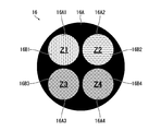
- FIG. 2 is a front view of the bandpass filter unit.
- the bandpass filter unit 16 is composed of a frame body 16A having four opening areas 16A1 to 16A4, and four bandpass filters 16B1 to 16B4 provided in each opening area 16A1 to 16A4 of the frame body 16A.
- the opening area 16A1 is the first opening area 16A1
- the opening area 16A2 is the second opening area 16A2
- the opening area 16A3 is the third opening area 16A3
- the opening area 16A4 is the fourth opening area 16A4.
- Each opening region 16A1 to 16A4 is distinguished by the name.
- the bandpass filter 16B1 provided in the first opening region 16A1 is provided in the first bandpass filter 16B1
- the bandpass filter 16B2 provided in the second opening region 16A2 is provided in the second bandpass filter 16B2 and the third opening region 16A3.
- the bandpass filter 16B3 is referred to as a third bandpass filter 16B3
- the bandpass filter 16B4 provided in the fourth opening region 16A4 is referred to as a fourth bandpass filter 16B4, and the bandpass filters 16B1 to 16B4 are distinguished.
- the frame body 16A has an annular frame body 16a and a partition 16b that partitions the inside of the frame body 16a.
- the frame body 16A is divided into four equal parts in the circumferential direction by a cross-shaped partition 16b inside the frame body 16a, and four opening regions 16A1 to 16A4 are provided.
- the frame body 16a constitutes the diaphragm (aperture diaphragm) of the imaging optical system 10.
- the pupil region is divided into four regions Z1 to Z4 by the frame body 16A (pupil division).
- each of the divided regions Z1 to Z4 will be referred to as a first pupil region Z1, a second pupil region Z2, a third pupil region Z3, and a fourth pupil region Z4, respectively, as necessary.
- the aperture regions 16A1 to 16A4 correspond to the four pupil regions Z1 to Z4 of the imaging optical system 10. That is, the first aperture region 16A1 corresponds to the first pupil region Z1.
- the second aperture region 16A2 corresponds to the second pupil region Z2.
- the third aperture region 16A3 corresponds to the third pupil region Z3.
- the fourth aperture region 16A4 corresponds to the fourth pupil region Z4.
- the wavelength band of light passing through is limited by the bandpass filters 16B1 to 16B4 provided in each aperture region 16A1 to 16A4. That is, in the first pupil region Z1, the wavelength band of the passing light is limited by the first bandpass filter 16B1. In the second pupil region Z2, the wavelength band of light passing through is limited by the second bandpass filter 16B2. In the third pupil region Z3, the wavelength band of light passing through is limited by the third bandpass filter 16B3. In the fourth pupil region Z4, the wavelength band of light passing through is limited by the fourth bandpass filter 16B4.
- the bandpass filters 16B1 to 16B4 are examples of optical elements.
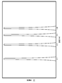
- FIG. 3 is a graph showing an example of the transmission wavelength characteristics of each bandpass filter.
- Each bandpass filter 16B1 to 16B4 transmits light in a different wavelength band. Specifically, the first bandpass filter 16B1 transmits light in the wavelength band ⁇ 1. The second bandpass filter 16B2 transmits light in the wavelength band ⁇ 2. The third bandpass filter 16B3 transmits light in the wavelength band ⁇ 3. The fourth bandpass filter 16B4 transmits light in the wavelength band ⁇ 4.
- each bandpass filter 16B1 to 16B4 has a function of individually correcting the aberration of the region corresponding to each pupil region Z1 to Z4. This point will be described in detail later.
- the imaging optical system 10 has different wavelengths of light passing through the regions corresponding to the pupil regions Z1 to Z4.
- FIG. 4 is a front view of the polarizing filter unit.
- the polarizing filter unit 18 is composed of a frame body 18A having four opening regions 18A1 and 18A2, and four polarizing filters 18B1 to 18B4 provided in each opening regions 18A1 to 18A4 of the frame body 18A.
- the opening area 18A1 is the first opening area 18A1
- the opening area 18A2 is the second opening area 18A2
- the opening area 18A3 is the third opening area 18A3
- the opening area 18A4 is the fourth opening area 18A4.
- the polarizing filter 18B1 provided in the first opening region 18A1 is used as the first polarizing filter 18B1
- the polarizing filter 18B2 provided in the second opening region 18A2 is used as the second polarizing filter 18B2
- the polarizing filter 18B3 provided in the third opening region 18A3 is used.
- the polarizing filters 18B4 provided in the third polarizing filter 18B3 and the fourth aperture region 18A4 are referred to as the fourth polarizing filter 18B4, and the polarizing filters 18B1 to 18B4 are distinguished from each other.
- the frame body 18A has the same shape as the frame body 16A of the bandpass filter unit 16. Therefore, it has an annular frame body 18a and a partition 18b.
- the frame body 18A is provided with four opening regions 18A1 to 18A4 by dividing the inner peripheral portion of the frame body 18a into four equal parts in the circumferential direction by a cross-shaped partition 18b.
- the opening regions 18A1 to 18A4 are arranged so as to overlap the opening regions 16A1 to 16A4 of the bandpass filter unit 16. That is, the first opening region 18A1 is arranged so as to overlap the first opening region 16A1 of the bandpass filter unit 16.
- the second opening region 18A2 is arranged so as to overlap the second opening region 16A2 of the bandpass filter unit 16.
- the third opening region 18A3 is arranged so as to overlap the third opening region 16A3 of the bandpass filter unit 16.
- the fourth opening region 18A4 is arranged so as to overlap the fourth opening region 16A4 of the bandpass filter unit 16. Therefore, the light that has passed through the first aperture region 16A1 of the bandpass filter unit 16 passes through the first aperture region 18A1 of the polarizing filter unit 18. Further, the light that has passed through the second aperture region 16A2 of the bandpass filter unit 16 passes through the second aperture region 18A2 of the polarizing filter unit 18. Further, the light that has passed through the third aperture region 16A3 of the bandpass filter unit 16 passes through the third aperture region 18A3 of the polarizing filter unit 18. Further, the light that has passed through the fourth aperture region 16A4 of the bandpass filter unit 16 passes through the fourth aperture region 18A4 of the polarizing filter unit 18.
- the polarizing filters 18B1 to 18B4 are examples of polarizers.
- light having different characteristics is emitted from the regions corresponding to the pupil regions Z1 to Z4. That is, light having a polarization direction ⁇ 1 and a wavelength band ⁇ 1 (first light), light having a polarization direction ⁇ 2 and a wavelength band ⁇ 2 (second light), light having a polarization direction ⁇ 3 and a wavelength band ⁇ 3 (third light), Then, (fourth light) having a polarization direction ⁇ 4 and a wavelength band ⁇ 4 is emitted.
- the first light is light that passes through the pupil region Z1 and is light that passes through the first bandpass filter 16B1 and the first polarizing filter 18B1.
- the second light is light that passes through the pupil region Z2, and is light that passes through the second bandpass filter 16B2 and the second polarizing filter 18B2.
- the third light is light that passes through the pupil region Z3, and is light that passes through the third bandpass filter 16B3 and the third polarizing filter 18B3.
- the fourth light is light that passes through the pupil region Z4, and is light that passes through the fourth bandpass filter 16B4 and the fourth polarizing filter 18B4.
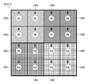
- FIG. 5 is a diagram showing a schematic configuration of an array of pixels of the image sensor.
- the image sensor 100 has a plurality of types of pixels P1 to P16 on its light receiving surface.
- the pixels P1 to P16 are regularly arranged at a constant pitch along the horizontal direction (x-axis direction) and the vertical direction (y-axis direction).
- one pixel block PB (X, Y) is composed of 16 adjacent (4 ⁇ 4) pixels P1 to P16, and the pixel block PB (X, Y) is formed.
- the pixel P1 is the first pixel P1
- the pixel P2 is the second pixel P2
- the pixel P3 is the third pixel P3
- the pixel P4 is the fourth pixel P4
- the pixel P5 is the fifth pixel P5, and the pixel P6.
- the sixth pixel P6, the pixel P7 is the seventh pixel P7, the pixel P8 is the eighth pixel P8, the pixel P9 is the ninth pixel P9, the pixel P10 is the tenth pixel P10, the pixel P11 is the eleventh pixel P11, and the pixel P12 is the twelfth.
- Pixels P12 and P13 are the 13th pixel P13, the pixel P14 is the 14th pixel P14, the pixel P15 is the 15th pixel P15, and the pixel P16 is the 16th pixel P16, and each pixel P1 to P16 is distinguished. Each pixel P1 to P16 has different optical characteristics.
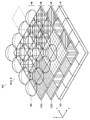
- FIG. 6 is a diagram showing a schematic configuration of an image sensor. Further, FIG. 7 is a cross-sectional view showing a schematic configuration of one pixel (broken line portion in FIG. 6).
- the image pickup device 100 includes a pixel array layer 110, a polarizing filter element array layer 120, a spectroscopic filter element array layer 130, and a microlens array layer 140. Each layer is arranged in the order of the pixel array layer 110, the polarizing filter element array layer 120, the spectroscopic filter element array layer 130, and the microlens array layer 140 from the image plane side to the object side.
- the pixel array layer 110 is configured by arranging a large number of photodiodes 112 two-dimensionally.
- One photodiode 112 constitutes one pixel.
- Each photodiode 112 is regularly arranged along the horizontal direction (x direction) and the vertical direction (y direction).
- the polarizing filter element array layer 120 is configured by two-dimensionally arranging four types of polarizing filter elements 122A to 122D having different polarization directions of the transmitted light.
- the polarizing filter element 122A is the first polarizing filter element 122A
- the polarizing filter element 122B is the second polarizing filter element 122B
- the polarizing filter element 122C is the third polarizing filter element 122C
- the polarizing filter element 122D is the fourth.
- each polarizing filter element 122A to 122D is distinguished.
- the polarizing filter elements 122A to 122D are arranged at the same intervals as the photodiode 112, and are provided for each pixel. In each pixel block PB (X, Y), each polarizing filter element 122A to 122D is regularly arranged.
- FIG. 8 is a diagram showing an example of an arrangement pattern of polarizing filter elements in one pixel block.
- the first polarizing filter element 122A is provided in the first pixel P1, the third pixel P3, the ninth pixel P9, and the eleventh pixel P11.
- a second polarizing filter element 122B is provided in the second pixel P2, the fourth pixel P4, the tenth pixel P10, and the twelfth pixel P12.
- the third pixel P3, the seventh pixel P7, the thirteenth pixel P13, and the fifteenth pixel P15 are provided with the third polarizing filter element 122C.
- the 4th pixel P4, the 8th pixel P8, the 14th pixel P14, and the 16th pixel P16 are provided with the fourth polarizing filter element 122D.
- the spectroscopic filter element array layer 130 is configured by two-dimensionally arranging four types of spectroscopic filter elements 132A to 132D having different transmission wavelength characteristics.
- the spectroscopic filter element 132A is the first spectroscopic filter element 132A
- the spectroscopic filter element 132B is the second spectroscopic filter element 132B
- the spectroscopic filter element 132C is the third spectroscopic filter element 132C
- the spectroscopic filter element 132D is the fourth.
- each spectroscopic filter element 132A to 132D is distinguished.
- the spectroscopic filter elements 132A to 132D are arranged at the same intervals as the photodiode 112, and are provided for each pixel. In each pixel block PB (X, Y), the spectroscopic filter elements 132A to 132D are regularly arranged.
- FIG. 9 is a diagram showing an example of an arrangement pattern of spectral filter elements in one pixel block.
- the first spectral filter element 132A is provided in the first pixel P1, the second pixel P2, the fifth pixel P5, and the sixth pixel P6.
- the second spectral filter element 132B is provided in the third pixel P3, the fourth pixel P4, the seventh pixel P7, and the eighth pixel P8.
- the ninth pixel P9, the tenth pixel P10, the thirteenth pixel P13, and the fourteenth pixel P14 are provided with the third spectral filter element 132C.
- the 11th pixel P11, the 12th pixel P12, the 15th pixel P15, and the 16th pixel P16 are provided with the fourth spectral filter element 132D.
- FIG. 10 is a graph showing an example of transmission wavelength characteristics of each spectroscopic filter element.
- A indicates the transmission wavelength characteristic of the first spectral filter element 132A.
- B shows the transmission wavelength characteristic of the second spectral filter element 132B.
- C indicates the transmission wavelength characteristic of the third spectral filter element 132C.
- D indicates the transmission wavelength characteristic of the fourth spectral filter element 132D.
- the spectroscopic filter elements 132A to 132D have different transmission wavelength characteristics.
- the first spectroscopic filter element 132A is composed of a spectroscopic filter element that transmits blue (Blue, B) light
- the second spectroscopic filter element 132B transmits green (Green, G) light
- the third spectroscopic filter element 132C is composed of a spectroscopic filter element that transmits red (Red, R) light
- the fourth spectroscopic filter element 132D is composed of infrared light (Infrared, IR).
- An example is shown in the case of being composed of a spectroscopic filter element for transmitting infrared rays.
- the wavelength bands ⁇ 1 to ⁇ 4 of the light transmitted by the bandpass filters 16B1 to 16B4 of the imaging optical system 10 are within the wavelength band transmitted by the spectral filter elements 132A to 132D.
- the wavelength bands ⁇ 1 to ⁇ 4 of the light transmitted by the bandpass filters 16B1 to 16B4 are set in the region where the wavelength bands transmitted by the spectral filter elements 132A to 132D overlap.
- the transmission wavelength bands of the spectroscopic filter elements 132A to 132D are set so as to cover the transmission wavelength bands of the bandpass filters 16B1 to 16B4 of the imaging optical system 10. Therefore, each spectroscopic filter element 132A to 132D uses a filter that transmits light in a wide band.
- the microlens array layer 140 is configured by arranging a large number of microlenses 142 two-dimensionally. Each microlens 142 is arranged at the same spacing as the photodiode 112 and is provided for each pixel. The microlens 142 is provided for the purpose of efficiently condensing the light from the imaging optical system 10 on the photodiode 112.
- each pixel P1 to P16 receives light from the image pickup optical system 10 as follows. That is, the first pixel P1 receives light from the imaging optical system 10 via the first spectral filter element 132A (transmission wavelength characteristic A) and the first polarizing filter element 122A (polarization direction ⁇ A). Further, the second pixel P2 receives light from the imaging optical system 10 via the first spectral filter element 132A (transmission wavelength characteristic A) and the second polarizing filter element 122B (polarization direction ⁇ B).
- the third pixel P3 receives light from the imaging optical system 10 via the second spectral filter element 132B (transmission wavelength characteristic B) and the first polarizing filter element 122A (polarization direction ⁇ A). Further, the fourth pixel P4 receives light from the imaging optical system 10 via the second spectral filter element 132B (transmission wavelength characteristic B) and the second polarizing filter element 122B (polarization direction ⁇ B). Further, the fifth pixel P5 receives light from the imaging optical system 10 via the first spectral filter element 132A (transmission wavelength characteristic A) and the third polarizing filter element 122C (polarization direction ⁇ C).
- the sixth pixel P6 receives light from the imaging optical system 10 via the first spectral filter element 132A (transmission wavelength characteristic A) and the fourth polarizing filter element 122D (polarization direction ⁇ D). Further, the seventh pixel P7 receives light from the imaging optical system 10 via the second spectral filter element 132B (transmission wavelength characteristic B) and the third polarizing filter element 122C (polarization direction ⁇ C). Further, the eighth pixel P8 receives light from the imaging optical system 10 via the second spectral filter element 132B (transmission wavelength characteristic B) and the fourth polarizing filter element 122D (polarization direction ⁇ D).
- the ninth pixel P9 receives light from the imaging optical system 10 via the third spectral filter element 132C (transmission wavelength characteristic C) and the first polarizing filter element 122A (polarization direction ⁇ A). Further, the tenth pixel P10 receives light from the imaging optical system 10 via the third spectral filter element 132C (transmission wavelength characteristic C) and the second polarizing filter element 122B (polarization direction ⁇ B). Further, the 11th pixel P11 receives light from the imaging optical system 10 via the fourth spectral filter element 132D (transmission wavelength characteristic D) and the first polarizing filter element 122A (polarization direction ⁇ A).
- the 12th pixel P12 receives light from the imaging optical system 10 via the fourth spectral filter element 132D (transmission wavelength characteristic D) and the second polarization filter element 122B (polarization direction ⁇ B). Further, the 13th pixel P13 receives light from the imaging optical system 10 via the third spectral filter element 132C (transmission wavelength characteristic C) and the third polarizing filter element 122C (polarization direction ⁇ C). Further, the 14th pixel P14 receives light from the imaging optical system 10 via the third spectral filter element 132C (transmission wavelength characteristic C) and the fourth polarizing filter element 122D (polarization direction ⁇ D).
- the 15th pixel P15 receives light from the imaging optical system 10 via the fourth spectral filter element 132D (transmission wavelength characteristic D) and the third polarizing filter element 122C (polarization direction ⁇ C). Further, the 16th pixel P16 receives light from the imaging optical system 10 via the fourth spectral filter element 132D (transmission wavelength characteristic D) and the fourth polarizing filter element 122D (polarization direction ⁇ D). As described above, each of the pixels P1 to P16 receives light having different characteristics by having different optical characteristics from each other. That is, it receives light having different wavelength bands and polarization directions.
- the signal processing unit 200 processes the signal output from the image sensor 100 to generate image data of a 4-band multispectral image. That is, image data of four types of wavelength bands ⁇ 1 to ⁇ 4 that pass through the bandpass filter unit 16 of the imaging optical system 10 are generated.
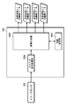
- FIG. 11 is a block diagram showing a schematic configuration of a signal processing unit.
- the signal processing unit 200 includes an analog signal processing unit 200A, an image generation unit 200B, and a coefficient storage unit 200C.
- the analog signal processing unit 200A takes in the analog pixel signal output from each pixel of the image pickup element 100, performs predetermined signal processing (for example, correlation double sampling processing, amplification processing, etc.), and then converts it into a digital signal. And output.
- predetermined signal processing for example, correlation double sampling processing, amplification processing, etc.
- the image generation unit 200B performs predetermined signal processing on the pixel signal after being converted into a digital signal, and generates image data in each wavelength band ⁇ 1 to ⁇ 4.
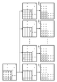
- FIG. 12 is a conceptual diagram of image generation.
- Each pixel block PB (X, Y) includes 16 pixels P1 to P16. Therefore, 16 image data D1 to D16 are generated by separating and extracting the pixel signals of the pixels P1 to P16 from the pixel blocks PB (X, Y). However, interference (crosstalk) has occurred in the 16 image data D1 to D16. That is, since light in each wavelength band is incident on each pixel P1 to P16, the generated image is an image in which images in each wavelength band are mixed at a predetermined ratio. Therefore, the image generation unit 200B performs the interference removal process to generate image data in each wavelength band.
- the pixel signal (signal value) obtained from the first pixel P1 of each pixel block PB (X, Y) is ⁇ 1
- the pixel signal obtained from the second pixel P2 is ⁇ 2
- the pixel signal obtained from the third pixel P3 is ⁇ 3.
- the pixel signal obtained by the 4th pixel P4 is ⁇ 4, the pixel signal (signal value) obtained by the 5th pixel P5 is ⁇ 5, the pixel signal obtained by the 6th pixel P6 is ⁇ 6, and the pixel signal obtained by the 7th pixel P7 is ⁇ 7, the pixel signal obtained by the eighth pixel P8 is ⁇ 8, the pixel signal (signal value) obtained by the ninth pixel P9 is ⁇ 9, the pixel signal (signal value) obtained by the first pixel P1 is ⁇ 1, and the second pixel P2.
- the pixel signal obtained in the above is ⁇ 2, the pixel signal obtained in the third pixel P3 is ⁇ 3, the pixel signal obtained in the fourth pixel P4 is ⁇ 4, and the pixel signal (signal value) obtained in the tenth element P10 is ⁇ 10, eleventh.
- the pixel signal (signal value) obtained by the pixel P11 is ⁇ 11
- the pixel signal obtained by the 12th pixel P12 is ⁇ 12
- the pixel signal obtained by the 13th pixel P13 is ⁇ 13
- the pixel signal obtained by the 14th pixel P14 is ⁇ 14.
- the pixel signal (signal value) obtained by the 15th pixel P15 is ⁇ 15
- the pixel signal obtained by the 16th pixel P16 is ⁇ 16.
- 16 pixel signals ⁇ 1 to ⁇ 16 can be obtained.
- the image generation unit 200B calculates four pixel signals ⁇ 1 to ⁇ 4 corresponding to light in each wavelength band ⁇ 1 to ⁇ 4 from the 16 pixel signals ⁇ 1 to ⁇ 16, and removes interference. Specifically, four pixel signals ⁇ 1 to ⁇ 4 corresponding to light in each wavelength band ⁇ 1 to ⁇ 4 are calculated by Equation 1 using the following matrix A, and interference is eliminated.
- the pixel signal ⁇ 1 is a pixel signal corresponding to light in the wavelength band ⁇ 1
- the pixel signal ⁇ 2 is a pixel signal corresponding to light in the wavelength band ⁇ 2
- the pixel signal ⁇ 3 is a pixel signal corresponding to light in the wavelength band ⁇ 3, and the pixel signal ⁇ 4.
- the reason why the interference can be eliminated by the above equation 1 will be described.
- Interference occurs when light in each wavelength band ⁇ 1 to ⁇ 4 is mixed into each pixel P1 to P16.
- b11 is the ratio of light in the wavelength band ⁇ 1 received by the first pixel P1
- b12 is the ratio of light in the wavelength band ⁇ 2 received by the first pixel P1
- b13 is the ratio of light in the wavelength band ⁇ 3.
- the ratio of light received by the first pixel P1, b14 is the ratio of light in the wavelength band ⁇ 4 received by the first pixel P1.
- b21 is the ratio of light in the wavelength band ⁇ 1 received by the second pixel P2
- b22 is the ratio of light received in the wavelength band ⁇ 2 by the second pixel P2
- b23 is the ratio of light in the wavelength band ⁇ 3.
- the ratio of light received by the two pixels P2, b24 is the ratio of light received in the wavelength band ⁇ 4 received by the second pixel P2.
- b31 is the ratio of light in the wavelength band ⁇ 1 received by the third pixel P3
- b32 is the ratio of light received in the wavelength band ⁇ 2 by the third pixel P3,
- b33 is the ratio of light in the wavelength band ⁇ 3.
- the ratio of light received by the three pixels P3, b34 is the ratio of light received in the wavelength band ⁇ 4 received by the third pixel P3. Further, b41 is the ratio of light in the wavelength band ⁇ 1 received by the fourth pixel P4, b42 is the ratio of light received in the wavelength band ⁇ 2 by the fourth pixel P4, and b43 is the ratio of light in the wavelength band ⁇ 3. The ratio of light received by the four pixels P4, b44, is the ratio of light received in the wavelength band ⁇ 4 received by the fourth pixel P4.
- b51 is the ratio of light in the wavelength band ⁇ 1 received by the fifth pixel P5
- b52 is the ratio of light received in the wavelength band ⁇ 2 by the fifth pixel P5
- b53 is the ratio of light in the wavelength band ⁇ 3.
- the ratio of light received by the 5th pixel P5, b54 is the ratio of light received in the wavelength band ⁇ 4 being received by the 5th pixel P5.
- b61 is the ratio of light in the wavelength band ⁇ 1 received by the sixth pixel P6, b62 is the ratio of light in the wavelength band ⁇ 2 received by the sixth pixel P6, and b63 is the ratio of light in the wavelength band ⁇ 3.
- the ratio of light received by the 6-pixel P6, b64 is the ratio of the light in the wavelength band ⁇ 4 received by the 6-pixel P6.
- b71 is the ratio of light in the wavelength band ⁇ 1 received by the seventh pixel P7
- b72 is the ratio of light in the wavelength band ⁇ 2 received by the seventh pixel P7
- b73 is the ratio of light in the wavelength band ⁇ 3.
- the ratio of light received by the 7-pixel P7, b74 is the ratio of the light in the wavelength band ⁇ 4 received by the 7th pixel P7.
- b81 is the ratio of light in the wavelength band ⁇ 1 received by the eighth pixel P8
- b82 is the ratio of light received in the wavelength band ⁇ 2 by the eighth pixel P8
- b83 is the ratio of light in the wavelength band ⁇ 3.
- the ratio of light received by the eight pixels P8, b84 is the ratio of light received in the wavelength band ⁇ 4 being received by the eighth pixel P8.
- b91 is the ratio of light in the wavelength band ⁇ 1 received by the ninth pixel P9
- b92 is the ratio of light received in the wavelength band ⁇ 2 in the ninth pixel P9
- b93 is the ratio of light in the wavelength band ⁇ 3.
- the ratio of light received by the 9-pixel P9, b94 is the ratio of the light in the wavelength band ⁇ 4 received by the 9th pixel P9.
- b101 is the ratio of light in the wavelength band ⁇ 1 received by the 10th pixel P10
- b102 is the ratio of light received in the wavelength band ⁇ 2 in the 10th pixel P10
- b103 is the ratio of light in the wavelength band ⁇ 3.
- the ratio of light received by the 10 pixels P10, b104 is the ratio of light received in the wavelength band ⁇ 4 received by the 10th pixel P10.
- b111 is the ratio of light in the wavelength band ⁇ 1 received by the 11th pixel P11
- b112 is the ratio of light in the wavelength band ⁇ 2 received by the 11th pixel P11
- b113 is the ratio of light in the wavelength band ⁇ 3.
- the ratio of light received by the 11th pixel P11, b114, is the ratio of light received in the wavelength band ⁇ 4 being received by the 11th pixel P11.
- b121 is the ratio of light in the wavelength band ⁇ 1 received by the 12th pixel P12
- b122 is the ratio of light received in the wavelength band ⁇ 2 in the 12th pixel P12
- b123 is the ratio of light in the wavelength band ⁇ 3.
- the ratio of light received by the 12-pixel P12, b124 is the ratio of the light in the wavelength band ⁇ 4 received by the 12-pixel P12. Further, b131 is the ratio of light in the wavelength band ⁇ 1 received by the 13th pixel P13, b132 is the ratio of light received in the wavelength band ⁇ 2 by the 13th pixel P13, and b133 is the ratio of light in the wavelength band ⁇ 3.
- the ratio of light received by the 13-pixel P13, b134 is the ratio of the light in the wavelength band ⁇ 4 received by the 13-pixel P13.
- b141 is the ratio of light in the wavelength band ⁇ 1 received by the 14th pixel P14
- b142 is the ratio of light received in the wavelength band ⁇ 2 in the 14th pixel P14
- b143 is the ratio of light in the wavelength band ⁇ 3.
- the ratio of light received by the 14-pixel P14, b144, is the ratio of light in the wavelength band ⁇ 4 received by the 14-pixel P14.
- b151 is the ratio of light in the wavelength band ⁇ 1 received in the 15th pixel P15
- b152 is the ratio of light in the wavelength band ⁇ 2 received in the 15th pixel P15
- b153 is the ratio of light in the wavelength band ⁇ 3.
- the ratio of light received by the 15 pixels P15, b154, is the ratio of light received in the wavelength band ⁇ 4 received by the 15th pixel P15.
- b161 is the ratio of light in the wavelength band ⁇ 1 received by the 16th pixel P16
- b162 is the ratio of light received in the wavelength band ⁇ 2 in the 16th pixel P16
- b163 is the ratio of light in the wavelength band ⁇ 3.
- the ratio of light received by the 16-pixel P16, b164, is the ratio of light in the wavelength band ⁇ 4 received by the 16th pixel P16.
- This ratio bij sets the wavelength bands ⁇ 1 to ⁇ 4 of the light transmitted by the opening regions 16A1 to 16A4 of the bandpass filter unit 16, and the polarization direction ⁇ 1 of the light transmitted by the opening regions 18A1 to 18A4 of the polarizing filter unit 18. It is uniquely determined from the setting of ⁇ 2, the transmission wavelength characteristics A to D of the pixels P1 to P16 of the image pickup element 100, and the polarization directions ⁇ A to ⁇ C of the light received by the pixels P1 to P16 of the image pickup element 100. Can be asked for.
- the following relationship is between the pixel signals ⁇ 1 to ⁇ 16 obtained from the pixels P1 to P16 of each pixel block PB (X, Y) and the pixel signals ⁇ 1 to ⁇ 4 corresponding to the light of each wavelength band ⁇ 1 to ⁇ 4. Holds.
- ⁇ 1 to ⁇ 4 which are the solutions of the simultaneous equations of equations 2 to 17, are calculated by multiplying both sides of the above equation 18 by the inverse matrix B -1 of the matrix B.
- the light of the respective wavelength bands ⁇ 1 to ⁇ 4 emitted from the imaging optical system 10 is the light of each pixel P1 of the pixel block PB (X, Y). It can be calculated from the signal values (pixel signals) ⁇ 1 to ⁇ 16 of each pixel P1 to P16 based on the ratio of light received by ⁇ P16.
- the coefficient storage unit 200C stores each element aij of the matrix A for performing the interference removal process as a coefficient group.
- the image generation unit 200B acquires a coefficient group from the coefficient storage unit 200C, and from the pixel signals ⁇ 1 to ⁇ 16 obtained from the pixels P1 to P16 of each pixel block PB (X, Y), each wavelength band is obtained by the above equation 1. Pixel signals ⁇ 1 to ⁇ 4 corresponding to ⁇ 1 to ⁇ 4 are calculated, and image data of each wavelength band ⁇ 1 to ⁇ 4 is generated.
- the image data of each wavelength band ⁇ 1 to ⁇ 4 generated by the image generation unit 200B is output to the outside and stored in a storage device (not shown) as needed. In addition, it is displayed on a display (not shown) as needed.
- FIG. 13 is a conceptual diagram of image generation by the imaging device.
- the light incident on the image pickup optical system 10 becomes four types of light having different characteristics and is incident on the image pickup element 100. Specifically, light having a polarization direction ⁇ 1 and a wavelength band ⁇ 1 (first light), light having a polarization direction ⁇ 1 and a wavelength band ⁇ 2 (second light), and light having a polarization direction ⁇ 2 and a wavelength band ⁇ 3 (third light). Light) and (fourth light) having a polarization direction ⁇ 2 and a wavelength band ⁇ 4 are incident on the image pickup element 100.
- each pixel block PB (X, Y) of the image sensor 100 light in each wavelength band emitted from the image pickup optical system 10 is received in each pixel P1 to P16 at a predetermined ratio bij. That is, due to the action of the polarizing filter elements 122A to 122D and the spectroscopic filter elements 132A to 132D provided in the pixels P1 to P16, the light in each wavelength band ⁇ 1 to ⁇ 4 is received at a predetermined ratio bij.
- the signal processing unit 200 has pixel signals ⁇ 1 to ⁇ 4 corresponding to light in each wavelength band ⁇ 1 to ⁇ 4 from pixel signals ⁇ 1 to ⁇ 16 obtained from pixels P1 to P16 of each pixel block PB (X, Y) of the image sensor 100. Is calculated, and image data of each wavelength band ⁇ 1 to ⁇ 4 is generated. That is, arithmetic processing (interference removal processing) according to Equation 1 using the matrix A is performed to correspond to light in each wavelength band ⁇ 1 to ⁇ 4 from the pixel signals ⁇ 1 to ⁇ 16 of the pixels P1 to P16 obtained from the image sensor 100. The pixel signals ⁇ 1 to ⁇ 4 are calculated, and image data of each wavelength band ⁇ 1 to ⁇ 4 is generated.
- one image pickup optical system 10 and one (single plate) image pickup element 100 capture images of four different wavelength bands (four-band multispectral images). it can.
- the imaging apparatus 1 of the present embodiment captures a multispectral image by dividing the pupil region of the imaging optical system 10 into a plurality of regions (pupil division) and limiting the wavelength region in each region. Is possible.
- the "general imaging optical system” here means an imaging optical system in which aberrations for each wavelength are not particularly corrected, that is, an imaging optical system in which aberrations for each wavelength remain.
- the bandpass filters 16B1 to 16B4 have a function of individually correcting the aberrations in the regions corresponding to the pupil regions Z1 to Z4.
- each bandpass filter 16B1 to 16B4 has a lens shape having a curvature on at least one surface on the object side and the image side, and the curvature is individually adjusted to cause aberration in the corresponding region. It is corrected individually. That is, by giving the bandpass filter a lens function, the optical path lengths of the regions corresponding to the pupil regions Z1 to Z4 are individually adjusted to correct the aberration.
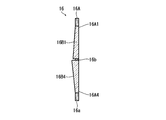
- FIG. 14 is a 14-14 cross-sectional view of the bandpass filter unit shown in FIG.
- the figure shows a cross section of the first bandpass filter 16B1 and the fourth bandpass filter 16B4.
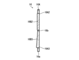
- 15 is a 15-15 cross-sectional view of the bandpass filter unit shown in FIG. 2.
- FIG. The figure shows the cross section of the second bandpass filter 16B2 and the third bandpass filter 16B3.
- each of the bandpass filters 16B1 to 16B4 has a curved surface on one side (the surface on the object side (left side in FIGS. 14 and 15)).
- the curvature of one side of the bandpass filters 16B1 to 16B4 is individually adjusted, and the aberration of the region corresponding to each pupil region Z1 to Z4 is corrected.
- the aberration of the region corresponding to the first pupil region Z1 is corrected by adjusting the curvature of one side of the first bandpass filter 16B1.
- the aberration is corrected by adjusting the curvature of one side of the second bandpass filter 16B2.
- the aberration is corrected by adjusting the curvature of one side of the third bandpass filter 16B3. Further, for the region corresponding to the fourth pupil region Z4, the aberration is corrected by adjusting the curvature of the surface of the fourth bandpass filter 16B4 on the object side.
- each bandpass filter 16B1 to 16B4 changes by changing the curvature of one side. Let the focal lengths at the center wavelength of the light passing through the pupil regions Z1 to Z4 of the imaging optical system 10 be f1, f2, f3, and f4. The focal lengths of the bandpass filters 16B1 to 16B4 are shortened in descending order of the focal lengths f1, f2, f3, and f4.
- the imaging optical system 10 the aberrations in the regions corresponding to the pupil regions Z1 to Z4 are individually corrected by the bandpass filters 16B1 to 16B4. As a result, the imaging optical system 10 has different aberration characteristics in the regions corresponding to the pupil regions Z1 to Z4.
- the aberrations in the regions corresponding to the pupil regions Z1 to Z4 can be individually controlled, so that the aberrations can be controlled for each wavelength. This makes it possible to capture a multispectral image with good image quality.
- the method of this embodiment can also be applied to an existing imaging lens (general imaging lens not for multispectral imaging). That is, since the method of the present embodiment only arranges a bandpass filter in each pupil-divided region and adjusts the curvature of each bandpass filter, it can be applied to an existing imaging lens. Therefore, by using the method of the present embodiment, the existing imaging lens can be used as an imaging lens for multispectral imaging.
- an existing imaging lens generally imaging lens not for multispectral imaging. That is, since the method of the present embodiment only arranges a bandpass filter in each pupil-divided region and adjusts the curvature of each bandpass filter, it can be applied to an existing imaging lens. Therefore, by using the method of the present embodiment, the existing imaging lens can be used as an imaging lens for multispectral imaging.
- each bandpass filter 16B1 to 16B4 has a curvature on only one side, but both sides may have a curvature.
- the imaging optical system has a configuration in which the wavelengths of light passing through each pupil region are different from each other and the aberration characteristics of the regions corresponding to each pupil region are different from each other.
- the bandpass filters 16B1 to 16B4 provided in the regions corresponding to the pupil regions Z1 to Z4 limit the wavelength band of light passing through the regions corresponding to the pupil regions Z1 to Z4.
- the bandpass filters 16B1 to 16B4 provided in the regions corresponding to the pupil regions Z1 to Z4 individually correct the aberrations in the regions corresponding to the pupil regions Z1 to Z4, and correspond to the pupil regions Z1 to Z4. It is assumed that the aberration characteristics of the regions to be affected are different from each other. It is the same as the imaging device 1 of the first embodiment, except that the aberration correction method is different. Therefore, here, the aberration correction method by the bandpass filters 16B1 to 16B4 will be described.
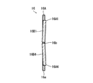
- FIG. 16 is a diagram showing the configuration of the bandpass filter unit of the present embodiment.
- (A) shows a side view of the bandpass filter unit
- (B) shows a front view of the bandpass filter unit.
- FIG. 17 is a cross-sectional view taken along the line 17-17 of FIG.
- the figure shows a cross section of the first bandpass filter 16B1 and the fourth bandpass filter 16B4.
- 18 is a cross-sectional view taken along the line 18-18 of FIG.
- the figure shows the cross section of the second bandpass filter 16B2 and the third bandpass filter 16B3.
- the bandpass filters 16B1 to 16B4 of the present embodiment have a flat plate shape.
- the imaging optical system 10 is formed by individually adjusting the thicknesses t1 to t4 of the bandpass filters 16B1 to B4 (thicknesses in the direction parallel to the optical axis L) to cover the regions corresponding to the pupil regions Z1 to Z4. Aberrations are corrected individually. That is, due to the difference in thickness t1 to t4, even if the object distance is the same for the entire imaging optical system 10, the object distance for the rear group changes, and the position of the final image plane changes for each wavelength band. Can be done.
- the axial chromatic aberration (deviation of the imaging position for each color) of the imaging optical system 10 is corrected individually for each wavelength band by changing the thicknesses t1 to t4 of the bandpass filters 16B1 to 16B4. it can.
- the focal lengths at the center wavelengths of the light passing through the pupil regions Z1 to Z4 of the imaging optical system 10 are f1, f2, f3, and f4
- each band path is in ascending order of focal lengths f1, f2, f3, and f4.
- the thicknesses t1 to t4 of the filters 16B1 to 16B4 are increased.
- the aberration of the region corresponding to each pupil region Z1 to Z4 can be individually controlled, so that the aberration can be controlled for each wavelength. This makes it possible to capture a multispectral image with good image quality. Further, since the method of the present embodiment can also be applied to an existing imaging lens, the existing imaging lens can be used as an imaging lens for multispectral imaging.
- the imaging optical system has a configuration in which the wavelengths of light passing through each pupil region are different from each other and the aberration characteristics of the regions corresponding to each pupil region are different from each other.
- the bandpass filters 16B1 to 16B4 provided in the regions corresponding to the pupil regions Z1 to Z4 limit the wavelength band of light passing through the regions corresponding to the pupil regions Z1 to Z4.
- the bandpass filters 16B1 to 16B4 provided in the regions corresponding to the pupil regions Z1 to Z4 individually correct the aberrations in the regions corresponding to the pupil regions Z1 to Z4, and correspond to the pupil regions Z1 to Z4. It is assumed that the aberration characteristics of the regions to be affected are different from each other. It is the same as the imaging device 1 of the first embodiment, except that the aberration correction method is different. Therefore, here, the aberration correction method by the bandpass filters 16B1 to 16B4 will be described.
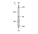
- FIG. 19 is a diagram showing the configuration of the bandpass filter unit of the present embodiment.
- (A) shows a side view of the bandpass filter unit
- (B) shows a front view of the bandpass filter unit.
- FIG. 20 is a cross-sectional view taken along the line 20-20 of FIG.
- the figure shows a cross section of the first bandpass filter 16B1 and the fourth bandpass filter 16B4.
- 21 is a cross-sectional view taken along the line 21-21 of FIG.
- the figure shows the cross section of the second bandpass filter 16B2 and the third bandpass filter 16B3.
- the bandpass filters 16B1 to 16B4 of the present embodiment have a flat plate shape.
- the imaging optical system 10 individually adjusts the inclinations of the bandpass filters 16B1 to B4 to individually correct the aberrations in the regions corresponding to the pupil regions Z1 to Z4.
- FIG. 22 is a diagram schematically showing how the imaging position shifts due to asymmetric pupil division in a lens in which coma aberration remains.
- the position p1 indicates the image formation position when the pupil is not divided
- the position p2 indicates the image formation position when the pupil is divided.
- the central imaging position can be shifted by dividing the pupil in a state where coma is generated at the central imaging point.
- axial chromatic aberration can be suppressed for each wavelength band passing through the respective pupil regions Z1 to Z4. That is, since the imaging position can be changed for each wavelength band, the axial chromatic aberration inherent in the imaging optical system 10 can be canceled for each wavelength band.
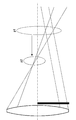
- FIG. 23 is a conceptual diagram of tilt setting.
- the focal length at the d-line (587.6 nm (yellow) emission line spectrum) of the optical system in front of the aperture is f0, and the focal length at the center wavelength of the wavelength band of light passing through the regions corresponding to the respective pupil regions Z1 to Z4. Let it be f1, f2, f3, and f4, respectively.
- ⁇ be the angle with the rotation center of the vector orthogonal to the vector drawn from the center to the center of gravity of the aperture in the aperture plane. The angle ⁇ is positive in the direction of tilting toward the object.
- the angle ⁇ is increased in ascending order of focal lengths f1, f2, f3, and f4.
- the focal length f0 on the d-line of the optical system on the front side of the diaphragm is f ⁇ 0
- the angle ⁇ is increased in descending order of the focal lengths f1, f2, f3, and f4.
- FIG. 24 is a diagram showing another example of the bandpass filter unit of the present embodiment.
- (A) shows a side view of the bandpass filter unit
- (B) shows a front view of the bandpass filter unit.
- FIG. 25 is a cross-sectional view taken along the line 25-25 of FIG. 24.
- the figure shows a cross section of the first bandpass filter 16B1 and the fourth bandpass filter 16B4.
- 26 is a cross-sectional view taken along the line 26-26 of FIG. 24.
- the figure shows the cross section of the second bandpass filter 16B2 and the third bandpass filter 16B3.
- the bandpass filters 16B1 to 16B4 of this example have a flat plate shape with an inclination on one side (the cross section has a wedge shape).
- the imaging optical system 10 individually corrects the aberration in the region corresponding to each pupil region Z1 to Z4.
- the pupil region of the imaging optical system is equally divided in the circumferential direction, but the mode of division of the pupil region is not limited to this.
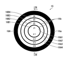
- FIG. 27 is a diagram showing another example (modification example) of the division mode of the pupil region. This figure corresponds to the front view of the bandpass filter unit.
- the pupil region is divided into a plurality of regions by dividing the inner peripheral portion of the frame body 16a constituting the diaphragm into a plurality of regions.
- the inner peripheral portion of the frame body 16a is divided concentrically by a plurality of ring-shaped partitions 16b, and the pupil region of the imaging optical system is divided into a plurality of regions. ..
- FIG. 27 shows an example of the case where the pupil region is divided into four regions.
- the four aperture regions of the frame 16A (first aperture region 16A1, second aperture region 16A2, third aperture region 16A3, fourth aperture region 16A4) each have four pupil regions (first pupil region Z1, second pupil). It corresponds to the area Z2, the third pupil area Z3, and the fourth pupil area Z4). That is, the first aperture region 16A1 corresponds to the first pupil region Z1.
- the second aperture region 16A2 corresponds to the second pupil region Z2.
- the third aperture region 16A3 corresponds to the third pupil region Z3.
- the fourth aperture region 16A4 corresponds to the fourth pupil region Z4.
- the points that the wavelengths of the light passing through the pupil regions Z1 to Z4 are different from each other and the aberration characteristics of the regions corresponding to the pupil regions Z1 to Z4 are different from each other are the same as those of the imaging optical system of the above embodiment. is there. That is, in the imaging optical system, the wavelength band of light passing through the regions corresponding to the pupil regions Z1 to Z4 is limited by the bandpass filters 16B1 to 16B4 provided in the aperture regions 16A1 to 16A4. Further, the bandpass filters 16B1 to 16B4 individually correct the aberrations in the regions corresponding to the pupil regions Z1 to Z4.
- FIG. 28 is a diagram showing an example of a case where the curvature of the bandpass filter is adjusted to correct the aberration. This figure corresponds to the 28-28 cross-sectional view of FIG. 27.
- This example shows an example in which the shape of each bandpass filter 16B1 to 16B4 is set as a lens shape and the aberration of the region corresponding to each pupil region Z1 to Z4 is corrected by individually adjusting the curvature thereof. ..
- only one side (the surface on the object side) of the bandpass filters 16B1 to 16B4 has a curvature, but it is also possible to give a curvature to both sides. Further, the surface on the image side may be configured to have a curvature.
- the wavelength band assigned to each pupil region Z1 to Z4 it is preferable to set the wavelength band assigned to each pupil region Z1 to Z4 according to the required image quality (high image quality is required). Allocate the wavelength band to the central pupil region.
- FIG. 29 is a diagram showing another example of the aberration correction method. The figure shows an example in which the thickness of the bandpass filter is adjusted to correct the aberration.
- each bandpass filter 16B1 to 16B4 is formed into a flat plate shape, and the aberration of the region corresponding to each pupil region Z1 to Z4 is corrected by individually adjusting the thickness thereof.
- FIG. 30 is a diagram showing another example of the aberration correction method. The figure shows an example of a case where the inclination of the bandpass filter is adjusted to correct the aberration.
- each bandpass filter 16B1 to 16B4 is made into a flat plate shape, and the aberration of the region corresponding to each pupil region Z1 to Z4 is corrected by individually adjusting the inclination of one side thereof. ing.
- FIG. 30 shows an example of adjusting the inclination of one side of each bandpass filter
- the inclination of the bandpass filter itself is adjusted to obtain aberrations in the regions corresponding to the pupil regions Z1 to Z4. It can also be configured to be corrected.
- each pupil region Z1 to Z4 it is possible to correct the aberration in the region corresponding to each pupil region Z1 to Z4.
- the curvature of the first bandpass filter is adjusted to correct the aberration
- the thickness of each bandpass filter 16B2 to 16B4 is adjusted. Then, the aberration can be corrected.
- ⁇ Fifth Embodiment When a multispectral image is captured by dividing the pupil region of the imaging optical system, a good dynamic range cannot be obtained if the difference in the amount of light for each wavelength band is large. For example, only an image in a specific wavelength band may be darkened or overexposed.
- the aperture area of each pupil region is adjusted individually, and the amount of light for each wavelength band is adjusted individually.
- the adjustment of the opening area of each pupil region is realized by adjusting the area (opening area) of each opening region of the frame body constituting the bandpass filter unit. It is the same as the imaging device 1 of the first embodiment, except that the aperture area of each pupil region is adjusted by the bandpass filter unit. Therefore, only the configuration of the bandpass filter unit will be described here.
- FIG. 31 is a diagram showing the configuration of the bandpass filter unit of the present embodiment.
- the outer peripheral diameters of the opening regions 16A1 to 16A4 are individually adjusted, and the areas (opening areas) of the opening regions 16A1 to 16A4 are individually adjusted. Is adjusted to.
- the areas of the respective aperture regions 16A1 to 16A4 are individually adjusted, so that the aperture areas of the corresponding pupil regions Z1 to Z4 are individually adjusted.
- the aperture area of each pupil region Z1 to Z4 is individually adjusted, so that the amount of light passing through each pupil region Z1 to Z4 is individually adjusted.
- the amount of light passing through each pupil region Z1 to Z4 is different from each other.
- each pupil region Z1 to Z4 by reducing the opening area of each pupil region Z1 to Z4, it is possible to reduce the aberration of the region corresponding to each pupil region Z1 to Z4. Therefore, by individually adjusting the opening area of each pupil region Z1 to Z4, the aberration of the region corresponding to each pupil region Z1 to Z4 can be individually corrected. For example, the opening area is reduced as the distance from the d line increases. Since a normal image pickup lens is designed with reference to the vicinity of the d line, the aberration increases as the distance from the d line increases. Therefore, it is preferable to reduce the aperture area and reduce the aberration as the wavelength becomes farther from the d line.
- each opening area 16A1 to 16A4 is changed to adjust the area of each opening area 16A1 to 16A4, but the method of adjusting the area of each opening area 16A1 to 16A4. Is not limited to this.
- the area of each opening region 16A1 to 16A4 can be adjusted by changing the width of the partition 16b.
- ⁇ 6th Embodiment As described above, by individually adjusting the amount of light passing through each pupil region Z1 to Z4, the amount of light for each wavelength band can be individually adjusted, and a good dynamic range can be obtained.
- the aperture areas of the pupil regions Z1 to Z4 are individually adjusted, and the amount of light passing through the pupil regions Z1 to Z4 is individually adjusted.
- the transmittance of the bandpass filters 16B1 to 16B4 provided corresponding to the pupil regions Z1 to Z4 is adjusted to adjust the amount of light passing through the pupil regions Z1 to Z4.
- FIG. 32 is a graph showing an example of the transmission wavelength characteristics of each bandpass filter provided in the bandpass filter unit of the present embodiment.
- the first bandpass filter 16B1 transmits light in the wavelength band ⁇ 1.
- the second bandpass filter 16B2 transmits light in the wavelength band ⁇ 2.
- the third bandpass filter 16B3 transmits light in the wavelength band ⁇ 3.
- the fourth bandpass filter 16B4 transmits light in the wavelength band ⁇ 4.
- each bandpass filter 16B1 to 16B4 transmits light in each wavelength band ⁇ 1 to ⁇ 4 with different transmittances.
- the transmittance of the bandpass filters 16B1 to 16B4 provided corresponding to the pupil regions Z1 to Z4 is individually adjusted, and the amount of light passing through the pupil regions Z1 to Z4 is individually adjusted. You can also. As a result, a good dynamic range can be obtained.
- the resolution is also good by controlling the transmittance as in the present embodiment. Image can be obtained.
- the adjustment method of the present embodiment can also be used in combination with the method of adjusting the opening area of each pupil region Z1 to Z4.
- the bandwidth of the light passing through the pupil regions Z1 to Z4 is adjusted to adjust the amount of light passing through the pupil regions Z1 to Z4.
- the bandwidth of the light passing through the pupil regions Z1 to Z4 is adjusted by changing the bandwidth of the wavelength transmitted by the bandpass filters 16B1 to 16B4.
- FIG. 33 is a graph showing an example of the transmission wavelength characteristics of each bandpass filter provided in the bandpass filter unit of the present embodiment.
- the bandpass filters 16B1 to 16B4 have different bandwidths of the wavelength bands ⁇ 1 to ⁇ 4 to be transmitted.
- the amount of light in the first pupil region Z1 is adjusted by adjusting the bandwidth of the wavelength band ⁇ 1 transmitted by the first bandpass filter 16B1.
- the amount of light in the second pupil region Z2 is adjusted by adjusting the bandwidth of the wavelength band ⁇ 2 transmitted by the second bandpass filter 16B2.
- the amount of light in the third pupil region Z3 is adjusted by adjusting the bandwidth of the wavelength band ⁇ 3 transmitted by the third bandpass filter 16B3.
- the amount of light in the fourth pupil region Z4 is adjusted by adjusting the bandwidth of the wavelength band ⁇ 4 transmitted by the fourth bandpass filter 16B4.
- the bandwidth of the wavelength bands ⁇ 1 to ⁇ 4 transmitted by the bandpass filters 16B1 to 16B4 can be individually adjusted, and the amount of light passing through the pupil regions Z1 to Z4 can be individually adjusted. As a result, a good dynamic range can be obtained.
- the adjustment method of the present embodiment is used in combination with a method of adjusting the opening area of each pupil region Z1 to Z4 and / or a method of adjusting the transmittance of light transmitted through each pupil region Z1 to Z4. You can also do it.
- the mode of division is not limited to that shown in the above embodiment, and other modes (for example, a mode of dividing into a grid) can be adopted.
- the opening shape of each pupil region is not limited to that shown in the above embodiment, and other shapes may be adopted.
- FIG. 34 is a diagram showing another example of the aperture shape of the pupil region.
- each opening region 16A1 to 16A4 of the bandpass filter unit 16 has a circular shape.
- a rectangular shape, a polygonal shape, or the like can be adopted as the opening shape of the pupil region.
- each pupil region may have a different aperture shape.
- the pupil region is divided into a plurality of regions by arranging the bandpass filter at the position of the diaphragm, but it is also possible to substantially arrange the bandpass filter in the vicinity of the diaphragm.
- the pupil region can be divided into a plurality of regions, and the wavelength band of light transmitted through each region can be limited.
- the wavelength band transmitted by at least one pupil region (first pupil region) and the wavelength band transmitted by the other pupil region (second pupil region) are transmitted. Should be different. Therefore, a pupil region that transmits light in the same wavelength band may be provided.
- the imaging optical system may be configured to polarize each divided pupil region in a different polarization direction.
- the polarization directions of the light transmitted by the polarizing filters 18B1 to 18B4 may be different from each other.
- the image pickup device of the present invention has a maximum (n ⁇ m) band.
- the image pickup device is composed of (n ⁇ m) pixels in which the combination of the polarizing filter element and the spectroscopic filter element is different.
- the imaging optical system When capturing an N-band (N is an integer of 2 or more) multispectral image, the imaging optical system is configured to emit N-band light, and the image sensor is configured to satisfy N ⁇ (n ⁇ m). To.
- q pixel signals ⁇ 1, ⁇ 2, ..., ⁇ q are output from each pixel block of the image sensor.
- interference is removed from the q pixel signals ⁇ 1, ⁇ 2, ..., ⁇ q, and the pixel signals ⁇ 1, ⁇ 2, ..., ⁇ k in each wavelength band are removed.
- the arithmetic expression for calculating the above is defined as follows using the matrix A.
- the matrix A is an inverse matrix B -1 of the matrix B whose element is the ratio of light in each wavelength band received by each pixel of the pixel block.
- the signal processing unit can also generate image data in each wavelength band without performing interference removal processing.
- the pupil region of the imaging optical system is divided into a first pupil region and a second pupil region.
- the first pupil region includes a first bandpass filter that transmits light in the first wavelength band ⁇ 1 and a first polarizing filter that transmits light in the first polarization direction ⁇ 1.
- a first bandpass filter that transmits light in a second wavelength band ⁇ 2 different from the first wavelength band ⁇ 1 and a second bandpass filter orthogonal to the first polarization direction ⁇ 1
- a second polarizing filter that transmits light in the polarization direction ⁇ 2 is provided.
- the image pickup device comprises one pixel block with two pixels (first pixel and second pixel).
- the first pixel includes a first polarizing filter element that transmits light in the first polarization direction ⁇ 1.
- the second pixel includes a polarizing filter element that transmits light in the second polarization direction ⁇ 2.
- the bandpass filters are independently arranged for each divided pupil region, but the bandpass filters corresponding to each pupil region can be integrated to form one bandpass filter.
- FIG. 35 is a diagram showing an example of a case where the bandpass filters corresponding to each pupil region are integrated to form one bandpass filter.
- the bandpass filter of this example integrates the bandpass filters 16B1 to 16B4 corresponding to the divided pupil regions Z1 to Z4 to form one bandpass filter.
- the configuration is such that light of one type of wavelength band is transmitted from one aperture region, but it is also possible to transmit light of a plurality of types of wavelength bands from one aperture region.
- a bandpass filter so-called multi-bandpass filter
- the number of wavelength bands transmitted through one aperture region is up to the number of types of spectral filter elements provided in the image sensor. That is, the number of transmission wavelength bands included in one aperture region can be set to be less than or equal to the number of transmission wavelength bands of the spectroscopic filter element.
- the imaging optical system preferably has a configuration in which the bandpass filter unit can be replaced.
- the wavelength band can be changed for imaging.
- the image pickup device of the present invention can capture a multispectral image of a maximum of n ⁇ m band (n is the type of the polarizing filter element provided in the image pickup device, and m is the type of the spectral filter element). It is also possible to take an image by changing the number of bands within the range of n ⁇ m.
- the bandpass filter unit is preferably configured to hold the bandpass filter detachably for each opening region. As a result, a multispectral image of an arbitrary wavelength band can be easily captured by simply exchanging the bandpass filter.
- a spectroscopic filter element that transmits a wide band of light as the spectroscopic filter element provided in the image pickup device in consideration of enabling switching of the wavelength band. That is, it is preferable to use a spectroscopic filter element that covers a selectable transmission wavelength band.
- the aberration of the region corresponding to each pupil region is individually corrected by the bandpass filter provided corresponding to each pupil region, but an optical element different from the bandpass filter is used.
- the aberration of the region corresponding to each pupil region may be individually corrected.
- the arrangement of pixels constituting one pixel block is not limited to that of each of the above embodiments.
- the arrangement of pixels can be appropriately changed according to the number of pixels constituting one pixel block and the like.
- the polarizing filter element and the spectroscopic filter element are arranged between the photodiode and the microlens, but one or both of them are arranged in front of the microlens (subject side). It can also be configured to be. By arranging the polarizing filter element and the spectroscopic filter element between the microlens and the photodiode, it is possible to effectively prevent light from being mixed into adjacent pixels. As a result, interference can be further prevented.
- the polarizing filter elements provided in each pixel of one pixel block may be configured to transmit light in different polarization directions.
- the polarization directions of the light transmitted by the polarization filter elements included in the pixels P1 to P16 may be different from each other.
- the function of the image generation unit 200B (calculation unit) in the signal processing unit 200 can be realized by using various processors.
- the various processors include, for example, a CPU (Central Processing Unit), which is a general-purpose processor that executes software (programs) to realize various functions.
- the above-mentioned various processors include a programmable logic device (Programmable) which is a processor whose circuit configuration can be changed after manufacturing such as GPU (Graphics Processing Unit) and FPGA (Field Programmable Gate Array) which are processors specialized in image processing.
- Logic Device: PLD is also included.
- the above-mentioned various processors also include a dedicated electric circuit, which is a processor having a circuit configuration specially designed for executing a specific process such as an ASIC (Application Specific Integrated Circuit).
- each part may be realized by one processor, or may be realized by a plurality of processors of the same type or different types (for example, a plurality of FPGAs, a combination of a CPU and an FPGA, or a combination of a CPU and a GPU). Further, a plurality of functions may be realized by one processor. As an example of configuring a plurality of functions with one processor, first, as represented by a computer such as a server, one processor is configured by a combination of one or more CPUs and software, and there are a plurality of these processors. There is a form realized as a function of.
- SoC System On Chip
- various functions are configured by using one or more of the above-mentioned various processors as a hardware structure.
- the hardware structure of these various processors is, more specifically, an electric circuit (circuitry) in which circuit elements such as semiconductor elements are combined.
- These electric circuits may be electric circuits that realize the above functions by using logical sum, logical product, logical denial, exclusive OR, and logical operations combining these.
- the processor (computer) readable code of the software to be executed is stored in a non-temporary recording medium such as ROM (Read Only Memory), and the processor Refers to the software.
- the software stored in the non-temporary recording medium includes a program for executing image input, analysis, display control, and the like.
- the code may be recorded on a non-temporary recording medium such as various optical magnetic recording devices or semiconductor memories instead of the ROM.
- RAM Random Access Memory
- EEPROM Electrical Erasable and Programmable Read Only Memory
- the coefficient storage unit 200C of the signal processing unit 200 can be realized by, for example, a memory such as a ROM (Read-only Memory) or an EEPROM (Electrically Erasable Programmable Read-only Memory).
- a memory such as a ROM (Read-only Memory) or an EEPROM (Electrically Erasable Programmable Read-only Memory).
- the image pickup apparatus can also be configured as an interchangeable lens type image pickup apparatus in which the imaging optical system can be exchanged.
- the matrix A is uniquely determined for each lens (imaging optical system)
- a matrix A is prepared for each lens, and the coefficient group thereof is stored in the coefficient storage unit.
- the coefficient group of the matrix A corresponding to the exchanged lenses is read from the coefficient storage unit, arithmetic processing is executed, and each image is generated.
- Imaging device 10 Imaging optical system 12 Lens 16 Bandpass filter unit 16A Frame body 16A1 First aperture region 16A2 Second aperture region 16A3 Third aperture region 16A4 Fourth aperture region 16B1 First bandpass filter 16B2 Second bandpass filter 16B3 3rd bandpass filter 16B4 4th bandpass filter 16a Frame body 16b Partition 18 Polarizing filter unit 18A Frame 18A1 1st opening area 18A2 2nd opening area 18A3 3rd opening area 18A4 4th opening area 18B1 1st polarizing filter 18B2 2 Polarizing filter 18B3 3rd polarizing filter 18B4 4th polarizing filter 18a Frame body 18b Partition 100 Imaging element 110 Pixel array layer 112 Photo diode 120 Polarizing filter element Array layer 122A 1st polarizing filter element 122B 2nd polarizing filter element 122C 3rd polarization Filter element 122D Fourth polarization filter element 130 Spectral filter element Array layer 132A First spectroscopic filter element 132B Second spectroscopic filter element
Landscapes
- Physics & Mathematics (AREA)
- Engineering & Computer Science (AREA)
- General Physics & Mathematics (AREA)
- Optics & Photonics (AREA)
- Multimedia (AREA)
- Signal Processing (AREA)
- Spectroscopy & Molecular Physics (AREA)
- Human Computer Interaction (AREA)
- Studio Devices (AREA)
- Color Television Image Signal Generators (AREA)
Priority Applications (3)
| Application Number | Priority Date | Filing Date | Title |
|---|---|---|---|
| JP2021526036A JP7238121B2 (ja) | 2019-06-11 | 2020-06-03 | 撮像装置 |
| CN202080042619.2A CN113966605B (zh) | 2019-06-11 | 2020-06-03 | 摄像装置 |
| US17/528,175 US11706506B2 (en) | 2019-06-11 | 2021-11-16 | Imaging apparatus |
Applications Claiming Priority (2)
| Application Number | Priority Date | Filing Date | Title |
|---|---|---|---|
| JP2019108830 | 2019-06-11 | ||
| JP2019-108830 | 2019-06-11 |
Related Child Applications (1)
| Application Number | Title | Priority Date | Filing Date |
|---|---|---|---|
| US17/528,175 Continuation US11706506B2 (en) | 2019-06-11 | 2021-11-16 | Imaging apparatus |
Publications (1)
| Publication Number | Publication Date |
|---|---|
| WO2020250774A1 true WO2020250774A1 (ja) | 2020-12-17 |
Family
ID=73780970
Family Applications (1)
| Application Number | Title | Priority Date | Filing Date |
|---|---|---|---|
| PCT/JP2020/021936 Ceased WO2020250774A1 (ja) | 2019-06-11 | 2020-06-03 | 撮像装置 |
Country Status (4)
| Country | Link |
|---|---|
| US (1) | US11706506B2 (https=) |
| JP (1) | JP7238121B2 (https=) |
| CN (1) | CN113966605B (https=) |
| WO (1) | WO2020250774A1 (https=) |
Cited By (3)
| Publication number | Priority date | Publication date | Assignee | Title |
|---|---|---|---|---|
| JPWO2022196477A1 (https=) * | 2021-03-19 | 2022-09-22 | ||
| WO2024042783A1 (ja) * | 2022-08-22 | 2024-02-29 | 富士フイルム株式会社 | 画像処理装置、画像処理方法、及びプログラム |
| EP4296638A4 (en) * | 2021-01-29 | 2024-07-24 | FUJIFILM Corporation | DATA PROCESSING DEVICE, METHOD AND PROGRAM, OPTICAL ELEMENT, OPTICAL IMAGING SYSTEM AND IMAGING DEVICE |
Families Citing this family (4)
| Publication number | Priority date | Publication date | Assignee | Title |
|---|---|---|---|---|
| EP3697075B1 (en) * | 2017-10-11 | 2021-09-22 | FUJIFILM Corporation | Imaging device and image processing device |
| CN114631057B (zh) * | 2019-10-30 | 2024-07-26 | 富士胶片株式会社 | 摄像装置、摄像光学系统及摄像方法 |
| CN117957849A (zh) * | 2021-09-22 | 2024-04-30 | 富士胶片株式会社 | 信息处理方法、信息处理装置、信息处理程序及信息处理系统 |
| US20250271350A1 (en) * | 2024-02-22 | 2025-08-28 | Honeywell International S.R.O. | Nested slit design for single receiving optical channel particulate sensor |
Citations (5)
| Publication number | Priority date | Publication date | Assignee | Title |
|---|---|---|---|---|
| JP2009162847A (ja) * | 2007-12-28 | 2009-07-23 | Nikon Corp | 撮像装置 |
| JP2012247645A (ja) * | 2011-05-27 | 2012-12-13 | Fujifilm Corp | 撮像装置 |
| JP2013077935A (ja) * | 2011-09-30 | 2013-04-25 | Sony Corp | 撮像装置及び撮像方法 |
| WO2014020791A1 (ja) * | 2012-08-02 | 2014-02-06 | パナソニック株式会社 | 偏光カラー撮像装置 |
| WO2014024745A1 (ja) * | 2012-08-06 | 2014-02-13 | 富士フイルム株式会社 | 撮像装置 |
Family Cites Families (13)
| Publication number | Priority date | Publication date | Assignee | Title |
|---|---|---|---|---|
| JPH088157A (ja) * | 1994-06-16 | 1996-01-12 | Nikon Corp | 投影露光装置 |
| JP2004157059A (ja) * | 2002-11-08 | 2004-06-03 | Minolta Co Ltd | 撮像装置およびレンズ光学系 |
| JP4350996B2 (ja) * | 2002-11-26 | 2009-10-28 | 日東電工株式会社 | 有機エレクトロルミネッセンス素子、面光源および表示装置 |
| US7387387B2 (en) * | 2004-06-17 | 2008-06-17 | Amo Manufacturing Usa, Llc | Correction of presbyopia using adaptive optics and associated methods |
| EP1812968B1 (en) * | 2004-08-25 | 2019-01-16 | Callahan Cellular L.L.C. | Apparatus for multiple camera devices and method of operating same |
| ES2373134B2 (es) * | 2009-08-28 | 2012-10-26 | Universidad De Murcia | Instrumento oftalmico de medida de la refraccion ocular y simulacion visual, y metodos asociados de medida de la refraccion ocular, de simulacion de elementos oftalmicos de simulacion visual y de obtencion de parametros opticos. |
| JP2012003080A (ja) * | 2010-06-17 | 2012-01-05 | Olympus Corp | 撮像装置 |
| WO2013031100A1 (ja) * | 2011-09-02 | 2013-03-07 | パナソニック株式会社 | 偏光撮像素子および内視鏡 |
| CN103234527B (zh) * | 2013-04-07 | 2015-06-24 | 南京理工大学 | 多光谱光场相机的成像方法 |
| JP6173065B2 (ja) * | 2013-06-21 | 2017-08-02 | オリンパス株式会社 | 撮像装置、画像処理装置、撮像方法及び画像処理方法 |
| JP6248484B2 (ja) * | 2013-09-11 | 2017-12-20 | ソニー株式会社 | 立体視画像生成装置、立体視画像生成方法 |
| GB2548462B (en) * | 2016-01-29 | 2020-06-17 | Canon Kk | Image sensor and image capturing apparatus |
| US20210235060A1 (en) * | 2018-05-18 | 2021-07-29 | Sony Corporation | Solid-state imaging device, information processing device, information processing method, and calibration method |
-
2020
- 2020-06-03 WO PCT/JP2020/021936 patent/WO2020250774A1/ja not_active Ceased
- 2020-06-03 JP JP2021526036A patent/JP7238121B2/ja active Active
- 2020-06-03 CN CN202080042619.2A patent/CN113966605B/zh active Active
-
2021
- 2021-11-16 US US17/528,175 patent/US11706506B2/en active Active
Patent Citations (5)
| Publication number | Priority date | Publication date | Assignee | Title |
|---|---|---|---|---|
| JP2009162847A (ja) * | 2007-12-28 | 2009-07-23 | Nikon Corp | 撮像装置 |
| JP2012247645A (ja) * | 2011-05-27 | 2012-12-13 | Fujifilm Corp | 撮像装置 |
| JP2013077935A (ja) * | 2011-09-30 | 2013-04-25 | Sony Corp | 撮像装置及び撮像方法 |
| WO2014020791A1 (ja) * | 2012-08-02 | 2014-02-06 | パナソニック株式会社 | 偏光カラー撮像装置 |
| WO2014024745A1 (ja) * | 2012-08-06 | 2014-02-13 | 富士フイルム株式会社 | 撮像装置 |
Cited By (6)
| Publication number | Priority date | Publication date | Assignee | Title |
|---|---|---|---|---|
| EP4296638A4 (en) * | 2021-01-29 | 2024-07-24 | FUJIFILM Corporation | DATA PROCESSING DEVICE, METHOD AND PROGRAM, OPTICAL ELEMENT, OPTICAL IMAGING SYSTEM AND IMAGING DEVICE |
| US12593115B2 (en) | 2021-01-29 | 2026-03-31 | Fujifilm Corporation | Data processing apparatus, data processing method, data processing program, optical element, imaging optical system, and imaging apparatus to select suitable wavelength for object detection |
| JPWO2022196477A1 (https=) * | 2021-03-19 | 2022-09-22 | ||
| WO2022196477A1 (ja) * | 2021-03-19 | 2022-09-22 | 富士フイルム株式会社 | 画像データ処理装置、画像データ処理方法、画像データ処理プログラム及び撮像システム |
| JP7764464B2 (ja) | 2021-03-19 | 2025-11-05 | 富士フイルム株式会社 | 画像データ処理装置、画像データ処理方法、画像データ処理プログラム及び撮像システム |
| WO2024042783A1 (ja) * | 2022-08-22 | 2024-02-29 | 富士フイルム株式会社 | 画像処理装置、画像処理方法、及びプログラム |
Also Published As
| Publication number | Publication date |
|---|---|
| JPWO2020250774A1 (https=) | 2020-12-17 |
| US11706506B2 (en) | 2023-07-18 |
| CN113966605B (zh) | 2023-08-18 |
| CN113966605A (zh) | 2022-01-21 |
| JP7238121B2 (ja) | 2023-03-13 |
| US20220078319A1 (en) | 2022-03-10 |
Similar Documents
| Publication | Publication Date | Title |
|---|---|---|
| JP7238121B2 (ja) | 撮像装置 | |
| JPWO2020250774A5 (https=) | ||
| CN115152205B (zh) | 摄像装置及方法 | |
| JP7285322B2 (ja) | 撮像装置 | |
| US11796722B2 (en) | Optical element, optical device, and imaging apparatus for acquiring multispectral images | |
| US20240019762A1 (en) | Lens device, imaging apparatus, imaging method, and imaging program | |
| JP2025506306A5 (https=) | ||
| US20240371052A1 (en) | Information processing apparatus, information processing method, and program | |
| JP6692749B2 (ja) | マルチスペクトルカメラ | |
| US12356059B2 (en) | Optical member, lens device, and imaging apparatus | |
| CN114514447B (zh) | 光学元件、光学装置、摄像装置及光学元件的制造方法 | |
| JP7169363B2 (ja) | 撮像装置 | |
| WO2020213418A1 (ja) | 撮像装置、信号処理装置、信号処理方法及び信号処理プログラム | |
| WO2023047794A1 (ja) | 情報処理方法、情報処理装置、情報処理プログラム、及び情報処理システム | |
| WO2020213419A1 (ja) | 撮像装置、信号処理装置、信号処理方法及び信号処理プログラム | |
| US11982899B2 (en) | Image processing device, imaging device, image processing method, and image processing program | |
| JP2019075703A (ja) | 偏光撮像装置 | |
| WO2023053766A1 (ja) | 画像データ処理装置及び方法 | |
| JP6815628B2 (ja) | マルチスペクトル撮像装置 | |
| WO2023145188A1 (ja) | 撮像装置、処理装置、処理方法、プログラム、及び光学フィルタ | |
| JP2025034968A (ja) | 情報処理装置、方法及びプログラム並びにマルチスペクトルカメラ | |
| JP2010245581A (ja) | カメラ |
Legal Events
| Date | Code | Title | Description |
|---|---|---|---|
| 121 | Ep: the epo has been informed by wipo that ep was designated in this application |
Ref document number: 20822383 Country of ref document: EP Kind code of ref document: A1 |
|
| ENP | Entry into the national phase |
Ref document number: 2021526036 Country of ref document: JP Kind code of ref document: A |
|
| NENP | Non-entry into the national phase |
Ref country code: DE |
|
| 122 | Ep: pct application non-entry in european phase |
Ref document number: 20822383 Country of ref document: EP Kind code of ref document: A1 |