WO2020250079A1 - 金属酸化物、および金属酸化物を有するトランジスタ - Google Patents
金属酸化物、および金属酸化物を有するトランジスタ Download PDFInfo
- Publication number
- WO2020250079A1 WO2020250079A1 PCT/IB2020/055157 IB2020055157W WO2020250079A1 WO 2020250079 A1 WO2020250079 A1 WO 2020250079A1 IB 2020055157 W IB2020055157 W IB 2020055157W WO 2020250079 A1 WO2020250079 A1 WO 2020250079A1
- Authority
- WO
- WIPO (PCT)
- Prior art keywords
- oxide
- insulator
- layer
- oxygen
- conductor
- Prior art date
- Legal status (The legal status is an assumption and is not a legal conclusion. Google has not performed a legal analysis and makes no representation as to the accuracy of the status listed.)
- Ceased
Links
Images




Classifications
-
- C—CHEMISTRY; METALLURGY
- C30—CRYSTAL GROWTH
- C30B—SINGLE-CRYSTAL GROWTH; UNIDIRECTIONAL SOLIDIFICATION OF EUTECTIC MATERIAL OR UNIDIRECTIONAL DEMIXING OF EUTECTOID MATERIAL; REFINING BY ZONE-MELTING OF MATERIAL; PRODUCTION OF A HOMOGENEOUS POLYCRYSTALLINE MATERIAL WITH DEFINED STRUCTURE; SINGLE CRYSTALS OR HOMOGENEOUS POLYCRYSTALLINE MATERIAL WITH DEFINED STRUCTURE; AFTER-TREATMENT OF SINGLE CRYSTALS OR A HOMOGENEOUS POLYCRYSTALLINE MATERIAL WITH DEFINED STRUCTURE; APPARATUS THEREFOR
- C30B29/00—Single crystals or homogeneous polycrystalline material with defined structure characterised by the material or by their shape
- C30B29/10—Inorganic compounds or compositions
- C30B29/16—Oxides
-
- H—ELECTRICITY
- H10—SEMICONDUCTOR DEVICES; ELECTRIC SOLID-STATE DEVICES NOT OTHERWISE PROVIDED FOR
- H10P—GENERIC PROCESSES OR APPARATUS FOR THE MANUFACTURE OR TREATMENT OF DEVICES COVERED BY CLASS H10
- H10P14/00—Formation of materials, e.g. in the shape of layers or pillars
- H10P14/20—Formation of materials, e.g. in the shape of layers or pillars of semiconductor materials
- H10P14/24—Formation of materials, e.g. in the shape of layers or pillars of semiconductor materials using chemical vapour deposition [CVD]
-
- C—CHEMISTRY; METALLURGY
- C30—CRYSTAL GROWTH
- C30B—SINGLE-CRYSTAL GROWTH; UNIDIRECTIONAL SOLIDIFICATION OF EUTECTIC MATERIAL OR UNIDIRECTIONAL DEMIXING OF EUTECTOID MATERIAL; REFINING BY ZONE-MELTING OF MATERIAL; PRODUCTION OF A HOMOGENEOUS POLYCRYSTALLINE MATERIAL WITH DEFINED STRUCTURE; SINGLE CRYSTALS OR HOMOGENEOUS POLYCRYSTALLINE MATERIAL WITH DEFINED STRUCTURE; AFTER-TREATMENT OF SINGLE CRYSTALS OR A HOMOGENEOUS POLYCRYSTALLINE MATERIAL WITH DEFINED STRUCTURE; APPARATUS THEREFOR
- C30B25/00—Single-crystal growth by chemical reaction of reactive gases, e.g. chemical vapour-deposition growth
- C30B25/02—Epitaxial-layer growth
-
- C—CHEMISTRY; METALLURGY
- C30—CRYSTAL GROWTH
- C30B—SINGLE-CRYSTAL GROWTH; UNIDIRECTIONAL SOLIDIFICATION OF EUTECTIC MATERIAL OR UNIDIRECTIONAL DEMIXING OF EUTECTOID MATERIAL; REFINING BY ZONE-MELTING OF MATERIAL; PRODUCTION OF A HOMOGENEOUS POLYCRYSTALLINE MATERIAL WITH DEFINED STRUCTURE; SINGLE CRYSTALS OR HOMOGENEOUS POLYCRYSTALLINE MATERIAL WITH DEFINED STRUCTURE; AFTER-TREATMENT OF SINGLE CRYSTALS OR A HOMOGENEOUS POLYCRYSTALLINE MATERIAL WITH DEFINED STRUCTURE; APPARATUS THEREFOR
- C30B29/00—Single crystals or homogeneous polycrystalline material with defined structure characterised by the material or by their shape
- C30B29/10—Inorganic compounds or compositions
- C30B29/16—Oxides
- C30B29/22—Complex oxides
-
- H—ELECTRICITY
- H10—SEMICONDUCTOR DEVICES; ELECTRIC SOLID-STATE DEVICES NOT OTHERWISE PROVIDED FOR
- H10D—INORGANIC ELECTRIC SEMICONDUCTOR DEVICES
- H10D30/00—Field-effect transistors [FET]
- H10D30/60—Insulated-gate field-effect transistors [IGFET]
- H10D30/67—Thin-film transistors [TFT]
- H10D30/674—Thin-film transistors [TFT] characterised by the active materials
- H10D30/6755—Oxide semiconductors, e.g. zinc oxide, copper aluminium oxide or cadmium stannate
-
- H—ELECTRICITY
- H10—SEMICONDUCTOR DEVICES; ELECTRIC SOLID-STATE DEVICES NOT OTHERWISE PROVIDED FOR
- H10D—INORGANIC ELECTRIC SEMICONDUCTOR DEVICES
- H10D62/00—Semiconductor bodies, or regions thereof, of devices having potential barriers
- H10D62/10—Shapes, relative sizes or dispositions of the regions of the semiconductor bodies; Shapes of the semiconductor bodies
- H10D62/17—Semiconductor regions connected to electrodes not carrying current to be rectified, amplified or switched, e.g. channel regions
- H10D62/213—Channel regions of field-effect devices
- H10D62/221—Channel regions of field-effect devices of FETs
- H10D62/235—Channel regions of field-effect devices of FETs of IGFETs
-
- H—ELECTRICITY
- H10—SEMICONDUCTOR DEVICES; ELECTRIC SOLID-STATE DEVICES NOT OTHERWISE PROVIDED FOR
- H10D—INORGANIC ELECTRIC SEMICONDUCTOR DEVICES
- H10D62/00—Semiconductor bodies, or regions thereof, of devices having potential barriers
- H10D62/40—Crystalline structures
-
- H—ELECTRICITY
- H10—SEMICONDUCTOR DEVICES; ELECTRIC SOLID-STATE DEVICES NOT OTHERWISE PROVIDED FOR
- H10D—INORGANIC ELECTRIC SEMICONDUCTOR DEVICES
- H10D62/00—Semiconductor bodies, or regions thereof, of devices having potential barriers
- H10D62/80—Semiconductor bodies, or regions thereof, of devices having potential barriers characterised by the materials
-
- H—ELECTRICITY
- H10—SEMICONDUCTOR DEVICES; ELECTRIC SOLID-STATE DEVICES NOT OTHERWISE PROVIDED FOR
- H10D—INORGANIC ELECTRIC SEMICONDUCTOR DEVICES
- H10D86/00—Integrated devices formed in or on insulating or conducting substrates, e.g. formed in silicon-on-insulator [SOI] substrates or on stainless steel or glass substrates
- H10D86/40—Integrated devices formed in or on insulating or conducting substrates, e.g. formed in silicon-on-insulator [SOI] substrates or on stainless steel or glass substrates characterised by multiple TFTs
- H10D86/421—Integrated devices formed in or on insulating or conducting substrates, e.g. formed in silicon-on-insulator [SOI] substrates or on stainless steel or glass substrates characterised by multiple TFTs having a particular composition, shape or crystalline structure of the active layer
- H10D86/423—Integrated devices formed in or on insulating or conducting substrates, e.g. formed in silicon-on-insulator [SOI] substrates or on stainless steel or glass substrates characterised by multiple TFTs having a particular composition, shape or crystalline structure of the active layer comprising semiconductor materials not belonging to the Group IV, e.g. InGaZnO
-
- H—ELECTRICITY
- H10—SEMICONDUCTOR DEVICES; ELECTRIC SOLID-STATE DEVICES NOT OTHERWISE PROVIDED FOR
- H10D—INORGANIC ELECTRIC SEMICONDUCTOR DEVICES
- H10D86/00—Integrated devices formed in or on insulating or conducting substrates, e.g. formed in silicon-on-insulator [SOI] substrates or on stainless steel or glass substrates
- H10D86/40—Integrated devices formed in or on insulating or conducting substrates, e.g. formed in silicon-on-insulator [SOI] substrates or on stainless steel or glass substrates characterised by multiple TFTs
- H10D86/441—Interconnections, e.g. scanning lines
-
- H—ELECTRICITY
- H10—SEMICONDUCTOR DEVICES; ELECTRIC SOLID-STATE DEVICES NOT OTHERWISE PROVIDED FOR
- H10D—INORGANIC ELECTRIC SEMICONDUCTOR DEVICES
- H10D86/00—Integrated devices formed in or on insulating or conducting substrates, e.g. formed in silicon-on-insulator [SOI] substrates or on stainless steel or glass substrates
- H10D86/40—Integrated devices formed in or on insulating or conducting substrates, e.g. formed in silicon-on-insulator [SOI] substrates or on stainless steel or glass substrates characterised by multiple TFTs
- H10D86/481—Integrated devices formed in or on insulating or conducting substrates, e.g. formed in silicon-on-insulator [SOI] substrates or on stainless steel or glass substrates characterised by multiple TFTs integrated with passive devices, e.g. auxiliary capacitors
-
- H—ELECTRICITY
- H10—SEMICONDUCTOR DEVICES; ELECTRIC SOLID-STATE DEVICES NOT OTHERWISE PROVIDED FOR
- H10D—INORGANIC ELECTRIC SEMICONDUCTOR DEVICES
- H10D86/00—Integrated devices formed in or on insulating or conducting substrates, e.g. formed in silicon-on-insulator [SOI] substrates or on stainless steel or glass substrates
- H10D86/40—Integrated devices formed in or on insulating or conducting substrates, e.g. formed in silicon-on-insulator [SOI] substrates or on stainless steel or glass substrates characterised by multiple TFTs
- H10D86/60—Integrated devices formed in or on insulating or conducting substrates, e.g. formed in silicon-on-insulator [SOI] substrates or on stainless steel or glass substrates characterised by multiple TFTs wherein the TFTs are in active matrices
-
- H—ELECTRICITY
- H10—SEMICONDUCTOR DEVICES; ELECTRIC SOLID-STATE DEVICES NOT OTHERWISE PROVIDED FOR
- H10P—GENERIC PROCESSES OR APPARATUS FOR THE MANUFACTURE OR TREATMENT OF DEVICES COVERED BY CLASS H10
- H10P14/00—Formation of materials, e.g. in the shape of layers or pillars
- H10P14/20—Formation of materials, e.g. in the shape of layers or pillars of semiconductor materials
- H10P14/32—Formation of materials, e.g. in the shape of layers or pillars of semiconductor materials characterised by intermediate layers between substrates and deposited layers
- H10P14/3202—Materials thereof
- H10P14/3224—Materials thereof being Group IIB-VIA semiconductors
- H10P14/3226—Oxides
-
- H—ELECTRICITY
- H10—SEMICONDUCTOR DEVICES; ELECTRIC SOLID-STATE DEVICES NOT OTHERWISE PROVIDED FOR
- H10P—GENERIC PROCESSES OR APPARATUS FOR THE MANUFACTURE OR TREATMENT OF DEVICES COVERED BY CLASS H10
- H10P14/00—Formation of materials, e.g. in the shape of layers or pillars
- H10P14/20—Formation of materials, e.g. in the shape of layers or pillars of semiconductor materials
- H10P14/32—Formation of materials, e.g. in the shape of layers or pillars of semiconductor materials characterised by intermediate layers between substrates and deposited layers
- H10P14/3202—Materials thereof
- H10P14/3234—Materials thereof being oxide semiconducting materials
-
- H—ELECTRICITY
- H10—SEMICONDUCTOR DEVICES; ELECTRIC SOLID-STATE DEVICES NOT OTHERWISE PROVIDED FOR
- H10P—GENERIC PROCESSES OR APPARATUS FOR THE MANUFACTURE OR TREATMENT OF DEVICES COVERED BY CLASS H10
- H10P14/00—Formation of materials, e.g. in the shape of layers or pillars
- H10P14/20—Formation of materials, e.g. in the shape of layers or pillars of semiconductor materials
- H10P14/34—Deposited materials, e.g. layers
- H10P14/3402—Deposited materials, e.g. layers characterised by the chemical composition
- H10P14/3424—Deposited materials, e.g. layers characterised by the chemical composition being Group IIB-VIA materials
- H10P14/3426—Oxides
-
- H—ELECTRICITY
- H10—SEMICONDUCTOR DEVICES; ELECTRIC SOLID-STATE DEVICES NOT OTHERWISE PROVIDED FOR
- H10P—GENERIC PROCESSES OR APPARATUS FOR THE MANUFACTURE OR TREATMENT OF DEVICES COVERED BY CLASS H10
- H10P14/00—Formation of materials, e.g. in the shape of layers or pillars
- H10P14/20—Formation of materials, e.g. in the shape of layers or pillars of semiconductor materials
- H10P14/34—Deposited materials, e.g. layers
- H10P14/3402—Deposited materials, e.g. layers characterised by the chemical composition
- H10P14/3434—Deposited materials, e.g. layers characterised by the chemical composition being oxide semiconductor materials
-
- H—ELECTRICITY
- H10—SEMICONDUCTOR DEVICES; ELECTRIC SOLID-STATE DEVICES NOT OTHERWISE PROVIDED FOR
- H10P—GENERIC PROCESSES OR APPARATUS FOR THE MANUFACTURE OR TREATMENT OF DEVICES COVERED BY CLASS H10
- H10P14/00—Formation of materials, e.g. in the shape of layers or pillars
- H10P14/20—Formation of materials, e.g. in the shape of layers or pillars of semiconductor materials
- H10P14/34—Deposited materials, e.g. layers
- H10P14/3438—Doping during depositing
- H10P14/3441—Conductivity type
- H10P14/3442—N-type
-
- H—ELECTRICITY
- H10—SEMICONDUCTOR DEVICES; ELECTRIC SOLID-STATE DEVICES NOT OTHERWISE PROVIDED FOR
- H10P—GENERIC PROCESSES OR APPARATUS FOR THE MANUFACTURE OR TREATMENT OF DEVICES COVERED BY CLASS H10
- H10P14/00—Formation of materials, e.g. in the shape of layers or pillars
- H10P14/20—Formation of materials, e.g. in the shape of layers or pillars of semiconductor materials
- H10P14/34—Deposited materials, e.g. layers
- H10P14/3438—Doping during depositing
- H10P14/3441—Conductivity type
- H10P14/3446—Transition metal elements; Rare earth elements
-
- H—ELECTRICITY
- H10—SEMICONDUCTOR DEVICES; ELECTRIC SOLID-STATE DEVICES NOT OTHERWISE PROVIDED FOR
- H10W—GENERIC PACKAGES, INTERCONNECTIONS, CONNECTORS OR OTHER CONSTRUCTIONAL DETAILS OF DEVICES COVERED BY CLASS H10
- H10W20/00—Interconnections in chips, wafers or substrates
- H10W20/01—Manufacture or treatment
-
- H—ELECTRICITY
- H10—SEMICONDUCTOR DEVICES; ELECTRIC SOLID-STATE DEVICES NOT OTHERWISE PROVIDED FOR
- H10W—GENERIC PACKAGES, INTERCONNECTIONS, CONNECTORS OR OTHER CONSTRUCTIONAL DETAILS OF DEVICES COVERED BY CLASS H10
- H10W20/00—Interconnections in chips, wafers or substrates
- H10W20/40—Interconnections external to wafers or substrates, e.g. back-end-of-line [BEOL] metallisations or vias connecting to gate electrodes
- H10W20/45—Interconnections external to wafers or substrates, e.g. back-end-of-line [BEOL] metallisations or vias connecting to gate electrodes characterised by their insulating parts
- H10W20/48—Insulating materials thereof
-
- H—ELECTRICITY
- H10—SEMICONDUCTOR DEVICES; ELECTRIC SOLID-STATE DEVICES NOT OTHERWISE PROVIDED FOR
- H10B—ELECTRONIC MEMORY DEVICES
- H10B12/00—Dynamic random access memory [DRAM] devices
-
- H—ELECTRICITY
- H10—SEMICONDUCTOR DEVICES; ELECTRIC SOLID-STATE DEVICES NOT OTHERWISE PROVIDED FOR
- H10B—ELECTRONIC MEMORY DEVICES
- H10B41/00—Electrically erasable-and-programmable ROM [EEPROM] devices comprising floating gates
- H10B41/70—Electrically erasable-and-programmable ROM [EEPROM] devices comprising floating gates the floating gate being an electrode shared by two or more components
-
- H—ELECTRICITY
- H10—SEMICONDUCTOR DEVICES; ELECTRIC SOLID-STATE DEVICES NOT OTHERWISE PROVIDED FOR
- H10D—INORGANIC ELECTRIC SEMICONDUCTOR DEVICES
- H10D30/00—Field-effect transistors [FET]
- H10D30/60—Insulated-gate field-effect transistors [IGFET]
- H10D30/67—Thin-film transistors [TFT]
- H10D30/6729—Thin-film transistors [TFT] characterised by the electrodes
- H10D30/673—Thin-film transistors [TFT] characterised by the electrodes characterised by the shapes, relative sizes or dispositions of the gate electrodes
- H10D30/6733—Multi-gate TFTs
- H10D30/6734—Multi-gate TFTs having gate electrodes arranged on both top and bottom sides of the channel, e.g. dual-gate TFTs
-
- H—ELECTRICITY
- H10—SEMICONDUCTOR DEVICES; ELECTRIC SOLID-STATE DEVICES NOT OTHERWISE PROVIDED FOR
- H10D—INORGANIC ELECTRIC SEMICONDUCTOR DEVICES
- H10D30/00—Field-effect transistors [FET]
- H10D30/60—Insulated-gate field-effect transistors [IGFET]
- H10D30/67—Thin-film transistors [TFT]
- H10D30/6757—Thin-film transistors [TFT] characterised by the structure of the channel, e.g. transverse or longitudinal shape or doping profile
-
- H—ELECTRICITY
- H10—SEMICONDUCTOR DEVICES; ELECTRIC SOLID-STATE DEVICES NOT OTHERWISE PROVIDED FOR
- H10P—GENERIC PROCESSES OR APPARATUS FOR THE MANUFACTURE OR TREATMENT OF DEVICES COVERED BY CLASS H10
- H10P14/00—Formation of materials, e.g. in the shape of layers or pillars
- H10P14/20—Formation of materials, e.g. in the shape of layers or pillars of semiconductor materials
- H10P14/32—Formation of materials, e.g. in the shape of layers or pillars of semiconductor materials characterised by intermediate layers between substrates and deposited layers
- H10P14/3242—Structure
- H10P14/3244—Layer structure
- H10P14/3248—Layer structure consisting of two layers
-
- H—ELECTRICITY
- H10—SEMICONDUCTOR DEVICES; ELECTRIC SOLID-STATE DEVICES NOT OTHERWISE PROVIDED FOR
- H10P—GENERIC PROCESSES OR APPARATUS FOR THE MANUFACTURE OR TREATMENT OF DEVICES COVERED BY CLASS H10
- H10P14/00—Formation of materials, e.g. in the shape of layers or pillars
- H10P14/20—Formation of materials, e.g. in the shape of layers or pillars of semiconductor materials
- H10P14/32—Formation of materials, e.g. in the shape of layers or pillars of semiconductor materials characterised by intermediate layers between substrates and deposited layers
- H10P14/3242—Structure
- H10P14/3256—Microstructure
-
- H—ELECTRICITY
- H10—SEMICONDUCTOR DEVICES; ELECTRIC SOLID-STATE DEVICES NOT OTHERWISE PROVIDED FOR
- H10P—GENERIC PROCESSES OR APPARATUS FOR THE MANUFACTURE OR TREATMENT OF DEVICES COVERED BY CLASS H10
- H10P14/00—Formation of materials, e.g. in the shape of layers or pillars
- H10P14/20—Formation of materials, e.g. in the shape of layers or pillars of semiconductor materials
- H10P14/34—Deposited materials, e.g. layers
- H10P14/3451—Structure
- H10P14/3452—Microstructure
Definitions
- One aspect of the present invention relates to a metal oxide and a transistor having a metal oxide. Further, one aspect of the present invention relates to a semiconductor device and a method for manufacturing the semiconductor device. Further, one aspect of the present invention relates to semiconductor wafers, modules, and electronic devices.
- the semiconductor device refers to all devices that can function by utilizing the semiconductor characteristics.
- a semiconductor element such as a transistor, a semiconductor circuit, an arithmetic unit, and a storage device are one aspect of a semiconductor device. It may be said that a display device (liquid crystal display device, light emission display device, etc.), projection device, lighting device, electro-optical device, power storage device, storage device, semiconductor circuit, image pickup device, electronic device, and the like have a semiconductor device.
- One aspect of the present invention is not limited to the above technical fields.
- One aspect of the invention disclosed in the present specification and the like relates to a product, a method, or a manufacturing method.
- one aspect of the invention relates to a process, machine, manufacture, or composition (composition of matter).
- transistors are widely applied to electronic devices such as integrated circuits (ICs) and image display devices (also simply referred to as display devices).
- ICs integrated circuits
- image display devices also simply referred to as display devices.
- Silicon-based semiconductor materials are widely known as semiconductor thin films applicable to transistors, but oxide semiconductors are attracting attention as other materials.
- Non-Patent Document 1 In oxide semiconductors, CAAC (c-axis aligned crystalline) structures and nc (nanocrystalline) structures that are neither single crystal nor amorphous have been found (see Non-Patent Document 1 and Non-Patent Document 2).
- Non-Patent Document 1 and Non-Patent Document 2 disclose a technique for manufacturing a transistor using an oxide semiconductor having a CAAC structure.
- One aspect of the present invention is to provide a novel metal oxide. Another object of one aspect of the present invention is to provide a new transistor. Another object of one aspect of the present invention is to provide a semiconductor device having a large on-current. Another object of one aspect of the present invention is to provide a semiconductor device having high frequency characteristics. Another object of one aspect of the present invention is to provide a semiconductor device having good reliability. Another object of one aspect of the present invention is to provide a semiconductor device having good electrical characteristics.
- Another object of one aspect of the present invention is to provide a semiconductor device capable of retaining data for a long period of time. Another object of one aspect of the present invention is to provide a semiconductor device having a high information writing speed. Another object of one aspect of the present invention is to provide a semiconductor device capable of suppressing power consumption.
- One aspect of the present invention is a metal oxide having crystals.
- the crystal has a structure in which a first layer, a second layer, and a third layer are laminated.
- the first layer, the second layer, and the third layer are each substantially parallel to the surface to be formed of the metal oxide.
- the first layer has a first metal and oxygen.
- the second layer has a second metal and oxygen.
- the third layer has a third metal and oxygen.
- the first layer has an octahedral structure.
- the second layer has a trigonal bipyramidal structure or a tetrahedral structure.
- the third layer has a trigonal bipyramidal structure or a tetrahedral structure.
- the octahedral structure of the first layer has a first metal atom in the center and an oxygen atom at the apex.
- the trigonal bipyramidal structure or tetrahedral structure of the second layer has a second metal atom in the center and an oxygen atom at the apex.
- the trigonal bipyramidal structure or tetrahedral structure of the third layer has a third metal atom in the center and an oxygen atom at the apex.
- the valence of the first metal is the same as the valence of the second metal.
- the valence of the first metal is different from the valence of the third metal.
- one aspect of the present invention is a metal oxide having crystals.
- the crystal has a structure in which a first layer, a second layer, and a third layer are laminated.
- the first layer, the second layer, and the third layer are each substantially parallel to the surface to be formed of the metal oxide.
- Each of the first layer and the second layer has a first metal, a second metal, and oxygen.
- the third layer has a third metal and oxygen.
- the first layer has an octahedral structure.
- the second layer has a trigonal bipyramidal structure or a tetrahedral structure.
- the third layer has a trigonal bipyramidal structure or a tetrahedral structure.
- the octahedral structure of the first layer has an atom of the first metal or a second metal in the center and an atom of oxygen at the apex.
- the trigonal bipyramidal structure or tetrahedral structure of the second layer has a first metal atom or a second metal atom in the center and an oxygen atom at the apex.
- the trigonal bipyramidal structure or tetrahedral structure of the third layer has a third metal atom in the center and an oxygen atom at the apex.
- the valence of the first metal is the same as the valence of the second metal.
- the valence of the first metal is different from the valence of the third metal.
- the crystal preferably has a YbFe 2 O 4 type structure or a Yb 2 Fe 3 O 7 type structure.
- the first metal is indium
- the second metal is gallium
- the third metal is zinc
- another aspect of the present invention is a transistor having the metal oxide described above in the channel forming region.
- a novel metal oxide can be provided. Further, according to one aspect of the present invention, a novel transistor can be provided. Further, according to one aspect of the present invention, it is possible to provide a semiconductor device having a large on-current. Further, according to one aspect of the present invention, it is possible to provide a semiconductor device having high frequency characteristics. Further, according to one aspect of the present invention, it is possible to provide a semiconductor device having good reliability. Further, according to one aspect of the present invention, it is possible to provide a semiconductor device having good electrical characteristics.
- a semiconductor device capable of retaining data for a long period of time. Further, according to one aspect of the present invention, it is possible to provide a semiconductor device having a high information writing speed. Further, according to one aspect of the present invention, it is possible to provide a semiconductor device capable of suppressing power consumption.
- FIG. 1 is a cross-sectional view of a transistor according to an aspect of the present invention.
- 2A to 2C are views for explaining a crystal contained in a metal oxide according to an aspect of the present invention.
- FIG. 3A is a diagram illustrating a crystal contained in a metal oxide, which is one aspect of the present invention.
- 3B to 3D are views for explaining the polyhedron of the crystal.
- FIG. 4A is a diagram illustrating a calculation model.
- FIG. 4B is a diagram illustrating the number of Ga atoms.
- FIG. 4C is a diagram illustrating the electron density at the lower end of the conduction band.
- FIG. 4D is a diagram showing a map of LDOS.
- 5A and 5B are diagrams for explaining the calculation model.
- FIG. 6A to 6D are diagrams for explaining the calculation model.
- FIG. 7A is a diagram showing a map of LDOS.
- FIG. 7B is a diagram illustrating the density of states.
- 8A and 8B are diagrams illustrating the number of Ga atoms.
- 8C and 8D are diagrams showing maps of LDOS.
- 9A and 9B are diagrams illustrating the number of Ga atoms.
- 9C and 9D are diagrams showing maps of LDOS.
- 10A and 10B are diagrams for explaining the transmittance.
- FIG. 11 is a diagram illustrating the transmittance and the differentiation of the Fermi distribution function.
- FIG. 12 is a diagram illustrating the transmitted electron density.
- 13A to 13D are diagrams for explaining the transmitted electron density.
- 14A to 14D are cross-sectional views illustrating a film forming method.
- 15A to 15D are cross-sectional views of a metal oxide according to an aspect of the present invention.
- 16A to 16D are cross-sectional views illustrating a film forming method.
- 17A to 17C are cross-sectional views illustrating a film forming method.
- 18A and 18B are a top view and a cross-sectional view illustrating the film forming apparatus.
- 19A to 19C are cross-sectional views illustrating a film forming apparatus.
- 20A to 20C are views for explaining the film forming method.
- FIG. 21A is a top view of the semiconductor device.
- 21B to 21D are cross-sectional views of the semiconductor device.
- 22A and 22B are diagrams for explaining the calculation model.
- FIG. 23A to 23F are diagrams for explaining the trajectory of hydrogen.
- FIG. 24 is a diagram showing a route for hydrogen in oxygen deficiency to escape from oxygen deficiency.
- 25A and 25B are diagrams for explaining the transition of energy.
- 26A to 26G are diagrams for explaining the atomic structure.
- 27A to 27G are diagrams for explaining the atomic structure.
- FIG. 28 is a histogram of activation energy.
- FIG. 29A is a top view of the semiconductor device. 29B to 29D are cross-sectional views of the semiconductor device.
- FIG. 30A is a top view showing a method for manufacturing a semiconductor device.
- 30B to 30D are cross-sectional views showing a method of manufacturing a semiconductor device.
- 31A is a top view showing a method for manufacturing a semiconductor device.
- 31B to 31D are cross-sectional views showing a method of manufacturing a semiconductor device.
- FIG. 32A is a top view showing a method for manufacturing a semiconductor device.
- 32B to 32D are cross-sectional views showing a method of manufacturing a semiconductor device.
- FIG. 33A is a top view showing a method for manufacturing a semiconductor device.
- 33B to 33D are cross-sectional views showing a method of manufacturing a semiconductor device.
- FIG. 34A is a top view showing a method for manufacturing a semiconductor device.
- 34B to 34D are cross-sectional views showing a method of manufacturing a semiconductor device.
- FIG. 35A is a top view showing a method for manufacturing a semiconductor device.
- FIG. 35B to 35D are cross-sectional views showing a method of manufacturing a semiconductor device.
- FIG. 36A is a top view showing a method for manufacturing a semiconductor device.
- 36B to 36D are cross-sectional views showing a method of manufacturing a semiconductor device.
- FIG. 37A is a top view showing a method for manufacturing a semiconductor device.
- 37B to 37D are cross-sectional views showing a method of manufacturing a semiconductor device.
- FIG. 38A is a top view showing a method for manufacturing a semiconductor device.
- 38B to 38D are cross-sectional views showing a method of manufacturing a semiconductor device.
- FIG. 39A is a top view showing a method for manufacturing a semiconductor device.
- 39B to 39D are cross-sectional views showing a method of manufacturing a semiconductor device.
- FIG. 39A is a top view showing a method for manufacturing a semiconductor device.
- 39B to 39D are cross-sectional views showing a method of manufacturing a semiconductor device.
- 40A is a top view showing a method for manufacturing a semiconductor device.
- 40B to 40D are cross-sectional views showing a method of manufacturing a semiconductor device.
- FIG. 41A is a top view showing a method for manufacturing a semiconductor device.
- 41B to 41D are cross-sectional views showing a method of manufacturing a semiconductor device.
- FIG. 42A is a top view showing a method for manufacturing a semiconductor device.
- 42B to 42D are cross-sectional views showing a method of manufacturing a semiconductor device.
- FIG. 43A is a top view of the semiconductor device.
- 43B to 43D are cross-sectional views of the semiconductor device.
- 44A and 44B are cross-sectional views of the semiconductor device.
- FIG. 45 is a cross-sectional view showing the configuration of the storage device.
- FIG. 45 is a cross-sectional view showing the configuration of the storage device.
- FIG. 46 is a cross-sectional view showing the configuration of the storage device.
- FIG. 47A is a block diagram showing a configuration example of the storage device.
- FIG. 47B is a schematic view showing a configuration example of the storage device.
- 48A to 48H are circuit diagrams showing a configuration example of the storage device.
- FIG. 49A is a block diagram of the semiconductor device.
- FIG. 49B is a schematic view of the semiconductor device.
- 50A and 50B are diagrams illustrating an example of an electronic component.
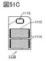
- 51A to 51E are schematic views of a storage device.
- 52A to 52H are diagrams showing electronic devices.
- the size, layer thickness, or area may be exaggerated for clarity. Therefore, it is not necessarily limited to that scale.
- the drawings schematically show ideal examples, and are not limited to the shapes or values shown in the drawings. For example, in an actual manufacturing process, layers, resist masks, etc. may be unintentionally reduced due to processing such as etching, but they may not be reflected in the figure for the sake of easy understanding. Further, in the drawings, the same reference numerals may be used in common between different drawings for the same parts or parts having similar functions, and the repeated description thereof may be omitted. Further, when referring to the same function, the hatch pattern may be the same and no particular sign may be added.
- a top view also referred to as a "plan view”
- a perspective view the description of some components may be omitted.
- some hidden lines may be omitted.
- the ordinal numbers attached as the first, second, etc. are used for convenience, and do not indicate the process order or the stacking order. Therefore, for example, the "first” can be appropriately replaced with the “second” or “third” for explanation.
- the ordinal numbers described in the present specification and the like may not match the ordinal numbers used to specify one aspect of the present invention.
- X and Y are connected, the case where X and Y are electrically connected and the case where X and Y function. It is assumed that the case where X and Y are directly connected and the case where X and Y are directly connected are disclosed in the present specification and the like. Therefore, it is not limited to the predetermined connection relationship, for example, the connection relationship shown in the figure or text, and other than the connection relationship shown in the figure or text, it is assumed that the connection relationship is disclosed in the figure or text.
- X and Y are assumed to be objects (for example, devices, elements, circuits, wirings, electrodes, terminals, conductive films, layers, etc.).
- a transistor is an element having at least three terminals including a gate, a drain, and a source. It also has a region (hereinafter, also referred to as a channel forming region) in which a channel is formed between the drain (drain terminal, drain region or drain electrode) and the source (source terminal, source region or source electrode). A current can flow between the source and the drain through the channel formation region.
- the channel formation region means a region in which a current mainly flows.
- source and drain functions may be interchanged when transistors with different polarities are used or when the direction of current changes during circuit operation. Therefore, in the present specification and the like, the terms source and drain may be used interchangeably.
- the channel length is, for example, the source in the top view of the transistor, the region where the semiconductor (or the portion where the current flows in the semiconductor when the transistor is on) and the gate electrode overlap each other, or the channel formation region.
- the channel length does not always take the same value in all regions. That is, the channel length of one transistor may not be fixed to one value. Therefore, in the present specification, the channel length is set to any one value, the maximum value, the minimum value, or the average value in the channel formation region.
- the channel width is, for example, the channel length direction in the region where the semiconductor (or the portion where the current flows in the semiconductor when the transistor is on) and the gate electrode overlap each other in the top view of the transistor, or the channel formation region. Refers to the length of the channel formation region in the vertical direction with reference to. In one transistor, the channel width does not always take the same value in all regions. That is, the channel width of one transistor may not be fixed to one value. Therefore, in the present specification, the channel width is set to any one value, the maximum value, the minimum value, or the average value in the channel formation region.
- the channel width in the region where the channel is actually formed (hereinafter, also referred to as “effective channel width”) and the channel width shown in the top view of the transistor. (Hereinafter, also referred to as “apparent channel width”) and may be different.
- the effective channel width may be larger than the apparent channel width, and the influence thereof may not be negligible.
- the proportion of the channel forming region formed on the side surface of the semiconductor may be large. In that case, the effective channel width is larger than the apparent channel width.
- channel width may refer to the apparent channel width.
- channel width may refer to an effective channel width.
- the channel length, channel width, effective channel width, apparent channel width, and the like can be determined by analyzing a cross-sectional TEM image or the like.
- the semiconductor impurities are, for example, other than the main components constituting the semiconductor.
- an element having a concentration of less than 0.1 atomic% can be said to be an impurity. Due to the inclusion of impurities, for example, the defect level density of the semiconductor may increase or the crystallinity may decrease.
- the impurities that change the characteristics of the semiconductor include, for example, Group 1 elements, Group 2 elements, Group 13 elements, Group 14 elements, Group 15 elements, and oxide semiconductors.
- transition metals other than the main component such as hydrogen, lithium, sodium, silicon, boron, phosphorus, carbon, and nitrogen. Water may also function as an impurity. Further, for example, by mixing of impurities, it may (may be referred to as V O.) Oxygen vacancies in the oxide semiconductor is formed.
- silicon oxide is composed of silicon oxide having a higher oxygen content than nitrogen.
- silicon nitride has a higher nitrogen content than oxygen in its composition.
- the term “insulator” can be paraphrased as an insulating film or an insulating layer.
- the term “conductor” can be rephrased as a conductive film or a conductive layer.
- semiconductor can be paraphrased as a semiconductor film or a semiconductor layer.
- parallel means a state in which two straight lines are arranged at an angle of -10 degrees or more and 10 degrees or less. Therefore, the case of -5 degrees or more and 5 degrees or less is also included.
- approximately parallel means a state in which two straight lines are arranged at an angle of -30 degrees or more and 30 degrees or less.
- vertical means a state in which two straight lines are arranged at an angle of 80 degrees or more and 100 degrees or less. Therefore, the case of 85 degrees or more and 95 degrees or less is also included.
- approximately vertical means a state in which two straight lines are arranged at an angle of 60 degrees or more and 120 degrees or less.
- a metal oxide is a metal oxide in a broad sense. Metal oxides are classified into oxide insulators, oxide conductors (including transparent oxide conductors), oxide semiconductors (also referred to as Oxide Semiconductor or simply OS) and the like. For example, when a metal oxide is used in the semiconductor layer of a transistor, the metal oxide may be referred to as an oxide semiconductor. That is, when it is described as an OS transistor, it can be rephrased as a transistor having a metal oxide or an oxide semiconductor.
- a metal oxide having nitrogen may also be collectively referred to as a metal oxide. Further, a metal oxide having nitrogen may be referred to as a metal oxynitride.
- normally off means that when a potential is not applied to the gate or a ground potential is applied to the gate, the drain current per 1 ⁇ m of the channel width flowing through the transistor is 1 ⁇ 10 ⁇ at room temperature. It means that it is 20 A or less, 1 ⁇ 10 -18 A or less at 85 ° C, or 1 ⁇ 10 -16 A or less at 125 ° C.
- FIG. 1 is a cross-sectional view of a transistor 10 having a metal oxide, which is one aspect of the present invention, in the channel length direction.
- the transistor 10 is arranged on an oxide 230 arranged on a substrate (not shown), an insulator 250 arranged on the oxide 230, and an insulator 250. It has a conductor 260 and the like. Further, the oxide 230 has a region 234 that functions as a region (hereinafter, also referred to as a channel formation region) in which a channel of the transistor 10 is formed, and a region 231a and a region 231b that function as a source region or a drain region. Have.
- the insulator 250 functions as a gate insulator. Further, the conductor 260 functions as a gate electrode.
- a conductor that functions as a source electrode or a drain electrode may be provided so as to be in contact with the oxide 230.
- a partially low resistance region is formed between the oxide 230 and the conductor or near the surface of the oxide 230. May be formed.
- oxygen deficiency, impurities (hydrogen, nitrogen, metal elements, etc.) that have entered the oxygen deficiency may function as donors, and the carrier concentration may increase.
- at least a part of the low resistance region is included in the region 231a or the region 231b that functions as a source region or a drain region.
- the transistor can control the resistance of the channel portion by the potential applied to the gate. That is, the continuity (transistor is on) and non-conductivity (transistor is off) between the source and the drain can be controlled by the potential applied to the gate.
- a metal oxide hereinafter, also referred to as an oxide semiconductor that functions as a semiconductor in the semiconductor layer including the channel forming region.
- the metal oxide that functions as a semiconductor preferably has a band gap of 2 eV or more, and more preferably 2.5 eV or more. As described above, by using a metal oxide having a large bandgap, the off-current of the transistor can be reduced.
- a transistor using an oxide semiconductor in the channel formation region has an extremely small leakage current (off current) in a non-conducting state, so that a semiconductor device with low power consumption can be provided.
- Oxide semiconductors are divided into single crystal oxide semiconductors and other non-single crystal oxide semiconductors.
- Examples of the non-single crystal oxide semiconductor include CAAC-OS (c-axis aligned cristalline oxide semiconductor), polycrystal oxide semiconductor, nc-OS (nanocrystalline oxide semiconductor), and pseudoamorphous oxide semiconductor (a-lique).
- OS aminophous-like oxide semiconductor) and amorphous oxide semiconductors.
- a metal oxide that increases the on-current of the transistor in the channel formation region of the transistor.
- the carrier flows from the source to the drain via the channel forming region. Therefore, the on-current of the transistor can be increased by providing a channel forming region in which carriers can easily flow in the channel length direction.
- a metal oxide is composed of a plurality of metal elements
- one of the scattering factors contributing to carrier transmission is the randomness of the arrangement of metal atoms at the cation site (so-called cation disorder). Therefore, in order to increase the mobility of the metal oxide used in the transistor, it is preferable that the cation disorder of the metal oxide is reduced.
- the crystal preferably has a crystal structure in which a first layer, a second layer, and a third layer are laminated. That is, the crystal has a layered crystal structure (also referred to as a layered crystal or a layered structure). At this time, the direction of the c-axis of the crystal is the direction in which the first layer, the second layer, and the third layer are laminated.
- the metal oxide having the crystal includes, for example, a single crystal oxide semiconductor, CAAC-OS described later, and the like.
- the c-axis of the crystal is oriented in the normal direction with respect to the surface to be formed or the surface of the film of the metal oxide.
- the first layer to the third layer are arranged substantially parallel to the surface to be formed or the surface of the film of the metal oxide. That is, the first layer to the third layer spread in the channel length direction.
- the first layer has an octahedral structure in which the metal atom of the first layer is present at the center and the oxygen atom is present at the apex.
- the second layer has a trigonal bipyramidal or tetrahedral structure in which the metal atom of the second layer is present at the center and the oxygen atom is present at the apex.
- the third layer has a trigonal bipyramidal or tetrahedral structure in which the metal atom of the third layer is present at the center and the oxygen atom is present at the apex.
- Examples of the crystal structure of the crystal include a YbFe 2 O 4 type structure, a Yb 2 Fe 3 O 7 type structure, and a modified structure thereof.
- each of the first layer to the third layer is preferably composed of one metal element or a plurality of metal elements having the same valence and oxygen. It is preferable that the valences of one or more metal elements constituting the first layer and the valences of one or more metal elements constituting the second layer are the same. Further, the first layer and the second layer may have the same metal element. Further, it is preferable that the valences of one or more metal elements constituting the first layer and the valences of one or more metal elements constituting the third layer are different.
- the cation disorder of the metal oxide can be reduced and the mobility of the metal oxide can be increased. Therefore, by using the metal oxide in the channel forming region of the transistor, the on-current of the transistor is increased, and the electrical characteristics of the transistor can be improved.
- the cation disorder of the metal oxide having crystals will be described later.
- the metal oxide preferably contains at least indium or zinc. In particular, it preferably contains indium and zinc. In addition to them, it is preferable that a metal element having the same valence as indium or zinc is contained. Examples of the metal element include aluminum, gallium, and yttrium. Further, one or more kinds selected from iron, cobalt, nickel, lanthanum, cerium, neodymium, magnesium, calcium and the like may be contained.
- the metal oxide is an In-M-Zn oxide having indium (In), element M, and zinc (Zn).
- the element M is aluminum, gallium, yttrium, or the like.
- Other elements applicable to element M include iron, cobalt, nickel, lanthanum, cerium, neodymium, magnesium, calcium and the like.
- the element M a plurality of the above-mentioned elements may be combined in some cases.
- the metal oxide is an In-M-Zn oxide
- the atomic arrangement in the crystal of the metal oxide will be described.
- FIGS. 2A to 2C are diagrams showing the atomic arrangement in the crystal of the oxide 230. 2A to 2C are also enlarged views of the region 51 of the oxide 230 shown in FIG.
- the element M is a + trivalent metal element.
- the element M is described as M 3+ for convenience.
- the atom is represented by a sphere (circle), and the bond between the metal atom (In, M 3+ , or Zn) and the oxygen atom (O) is represented by a line.
- the c-axis (c-axis) direction in the crystal structure of In—M—Zn oxide is indicated by an arrow. Further, the ab plane direction in the crystal structure of the In—M—Zn oxide is a direction perpendicular to the c-axis direction indicated by the arrow in FIGS. 2A to 2C.
- the crystals of the oxide 230 consist of a layer 21 having indium (In) and oxygen, a layer 31 having element M and oxygen, and a layer 41 having zinc (Zn) and oxygen, in that order. , Repeatedly laminated.
- the layer 21 corresponds to the first layer
- the layer 31 corresponds to the second layer
- the layer 41 corresponds to the third layer.
- each of the layer 21, layer 31, and layer 41 of the crystal is composed of one metal element and oxygen to reduce the cation disorder and reduce the metal oxide. Mobility can be increased.
- the stacking order of the layers 21, the layers 31, and the layers 41 is not limited to the stacking order shown in FIG. 2A, and the stacking order of the layers 31 and the layers 41 located between the two layers 21 does not matter.
- layer 21, layer 41, and layer 31 may be repeatedly laminated in this order, or as shown in FIG. 2B, layer 21, layer 41, layer 31, layer 21, layer 31, and layer 41 are repeated in this order. It may be laminated.
- the crystal of the oxide 230 includes a layer 22 having indium, an element M and oxygen, a layer 32 having indium, an element M and oxygen, and a layer 41 having zinc and oxygen. They are repeatedly laminated in order.
- the layer 22 corresponds to the first layer
- the layer 32 corresponds to the second layer.
- the stacking order of the layers 22, the layers 32, and the layers 41 is the same as the stacking order of the layers 21, the layers 31, and the layers 41, and the stacking order of the layers 32 and the layers 41 located between the two layers 22 is not limited. Absent.
- the atomic number ratio of indium to the element M in the layer 22 is preferably larger than the atomic number ratio of indium to the element M in the layer 32. This facilitates the formation of crystals in the In-M-Zn oxide.
- FIGS. 2A to 2C the atomic arrangement in the crystal is represented by a sphere (circle) and a line.
- the atomic arrangement in the crystal is displayed as a polyhedron.
- FIG. 3A is a view showing the atomic arrangement in the crystal shown in FIG. 2A as a polyhedron.
- the polyhedron of the layer 21 is shown in FIG. 3B
- the polyhedron that the layer 31 can have is shown in FIG. 3C
- the polyhedron that the layer 41 can have is shown in FIG. 3D.
- the polyhedron shown in FIG. 3B has an octahedral structure.
- the octahedral structure has an indium atom at the center and an oxygen atom at the apex.
- the octahedral structure shares a ridge.
- an atom of the element M may be present at the center of the octahedral structure.
- the polyhedron shown in FIG. 3C has a trigonal bipyramidal structure.
- the trigonal bipyramidal structure has an atom of element M or an atom of zinc in the center and an atom of oxygen at the apex.
- the polyhedron shown in FIG. 3D has a tetrahedral structure.
- the tetrahedral structure has a zinc atom at the center and an oxygen atom at the apex.
- the trigonal bipyramidal structure shares a ridge.
- the trigonal bipyramidal structure shares vertices.
- the tetrahedral structure shares vertices. Indium atoms may be present at the center of the trigonal bipyramidal structure.
- Layer 21 and layer 31 or layer 41 share vertices. Further, the layer 31 and the layer 41 share vertices or ridges.
- the composition of oxide 230 is not limited to this.
- Oxide 230 is crystalline, for example, having a composition formula of In (1 + ⁇ ) M (1- ⁇ ) O 3 (ZnO) m ( ⁇ is a real number greater than 0 and less than 1 and m is a positive number).
- In—M—Zn oxide may be used.
- m is a real number larger than 0 and smaller than 1
- a part of the layers located between the two existing layers 21 may be composed of only the layer 31.
- m is a real number larger than 1
- a part of the layers located between the two existing layers 21 may be composed of the layer 31 and two or more layers 41. is there.
- the In-M-Zn oxide containing a + trivalent metal element (element Ma) and a + divalent metal element (element Mb) as the element M is oxygen with either one or both of indium and element Ma.
- the path through which carriers that is, the wave function of the conduction band
- carriers also called conduction electrons
- the wave function of the conduction band is important.
- the wave function of the conduction band is localized, carrier transmission is suppressed and mobility is reduced. Therefore, the first-principles calculation in this section is performed focusing on the distribution of the valence of the cation and the localization of the wave function of the conduction band in the crystal structure of the In-Ga-Zn oxide.
- the crystal structure has a layered structure shown in FIG. 2A, and the cation site of the layer located between the layers having In and O has a Ga valence of +3 or a valence of +2.
- Zn is arranged.
- Figure 4A shows the calculation model.
- the c-axis direction of the calculation model is represented by a solid arrow.
- the b-axis direction of the calculation model is indicated by a broken line arrow.
- the a-axis direction of the calculation model is the c-axis direction represented by the solid arrow and the direction perpendicular to the b-axis direction represented by the broken arrow.
- the a-c plane is in the direction perpendicular to the b-axis direction indicated by the broken line arrow.
- the number of atoms arranged in the calculation model is 288.
- FIG. 4B shows the number of Ga atoms in the ac plane.
- the horizontal axis is the coordinates along the b-axis
- the vertical axis is the number of Ga atoms in the ac plane.
- the calculation model shows a region in which Ga atoms are aggregated in the ac plane (a region in which the number of Ga atoms is 2 in FIG. 4B) and a Zn in the ac plane.
- a region where atoms are aggregated (a region in which the number of Ga atoms is 0 in FIG. 4B) is provided.
- the first-principles calculation software VASP Vienna Ab initio simulation Package
- the calculation conditions are shown in Table 1.
- the potential generated by the Projector Augmented Wave (PAW) method was used for the electronic state pseudopotential, and GGA-PBE (Generialized-Gradient-Approximation-Perdew-Burke-Ernzerhof) was used for the functional.
- PAW Projector Augmented Wave
- GGA-PBE Generialized-Gradient-Approximation-Perdew-Burke-Ernzerhof
- the wave function at the lower end of the conduction band obtained by the above calculation is projected along the b-axis.
- the square of the absolute value of the wave function at the lower end of the conduction band projected along the b-axis is calculated.
- the square of the absolute value of the wave function is sometimes called the electron density.
- FIG. 4C shows the electron density at the lower end of the conduction band projected along the b-axis direction.
- the horizontal axis is the coordinates [nm] along the b-axis
- the vertical axis is the electron density (Electron Density) [a.]
- the electron density at the lower end of the conduction band is localized around the region where Ga atoms are aggregated. That is, the wave function at the lower end of the conduction band is localized in the region where Ga atoms are aggregated. In other words, it is suggested that conduction electrons are localized in the region where Ga atoms are aggregated.
- LDOS local density of states
- E energy
- x, y, and z are coordinates
- ⁇ is the blur width
- ⁇ is the wave function
- ⁇ is the eigenvalue
- Figure 4D shows the calculated LDOS map.
- the horizontal axis is the coordinates [nm] along the b-axis
- the vertical axis is the energy [eV]. Specifically, the darker the color (black), the larger the LDOS value, and the lighter the color (white), the smaller the LDOS value.
- the upper end of the valence band is located on the low energy side among the energy values at which the LDOS value changes significantly.
- the energy value at the upper end of the valence band is located near 0 eV.
- the lower end of the conduction band is located on the high energy side among the energy values at which the LDOS value changes significantly.
- the energy value at the lower end of the conduction band is located near 1.5 eV.
- the lower end of the conduction band is recessed toward the low energy side in the region where Ga atoms are aggregated.
- the conduction band also called a band
- the bending of the band is saturated from the agglutination region of Ga to the region with less Ga (more Zn), and after that (the value on the horizontal axis is near 0 nm or around 5 nm), a flat band is formed. It can be seen that it is forming.
- Ga having a large valence is localized (the valence is biased), so that the electrostatic potential is inclined. Then, it is presumed that the localization of the wave function at the lower end of the conduction band (localization of conduction electrons) occurs when an electric field is applied and the band bends.
- Ga atoms agglutinate (the valences are biased), causing band bending (localization of conduction electrons), which is a scattering source of electrical conduction. It occurs and is suggested to cause a decrease in mobility. Therefore, by suppressing the aggregation of Ga atoms, it is possible to suppress the decrease in mobility.
- FIG. 5A shows a calculation model different from the calculation model used for the above calculation.
- the calculation model shown in FIG. 5A is a crystal model of IGZO composed of In, Ga, Zn, and O.
- Region 901 corresponds to the channel formation region
- region 902 corresponds to one of the source and drain regions
- region 903 corresponds to the other of the source and drain regions.
- the a-axis direction is the direction from the region 902 to the region 903, and the c-axis direction is a layer composed of In and O (sometimes referred to as an InO layer). ), And the b-axis direction is the direction perpendicular to the a-axis direction and the c-axis direction.
- model 1A to model 1E a calculation model in which the region 902 and the region 903 are common and the arrangement of the cations in the region 901 is different is prepared.
- the area 901 of model 1A is shown in FIG. 5B
- the area 901 of model 1B is shown in FIG. 6A
- the area 901 of model 1C is shown in FIG. 6B
- the area 901 of model 1D is shown in FIG. 6C
- model 1E Region 901 is illustrated in FIG. 6D.
- the region 911a shown in FIG. 5B is a region in the model 1A where the cation arrangement is exchanged.
- Regions 912a and 913a are fixed layers in model 1A.
- the fixed layer corresponds to the electrode region (region 902 or region 903) in the conduction calculation.
- the model 1A has an arrangement in which the Ga atoms are not biased with respect to the a-axis and the c-axis.
- the region 911b shown in FIG. 6A is a region in the model 1B where the cation arrangement is exchanged. Regions 912b and 913b are fixed layers in model 1B. In the region 911b, the cation arrangement of the region surrounded by the dotted line in FIG. 6A is different from that of the region 911a. Specifically, the region 911b has an arrangement in which Ga and Zn at the same location in the region 911a are interchanged in the region surrounded by the dotted line in FIG. 6A. That is, model 1B has an arrangement in which Ga atoms are biased with respect to the a-axis.
- the region 911c shown in FIG. 6B is a region in the model 1C where the cation arrangement is exchanged. Regions 912c and 913c are fixed layers in model 1C. In the region 911c, the cation arrangement of the two regions surrounded by the dotted line in FIG. 6B is different from that of the region 911a. Specifically, the region 911c has an arrangement in which Ga and Zn at the same location in the region 911a are interchanged in each of the two regions surrounded by the dotted line in FIG. 6A. That is, the model 1C has an arrangement in which the Ga atoms are not biased with respect to the a-axis and the c-axis.
- the region 911d shown in FIG. 6C is a region in the model 1D where the cation arrangement is exchanged. Regions 912d and 913d are fixed layers in model 1D.
- the region 911d differs from the region 911a in the cation arrangement of the region surrounded by the dotted line and the region surrounded by the broken line in FIG. 6C. Specifically, the region 911d has an arrangement in which the cation of the region 911a corresponding to the region surrounded by the dotted line in FIG. 6C and the cation of the region 911a corresponding to the region surrounded by the broken line in FIG. 6C are interchanged. That is, the model 1D has a biased arrangement of Ga atoms with respect to the c-axis.
- the region 911e shown in FIG. 6D is a region in the model 1E where the cation arrangement is exchanged. Regions 912e and 913e are fixed layers in model 1E.
- the region 911e differs from the region 911a in the cation arrangement of the region surrounded by the dotted line and the region surrounded by the broken line in FIG. 6D.
- the region 911e has an arrangement in which the cation of the region 911a corresponding to the region surrounded by the dotted line in FIG. 6D and the cation of the region 911a corresponding to the region surrounded by the broken line in FIG. 6D are interchanged. That is, the model 1E has an arrangement in which the Ga atom is biased with respect to the a axis.
- the DFT + U method is applied in the first-principles calculation.
- on-site Coulomb U parameters (U-parameters) are set for each of the atoms (In, Ga, Zn, O in the case of IGZO) constituting the calculation model.
- the U parameter of the metal atom (In, Ga, Zn) is set to 10 eV
- the U parameter of the oxygen atom is set to 20 eV.
- the value of the band gap obtained by calculation can be set to a value close to the actually measured band gap.
- FIG. 7A shows a map of LDOS calculated for model 1A.
- the horizontal axis is the coordinates [nm] in the a-axis direction
- the vertical axis is the energy [eV].
- E F shown in FIG. 7A is a Fermi energy.
- FIG. 7B shows the density of states calculated for model 1A.
- the horizontal axis is the density of states [states / eV] and the vertical axis is the energy [eV].
- E F shown in FIG. 7B is a Fermi energy
- E VBM is the energy of a valence band upper end
- E CBM is the energy of the conduction band minimum.
- FIG. 8A shows the number of Ga atoms in the bc plane in model 1B. Further, FIG. 8B shows the number of Ga atoms in the bc plane in the model 1C. Further, FIG. 9A shows the number of Ga atoms in the bc plane in the model 1D. Further, FIG. 9B shows the number of Ga atoms in the bc plane in the model 1E.
- the horizontal axis corresponds to the coordinates in the a-axis direction, and the vertical axis represents the number of Ga atoms in the bc plane.
- the model 1B and the model 1E have an arrangement in which the Ga atom is biased with respect to the a axis. Further, as shown in FIGS. 8B and 9A, the models 1C and 1D have an arrangement in which the Ga atoms are not biased with respect to the a-axis.
- FIG. 8C shows a map of LDOS calculated for model 1B. Further, FIG. 8D shows a map of LDOS calculated for model 1C. Further, FIG. 9C shows a map of LDOS calculated for model 1D. Further, FIG. 9D shows a map of LDOS calculated for model 1E.
- the horizontal axis is the coordinates [nm] in the a-axis direction, and the vertical axis is the energy [eV]. Specifically, the darker the color (black), the larger the LDOS value, and the lighter the color (white), the smaller the LDOS value.
- the arrangement of Ga atoms biased with respect to the a-axis forms an electric dipole due to the difference between the valence of Ga (+3 valence) and the valence of Zn (+2 valence), and the electrostatic potential. Is presumed to tilt. At this time, the lower end of the conduction band moves up and down, and the conduction of carriers (mainly electrons in the case of IGZO) is hindered. Therefore, it is presumed that carrier scattering occurs in the real space. On the other hand, the arrangement of Ga atoms without bias with respect to the a-axis suggests that carrier scattering does not occur.
- the conductance and transmittance are calculated by performing the conduction calculation based on the first principle using the non-equilibrium Green's function (NEGF) method.
- NEGF non-equilibrium Green's function
- Conductance is the reciprocal of electrical resistance and is an index that indicates the ease with which electricity can flow.
- the conductance G is calculated by the following formula.
- the conductance G can be calculated by calculating the transmittance T (E) in the energy E.
- the transmittance T (E) in the energy E may be simply referred to as the transmittance T.
- the transmittance T (E) in the energy E is calculated by the following formula.
- ⁇ L (E) and ⁇ R (E) are self-energy in energy E
- G (E) is Green's function in energy E.
- the DFT + U method is applied in the first-principles calculation.
- the U parameter of the metal atom In, Ga, Zn
- the U parameter of the oxygen atom is set to 3.7 eV.
- the value of the band gap obtained by calculation can be set to a value close to the actually measured band gap.
- FIGS. 10A and 10B The spectra of the transmittances of models 1A to 1E obtained by calculation using the NEGF method are shown in FIGS. 10A and 10B.
- FIG. 10A is a spectrum of the transmittance of each model near the band gap
- FIG. 10B is a spectrum of the transmittance of each model at the lower end of the conduction band and its vicinity.
- the horizontal axis is energy [eV]
- the vertical axis is transmittance T.
- the transmittance of model 1A is the highest among models 1A to 1E. It can also be seen that the transmittance of model 1E is the lowest. It can be seen that the transmittances of the model 1C and the model 1D at the lower end of the conduction band and its vicinity are almost the same as the transmittance of the model 1A.
- FIG. 11 shows the transmittance spectrum of model 1A and the shape obtained by differentiating the Fermi distribution function.
- the horizontal axis is energy [eV]
- the first vertical axis (vertical axis on the left side) is the transmittance T
- the second vertical axis (vertical axis on the right side) is the differentiation of the Fermi distribution function [/ eV]. ].
- the solid line shown in FIG. 11 is the spectrum of the transmittance of the model 1A
- the dotted line shown in FIG. 11 is a shape obtained by differentiating the Fermi distribution function.
- the Fermi distribution function is calculated assuming that the carrier concentration is 6 ⁇ 10 20 cm -3 and the electron temperature is 300 K.
- Table 4 shows the conducted conductance calculated for each of the models 1A to 1E.
- model 1A is the largest and the conductance of model 1E is the smallest.
- the conductance of the model 1C and the model 1D is almost the same as the conductance of the model 1A.
- FIGS. 12 and 13A to 13D show the transmitted electron densities in models 1A to 1E.
- the surfaces shown in mesh in FIGS. 12 and 13A to 13D are equal surface surfaces of electron density, having a carrier concentration of 6 ⁇ 10 20 cm -3 and an isosurface level of 22 nm -3. Is.
- the InO layer has a continuous transmitted electron density. Further, it is confirmed that the transmitted electron density exists around the Ga atom as compared with the Zn atom. Therefore, it is presumed that the Ga atom contributes more to carrier transport than the Zn atom. It is also confirmed that the transmitted electron density derived from the s orbital of the O atom exists. Therefore, it is presumed that the conduction of the s orbital of the O atom cannot be ignored.
- model 1B although carriers are scattered in and near the region where the band is curved, some carriers are transmitted. From FIG. 13B, carrier scattering is not clearly observed in model 1C. From FIG. 13C, it is suggested that in model 1D, the carrier selectively conducts the position of the Ga atom. From FIGS. 9D and 13D, it can be seen that in model 1E, carrier scattering occurs in and near the region where the band is curved, and the carriers are hardly transmitted.
- the transmittance decreases due to the irregular arrangement of cations (Ga, Zn). It can be seen that this tendency is particularly remarkable in a structure in which the number of Ga atoms is biased with respect to the conduction direction. In addition, it can be seen that the band is greatly bent in the structure in which the transmittance is significantly reduced. Moreover, it can be seen that the main conduction paths exist in In and Ga, which have high valences. In addition, it can be seen that the transmittance is greatly reduced in the region where the band is curved and in the vicinity thereof.
- a method for forming a metal oxide As a method for forming a metal oxide, a sputtering method, a chemical vapor deposition (CVD) method, a molecular beam epitaxy (MBE) method, a pulsed laser deposition (PLD) method, and a pulse laser deposition (PLD) method are used. There is an atomic layer deposition (ALD: Atomic Layer Deposition) method and the like.
- the ALD method can be used as a method for forming a metal oxide.
- the ALD method utilizes the characteristics of the precursor molecules or the atoms contained in the precursor to deposit atoms layer by layer, enabling ultra-thin film formation and formation into a structure with a high aspect ratio. It has the effects of being possible, being able to form a film with few defects such as pinholes, being able to form a film with excellent coverage, and being able to form a film at a low temperature.
- the ALD method also includes a plasma ALD (PEALD: Plasma Enhanced ALD) method, which is a film formation method using plasma. By using plasma, it is possible to form a film at a lower temperature, which may be preferable.
- Some precursors used in the ALD method contain elements such as carbon and chlorine.
- the film provided by the ALD method may contain a large amount of elements such as carbon and chlorine as compared with the film provided by other film forming methods.
- the quantification of these elements can be performed using X-ray photoelectron spectroscopy (XPS: X-ray Photoelectron Spectroscopy).
- the ALD method is a film forming method in which a film is formed by a reaction on the surface of an object to be treated, unlike a film forming method in which particles emitted from a target or the like are deposited. Therefore, it is a film forming method that is not easily affected by the shape of the object to be treated and has good step coverage.
- the ALD method has excellent step covering property and excellent thickness uniformity, and is therefore suitable for covering the surface of an opening having a high aspect ratio.
- the ALD method since the ALD method has a relatively slow film formation rate, it may be preferable to use it in combination with another film formation method such as a CVD method having a high film formation rate.
- the composition of the obtained film can be controlled by the amount of the raw material gas introduced.
- a film having an arbitrary composition can be formed depending on the amount of the raw material gas introduced and the number of times of introduction (also referred to as the number of pulses).
- a film having a continuously changed composition can be formed by changing the raw material gas while forming the film.
- ALD apparatus a film forming apparatus using the ALD method (hereinafter, also referred to as an ALD apparatus) that can be used for forming the metal oxide of one aspect of the present invention, and a film forming method using the ALD method will be described.
- the deposition apparatus using the ALD method alternately introduces the first raw material gas (also called precursor, precursor, metal precursor) and the second raw material gas (also called reactant, reactor, non-metal precursor) into the chamber. Then, the film is formed by repeating the introduction of these raw material gases.
- the introduction of the raw material gas can be switched, for example, by switching each switching valve (also referred to as a high-speed valve).
- an inert gas such as nitrogen (N 2 ) or argon (Ar) may be introduced into the chamber together with the raw material gas as a carrier gas.
- the first raw material gas is introduced into the chamber (see FIG. 14A), and the precursor 601 is adsorbed on the substrate surface (first step).
- the precursor 601 is adsorbed on the surface of the substrate, the self-stop mechanism of the surface chemical reaction acts, and the precursor is not further adsorbed on the layer of the precursor on the substrate (see FIG. 14B).
- the appropriate range of the substrate temperature on which the self-stop mechanism of the surface chemical reaction acts is also called ALD Window.
- the ALD window is determined by the temperature characteristics, vapor pressure, decomposition temperature, etc. of the precursor, but is 100 ° C. or higher and 500 ° C.
- a Reactant 602 for example, an oxidizing agent (ozone (O 3 ), oxygen (O 2 ), water (H 2 O), and their plasma, radicals, ions, etc.) is chambered. (See FIG.
- ozone, oxygen, or water when used as a reactor or an oxidizing agent, these are not limited to gas and molecular states, but are plasma states and radical states. , And those in the ionic state are also included.
- a radical ALD device or a plasma ALD device described later When forming a film using an oxidizing agent in a plasma state, a radical state, or an ionic state, a radical ALD device or a plasma ALD device described later may be used.
- water as an oxidizing agent to remove carbon contained in the precursor. Hydrogen contained in water reacts with carbon contained in the precursor, and carbon can be efficiently released from the precursor. On the other hand, when it is desired to reduce hydrogen contained in the formed film as much as possible, it is preferable to use ozone or oxygen containing no hydrogen as an oxidizing agent.
- ozone or oxygen containing no hydrogen as an oxidizing agent.
- water by introducing water into the chamber as the first oxidant, carbon contained in the precursor is removed, and then vacuum exhaust is performed, and ozone and oxygen containing no hydrogen are introduced into the chamber as the second oxidant. The hydrogen may be removed and vacuum exhaust may be performed. Then, the first step to the fourth step are repeated until a desired film thickness is obtained.
- the second source gas may be introduced into the chamber and then the first source gas may be introduced into the chamber. That is, the third step is performed first, then the fourth step is performed, then the first step, the second step, the third step, and the fourth step are performed, and then the first step to the fourth step are repeated.
- the film may be formed with. Further, the film may be formed by repeating the third step and the fourth step a plurality of times and then repeating the first step to the fourth step.
- the film formation atmosphere in the chamber can be controlled.
- an oxygen atmosphere can be created in the chamber by introducing an oxidizing agent.
- the oxygen concentration in the formed film can be increased, which is preferable.
- oxygen can be supplied to the insulator and oxide that are the base of the film.
- the semiconductor device formed by using such a method has good characteristics and can obtain high reliability.
- the introduction of the second raw material gas in the third step and the introduction of the vacuum exhaust or the inert gas in the fourth step may be repeated a plurality of times. That is, after repeating the first step, the second step, the third step, the fourth step, the third step, the fourth step, and the third step and the fourth step, the first step and the second step are performed. You may.
- O 3 and O 2 may be introduced as oxidizing agents in the third step, vacuum exhaust may be performed in the fourth step, and this step may be repeated a plurality of times.
- H 2 O may be used as the oxidizing agent in the first third step
- O 3 may be used as the oxidizing agent in the second and subsequent third steps.
- the amount of water molecules desorbed is 1.0 ⁇ 10 13 membrane / cm 2 in the range of surface temperature of 100 ° C. or higher and 700 ° C. or lower or 100 ° C. or higher and 500 ° C. or lower in TDS analysis.
- a film having a size of 1.0 ⁇ 10 16 molecule / cm 2 or less, preferably 1.0 ⁇ 10 13 molecule / cm 2 or more and 3.0 ⁇ 10 15 molecule / cm 2 or less can be formed.
- the first layer can be formed on the surface of the substrate, and by performing the first step to the fourth step again, the second layer can be laminated on the first layer. ..
- the first step to the fourth step a plurality of times until the film has a desired thickness while controlling the gas introduction, a thin film having excellent step covering property can be formed. Since the thickness of the thin film can be adjusted by the number of repetitions, the film thickness can be precisely adjusted, which is suitable for manufacturing a fine transistor.
- the film formed by the above method may have a layered structure. Further, when the film formed by the above method has a crystal structure, the c-axis of the film is oriented in a direction substantially parallel to the normal direction of the surface to be formed. That is, the c-axis of the film is oriented perpendicular to the surface to be filmed.
- a crystal structure may be referred to as a CAAC structure
- an oxide semiconductor (metal oxide) having a CAAC structure may be referred to as CAAC-OS.
- ALD method it is possible to form a metal oxide having a CAAC structure.
- the ALD method is a film formation method performed by reacting a precursor and a reactor using thermal energy.
- the temperature required for the reaction of the precursor and the reactor is determined by their temperature characteristics, vapor pressure, decomposition temperature and the like, but is 100 ° C. or higher and 500 ° C. or lower, preferably 200 ° C. or higher and 400 ° C. or lower.
- the ALD method in which the plasma-excited reactor is also introduced into the chamber as the third raw material gas to perform the treatment may be called the plasma ALD method.
- a plasma generator is provided at the introduction portion of the third raw material gas.
- ICP Inductively coupled plasma
- the ALD method in which the reaction of the precursor and the reactor is performed by thermal energy is sometimes called a thermal ALD method.
- a plasma-excited reactor is introduced in the third step to form a film.
- the film formation is performed by repeating the first step to the fourth step and at the same time introducing a plasma-excited reactor (second reactor).
- the reactor introduced in the third step is called the first reactor.
- the same material as the above-mentioned oxidizing agent can be used as the second reactorant used for the third raw material gas. That is, plasma-excited ozone, oxygen, and water can be used as the second reactor. Further, as the second reactor, a nitriding agent may be used in addition to the oxidizing agent.
- nitriding agent nitrogen (N 2 ) or ammonia (NH 3 ) can be used. Further, a mixed gas of nitrogen (N 2 ) and hydrogen (H 2 ) can be used as the nitriding agent. For example, a mixed gas of 5% nitrogen (N 2 ) and 95% hydrogen (H 2 ) can be used as the nitriding agent.
- a nitride film such as a metal nitride film can be formed by forming a film while introducing plasma-excited nitrogen or ammonia.
- argon (Ar) or nitrogen (N 2 ) may be used as the carrier gas of the second reactor. It is preferable to use a carrier gas such as argon or nitrogen because the plasma can be easily discharged and a second plasma-excited reactor can be easily generated.
- nitrogen is used as the carrier gas, nitrogen may be mixed in the film and the desired film quality may not be obtained. In this case, it is preferable to use argon as the carrier gas.
- the ALD method can form an extremely thin film with a uniform film thickness.
- the surface coverage is high even for surfaces with irregularities.
- the plasma ALD method it is possible to form a film at a lower temperature than the thermal ALD method.
- the plasma ALD method can form a film even at 100 ° C. or lower without lowering the film forming rate.
- not only an oxidizing agent but also many reactors such as a nitride can be used, so that not only oxides but also many kinds of films such as nitrides, fluorides and metals can be formed. Can be done.
- plasma can be generated in a state away from the substrate like ICP or the like. By generating plasma in this way, plasma damage can be suppressed.
- a film, an oxide film, or a nitride film containing an atom contained in the first raw material gas as one component can be formed.
- a plurality of precursors may be prepared for each metal and sequentially introduced into the chamber.
- In-M-Zn oxide When forming In-M-Zn oxide as a metal oxide, a raw material gas containing a first precursor containing indium is introduced into the chamber, and excess raw material gas is exhausted (purged). Next, as a reactor, an oxidant is introduced into the chamber and excess reactor is exhausted. Next, the raw material gas containing the second precursor containing the element M is introduced into the chamber, and the excess raw material gas is exhausted (purged). Next, as a reactor, an oxidant is introduced into the chamber and excess reactor is exhausted. Next, a raw material gas containing a third precursor containing zinc is introduced into the chamber, and excess raw material gas is exhausted (purged). Next, as a reactor, an oxidant is introduced into the chamber and excess reactor is exhausted. By repeating the above steps, a metal oxide containing a layer containing indium, a layer containing the element M, and a layer containing zinc can be formed.
- the order of introducing the raw material gas is not limited to the above. After the introduction of the raw material gas containing the first precursor, the raw material gas containing the third precursor may be introduced, and then the raw material gas containing the second precursor may be introduced, depending on the required properties of the membrane. Can be decided as appropriate. Further, after the introduction of each raw material gas, the excess raw material gas can be exhausted, the reactor can be introduced, and the exhaust can be appropriately performed.
- the metal oxide is not limited to In—M—Zn oxide. As described above, the metal oxide preferably contains at least indium or zinc, and particularly preferably contains indium and zinc. Further, the type of metal contained in the metal oxide may be two types or four or more types.
- introduction of a raw material gas The order is not limited to the above.
- m is a real number larger than 0 and less than 1
- the reactor After the introduction of each raw material gas, the excess raw material gas can be exhausted, the reactor can be introduced, and the exhaust can be appropriately performed.
- m is a real number larger than 1
- the raw material gas containing the second precursor is introduced after the introduction of the raw material gas containing the first precursor, and the raw material gas containing the third precursor is introduced a plurality of times.
- a step of introducing a raw material gas containing a first precursor may be performed.
- the order of introduction of the raw material gas containing the second precursor and the raw material gas containing the third precursor is not limited to the above. Further, after the introduction of each raw material gas, the excess raw material gas can be exhausted, the reactor can be introduced, and the exhaust can be appropriately performed.
- the atomic number ratio of the metal contained in the metal oxide can be controlled by adjusting the number of times the raw material gas containing the precursor containing the desired metal is introduced into the chamber and the film formation temperature. For example, when it is desired to increase the atomic number ratio of the element M to indium or zinc, a raw material gas containing a second precursor containing the element M is introduced into the chamber, the excess raw material gas is exhausted, and the reactor is used. After introducing the oxidant into the chamber and exhausting the excess reactorant, the raw material gas containing the second precursor containing the element M is introduced into the chamber again, the excess raw material gas is exhausted, and the oxidant is used as the reactor in the chamber. It can be introduced into the chamber and the excess reactor can be exhausted.
- a plurality of precursors may be introduced into the chamber.
- a raw material gas containing a first precursor and a second precursor is introduced into the chamber, excess raw material gas is exhausted, and a reactor is introduced into the chamber.
- Exhaust the excess Reactant introduce the raw material gas containing the first precursor and the second precursor into the chamber, exhaust the excess raw material gas, introduce the Reactant into the chamber, exhaust the excess Reactant,
- the metal oxide containing the In-M-Zn oxide is discharged. May be formed.
- the combination of precursors to be introduced into the above chamber assumes the case where the valence of the element M is +3 valence, but when the valence of the element M is +2 valence, the second precursor and the second precursor. It is advisable to introduce the raw material gas containing the precursor of No. 3 into the chamber.
- the raw material gas containing different precursors may be continuously introduced into the chamber.
- the reactor is not introduced into the chamber, and then the raw material gas containing the second precursor is introduced into the chamber.
- Exhaust the excess source gas introduce the reactor into the chamber, exhaust the excess reactor, introduce the source gas containing the first precursor into the chamber, exhaust the excess source gas, and then introduce the reactor into the chamber.
- the raw material gas containing the second precursor is introduced into the chamber, the excess raw material gas is exhausted, the reactor is introduced into the chamber, the excess reactor is exhausted, and the raw material gas containing the third precursor is exhausted.
- the order and combination of precursors continuously introduced into the chamber are not limited to the above. After introducing the raw material gas containing the second precursor into the chamber, the raw material gas containing the first precursor may be introduced into the chamber. Further, the order and combination of the precursors continuously introduced into the chamber described above assume that the valence of the element M is +3 valence, but when the valence of the element M is +2 valence, After introducing the raw material gas containing the second precursor into the chamber, it is preferable to introduce the raw material gas containing the third precursor into the chamber without introducing the reactor.
- a metal oxide may be formed by using a precursor containing a plurality of metals. For example, metal oxidation using a precursor containing indium and an element M having a valence of +3 in one molecule, a precursor containing an element M having a valence of +2 valence in one molecule, and zinc. You may form an object.
- CAAC-OS is an oxide semiconductor having a plurality of crystal regions, the plurality of crystal regions having the c-axis oriented in a specific direction.
- the specific direction is the thickness direction of the CAAC-OS film, the normal direction of the surface to be formed of the CAAC-OS film, or the normal direction of the surface of the CAAC-OS film.
- the crystal region is a region having periodicity in the atomic arrangement. When the atomic arrangement is regarded as a lattice arrangement, the crystal region is also a region in which the lattice arrangement is aligned. Further, the CAAC-OS has a region in which a plurality of crystal regions are connected in the ab plane direction, and the region may have distortion.
- the strain refers to a region in which a plurality of crystal regions are connected in which the orientation of the lattice arrangement changes between a region in which the lattice arrangement is aligned and a region in which another grid arrangement is aligned.
- CAAC-OS is an oxide semiconductor that is c-axis oriented and not clearly oriented in the ab plane direction.
- Each of the plurality of crystal regions is composed of one or a plurality of minute crystals (crystals having a maximum diameter of less than 10 nm).
- the maximum diameter of the crystal region is less than 10 nm.
- the size of the crystal region may be about several tens of nm.
- CAAC-OS has indium (In) and oxygen. It tends to have a layered crystal structure (also referred to as a layered structure) in which a layer (hereinafter, In layer) and a layer having elements M, zinc (Zn), and oxygen (hereinafter, (M, Zn) layer) are laminated. There is. Indium and element M can be replaced with each other. Therefore, the (M, Zn) layer may contain indium. In addition, the In layer may contain the element M. In addition, Zn may be contained in the In layer.
- the layered structure is observed as a lattice image in, for example, a high-resolution TEM image.
- the position of the peak indicating the c-axis orientation may vary depending on the type and composition of the metal elements constituting CAAC-OS.
- a plurality of bright spots are observed in the electron diffraction pattern of the CAAC-OS film. Note that a certain spot and another spot are observed at point-symmetrical positions with the spot of the incident electron beam passing through the sample (also referred to as a direct spot) as the center of symmetry.
- the lattice arrangement in the crystal region is based on a hexagonal lattice, but the unit lattice is not limited to a regular hexagon and may be a non-regular hexagon. Further, in the above strain, it may have a lattice arrangement such as a pentagon or a heptagon.
- a clear grain boundary cannot be confirmed even in the vicinity of strain. That is, it can be seen that the formation of grain boundaries is suppressed by the distortion of the lattice arrangement. This is because CAAC-OS can tolerate distortion because the arrangement of oxygen atoms is not dense in the ab plane direction and the bond distance between atoms changes due to substitution of metal atoms. It is thought that this is the reason.
- CAAC-OS for which no clear crystal grain boundary is confirmed, is one of the crystalline oxides having a crystal structure suitable for the semiconductor layer of the transistor.
- a configuration having Zn is preferable.
- In-Zn oxide and In-Ga-Zn oxide are more suitable than In oxide because they can suppress the generation of grain boundaries.
- CAAC-OS is an oxide semiconductor with high crystallinity and no clear grain boundaries can be confirmed. Therefore, it can be said that CAAC-OS is unlikely to cause a decrease in electron mobility due to grain boundaries. Further, since the crystallinity of the oxide semiconductor may be lowered due to the mixing of impurities or the generation of defects, CAAC-OS can be said to be an oxide semiconductor having few impurities and defects (oxygen deficiency, etc.). Therefore, the oxide semiconductor having CAAC-OS has stable physical properties. Therefore, the oxide semiconductor having CAAC-OS is resistant to heat and has high reliability. CAAC-OS is also stable against high temperatures in the manufacturing process (so-called thermal budget). Therefore, if CAAC-OS is used for the OS transistor, the degree of freedom in the manufacturing process can be expanded.
- the oxide semiconductor as a transistor, a transistor with high field effect mobility can be realized. Moreover, a highly reliable transistor can be realized.
- the carrier concentration of the oxide semiconductor is 1 ⁇ 10 17 cm -3 or less, preferably 1 ⁇ 10 15 cm -3 or less, more preferably 1 ⁇ 10 13 cm -3 or less, and more preferably 1 ⁇ 10 11 cm ⁇ . It is 3 or less, more preferably less than 1 ⁇ 10 10 cm -3 , and more than 1 ⁇ 10 -9 cm -3 .
- the impurity concentration in the oxide semiconductor film may be lowered to lower the defect level density.
- a low impurity concentration and a low defect level density is referred to as high-purity intrinsic or substantially high-purity intrinsic.
- An oxide semiconductor having a low carrier concentration may be referred to as a high-purity intrinsic or substantially high-purity intrinsic oxide semiconductor.
- the trap level density may also be low.
- the charge captured at the trap level of the oxide semiconductor takes a long time to disappear, and may behave as if it were a fixed charge. Therefore, a transistor in which a channel forming region is formed in an oxide semiconductor having a high trap level density may have unstable electrical characteristics.
- Impurities include hydrogen, nitrogen, alkali metals, alkaline earth metals, iron, nickel, silicon and the like.
- the concentration of silicon and carbon in the oxide semiconductor and the concentration of silicon and carbon near the interface with the oxide semiconductor are set to 2. ⁇ 10 18 atoms / cm 3 or less, preferably 2 ⁇ 10 17 atoms / cm 3 or less.
- the oxide semiconductor contains an alkali metal or an alkaline earth metal
- defect levels may be formed and carriers may be generated. Therefore, a transistor using an oxide semiconductor containing an alkali metal or an alkaline earth metal tends to have a normally-on characteristic. Therefore, the concentration of the alkali metal or alkaline earth metal in the oxide semiconductor obtained by SIMS is set to 1 ⁇ 10 18 atoms / cm 3 or less, preferably 2 ⁇ 10 16 atoms / cm 3 or less.
- the nitrogen concentration in the oxide semiconductor obtained by SIMS is less than 5 ⁇ 10 19 atoms / cm 3 , preferably 5 ⁇ 10 18 atoms / cm 3 or less, and more preferably 1 ⁇ 10 18 atoms / cm 3 or less. , More preferably 5 ⁇ 10 17 atoms / cm 3 or less.
- hydrogen contained in an oxide semiconductor reacts with oxygen bonded to a metal atom to become water, which may form an oxygen deficiency.
- oxygen deficiency When hydrogen enters the oxygen deficiency, electrons that are carriers may be generated.
- a part of hydrogen may be combined with oxygen that is bonded to a metal atom to generate an electron as a carrier. Therefore, a transistor using an oxide semiconductor containing hydrogen tends to have a normally-on characteristic. Therefore, it is preferable that hydrogen in the oxide semiconductor is reduced as much as possible.
- the hydrogen concentration obtained by SIMS is less than 1 ⁇ 10 20 atoms / cm 3 , preferably less than 1 ⁇ 10 19 atoms / cm 3 , more preferably 5 ⁇ 10 18 atoms / cm. Less than 3 , more preferably less than 1 ⁇ 10 18 atoms / cm 3 .
- the ALD method it is possible to form a film on a structure having a high aspect ratio, and it is possible to form a film having excellent coverage on the side surface of the structure.
- a metal oxide having a CAAC structure can be easily formed regardless of the orientation of the surface to be deposited. For example, even if the structure has a convex shape or a concave shape, the metal oxide can be formed with good coverage on the upper surface, the bottom surface, the side surface, and the inclined surface of the structure. That is, a metal oxide having a substantially constant film thickness in the normal direction can be formed on each surface to be filmed.
- the ratio of the minimum film thickness to the maximum film thickness is 0.5 or more and 1 or less, preferably 0.7 or more and 1 or less. More preferably, it can be 0.9 or more and 1 or less.
- the metal oxide has crystals, its c-axis is oriented in a direction substantially parallel to the normal direction of each surface to be filmed. That is, the c-axis is oriented perpendicular to each surface to be filmed.
- FIG. 15A is a diagram showing an oxide 230 having an In—M—Zn oxide formed in the structure 50.
- the structure refers to an element constituting a semiconductor device such as a transistor.
- the structure 50 includes conductors such as a substrate, a gate electrode, a source electrode, and a drain electrode, an insulator such as a gate insulating film, an interlayer insulating film, and an underlying insulating film, and a semiconductor such as a metal oxide or silicon. ..
- FIG. 15A shows a case where the film-deposited surface of the structure 50 is arranged parallel to the substrate (or the substrate, not shown).
- FIG. 15B is an enlarged view of the region 53 which is a part of the oxide 230 in FIG. 15A.
- 15B shows a state in which a layer containing indium (In), a layer containing the element M, and a layer containing zinc (Zn) are laminated on the upper surface or the bottom surface of the structure 50.
- the layer containing indium is arranged parallel to the film-forming surface of the structure 50
- the layer containing the element M is arranged parallel to the film-forming surface of the structure 50
- zinc is further placed on the layer.
- the containing layer is arranged parallel to the film-forming surface of the structure 50. That is, the ab surface of the oxide 230 is substantially parallel to the surface to be formed of the structure 50, and the c-axis (c-axis) of the oxide 230 is the surface to be formed of the structure 50. Approximately parallel to the normal direction.
- FIG. 15C shows a case where the film-deposited surface of the structure 50 is arranged perpendicular to the substrate (or the substrate, not shown).
- FIG. 15D is an enlarged view of the region 54 which is a part of the oxide 230 in FIG. 15C.
- FIG. 15D shows a state in which a layer containing indium (In), a layer containing element M, and a layer containing zinc (Zn) are laminated on the side surface of the structure 50.
- the layer containing indium is arranged parallel to the film-forming surface of the structure 50, and the layer containing the element M is arranged parallel to the film-forming surface of the structure 50, and zinc is further placed on the layer.
- the containing layer is arranged parallel to the film-forming surface of the structure 50. That is, the ab surface of the oxide 230 is substantially parallel to the surface to be formed of the structure 50, and the c-axis (c-axis) of the oxide 230 is the surface to be formed of the structure 50. Approximately parallel to
- 16A to 17C show an example in which the layer 21 containing indium is formed, the layer 31 containing the element M is formed on the layer 21, and the layer 41 containing zinc is further formed on the layer 31.
- the form of is not limited to this.
- One of the layers 31 and 41 may be formed, the layer 21 may be formed on the layer 21, and the other of the layers 31 and 41 may be further formed on the layer 21.
- one of the layer 31 and the layer 41 may be formed, the other of the layer 31 and the layer 41 may be formed on the layer 31, and the layer 21 may be further formed on the other.
- a raw material gas containing a precursor containing indium is introduced into the chamber, and the precursor is adsorbed on the surface of the structure 50 (see FIG. 16A).
- the raw material gas includes a carrier gas such as argon or nitrogen in addition to the precursor.
- the precursor containing indium triethyl indium, tris (2,2,6,6-tetramethyl-3,5-heptaneic acid) indium, cyclopentadienyl indium and the like can be used.
- the inside of the chamber is purged to discharge excess precursors and reaction products from the chamber.
- the oxidizing agent introduced into the chamber as a reactor is reacted with the adsorbed precursor to release components other than indium while adsorbing indium on the substrate, thereby forming the layer 21 composed of indium and oxygen.
- Form see FIG. 16B.
- Ozone, oxygen, water and the like can be used as the oxidizing agent.
- the inside of the chamber is purged to expel excess reactors, reaction products, etc. from the chamber.
- the raw material gas containing the precursor containing the element M is introduced into the chamber, and the precursor is adsorbed on the layer 21 (see FIG. 16C).
- the raw material gas includes a carrier gas such as argon or nitrogen in addition to the precursor.
- gallium trimethylgallium, triethylgallium, gallium trichloride, tris (dimethylamide) gallium, gallium (III) acetylacetonate, and tris (2,2,6,6-tetra) are used as the precursor containing gallium.
- Methyl-3,5-heptandioic acid) gallium, dimethylchlorogallium, diethylchlorogallium and the like can be used.
- the inside of the chamber is purged to discharge excess precursors and reaction products from the chamber.
- the oxidizing agent introduced into the chamber as a reactor is reacted with the adsorbed precursor, and the components other than the element M are separated while the element M is adsorbed on the substrate, whereby the element M and oxygen are composed.
- Layer 31 is formed (see FIG. 16D). At this time, a part of oxygen constituting the layer 41 may be adsorbed on the layer 31.
- the inside of the chamber is purged to expel excess reactors, reaction products, etc. from the chamber.
- a raw material gas containing a zinc-containing precursor is introduced into the chamber, and the precursor is adsorbed on the layer 31 (see FIG. 17A). At this time, a part of the layer 41 composed of zinc and oxygen may be formed.
- the raw material gas includes a carrier gas such as argon or nitrogen in addition to the precursor.
- a carrier gas such as argon or nitrogen
- the zinc-containing precursor dimethylzinc, diethylzinc, bis (2,2,6,6-tetramethyl-3,5-heptaneic acid) zinc and the like can be used.
- the inside of the chamber is purged to discharge excess precursors and reaction products from the chamber.
- the oxidant introduced into the chamber as a reactor is reacted with the adsorbed precursor to release the components other than zinc while adsorbing zinc on the substrate, thereby forming the layer 41 composed of zinc and oxygen. Form (see FIG. 17B).
- the inside of the chamber is purged to expel excess reactors, reaction products, etc. from the chamber.
- the layer 21 is formed again on the layer 41 by the method described above (see FIG. 17C).
- the oxide 230 can be formed on the substrate or the structure.
- some of the above precursors contain one or both of carbon and chlorine.
- Membranes formed using carbon-containing precursors may contain carbon.
- the film formed by using the chlorine-containing precursor may contain chlorine.
- a metal oxide having a CAAC structure in which the c-axis (c-axis) is oriented substantially parallel to the normal direction of the surface to be deposited is formed. can do.
- FIG. 18A is a schematic view of a multi-chamber type film forming apparatus 4000
- FIG. 18B is a cross-sectional view of an ALD apparatus that can be used in the film forming apparatus 4000.
- the film forming apparatus 4000 includes a loading / unloading chamber 4002, a loading / unloading chamber 4004, a transport chamber 4006, a film forming chamber 4008, a film forming chamber 4009, a film forming chamber 4010, and a transport arm 4014.
- the carry-in / carry-out chamber 4002, the carry-in / carry-out chamber 4004, the film-forming chamber 4008, the film-forming chamber 4009, and the film-forming chamber 4010 are independently connected to the transport chamber 4006, respectively.
- the carry-in / carry-out chamber 4002, the carry-in / carry-out chamber 4004, the transport chamber 4006, and the film forming chamber 4008 to the film forming chamber 4010 use an inert gas (nitrogen gas or the like) whose dew point is controlled in order to prevent the adhesion of moisture. It is preferable to keep the filling, and it is desirable to maintain the reduced pressure.
- an inert gas nitrogen gas or the like
- an ALD device can be used in the film forming chamber 4008 to the film forming chamber 4010.
- a film forming apparatus other than the ALD apparatus may be used in any of the film forming chambers 4008 to 4010.
- Examples of the film forming apparatus that can be used in the film forming chamber 4008 to 4010 include a sputtering apparatus, a plasma CVD (PECVD: Plasma Enhanced CVD) apparatus, a thermal CVD (TCVD: Thermal CVD) apparatus, and an optical CVD (Photo) apparatus.
- PECVD Plasma Enhanced CVD
- TCVD Thermal CVD
- Photo optical CVD
- CVD optical CVD
- CVD chemical vapor deposition
- MCVD Metal CVD
- MOCVD Metal Organic CVD
- an apparatus having a function other than the film forming apparatus may be provided in any one or more of the film forming chambers 4008 and 4010.
- the device include a heating device (typically a vacuum heating device) and a plasma generator (typically a ⁇ -wave plasma generator).
- the film forming chamber 4008 is an ALD device
- the film forming chamber 4009 is a PECVD device
- the film forming chamber 4010 is a metal CVD device
- the film forming chamber 4008 is used as a metal oxide
- the film forming chamber 4009 is used as a gate insulating film.
- a functional insulating film and a conductive film that functions as a gate electrode can be formed in the film forming chamber 4010.
- the metal oxide, the insulating film on the metal oxide, and the conductive film on the metal oxide can be continuously formed without being exposed to the atmosphere.
- the film forming apparatus 4000 has a structure including a carry-in / carry-out chamber 4002, a carry-in / carry-out chamber 4004, and a film forming chamber 4008 to a film forming chamber 4010, but one aspect of the present invention is not limited to this.
- the film forming apparatus 4000 may have four or more film forming chambers. Further, the film forming apparatus 4000 may be of a single-wafer type or a batch type of forming a plurality of substrates at once.
- the ALD apparatus includes a film forming chamber (chamber 4020), a raw material supply unit 4021 (raw material supply unit 4021a, and a raw material supply unit 4021b), a raw material supply unit 4031, a high-speed valve 4022a as an introduction amount controller, and a high-speed valve. It has a 4022b, a raw material introduction port 4023 (raw material introduction port 4023a, and a raw material introduction port 4023b), a raw material introduction port 4033, a raw material discharge port 4024, and an exhaust device 4025.
- the raw material introduction port 4023a, the raw material introduction port 4023b, and the raw material introduction port 4033 installed in the chamber 4020 are connected to the raw material supply unit 4021a, the raw material supply unit 4021b, and the raw material supply unit 4031, respectively, via a supply pipe or a valve.
- the raw material discharge port 4024 is connected to the exhaust device 4025 via a discharge pipe, a valve, or a pressure regulator.
- the plasma generator 4028 is preferably an ICP type plasma generator using a coil 4029 connected to a high frequency power supply.
- the high frequency power supply can output power having a frequency of 10 kHz or more and 100 MHz or less, preferably 1 MHz or more and 60 MHz or less, and more preferably 10 MHz or more and 60 MHz or less. For example, it is possible to output electric power having frequencies of 13.56 MHz and 60 MHz. Since the plasma ALD method can form a film without lowering the film forming rate even at a low temperature, it is preferable to use it in a single-wafer film forming apparatus having low film forming efficiency.
- the substrate holder 4026 there is a substrate holder 4026 inside the chamber, and the substrate 4030 is placed on the substrate holder 4026.
- the substrate holder 4026 may be provided with a mechanism to which a constant potential or high frequency is applied. Alternatively, the substrate holder 4026 may be floating or may be grounded.
- a heater 4027 is provided on the outer wall of the chamber, and the temperature inside the chamber 4020, the substrate holder 4026, and the surface of the substrate 4030 can be controlled.
- the heater 4027 preferably can control the temperature of the surface of the substrate 4030 to 100 ° C. or higher and 500 ° C. or lower, and more preferably 200 ° C. or higher and 400 ° C. or lower. It is preferable that the temperature of the heater 4027 itself can be set to 100 ° C. or higher and 500 ° C. or lower.
- the raw material supply unit 4021a, the raw material supply unit 4021b, and the raw material supply unit 4031 form a raw material gas from a solid raw material or a liquid raw material by a vaporizer or a heating means.
- the raw material supply unit 4021a, the raw material supply unit 4021b, and the raw material supply unit 4031 may be configured to supply a gaseous raw material gas.
- FIG. 18B shows an example in which two raw material supply units 4021 and one raw material supply unit 4031 are provided, but the present embodiment is not limited to this.
- One or three or more raw material supply units 4021 may be provided.
- two or more raw material supply units 4031 may be provided.
- the high-speed valve 4022a and the high-speed valve 4022b can be precisely controlled with time, and the supply of the raw material gas supplied from the raw material supply unit 4021a and the raw material gas supplied from the raw material supply unit 4021b is controlled. ing.
- the substrate 4030 is carried onto the substrate holder 4026, the chamber 4020 is sealed, and then the substrate 4030 is heated to a desired temperature (for example, 100 ° C. or higher and 500 ° C. or lower, preferably 100 ° C. or higher) by the heater 4027. 200 ° C or higher and 400 ° C or lower), the supply of the raw material gas supplied from the raw material supply unit 4021a, the exhaust by the exhaust device 4025, the supply of the raw material gas supplied from the raw material supply unit 4031, and the exhaust by the exhaust device 4025.
- a thin film is formed on the surface of the substrate by repeating.
- the raw material gas supplied from the raw material supply unit 4021b may be further supplied and the exhaust gas may be exhausted by the exhaust device 4025.
- the temperature of the heater 4027 may be appropriately determined according to the film type to be formed, the raw material gas, the desired film quality, the substrate, and the heat resistance of the film or element provided therein.
- the temperature of the heater 4027 may be set to 200 ° C. or higher and 300 ° C. or lower for film formation, or 300 ° C. or higher and 500 ° C. or lower may be set for film formation.
- a metal oxide can be formed by appropriately selecting the raw materials (volatile organometallic compounds and the like) used in the raw material supply unit 4021 and the raw material supply unit 4031.
- a film forming apparatus provided with at least three raw material supply units 4021 and at least one raw material supply unit 4031 should be used. Is preferable.
- a precursor containing indium may be supplied from the first raw material supply unit 4021, a precursor containing gallium may be supplied from the second raw material supply unit 4021, and a precursor containing zinc may be supplied from the third raw material supply unit 4021.
- a precursor containing indium may be supplied from the first raw material supply unit 4021
- a precursor containing gallium may be supplied from the second raw material supply unit 4021
- a precursor containing zinc may be supplied from the third raw material supply unit 4021. preferable.
- At least two raw material supply units 4021 may be provided.
- the above-mentioned precursors can be used as the precursor containing indium, the precursor containing gallium, and the precursor containing zinc.
- the reactorant is supplied from the raw material supply unit 4031.
- an oxidizing agent containing at least one of ozone, oxygen and water can be used.
- 19A to 19C describe different configurations of the ALD apparatus that can be used in the film forming apparatus 4000. It should be noted that detailed description of the same configuration as the ALD apparatus shown in FIG. 18B and its function may be omitted.
- FIG. 19A is a schematic view showing one aspect of the plasma ALD apparatus.
- the plasma ALD apparatus 4100 has a reaction chamber 4120 and a plasma generation chamber 4111 provided above the reaction chamber 4120.
- the reaction chamber 4120 can be called a chamber.
- the reaction chamber 4120 and the plasma generation chamber 4111 can be collectively referred to as a chamber.
- the reaction chamber 4120 has a raw material introduction port 4123 and a raw material discharge port 4124, and the plasma generation chamber 4111 has a raw material introduction port 4133.
- the plasma generation device 4128 can apply a high frequency such as RF or a microwave to the gas introduced into the plasma generation chamber 4111 to generate the plasma 4131 in the plasma generation chamber 4111.
- microwaves having a frequency of 2.45 GHz are typically used. Plasma generated by using such microwaves may be referred to as ECR (Electron Cyclotron Resonance) plasma.
- the reaction chamber 4120 has a substrate holder 4126, on which the substrate 4130 is arranged.
- the raw material gas introduced from the raw material introduction port 4123 is decomposed by the heat from the heater provided in the reaction chamber 4120 and deposited on the substrate 4130. Further, the raw material gas introduced from the raw material introduction port 4133 is put into a plasma state by the plasma generator 4128.
- the raw material gas in the plasma state recombines with electrons and other molecules before reaching the surface of the substrate 4130, becomes a radical state, and reaches the substrate 4130.
- a radical ALD Radical-Enhanced ALD
- the plasma ALD apparatus 4100 shows a configuration in which the plasma generation chamber 4111 is provided above the reaction chamber 4120, but the present embodiment is not limited to this.
- the plasma generation chamber 4111 may be provided adjacent to the side surface of the reaction chamber 4120.
- FIG. 19B is a schematic view showing one aspect of the plasma ALD apparatus.
- the plasma ALD apparatus 4200 has a chamber 4220.
- the chamber 4220 has an electrode 4213, a raw material discharge port 4224, and a substrate holder 4226, and the substrate 4230 is arranged on the substrate holder 4226.
- the electrode 4213 has a raw material introduction port 4223 and a shower head 4214 that supplies the introduced raw material gas into the chamber 4220.
- a power supply 4215 capable of applying a high frequency through a capacitor 4217 is connected to the electrode 4213.
- the substrate holder 4226 may be provided with a mechanism to which a constant potential or high frequency is applied. Alternatively, the substrate holder 4226 may be floating or may be grounded.
- the electrode 4213 and the substrate holder 4226 function as an upper electrode and a lower electrode for generating plasma 4231, respectively.
- the raw material gas introduced from the raw material introduction port 4223 is decomposed by the heat from the heater provided in the chamber 4220 and deposited on the substrate 4230.
- the raw material gas introduced from the raw material introduction port 4223 is in a plasma state between the electrode 4213 and the substrate holder 4226.
- the raw material gas in the plasma state is incident on the substrate 4230 due to the potential difference (also referred to as an ion sheath) generated between the plasma 4231 and the substrate 4230.
- FIG. 19C is a schematic view showing one aspect of the plasma ALD device different from that of FIG. 19B.
- the plasma ALD apparatus 4300 has a chamber 4320.
- the chamber 4320 has an electrode 4313, a raw material discharge port 4324, and a substrate holder 4326, and the substrate 4330 is arranged on the substrate holder 4326.
- the electrode 4313 has a raw material introduction port 4323 and a shower head 4314 that supplies the introduced raw material gas into the chamber 4320.
- a power supply 4315 capable of applying a high frequency through a capacitor 4317 is connected to the electrode 4313.
- the substrate holder 4326 may be provided with a mechanism to which a constant potential or high frequency is applied. Alternatively, the substrate holder 4326 may be floating or may be grounded.
- the electrode 4313 and the substrate holder 4326 function as an upper electrode and a lower electrode for generating plasma 4331, respectively.
- the plasma ALD device 4300 differs from the plasma ALD device 4200 in that it has a mesh 4319 in which a power supply 4321 capable of applying a high frequency via a capacitor 4322 is connected between the electrode 4313 and the substrate holder 4326. By providing the mesh 4319, the plasma 4231 can be separated from the substrate 4130.
- the raw material gas introduced from the raw material introduction port 4323 is decomposed by the heat from the heater provided in the chamber 4320 and deposited on the substrate 4330. Alternatively, the raw material gas introduced from the raw material introduction port 4323 is in a plasma state between the electrode 4313 and the substrate holder 4326.
- the raw material gas in the plasma state is charged with the mesh 4319 and reaches the substrate 4130 in an electrically neutral state such as radicals. Therefore, it is possible to perform a film formation in which the incident of ions and the damage caused by plasma are suppressed.
- FIG. 20A shows a film formation sequence using the ALD apparatus shown in FIG. 18B.
- the substrate 4030 is set in the substrate holder 4026 in the chamber 4020 (step S101).
- the temperature of the heater 4027 is adjusted (step S102).
- the substrate 4030 is held on the substrate holder 4026 so that the temperature of the substrate 4030 is uniform in the substrate surface (step S103).
- the film is formed by the above-mentioned first to fourth steps. That is, the first raw material gas and the second raw material gas are alternately introduced into the chamber 4020, and a film is formed on the substrate 4030 (step S104). Further, a process for creating an oxygen atmosphere inside the chamber 4020 may be performed between steps S103 and S104.
- oxygen can be added to the substrate 4030 and the film provided on the substrate 4030 by creating an oxygen atmosphere inside the chamber 4020. Further, hydrogen may be desorbed from the substrate 4030 before film formation and the film provided on the substrate 4030. Among substrate 4030, or hydrogen in the film, in the substrate 4030, or react with added oxygen in the film, it may become with water (H 2 O) which separates from the substrate 4030 or membrane.
- H 2 O water
- FIG. 20B shows a specific example of the film formation sequence. According to steps S101 to S103 above, the substrate 4030 is set in the substrate holder 4026, the temperature of the heater 4027 is adjusted, and the substrate 4030 is held.
- the first raw material gas and the second raw material gas are alternately introduced to form a film on the substrate 4030 (step S104).
- the introduction of the first raw material gas and the second raw material gas is performed in a pulsed manner.
- FIG. 20B the introduction of the first raw material gas and the second raw material gas is shown as ON, and the period during which the raw material gas is not introduced is shown as OFF.
- the pulse time for introducing the first raw material gas into the chamber 4020 is preferably 0.1 seconds or more and 1 second or less, and more preferably 0.1 seconds or more and 0.5 seconds or less.
- the period during which the first raw material gas is not introduced is 1 second or more and 15 seconds or less, preferably 1 second or more and 5 seconds or less.
- the pulse time for introducing the second raw material gas into the chamber 4020 is preferably 0.1 seconds or more and 30 seconds or less, and more preferably 0.3 seconds or more and 15 seconds or less.
- the period during which the second raw material gas is not introduced, that is, the time for exhausting the inside of the chamber 4020 is 1 second or more and 15 seconds or less, preferably 1 second or more and 5 seconds or less.
- the gas exhaust (the fourth step) is set to one cycle (1 cycle), and by repeating this, a film having a desired film thickness is formed.
- a second raw material gas may be introduced into the chamber 4020.
- the second source gas it is preferable to introduce one or more selected from ozone (O 3 ), oxygen (O 2 ), and water (H 2 O), which function as an oxidizing agent.
- ozone (O 3 ) and oxygen (O 2 ) are used as the second raw material gas.
- the second raw material gas is preferably introduced in a pulse shape as in the method shown in step S104, but one aspect of the present invention is not limited to this.
- the second source gas may be introduced continuously. During the period when the second raw material gas is not introduced, the inside of the chamber 4020 is exhausted.
- the pulse time for introducing the second raw material gas into the chamber 4020 is preferably 0.1 seconds or more and 30 seconds or less, and more preferably 0.3 seconds or more and 15 seconds or less.
- the period during which the second raw material gas is not introduced, that is, the time for exhausting the inside of the chamber 4020 is 1 second or more and 15 seconds or less, preferably 1 second or more and 5 seconds or less.
- step S101 If it is not necessary to adjust the temperature of the heater 4027 after setting the substrate 4030 (step S101), it may be omitted. Further, if it is not necessary to create an oxygen atmosphere inside the chamber 4020 after holding the substrate 4030 (step S103), it may be omitted.
- FIG. 20C shows an example of a sequence in the case of forming a film using a plurality of types of raw material gases containing a precursor.
- the raw material gas containing the precursor is used as the first raw material gas
- the raw material gas containing the oxidizing agent is used as the second raw material gas.
- the substrate 4030 is set in the substrate holder 4026, the temperature of the heater 4027 is adjusted, and the substrate 4030 is held.
- the first raw material gas, the second raw material gas, the third raw material gas, the second raw material gas, the fourth raw material gas, and the second raw material gas are sequentially introduced and formed on the substrate 4030.
- Filming is performed (step S104).
- the introduction of the first raw material gas to the fourth raw material gas is performed in a pulsed manner.
- FIG. 20C the introduction of the first raw material gas to the fourth raw material gas is shown as ON, and the period during which the raw material gas is not introduced is shown as OFF. During the period when neither the first raw material gas to the fourth raw material gas is introduced, the inside of the chamber 4020 is exhausted.
- the pulse time for introducing the first raw material gas, the third raw material gas, and the fourth raw material gas into the chamber 4020 is preferably 0.1 seconds or more and 1 second or less, and 0.1 seconds or more and 0.5. More preferably, it is less than a second. Further, the period during which the first raw material gas, the third raw material gas, and the fourth raw material gas are not introduced, that is, the time for exhausting the inside of the chamber 4020 is 1 second or more and 15 seconds or less, preferably 1 second or more. It should be 5 seconds or less.
- the pulse time for introducing the second raw material gas into the chamber 4020 is preferably 0.1 seconds or more and 30 seconds or less, and more preferably 0.3 seconds or more and 15 seconds or less. The period during which the second raw material gas is not introduced, that is, the time for exhausting the inside of the chamber 4020 is 1 second or more and 15 seconds or less, preferably 1 second or more and 5 seconds or less.
- the film formation is performed by introducing the first raw material gas, exhausting the first raw material gas, introducing the second raw material gas, exhausting the second raw material gas, introducing the third raw material gas, and introducing the third raw material gas.
- introduction of second source gas, exhaust of second source gas, introduction of fourth source gas, exhaust of fourth source gas, introduction of second source gas, exhaust of second source gas One cycle (1 cycle) is performed, and by repeating this, a film having a desired film thickness is formed.
- the first source gas contains a precursor containing indium
- the third source gas contains a precursor containing gallium
- the fourth source gas contains a precursor containing zinc
- the sequence shown in FIG. 20C shows In-. Ga—Zn oxide can be formed.
- the order of introducing the first raw material gas, the third raw material gas, and the fourth raw material gas is not limited to this.
- the number of times of introduction of the first raw material gas, the third raw material gas, and the fourth raw material gas in one cycle (1 cycle) is not limited to one.
- a film having a high concentration of metal elements contained in the raw material gas can be formed. That is, the atomic number ratio of the formed film can be controlled by changing the number of times each gas is introduced.
- the first raw material gas, the third raw material gas, the fourth raw material gas, or two kinds of raw material gases selected from these raw material gases may be introduced into the chamber 4020 at the same time.
- 21A to 21D will be used to describe the configuration of the semiconductor device including the transistor 200 having the metal oxide described in the previous embodiment.
- 21A to 21D are a top view and a cross-sectional view of a semiconductor device including the transistor 200.
- FIG. 21A is a top view of the semiconductor device.
- 21B to 21D are cross-sectional views of the semiconductor device.
- FIG. 21B is a cross-sectional view of the portion shown by the alternate long and short dash line of A1-A2 in FIG. 21A, and is also a cross-sectional view of the transistor 200 in the channel length direction.
- 21C is a cross-sectional view of the portion shown by the alternate long and short dash line of A3-A4 in FIG.
- 21A is also a cross-sectional view of the transistor 200 in the channel width direction.
- 21D is a cross-sectional view of the portion shown by the alternate long and short dash line in FIG. 21A.
- some elements are omitted for the purpose of clarifying the figure.
- the semiconductor device of one aspect of the present invention includes an insulator 212 on a substrate (not shown), an insulator 214 on the insulator 212, a transistor 200 on the insulator 214, and an insulator 280 on the transistor 200. It has an insulator 282 on the insulator 280, an insulator 283 on the insulator 282, and an insulator 284 on the insulator 283.
- the insulator 212, the insulator 214, the insulator 280, the insulator 282, the insulator 283, and the insulator 284 function as an interlayer film. It also has a conductor 240a and a conductor 240b that are electrically connected to the transistor 200 and function as plugs.
- the insulator 241a is provided in contact with the side surface of the conductor 240a, and the insulator 241b is provided in contact with the side surface of the conductor 240b. Further, on the insulator 284, the conductor 240a, and the conductor 240b, a conductor 246a which is electrically connected to the conductor 240a and functions as a wiring is provided, and is electrically connected to the conductor 240b. , A conductor 246b that functions as wiring is provided. Further, an insulator 286 is provided on the conductor 246a, the conductor 246b, and the insulator 284.
- the insulator 241a is provided in contact with the inner wall of the opening such as the insulator 280, the insulator 282, the insulator 283, and the insulator 284, and the first conductor of the conductor 240a is provided in contact with the side surface of the insulator 241a. Further, a second conductor of the conductor 240a is provided inside. Further, the insulator 241b is provided in contact with the inner wall of the opening such as the insulator 280, the insulator 282, the insulator 283, and the insulator 284, and the first conductor of the conductor 240b is in contact with the side surface of the insulator 241b. A second conductor of the conductor 240b is provided inside.
- the height of the upper surface of the conductor 240a (conductor 240b) and the height of the upper surface of the insulator 284 in the region overlapping the conductor 246a (conductor 246b) can be made about the same.
- the transistor 200 shows a configuration in which the first conductor of the conductor 240a and the conductor 240b and the second conductor of the conductor 240 are laminated, but the present invention is not limited to this. Absent.
- the conductor 240a and the conductor 240b may be provided as a single layer or a laminated structure of three or more layers. When the structure has a laminated structure, an ordinal number may be given in the order of formation to distinguish them.
- the transistor 200 is an insulator 216 on the insulator 214 and a conductor 205 (conductor 205a, and a conductor 205a) arranged to be embedded in the insulator 214 and / or the insulator 216.
- Conductor 205b) insulator 216 on insulator 216, insulator 222 on insulator 205, insulator 224 on insulator 222, oxide 230a on insulator 224, oxide 230b on oxide 230a.
- It has a side surface of an object 230a, a side surface of an oxide 230b, a side surface of a conductor 242a, an upper surface of a conductor 242a, a side surface of a conductor 242b, and an insulator 254 in contact with the upper surface of the conductor 242b.
- the oxide 230c is in contact with the side surface of the oxide 243a, the side surface of the oxide 243b, the side surface of the conductor 242a, and the side surface of the conductor 242b.
- the insulator 282 is in contact with the upper surfaces of the conductor 260, the insulator 250, the oxide 230d, the oxide 230c, and the insulator 280, respectively.
- the insulator 280 is provided with an opening that reaches the oxide 230b. Oxide 230c, oxide 230d, insulator 250, and conductor 260 are arranged in the opening. Further, in the channel length direction of the transistor 200, the conductor 260, the insulator 250, the oxide 230d, and the oxide 230c are provided between the conductor 242a and the oxide 243a and the conductor 242b and the oxide 243b. ing.
- the insulator 250 has a region in contact with the side surface of the conductor 260 and a region in contact with the bottom surface of the conductor 260.
- the oxide 230c has a region in contact with the oxide 230b, a region overlapping the side surface of the conductor 260 via the oxide 230d and the insulator 250, and the conductor 260 via the oxide 230d and the insulator 250. It has an area that overlaps with the bottom surface of the.
- the oxide 230 is arranged on the oxide 230a arranged on the insulator 224, the oxide 230b arranged on the oxide 230a, and the oxide 230b, and at least a part of the oxide 230 is formed on the oxide 230b. It is preferable to have an oxide 230c in contact with the oxide 230c and an oxide 230d arranged on the oxide 230c.
- the transistor 200 shows a configuration in which the oxide 230 is laminated with four layers of the oxide 230a, the oxide 230b, the oxide 230c, and the oxide 230d, but the present invention is not limited to this. ..
- a three-layer structure of the oxide 230a, the oxide 230b, and the oxide 230d, or a laminated structure of five or more layers may be provided, or the oxide 230a, the oxide 230b, the oxide 230c, and the oxide 230d may be provided. Each may have a laminated structure.
- the conductor 260 functions as a first gate (also referred to as a top gate) electrode, and the conductor 205 functions as a second gate (also referred to as a back gate) electrode.
- the insulator 250, the insulator 224, and the insulator 222 function as a gate insulator.
- the conductor 242a functions as one of the source and the drain, and the conductor 242b functions as the other of the source and the drain.
- the oxide 230 functions as a channel forming region.
- the oxide 230 has a region 234 (not shown) that functions as a channel forming region of the transistor 200 and a region 236 (not shown) that functions as a source region or a drain region that is provided so as to sandwich the region 234. , Have. At least part of the region 234 overlaps with the conductor 260.
- a conductor 242a and a conductor 242b are provided on the oxide 230b, and a region having a lower resistance is formed in the vicinity of the conductor 242a and the conductor 242b in the region 236.
- the region 236 that functions as a source region or a drain region is a region in which the carrier concentration is increased due to low oxygen concentration, impurities such as hydrogen, nitrogen, metal elements, etc., and the resistance is lowered. That is, the region 236 is a region having a high carrier concentration and a low resistance as compared with the region 234. Further, the region 234 functioning as a channel forming region is a region having a low carrier concentration and a high resistance due to a higher oxygen concentration, a lower impurity concentration, and the like than the region 236. Further, even if a region is formed between the region 234 and the region 236 in which the oxygen concentration is equal to or higher than the oxygen concentration in the region 236 and equal to or lower than the oxygen concentration in the region 234. Good.
- the transistor 200 may use the metal oxide described in the previous embodiment for the oxide 230 (oxide 230a, oxide 230b, oxide 230c, and oxide 230d) containing the channel forming region.
- the oxide 230 preferably has a laminated structure of a plurality of oxide layers having different chemical compositions. Further, the oxide 230 preferably has a laminated structure of a plurality of oxide layers having a common element (main component) other than oxygen.
- the ratio of the number of elements M to In in the metal oxide used for the oxide 230a or 230d is the number of atoms of the element M to In in the metal oxide used for the oxide 230b or 230c. It is preferably larger than the ratio.
- the larger the atomic number ratio of the element M to In the easier it is to suppress the diffusion of impurities or oxygen. Therefore, by having the oxide 230a under the oxide 230b, it is possible to suppress the diffusion of impurities into the oxide 230b from the structure formed below the oxide 230a. Further, by having the oxide 230d on the oxide 230c, it is possible to suppress the diffusion of impurities into the oxide 230c from the structure formed above the oxide 230d.
- the atomic number ratio of In to the element M in the metal oxide used for the oxide 230b or 230c is the atomic number ratio of In to the element M in the metal oxide used for the oxide 230a or the oxide 230d. It is preferably larger.
- the main path of the carrier is the interface between the oxide 230b, the oxide 230c or its vicinity, for example, the oxide 230b and the oxide 230c.
- the oxide 230b and the oxide 230c have a common element (main component) other than oxygen, the defect level density at the interface between the oxide 230b and the oxide 230c can be lowered. Therefore, the influence of interfacial scattering on carrier conduction is small, and a high on-current can be obtained.
- the ratio of the atomic number of indium to the main component metal element in the oxide 230c is the number of indium atoms to the main component metal element in the oxide 230b. It is preferably larger than the ratio.
- the lower end of the conduction band of the oxide 230c must be separated from the vacuum level from the lower ends of the conduction bands of the oxide 230a, the oxide 230b, and the oxide 230d.
- the electron affinity of the oxide 230c is preferably greater than the electron affinity of the oxides 230a, 230b, and 230d.
- the oxide 230b and the oxide 230c have crystalline properties, respectively.
- the oxide 230b and the oxide 230c it is preferable to use the metal oxide described in the previous embodiment.
- the oxide 230d may have a crystalline structure.
- the metal oxide has a property of easily moving oxygen in the direction perpendicular to the c-axis of the crystal possessed by the metal oxide. Therefore, the oxygen contained in the oxide 230c can be efficiently supplied to the oxide 230b.
- the above metal oxide is a metal oxide having a highly crystalline and dense structure and having few impurities and defects (oxygen deficiency, etc.).
- the metal oxide is heat-treated at a temperature at which the metal oxide does not polycrystallize (for example, 400 ° C. or higher and 600 ° C. or lower), so that the metal oxide is more crystalline and dense. Can be structured. In this way, by further increasing the density of the metal oxide, the diffusion of impurities or oxygen in the metal oxide can be further reduced.
- the transistor using the oxide semiconductor tends to fluctuate in electrical characteristics and may have poor reliability.
- the hydrogen of oxygen vacancies near defects containing the hydrogen to the oxygen deficiency (hereinafter, may be referred to as V O H defect.)
- V O H defect The hydrogen of oxygen vacancies near defects containing the hydrogen to the oxygen deficiency
- the transistor has a normal-on characteristic (a characteristic that a channel exists even if a voltage is not applied to the gate electrode and a current flows through the transistor). It is easy to become. Therefore, it is preferable that impurities and oxygen deficiency are reduced as much as possible in the channel forming region in the oxide semiconductor.
- the channel forming region in the oxide semiconductor has a reduced carrier concentration and is i-shaped (intrinsicized) or substantially i-shaped.
- an insulator containing oxygen desorbed by heating (hereinafter, may be referred to as excess oxygen) is provided in the vicinity of the oxide semiconductor, and heat treatment is performed to remove the oxide semiconductor from the insulator.
- the configuration may be such that oxygen can be supplied to the. Thereby, the oxygen deficiency contained in the channel forming region in the oxide semiconductor can be repaired by the supplied oxygen. Further, by reacting with hydrogen supplied oxygen remained in the oxide semiconductor, removing the hydrogen as H 2 O (to dehydration) can. Thus, it is possible to prevent the V O H defect is formed in an oxide semiconductor.
- the carrier concentration in the source region or the drain region may decrease, which may cause a decrease in the on-current of the transistor 200 or a decrease in the field effect mobility. is there. Further, the oxygen supplied to the source region or the drain region varies in the surface of the substrate, which causes variations in the characteristics of the semiconductor device having the transistor.
- the region 234 that functions as a channel forming region preferably has a reduced carrier concentration and is i-shaped or substantially i-shaped, but functions as a source region or a drain region.
- the region 236 has a high carrier concentration and is preferably n-shaped. That is, it is preferable to supply oxygen to the region 234 of the oxide semiconductor so that an excessive amount of oxygen is not supplied to the region 236.
- V O H defect a defect that contains hydrogen to an oxygen vacancy
- the oxide semiconductor is preferably diffusion of V O H defects is suppressed.
- V O H defects in the case of diffusing as V O H defects, hydrogen desorbed diffusion of oxygen deficiency, there is a case of diffusion by entering the other oxygen deficiency.
- the metal oxide used for the oxide 230b by increasing the crystallinity of the metal oxide used for the oxide 230b, it is possible to suppress the desorption or diffusion of hydrogen in the oxygen deficiency from the oxygen deficiency. Therefore, it is possible to suppress the diffusion of the V O H defects from the source region or the drain region, the channel forming region. Therefore, in the oxide semiconductor, an i-typed or substantially i-shaped region and an n-typed region can be retained. Therefore, it is possible to manufacture a semiconductor device having a transistor having good reliability. In addition, a semiconductor device with little variation in transistor characteristics can be manufactured. The desorption of hydrogen in oxygen deficiency from diffusion or oxygen deficiency in the metal oxide will be described later.
- oxygen can be injected into the insulator 224. Then, the oxygen injected into the insulator 224 is supplied to the oxide 230b via the oxide 230c. As a result, oxygen can be selectively supplied to the oxide 230c that occupies most of the region 234 and the region of the oxide 230b that is in contact with the oxide 230c.
- the metal oxide described in the previous embodiment as the oxide 230b, it is possible to reduce the diffusion of impurities and oxygen in the oxide 230b. Therefore, it is possible to reduce the diffusion of oxygen supplied to the region 234 of the oxide 230b into the region 236 of the oxide 230b.
- a part of the excess oxygen diffused in the oxide 230c also diffuses in the oxide 230d. Since oxygen is less likely to diffuse in the oxide 230d than in the oxide 230c, the diffusion of oxygen into the insulator 250 is relatively suppressed. As a result, it is possible to suppress the oxidation of the conductor 260 via the insulator 250.
- oxygen is selectively supplied to the region 234 of the oxide semiconductor to form the region 234 i-type or substantially i-type, and to the region 236 that functions as a source region or a drain region. It is possible to suppress diffused oxygen and maintain the n-type of region 236. As a result, fluctuations in the electrical characteristics of the transistor 200 can be suppressed, and fluctuations in the electrical characteristics of the transistor 200 can be suppressed within the substrate surface.
- a model of single crystal In-Ga-Zn oxide As a calculation model, prepare a model of single crystal In-Ga-Zn oxide and a model of amorphous In-Ga-Zn oxide.
- the model of single crystal In-Ga-Zn oxide will be referred to as c-IGZO model
- the model of amorphous In-Ga-Zn oxide will be referred to as a-IGZO model.
- the a-IGZO model is created by using the melt-quench method.
- the c-IGZO model is composed of 56 atoms, and the a-IGZO model is composed of 84 atoms.
- the density of the a-IGZO model is 5.8 g / cm 3 .
- one oxygen atom is replaced with one hydrogen atom for each of the c-IGZO model and the a-IGZO model.
- c-IGZO model, and each of the a-IGZO model with defective hydrogen is located in the oxygen vacancy (V O H defect, or may be referred to as H O defect.).
- V O H defects Including V O H defects, c-IGZO model, and the a-IGZO model, shown in FIGS 22A and 22B,.
- the first-principles electronic state calculation package VASP was used for the first-principles molecular dynamics calculation.
- the calculation conditions are shown in Table 5.
- the potential generated by the PAW method was used for the electronic state pseudopotential, and GGA-PBE was used for the functional.
- the grid of k points was set to 1 ⁇ 1 ⁇ 1.
- the lattice vector (axis length and angle between axes) of the calculation model is fixed. That is, the first-principles molecular dynamics calculation is performed under constant conditions (NVT ensemble) of the number of particles (N), volume (V), and temperature (T). Further, in the first-principles molecular dynamics calculation, Nose-Hoover thermostat is used as a method for controlling the temperature.
- FIGS. 23A to 23F The loci of hydrogen during molecular dynamics calculations are shown in FIGS. 23A to 23F.
- Figure 23A through FIG. 23C in the c-IGZO model including a V O H defect is a diagram showing a locus of hydrogen initio molecular dynamics during the calculation.
- FIGS. 23D to FIG. 23F is in a-IGZO model including a V O H defect is a diagram showing a locus of hydrogen initio molecular dynamics during the calculation.
- FIGS. 23A and 23D are diagrams showing the loci of hydrogen in the calculation of first-principles molecular dynamics when the temperature is set to 600 ° C. Further, FIGS.
- FIGS. 23B and 23E are diagrams showing the loci of hydrogen in the calculation of first-principles molecular dynamics when the temperature is set to 800 ° C. Further, FIGS. 23C and 23F are diagrams showing the loci of hydrogen in the calculation of first-principles molecular dynamics when the temperature is set to 1000 ° C.
- c-IGZO model including a V O H defects as described in ⁇ calculation condition 1 >>, and c-IGZO model including a V O H defects, although the composition and density are the same, of the atoms that constitute The numbers are different.
- c-IGZO model including a V O H defect is composed of 112 atoms.
- a-IGZO model including a V O H defects as described in ⁇ calculation condition 1 >> uses a-IGZO model including a V O H defects.
- the first-principles electronic state calculation package VASP was used, and the NEB (Nudged Elastic Band) method, which is a chemical reaction route search method, was used.
- the NEB method is a method for finding the state in which the required energy is the lowest among the states connecting the two states from the initial state and the final state.
- the activation energy is the difference between the maximum energy in the pathway and the energy of the most stable structure on the pathway.
- FIG. 24 in the c-IGZO model including a V O H defect, showing the paths in which the hydrogen in the oxygen vacancy is released from the oxygen deficiency.
- the c-IGZO model including a V O H defective performed for the four paths shown by the arrows in FIG. 24 (path A to path D), the calculations aid of NEB method.
- FIGS. 25A and 25B show the transition of energy in the process of desorbing hydrogen in oxygen deficiency from oxygen deficiency obtained by the calculation using the NEB method.
- Figure 25A the V O H path c-IGZO model having defects C (see FIG. 24) illustrates a variation of the energy.
- FIG. 25B in a-IGZO model including a V O H defect is a diagram of a route, showing a change in the energy.
- the horizontal axis is the reaction coordinates and the vertical axis is the energy (eV).
- FIGS. 26A to 26G The atomic structure in the reaction coordinates of the numbers shown on the horizontal axis of FIG. 25A is shown in FIGS. 26A to 26G.
- 26A to 26G are atomic structures at the reaction coordinates of the numbers 1 to 7 shown on the horizontal axis of FIG. 25A, respectively.
- the atomic structures in the reaction coordinates of the numbers shown on the horizontal axis of FIG. 25B are shown in FIGS. 27A to 27G.
- 27A to 27G are atomic structures at the reaction coordinates of numbers 1 to 7 shown on the horizontal axis of FIG. 25B, respectively.
- the a-IGZO model including a V O H defects, oxygen trapping hydrogen, by approaching the hydrogen, the behavior that assists elimination of hydrogen from oxygen deficiency confirmed was done. Therefore, in comparison with c-IGZO model including a V O H defect, in a-IGZO model including a V O H defects, the de-activation energy regarding separation of hydrogen from the oxygen deficiency is estimated to decrease.
- reaction frequency ⁇ was calculated from the calculated activation energy and the following formula.
- E a is the activation energy
- k B is the Boltzmann constant
- T is the absolute temperature
- ⁇ is the frequency factor
- the calculated reaction frequency ⁇ is shown in Table 6.
- the reaction frequency ⁇ is calculated assuming that the frequency factor ⁇ is 10 13 s -1 and the absolute temperature T is 125 ° C.
- Table 7 shows the activation energies of each of the four paths (paths A to D) indicated by the arrows in FIG. 24.
- a-IGZO model including a V O H defects the 45 paths of the histogram of the activation energy, shown in Figure 28.
- the horizontal axis is the activation energy E a (eV)
- the vertical axis is the number of routes (Number of structures).
- the average value of the activation energy E a is 0.75 eV
- the minimum value of the activation energy E a is 0.25 eV.
- the oxide 230d preferably contains at least one of the metal elements constituting the metal oxide used in the oxide 230c, and more preferably contains all the metal elements.
- the metal elements constituting the metal oxide used in the oxide 230c, and more preferably contains all the metal elements.
- In-M-Zn oxide, In-Zn oxide, or indium oxide is used as the oxide 230c
- In-M-Zn oxide, M-Zn oxide, or element M is used as the oxide 230d.
- Oxides may be used. As a result, the defect level density at the interface between the oxide 230c and the oxide 230d can be lowered.
- the oxide 230d is more preferably a metal oxide that suppresses the diffusion or permeation of oxygen than the oxide 230c.
- the atomic number ratio of In to the metal element as the main component is smaller than the atomic number ratio of In to the metal element as the main component in the metal oxide used for the oxide 230c.
- the insulator 250 functions as a gate insulator, if In is mixed in the insulator 250 or the like, the characteristics of the transistor become poor. Therefore, by providing the oxide 230d between the oxide 230c and the insulator 250, it is possible to provide a highly reliable semiconductor device.
- the lower end of the conduction band changes gently.
- the lower end of the conduction band at the junction of the oxide 230a, the oxide 230b, the oxide 230c, and the oxide 230d is continuously changed or continuously bonded.
- the defect quasi of the mixed layer formed at the interface between the oxide 230a and the oxide 230b, the interface between the oxide 230b and the oxide 230c, and the interface between the oxide 230c and the oxide 230d It is advisable to lower the position density.
- the oxide 230a and the oxide 230b, the oxide 230b and the oxide 230c, and the oxide 230c and the oxide 230d have a common element other than oxygen as a main component, so that the defect level density is low.
- a mixed layer can be formed.
- the oxide 230b is an In-M-Zn oxide
- the oxides 230a, 230c, and 230d are In-M-Zn oxide, M-Zn oxide, and element M oxide. In—Zn oxide, indium oxide and the like may be used.
- M: Zn 1: 3: 4 [atomic number ratio] or a composition in the vicinity thereof
- M: Zn 2: 1 [atomic number ratio] or a composition in the vicinity thereof
- the composition in the vicinity includes a range of ⁇ 30% of the desired atomic number ratio.
- gallium it is preferable to use gallium as the element M.
- the oxide 230a, the oxide 230b, the oxide 230c, and the oxide 230d As described above, the interface between the oxide 230a and the oxide 230b, the interface between the oxide 230b and the oxide 230c, and the oxide The defect level density at the interface between the 230c and the oxide 230d can be lowered. Therefore, the influence of interfacial scattering on carrier conduction is reduced, and the transistor 200 can obtain a large on-current and high frequency characteristics.
- the oxide 230c is arranged so as to cover the inner wall (side wall and bottom surface) of the groove.
- the depth of the groove portion of the oxide 230b is substantially the same as the film thickness of the oxide 230c.
- the upper surface of the oxide 230c in the region overlapping the oxide 230b is arranged so as to be substantially aligned with the interface between the oxide 230b and the oxide 243a or the oxide 243b.
- the difference between the height of the interface between the oxide 230b and the oxide 243a or the oxide 243b and the height of the interface between the oxide 230c and the oxide 230d is the oxide.
- the film thickness is preferably 230c or less, and more preferably half or less of the oxide film thickness of 230c.
- the transistor to reduce the influence of defects and impurities, such as V O H, it is possible to form a channel in the oxide 230c. As a result, good electrical characteristics can be imparted to the transistor. Further, it is possible to provide a semiconductor device having less variation in transistor characteristics and good reliability.
- FIG. 21B shows a configuration in which the side surface of the opening into which the conductor 260 or the like is embedded is substantially perpendicular to the surface to be formed of the oxide 230b, including the groove portion of the oxide 230b.
- the aspect is not limited to this.
- the bottom of the opening may have a U-shape having a gently curved surface.
- the c-axis of the crystal of the metal oxide described in the previous embodiment is oriented in a direction substantially perpendicular to the surface to be formed or the surface of the oxide 230c in contact with the oxide 230d. It is preferable to have. Therefore, it has a region in which the crystal layer is extended so as to be substantially parallel to the bottom surface and the side surface of the opening. It is more preferable that the oxide 230d also has the same crystal structure as the oxide 230c.
- a curved surface may be provided between the side surface of the oxide 230b and the upper surface of the oxide 230b in a cross-sectional view of the transistor 200 in the channel width direction. That is, the end of the side surface and the end of the upper surface may be curved (hereinafter, also referred to as a round shape).
- the radius of curvature on the curved surface is larger than 0 nm and smaller than the film thickness of the oxide 230b in the region overlapping the conductor 242a or the conductor 242b, or the region on the upper surface of the oxide 230b that does not have the curved surface. It is preferably smaller than half the length of. Specifically, the radius of curvature on the curved surface is larger than 0 nm and 20 nm or less, preferably 1 nm or more and 15 nm or less, and more preferably 2 nm or more and 10 nm or less. With such a shape, the coverage of the insulator 250 and the conductor 260, which will be formed in a later step, on the groove can be improved.
- the oxide 230c may be provided for each transistor 200. That is, the oxide 230c of the transistor 200 and the oxide 230c of the transistor 200 adjacent to the transistor 200 do not have to be in contact with each other. Further, the oxide 230c of the transistor 200 and the oxide 230c of the transistor 200 adjacent to the transistor 200 may be separated from each other. In other words, the oxide 230c may not be arranged between the transistor 200 and the transistor 200 adjacent to the transistor 200.
- the oxide 230c is independently provided on the transistors 200 by the above configuration. Therefore, it is possible to suppress the occurrence of a parasitic transistor between the transistor 200 and the transistor 200 adjacent to the transistor 200, and to suppress the occurrence of a leak path along the conductor 260. Therefore, it is possible to provide a semiconductor device having good electrical characteristics and capable of miniaturization or high integration.
- L 1 is made larger than 0 nm.
- the value of the ratio of L 1 (L 1 / L 2) for L 2 is preferably greater than 0 less than 1, more preferably 0.1 to 0.9, more preferably 0.2 to 0.8 Is.
- L 2 may be the distance between the side ends of the oxide 230b of the transistor 200 facing each other and the side ends of the oxide 230b of the transistor 200 adjacent to the transistor 200.
- oxides 230c is a transistor 200, the positional deviation of the arrangement that are not regions between the transistors 200 adjacent to the transistor 200 Even if it occurs, the oxide 230c of the transistor 200 and the oxide 230c of the transistor 200 adjacent to the transistor 200 can be separated from each other.
- the transistor 200 by increasing the ratio of L 1 to the above L 2 (L 1 / L 2 ), the transistor 200, even by narrowing the interval between the transistor 200 adjacent to the transistor 200, the width of the minimum feature size It can be secured, and the semiconductor device can be further miniaturized or highly integrated.
- each of the conductor 260 and the insulator 250 may be commonly used between adjacent transistors 200. That is, the conductor 260 of the transistor 200 has a region continuously provided with the conductor 260 of the transistor 200 adjacent to the transistor 200. Further, the insulator 250 of the transistor 200 has a region continuously provided with the insulator 250 of the transistor 200 adjacent to the transistor 200.
- the oxide 230d has a region in contact with the insulator 224 between the transistor 200 and the transistor 200 adjacent to the transistor 200.
- the oxide 230d of the transistor 200 may be configured to be separated from the oxide 230d of the transistor 200 adjacent to the transistor 200.
- the insulator 250 has a region in contact with the insulator 224 between the transistor 200 and the transistor 200 adjacent to the transistor 200.
- Insulator 212, insulator 214, insulator 254, insulator 282, insulator 283, insulator 284, and insulator 286 have impurities such as water and hydrogen from the substrate side or from above the transistor 200. It preferably functions as a barrier insulating film that suppresses diffusion to 200. Therefore, the insulator 212, the insulator 214, the insulator 254, the insulator 282, the insulator 283, the insulator 284, and the insulator 286 are hydrogen atoms, hydrogen molecules, water molecules, nitrogen atoms, nitrogen molecules, and nitrogen oxide molecules.
- an insulating material N 2 O, NO, NO 2, etc.
- an insulating material having a function of suppressing the diffusion of oxygen for example, at least one oxygen atom, oxygen molecule, etc.
- the barrier insulating film refers to an insulating film having a barrier property.
- the barrier property is defined as a function of suppressing the diffusion of the corresponding substance (also referred to as low permeability).
- the corresponding substance has a function of capturing and fixing (also called gettering).
- the insulator 212 it is preferable to use silicon nitride or the like as the insulator 212, the insulator 283, and the insulator 284, and aluminum oxide or the like as the insulator 214, the insulator 254, and the insulator 282.
- impurities such as water and hydrogen from diffusing from the substrate side to the transistor 200 side via the insulator 212 and the insulator 214.
- oxygen contained in the insulator 224 or the like from diffusing toward the substrate side via the insulator 212 and the insulator 214.
- the transistor 200 is made of the insulator 212, the insulator 214, the insulator 254, the insulator 282, the insulator 283, and the insulator 284 having a function of suppressing the diffusion of impurities such as water and hydrogen and oxygen. It is preferable to have a structure that surrounds it.
- the resistivity of the insulator 212, the insulator 284, and the insulator 286 it may be preferable to reduce the resistivity of the insulator 212, the insulator 284, and the insulator 286.
- the insulator 286 can alleviate the charge-up of the conductor 205, the conductor 242a, the conductor 242b, the conductor 260, the conductor 246a, or the conductor 246b.
- the resistivity of the insulator 212, the insulator 284, and the insulator 286 is preferably 1 ⁇ 10 10 ⁇ cm or more and 1 ⁇ 10 15 ⁇ cm or less.
- the insulator 283 or the insulator 284 does not necessarily have to be provided.
- the insulator 216 and the insulator 280 have a lower dielectric constant than the insulator 214.
- a material having a low dielectric constant as an interlayer film, it is possible to reduce the parasitic capacitance generated between the wirings.
- the conductor 205 may function as a second gate electrode.
- the threshold voltage (Vth) of the transistor 200 can be controlled by changing the potential applied to the conductor 205 independently of the potential applied to the conductor 260 without interlocking with it.
- Vth threshold voltage
- the conductor 205 is arranged so as to overlap the oxide 230 and the conductor 260.
- the conductor 205 may be provided larger than the size of the region that does not overlap with the conductor 242a and the conductor 242b of the oxide 230.
- the conductor 205 is also stretched in a region outside the end portion of the oxide 230a and the oxide 230b intersecting the channel width direction. That is, it is preferable that the conductor 205 and the conductor 260 are superimposed via an insulator on the outside of the side surface of the oxide 230 in the channel width direction.
- the channel forming region of the oxide 230 is electrically surrounded by the electric field of the conductor 260 that functions as the first gate electrode and the electric field of the conductor 205 that functions as the second gate electrode. Can be done.
- the structure of the transistor that electrically surrounds the channel forming region by the electric fields of the first gate electrode and the second gate electrode is referred to as a slurried channel (S-channel) structure.
- the transistor having the S-channel structure represents the structure of the transistor that electrically surrounds the channel formation region by the electric fields of one and the other of the pair of gate electrodes.
- the S-channel structure disclosed in the present specification and the like is different from the Fin type structure and the planar type structure.
- the conductor 205 is stretched to function as wiring.
- the present invention is not limited to this, and a conductor that functions as wiring may be provided under the conductor 205. Further, it is not always necessary to provide one conductor 205 for each transistor. For example, the conductor 205 may be shared by a plurality of transistors.
- the conductor 205 shows a configuration in which the conductor 205a and the conductor 205b are laminated, but the present invention is not limited to this.
- the conductor 205 may be provided as a single layer or a laminated structure having three or more layers. When the structure has a laminated structure, an ordinal number may be given in the order of formation to distinguish them.
- the conductor 205a is a hydrogen atom, a hydrogen molecule, a water molecule, a nitrogen atom, a nitrogen molecule, nitric oxide molecule (N 2 O, NO, etc. NO 2), the function of suppressing the diffusion of impurities such as copper atoms It is preferable to use a conductive material having. Alternatively, it is preferable to use a conductive material having a function of suppressing the diffusion of oxygen (for example, at least one oxygen atom, oxygen molecule, etc.).
- the conductor 205a By using a conductive material having a function of suppressing the diffusion of oxygen for the conductor 205a, it is possible to prevent the conductor 205b from being oxidized and the conductivity from being lowered.
- the conductive material having a function of suppressing the diffusion of oxygen for example, tantalum, tantalum nitride, ruthenium, ruthenium oxide and the like are preferably used. Therefore, as the conductor 205a, the conductive material may be a single layer or a laminated material.
- the conductor 205a may be a laminate of tantalum, tantalum nitride, ruthenium, or ruthenium oxide and titanium or titanium nitride.
- the conductor 205b it is preferable to use a conductive material containing tungsten, copper, or aluminum as a main component.
- a conductive material containing tungsten, copper, or aluminum as a main component.
- the conductor 205b is shown as a single layer, it may have a laminated structure, for example, titanium or titanium nitride may be laminated with the conductive material.
- the insulator 222 has a function of suppressing the diffusion of hydrogen (for example, at least one hydrogen atom, hydrogen molecule, etc.). Further, the insulator 222 preferably has a function of suppressing the diffusion of oxygen (for example, at least one oxygen atom, oxygen molecule, etc.). For example, the insulator 222 preferably has a function of suppressing the diffusion of one or both of hydrogen and oxygen more than the insulator 224.
- the insulator 222 it is preferable to use an insulator containing oxides of one or both of aluminum and hafnium, which are insulating materials.
- the insulator it is preferable to use aluminum oxide, hafnium oxide, an oxide containing aluminum and hafnium (hafnium aluminate) and the like.
- the insulator 222 releases oxygen from the oxide 230 to the substrate side and diffuses impurities such as hydrogen from the peripheral portion of the transistor 200 to the oxide 230. Functions as a layer that suppresses.
- the insulator 222 it is possible to suppress the diffusion of impurities such as hydrogen into the inside of the transistor 200 and suppress the generation of oxygen deficiency in the oxide 230. Further, it is possible to suppress the conductor 205 from reacting with the oxygen contained in the insulator 224 and the oxide 230.
- aluminum oxide, bismuth oxide, germanium oxide, niobium oxide, silicon oxide, titanium oxide, tungsten oxide, yttrium oxide, and zirconium oxide may be added to the insulator.
- these insulators may be nitrided.
- the insulator 222 may be used by laminating silicon oxide, silicon nitride or silicon nitride on these insulators.
- the insulator 222 includes, for example, aluminum oxide, hafnium oxide, tantalum oxide, zirconium oxide, lead zirconate titanate (PZT), strontium titanate (SrTIO 3 ), (Ba, Sr) TiO 3 (BST) and the like. Insulators containing so-called high-k materials may be used in single layers or in layers. As the miniaturization and high integration of transistors progress, problems such as leakage current may occur due to the thinning of the gate insulator. By using a high-k material for an insulator that functions as a gate insulator, it is possible to reduce the gate potential during transistor operation while maintaining the physical film thickness.
- the insulator 224 in contact with the oxide 230 desorbs oxygen by heating.
- silicon oxide, silicon nitride, or the like may be appropriately used for the insulator 224.
- an oxide material in which a part of oxygen is desorbed by heating in other words, an insulator material having an excess oxygen region.
- An oxide film that desorbs oxygen by heating is an oxide film in which the amount of desorbed oxygen molecules is 1.0 ⁇ 10 18 molecules / cm 3 or more, preferably 1.0 ⁇ 10 19 molecules, as determined by TDS (Thermal Desolation Spectropy) analysis.
- the surface temperature of the film during the TDS analysis is preferably in the range of 100 ° C. or higher and 700 ° C. or lower, or 100 ° C. or higher and 400 ° C. or lower.
- one or more of heat treatment, microwave treatment, and RF treatment may be performed in a state where the insulator having the excess oxygen region and the oxide 230 are in contact with each other.
- this treatment water or hydrogen in the oxide 230 can be removed.
- a part of hydrogen may be diffused or captured (also referred to as gettering) in the conductor 242a and the conductor 242b.
- the microwave processing for example, it is preferable to use an apparatus having a power source for generating high-density plasma or an apparatus having a power source for applying RF to the substrate side.
- an apparatus having a power source for generating high-density plasma for example, by using a gas containing oxygen and using a high-density plasma, high-density oxygen radicals can be generated, and by applying RF to the substrate side, the oxygen radicals generated by the high-density plasma can be generated.
- the pressure may be 133 Pa or more, preferably 200 Pa or more, and more preferably 400 Pa or more.
- oxygen and argon are used as the gas to be introduced into the apparatus for performing microwave treatment, and the oxygen flow rate ratio (O 2 / (O 2 + Ar)) is 50% or less, preferably 10% or more and 30. It is recommended to use less than%.
- the heat treatment may be performed, for example, at 100 ° C. or higher and 450 ° C. or lower, more preferably 350 ° C. or higher and 400 ° C. or lower.
- the heat treatment is performed in an atmosphere of nitrogen gas or an inert gas, or an atmosphere containing 10 ppm or more, 1% or more, or 10% or more of an oxidizing gas.
- the heat treatment is preferably performed in an oxygen atmosphere. As a result, oxygen can be supplied to the oxide 230 to reduce oxygen deficiency. Further, the heat treatment may be performed in a reduced pressure state.
- the heat treatment may be performed in an atmosphere containing 10 ppm or more, 1% or more, or 10% or more of an oxidizing gas in order to supplement the desorbed oxygen after heat treatment in an atmosphere of nitrogen gas or an inert gas.
- the heat treatment may be performed in an atmosphere containing 10 ppm or more, 1% or more, or 10% or more of the oxidizing gas, and then the heat treatment may be continuously performed in an atmosphere of nitrogen gas or an inert gas.
- the oxygen deficiency in the oxide 230 can be repaired by the supplied oxygen. Further, since the oxygen supplied to the hydrogen remaining in the oxide 230 is reacted to remove the hydrogen as H 2 O (to dehydration) can. Thus, the hydrogen remained in the oxide 230 can be prevented from recombine V O H is formed by oxygen vacancies.
- the insulator 222 and the insulator 224 may have a laminated structure of two or more layers.
- the laminated structure is not limited to the same material, and may be a laminated structure made of different materials.
- Oxide 243a and oxide 243b may be provided on the oxide 230b.
- Oxide 243a and oxide 243b preferably have a function of suppressing oxygen permeation.
- an oxide 243a (oxide 243b) having a function of suppressing oxygen permeation between a conductor 242a (conductor 242b) that functions as a source electrode or a drain electrode and an oxide 230b the conductor 242a It is preferable because the electric resistance between (conductor 242b) and oxide 230b is reduced. With such a configuration, the electrical characteristics of the transistor 200 and the reliability of the transistor 200 can be improved. If the electrical resistance between the conductor 242a (conductor 242b) and the oxide 230b can be sufficiently reduced, the oxide 243a (oxide 243b) may not be provided.
- a metal oxide having an element M may be used as the oxide 243a and the oxide 243b.
- the element M aluminum, gallium, yttrium, or tin may be used.
- Oxide 243a and oxide 243b preferably have a higher concentration of element M than oxide 230b.
- gallium oxide may be used as the oxide 243a and the oxide 243b.
- a metal oxide such as In—M—Zn oxide may be used.
- the atomic number ratio of the element M to In is larger than the atomic number ratio of the element M to In in the metal oxide used for the oxide 230b.
- the film thickness of the oxide 243a and the oxide 243b is preferably 0.5 nm or more and 5 nm or less, more preferably 1 nm or more and 3 nm or less, and further preferably 1 nm or more and 2 nm or less. Further, the oxides 243a and 243b are preferably crystalline. When the oxides 243a and 243b are crystalline, the release of oxygen in the oxide 230 can be suitably suppressed. For example, as the oxide 243a and the oxide 243b, if the crystal structure is hexagonal or the like, the release of oxygen in the oxide 230 may be suppressed.
- the conductor 242a is provided on the oxide 243a, and the conductor 242b is provided on the oxide 243b.
- the conductor 242a and the conductor 242b function as a source electrode or a drain electrode of the transistor 200, respectively.
- Examples of the conductors 242a and 242b include nitrides containing tantalum, nitrides containing titanium, nitrides containing molybdenum, nitrides containing tungsten, nitrides containing tantalum and aluminum, and nitrides containing titanium and aluminum. It is preferable to use a thing or the like. In one aspect of the invention, tantalum-containing nitrides are particularly preferred. Further, for example, ruthenium oxide, ruthenium nitride, an oxide containing strontium and ruthenium, an oxide containing lanthanum and nickel, and the like may be used. These materials are preferable because they are conductive materials that are difficult to oxidize or materials that maintain conductivity even when oxygen is absorbed.
- a curved surface may be provided between the side surface of the conductor 242a (conductor 242b) and the upper surface of the conductor 242a (conductor 242b). That is, the side edge and the top edge may be curved.
- the curved surface has, for example, a radius of curvature of 3 nm or more and 10 nm or less, preferably 5 nm or more and 6 nm or less at each end of the conductor 242a and the conductor 242b.
- the conductor 242a (conductor 242b) is in contact with the oxide 230b or the oxide 230c, so that the oxygen in the oxide 230b or the oxide 230c becomes conductive. It may diffuse to the body 242a (conductor 242b) and oxidize the conductor 242a (conductor 242b). It is highly probable that the conductivity of the conductor 242a and the conductor 242b will decrease due to the oxidation of the conductor 242a and the conductor 242b.
- the diffusion of oxygen in the oxide 230b or the oxide 230c to the conductor 242a and the conductor 242b is paraphrased as the conductor 242a and the conductor 242b absorbing the oxygen in the oxide 230b or the oxide 230c. be able to.
- oxygen in the oxide 230b or the oxide 230c diffuses into the conductor 242a and the conductor 242b, so that between the conductor 242a and the oxide 230b and between the conductor 242b and the oxide 230b, Alternatively, a layer may be formed between the conductor 242a and the oxide 230c, and between the conductor 242b and the oxide 230c. Since the layer contains more oxygen than the conductor 242a or the conductor 242b, it is presumed that the layer has insulating properties.
- the three-layer structure of the conductor 242a or the conductor 242b, the layer, and the oxide 230b or the oxide 230c can be regarded as a three-layer structure composed of a metal, an insulator, and a semiconductor
- MIS Metal
- It can be regarded as a -Insulator-Semiconductor) structure or a diode junction structure mainly composed of a MIS structure.
- hydrogen contained in the oxide 230b, the oxide 230c, etc. may diffuse into the conductor 242a or the conductor 242b.
- the hydrogen contained in the oxide 230b, the oxide 230c, etc. is easily diffused into the conductor 242a or the conductor 242b, and the diffused hydrogen. May combine with the nitrogen contained in the conductor 242a or the conductor 242b. That is, hydrogen contained in the oxide 230b, the oxide 230c, and the like may be absorbed by the conductor 242a or the conductor 242b.
- the insulator 254 includes a side surface of the oxide 230a, a side surface of the oxide 230b, a side surface of the oxide 243a, a side surface of the oxide 243b, a side surface of the conductor 242a, an upper surface of the conductor 242a, a side surface of the conductor 242b, and a conductor. It is provided so as to cover the upper surface of 242b.
- the insulator 254 preferably has a function of suppressing the diffusion of oxygen.
- the insulator 254 preferably has a function of suppressing the diffusion of oxygen more than the insulator 280.
- an insulator containing an oxide of one or both of aluminum and hafnium may be formed.
- the insulator 254 is formed with aluminum oxide or hafnium oxide in an atmosphere containing oxygen by a bias sputtering method.
- the bias sputtering method is a method of sputtering while applying RF power to a substrate.
- the potential of the substrate becomes a negative potential (referred to as a bias potential) with respect to the plasma potential, and + ions in the plasma are accelerated by this bias potential and injected into the substrate.
- the bias potential can be controlled by the magnitude of the RF power applied to the substrate. Therefore, oxygen can be injected into the insulator 224 by forming aluminum oxide or hafnium oxide in an atmosphere containing oxygen by the bias sputtering method.
- the amount of oxygen injected into the insulator 224 can be controlled by the magnitude of the RF power applied to the substrate.
- the RF power 0.31 W / cm 2 or more, preferably 0.62 W / cm 2 or more, more preferably may be applied to 1.86W / cm 2 or more bias to the substrate. That is, the amount of oxygen suitable for the characteristics of the transistor can be changed and injected by the RF power when the insulator 254 is formed.
- an amount of oxygen suitable for improving the reliability of the transistor can be injected.
- the RF frequency is preferably 10 MHz or higher. Typically, it is 13.56 MHz.
- the amount of oxygen injected into the insulator 224 can be controlled by adjusting the RF power applied to the substrate, so that the amount of oxygen injected into the insulator 224 can be optimized.
- the insulator 254 has a function of injecting oxygen into the underlying film, but the insulator 254 itself has a function of suppressing the permeation of oxygen. Therefore, when the insulator 280 is formed on the insulator 254 in a later step and oxygen is diffused from the insulator 280, the oxide 230a, the oxide 230b, the oxide 243a and the oxide 243b are formed from the insulator 280. It is possible to prevent oxygen from directly diffusing into the oxide layer and the conductive layer as the conductor 242a and the conductor 242b.
- the oxide 230a, the oxide 230b, the oxide 243a, the oxide 243b, the conductor 242a, and the conductor 242b can be separated from the insulator 280. Therefore, it is possible to suppress the direct diffusion of oxygen from the insulator 280 into the oxide 230a, the oxide 230b, the oxide 243a, the oxide 243b, the conductor 242a, and the conductor 242b. This can prevent excess oxygen from being supplied to the source and drain regions of the oxide 230 and reducing the carrier concentration in the source and drain regions. Further, it is possible to prevent the conductors 242a and 242b from being excessively oxidized to increase the resistivity and reduce the on-current.
- the insulator 250 is preferably arranged in contact with at least a part of the oxide 230d.
- the insulator 250 includes silicon oxide, silicon nitride, silicon nitride, silicon nitride, silicon oxide added with fluorine, silicon oxide added with carbon, silicon oxide added with carbon and nitrogen, silicon oxide having pores, and the like. Can be used. In particular, silicon oxide and silicon nitride are preferable because they are heat-stable.
- the insulator 250 is preferably formed by using an insulator that releases oxygen by heating.
- an insulator that releases oxygen by heating as an insulator 250 in contact with at least a part of the oxide 230d, oxygen can be effectively supplied to the channel forming region of the oxide 230, and the oxide 230 can be provided with oxygen. Oxygen deficiency in the channel formation region can be reduced. Therefore, it is possible to provide a transistor in which fluctuations in electrical characteristics are suppressed, stable electrical characteristics are realized, and reliability is improved.
- the concentration of impurities such as water and hydrogen in the insulator 250 is reduced.
- the film thickness of the insulator 250 is preferably 1 nm or more and 20 nm or less.
- the insulator 250 is shown as a single layer in FIGS. 21B and 21C, it may have a laminated structure of two or more layers.
- the lower layer of the insulator 250 is formed by using an insulator that releases oxygen by heating, and the upper layer of the insulator 250 has a function of suppressing the diffusion of oxygen. It is preferable to form using an insulator having. With such a configuration, oxygen contained in the lower layer of the insulator 250 can be suppressed from diffusing into the conductor 260. That is, it is possible to suppress a decrease in the amount of oxygen supplied to the oxide 230.
- the lower layer of the insulator 250 can be provided by using a material that can be used for the insulator 250 described above, and the upper layer of the insulator 250 can be provided by using the same material as the insulator 222.
- an insulating material which is a high-k material having a high relative permittivity may be used for the upper layer of the insulator 250.
- the gate insulator By forming the gate insulator into a laminated structure of the lower layer of the insulator 250 and the upper layer of the insulator 250, it is possible to obtain a laminated structure that is stable against heat and has a high relative permittivity. Therefore, it is possible to reduce the gate potential applied during transistor operation while maintaining the physical film thickness of the gate insulator.
- the equivalent oxide film thickness (EOT) of an insulator that functions as a gate insulator can be thinned.
- a thing or a metal oxide that can be used as the oxide 230 can be used.
- the distance between the conductor 260 and the oxide 230 can be maintained due to the physical thickness of the insulator 250, so that the conductor 260 and the oxide 230 can be maintained. Leakage current between and can be suppressed. Further, the physical distance between the conductor 260 and the oxide 230 and the electric field strength applied from the conductor 260 to the oxide 230 can be easily and appropriately adjusted.
- a metal oxide may be provided between the insulator 250 and the conductor 260.
- the metal oxide preferably suppresses the diffusion of oxygen from the insulator 250 to the conductor 260.
- the diffusion of oxygen from the insulator 250 to the conductor 260 is suppressed. That is, it is possible to suppress a decrease in the amount of oxygen supplied to the oxide 230.
- the oxidation of the conductor 260 by oxygen of the insulator 250 can be suppressed.
- the metal oxide has a function as a part of the first gate electrode.
- a metal oxide that can be used as the oxide 230 can be used as the metal oxide.
- the conductor 260a by forming the conductor 260a into a film by a sputtering method, the electric resistance value of the metal oxide can be lowered to form a conductor. This can be called an OC (Oxide Conductor) electrode.
- the conductor 260 preferably has a conductor 260a and a conductor 260b arranged on the conductor 260a.
- the conductor 260a is preferably arranged so as to wrap the bottom surface and the side surface of the conductor 260b.
- the upper surface of the conductor 260 is arranged substantially in agreement with the upper surface of the insulator 250, the upper surface of the oxide 230d, and the upper surface of the oxide 230c.
- the conductor 260 is shown as a two-layer structure of the conductor 260a and the conductor 260b, but it may be a single-layer structure or a laminated structure of three or more layers.
- the conductor 260a it is preferable to use a conductive material having a function of suppressing the diffusion of impurities such as hydrogen atom, hydrogen molecule, water molecule, nitrogen atom, nitrogen molecule, nitrogen oxide molecule and copper atom.
- impurities such as hydrogen atom, hydrogen molecule, water molecule, nitrogen atom, nitrogen molecule, nitrogen oxide molecule and copper atom.
- a conductive material having a function of suppressing the diffusion of oxygen for example, at least one oxygen atom, oxygen molecule, etc.
- the conductor 260a has a function of suppressing the diffusion of oxygen, it is possible to prevent the conductor 260b from being oxidized by the oxygen contained in the insulator 250 and the conductivity from being lowered.
- the conductive material having a function of suppressing the diffusion of oxygen for example, tantalum, tantalum nitride, ruthenium, ruthenium oxide and the like are preferably used.
- the conductor 260 also functions as wiring, it is preferable to use a conductor having high conductivity.
- a conductor having high conductivity for example, as the conductor 260b, a conductive material containing tungsten, copper, or aluminum as a main component can be used.
- the conductor 260b may have a laminated structure, for example, a laminated structure of titanium or titanium nitride and the conductive material.
- the conductor 260 is self-aligned so as to fill the opening formed in the insulator 280 or the like.
- the conductor 260 can be reliably arranged in the region between the conductor 242a and the conductor 242b without aligning the conductor 260.
- the bottom surface of the region of the conductor 260 in which the conductor 260 and the oxide 230b do not overlap is lower than the bottom surface of the oxide 230b in the channel width direction of the transistor 200.
- the conductor 260 which functions as a gate electrode, covers the side surface and the upper surface of the channel forming region of the oxide 230b via an insulator 250 or the like, so that the electric field of the conductor 260 is covered with the channel forming region of the oxide 230b. It becomes easier to act on the whole. Therefore, the on-current of the transistor 200 can be increased and the frequency characteristics can be improved.
- the insulator 280 is provided on the insulator 254. Further, the upper surface of the insulator 280 may be flattened.
- the concentration of impurities such as water and hydrogen in the insulator 280 is reduced.
- the insulator 280 preferably has a low hydrogen concentration and an excess oxygen region or an excess oxygen, and may be provided by using the same material as the insulator 216, for example.
- the insulator 280 may have a structure in which the above materials are laminated. For example, a laminated structure of silicon oxide formed by a sputtering method and silicon nitride formed by a CVD method laminated on the insulator 280. do it. Further, silicon nitride may be further laminated on the silicon nitride.
- the insulator 282 or the insulator 283 preferably functions as a barrier insulating film that suppresses impurities such as water and hydrogen from diffusing into the insulator 280 from above. Further, the insulator 282 or the insulator 283 preferably functions as a barrier insulating film that suppresses the permeation of oxygen.
- an insulator such as aluminum oxide, silicon nitride, or silicon nitride may be used as the insulator 282, and silicon nitride having a high blocking property against hydrogen may be used as the insulator 283.
- a conductive material containing tungsten, copper, or aluminum is preferable to use as a main component.
- each of the conductor 240a and the conductor 240b may have a laminated structure.
- the conductor in contact with the insulator 284, the insulator 283, the insulator 282, the insulator 280, and the insulator 254 contains impurities such as water and hydrogen.
- a conductive material having a function of suppressing permeation For example, tantalum, tantalum nitride, titanium, titanium nitride, ruthenium, ruthenium oxide and the like are preferably used.
- the conductive material having a function of suppressing the permeation of impurities such as water and hydrogen may be used in a single layer or in a laminated state.
- impurities such as water and hydrogen contained in the layer above the insulator 284 can be suppressed from being mixed into the oxide 230 through the conductor 240a and the conductor 240b.
- an insulator such as silicon nitride, aluminum oxide, or silicon nitride may be used. Since the insulator 241a and the insulator 241b are provided in contact with the insulator 254, impurities such as water and hydrogen contained in the insulator 280 and the like are prevented from being mixed into the oxide 230 through the conductor 240a and the conductor 240b. It can be suppressed.
- silicon nitride is suitable because it has a high blocking property against hydrogen. Further, it is possible to prevent oxygen contained in the insulator 280 from being absorbed by the conductor 240a and the conductor 240b.
- the conductor 246a which is in contact with the upper surface of the conductor 240a and functions as wiring, and the conductor 246b which is in contact with the upper surface of the conductor 240b and functions as wiring may be arranged.
- the conductor 246a and the conductor 246b it is preferable to use a conductive material containing tungsten, copper, or aluminum as a main component.
- the conductor 246a and the conductor 246b may each have a laminated structure, and may be, for example, a laminated structure of titanium or titanium nitride and the conductive material.
- the conductor may be formed so as to be embedded in an opening provided in the insulator.
- the insulator 286 is provided on the conductor 246a, the conductor 246b, and the insulator 284.
- the upper surface of the conductor 246a, the side surface of the conductor 246a, the upper surface of the conductor 246b, and the side surface of the conductor 246b are in contact with the insulator 286, and the lower surface of the conductor 246a and the lower surface of the conductor 246b are insulated. It comes into contact with the body 284. That is, each of the conductors 246a and 246b can be wrapped with the insulator 284 and the insulator 286, respectively.
- an insulator substrate for example, an insulator substrate, a semiconductor substrate, or a conductor substrate may be used.
- the insulator substrate include a glass substrate, a quartz substrate, a sapphire substrate, a stabilized zirconia substrate (yttria-stabilized zirconia substrate, etc.), a resin substrate, and the like.
- the semiconductor substrate include a semiconductor substrate made of silicon and germanium, and a compound semiconductor substrate made of silicon carbide, silicon germanium, gallium arsenide, indium phosphide, zinc oxide, and gallium oxide.
- the conductor substrate includes a graphite substrate, a metal substrate, an alloy substrate, and a conductive resin substrate.
- a substrate having a metal nitride a substrate having a metal oxide, and the like.
- a substrate in which a conductor or a semiconductor is provided in an insulator substrate a substrate in which a conductor or an insulator is provided in a semiconductor substrate, a substrate in which a semiconductor or an insulator is provided in a conductor substrate, and the like.
- those substrates provided with elements may be used.
- Elements provided on the substrate include capacitive elements, resistance elements, switch elements, light emitting elements, storage elements, and the like.
- Insulator examples include oxides, nitrides, oxide nitrides, nitride oxides, metal oxides, metal oxide nitrides, and metal nitride oxides having insulating properties.
- the material may be selected according to the function of the insulator.
- Examples of the insulator having a high specific dielectric constant include gallium oxide, hafnium oxide, zirconium oxide, oxides having aluminum and hafnium, nitrides having aluminum and hafnium, oxides having silicon and hafnium, silicon and hafnium. There are nitrides having oxides, or nitrides having silicon and hafnium.
- Examples of insulators having a low relative permittivity include silicon oxide, silicon nitride, silicon nitride, silicon nitride, silicon nitride with fluorine added, silicon oxide with carbon added, silicon oxide with carbon and nitrogen added, and empty. There are silicon oxide having holes, resin, and the like.
- the electric characteristics of the transistor can be stabilized by surrounding the transistor using the metal oxide with an insulator having a function of suppressing the permeation of impurities such as hydrogen and oxygen.
- the insulator having a function of suppressing the permeation of impurities such as hydrogen and oxygen include boron, carbon, nitrogen, oxygen, fluorine, magnesium, aluminum, silicon, phosphorus, chlorine, argon, gallium, germanium, yttrium, and zirconium. Insulators containing, lanthanum, neodymium, hafnium, or tantalum may be used in single layers or in layers.
- an insulator having a function of suppressing the permeation of impurities such as hydrogen and oxygen
- Metal oxides such as tantalum oxide and metal nitrides such as aluminum nitride, silicon nitride and silicon nitride can be used.
- the insulator that functions as a gate insulator is preferably an insulator having a region containing oxygen that is desorbed by heating.
- the oxygen deficiency of the oxide 230 can be compensated.
- Conductors include aluminum, chromium, copper, silver, gold, platinum, tantalum, nickel, titanium, molybdenum, tungsten, hafnium, vanadium, niobium, manganese, magnesium, zirconium, beryllium, indium, ruthenium, iridium, strontium, and lanthanum. It is preferable to use a metal element selected from the above, an alloy containing the above-mentioned metal element as a component, an alloy in which the above-mentioned metal element is combined, or the like.
- tantalum nitride, titanium nitride, tungsten, a nitride containing titanium and aluminum, a nitride containing tantalum and aluminum, ruthenium oxide, ruthenium nitride, an oxide containing strontium and ruthenium, an oxide containing lanthanum and nickel, and the like are used. Is preferable.
- tantalum nitride, titanium nitride, nitrides containing titanium and aluminum, nitrides containing tantalum and aluminum, ruthenium oxide, ruthenium nitride, oxides containing strontium and ruthenium, and oxides containing lanthanum and nickel are difficult to oxidize.
- a plurality of conductive layers formed of the above materials may be laminated and used.
- a laminated structure may be formed in which the above-mentioned material containing a metal element and a conductive material containing oxygen are combined.
- a laminated structure may be formed in which the above-mentioned material containing a metal element and a conductive material containing nitrogen are combined.
- a laminated structure may be formed in which the above-mentioned material containing a metal element, a conductive material containing oxygen, and a conductive material containing nitrogen are combined.
- the conductor functioning as the gate electrode shall have a laminated structure in which the above-mentioned material containing a metal element and a conductive material containing oxygen are combined. Is preferable.
- a conductive material containing oxygen may be provided on the channel forming region side.
- a conductor that functions as a gate electrode it is preferable to use a conductive material containing a metal element and oxygen contained in a metal oxide in which a channel is formed.
- the above-mentioned conductive material containing a metal element and nitrogen may be used.
- a conductive material containing nitrogen such as titanium nitride and tantalum nitride may be used.
- indium tin oxide, indium oxide containing tungsten oxide, indium zinc oxide containing tungsten oxide, indium oxide containing titanium oxide, indium tin oxide containing titanium oxide, indium zinc oxide, and silicon were added.
- Indium tin oxide may be used.
- indium gallium zinc oxide containing nitrogen may be used.
- FIG. 29A shows a top view of the semiconductor device.
- FIG. 29B is a cross-sectional view corresponding to the portion shown by the alternate long and short dash line of A1-A2 in FIG. 29A.
- FIG. 29C is a cross-sectional view corresponding to the portion shown by the alternate long and short dash line of A3-A4 in FIG. 29A.
- FIG. 29D is a cross-sectional view corresponding to the portion shown by the alternate long and short dash line in FIG. 29A of A5-A6.
- some elements are omitted for the sake of clarity.
- the same reference numerals are added to the structures having the same functions as the structures constituting the semiconductor devices shown in ⁇ Semiconductor device configuration example>.
- the constituent material of the semiconductor device the material described in detail in ⁇ Semiconductor device configuration example> can be used.
- the semiconductor device shown in FIGS. 29A to 29D is a modification of the semiconductor device shown in FIGS. 21A to 21D.
- the semiconductor device shown in FIGS. 29A to 29D has a different shape of the insulator 283 from the semiconductor device shown in FIGS. 21A to 21D. It is also different from having an insulator 287 and an insulator 274. Another difference is that it does not have an insulator 284.
- the insulator 214, the insulator 216, the insulator 222, the insulator 224, the insulator 254, the insulator 280, and the insulator 282 are patterned. Further, the insulator 287 and the insulator 283 have a structure that covers the insulator 214, the insulator 216, the insulator 222, the insulator 224, the insulator 254, the insulator 280, and the insulator 282.
- the insulator 287 insulates the upper surface of the insulator 282, the side surface of the insulator 282, the side surface of the insulator 280, the side surface of the insulator 254, the side surface of the insulator 224, and the side surface of the insulator 222. It is in contact with the side surface of the body 216, the side surface of the insulator 214, and the upper surface of the insulator 212, and the insulator 283 is in contact with the upper surface and the side surface of the insulator 287.
- the oxide 230, the insulator 214, the insulator 216, the insulator 222, the insulator 224, the insulator 254, the insulator 280, and the insulator 282 become the insulator 287, the insulator 283, and the insulator 212. Is isolated from the outside. In other words, the transistor 200 is arranged in a region sealed by the insulator 287 and the insulator 283 and the insulator 212.
- insulator 214, insulator 282, and insulator 287 are formed using a material having a function of capturing hydrogen and fixing hydrogen, and insulator 212 and insulator 283 suppress diffusion to hydrogen and oxygen. It is preferable to form it using a material having a function of forming.
- aluminum oxide can be used as the insulator 214, the insulator 282, and the insulator 287.
- silicon nitride can be used as the insulator 212 and the insulator 283.
- the configuration in which the insulator 212, the insulator 287, and the insulator 283 are provided as a single layer is shown, but the present invention is not limited to this.
- the insulator 212, the insulator 287, and the insulator 283 may each be provided as a laminated structure of two or more layers.
- the insulator 287 does not have to be provided.
- the transistor 200 is arranged in the region sealed by the insulator 212 and the insulator 283.
- the insulator 274 functions as an interlayer film.
- the insulator 274 preferably has a lower dielectric constant than the insulator 214.
- the insulator 274 can be provided, for example, by using the same material as the insulator 280.
- FIGS. 29A to 29D a method of manufacturing the semiconductor device according to one aspect of the present invention shown in FIGS. 29A to 29D will be described with reference to FIGS. 30A to 42D.
- 30A, 31A, 32A, 33A, 34A, 35A, 36A, 37A, 38A, 39A, 40A, 41A, and 42A show top views.
- 32A, 33A, 34A, 35A, 36A, 37A, 38A, 39A, 40A, 41A, and 42A are cross-sectional views corresponding to the portions indicated by the alternate long and short dash lines of A1-A2. It is also a cross-sectional view of the transistor 200 in the channel length direction.
- 32A, 33A, 34A, 35A, 36A, 37A, 38A, 39A, 40A, 41A, and 42A are cross-sectional views corresponding to the portions indicated by the alternate long and short dash lines of A3-A4. It is also a cross-sectional view of the transistor 200 in the channel width direction. 30D, 31D, 32D, 33D, 34D, 35D, 36D, 37D, 38D, 39D, 40D, 41D, and 42D, respectively.
- 32A, 33A, 34A, 35A, 36A, 37A, 38A, 39A, 40A, 41A, and 42A are cross-sectional views of the portions shown by the alternate long and short dash lines of A5-A6. Clarification of the figures in the top views of FIGS. 30A, 31A, 32A, 33A, 34A, 35A, 36A, 37A, 38A, 39A, 40A, 41A, and 42A. Some elements are omitted for the sake of.
- a substrate (not shown) is prepared, and an insulator 212 is formed on the substrate.
- the film formation of the insulator 212 can be performed by using a sputtering method, a CVD method, an MBE method, a PLD method, an ALD method, or the like.
- the CVD method can be classified into a plasma CVD (PECVD: Plasma Enhanced CVD) method using plasma, a thermal CVD (TCVD: Thermal CVD) method using heat, an optical CVD (Photo CVD) method using light, and the like. .. Further, it can be divided into a metal CVD (MCVD: Metal CVD) method and an organometallic CVD (MOCVD: Metal organic CVD) method depending on the raw material gas used.
- PECVD Plasma Enhanced CVD
- TCVD Thermal CVD
- Photo CVD Photo CVD
- MCVD Metal CVD
- MOCVD Metal organic CVD
- the plasma CVD method can obtain a high quality film at a relatively low temperature. Further, since the thermal CVD method does not use plasma, it is a film forming method capable of reducing plasma damage to the object to be processed. For example, wiring, electrodes, elements (transistors, capacitive elements, etc.) and the like included in a semiconductor device may be charged up by receiving electric charges from plasma. At this time, the accumulated electric charge may destroy the wiring, electrodes, elements, and the like included in the semiconductor device. On the other hand, in the case of the thermal CVD method that does not use plasma, such plasma damage does not occur, so that the yield of the semiconductor device can be increased. Further, in the thermal CVD method, plasma damage does not occur during film formation, so that a film having few defects can be obtained.
- a thermal ALD (Thermal ALD) method in which the reaction of the precursor and the reactor is performed only by thermal energy, a PEALD (Plasma Enhanced ALD) method using a plasma excited reactor, or the like can be used.
- the ALD method utilizes the self-regulating properties of atoms and allows atoms to be deposited layer by layer, so ultra-thin film formation is possible, and film formation into structures with a high aspect ratio is possible. It has the effects of being able to form a film with few defects such as holes, being able to form a film with excellent coverage, and being able to form a film at a low temperature.
- the PEALD (Plasma Enhanced ALD) method it may be preferable to form a film at a lower temperature by using plasma.
- Some precursors used in the ALD method contain impurities such as carbon. Therefore, the film provided by the ALD method may contain a large amount of impurities such as carbon as compared with the film provided by other film forming methods.
- the quantification of impurities can be performed using XPS.
- the CVD method and the ALD method are different from the film forming method in which particles emitted from a target or the like are deposited, and are film forming methods in which a film is formed by a reaction on the surface of an object to be treated. Therefore, it is a film forming method that is not easily affected by the shape of the object to be treated and has good step coverage.
- the ALD method has excellent step covering property and excellent thickness uniformity, and is therefore suitable for covering the surface of an opening having a high aspect ratio.
- the ALD method since the ALD method has a relatively slow film formation rate, it may be preferable to use it in combination with another film formation method such as a CVD method having a high film formation rate.
- the composition of the obtained film can be controlled by the flow rate ratio of the raw material gas.
- a film having an arbitrary composition can be formed depending on the flow rate ratio of the raw material gas.
- a film having a continuously changed composition can be formed by changing the flow rate ratio of the raw material gas while forming the film.
- silicon nitride is formed as the insulator 212 by a sputtering method.
- an insulator such as silicon nitride that does not easily allow copper to permeate as the insulator 212, even if a metal such as copper that easily diffuses is used for the conductor in the layer below the insulator 212 (not shown).
- an insulator such as silicon nitride that is difficult for impurities such as water and hydrogen to permeate it is possible to suppress the diffusion of impurities such as water and hydrogen contained in the layer below the insulator 212.
- the insulator 214 is formed on the insulator 212.
- the film formation of the insulator 214 can be performed by using a sputtering method, a CVD method, an MBE method, a PLD method, an ALD method, or the like.
- aluminum oxide is used as the insulator 214.
- the hydrogen concentration of the insulator 214 is preferably lower than the hydrogen concentration of the insulator 212.
- silicon nitride as the insulator 212 by a sputtering method, silicon nitride having a low hydrogen concentration can be formed. Further, by using aluminum oxide for the insulator 214, the hydrogen concentration can be made lower than that of the insulator 212.
- the transistor 200 is formed on the insulator 214 in the subsequent step.
- the film close to the transistor 200 preferably has a relatively low hydrogen concentration, and the film having a relatively high hydrogen concentration is remote from the transistor 200. It is preferable to arrange them.
- the insulator 216 is formed on the insulator 214.
- the film formation of the insulator 216 can be performed by using a sputtering method, a CVD method, an MBE method, a PLD method, an ALD method, or the like.
- silicon oxide or silicon nitride is used as the insulator 216.
- the insulator 216 is formed by a film forming method using a gas in which hydrogen atoms are reduced or removed. Thereby, the hydrogen concentration of the insulator 216 can be reduced.
- an opening is formed in the insulator 216 to reach the insulator 214.
- the opening also includes, for example, a groove or a slit. Further, the region where the opening is formed may be referred to as an opening. Wet etching may be used to form the openings, but dry etching is preferable for microfabrication.
- the insulator 214 it is preferable to select an insulator that functions as an etching stopper film when the insulator 216 is etched to form a groove. For example, when silicon oxide or silicon nitride nitride is used for the insulator 216 forming the groove, silicon nitride, aluminum oxide, or hafnium oxide may be used for the insulator 214.
- a capacitively coupled plasma (CCP: Capacitively Coupled Plasma) etching apparatus having parallel plate type electrodes can be used.
- the capacitively coupled plasma etching apparatus having the parallel plate type electrodes may be configured to apply a high frequency voltage to one of the parallel plate type electrodes.
- a plurality of different high frequency voltages may be applied to one of the parallel plate type electrodes.
- a high frequency voltage having the same frequency may be applied to each of the parallel plate type electrodes.
- a high frequency voltage having a different frequency may be applied to each of the parallel plate type electrodes.
- a dry etching apparatus having a high-density plasma source can be used.
- the dry etching apparatus having a high-density plasma source for example, an ICP etching apparatus or the like can be used.
- a conductive film to be the conductor 205a is formed. It is desirable that the conductive film contains a conductor having a function of suppressing the permeation of oxygen.
- a conductor having a function of suppressing the permeation of oxygen For example, tantalum nitride, tungsten nitride, titanium nitride and the like can be used. Alternatively, it can be a laminated film of a conductor having a function of suppressing oxygen permeation and a tantalum, tungsten, titanium, molybdenum, aluminum, copper or molybdenum tungsten alloy.
- the film formation of the conductive film can be performed by using a sputtering method, a CVD method, an MBE method, a PLD method, an ALD method, or the like.
- the conductive film to be the conductor 205a has a multilayer structure.
- a tantalum nitride film is formed by a sputtering method, and a titanium nitride film is laminated on the tantalum nitride film.
- a metal nitride film as the lower layer of the conductor 205b, even if a easily diffusible metal such as copper is used as the conductive film to be the conductor 205b described later, the metal diffuses out from the conductor 205a. Can be prevented.
- a conductive film to be the conductor 205b is formed.
- the film formation of the conductive film can be performed by using a plating method, a sputtering method, a CVD method, an MBE method, a PLD method, an ALD method, or the like.
- a low resistance conductive material such as copper is formed as the conductive film.
- a part of the conductive film to be the conductor 205a and a part of the conductive film to be the conductor 205b are removed, and the insulator 216 is exposed.
- the conductor 205a and the conductor 205b remain only in the opening.
- the conductor 205 having a flat upper surface can be formed (see FIGS. 30A to 30D).
- a part of the insulator 216 may be removed by the CMP treatment.
- the conductor 205 is formed so as to be embedded in the opening of the insulator 216, but one aspect of the present invention is not limited to this.
- a conductor 205 is formed on the insulator 214, an insulator 216 is formed on the insulator 205, and the insulator 216 is subjected to CMP treatment to remove a part of the insulator 216 and to remove the conductor.
- the surface of 205 may be exposed.
- the insulator 222 is formed on the insulator 216 and the conductor 205.
- an insulator containing an oxide of one or both of aluminum and hafnium may be formed. Insulators containing oxides of one or both of aluminum and hafnium have barrier properties against oxygen, hydrogen, and water. Since the insulator 222 has a barrier property against hydrogen and water, hydrogen and water contained in the structure provided around the transistor 200 are suppressed from diffusing into the inside of the transistor 200 through the insulator 222. , The formation of oxygen deficiency in the oxide 230 can be suppressed.
- the film formation of the insulator 222 can be performed by using a sputtering method, a CVD method, an MBE method, a PLD method, an ALD method, or the like.
- the heat treatment may be carried out at 250 ° C. or higher and 650 ° C. or lower, preferably 300 ° C. or higher and 500 ° C. or lower, and more preferably 320 ° C. or higher and 450 ° C. or lower.
- the heat treatment is performed in an atmosphere of nitrogen gas or an inert gas, or an atmosphere containing 10 ppm or more, 1% or more, or 10% or more of an oxidizing gas.
- the oxygen gas may be set to about 20%.
- the heat treatment may be performed in a reduced pressure state.
- the heat treatment is performed in an atmosphere of nitrogen gas or an inert gas, and then the heat treatment is performed in an atmosphere containing 10 ppm or more, 1% or more, or 10% or more of an oxidizing gas to supplement the desorbed oxygen. You may.
- the gas used in the above heat treatment is highly purified.
- the amount of water contained in the gas used in the heat treatment may be 1 ppb or less, preferably 0.1 ppb or less, and more preferably 0.05 ppb or less.
- the treatment is performed at a temperature of 400 ° C. for 1 hour with the flow rate of nitrogen gas as 4 slm and the flow rate of oxygen gas as 1 slm.
- impurities such as water and hydrogen contained in the insulator 222 can be removed.
- the heat treatment can be performed at a timing such as after the film formation of the insulator 224 is performed.
- the insulator 224 is formed on the insulator 222.
- the film formation of the insulator 224 can be performed by using a sputtering method, a CVD method, an MBE method, a PLD method, an ALD method, or the like.
- silicon oxide or silicon nitride is formed as the insulator 224 by the CVD method.
- the insulator 224 is preferably formed by a film forming method using a gas in which hydrogen atoms have been reduced or removed. Thereby, the hydrogen concentration of the insulator 224 can be reduced. Since the insulator 224 becomes an insulator 224 that comes into contact with the oxide 230a in a later step, it is preferable that the hydrogen concentration is reduced in this way.
- plasma treatment containing oxygen may be performed in a reduced pressure state.
- the plasma treatment containing oxygen for example, it is preferable to use an apparatus having a power source for generating high-density plasma using microwaves.
- the substrate side may have a power supply for applying RF (Radio Frequency).
- RF Radio Frequency
- high-density plasma high-density oxygen radicals can be generated, and by applying RF to the substrate side, oxygen radicals generated by high-density plasma can be efficiently guided into the insulator 224. it can.
- plasma treatment containing oxygen may be performed to supplement the desorbed oxygen. Impurities such as water and hydrogen contained in the insulator 224 can be removed by appropriately selecting the conditions for the plasma treatment. In that case, the heat treatment does not have to be performed.
- CMP treatment may be performed until the insulator 224 is reached.
- the surface of the insulator 224 can be flattened and smoothed.
- a part of the insulator 224 may be polished by the CMP treatment to reduce the film thickness of the insulator 224, but the film thickness may be adjusted when the insulator 224 is formed.
- oxygen can be added to the insulator 224 by forming aluminum oxide on the insulator 224 by a sputtering method.
- the oxide film 230A and the oxide film 230B are formed in this order on the insulator 224 (see FIGS. 30A to 30D). It is preferable that the oxide film 230A and the oxide film 230B are continuously formed without being exposed to the atmospheric environment. By forming the film without opening it to the atmosphere, it is possible to prevent impurities or moisture from the atmospheric environment from adhering to the oxide film 230A and the oxide film 230B, and the vicinity of the interface between the oxide film 230A and the oxide film 230B. Can be kept clean.
- the oxide film 230A and the oxide film 230B can be formed by using a sputtering method, a CVD method, an MBE method, a PLD method, an ALD method, or the like.
- the oxide film 230A and the oxide film 230B are formed by a sputtering method
- oxygen or a mixed gas of oxygen and a rare gas is used as the sputtering gas.
- excess oxygen in the oxide film formed can be increased.
- the above oxide film is formed by a sputtering method
- the above In—M—Zn oxide target or the like can be used.
- the proportion of oxygen contained in the sputtering gas may be 70% or more, preferably 80% or more, and more preferably 100%.
- the oxide film 230B is formed by a sputtering method, if the ratio of oxygen contained in the sputtering gas is more than 30% and 100% or less, preferably 70% or more and 100% or less, the oxygen excess type oxidation is performed. A physical semiconductor is formed. Transistors using oxygen-rich oxide semiconductors in the channel formation region can obtain relatively high reliability. However, one aspect of the present invention is not limited to this.
- the oxide film 230B is formed by a sputtering method and the ratio of oxygen contained in the sputtering gas is 1% or more and 30% or less, preferably 5% or more and 20% or less, an oxygen-deficient oxide semiconductor is formed. To. A transistor using an oxygen-deficient oxide semiconductor in the channel formation region can obtain a relatively high field-effect mobility. Further, the crystallinity of the oxide film can be improved by forming a film while heating the substrate.
- the metal oxide film described in the previous embodiment is formed by the ALD method described in the previous embodiment.
- an oxide film 243A is formed on the oxide film 230B (see FIGS. 30A to 30D).
- the oxide film 243A can be formed by using a sputtering method, a CVD method, an MBE method, a PLD method, an ALD method, or the like.
- the atomic number ratio of Ga to In is preferably larger than the atomic number ratio of Ga to In in the oxide film 230B.
- the insulator 222, the insulator 224, the oxide film 230A, the oxide film 230B, and the oxide film 243A without exposing them to the atmosphere.
- a multi-chamber type film forming apparatus may be used.
- the heat treatment may be performed in a temperature range in which the oxide film 230A, the oxide film 230B, and the oxide film 243A do not crystallize, and may be performed at 250 ° C. or higher and 650 ° C. or lower, preferably 400 ° C. or higher and 600 ° C. or lower.
- the heat treatment is performed in an atmosphere of nitrogen gas or an inert gas, or an atmosphere containing 10 ppm or more, 1% or more, or 10% or more of an oxidizing gas.
- the oxygen gas may be set to about 20%.
- the heat treatment may be performed in a reduced pressure state.
- the heat treatment is performed in an atmosphere of nitrogen gas or an inert gas, and then the heat treatment is performed in an atmosphere containing 10 ppm or more, 1% or more, or 10% or more of an oxidizing gas to supplement the desorbed oxygen. You may.
- the gas used in the above heat treatment is highly purified.
- the amount of water contained in the gas used in the heat treatment may be 1 ppb or less, preferably 0.1 ppb or less, and more preferably 0.05 ppb or less.
- the treatment after performing the treatment at a temperature of 550 ° C. for 1 hour in a nitrogen atmosphere, the treatment is continuously performed at a temperature of 550 ° C. for 1 hour in an oxygen atmosphere.
- impurities such as water and hydrogen in the oxide film 230A, the oxide film 230B, and the oxide film 243A can be removed.
- the heat treatment can improve the crystallinity of the oxide film 230B to obtain a denser and more dense structure. As a result, the diffusion of oxygen or impurities in the oxide film 230B can be suppressed.
- a conductive film 242A is formed on the oxide film 243A (see FIGS. 30A to 30D).
- the film formation of the conductive film 242A can be performed by using a sputtering method, a CVD method, an MBE method, a PLD method, an ALD method, or the like.
- the heat treatment may be performed before the film formation of the conductive film 242A.
- the heat treatment may be carried out under reduced pressure to continuously form a conductive film 242A without exposing it to the atmosphere. By performing such a treatment, water and hydrogen adsorbed on the surface of the oxide film 243A and the like are removed, and the water concentration and the hydrogen concentration in the oxide film 230A, the oxide film 230B, and the oxide film 243A are further increased. It can be reduced.
- the temperature of the heat treatment is preferably 100 ° C. or higher and 400 ° C. or lower. In the present embodiment, the temperature of the heat treatment is set to 200 ° C.
- the oxide film 230A, the oxide film 230B, the oxide film 243A, and the conductive film 242A are processed into an island shape by using a lithography method to form an oxide 230a, an oxide 230b, an oxide layer 243B, and a conductive layer 242B.
- a dry etching method or a wet etching method can be used for the processing. Processing by the dry etching method is suitable for microfabrication.
- the processing of the oxide film 230A, the oxide film 230B, the oxide film 243A, and the conductive film 242A may be performed under different conditions. In this step, the film thickness of the region that does not overlap with the oxide 230a of the insulator 224 may be reduced (see FIGS. 31A to 31D).
- the oxide 230a, the oxide 230b, the oxide layer 243B, and the conductive layer 242B are formed so that at least a part thereof overlaps with the conductor 205. Further, it is preferable that the side surfaces of the oxide 230a, the oxide 230b, the oxide layer 243B, and the conductive layer 242B are substantially perpendicular to the upper surface of the insulator 222. Since the side surfaces of the oxide 230a, the oxide 230b, the oxide layer 243B, and the conductive layer 242B are substantially perpendicular to the upper surface of the insulator 222, the area is reduced and the height is increased when a plurality of transistors 200 are provided. It is possible to increase the density.
- the angle formed by the side surfaces of the oxide 230a, the oxide 230b, the oxide layer 243B, and the conductive layer 242B and the upper surface of the insulator 222 may be low.
- the covering property of the insulator 254 and the like can be improved and defects such as voids can be reduced in the subsequent steps.
- the curved surface has, for example, a radius of curvature of 3 nm or more and 10 nm or less, preferably 5 nm or more and 6 nm or less at the end of the conductive layer 242B.
- the insulator 254 is formed on the insulator 224, the oxide 230a, the oxide 230b, the oxide layer 243B, and the conductive layer 242B (see FIGS. 32B to 32D).
- the film formation of the insulator 254 can be performed by using a sputtering method, a CVD method, an MBE method, a PLD method, an ALD method, or the like.
- aluminum oxide is formed as the insulator 254 by a sputtering method.
- an insulating film to be the insulator 280 is formed on the insulator 254.
- the film formation of the insulating film can be performed by using a sputtering method, a CVD method, an MBE method, a PLD method, an ALD method, or the like.
- a silicon oxide film may be formed by using a sputtering method, and a silicon oxide film may be formed on the silicon oxide film by using a PEALD method or a thermal ALD method.
- the insulating film is formed by a film forming method using a gas in which hydrogen atoms are reduced or removed. Thereby, the hydrogen concentration of the insulator 280 can be reduced.
- heat treatment may be performed before the film formation of the insulating film.
- the heat treatment may be carried out under reduced pressure to continuously form the insulating film without exposing it to the atmosphere.
- water and hydrogen adsorbed on the surface of the insulator 254 and the like are removed, and further, in the oxide 230a, in the oxide 230b, in the oxide layer 243B, and in the insulator 224.
- the water concentration and hydrogen concentration can be reduced.
- the above-mentioned heat treatment conditions can be used for the heat treatment.
- the insulating film is subjected to CMP treatment to form an insulator 280 having a flat upper surface (see FIGS. 32B to 32D).
- CMP treatment Similar to the insulator 224, aluminum oxide may be formed on the insulator 280 by, for example, a sputtering method, and CMP may be performed until the aluminum oxide reaches the insulator 280.
- microwave processing may be performed.
- the microwave treatment is preferably performed in an atmosphere containing oxygen and under reduced pressure.
- the hydrogen concentration in the oxide 230b and the oxide 230a can be reduced.
- a part of hydrogen may be gettered to the conductive layer 242B via the insulator 254.
- the heat treatment may be performed while maintaining the reduced pressure state after the microwave treatment.
- hydrogen in the insulator 280, the oxide 230b, and the oxide 230a can be efficiently removed.
- the heat treatment temperature is preferably 300 ° C. or higher and 500 ° C. or lower.
- the film quality of the insulator 280 by modifying the film quality of the insulator 280 by performing microwave treatment, it is possible to suppress the diffusion of hydrogen, water, impurities and the like. Therefore, it is possible to prevent hydrogen, water, impurities, etc. from diffusing into the oxide 230 through the insulator 280 by a post-process after forming the insulator 280, heat treatment, or the like.
- a part of the insulator 280, a part of the insulator 254, a part of the conductive layer 242B, and a part of the oxide layer 243B are processed to form an opening reaching the oxide 230b.
- the opening is preferably formed so as to overlap the conductor 205.
- a conductor 242a, a conductor 242b, an oxide 243a, and an oxide 243b are formed (see FIGS. 33A to 33D).
- the upper part of the oxide 230b is removed.
- a groove is formed in the oxide 230b.
- the groove may be formed in the opening forming step, or may be formed in a step different from the opening forming step.
- the processing of a part of the insulator 280, a part of the insulator 254, a part of the conductive layer 242B, a part of the oxide layer 243B, and a part of the oxide 230b is performed by a dry etching method or a wet etching method. Can be used. Processing by the dry etching method is suitable for microfabrication. Further, the processing may be performed under different conditions. For example, a part of the insulator 280 is processed by a dry etching method, a part of the insulator 254 is processed by a wet etching method, and a part of the oxide layer 243B, a part of the conductive layer 242B, and the oxide 230b are processed. A part may be processed by a dry etching method. Further, the processing of a part of the oxide layer 243B and a part of the conductive layer 242B and the processing of a part of the oxide 230b may be performed under different conditions.
- the power density of the bias power is preferably to 0.03 W / cm 2 or more, more preferably between 0.06 W / cm 2 or more.
- the dry etching processing time may be appropriately set according to the depth of the groove portion.
- impurities adhering to or diffused inside the surface such as oxide 230a and oxide 230b.
- the impurities include a component contained in the insulator 280, the insulator 254, and the conductive layer 242B, a component contained in a member used in the apparatus used for forming the opening, and a gas or liquid used for etching. Examples include those caused by the components contained in.
- the impurities include aluminum, silicon, tantalum, fluorine, chlorine and the like.
- the cleaning method include wet cleaning using a cleaning liquid, plasma treatment using plasma, cleaning by heat treatment, and the like, and the above cleanings may be appropriately combined.
- the cleaning treatment may deepen the groove.
- the cleaning treatment may be performed using an aqueous solution obtained by diluting ammonia water, oxalic acid, phosphoric acid, hydrofluoric acid or the like with carbonated water or pure water, pure water, carbonated water or the like.
- ultrasonic cleaning may be performed using these aqueous solutions, pure water, or carbonated water.
- these washings may be appropriately combined.
- a commercially available aqueous solution obtained by diluting hydrofluoric acid with pure water may be referred to as diluted hydrofluoric acid
- a commercially available aqueous solution obtained by diluting ammonia water with pure water may be referred to as diluted ammonia water.
- concentration, temperature, etc. of the aqueous solution may be appropriately adjusted depending on the impurities to be removed, the configuration of the semiconductor device to be washed, and the like.
- the ammonia concentration of the diluted ammonia water may be 0.01% or more and 5% or less, preferably 0.1% or more and 0.5% or less.
- the hydrogen fluoride concentration of the diluted hydrofluoric acid may be 0.01 ppm or more and 100 ppm or less, preferably 0.1 ppm or more and 10 ppm or less.
- a frequency of 200 kHz or higher, preferably 900 kHz or higher for ultrasonic cleaning it is preferable to use a frequency of 200 kHz or higher, preferably 900 kHz or higher for ultrasonic cleaning. By using this frequency, damage to the oxide 230b and the like can be reduced.
- the above cleaning treatment may be performed a plurality of times, and the cleaning liquid may be changed for each cleaning treatment.
- a treatment using diluted hydrofluoric acid or diluted aqueous ammonia may be performed as the first cleaning treatment
- a treatment using pure water or carbonated water may be performed as the second cleaning treatment.
- wet cleaning is performed using diluted hydrofluoric acid, and then wet cleaning is performed using pure water or carbonated water.
- impurities adhering to or diffused inside the surface such as oxide 230a and oxide 230b can be removed. Further, the crystallinity of the oxide 230c formed on the oxide 230b can be enhanced.
- the heat treatment may be performed after the etching or the cleaning.
- the heat treatment may be performed at 100 ° C. or higher and 450 ° C. or lower, preferably 350 ° C. or higher and 400 ° C. or lower.
- the heat treatment is performed in an atmosphere of nitrogen gas or an inert gas, or an atmosphere containing 10 ppm or more, 1% or more, or 10% or more of an oxidizing gas.
- the heat treatment is preferably performed in an oxygen atmosphere. Thereby, oxygen can be supplied to the oxide 230a and the oxide 230b to reduce the oxygen deficiency.
- the crystallinity of the oxide 230b can be improved, and the crystallinity of the oxide 230c formed in the groove portion of the oxide 230b can also be improved.
- the heat treatment may be performed in a reduced pressure state.
- the heat treatment may be continuously performed in a nitrogen atmosphere without being exposed to the atmosphere.
- the oxide film 230C is formed.
- the heat treatment may be performed before the oxide film 230C is formed, and it is preferable that the heat treatment is performed under reduced pressure to continuously form the oxide film 230C without exposing to the atmosphere. Further, the heat treatment is preferably performed in an atmosphere containing oxygen. By performing such a treatment, it is possible to remove the water and hydrogen adsorbed on the surface of the oxide 230b and the like, and further reduce the water concentration and the hydrogen concentration in the oxide 230a and the oxide 230b.
- the temperature of the heat treatment is preferably 100 ° C. or higher and 400 ° C. or lower. In the present embodiment, the temperature of the heat treatment is set to 200 ° C.
- the oxide film 230C is at least the inner wall of the groove formed in the oxide 230b, a part of the side surface of the oxide 243a, a part of the side surface of the oxide 243b, a part of the side surface of the conductor 242a, and the conductor 242b. It is preferable that it is provided so as to be in contact with a part of the side surface of the insulator 254, a part of the side surface of the insulator 254, and a part of the side surface of the insulator 280.
- the conductor 242a (conductor 242b) is surrounded by the oxide 243a (oxide 243b), the insulator 254, and the oxide film 230C, so that the conductivity due to the oxidation of the conductor 242a (conductor 242b) in the subsequent steps Can be suppressed.
- the film formation of the oxide film 230C can be performed by using a sputtering method, a CVD method, an MBE method, a PLD method, an ALD method, or the like.
- the oxide film 230C may be formed by using the same film forming method as the oxide film 230A or the oxide film 230B according to the characteristics required for the oxide film 230C.
- the oxide film 230C When the oxide film 230C is formed by a sputtering method, a part of oxygen contained in the sputtering gas may be supplied to the oxide 230a and the oxide 230b. Alternatively, when the oxide film 230C is formed, a part of oxygen contained in the sputtering gas may be supplied to the insulator 280. Therefore, the proportion of oxygen contained in the sputtering gas of the oxide film 230C may be 70% or more, preferably 80% or more, and more preferably 100%. Further, by forming the oxide film 230C in such an atmosphere containing a large amount of oxygen, the oxide film 230C can be easily converted into CAAC-OS.
- the oxide film 230C is formed while heating the substrate. At this time, by setting the substrate temperature to 200 ° C. or higher, oxygen deficiency in the oxide film 230C and the oxide 230b can be reduced. By forming a film while heating the substrate, the crystallinity of the oxide film 230C and the oxide 230b can be improved.
- the metal oxide described in the previous embodiment is formed as the oxide film 230C by the ALD method described in the previous embodiment.
- a part of the oxide film 230C is selectively removed by a lithography method (see FIGS. 34A, 34C and 34D).
- a part of the oxide film 230C may be removed by a wet etching method or the like.
- a part of the oxide film 230C located between the transistors 200 adjacent to each other in the channel width direction can be removed.
- the surface of the insulator 224 and the surface of the insulator 280 are exposed in the region where a part of the oxide film 230C is removed by the above step. At this time, the film thickness of the insulator 224 and the film thickness of the insulator 280 in the region may be reduced. In addition, the insulator 224 in the region may be removed to expose the surface of the insulator 222.
- an oxide film 230D is formed (see FIGS. 35A to 35D).
- the oxide film 230D can be formed by using a sputtering method, a CVD method, an MBE method, a PLD method, an ALD method, or the like.
- the oxide film 230D may be formed by using the same film forming method as the oxide film 230A or the oxide film 230B according to the characteristics required for the oxide film 230D.
- the proportion of oxygen contained in the sputtering gas of the oxide film 230D may be 70% or more, preferably 80% or more, and more preferably 100%.
- an insulating film 250A is formed (see FIGS. 35A to 35D).
- the heat treatment may be performed before the film formation of the insulating film 250A, and the heat treatment may be performed under reduced pressure to continuously form the insulating film 250A without exposure to the atmosphere. Further, the heat treatment is preferably performed in an atmosphere containing oxygen. By performing such a treatment, water and hydrogen adsorbed on the surface of the oxide film 230D and the like are removed, and further, water content in the oxide 230a, the oxide 230b, the oxide film 230C, and the oxide film 230D is removed. The concentration and hydrogen concentration can be reduced.
- the temperature of the heat treatment is preferably 100 ° C. or higher and 400 ° C. or lower.
- the insulating film 250A can be formed by using a sputtering method, a CVD method, an MBE method, a PLD method, an ALD method, or the like. Further, the insulating film 250A is preferably formed by a film forming method using a gas in which hydrogen atoms have been reduced or removed. Thereby, the hydrogen concentration of the insulating film 250A can be reduced. Since the insulating film 250A becomes an insulator 250 in contact with the oxide 230d in a later step, it is preferable that the hydrogen concentration is reduced in this way.
- microwave treatment may be performed in an atmosphere containing oxygen and under reduced pressure.
- the hydrogen concentration in the insulating film 250A, the oxide film 230D, the oxide film 230C, the oxide 230b, and the oxide 230a can be reduced.
- a part of hydrogen may be gettered on the conductor 242a and the conductor 242b.
- the oxide 230a, in the oxide 230b, the oxide film 230C, and the V O in the oxide film 230D can repair or compensate.
- the heat treatment may be performed while maintaining the reduced pressure state after the microwave treatment.
- hydrogen in the insulating film 250A, the oxide film 230D, the oxide film 230C, the oxide 230b, and the oxide 230a can be efficiently removed.
- a part of hydrogen may be gettered on the conductor 242a and the conductor 242b.
- the step of performing the heat treatment may be repeated a plurality of times while maintaining the reduced pressure state after the microwave treatment. By repeating the heat treatment, hydrogen in the insulating film 250A, the oxide film 230D, the oxide film 230C, the oxide 230b, and the oxide 230a can be removed more efficiently.
- the heat treatment temperature is preferably 300 ° C. or higher and 500 ° C. or lower.
- the film quality of the insulating film 250A by modifying the film quality of the insulating film 250A by performing microwave treatment, it is possible to suppress the diffusion of hydrogen, water, impurities and the like. Therefore, hydrogen, water, impurities, etc. are diffused to the oxide 230b, the oxide 230a, etc. through the insulator 250 by a post-process such as a film formation of a conductive film to be a conductor 260 or a post-treatment such as a heat treatment. It can be suppressed.
- a post-process such as a film formation of a conductive film to be a conductor 260 or a post-treatment such as a heat treatment. It can be suppressed.
- the conductive film 260A and the conductive film 260B are formed in this order (see FIGS. 36A to 36D).
- the film formation of the conductive film 260A and the conductive film 260B can be performed by using a sputtering method, a CVD method, an MBE method, a PLD method, an ALD method, or the like.
- the conductive film 260A is formed by using the ALD method
- the conductive film 260B is formed by using the CVD method.
- the oxide film 230C, the oxide film 230D, the insulating film 250A, the conductive film 260A, and the conductive film 260B are polished until the insulator 280 is exposed, thereby causing the oxide 230c, the oxide 230d, and the insulator. 250 and conductor 260 (conductor 260a, and conductor 260b) are formed (see FIGS. 37A-37D).
- the oxide 230c is arranged so as to cover a part of the inner wall (side wall and bottom surface) of the opening reaching the oxide 230b and the groove portion of the oxide 230b.
- the oxide 230d is arranged so as to cover the opening and the inner wall of the groove via the oxide 230c.
- the insulator 250 is arranged so as to cover the inner wall of the opening and the groove portion via the oxide 230c and the oxide 230d.
- the conductor 260 is arranged so as to embed the opening and the groove through the oxide 230c, the oxide 230d, and the insulator 250.
- heat treatment may be performed.
- the treatment is carried out in a nitrogen atmosphere at a temperature of 400 ° C. for 1 hour.
- the heat treatment the water concentration and the hydrogen concentration in the insulator 250 and the insulator 280 can be reduced.
- the insulator 282 may be continuously formed without being exposed to the atmosphere.
- the insulator 282 is formed on the oxide 230c, the oxide 230d, the insulator 250, the conductor 260, and the insulator 280 (see FIGS. 38B to 38D).
- the film formation of the insulator 282 can be performed by using a sputtering method, a CVD method, an MBE method, a PLD method, an ALD method, or the like.
- oxygen can be added to the insulator 280 while forming the film.
- the insulator 282 it is preferable to form the insulator 282 while heating the substrate. Further, by forming the insulator 282 in contact with the upper surface of the conductor 260, it is possible to suppress the oxygen contained in the insulator 280 from being absorbed by the conductor 260 in the subsequent heat treatment, which is preferable. ..
- a portion is processed to form an opening that reaches the insulator 212 (see FIGS. 39A-39D).
- the opening may be formed so as to surround the transistor 200.
- the opening may be formed so as to surround a plurality of transistors 200.
- the side surface of the insulator 282, the side surface of the insulator 280, the side surface of the insulator 254, the side surface of the insulator 224, the side surface of the insulator 222, the side surface of the insulator 216, and the side surface of the insulator 214 are exposed. To do.
- a dry etching method or a wet etching method can be used for processing. Processing by the dry etching method is suitable for microfabrication. Further, the processing may be performed under different conditions. In this step, the film thickness of the region overlapping the opening of the insulator 212 may be reduced.
- the insulator 282, the insulator 280, the insulator 254, the insulator 224, the insulator 222, the insulator 216, and the insulator 214 are covered to form the insulator 287 (see FIGS. 40B to 40D). ..
- the film formation of the insulator 287 can be performed by using a sputtering method, a CVD method, an MBE method, a PLD method, an ALD method, or the like.
- the insulator 287 may have multiple layers. For example, aluminum oxide may be formed on the aluminum oxide by a sputtering method, and silicon nitride may be formed on the aluminum oxide by a sputtering method. As shown in FIGS.
- the insulator 287 is in contact with the insulator 212 at the bottom surface of the opening. That is, the upper surface and the side surface of the transistor 200 are wrapped in the insulator 287, and the lower surface is wrapped in the insulator 212.
- the transistor 200 By wrapping the transistor 200 with the insulator 287 and the insulator 212 having high barrier properties in this way, it is possible to prevent water and hydrogen from entering from the outside.
- the insulator 283 may be formed on the insulator 287 (see FIGS. 40B to 40D).
- the insulator 283 is preferably formed by a film forming method having a high film property.
- the film formation of the insulator 283 can be performed by using a sputtering method, a CVD method, an MBE method, a PLD method, an ALD method, or the like. Further, it is preferable to use the same material as the insulator 212 for the insulator 283.
- the insulator 283 may be formed by a CVD method using a compound gas that does not contain hydrogen atoms or has a low content of hydrogen atoms.
- an insulating film to be the insulator 274 is formed on the insulator 283.
- the film formation of the insulating film can be performed by using a sputtering method, a CVD method, an MBE method, a PLD method, an ALD method, or the like.
- a sputtering method e.g., a CVD method, an MBE method, a PLD method, an ALD method, or the like.
- the insulating film is formed by the above-mentioned film forming method using a gas in which hydrogen atoms are reduced or removed. Thereby, the hydrogen concentration of the insulating film can be reduced.
- the insulating film to be the insulator 274 is subjected to CMP treatment to form the insulator 274 having a flat upper surface (see FIGS. 40B to 40D).
- heat treatment may be performed.
- the treatment is carried out in a nitrogen atmosphere at a temperature of 400 ° C. for 1 hour.
- oxygen added by the film formation of the insulator 282 can be diffused to the insulator 280, and further supplied to the oxide 230a and the oxide 230b via the oxide 230c.
- the heat treatment is not limited to after the formation of the insulator 274, but may be performed after the film formation of the insulator 282, the film formation of the insulator 283, and the like.
- the insulator 254, the insulator 280, the insulator 282, the insulator 287, and the insulator 283 are formed with an opening reaching the conductor 242a and an opening reaching the conductor 242b (see FIGS. 41A and 41B). ).
- the opening may be formed by using a lithography method.
- the shape of the opening is circular in the top view, but the shape is not limited to this.
- the opening may have a substantially circular shape such as an ellipse, a polygonal shape such as a quadrangle, or a polygonal shape such as a quadrangle with rounded corners when viewed from above.
- an insulating film to be the insulator 241a and the insulator 241b is formed, and the insulating film is anisotropically etched to form the insulator 241a and the insulator 241b.
- the film formation of the insulating film can be performed by using a sputtering method, a CVD method, an MBE method, a PLD method, an ALD method, or the like.
- the insulating film it is preferable to use an insulating film having a function of suppressing the permeation of oxygen.
- the anisotropic etching of the insulating film to be the insulator 241a and the insulator 241b for example, a dry etching method or the like may be used.
- a dry etching method or the like By providing the insulator 241a and the insulator 241b on the side wall portion of the opening, it is possible to suppress the permeation of oxygen from the outside and prevent the oxidation of the conductor 240a and the conductor 240b to be formed next. Further, it is possible to prevent impurities such as water and hydrogen from diffusing from the conductor 240a and the conductor 240b to the outside.
- a conductive film to be a conductor 240a and a conductor 240b is formed. It is desirable that the conductive film has a laminated structure containing a conductor having a function of suppressing the permeation of impurities such as water and hydrogen.
- a film such as tantalum nitride or titanium nitride may be laminated with a film such as tungsten, molybdenum, or copper.
- the film formation of the conductive film can be performed by using a sputtering method, a CVD method, an MBE method, a PLD method, an ALD method, or the like.
- a part of the conductive film to be the conductor 240a and the conductor 240b is removed, and the upper surfaces of the insulator 283 and the insulator 274 are exposed.
- the conductor 240a and the conductor 240b having a flat upper surface can be formed by leaving the conductive film only in the opening (see FIGS. 41A and 41B).
- a part of the upper surface of the insulator 283 and a part of the upper surface of the insulator 274 may be removed by the CMP treatment.
- a conductive film to be a conductor 246a and a conductor 246b is formed.
- the film formation of the conductive film can be performed by using a sputtering method, a CVD method, an MBE method, a PLD method, an ALD method, or the like.
- the conductive film to be the conductor 246a and the conductor 246b is processed by a lithography method to form the conductor 246a in contact with the upper surface of the conductor 240a and the conductor 246b in contact with the upper surface of the conductor 240b.
- a part of the insulator 283 in the region where the conductor 246a and the conductor 246b and the insulator 283 do not overlap may be removed (see FIGS. 42A and 42B).
- the insulator 286 is formed on the conductor 246a, the conductor 246b, and the insulator 283 (see FIGS. 29A to 29D).
- the film formation of the insulator 286 can be performed by using a sputtering method, a CVD method, an MBE method, a PLD method, an ALD method, or the like.
- the insulator 286 may have multiple layers. For example, silicon nitride may be formed on the silicon nitride by using a sputtering method, and silicon nitride may be formed on the silicon nitride by using a CVD method.
- the semiconductor device having the transistor 200 shown in FIGS. 29A to 29D can be manufactured.
- the transistor 200 can be manufactured by using the method for manufacturing the semiconductor device shown in the present embodiment.
- FIG. 43A shows a top view of a semiconductor device having a transistor 200A.
- FIG. 43B is a cross-sectional view corresponding to the portion shown by the alternate long and short dash line of A1-A2 in FIG. 43A.
- FIG. 43C is a cross-sectional view corresponding to the portion shown by the alternate long and short dash line of A3-A4 in FIG. 43A.
- FIG. 43D is a cross-sectional view corresponding to the portion shown by the alternate long and short dash line in FIG. 43A.
- some elements are omitted for the sake of clarity.
- the same reference numerals are given to the structures having the same functions as the structures constituting the semiconductor devices shown in ⁇ Semiconductor device configuration example> and ⁇ Semiconductor device modification 1>. I will add it. In this item as well, the materials described in detail in ⁇ Semiconductor device configuration example> and ⁇ Semiconductor device modification 1> can be used as the constituent materials of the semiconductor device.
- the semiconductor device shown in FIGS. 43A to 43D is a modification of the semiconductor device shown in FIGS. 29A to 29D.
- the semiconductor device shown in FIGS. 43A to 43D is different from the semiconductor device shown in FIGS. 29A to 29D in that it has an insulator 271a and an insulator 271b. It is also different that it does not have oxide 230c and oxide 230d.
- an insulator 271a is provided between the conductor 242a and the insulator 254, and an insulator 271b is provided between the conductor 242b and the insulator 254.
- the insulator 271a and the insulator 271b have a function of suppressing the diffusion of oxygen. This makes it possible to suppress the absorption of excess oxygen contained in the insulator 280 by the conductors 242a and 242b that function as source electrodes or drain electrodes. Further, by suppressing the oxidation of the conductor 242a and the conductor 242b, it is possible to suppress an increase in the contact resistance between the transistor and the wiring. Therefore, good electrical characteristics and reliability can be given to the transistor 200A.
- the insulator 271a and the insulator 271b can be provided, for example, by using the same material as the insulator 254.
- the insulating layer to be the insulator 271a and the insulator 271b and the conductive layer provided on the insulating layer function as a mask of the conductive film 242A.
- the end portion where the side surface and the upper surface intersect is angular.
- the cross-sectional area of the conductor 242a (conductor 242b) becomes larger than when the end portion has a curved surface. ..
- the resistance of the conductor 242a and the conductor 242b is reduced, so that the on-current of the transistor 200A can be increased.
- the oxide 230c and the oxide 230d are not provided, it is possible to suppress the generation of a parasitic transistor between the transistor 200A and the transistor 200A adjacent to the transistor 200A, along the conductor 260. It is possible to suppress the occurrence of leak paths. Therefore, it is possible to provide a semiconductor device having good electrical characteristics and capable of miniaturization or high integration.
- the transistor 200 according to one aspect of the present invention is provided, which is different from the ones shown in the above ⁇ Semiconductor device configuration example> and the above ⁇ Semiconductor device modification>.
- An example of a semiconductor device will be described.
- the same reference numerals are given to the structures having the same functions as the structures constituting the semiconductor devices (see FIGS. 29A to 29D) shown in ⁇ Modified examples of semiconductor devices>. I will add it.
- the constituent material of the transistor 200 the materials described in detail in ⁇ Semiconductor device configuration example> and ⁇ Semiconductor device modification> can be used.
- FIGS. 44A and 44B show a configuration in which a plurality of transistors (transistors 200_1 to 200_n) are comprehensively sealed with an insulator 287, an insulator 283, and an insulator 212.
- the plurality of transistors appear to be arranged in the channel length direction, but the present invention is not limited to this.
- the plurality of transistors may be arranged in the channel width direction or may be arranged in a matrix. Further, depending on the design, they may be arranged without regularity.
- a portion where the insulator 287 and the insulator 283 and the insulator 212 are in contact with each other outside the plurality of transistors (transistors 200_1 to 200_n) (hereinafter, may be referred to as a sealing portion 265). Is formed.
- the sealing portion 265 is formed so as to surround a plurality of transistors (also referred to as transistor groups). With such a structure, a plurality of transistors can be wrapped by the insulator 287, the insulator 283, and the insulator 212. Therefore, a plurality of transistor groups surrounded by the sealing portion 265 are provided on the substrate.
- a dicing line (sometimes referred to as a scribe line, a dividing line, or a cutting line) may be provided on the sealing portion 265. Since the substrate is divided at the dicing line, the transistor group surrounded by the sealing portion 265 is taken out as one chip.
- FIG. 44A an example in which a plurality of transistors (transistors 200_1 to 200_n) are surrounded by one sealing portion 265 is shown, but the present invention is not limited to this.
- a plurality of transistors may be surrounded by a plurality of sealing portions.
- a plurality of transistors are surrounded by a sealing portion 265a, and further surrounded by an outer sealing portion 265b.
- a dicing line may be provided on the sealing portion 265a or the sealing portion 265b, or a dicing line may be provided between the sealing portion 265a and the sealing portion 265b.
- the present invention it is possible to provide a semiconductor device having little variation in transistor characteristics. Further, according to one aspect of the present invention, it is possible to provide a semiconductor device having good reliability. Further, according to one aspect of the present invention, it is possible to provide a semiconductor device having good electrical characteristics. Further, according to one aspect of the present invention, it is possible to provide a semiconductor device having a large on-current. Further, according to one aspect of the present invention, it is possible to provide a semiconductor device capable of miniaturization or high integration.
- FIG. 45 shows an example of a semiconductor device (storage device) according to one aspect of the present invention.
- the transistor 200 is provided above the transistor 300, and the capacitive element 100 is provided above the transistor 300 and the transistor 200.
- the transistor 200 the transistor 200 described in the previous embodiment can be used.
- the transistor 200 is a transistor in which a channel is formed in a semiconductor layer having an oxide semiconductor. Since the transistor 200 has a small off-current, it is possible to retain the stored contents for a long period of time by using the transistor 200 as a storage device. That is, since the refresh operation is not required or the frequency of the refresh operation is extremely low, the power consumption of the storage device can be sufficiently reduced.
- the wiring 1001 is electrically connected to the source of the transistor 300, and the wiring 1002 is electrically connected to the drain of the transistor 300. Further, the wiring 1003 is electrically connected to one of the source and drain of the transistor 200, the wiring 1004 is electrically connected to the first gate of the transistor 200, and the wiring 1006 is electrically connected to the second gate of the transistor 200. It is connected to the. The gate of the transistor 300 and the other of the source and drain of the transistor 200 are electrically connected to one of the electrodes of the capacitive element 100, and the wiring 1005 is electrically connected to the other of the electrodes of the capacitive element 100. ..
- the storage devices shown in FIG. 45 can form a memory cell array by arranging them in a matrix.
- the transistor 300 is provided on the substrate 311 and functions as a conductor 316 that functions as a gate, an insulator 315 that functions as a gate insulator, a semiconductor region 313 that is a part of the substrate 311 and a low that functions as a source region or a drain region. It has a resistance region 314a and a low resistance region 314b.
- the transistor 300 may be either a p-channel type or an n-channel type.
- the semiconductor region 313 (a part of the substrate 311) on which the channel is formed has a convex shape. Further, the side surface and the upper surface of the semiconductor region 313 are provided so as to be covered with the conductor 316 via the insulator 315.
- the conductor 316 may be made of a material that adjusts the work function. Since such a transistor 300 utilizes the convex portion of the semiconductor substrate, it is also called a FIN type transistor. It should be noted that an insulator that is in contact with the upper portion of the convex portion and functions as a mask for forming the convex portion may be provided. Further, although the case where a part of the semiconductor substrate is processed to form a convex portion is shown here, the SOI substrate may be processed to form a semiconductor film having a convex shape.
- transistor 300 shown in FIG. 45 is an example, and the transistor 300 is not limited to its structure, and an appropriate transistor may be used according to the circuit configuration and the driving method.
- the capacitive element 100 is provided above the transistor 200.
- the capacitive element 100 has a conductor 110 that functions as a first electrode, a conductor 120 that functions as a second electrode, and an insulator 130 that functions as a dielectric.
- the insulator 130 it is preferable to use an insulator that can be used as the insulator 286 shown in the above embodiment.
- the conductor 112 provided on the conductor 240 and the conductor 110 can be formed at the same time.
- the conductor 112 has a function as a plug or wiring that electrically connects to the capacitance element 100, the transistor 200, or the transistor 300.
- the conductor 112 and the conductor 110 have a single-layer structure, but the structure is not limited to this, and a laminated structure of two or more layers may be used.
- a conductor having a barrier property and a conductor having a high adhesion to a conductor having a high conductivity may be formed between a conductor having a barrier property and a conductor having a high conductivity.
- the insulator 130 includes, for example, silicon oxide, silicon nitride, silicon nitride, silicon nitride, aluminum oxide, aluminum nitride, aluminum nitride, aluminum nitride, hafnium oxide, hafnium oxide, hafnium nitride, hafnium nitride. Or the like may be used, and it can be provided in a laminated or single layer.
- the capacitance element 100 can secure a sufficient capacitance by having an insulator having a high dielectric constant (high-k), and by having an insulator having a large dielectric strength, the dielectric strength is improved and the capacitance is improved.
- the electrostatic breakdown of the element 100 can be suppressed.
- high-k materials materials having a high specific dielectric constant
- examples of high-k materials include gallium oxide, hafnium oxide, zirconium oxide, oxides having aluminum and hafnium, nitride nitrides having aluminum and hafnium, silicon, and the like. There are oxides with hafnium, nitrides with silicon and hafnium, or nitrides with silicon and hafnium.
- silicon oxide, silicon nitride, silicon nitride, silicon nitride, silicon oxide with fluorine, silicon oxide with carbon added, carbon and nitrogen are used as materials with high dielectric strength (materials with low relative permittivity).
- silicon oxide, silicon oxide with pores or resin and the like are added.
- a wiring layer provided with an interlayer film, wiring, a plug, etc. may be provided between the structures. Further, a plurality of wiring layers can be provided according to the design.
- the conductor having a function as a plug or wiring may collectively give a plurality of structures the same reference numerals. Further, in the present specification and the like, the wiring and the plug electrically connected to the wiring may be integrated. That is, a part of the conductor may function as a wiring, and a part of the conductor may function as a plug.
- an insulator 320, an insulator 322, an insulator 324, and an insulator 326 are laminated in this order on the transistor 300 as an interlayer film. Further, the insulator 320, the insulator 322, the insulator 324, and the insulator 326 are embedded with a capacitance element 100, a conductor 328 electrically connected to the transistor 200, a conductor 330, and the like. The conductor 328 and the conductor 330 function as plugs or wirings.
- the insulator that functions as an interlayer film may function as a flattening film that covers the uneven shape below the insulator.
- the upper surface of the insulator 322 may be flattened by a flattening treatment using a chemical mechanical polishing (CMP) method or the like in order to improve the flatness.
- CMP chemical mechanical polishing
- a wiring layer may be provided on the insulator 326 and the conductor 330.
- the insulator 350, the insulator 352, and the insulator 354 are laminated in this order.
- a conductor 356 is formed on the insulator 350, the insulator 352, and the insulator 354. The conductor 356 functions as a plug or wiring.
- the insulator 210, the insulator 212, the insulator 214, and the insulator 216 are embedded with a conductor 218, a conductor (conductor 205) constituting the transistor 200, and the like.
- the conductor 218 has a function as a plug or wiring for electrically connecting to the capacitance element 100 or the transistor 300.
- an insulator 150 is provided on the conductor 120 and the insulator 130.
- the insulator 217 is provided in contact with the side surface of the conductor 218 that functions as a plug.
- the insulator 217 is provided in contact with the inner wall of the opening formed in the insulator 210, the insulator 212, the insulator 214, and the insulator 216. That is, the insulator 217 is provided between the conductor 218 and the insulator 210, the insulator 212, the insulator 214, and the insulator 216. Since the conductor 205 can be formed in parallel with the conductor 218, the insulator 217 may be formed in contact with the side surface of the conductor 205.
- an insulator such as silicon nitride, aluminum oxide, or silicon nitride may be used. Since the insulator 217 is provided in contact with the insulator 212, the insulator 214, and the insulator 222, impurities such as water or hydrogen from the insulator 210 or the insulator 216 or the like are mixed into the oxide 230 through the conductor 218. Can be suppressed.
- silicon nitride is suitable because it has a high blocking property against hydrogen. Further, it is possible to prevent oxygen contained in the insulator 210 or the insulator 216 from being absorbed by the conductor 218.
- the insulator 217 can be formed in the same manner as the insulator 241a and the insulator 241b.
- the PEALD method may be used to form a silicon nitride film, and anisotropic etching may be used to form an opening reaching the conductor 356.
- Examples of the insulator that can be used as the interlayer film include oxides, nitrides, oxide nitrides, nitride oxides, metal oxides, metal oxide nitrides, and metal nitride oxides having insulating properties.
- the material may be selected according to the function of the insulator.
- the insulator 150, the insulator 210, the insulator 352, the insulator 354, and the like have an insulator having a low relative permittivity.
- the insulator may have silicon nitride, silicon nitride, silicon oxide added with fluorine, silicon oxide added with carbon, silicon oxide added with carbon and nitrogen, silicon oxide or resin having pores, and the like.
- the insulator may be silicon oxide, silicon nitride, silicon nitride, silicon nitride, silicon oxide added with fluorine, silicon oxide added with carbon, silicon oxide added with carbon and nitrogen, or silicon oxide having pores.
- silicon oxide and silicon nitride are thermally stable, they can be combined with a resin to form a laminated structure that is thermally stable and has a low relative permittivity.
- the resin include polyester, polyolefin, polyamide (nylon, aramid, etc.), polyimide, polycarbonate, acrylic, and the like.
- a transistor using an oxide semiconductor can stabilize the electrical characteristics of the transistor by surrounding it with an insulator having a function of suppressing the permeation of impurities such as hydrogen and oxygen. Therefore, as the insulator 214, the insulator 212, the insulator 350, and the like, an insulator having a function of suppressing the permeation of impurities such as hydrogen and oxygen may be used.
- Examples of the insulator having a function of suppressing the permeation of impurities such as hydrogen and oxygen include boron, carbon, nitrogen, oxygen, fluorine, magnesium, aluminum, silicon, phosphorus, chlorine, argon, gallium, germanium, yttrium, and zirconium. Insulators containing, lanthanum, neodymium, hafnium or tantalum may be used in single layers or in layers.
- an insulator having a function of suppressing the permeation of impurities such as hydrogen and oxygen aluminum oxide, magnesium oxide, gallium oxide, germanium oxide, yttrium oxide, zirconium oxide, lanthanum oxide, neodymium oxide, hafnium oxide or Metal oxides such as tantalum oxide, silicon nitride or silicon nitride can be used.
- Conductors that can be used for wiring and plugs include aluminum, chromium, copper, silver, gold, platinum, tantalum, nickel, titanium, molybdenum, tungsten, hafnium, vanadium, niobium, manganese, magnesium, zirconium, beryllium, and indium.
- a material containing one or more metal elements selected from ruthenium and the like can be used.
- a semiconductor having high electric conductivity typified by polycrystalline silicon containing an impurity element such as phosphorus, and silicide such as nickel silicide may be used.
- the conductor 328, the conductor 330, the conductor 356, the conductor 218, the conductor 112, and the like include a metal material, an alloy material, a metal nitride material, a metal oxide material, and the like formed of the above materials.
- a metal material such as tungsten or molybdenum that has both heat resistance and conductivity, and it is particularly preferable to use tungsten.
- it is preferably formed of a low resistance conductive material such as aluminum or copper. Wiring resistance can be reduced by using a low resistance conductive material.
- an insulator having an excess oxygen region may be provided in the vicinity of the oxide semiconductor. In that case, it is preferable to provide an insulator having a barrier property between the insulator having the excess oxygen region and the conductor provided in the insulator having the excess oxygen region.
- an insulator 241 between the insulator 224 and the insulator 280 having excess oxygen and the conductor 240 By providing the insulator 241 in contact with the insulator 222, the insulator 282, the insulator 287, and the insulator 283, the insulator 224 and the transistor 200 are sealed by the insulator having a barrier property. It can be a structure.
- the insulator 241 it is possible to suppress the excess oxygen contained in the insulator 224 and the insulator 280 from being absorbed by the conductor 240. Further, by having the insulator 241, it is possible to suppress the diffusion of hydrogen, which is an impurity, to the transistor 200 via the conductor 240.
- an insulating material having a function of suppressing the diffusion of impurities such as water and hydrogen and oxygen it is preferable to use silicon nitride, silicon nitride oxide, aluminum oxide or hafnium oxide.
- silicon nitride is preferable because it has a high blocking property against hydrogen.
- metal oxides such as magnesium oxide, gallium oxide, germanium oxide, yttrium oxide, zirconium oxide, lanthanum oxide, neodymium oxide, and tantalum oxide can be used.
- the transistor 200 is preferably sealed with an insulator 212, an insulator 214, an insulator 282, an insulator 287, and an insulator 283. With such a configuration, it is possible to reduce the mixing of hydrogen contained in the insulator 274, the insulator 150 and the like into the insulator 280 and the like.
- the conductor 240 penetrates through the insulator 283, the insulator 287, and the insulator 282, and the conductor 218 penetrates through the insulator 214 and the insulator 212.
- the insulator 241 penetrates. It is provided in contact with the conductor 240, and the insulator 217 is provided in contact with the conductor 218. Thereby, hydrogen mixed in the insulator 212, the insulator 214, the insulator 282, the insulator 287, and the insulator 283 can be reduced through the conductor 240 and the conductor 218.
- the transistor 200 is more reliably sealed by the insulator 212, the insulator 214, the insulator 282, the insulator 287, the insulator 283, the insulator 241 and the insulator 217, and is included in the insulator 274 and the like. It is possible to reduce the mixing of impurities such as hydrogen from the outside.
- the insulator 216, the insulator 224, the insulator 280, the insulator 250, and the insulator 274 are formed by a film forming method using a gas in which hydrogen atoms are reduced or removed, as shown in the previous embodiment. It is preferably formed. Thereby, the hydrogen concentration of the insulator 216, the insulator 224, the insulator 280, the insulator 250, and the insulator 274 can be reduced.
- the hydrogen concentration of the silicon-based insulating film in the vicinity of the transistor 200 can be reduced, and the hydrogen concentration of the oxide 230 can be reduced.
- a dicing line (sometimes referred to as a scribe line, a division line, or a cutting line) provided when a plurality of semiconductor devices are taken out in a chip shape by dividing a large-area substrate into semiconductor elements will be described. ..
- a dividing method for example, there is a case where a groove (dicing line) for dividing a semiconductor element is first formed on a substrate, then the dicing line is cut, and the semiconductor device is divided (divided) into a plurality of semiconductor devices.
- the region where the insulator 287 and the insulator 212 are in contact overlap with the dicing line That is, in the vicinity of the region serving as the dicing line provided on the outer edge of the memory cell having the plurality of transistors 200, the insulator 282, the insulator 280, the insulator 254, the insulator 224, the insulator 222, the insulator 216, and the insulator.
- An opening is provided in 214.
- the insulator 212 and the insulator 287 are in contact with each other at the openings provided in the insulator 282, the insulator 280, the insulator 254, the insulator 224, the insulator 222, the insulator 216, and the insulator 214.
- the insulator 282, the insulator 280, the insulator 254, the insulator 224, the insulator 222, the insulator 216, and the insulator 214 may be provided with openings so that the insulator 212 and the insulator 287 are in contact with each other.
- the insulator 212 and the insulator 287 may be formed by using the same material and the same method. By providing the insulator 212 and the insulator 287 with the same material and the same method, the adhesion can be improved. For example, it is preferable to use silicon nitride.
- the transistor 200 can be wrapped by the insulator 212, the insulator 214, the insulator 282, the insulator 287, and the insulator 283. Since at least one of the insulator 212, the insulator 214, the insulator 282, the insulator 287, and the insulator 283 has a function of suppressing the diffusion of oxygen, hydrogen, and water, it is shown in the present embodiment.
- impurities such as hydrogen or water are mixed and diffused into the transistor 200 from the side surface direction of the divided substrate even if the substrate is processed into a plurality of chips. You can prevent that.
- the structure can prevent the excess oxygen of the insulator 280 and the insulator 224 from diffusing to the outside. Therefore, the excess oxygen of the insulator 280 and the insulator 224 is efficiently supplied to the oxide in which the channel is formed in the transistor 200.
- the oxygen can reduce the oxygen deficiency of the oxide in which the channel is formed in the transistor 200.
- the oxide in which the channel is formed in the transistor 200 can be made into an oxide semiconductor having a low defect level density and stable characteristics. That is, it is possible to suppress fluctuations in the electrical characteristics of the transistor 200 and improve reliability.
- the shape of the capacitance element 100 is a planar type, but the storage device shown in the present embodiment is not limited to this.
- the shape of the capacitance element 100 may be a cylinder type.
- the storage device shown in FIG. 46 has the same configuration as the semiconductor device shown in FIG. 45 in the configuration below the insulator 150.
- the insulator 150 is provided on the insulator 130, and the insulator 142 is provided on the insulator 150. An opening is formed in the insulator 150 and the insulator 142.
- the capacitive element 100 shown in FIG. 46 has a conductor 115, an insulator 145 on the conductor 115 and the insulator 142, and a conductor 125 on the insulator 145.
- a conductor 115, the insulator 145, and the conductor 125 is arranged in the opening.
- the conductor 115 functions as a lower electrode of the capacitance element 100
- the conductor 125 functions as an upper electrode of the capacitance element 100
- the insulator 145 functions as a dielectric of the capacitance element 100.
- the capacitance element 100 has a configuration in which the upper electrode and the lower electrode face each other with a dielectric sandwiched not only on the bottom surface but also on the side surface at the openings of the insulator 150 and the insulator 142, and the capacitance per unit area.
- the capacity can be increased. Therefore, the deeper the depth of the opening, the larger the capacitance of the capacitance element 100 can be.
- An insulator 152 is provided on the conductor 125 and the insulator 145.
- an insulator that can be used for the insulator 280 may be used.
- the insulator 142 preferably functions as an etching stopper when forming an opening of the insulator 150, and an insulator that can be used for the insulator 214 may be used.
- the shape of the openings formed in the insulator 150 and the insulator 142 as viewed from above may be a quadrangle, a polygonal shape other than the quadrangle, or a polygonal shape with curved corners. , It may be a circular shape including an ellipse.
- it is preferable that the area where the opening and the transistor 200 overlap is large. With such a configuration, the occupied area of the semiconductor device having the capacitance element 100 and the transistor 200 can be reduced.
- the conductor 115 is arranged in contact with the insulator 142 and the opening formed in the insulator 150. It is preferable that the upper surface of the conductor 115 substantially coincides with the upper surface of the insulator 142. Further, the lower surface of the conductor 115 is in contact with the conductor 110 through the opening of the insulator 130.
- the conductor 115 is preferably formed by using an ALD method, a CVD method, or the like, and for example, a conductor that can be used for the conductor 205 may be used.
- the insulator 145 is arranged so as to cover the conductor 115 and the insulator 142.
- the insulator 145 includes, for example, silicon oxide, silicon nitride, silicon nitride, silicon nitride, zirconium oxide, aluminum oxide, aluminum oxide, aluminum nitride, aluminum nitride, hafnium oxide, hafnium oxide, hafnium oxide, and nitride.
- Hafnium or the like may be used, and it can be provided in a laminated or single layer.
- an insulating film in which zirconium oxide, aluminum oxide, and zirconium oxide are laminated in this order can be used.
- a material having a large dielectric strength such as silicon nitride or a material having a high dielectric constant (high-k) for the insulator 145.
- a laminated structure of a material having a large dielectric strength and a high dielectric constant (high-k) material may be used.
- high-k materials materials having a high specific dielectric constant
- examples of high-k materials include gallium oxide, hafnium oxide, zirconium oxide, oxides having aluminum and hafnium, nitride nitrides having aluminum and hafnium, silicon, and the like.
- oxides having hafnium, nitrides having silicon and hafnium, and nitrides having silicon and hafnium By using such a high-k material, it is possible to sufficiently secure the capacitance of the capacitance element 100 even if the insulator 145 is thickened. By increasing the thickness of the insulator 145, the leakage current generated between the conductor 115 and the conductor 125 can be suppressed.
- silicon oxide, silicon nitride, silicon nitride, silicon nitride, silicon oxide to which fluorine is added, silicon oxide to which carbon is added, silicon oxide to which carbon and nitrogen are added, and vacancies are used as materials having a large dielectric strength.
- silicon oxide, resin, etc. an insulating film laminated in the order of silicon nitride formed by the ALD method, silicon oxide formed by the PEALD method, and silicon nitride formed by the ALD method can be used.
- the conductor 125 is arranged so as to fill the openings formed in the insulator 142 and the insulator 150. Further, the conductor 125 is electrically connected to the wiring 1005 via the conductor 140 and the conductor 153.
- the conductor 125 is preferably formed by using an ALD method, a CVD method, or the like, and for example, a conductor that can be used for the conductor 205 may be used.
- the conductor 153 is provided on the insulator 154 and is covered with the insulator 156.
- a conductor that can be used for the conductor 112 may be used, and as the insulator 156, an insulator that can be used for the insulator 152 may be used.
- the conductor 153 is in contact with the upper surface of the conductor 140, and functions as a terminal of the capacitive element 100, the transistor 200, or the transistor 300.
- a transistor using an oxide as a semiconductor (hereinafter, may be referred to as an OS transistor) according to one aspect of the present invention.
- a storage device to which a capacitive element is applied (hereinafter, may be referred to as an OS memory device) will be described.
- the OS memory device is a storage device having at least a capacitance element and an OS transistor that controls charging / discharging of the capacitance element. Since the off-current of the OS transistor is extremely small, the OS memory device has excellent holding characteristics and can function as a non-volatile memory.
- FIG. 47A shows an example of the configuration of the OS memory device.
- the storage device 1400 has a peripheral circuit 1411 and a memory cell array 1470.
- the peripheral circuit 1411 includes a row circuit 1420, a column circuit 1430, an output circuit 1440, and a control logic circuit 1460.
- the column circuit 1430 includes, for example, a column decoder, a precharge circuit, a sense amplifier, a writing circuit, and the like.
- the precharge circuit has a function of precharging the wiring.
- the sense amplifier has a function of amplifying a data signal read from a memory cell.
- the wiring is the wiring connected to the memory cell of the memory cell array 1470, and will be described in detail later.
- the amplified data signal is output to the outside of the storage device 1400 as a data signal RDATA via the output circuit 1440.
- the row circuit 1420 has, for example, a row decoder, a word line driver circuit, and the like, and can select a row to be accessed.
- a low power supply voltage (VSS), a high power supply voltage (VDD) for the peripheral circuit 1411, and a high power supply voltage (VIL) for the memory cell array 1470 are supplied to the storage device 1400 from the outside as power supply voltages. Further, a control signal (CE, WE, RE), an address signal ADDR, and a data signal WDATA are input to the storage device 1400 from the outside.
- the address signal ADDR is input to the row decoder and column decoder, and the data signal WDATA is input to the write circuit.
- the control logic circuit 1460 processes control signals (CE, WE, RE) input from the outside to generate control signals for row decoders and column decoders.
- the control signal CE is a chip enable signal
- the control signal WE is a write enable signal
- the control signal RE is a read enable signal.
- the signal processed by the control logic circuit 1460 is not limited to this, and other control signals may be input as needed.
- the memory cell array 1470 has a plurality of memory cell MCs arranged in a matrix and a plurality of wirings.
- the number of wires connecting the memory cell array 1470 and the row circuit 1420 is determined by the configuration of the memory cell MC, the number of memory cell MCs in a row, and the like. Further, the number of wirings connecting the memory cell array 1470 and the column circuit 1430 is determined by the configuration of the memory cell MC, the number of memory cell MCs in one row, and the like.
- FIG. 47A shows an example in which the peripheral circuit 1411 and the memory cell array 1470 are formed on the same plane
- the present embodiment is not limited to this.
- the memory cell array 1470 may be provided so as to overlap a part of the peripheral circuit 1411.
- a sense amplifier may be provided so as to overlap under the memory cell array 1470.
- FIGS. 48A to 48H An example of a memory cell configuration applicable to the above-mentioned memory cell MC will be described with reference to FIGS. 48A to 48H.
- [DOSRAM] 48A to 48C show examples of circuit configurations of DRAM memory cells.
- a DRAM using a memory cell of a 1OS transistor and 1 capacitance element type may be referred to as a DOSRAM (Dynamic Oxide Semiconductor Random Access Memory).
- the memory cell 1471 shown in FIG. 48A includes a transistor M1 and a capacitive element CA.
- the transistor M1 has a gate (sometimes called a top gate) and a back gate.
- the first terminal of the transistor M1 is connected to the first terminal of the capacitive element CA, the second terminal of the transistor M1 is connected to the wiring BIL, the gate of the transistor M1 is connected to the wiring WOL, and the back gate of the transistor M1. Is connected to the wiring BGL.
- the second terminal of the capacitive element CA is connected to the wiring CAL.
- the wiring BIL functions as a bit line
- the wiring WOL functions as a word line.
- the wiring CAL functions as wiring for applying a predetermined potential to the second terminal of the capacitive element CA. It is preferable to apply a low level potential to the wiring CAL when writing and reading data.
- the wiring BGL functions as wiring for applying a potential to the back gate of the transistor M1.
- the threshold voltage of the transistor M1 can be increased or decreased by applying an arbitrary potential to the wiring BGL.
- the transistor M1 of the memory cell 1471 shown in FIG. 48A corresponds to the transistor 200.
- the memory cell MC is not limited to the memory cell 1471, and the circuit configuration can be changed.
- the memory cell MC may have a configuration in which the back gate of the transistor M1 is connected to the wiring WOL instead of the wiring BGL, as in the memory cell 1472 shown in FIG. 48B.
- the memory cell MC may be a memory cell composed of a transistor having a single gate structure, that is, a transistor M1 having no back gate, as in the memory cell 1473 shown in FIG. 48C.
- a transistor 200 can be used as the transistor M1 and a capacitance element 100 can be used as the capacitance element CA.
- an OS transistor as the transistor M1
- the leakage current of the transistor M1 can be made very small. That is, since the written data can be held by the transistor M1 for a long time, the frequency of refreshing the memory cells can be reduced. Alternatively, the memory cell refresh operation can be eliminated. Further, since the leak current is very small, multi-valued data or analog data can be held in the memory cell 1471, the memory cell 1472, and the memory cell 1473.
- the sense amplifier is provided so as to overlap under the memory cell array 1470 as described above, the bit line can be shortened. As a result, the bit line capacity is reduced, and the holding capacity of the memory cell can be reduced.
- FIGS. 48D to 48G show a circuit configuration example of a gain cell type memory cell having two transistors and one capacitance element.
- the memory cell 1474 shown in FIG. 48D includes a transistor M2, a transistor M3, and a capacitance element CB.
- the transistor M2 has a top gate (sometimes referred to simply as a gate) and a back gate.
- NOSRAM Nonvolatile Oxide Semiconductor RAM
- the first terminal of the transistor M2 is connected to the first terminal of the capacitive element CB, the second terminal of the transistor M2 is connected to the wiring WBL, the gate of the transistor M2 is connected to the wiring WOL, and the back gate of the transistor M2. Is connected to the wiring BGL.
- the second terminal of the capacitive element CB is connected to the wiring CAL.
- the first terminal of the transistor M3 is connected to the wiring RBL, the second terminal of the transistor M3 is connected to the wiring SL, and the gate of the transistor M3 is connected to the first terminal of the capacitive element CB.
- the wiring WBL functions as a write bit line
- the wiring RBL functions as a read bit line
- the wiring WOL functions as a word line.
- the wiring CAL functions as wiring for applying a predetermined potential to the second terminal of the capacitance element CB. It is preferable to apply a low level potential to the wiring CAL during data writing, data retention, and data reading.
- the wiring BGL functions as wiring for applying an electric potential to the back gate of the transistor M2.
- the threshold voltage of the transistor M2 can be increased or decreased by applying an arbitrary potential to the wiring BGL.
- the memory cell 1474 shown in FIG. 48D corresponds to the storage device shown in FIG. 45. That is, the transistor M2 is in the transistor 200, the capacitive element CB is in the capacitive element 100, the transistor M3 is in the transistor 300, the wiring WBL is in the wiring 1003, the wiring WOL is in the wiring 1004, the wiring BGL is in the wiring 1006, and the wiring CAL is in the wiring 1006.
- the wiring RBL corresponds to the wiring 1002
- the wiring SL corresponds to the wiring 1001.
- the memory cell MC is not limited to the memory cell 1474, and the circuit configuration can be appropriately changed.
- the memory cell MC may have a configuration in which the back gate of the transistor M2 is connected to the wiring WOL instead of the wiring BGL, as in the memory cell 1475 shown in FIG. 48E.
- the memory cell MC may be a memory cell composed of a transistor having a single gate structure, that is, a transistor M2 having no back gate, as in the memory cell 1476 shown in FIG. 48F.
- the memory cell MC may have a configuration in which the wiring WBL and the wiring RBL are combined as one wiring BIL, as in the memory cell 1477 shown in FIG. 48G.
- a transistor 200 can be used as the transistor M2
- a transistor 300 can be used as the transistor M3
- a capacitance element 100 can be used as the capacitance element CB.
- OS transistor an OS transistor
- the leakage current of the transistor M2 can be made very small.
- the written data can be held by the transistor M2 for a long time, so that the frequency of refreshing the memory cells can be reduced.
- the memory cell refresh operation can be eliminated.
- the leak current is very small, multi-valued data or analog data can be held in the memory cell 1474. The same applies to the memory cells 1475 to 1477.
- the transistor M3 may be a transistor having silicon in the channel forming region (hereinafter, may be referred to as a Si transistor).
- the conductive type of the Si transistor may be an n-channel type or a p-channel type.
- the Si transistor may have higher field effect mobility than the OS transistor. Therefore, a Si transistor may be used as the transistor M3 that functions as a readout transistor. Further, by using a Si transistor for the transistor M3, the transistor M2 can be provided by stacking the transistor M3 on the transistor M3, so that the occupied area of the memory cell can be reduced and the storage device can be highly integrated.
- the transistor M3 may be an OS transistor.
- an OS transistor is used for the transistor M2 and the transistor M3, the circuit can be configured by using only the n-type transistor in the memory cell array 1470.
- FIG. 48H shows an example of a gain cell type memory cell having a 3-transistor and 1-capacity element.
- the memory cell 1478 shown in FIG. 48H includes transistors M4 to M6 and a capacitive element CC.
- the capacitive element CC is appropriately provided.
- the memory cell 1478 is electrically connected to the wiring BIL, the wiring RWL, the wiring WWL, the wiring BGL, and the wiring GNDL.
- Wiring GNDL is a wiring that gives a low level potential. Note that the memory cell 1478 may be electrically connected to the wiring RBL and the wiring WBL instead of the wiring BIL.
- Transistor M4 is an OS transistor having a back gate, and the back gate is electrically connected to the wiring BGL.
- the back gate and the gate of the transistor M4 may be electrically connected to each other. Alternatively, the transistor M4 does not have to have a back gate.
- the transistor M5 and the transistor M6 may be an n-channel Si transistor or a p-channel Si transistor, respectively.
- the transistor M4 to the transistor M6 may be an OS transistor.
- the memory cell array 1470 can be configured by using only n-type transistors.
- the transistor 200 can be used as the transistor M4
- the transistor 300 can be used as the transistor M5 and the transistor M6, and the capacitance element 100 can be used as the capacitance element CC.
- the leakage current of the transistor M4 can be made very small.
- the configurations of the peripheral circuit 1411, the memory cell array 1470, and the like shown in the present embodiment are not limited to the above.
- the arrangement or function of these circuits and the wiring, circuit elements, etc. connected to the circuits may be changed, deleted, or added as necessary.
- FIGS. 49A and 49B An example of a chip 1200 on which the semiconductor device of the present invention is mounted is shown with reference to FIGS. 49A and 49B.
- a plurality of circuits (systems) are mounted on the chip 1200.
- a technique for integrating a plurality of circuits (systems) on one chip in this way may be referred to as a system on chip (SoC).
- SoC system on chip
- the chip 1200 includes a CPU 1211, GPU 1212, one or more analog arithmetic units 1213, one or more memory controllers 1214, one or more interfaces 1215, one or more network circuits 1216, and the like.
- the chip 1200 is provided with a bump (not shown) and is connected to the first surface of the printed circuit board (Printed Circuit Board: PCB) 1201 as shown in FIG. 49B. Further, a plurality of bumps 1202 are provided on the back surface of the first surface of the PCB 1201 and are connected to the motherboard 1203.
- a bump not shown
- PCB printed circuit Board
- the motherboard 1203 may be provided with a storage device such as a DRAM 1221 and a flash memory 1222.
- a storage device such as a DRAM 1221 and a flash memory 1222.
- the DOSRAM shown in the previous embodiment can be used for the DRAM 1221.
- the NO SRAM shown in the above embodiment can be used for the flash memory 1222.
- the CPU 1211 preferably has a plurality of CPU cores.
- the GPU 1212 preferably has a plurality of GPU cores.
- the CPU 1211 and the GPU 1212 may each have a memory for temporarily storing data.
- a memory common to the CPU 1211 and the GPU 1212 may be provided on the chip 1200.
- the above-mentioned NOSRAM or DOSRAM can be used.
- GPU1212 is suitable for parallel calculation of a large amount of data, and can be used for image processing and product-sum calculation. By providing the GPU 1212 with an image processing circuit using the oxide semiconductor of the present invention and a product-sum calculation circuit, image processing and product-sum calculation can be executed with low power consumption.
- the wiring between the CPU 1211 and the GPU 1212 can be shortened, and the data transfer from the CPU 1211 to the GPU 1212, the data transfer between the memory of the CPU 1211 and the GPU 1212, And, after the calculation by the GPU 1212, the calculation result can be transferred from the GPU 1212 to the CPU 1211 at high speed.
- the analog arithmetic unit 1213 has one or both of an A / D (analog / digital) conversion circuit and a D / A (digital / analog) conversion circuit. Further, the product-sum calculation circuit may be provided in the analog calculation unit 1213.
- the memory controller 1214 has a circuit that functions as a controller of the DRAM 1221 and a circuit that functions as an interface of the flash memory 1222.
- the interface 1215 has an interface circuit with an externally connected device such as a display device, a speaker, a microphone, a camera, and a controller.
- the controller includes a mouse, a keyboard, a game controller, and the like.
- USB Universal Serial Bus
- HDMI registered trademark
- High-Definition Multimedia Interface High-Definition Multimedia Interface
- the network circuit 1216 has a circuit for a network such as a LAN (Local Area Network). It may also have a circuit for network security.
- a network such as a LAN (Local Area Network). It may also have a circuit for network security.
- the above circuit (system) can be formed on the chip 1200 by the same manufacturing process. Therefore, even if the number of circuits required for the chip 1200 increases, it is not necessary to increase the manufacturing process, and the chip 1200 can be manufactured at low cost.
- the PCB 1201, the DRAM 1221 provided with the chip 1200 having the GPU 1212, and the motherboard 1203 provided with the flash memory 1222 can be referred to as the GPU module 1204.
- the GPU module 1204 Since the GPU module 1204 has a chip 1200 using SoC technology, its size can be reduced. Further, since it is excellent in image processing, it is suitable for use in portable electronic devices such as smartphones, tablet terminals, laptop PCs, and portable (take-out) game machines.
- a deep neural network (DNN), a convolutional neural network (CNN), a recurrent neural network (RNN), a self-encoder, a deep Boltzmann machine (DBM), and a deep belief network (DEM) are provided by a product-sum calculation circuit using GPU1212. Since a method such as DBN) can be executed, the chip 1200 can be used as an AI chip, or the GPU module 1204 can be used as an AI system module.
- the present embodiment shows an example of an electronic component and an electronic device in which the storage device and the like shown in the above embodiment are incorporated.
- FIG. 50A shows a perspective view of the electronic component 700 and the substrate on which the electronic component 700 is mounted (mounting substrate 704).
- the electronic component 700 shown in FIG. 50A has a storage device 720 in the mold 711. In FIG. 50A, a part is omitted in order to show the inside of the electronic component 700.
- the electronic component 700 has a land 712 on the outside of the mold 711. The land 712 is electrically connected to the electrode pad 713, and the electrode pad 713 is electrically connected to the storage device 720 by a wire 714.
- the electronic component 700 is mounted on, for example, the printed circuit board 702. A plurality of such electronic components are combined and each is electrically connected on the printed circuit board 702 to complete the mounting board 704.
- the storage device 720 has a drive circuit layer 721 and a storage circuit layer 722.
- FIG. 50B shows a perspective view of the electronic component 730.
- the electronic component 730 is an example of SiP (System in package) or MCM (Multi Chip Module).
- the electronic component 730 is provided with an interposer 731 on a package substrate 732 (printed circuit board), and a semiconductor device 735 and a plurality of storage devices 720 are provided on the interposer 731.
- the electronic component 730 shows an example in which the storage device 720 is used as a wideband memory (HBM: High Bandwidth Memory). Further, as the semiconductor device 735, an integrated circuit (semiconductor device) such as a CPU, GPU, or FPGA can be used.
- HBM High Bandwidth Memory
- the package substrate 732 a ceramic substrate, a plastic substrate, a glass epoxy substrate, or the like can be used.
- the interposer 731 a silicon interposer, a resin interposer, or the like can be used.
- the interposer 731 has a plurality of wirings and has a function of electrically connecting a plurality of integrated circuits having different terminal pitches.
- the plurality of wirings are provided in a single layer or multiple layers.
- the interposer 731 has a function of electrically connecting the integrated circuit provided on the interposer 731 to the electrode provided on the package substrate 732.
- the interposer may be referred to as a "rewiring board” or an "intermediate board”.
- a through electrode may be provided on the interposer 731, and the integrated circuit and the package substrate 732 may be electrically connected using the through electrode.
- TSV Three Silicon Via
- interposer 731 It is preferable to use a silicon interposer as the interposer 731. Since it is not necessary to provide an active element in the silicon interposer, it can be manufactured at a lower cost than an integrated circuit. On the other hand, since the wiring of the silicon interposer can be formed by a semiconductor process, it is easy to form fine wiring, which is difficult with a resin interposer.
- the interposer on which the HBM is mounted is required to form fine and high-density wiring. Therefore, it is preferable to use a silicon interposer as the interposer on which the HBM is mounted.
- the reliability is unlikely to decrease due to the difference in the expansion coefficient between the integrated circuit and the interposer. Further, since the surface of the silicon interposer is high, poor connection between the integrated circuit provided on the silicon interposer and the silicon interposer is unlikely to occur. In particular, in a 2.5D package (2.5-dimensional mounting) in which a plurality of integrated circuits are arranged side by side on an interposer, it is preferable to use a silicon interposer.
- a heat sink may be provided so as to be overlapped with the electronic component 730.
- the heat sink it is preferable that the heights of the integrated circuits provided on the interposer 731 are the same.
- the heights of the storage device 720 and the semiconductor device 735 are the same.
- an electrode 733 may be provided on the bottom of the package substrate 732.
- FIG. 50B shows an example in which the electrode 733 is formed of solder balls. By providing solder balls in a matrix on the bottom of the package substrate 732, BGA (Ball Grid Array) mounting can be realized. Further, the electrode 733 may be formed of a conductive pin. PGA (Pin Grid Array) mounting can be realized by providing conductive pins in a matrix on the bottom of the package substrate 732.
- the electronic component 730 can be mounted on another substrate by using various mounting methods, not limited to BGA and PGA.
- BGA Band-GPU
- PGA Stimble Pin Grid Array
- LGA Land Grid Array
- QFP Quad Flat Package
- QFJ Quad Flat J-leaded package
- QFN QuadFNeged method using QFN (QuadNeg) be able to.
- the semiconductor device shown in the above embodiment is, for example, a storage device for various electronic devices (for example, information terminals, computers, smartphones, electronic book terminals, digital cameras (including video cameras), recording / playback devices, navigation systems, etc.).
- the computer includes a tablet computer, a notebook computer, a desktop computer, and a large computer such as a server system.
- the semiconductor device shown in the above embodiment is applied to various removable storage devices such as a memory card (for example, an SD card), a USB memory, and an SSD (solid state drive).
- 51A to 51E schematically show some configuration examples of the removable storage device.
- the semiconductor device shown in the above embodiment is processed into a packaged memory chip and used for various storage devices and removable memories.
- FIG. 51A is a schematic diagram of a USB memory.
- the USB memory 1100 has a housing 1101, a cap 1102, a USB connector 1103, and a board 1104.
- the substrate 1104 is housed in the housing 1101.
- a memory chip 1105 and a controller chip 1106 are attached to the substrate 1104.
- the semiconductor device shown in the previous embodiment can be incorporated into the memory chip 1105 or the like.
- FIG. 51B is a schematic view of the appearance of the SD card
- FIG. 51C is a schematic view of the internal structure of the SD card.
- the SD card 1110 has a housing 1111 and a connector 1112 and a substrate 1113.
- the substrate 1113 is housed in the housing 1111.
- a memory chip 1114 and a controller chip 1115 are attached to the substrate 1113.
- the capacity of the SD card 1110 can be increased.
- a wireless chip having a wireless communication function may be provided on the substrate 1113.
- data on the memory chip 1114 can be read and written by wireless communication between the host device and the SD card 1110.
- the semiconductor device shown in the previous embodiment can be incorporated into the memory chip 1114 or the like.
- FIG. 51D is a schematic view of the appearance of the SSD
- FIG. 51E is a schematic view of the internal structure of the SSD.
- the SSD 1150 has a housing 1151, a connector 1152 and a substrate 1153.
- the substrate 1153 is housed in the housing 1151.
- a memory chip 1154, a memory chip 1155, and a controller chip 1156 are attached to the substrate 1153.
- the memory chip 1155 is a work memory of the controller chip 1156, and for example, a DOSRAM chip may be used.
- the capacity of the SSD 1150 can be increased.
- the semiconductor device shown in the previous embodiment can be incorporated into the memory chip 1154 or the like.
- the semiconductor device according to one aspect of the present invention can be used for a processor such as a CPU or GPU, or a chip.
- 52A to 52H show specific examples of an electronic device including a processor such as a CPU or GPU or a chip according to one aspect of the present invention.
- the GPU or chip according to one aspect of the present invention can be mounted on various electronic devices.
- electronic devices include relatively large screens such as television devices, monitors for desktop or notebook information terminals, digital signage (electronic signage), and large game machines such as pachinko machines.
- digital cameras, digital video cameras, digital photo frames, electronic book readers, mobile phones, portable game machines, personal digital assistants, sound reproduction devices, and the like can be mentioned.
- artificial intelligence can be mounted on the electronic device.
- the electronic device of one aspect of the present invention may have an antenna.
- the display unit can display images, information, and the like.
- the antenna may be used for non-contact power transmission.
- the electronic device of one aspect of the present invention includes sensors (force, displacement, position, velocity, acceleration, angular velocity, rotation speed, distance, light, liquid, magnetism, temperature, chemical substance, voice, time, hardness, electric field, current, It may have the ability to measure voltage, power, radiation, flow rate, humidity, gradient, vibration, odor or infrared rays).
- the electronic device of one aspect of the present invention can have various functions. For example, a function to display various information (still images, moving images, text images, etc.) on the display unit, a touch panel function, a function to display a calendar, date or time, a function to execute various software (programs), wireless communication. It can have a function, a function of reading a program or data recorded on a recording medium, and the like. 52A to 52H show examples of electronic devices.
- FIG. 52A illustrates a mobile phone (smartphone) which is a kind of information terminal.
- the information terminal 5100 has a housing 5101 and a display unit 5102, and as an input interface, a touch panel is provided in the display unit 5102 and buttons are provided in the housing 5101.
- the information terminal 5100 can execute an application using artificial intelligence by applying the chip of one aspect of the present invention.
- Examples of the application using artificial intelligence include an application that recognizes a conversation and displays the conversation content on the display unit 5102, and recognizes characters and figures input by the user on the touch panel provided in the display unit 5102.
- Examples include an application displayed on the display unit 5102, an application for performing biometric authentication such as a fingerprint and a voice print, and the like.
- FIG. 52B shows a notebook type information terminal 5200.
- the notebook-type information terminal 5200 includes a main body 5201 of the information terminal, a display unit 5202, and a keyboard 5203.
- the notebook-type information terminal 5200 can execute an application using artificial intelligence by applying the chip of one aspect of the present invention.
- applications using artificial intelligence include design support software, text correction software, and menu automatic generation software. Further, by using the notebook type information terminal 5200, it is possible to develop a new artificial intelligence.
- a smartphone and a notebook-type information terminal are taken as examples of electronic devices, which are shown in FIGS. 52A and 52B, respectively, but information terminals other than the smartphone and the notebook-type information terminal can be applied.
- information terminals other than smartphones and notebook-type information terminals include PDAs (Personal Digital Assistants), desktop-type information terminals, workstations, and the like.
- FIG. 52C shows a portable game machine 5300, which is an example of a game machine.
- the portable game machine 5300 has a housing 5301, a housing 5302, a housing 5303, a display unit 5304, a connection unit 5305, an operation key 5306, and the like.
- the housing 5302 and the housing 5303 can be removed from the housing 5301.
- the connection unit 5305 provided in the housing 5301 to another housing (not shown)
- the video output to the display unit 5304 can be output to another video device (not shown). it can.
- the housing 5302 and the housing 5303 can each function as operation units. This allows a plurality of players to play the game at the same time.
- the chips shown in the previous embodiment can be incorporated into the chips provided on the substrates of the housing 5301, the housing 5302, and the housing 5303.
- FIG. 52D shows a stationary game machine 5400, which is an example of a game machine.
- a controller 5402 is connected to the stationary game machine 5400 wirelessly or by wire.
- a low power consumption game machine can be realized by applying the GPU or chip of one aspect of the present invention to a game machine such as a portable game machine 5300 or a stationary game machine 5400. Further, since the heat generation from the circuit can be reduced due to the low power consumption, the influence of the heat generation on the circuit itself, the peripheral circuit, and the module can be reduced.
- the portable game machine 5300 having artificial intelligence can be realized.
- expressions such as the progress of the game, the behavior of creatures appearing in the game, and the phenomena that occur in the game are defined by the program that the game has, but by applying artificial intelligence to the handheld game machine 5300.
- Expressions that are not limited to game programs are possible. For example, it is possible to express the content of questions asked by the player, the progress of the game, the timing of events in the game, the behavior of the characters appearing in the game, etc., without being limited to the program of the game. ..
- the game player can be constructed anthropomorphically by artificial intelligence. Therefore, by setting the opponent as a game player by artificial intelligence, even one player can play the game. You can play the game.
- FIGS. 52C and 52D a portable game machine and a stationary game machine are illustrated as examples of the game machine, but the game machine to which the GPU or chip of one aspect of the present invention is applied is not limited to this.
- Examples of the game machine to which the GPU or chip of one aspect of the present invention is applied include an arcade game machine installed in an entertainment facility (game center, amusement park, etc.), a throwing machine for batting practice installed in a sports facility, and the like. Can be mentioned.
- the GPU or chip of one aspect of the present invention can be applied to a large computer.
- FIG. 52E is a diagram showing a supercomputer 5500, which is an example of a large computer.
- FIG. 52F is a diagram showing a rack-mounted computer 5502 included in the supercomputer 5500.
- the supercomputer 5500 has a rack 5501 and a plurality of rack mount type computers 5502.
- the plurality of computers 5502 are stored in the rack 5501. Further, the computer 5502 is provided with a plurality of substrates 5504, and the GPU or chip described in the above embodiment can be mounted on the substrate.
- the supercomputer 5500 is a large computer mainly used for scientific and technological calculations. In scientific and technological calculations, it is necessary to process a huge amount of calculations at high speed, so power consumption is high and the heat generated by the chip is large.
- the GPU or chip of one aspect of the present invention to the supercomputer 5500, a supercomputer having low power consumption can be realized. Further, since the heat generation from the circuit can be reduced due to the low power consumption, the influence of the heat generation on the circuit itself, the peripheral circuit, and the module can be reduced.
- a supercomputer is illustrated as an example of a large computer, but the large computer to which the GPU or chip of one aspect of the present invention is applied is not limited to this.
- Examples of the large-scale computer to which the GPU or chip of one aspect of the present invention is applied include a computer (server) that provides services and a large-scale general-purpose computer (mainframe).
- the GPU or chip of one aspect of the present invention can be applied to a moving vehicle and around the driver's seat of the vehicle.
- FIG. 52G is a diagram showing the periphery of the windshield in the interior of an automobile, which is an example of a moving body.
- the display panel 5701 attached to the dashboard, the display panel 5702, the display panel 5703, and the display panel 5704 attached to the pillar are shown.
- the display panel 5701 to the display panel 5703 can provide various other information by displaying a speedometer, a tachometer, a mileage, a fuel gauge, a gear status, an air conditioner setting, and the like.
- the display items and layout displayed on the display panel can be appropriately changed according to the user's preference, and the design can be improved.
- the display panel 5701 to 5703 can also be used as a lighting device.
- the field of view (blind spot) blocked by the pillars can be complemented. That is, by displaying the image from the image pickup device provided on the outside of the automobile, the blind spot can be supplemented and the safety can be enhanced. In addition, by projecting an image that complements the invisible part, safety confirmation can be performed more naturally and without discomfort.
- the display panel 5704 can also be used as a lighting device.
- the GPU or chip of one aspect of the present invention can be applied as a component of artificial intelligence, for example, the chip can be used in an automatic driving system of an automobile. In addition, the chip can be used in a system for road guidance, danger prediction, and the like.
- the display panel 5701 to the display panel 5704 may be configured to display information such as road guidance and danger prediction.
- moving objects may include trains, monorails, ships, flying objects (helicopters, unmanned aerial vehicles (drones), airplanes, rockets), etc., and the chip of one aspect of the present invention is applied to these moving objects. Therefore, a system using artificial intelligence can be provided.
- FIG. 52H shows an electric refrigerator / freezer 5800, which is an example of an electric appliance.
- the electric refrigerator / freezer 5800 has a housing 5801, a refrigerator door 5802, a freezer door 5803, and the like.
- the electric refrigerator / freezer 5800 having artificial intelligence can be realized.
- the electric refrigerator-freezer 5800 has a function of automatically generating a menu based on the ingredients stored in the electric refrigerator-freezer 5800 and the expiration date of the ingredients, and is stored in the electric refrigerator-freezer 5800. It can have a function of automatically adjusting the temperature according to the food material.
- electric refrigerators and freezers have been described as an example of electric appliances
- other electric appliances include, for example, vacuum cleaners, microwave ovens, microwave ovens, rice cookers, water heaters, IH cookers, water servers, air conditioners and air conditioners. Examples include washing machines, dryers, and audiovisual equipment.
- the electronic device described in the present embodiment the function of the electronic device, the application example of artificial intelligence, its effect, etc. can be appropriately combined with the description of other electronic devices.
Landscapes
- Chemical & Material Sciences (AREA)
- Engineering & Computer Science (AREA)
- Crystallography & Structural Chemistry (AREA)
- Materials Engineering (AREA)
- Metallurgy (AREA)
- Organic Chemistry (AREA)
- Inorganic Chemistry (AREA)
- Chemical Kinetics & Catalysis (AREA)
- General Chemical & Material Sciences (AREA)
- Thin Film Transistor (AREA)
- Semiconductor Memories (AREA)
Abstract
Description
図2A乃至図2Cは、本発明の一態様である金属酸化物が有する結晶を説明する図である。
図3Aは、本発明の一態様である金属酸化物が有する結晶を説明する図である。図3B乃至図3Dは、結晶が有する多面体を説明する図である。
図4Aは、計算モデルを説明する図である。図4Bは、Ga原子の数を説明する図である。図4Cは、伝導帯下端の電子密度を説明する図である。図4Dは、LDOSのマップを示す図である。
図5A、図5Bは、計算モデルを説明する図である。
図6A乃至図6Dは、計算モデルを説明する図である。
図7Aは、LDOSのマップを示す図である。図7Bは、状態密度を説明する図である。
図8A、図8Bは、Ga原子の数を説明する図である。図8C、図8Dは、LDOSのマップを示す図である。
図9A、図9Bは、Ga原子の数を説明する図である。図9C、図9Dは、LDOSのマップを示す図である。
図10A、図10Bは、透過率を説明する図である。
図11は、透過率、およびフェルミ分布関数の微分を説明する図である。
図12は、透過電子密度を説明する図である。
図13A乃至図13Dは、透過電子密度を説明する図である。
図14A乃至図14Dは、成膜方法を説明する断面図である。
図15A乃至図15Dは、本発明の一態様である金属酸化物の断面図である。
図16A乃至図16Dは、成膜方法を説明する断面図である。
図17A乃至図17Cは、成膜方法を説明する断面図である。
図18A、図18Bは、成膜装置を説明する上面図および断面図である。
図19A乃至図19Cは、成膜装置を説明する断面図である。
図20A乃至図20Cは、成膜方法を説明する図である。
図21Aは、半導体装置の上面図である。図21B乃至図21Dは、半導体装置の断面図である。
図22A、図22Bは、計算モデルを説明する図である。
図23A乃至図23Fは、水素の軌跡を説明する図である。
図24は、酸素欠損中の水素が酸素欠損から脱離する経路を示す図である。
図25A、図25Bは、エネルギーの推移を説明する図である。
図26A乃至図26Gは、原子構造を説明する図である。
図27A乃至図27Gは、原子構造を説明する図である。
図28は、活性化エネルギーのヒストグラムである。
図29Aは、半導体装置の上面図である。図29B乃至図29Dは、半導体装置の断面図である。
図30Aは、半導体装置の作製方法を示す上面図である。図30B乃至図30Dは、半導体装置の作製方法を示す断面図である。
図31Aは、半導体装置の作製方法を示す上面図である。図31B乃至図31Dは、半導体装置の作製方法を示す断面図である。
図32Aは、半導体装置の作製方法を示す上面図である。図32B乃至図32Dは、半導体装置の作製方法を示す断面図である。
図33Aは、半導体装置の作製方法を示す上面図である。図33B乃至図33Dは、半導体装置の作製方法を示す断面図である。
図34Aは、半導体装置の作製方法を示す上面図である。図34B乃至図34Dは、半導体装置の作製方法を示す断面図である。
図35Aは、半導体装置の作製方法を示す上面図である。図35B乃至図35Dは、半導体装置の作製方法を示す断面図である。
図36Aは、半導体装置の作製方法を示す上面図である。図36B乃至図36Dは、半導体装置の作製方法を示す断面図である。
図37Aは、半導体装置の作製方法を示す上面図である。図37B乃至図37Dは、半導体装置の作製方法を示す断面図である。
図38Aは、半導体装置の作製方法を示す上面図である。図38B乃至図38Dは、半導体装置の作製方法を示す断面図である。
図39Aは、半導体装置の作製方法を示す上面図である。図39B乃至図39Dは、半導体装置の作製方法を示す断面図である。
図40Aは、半導体装置の作製方法を示す上面図である。図40B乃至図40Dは、半導体装置の作製方法を示す断面図である。
図41Aは、半導体装置の作製方法を示す上面図である。図41B乃至図41Dは、半導体装置の作製方法を示す断面図である。
図42Aは、半導体装置の作製方法を示す上面図である。図42B乃至図42Dは、半導体装置の作製方法を示す断面図である。
図43Aは、半導体装置の上面図である。図43B乃至図43Dは、半導体装置の断面図である。
図44Aおよび図44Bは、半導体装置の断面図である。
図45は、記憶装置の構成を示す断面図である。
図46は、記憶装置の構成を示す断面図である。
図47Aは、記憶装置の構成例を示すブロック図である。図47Bは、記憶装置の構成例を示す模式図である。
図48A乃至図48Hは、記憶装置の構成例を示す回路図である。
図49Aは半導体装置のブロック図である。図49Bは、半導体装置の模式図である。
図50Aおよび図50Bは、電子部品の一例を説明する図である。
図51A乃至図51Eは、記憶装置の模式図である。
図52A乃至図52Hは、電子機器を示す図である。
本実施の形態では、図1乃至図20Cを用いて、トランジスタの半導体層に適用可能な金属酸化物、およびその形成方法について説明する。
本項では、金属酸化物におけるカチオンのランダム配置の影響について、第一原理計算の結果を用いて説明する。


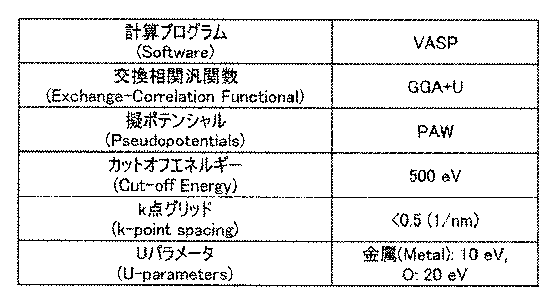


ここで、本発明の一態様の金属酸化物の形成に用いることができるALD法を利用した成膜装置(以下、ALD装置ともいう。)、およびALD法を用いた成膜方法について説明する。
CAAC−OSは、複数の結晶領域を有し、当該複数の結晶領域はc軸が特定の方向に配向している酸化物半導体である。なお、特定の方向とは、CAAC−OS膜の厚さ方向、CAAC−OS膜の被形成面の法線方向、またはCAAC−OS膜の表面の法線方向である。また、結晶領域とは、原子配列に周期性を有する領域である。なお、原子配列を格子配列とみなすと、結晶領域とは、格子配列の揃った領域でもある。さらに、CAAC−OSは、a−b面方向において複数の結晶領域が連結する領域を有し、当該領域は歪みを有する場合がある。なお、歪みとは、複数の結晶領域が連結する領域において、格子配列の揃った領域と、別の格子配列の揃った領域と、の間で格子配列の向きが変化している箇所を指す。つまり、CAAC−OSは、c軸配向し、a−b面方向には明らかな配向をしていない酸化物半導体である。
続いて、上記酸化物半導体をトランジスタに用いる場合について説明する。
ここで、酸化物半導体中における各不純物の影響について説明する。
成膜装置4000は、搬入搬出室4002と、搬入搬出室4004と、搬送室4006と、成膜室4008と、成膜室4009と、成膜室4010と、搬送アーム4014と、を有する。ここで、搬入搬出室4002、搬入搬出室4004、成膜室4008、成膜室4009、および成膜室4010は、搬送室4006とそれぞれ独立に接続されている。これにより、成膜室4008、成膜室4009、および成膜室4010において大気に曝すことなく、連続成膜を行うことができ、膜中に不純物が混入するのを防ぐことができる。また、基板と膜の界面、および各膜の界面の汚染は低減され、清浄な界面が得られる。
次に、成膜装置4000に用いることができるALD装置の構成について、図18Bを用いて説明する。ALD装置は、成膜室(チャンバー4020)と、原料供給部4021(原料供給部4021a、および原料供給部4021b)と、原料供給部4031と、導入量制御器である高速バルブ4022a、および高速バルブ4022bと、原料導入口4023(原料導入口4023a、および原料導入口4023b)と、原料導入口4033と、原料排出口4024と、排気装置4025とを有する。チャンバー4020内に設置される原料導入口4023a、原料導入口4023b、および原料導入口4033は供給管やバルブを介して原料供給部4021a、原料供給部4021b、および原料供給部4031とそれぞれ接続されており、原料排出口4024は、排出管やバルブや圧力調整器を介して排気装置4025と接続されている。
図20Aに、図18Bに示すALD装置を用いた成膜シーケンスを示す。まず、チャンバー4020内の基板ホルダ4026に基板4030をセットする(ステップS101)。次に、ヒータ4027の温度調節を行う(ステップS102)。次に、基板4030の温度が基板面内で一様になるように、基板4030を基板ホルダ4026上で保持する(ステップS103)。次に、前述の第1ステップ乃至第4ステップにより、成膜を行う。すなわち、チャンバー4020に第1の原料ガス、および第2の原料ガスを交互に導入し、基板4030上に成膜を行う(ステップS104)。また、ステップS103とステップS104の間に、チャンバー4020内部を酸素雰囲気にする処理を行ってもよい。基板4030のセット、および保持後に、チャンバー4020内部を酸素雰囲気とすることで、基板4030、および基板4030上に設けられた膜に酸素を添加できる場合がある。また、成膜前の基板4030、および基板4030上に設けられた膜から水素を脱離できる場合がある。基板4030中、または膜中の水素が、基板4030中、または膜中に添加された酸素と反応し、水(H2O)となって基板4030、または膜から離脱する場合がある。
本実施の形態では、図21A乃至図44Bを用いて、先の実施の形態で説明した金属酸化物を有するトランジスタを含む半導体装置の一例、およびその作製方法について説明する。
図21A乃至図21Dを用いて、先の実施の形態で説明した金属酸化物を有するトランジスタ200を含む半導体装置の構成を説明する。図21A乃至図21Dは、トランジスタ200を含む半導体装置の上面図および断面図である。図21Aは、当該半導体装置の上面図である。また、図21B乃至図21Dは、当該半導体装置の断面図である。ここで、図21Bは、図21AにA1−A2の一点鎖線で示す部位の断面図であり、トランジスタ200のチャネル長方向の断面図でもある。また、図21Cは、図21AにA3−A4の一点鎖線で示す部位の断面図であり、トランジスタ200のチャネル幅方向の断面図でもある。また、図21Dは、図21AにA5−A6の一点鎖線で示す部位の断面図である。なお、図21Aの上面図では、図の明瞭化のために一部の要素を省いている。
図21A乃至図21Dに示すように、トランジスタ200は、絶縁体214上の絶縁体216と、絶縁体214および/または絶縁体216に埋め込まれるように配置された導電体205(導電体205a、および導電体205b)と、絶縁体216上、および導電体205上の絶縁体222と、絶縁体222上の絶縁体224と、絶縁体224上の酸化物230aと、酸化物230a上の酸化物230bと、酸化物230b上の、酸化物243a、酸化物243b、および酸化物230cと、酸化物243a上の導電体242aと、酸化物243b上の導電体242bと、酸化物230c上の酸化物230dと、酸化物230d上の絶縁体250と、絶縁体250上に位置し、酸化物230cの一部と重なる導電体260(導電体260a、および導電体260b)と、絶縁体224の上面、酸化物230aの側面、酸化物230bの側面、導電体242aの側面、導電体242aの上面、導電体242bの側面、および導電体242bの上面と接する絶縁体254と、を有する。また、酸化物230cは、酸化物243aの側面、酸化物243bの側面、導電体242aの側面、および導電体242bの側面と接する。また、絶縁体282は、導電体260、絶縁体250、酸化物230d、酸化物230c、および絶縁体280のそれぞれの上面と接する。
本項では、金属酸化物における、酸素欠損中の水素の拡散または酸素欠損からの脱離について、計算を用いて評価する。具体的には、第一原理分子動力学計算、および、化学反応経路探索手法を援用した第一原理計算を用いる。
ここでは、第一原理分子動力学計算に用いる計算モデルについて説明する。
次に、第一原理分子動力学計算の計算条件について説明する。

第一原理分子動力学計算中の水素の軌跡を、図23A乃至図23Fに示す。図23A乃至図23Cは、VOH欠陥を含むc−IGZOモデルでの、第一原理分子動力学計算中の水素の軌跡を示す図である。また、図23D乃至図23Fは、VOH欠陥を含むa−IGZOモデルでの、第一原理分子動力学計算中の水素の軌跡を示す図である。なお、図23A、および図23Dは、温度を600℃に設定したときの、第一原理分子動力学計算中の水素の軌跡を示す図である。また、図23B、および図23Eは、温度を800℃に設定したときの、第一原理分子動力学計算中の水素の軌跡を示す図である。また、図23C、および図23Fは、温度を1000℃に設定したときの、第一原理分子動力学計算中の水素の軌跡を示す図である。
次に、化学反応経路探索手法を援用した第一原理計算に用いる計算モデルについて説明する。
次に、化学反応経路探索手法を援用した第一原理計算の計算条件について説明する。
NEB法を援用した計算で得られた、酸素欠損中の水素が酸素欠損から脱離する過程における、エネルギーの推移を、図25Aおよび図25Bに示す。図25Aは、VOH欠陥を含むc−IGZOモデルの経路C(図24参照)における、エネルギーの推移を示す図である。また、図25Bは、VOH欠陥を含むa−IGZOモデルでの、ある経路における、エネルギーの推移を示す図である。図25A、および図25Bにおいて、横軸は反応座標であり、縦軸はエネルギー(eV)である。
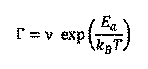

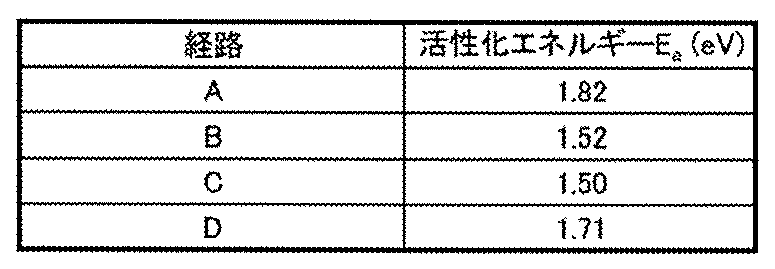
以下では、半導体装置に用いることができる構成材料について説明する。
トランジスタ200を形成する基板としては、例えば、絶縁体基板、半導体基板、または導電体基板を用いればよい。絶縁体基板としては、例えば、ガラス基板、石英基板、サファイア基板、安定化ジルコニア基板(イットリア安定化ジルコニア基板など)、樹脂基板などがある。また、半導体基板としては、例えば、シリコン、ゲルマニウムを材料とした半導体基板、または炭化シリコン、シリコンゲルマニウム、ヒ化ガリウム、リン化インジウム、酸化亜鉛、酸化ガリウムからなる化合物半導体基板などがある。さらには、前述の半導体基板内部に絶縁体領域を有する半導体基板、例えば、SOI(Silicon On Insulator)基板などがある。導電体基板としては、黒鉛基板、金属基板、合金基板、導電性樹脂基板などがある。または、金属の窒化物を有する基板、金属の酸化物を有する基板などがある。さらには、絶縁体基板に導電体または半導体が設けられた基板、半導体基板に導電体または絶縁体が設けられた基板、導電体基板に半導体または絶縁体が設けられた基板などがある。または、これらの基板に素子が設けられたものを用いてもよい。基板に設けられる素子としては、容量素子、抵抗素子、スイッチ素子、発光素子、記憶素子などがある。
絶縁体としては、絶縁性を有する酸化物、窒化物、酸化窒化物、窒化酸化物、金属酸化物、金属酸化窒化物、金属窒化酸化物などがある。
導電体としては、アルミニウム、クロム、銅、銀、金、白金、タンタル、ニッケル、チタン、モリブデン、タングステン、ハフニウム、バナジウム、ニオブ、マンガン、マグネシウム、ジルコニウム、ベリリウム、インジウム、ルテニウム、イリジウム、ストロンチウム、ランタンなどから選ばれた金属元素、または上述した金属元素を成分とする合金か、上述した金属元素を組み合わせた合金等を用いることが好ましい。例えば、窒化タンタル、窒化チタン、タングステン、チタンとアルミニウムを含む窒化物、タンタルとアルミニウムを含む窒化物、酸化ルテニウム、窒化ルテニウム、ストロンチウムとルテニウムを含む酸化物、ランタンとニッケルを含む酸化物などを用いることが好ましい。また、窒化タンタル、窒化チタン、チタンとアルミニウムを含む窒化物、タンタルとアルミニウムを含む窒化物、酸化ルテニウム、窒化ルテニウム、ストロンチウムとルテニウムを含む酸化物、ランタンとニッケルを含む酸化物は、酸化しにくい導電性材料、または、酸素を吸収しても導電性を維持する材料であるため、好ましい。また、リン等の不純物元素を含有させた多結晶シリコンに代表される、電気伝導度が高い半導体、ニッケルシリサイドなどのシリサイドを用いてもよい。
以下では、図29A乃至図29Dを用いて、本発明の一態様である半導体装置の一例について説明する。
図29A乃至図29Dに示す半導体装置は、図21A乃至図21Dに示した半導体装置の変形例である。図29A乃至図29Dに示す半導体装置は、図21A乃至図21Dに示した半導体装置とは、絶縁体283の形状が異なる。また、絶縁体287、および絶縁体274を有することが異なる。また、絶縁体284を有さないことが異なる。
次に、図29A乃至図29Dに示す、本発明の一態様である半導体装置の作製方法を、図30A乃至図42Dを用いて説明する。
以下では、図43A乃至図43Dを用いて、本実施の形態における半導体装置の一例について説明する。
以下では、図44Aおよび図44Bを用いて、先の<半導体装置の構成例>および先の<半導体装置の変形例>で示したものとは異なる、本発明の一態様に係るトランジスタ200を有する半導体装置の一例について説明する。なお、図44Aおよび図44Bに示す半導体装置において、<半導体装置の変形例>に示した半導体装置(図29A乃至図29D参照。)を構成する構造と同機能を有する構造には、同符号を付記する。なお、本項目において、トランジスタ200の構成材料については<半導体装置の構成例>および<半導体装置の変形例>で詳細に説明した材料を用いることができる。
本実施の形態では、半導体装置の一形態を、図45および図46を用いて説明する。
本発明の一態様に係る半導体装置(記憶装置)の一例を図45に示す。本発明の一態様の半導体装置では、トランジスタ200はトランジスタ300の上方に設けられ、容量素子100はトランジスタ300、およびトランジスタ200の上方に設けられている。なお、トランジスタ200として、先の実施の形態で説明したトランジスタ200を用いることができる。
トランジスタ300は、基板311上に設けられ、ゲートとして機能する導電体316、ゲート絶縁体として機能する絶縁体315、基板311の一部からなる半導体領域313、およびソース領域またはドレイン領域として機能する低抵抗領域314a、および低抵抗領域314bを有する。トランジスタ300は、pチャネル型、あるいはnチャネル型のいずれでもよい。
容量素子100は、トランジスタ200の上方に設けられる。容量素子100は、第1の電極として機能する導電体110と、第2の電極として機能する導電体120と、誘電体として機能する絶縁体130とを有する。ここで、絶縁体130は、上記実施の形態に示す絶縁体286として用いることができる絶縁体を用いることが好ましい。
各構造体の間には、層間膜、配線、およびプラグ等が設けられた配線層が設けられていてもよい。また、配線層は、設計に応じて複数層設けることができる。ここで、プラグまたは配線としての機能を有する導電体は、複数の構造をまとめて同一の符号を付与する場合がある。また、本明細書等において、配線と、配線と電気的に接続するプラグとが一体物であってもよい。すなわち、導電体の一部が配線として機能する場合、および導電体の一部がプラグとして機能する場合もある。
なお、トランジスタ200に、酸化物半導体を用いる場合、酸化物半導体の近傍に過剰酸素領域を有する絶縁体が設けることがある。その場合、該過剰酸素領域を有する絶縁体と、該過剰酸素領域を有する絶縁体に設ける導電体との間に、バリア性を有する絶縁体を設けることが好ましい。
以下では、大面積基板を半導体素子ごとに分断することによって、複数の半導体装置をチップ状で取り出す場合に設けられるダイシングライン(スクライブライン、分断ライン、又は切断ラインと呼ぶ場合がある)について説明する。分断方法としては、例えば、まず、基板に半導体素子を分断するための溝(ダイシングライン)を形成した後、ダイシングラインにおいて切断し、複数の半導体装置に分断(分割)する場合がある。
本実施の形態では、図47A、図47Bおよび図48A乃至図48Hを用いて、本発明の一態様に係る、酸化物を半導体に用いたトランジスタ(以下、OSトランジスタと呼ぶ場合がある。)、および容量素子が適用されている記憶装置(以下、OSメモリ装置と呼ぶ場合がある。)について説明する。OSメモリ装置は、少なくとも容量素子と、容量素子の充放電を制御するOSトランジスタを有する記憶装置である。OSトランジスタのオフ電流は極めて小さいので、OSメモリ装置は優れた保持特性をもち、不揮発性メモリとして機能させることができる。
図47AにOSメモリ装置の構成の一例を示す。記憶装置1400は、周辺回路1411、およびメモリセルアレイ1470を有する。周辺回路1411は、行回路1420、列回路1430、出力回路1440、およびコントロールロジック回路1460を有する。
図48A乃至図48Cに、DRAMのメモリセルの回路構成例を示す。本明細書等において、1OSトランジスタ1容量素子型のメモリセルを用いたDRAMを、DOSRAM(Dynamic Oxide Semiconductor Random Access Memory)と呼ぶ場合がある。図48Aに示す、メモリセル1471は、トランジスタM1と、容量素子CAと、を有する。なお、トランジスタM1は、ゲート(トップゲートと呼ぶ場合がある。)、及びバックゲートを有する。
図48D乃至図48Gに、2トランジスタ1容量素子のゲインセル型のメモリセルの回路構成例を示す。図48Dに示す、メモリセル1474は、トランジスタM2と、トランジスタM3と、容量素子CBと、を有する。なお、トランジスタM2は、トップゲート(単にゲートと呼ぶ場合がある。)、及びバックゲートを有する。本明細書等において、トランジスタM2にOSトランジスタを用いたゲインセル型のメモリセルを有する記憶装置を、NOSRAM(Nonvolatile Oxide Semiconductor RAM)と呼ぶ場合がある。
本実施の形態では、図49Aおよび図49Bを用いて、本発明の半導体装置が実装されたチップ1200の一例を示す。チップ1200には、複数の回路(システム)が実装されている。このように、複数の回路(システム)を一つのチップに集積する技術を、システムオンチップ(System on Chip:SoC)と呼ぶ場合がある。
本実施の形態は、上記実施の形態に示す記憶装置などが組み込まれた電子部品および電子機器の一例を示す。
まず、記憶装置720が組み込まれた電子部品の例を、図50Aおよび図50Bを用いて説明を行う。
本実施の形態では、先の実施の形態に示す半導体装置を用いた記憶装置の応用例について説明する。先の実施の形態に示す半導体装置は、例えば、各種電子機器(例えば、情報端末、コンピュータ、スマートフォン、電子書籍端末、デジタルカメラ(ビデオカメラも含む)、録画再生装置、ナビゲーションシステムなど)の記憶装置に適用できる。なお、ここで、コンピュータとは、タブレット型のコンピュータ、ノート型のコンピュータ、デスクトップ型のコンピュータの他、サーバシステムのような大型のコンピュータを含むものである。または、先の実施の形態に示す半導体装置は、メモリカード(例えば、SDカード)、USBメモリ、SSD(ソリッド・ステート・ドライブ)等の各種のリムーバブル記憶装置に適用される。図51A乃至図51Eにリムーバブル記憶装置の幾つかの構成例を模式的に示す。例えば、先の実施の形態に示す半導体装置は、パッケージングされたメモリチップに加工され、様々なストレージ装置、リムーバブルメモリに用いられる。
本発明の一態様に係る半導体装置は、CPUやGPUなどのプロセッサ、またはチップに用いることができる。図52A乃至図52Hに、本発明の一態様に係るCPUやGPUなどのプロセッサ、またはチップを備えた電子機器の具体例を示す。
本発明の一態様に係るGPUまたはチップは、様々な電子機器に搭載することができる。電子機器の例としては、例えば、テレビジョン装置、デスクトップ型またはノート型の情報端末用などのモニタ、デジタルサイネージ(Digital Signage:電子看板)、パチンコ機などの大型ゲーム機、などの比較的大きな画面を備える電子機器の他、デジタルカメラ、デジタルビデオカメラ、デジタルフォトフレーム、電子ブックリーダー、携帯電話機、携帯型ゲーム機、携帯情報端末、音響再生装置、などが挙げられる。また、本発明の一態様に係るGPUまたはチップを電子機器に設けることにより、電子機器に人工知能を搭載することができる。
図52Aには、情報端末の一種である携帯電話(スマートフォン)が図示されている。情報端末5100は、筐体5101と、表示部5102と、を有しており、入力用インターフェースとして、タッチパネルが表示部5102に備えられ、ボタンが筐体5101に備えられている。
図52Cは、ゲーム機の一例である携帯ゲーム機5300を示している。携帯ゲーム機5300は、筐体5301、筐体5302、筐体5303、表示部5304、接続部5305、操作キー5306等を有する。筐体5302、および筐体5303は、筐体5301から取り外すことが可能である。筐体5301に設けられている接続部5305を別の筐体(図示せず)に取り付けることで、表示部5304に出力される映像を、別の映像機器(図示せず)に出力することができる。このとき、筐体5302、および筐体5303は、それぞれ操作部として機能することができる。これにより、複数のプレイヤーが同時にゲームを行うことができる。筐体5301、筐体5302、および筐体5303の基板に設けられているチップなどに先の実施の形態に示すチップを組み込むことができる。
本発明の一態様のGPUまたはチップは、大型コンピュータに適用することができる。
本発明の一態様のGPUまたはチップは、移動体である自動車、および自動車の運転席周辺に適用することができる。
図52Hは、電化製品の一例である電気冷凍冷蔵庫5800を示している。電気冷凍冷蔵庫5800は、筐体5801、冷蔵室用扉5802、冷凍室用扉5803等を有する。
Claims (5)
- 結晶を有する金属酸化物であって、
前記結晶は、第1の層と、第2の層と、第3の層と、が積層された構造を有し、
前記第1の層、前記第2の層、および前記第3の層は、それぞれ前記金属酸化物の被形成面と概略平行であり、
前記第1の層は、第1の金属と、酸素と、を有し、
前記第2の層は、第2の金属と、酸素と、を有し、
前記第3の層は、第3の金属と、酸素と、を有し、
前記第1の層は、八面体形構造を有し、
前記第2の層は、三方両錐形構造または四面体形構造を有し、
前記第3の層は、三方両錐形構造または四面体形構造を有し、
前記第1の層が有する、前記八面体形構造は、中心に前記第1の金属の原子が存在し、頂点に酸素の原子が存在し、
前記第2の層が有する、前記三方両錐形構造または前記四面体形構造は、中心に前記第2の金属の原子が存在し、頂点に酸素の原子が存在し、
前記第3の層が有する、前記三方両錐形構造または前記四面体形構造は、中心に前記第3の金属の原子が存在し、頂点に酸素の原子が存在し、
前記第1の金属の価数は、前記第2の金属の価数と同じであり、
前記第1の金属の価数は、前記第3の金属の価数と異なる、
金属酸化物。 - 結晶を有する金属酸化物であって、
前記結晶は、第1の層と、第2の層と、第3の層と、が積層された構造を有し、
前記第1の層、前記第2の層、および前記第3の層は、それぞれ前記金属酸化物の被形成面と概略平行であり、
前記第1の層、前記第2の層のそれぞれは、第1の金属と、第2の金属と、酸素と、を有し、
前記第3の層は、第3の金属と、酸素と、を有し、
前記第1の層は、八面体形構造を有し、
前記第2の層は、三方両錐形構造または四面体形構造を有し、
前記第3の層は、三方両錐形構造または四面体形構造を有し、
前記第1の層が有する、前記八面体形構造は、中心に前記第1の金属または前記第2の金属の原子が存在し、頂点に酸素の原子が存在し、
前記第2の層が有する、前記三方両錐形構造または前記四面体形構造は、中心に前記第1の金属の原子または前記第2の金属の原子が存在し、頂点に酸素の原子が存在し、
前記第3の層が有する、前記三方両錐形構造または前記四面体形構造は、中心に前記第3の金属の原子が存在し、頂点に酸素の原子が存在し、
前記第1の金属の価数は、前記第2の金属の価数と同じであり、
前記第1の金属の価数は、前記第3の金属の価数と異なる、
金属酸化物。 - 請求項1または請求項2において、
前記結晶は、YbFe2O4型構造、または、Yb2Fe3O7型構造を有する、
金属酸化物。 - 請求項1乃至請求項3のいずれか一において、
前記第1の金属は、インジウムであり、
前記第2の金属は、ガリウムであり、
前記第3の金属は、亜鉛である、
金属酸化物。 - 請求項1乃至請求項4のいずれか一項に記載の金属酸化物を、チャネル形成領域に有する、
トランジスタ。
Priority Applications (5)
| Application Number | Priority Date | Filing Date | Title |
|---|---|---|---|
| JP2021525401A JPWO2020250079A5 (ja) | 2020-06-01 | 金属酸化物およびトランジスタ | |
| US17/616,426 US20220238718A1 (en) | 2019-06-12 | 2020-06-01 | Metal oxide and transistor including metal oxide |
| CN202080041170.8A CN113906570A (zh) | 2019-06-12 | 2020-06-01 | 金属氧化物以及包含金属氧化物的晶体管 |
| KR1020217041266A KR20220020829A (ko) | 2019-06-12 | 2020-06-01 | 금속 산화물, 및 금속 산화물을 가지는 트랜지스터 |
| JP2025146899A JP2025179177A (ja) | 2019-06-12 | 2025-09-04 | 金属酸化物 |
Applications Claiming Priority (8)
| Application Number | Priority Date | Filing Date | Title |
|---|---|---|---|
| JP2019-109490 | 2019-06-12 | ||
| JP2019109490 | 2019-06-12 | ||
| JP2019123682 | 2019-07-02 | ||
| JP2019-123682 | 2019-07-02 | ||
| JP2019-157820 | 2019-08-30 | ||
| JP2019157820 | 2019-08-30 | ||
| JP2019194248 | 2019-10-25 | ||
| JP2019-194248 | 2019-10-25 |
Publications (1)
| Publication Number | Publication Date |
|---|---|
| WO2020250079A1 true WO2020250079A1 (ja) | 2020-12-17 |
Family
ID=73781876
Family Applications (1)
| Application Number | Title | Priority Date | Filing Date |
|---|---|---|---|
| PCT/IB2020/055157 Ceased WO2020250079A1 (ja) | 2019-06-12 | 2020-06-01 | 金属酸化物、および金属酸化物を有するトランジスタ |
Country Status (5)
| Country | Link |
|---|---|
| US (1) | US20220238718A1 (ja) |
| JP (1) | JP2025179177A (ja) |
| KR (1) | KR20220020829A (ja) |
| CN (1) | CN113906570A (ja) |
| WO (1) | WO2020250079A1 (ja) |
Families Citing this family (2)
| Publication number | Priority date | Publication date | Assignee | Title |
|---|---|---|---|---|
| JP7352058B2 (ja) * | 2017-11-01 | 2023-09-28 | セントラル硝子株式会社 | 炭化ケイ素単結晶の製造方法 |
| WO2025184829A1 (zh) * | 2024-03-06 | 2025-09-12 | 华南理工大学 | 一种半导体氧化物薄膜及其制备方法 |
Citations (4)
| Publication number | Priority date | Publication date | Assignee | Title |
|---|---|---|---|---|
| JP2012134467A (ja) * | 2010-11-30 | 2012-07-12 | Semiconductor Energy Lab Co Ltd | 半導体装置の作製方法 |
| JP2014194076A (ja) * | 2013-02-28 | 2014-10-09 | Semiconductor Energy Lab Co Ltd | スパッタリングターゲットの製造方法、酸化物膜の成膜方法、及びトランジスタ |
| JP2018116274A (ja) * | 2017-01-16 | 2018-07-26 | 株式会社半導体エネルギー研究所 | 表示装置 |
| JP2018180436A (ja) * | 2017-04-20 | 2018-11-15 | 株式会社半導体エネルギー研究所 | 表示装置 |
Family Cites Families (2)
| Publication number | Priority date | Publication date | Assignee | Title |
|---|---|---|---|---|
| SG11201503709SA (en) * | 2011-05-13 | 2015-07-30 | Semiconductor Energy Lab | Semiconductor device |
| US9762246B2 (en) * | 2011-05-20 | 2017-09-12 | Semiconductor Energy Laboratory Co., Ltd. | Semiconductor device with a storage circuit having an oxide semiconductor |
-
2020
- 2020-06-01 KR KR1020217041266A patent/KR20220020829A/ko active Pending
- 2020-06-01 WO PCT/IB2020/055157 patent/WO2020250079A1/ja not_active Ceased
- 2020-06-01 US US17/616,426 patent/US20220238718A1/en active Pending
- 2020-06-01 CN CN202080041170.8A patent/CN113906570A/zh active Pending
-
2025
- 2025-09-04 JP JP2025146899A patent/JP2025179177A/ja active Pending
Patent Citations (4)
| Publication number | Priority date | Publication date | Assignee | Title |
|---|---|---|---|---|
| JP2012134467A (ja) * | 2010-11-30 | 2012-07-12 | Semiconductor Energy Lab Co Ltd | 半導体装置の作製方法 |
| JP2014194076A (ja) * | 2013-02-28 | 2014-10-09 | Semiconductor Energy Lab Co Ltd | スパッタリングターゲットの製造方法、酸化物膜の成膜方法、及びトランジスタ |
| JP2018116274A (ja) * | 2017-01-16 | 2018-07-26 | 株式会社半導体エネルギー研究所 | 表示装置 |
| JP2018180436A (ja) * | 2017-04-20 | 2018-11-15 | 株式会社半導体エネルギー研究所 | 表示装置 |
Non-Patent Citations (1)
| Title |
|---|
| KIMIZUKA, NOBORU, SIRATORI, KIITI: "YbFe2O4 Type of Compounds with a Layered Structure", NIHON KESSHO GAKKAISHI, vol. 26, no. 6, 1984, pages 334 - 342 * |
Also Published As
| Publication number | Publication date |
|---|---|
| CN113906570A (zh) | 2022-01-07 |
| US20220238718A1 (en) | 2022-07-28 |
| JP2025179177A (ja) | 2025-12-09 |
| KR20220020829A (ko) | 2022-02-21 |
| JPWO2020250079A1 (ja) | 2020-12-17 |
Similar Documents
| Publication | Publication Date | Title |
|---|---|---|
| JP7678789B2 (ja) | 金属酸化物の成膜方法 | |
| JPWO2019234561A1 (ja) | 半導体装置、および半導体装置の作製方法 | |
| KR102959193B1 (ko) | 반도체 장치 및 반도체 장치의 제작 방법 | |
| JP7640472B2 (ja) | 半導体装置、および半導体装置の作製方法 | |
| WO2021019334A1 (ja) | 半導体装置 | |
| WO2020201870A1 (ja) | 半導体装置、および半導体装置の作製方法 | |
| WO2020201873A1 (ja) | 半導体装置の作製方法 | |
| WO2021009620A1 (ja) | 半導体装置、および半導体装置の作製方法 | |
| JP7808724B2 (ja) | 半導体装置の作製方法 | |
| JP2025179177A (ja) | 金属酸化物 | |
| JP2025069295A (ja) | 半導体装置 | |
| JP2025075041A (ja) | 金属酸化物の形成方法 | |
| JP2025164843A (ja) | 記憶装置 | |
| WO2021084369A1 (ja) | 半導体装置 | |
| JP2026050481A (ja) | 半導体装置の作製方法 | |
| WO2020250083A1 (ja) | 半導体装置、および半導体装置の作製方法 | |
| WO2021090116A1 (ja) | 半導体装置およびその作製方法 | |
| JP2026020220A (ja) | 金属酸化物の製造方法 | |
| WO2022038453A1 (ja) | 絶縁膜の改質方法、および半導体装置の作製方法 | |
| US20220157992A1 (en) | A semiconductor device and a method for manufacturing the semiconductor device | |
| WO2022043809A1 (ja) | 半導体装置の作製方法 | |
| WO2021130600A1 (ja) | 半導体装置、半導体装置の作製方法 | |
| WO2021090115A1 (ja) | 半導体装置 | |
| JP2026020276A (ja) | 半導体装置の作製方法 | |
| WO2022038447A1 (ja) | 半導体装置の作製方法 |
Legal Events
| Date | Code | Title | Description |
|---|---|---|---|
| 121 | Ep: the epo has been informed by wipo that ep was designated in this application |
Ref document number: 20823267 Country of ref document: EP Kind code of ref document: A1 |
|
| ENP | Entry into the national phase |
Ref document number: 2021525401 Country of ref document: JP Kind code of ref document: A |
|
| NENP | Non-entry into the national phase |
Ref country code: DE |
|
| 122 | Ep: pct application non-entry in european phase |
Ref document number: 20823267 Country of ref document: EP Kind code of ref document: A1 |
|
| WWR | Wipo information: refused in national office |
Ref document number: 1020217041266 Country of ref document: KR |