WO2020246344A1 - 半導体記憶装置 - Google Patents
半導体記憶装置 Download PDFInfo
- Publication number
- WO2020246344A1 WO2020246344A1 PCT/JP2020/020975 JP2020020975W WO2020246344A1 WO 2020246344 A1 WO2020246344 A1 WO 2020246344A1 JP 2020020975 W JP2020020975 W JP 2020020975W WO 2020246344 A1 WO2020246344 A1 WO 2020246344A1
- Authority
- WO
- WIPO (PCT)
- Prior art keywords
- node
- transistors
- transistor
- dimensional structure
- gate
- Prior art date
- Legal status (The legal status is an assumption and is not a legal conclusion. Google has not performed a legal analysis and makes no representation as to the accuracy of the status listed.)
- Ceased
Links
Images











Classifications
-
- H—ELECTRICITY
- H10—SEMICONDUCTOR DEVICES; ELECTRIC SOLID-STATE DEVICES NOT OTHERWISE PROVIDED FOR
- H10B—ELECTRONIC MEMORY DEVICES
- H10B10/00—Static random access memory [SRAM] devices
- H10B10/12—Static random access memory [SRAM] devices comprising a MOSFET load element
- H10B10/125—Static random access memory [SRAM] devices comprising a MOSFET load element the MOSFET being a thin film transistor [TFT]
-
- H—ELECTRICITY
- H10—SEMICONDUCTOR DEVICES; ELECTRIC SOLID-STATE DEVICES NOT OTHERWISE PROVIDED FOR
- H10D—INORGANIC ELECTRIC SEMICONDUCTOR DEVICES
- H10D30/00—Field-effect transistors [FET]
- H10D30/40—FETs having zero-dimensional [0D], one-dimensional [1D] or two-dimensional [2D] charge carrier gas channels
- H10D30/43—FETs having zero-dimensional [0D], one-dimensional [1D] or two-dimensional [2D] charge carrier gas channels having one-dimensional [1D] charge carrier gas channels, e.g. quantum wire FETs or transistors having 1D quantum-confined channels
-
- H—ELECTRICITY
- H10—SEMICONDUCTOR DEVICES; ELECTRIC SOLID-STATE DEVICES NOT OTHERWISE PROVIDED FOR
- H10D—INORGANIC ELECTRIC SEMICONDUCTOR DEVICES
- H10D30/00—Field-effect transistors [FET]
- H10D30/60—Insulated-gate field-effect transistors [IGFET]
- H10D30/67—Thin-film transistors [TFT]
- H10D30/6729—Thin-film transistors [TFT] characterised by the electrodes
- H10D30/673—Thin-film transistors [TFT] characterised by the electrodes characterised by the shapes, relative sizes or dispositions of the gate electrodes
- H10D30/6735—Thin-film transistors [TFT] characterised by the electrodes characterised by the shapes, relative sizes or dispositions of the gate electrodes having gates fully surrounding the channels, e.g. gate-all-around
-
- H—ELECTRICITY
- H10—SEMICONDUCTOR DEVICES; ELECTRIC SOLID-STATE DEVICES NOT OTHERWISE PROVIDED FOR
- H10D—INORGANIC ELECTRIC SEMICONDUCTOR DEVICES
- H10D30/00—Field-effect transistors [FET]
- H10D30/60—Insulated-gate field-effect transistors [IGFET]
- H10D30/67—Thin-film transistors [TFT]
- H10D30/6757—Thin-film transistors [TFT] characterised by the structure of the channel, e.g. transverse or longitudinal shape or doping profile
-
- H—ELECTRICITY
- H10—SEMICONDUCTOR DEVICES; ELECTRIC SOLID-STATE DEVICES NOT OTHERWISE PROVIDED FOR
- H10D—INORGANIC ELECTRIC SEMICONDUCTOR DEVICES
- H10D62/00—Semiconductor bodies, or regions thereof, of devices having potential barriers
- H10D62/10—Shapes, relative sizes or dispositions of the regions of the semiconductor bodies; Shapes of the semiconductor bodies
- H10D62/117—Shapes of semiconductor bodies
- H10D62/118—Nanostructure semiconductor bodies
- H10D62/119—Nanowire, nanosheet or nanotube semiconductor bodies
- H10D62/121—Nanowire, nanosheet or nanotube semiconductor bodies oriented parallel to substrates
-
- H—ELECTRICITY
- H10—SEMICONDUCTOR DEVICES; ELECTRIC SOLID-STATE DEVICES NOT OTHERWISE PROVIDED FOR
- H10D—INORGANIC ELECTRIC SEMICONDUCTOR DEVICES
- H10D89/00—Aspects of integrated devices not covered by groups H10D84/00 - H10D88/00
- H10D89/10—Integrated device layouts
-
- B—PERFORMING OPERATIONS; TRANSPORTING
- B82—NANOTECHNOLOGY
- B82Y—SPECIFIC USES OR APPLICATIONS OF NANOSTRUCTURES; MEASUREMENT OR ANALYSIS OF NANOSTRUCTURES; MANUFACTURE OR TREATMENT OF NANOSTRUCTURES
- B82Y10/00—Nanotechnology for information processing, storage or transmission, e.g. quantum computing or single electron logic
-
- G—PHYSICS
- G11—INFORMATION STORAGE
- G11C—STATIC STORES
- G11C11/00—Digital stores characterised by the use of particular electric or magnetic storage elements; Storage elements therefor
- G11C11/21—Digital stores characterised by the use of particular electric or magnetic storage elements; Storage elements therefor using electric elements
- G11C11/34—Digital stores characterised by the use of particular electric or magnetic storage elements; Storage elements therefor using electric elements using semiconductor devices
- G11C11/40—Digital stores characterised by the use of particular electric or magnetic storage elements; Storage elements therefor using electric elements using semiconductor devices using transistors
- G11C11/41—Digital stores characterised by the use of particular electric or magnetic storage elements; Storage elements therefor using electric elements using semiconductor devices using transistors forming static cells with positive feedback, i.e. cells not needing refreshing or charge regeneration, e.g. bistable multivibrator or Schmitt trigger
- G11C11/412—Digital stores characterised by the use of particular electric or magnetic storage elements; Storage elements therefor using electric elements using semiconductor devices using transistors forming static cells with positive feedback, i.e. cells not needing refreshing or charge regeneration, e.g. bistable multivibrator or Schmitt trigger using field-effect transistors only
-
- G—PHYSICS
- G11—INFORMATION STORAGE
- G11C—STATIC STORES
- G11C8/00—Arrangements for selecting an address in a digital store
- G11C8/16—Multiple access memory array, e.g. addressing one storage element via at least two independent addressing line groups
-
- H—ELECTRICITY
- H10—SEMICONDUCTOR DEVICES; ELECTRIC SOLID-STATE DEVICES NOT OTHERWISE PROVIDED FOR
- H10D—INORGANIC ELECTRIC SEMICONDUCTOR DEVICES
- H10D62/00—Semiconductor bodies, or regions thereof, of devices having potential barriers
- H10D62/80—Semiconductor bodies, or regions thereof, of devices having potential barriers characterised by the materials
- H10D62/82—Heterojunctions
- H10D62/822—Heterojunctions comprising only Group IV materials heterojunctions, e.g. Si/Ge heterojunctions
-
- H—ELECTRICITY
- H10—SEMICONDUCTOR DEVICES; ELECTRIC SOLID-STATE DEVICES NOT OTHERWISE PROVIDED FOR
- H10D—INORGANIC ELECTRIC SEMICONDUCTOR DEVICES
- H10D84/00—Integrated devices formed in or on semiconductor substrates that comprise only semiconducting layers, e.g. on Si wafers or on GaAs-on-Si wafers
- H10D84/80—Integrated devices formed in or on semiconductor substrates that comprise only semiconducting layers, e.g. on Si wafers or on GaAs-on-Si wafers characterised by the integration of at least one component covered by groups H10D12/00 or H10D30/00, e.g. integration of IGFETs
- H10D84/82—Integrated devices formed in or on semiconductor substrates that comprise only semiconducting layers, e.g. on Si wafers or on GaAs-on-Si wafers characterised by the integration of at least one component covered by groups H10D12/00 or H10D30/00, e.g. integration of IGFETs of only field-effect components
- H10D84/83—Integrated devices formed in or on semiconductor substrates that comprise only semiconducting layers, e.g. on Si wafers or on GaAs-on-Si wafers characterised by the integration of at least one component covered by groups H10D12/00 or H10D30/00, e.g. integration of IGFETs of only field-effect components of only insulated-gate FETs [IGFET]
- H10D84/85—Complementary IGFETs, e.g. CMOS
-
- H—ELECTRICITY
- H10—SEMICONDUCTOR DEVICES; ELECTRIC SOLID-STATE DEVICES NOT OTHERWISE PROVIDED FOR
- H10D—INORGANIC ELECTRIC SEMICONDUCTOR DEVICES
- H10D88/00—Three-dimensional [3D] integrated devices
Definitions
- the present disclosure relates to a semiconductor storage device including a three-dimensional structure transistor, and particularly to a layout structure of a 2-port SRAM (Static Random Access Memory) cell using a three-dimensional structure transistor.
- a 2-port SRAM Static Random Access Memory
- SRAM is widely used in semiconductor integrated circuits.
- a SRAM a 2-port SRAM provided with two ports for reading and writing data is known (for example, Patent Document 1).
- the transistor which is a basic component of LSI, has realized improvement of integration degree, reduction of operating voltage, and improvement of operating speed by reducing (scaling) the gate length.
- off-current due to excessive scaling and the resulting significant increase in power consumption have become problems.
- three-dimensional structure transistors in which the transistor structure is changed from the conventional planar type to the three-dimensional type are being actively studied.
- Non-Patent Documents 1 and 2 as new devices, a three-dimensional structure device in which a P-type FET and an N-type FET having a three-dimensional structure are laminated in a direction perpendicular to a substrate, and an SRAM cell using the same (hereinafter, simply referred to as a cell). Is disclosed.
- a three-dimensional structure device in which a three-dimensional structure P-type FET and an N-type FET are laminated in a direction perpendicular to a substrate is referred to as a CFET (Complementary FET), following the description of Non-Patent Document 1. To do. Further, the direction perpendicular to the substrate is called the depth direction.
- CFET Complementary FET
- a semiconductor storage device including a 2-port SRAM cell, in which one node supplies a first voltage to a first power source and the other node is a first node.
- a first transistor having a gate connected to a second node, one node connected to the first power supply, the other node connected to the second node, and a second node connected to the first node.
- a transistor, a third transistor having a gate connected to the first node, a second power supply to which one node supplies a second voltage different from the first voltage, and a third transistor having a gate connected to the second node.
- a fourth transistor with one node connected to the second node, the other node connected to the second power supply, a gate connected to the first node, one node to the first bit line, and the other node to the first bit line.
- the first node has a fifth transistor whose gate is connected to the first word line, and one node has the second bit line forming the first bit line and the first complementary bit line pair, and the other node. Is connected to the second node, the gate is connected to the first word line, one node is connected to the third bit line, the other node is connected to the first node, and the gate is the second word line.
- the 7th transistor connected to the above, one node to the 4th bit line forming the 3rd bit line and the 2nd complementary bit line pair, the other node to the 2nd node, and the gate to the 2nd It includes an eighth transistor connected to each word line.
- the third and fourth transistors are a first three-dimensional structure transistor, which is a first conductive type three-dimensional structure transistor formed in the first layer, and the second layer formed in a second layer different from the first layer, respectively. It is composed of a second three-dimensional structure transistor, which is a first conductive type three-dimensional structure transistor.
- the first transistor is composed of a second conductive type three-dimensional structure transistor formed in the second layer, which is different from the first conductive type.
- the second transistor is composed of the second conductive type three-dimensional structure transistor formed in the first layer.
- the fifth to eighth transistors include the first conductive type three-dimensional structure transistor formed in at least one of the first and second layers, respectively.
- a 2-port SRAM circuit is configured by the 1st to 8th transistors. Further, the third and fourth transistors are composed of a first conductive type three-dimensional structure transistor formed in the first layer and a first conductive type three-dimensional structure transistor formed in the second layer, respectively.
- the first transistor is composed of a second conductive type three-dimensional structure transistor formed in the second layer.
- the second transistor is composed of a second conductive type three-dimensional structure transistor formed in the first layer.
- Each of the fifth to eighth transistors includes a first conductive type three-dimensional structure transistor formed in at least one of the first layer and the second layer. That is, the first to eighth transistors constituting the 2-port SRAM circuit are each composed of three-dimensional structure transistors.
- the semiconductor storage device includes a 2-port SRAM cell, in which one node supplies a first voltage to a first power source and the other node is a first node.
- a first transistor having a gate connected to a second node, one node connected to the first power supply, the other node connected to the second node, and a second node connected to the first node.
- a transistor, a third transistor having a gate connected to the first node, a second power supply to which one node supplies a second voltage different from the first voltage, and a third transistor having a gate connected to the second node.
- a fourth transistor with one node connected to the second node, the other node connected to the second power supply, a gate connected to the first node, one node to the first bit line, and the other node to the first bit line.
- the first node has a fifth transistor whose gate is connected to the first word line, and one node has the second bit line forming the first bit line and the first complementary bit line pair, and the other node. Is connected to the second node, the gate is connected to the first word line, one node is connected to the third bit line, the other node is connected to the first node, and the gate is the second word line.
- the 7th transistor connected to the above, one node to the 4th bit line forming the 3rd bit line and the 2nd complementary bit line pair, the other node to the 2nd node, and the gate to the 2nd It includes an eighth transistor connected to each word line.
- the third and fourth transistors are a first three-dimensional structure transistor, which is a first conductive type three-dimensional structure transistor formed in the first layer, and the second layer formed in a second layer different from the first layer, respectively. It is composed of a second three-dimensional structure transistor, which is a first conductive type three-dimensional structure transistor.
- the first and second transistors are each composed of a second conductive type three-dimensional structure transistor formed in the second layer, which is different from the first conductive type.
- the fifth to eighth transistors include the first conductive type three-dimensional structure transistor formed in at least one of the first and second layers, respectively.
- a 2-port SRAM circuit is configured by the 1st to 8th transistors. Further, the third and fourth transistors are composed of a first conductive type three-dimensional structure transistor formed in the first layer and a first conductive type three-dimensional structure transistor formed in the second layer, respectively. The first and second transistors are each composed of a second conductive three-dimensional structure transistor formed in the second layer. Each of the fifth to eighth transistors includes a first conductive type three-dimensional structure transistor formed in at least one of the first layer and the second layer. That is, the first to eighth transistors constituting the 2-port SRAM circuit are each composed of three-dimensional structure transistors. As a result, a 2-port SRAM cell using a CFET can be realized.
- the semiconductor storage device includes a 2-port SRAM cell, in which one node supplies a first voltage to a first power source and the other node is a first node.
- a first transistor having a gate connected to a second node, one node connected to the first power supply, the other node connected to the second node, and a second node connected to the first node.
- a fourth transistor with one node connected to the second node, the other node connected to the second power supply, a gate connected to the first node, one node to the first bit line, and the other node to the first bit line.
- the first node has a fifth transistor whose gate is connected to the first word line, and one node has the second bit line forming the first bit line and the first complementary bit line pair, and the other node. Is connected to the second node, the gate is connected to the first word line, one node is connected to the third bit line, the other node is connected to the first node, and the gate is the second word line.
- the 7th transistor connected to the above, one node to the 4th bit line forming the 3rd bit line and the 2nd complementary bit line pair, the other node to the 2nd node, and the gate to the 2nd It includes an eighth transistor connected to each word line.
- the third and fourth transistors are each composed of a plurality of first three-dimensional structure transistors, which are a plurality of first conductive type three-dimensional structure transistors formed in the first layer.
- the plurality of first three-dimensional structure transistors are formed side by side in a second direction perpendicular to the first direction, which is the direction in which the channel portions of the first to eighth transistors extend.
- the first and second transistors each include a second conductive type three-dimensional structure transistor different from the first conductive type formed in a second layer different from the first layer, and at least a part thereof is said to be the first. It overlaps with the 3rd and 4th transistors in plan view.
- the fifth to eighth transistors include the first conductive type three-dimensional structure transistor formed in at least one of the first and second layers, respectively.
- a 2-port SRAM circuit is configured by the 1st to 8th transistors.
- the third and fourth transistors are each composed of a plurality of first conductive three-dimensional structure transistors formed in the first layer and arranged side by side in the second direction.
- the first and second transistors are each composed of a second conductive three-dimensional structure transistor formed in the second layer.
- Each of the fifth to eighth transistors includes a first conductive type three-dimensional structure transistor formed in at least one of the first layer and the second layer. That is, the first to eighth transistors constituting the 2-port SRAM circuit are each composed of three-dimensional structure transistors.
- the first and second transistors overlaps with the third and fourth transistors in a plan view, respectively. That is, the first and second transistors are laminated with the third and fourth transistors, respectively. As a result, the area of the 2-port SRAM cell can be reduced.
- a 2-port SRAM cell using a CFET can be realized, and the area of the 2-port SRAM cell can be reduced.
- the semiconductor storage device includes the first and second two-port SRAM cells, and one of the first and second two-port SRAM cells has a first voltage, respectively.
- the first transistor to which the other node is connected to the first node and the gate to the second node to the first power supply to be supplied, one node to the first power supply, and the other node to the second node.
- the gate is connected to the second transistor whose gate is connected to the first node, and to the second power source where one node supplies the first node and the other node supplies a second voltage different from the first voltage.
- a seventh transistor with a node connected to the first node and a gate connected to the second word line, and one node to the fourth bit line forming the third bit line and the second complementary bit line pair, and the other.
- Node is provided with the second node
- the gate is provided with an eighth transistor connected to the second word line.
- the first and second two-port SRAM cells are arranged adjacent to a second direction perpendicular to the first direction, which is the direction in which the channel portion of the first to eighth transistors extends.
- the third and fourth transistors each include a first conductive three-dimensional structure transistor formed in the first layer, and the first transistor is a respective transistor.
- a second conductive type three-dimensional structure transistor different from the first conductive type formed in a second layer different from the first layer is included, and the second transistor is formed in at least one of the first and second layers, respectively.
- the second conductive type three-dimensional structure transistor formed is included, and the fifth to eighth transistors are the first conductive type three-dimensional structure transistors formed on at least one of the first and second layers, respectively. Including. At least a part of the fifth and seventh transistors in the first two-port SRAM cell overlaps with the sixth and eighth transistors in the second two-port SRAM cell in a plan view, respectively.
- the first to eighth transistors provided in the first and second two-port SRAM cells respectively constitute a two-port SRAM circuit in the first and second two-port SRAM cells, respectively.
- the third and fourth transistors each include a first conductive type three-dimensional structure transistor formed in the first layer.
- Each of the first transistors includes a second conductive type three-dimensional structure transistor formed in the second layer.
- the second transistor includes a second conductive three-dimensional structure transistor formed on at least one of the first and second layers, respectively.
- the fifth to eighth transistors include a first conductive type three-dimensional structure transistor formed on at least one of the first and second layers, respectively. That is, the first to eighth transistors constituting the 2-port SRAM circuit are each composed of three-dimensional structure transistors. As a result, a 2-port SRAM cell using a CFET can be realized.
- first and second 2-port SRAM cells are arranged adjacent to each other in the second direction, and at least a part of the fifth and seventh transistors in the first two-port SRAM cell is the second. It overlaps the 6th and 8th transistors in the 2-port SRAM cell in plan view. That is, the fifth and seventh transistors in the first two-port SRAM cell are stacked with the sixth and eighth transistors in the second two-port SRAM cell. As a result, the area of the 2-port SRAM cell can be reduced.
- a 2-port SRAM cell using a CFET can be realized, and the area of the 2-port SRAM cell can be reduced.
- a 2-port SRAM cell using a CFET can be realized.
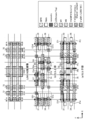
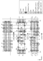
- FIG. 5 is a plan view showing another example of the layout structure of the 2-port SRAM cell according to the first embodiment.
- FIG. 5 is a plan view showing another example of the layout structure of the 2-port SRAM cell according to the first embodiment.
- FIG. 5 is a plan view showing another example of the layout structure of the 2-port SRAM cell according to the first embodiment.
- FIG. 5 is a plan view showing another example of the layout structure of the 2-port SRAM cell according to the first embodiment.
- FIG. 5 is a plan view showing another example of the layout structure of the 2-port SRAM cell according to the first embodiment.
- FIG. 5 is a plan view showing another example of the layout structure of the 2-port SRAM cell according to the first embodiment.
- FIG. 5 is a plan view showing another example of the layout structure of the 2-port SRAM cell according to the first embodiment.
- the plan view which shows the example of the layout structure of the 2-port SRAM cell which concerns on 2nd Embodiment.
- FIG. 5 is a plan view showing another example of the layout structure of the 2-port SRAM cell according to the second embodiment.
- FIG. 5 is a plan view showing another example of the layout structure of the 2-port SRAM cell according to the second embodiment.
- FIG. 5 is a plan view showing another example of the layout structure of the 2-port SRAM cell according to the second embodiment.
- FIG. 5 is a plan view showing another example of the layout structure of the 2-port SRAM cell according to the second embodiment.
- FIG. 5 is a plan view showing another example of the layout structure of the 2-port SRAM cell according to the second embodiment.
- FIG. 5 is a plan view showing another example of the layout structure of the 2-port SRAM cell according to the second embodiment.
- FIG. 5 is a plan view showing another example of the layout structure of the 2-port SRAM cell according to the second embodiment.
- FIG. 5 is a plan view showing another example of the layout structure of the 2-port SRAM cell according to the second embodiment.
- FIG. 5 is a plan view showing another example of the layout structure of the 2-port SRAM cell according to the second embodiment.
- FIG. 5 is a plan view showing another example of the layout structure of the 2-port SRAM cell according to the second embodiment.
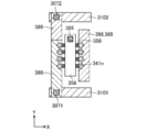
- FIG. 5 is a cross-sectional view showing the structure of a semiconductor device provided with a CFET.
- FIG. 5 is a cross-sectional view showing the structure of a semiconductor device provided with a CFET.
- FIG. 5 is a cross-sectional view showing the structure of a semiconductor device provided with a CFET.
- FIG. 5 is a cross-sectional view showing the structure of a
- the semiconductor storage device comprises a plurality of SRAM cells (in the present specification, as appropriate, simply referred to as cells), and at least a part of the plurality of SRAM cells is a CFET, that is, a three-dimensional structure. It is assumed that a three-dimensional structure device in which P-type FETs and N-type FETs are laminated in a direction perpendicular to a substrate is provided.
- FIGS. 17 to 20 are views showing the structure of a semiconductor device provided with a CFET
- FIG. 17 is a sectional view in the X direction
- FIG. 18 is a sectional view of a gate portion in the Y direction
- FIG. 19 is a source / drain in the Y direction.
- a cross-sectional view of the portion, FIG. 20 is a plan view.
- the X direction is the direction in which the nanowires extend
- the Y direction is the direction in which the gate extends
- the Z direction is the direction perpendicular to the substrate surface.
- FIGS. 17 to 20 are schematic views, and the dimensions and positions of the respective parts are not necessarily consistent.
- an element separation region 302 is formed on the surface of a semiconductor substrate 301 such as a silicon (Si) substrate, and the element active region 30a is defined by the element separation region 302.
- a semiconductor substrate 301 such as a silicon (Si) substrate
- the element active region 30a is defined by the element separation region 302.
- an N-type FET is formed on the P-type FET.
- a laminated transistor structure 390a is formed on the semiconductor substrate 301.
- the laminated transistor structure 390a includes a gate structure 391 formed on the semiconductor substrate 301.
- the gate structure 391 includes a gate electrode 356, a plurality of nanowires 358, a gate insulating film 355, and an insulating film 357.
- the gate electrode 356 extends in the Y direction and rises in the Z direction.
- the nanowires 358 penetrate the gate electrode 356 in the X direction and are arranged in the Y and Z directions.
- the gate insulating film 355 is formed between the gate electrode 356 and the nanowire 358.
- the gate electrode 356 and the gate insulating film 355 are formed at positions recessed from both ends of the nanowire 358 in the X direction, and the insulating film 357 is formed at the recessed portions.
- Insulating films 316 are formed on the semiconductor substrate 301 on both sides of the insulating film 357.
- Reference numerals 321 and 322 are interlayer insulating films.
- the gate electrode 356 is connected to the upper layer wiring by the via 385 provided in the opening 375.
- titanium, titanium nitride, polycrystalline silicon, or the like can be used for the gate electrode 356.
- a high dielectric constant material such as hafnium oxide, aluminum oxide, or oxides of hafnium and aluminum can be used for the gate insulating film 355.
- silicon or the like can be used for the nanowire 358.
- silicon oxide, silicon nitride, or the like can be used for the insulating film 316 and the insulating film 357.
- the number of nanowires 358 arranged in the Z direction is 4, and in the element active region 30a, a P-type semiconductor layer 331p is formed at each end of the two nanowires 358 on the semiconductor substrate 301 side. ..
- Two local wirings 386 in contact with the P-type semiconductor layer 331p are formed so as to sandwich the gate structure 391 in the X direction.
- an N-type semiconductor layer 341n is formed at each end of the two nanowires 358 on the side separated from the semiconductor substrate 101.
- Two local wirings 388 in contact with the N-type semiconductor layer 341n are formed so as to sandwich the gate structure 391 in the X direction.
- An insulating film 332 is formed between the local wiring 386 and the local wiring 388.
- An insulating film 389 is formed on the local wiring 388.
- the P-type semiconductor layer 331p is a P-type SiGe layer
- the N-type semiconductor layer 341n is an n-type Si layer.
- silicon oxide, silicon nitride, or the like can be used for the insulating film 332.
- the local wiring 388 is connected to the embedded wiring 3101 via the via 3071.
- the local wiring 386 is connected to the embedded wiring 3102 via the via 3072.
- the laminated transistor structure 390a has a P-type FET including a gate electrode 356, nanowires 358, a gate insulating film 355, and a P-type semiconductor layer 331p.
- a P-type FET including a gate electrode 356, nanowires 358, a gate insulating film 355, and a P-type semiconductor layer 331p.
- one P-type semiconductor layer 331p functions as a source region
- the other P-type semiconductor layer 331p functions as a drain region
- nanowire 358 functions as a channel.
- the laminated transistor structure 390a also has an N-type FET including a gate electrode 356, nanowires 358, a gate insulating film 355, and an N-type semiconductor layer 341n.
- one N-type semiconductor layer 341n functions as a source region
- the other N-type semiconductor layer 341n functions as a drain region
- nanowire 358 functions as a channel.
- wiring between transistors is performed by vias and metal wiring, but these can be realized by a known wiring process.
- the number of nanowires in the P-type FET and the N-type FET is assumed to be four in the Y direction and two in the Z direction, respectively, for a total of eight, but the number of nanowires is limited to this. It is not something that can be done. Further, the number of nanowires of the P-type FET and the N-type FET may be different.
- the semiconductor layer portion formed at both ends of the nanowire and forming the terminal serving as the source or drain of the transistor is referred to as a "pad".
- the P-type semiconductor layer 331p and the N-type semiconductor layer 341n correspond to pads.
- each insulating film and the like may be omitted.
- the nanowires and the pads on both sides thereof may be described in a simplified linear shape.
- expressions such as "same size” and the like that mean that the sizes and the like are the same include a range of manufacturing variation.
- the source and drain of the transistor are appropriately referred to as "nodes" of the transistor. That is, one node of the transistor refers to the source or drain of the transistor, and both nodes of the transistor refer to the source and drain of the transistor.
- the P-type FET and the N-type FET are basically laminated, but in some cases, the P-type FET or the N-type FET is formed only in the upper layer (or lower layer). ..
- the forming method for example, after forming the upper layer (or lower layer) device, the upper layer (or lower layer) device is partially removed (for example, the removal of the pad portion or the removal of the gate wiring and the pad portion). As a result, a P-type FET or an N-type FET can be formed only in the upper layer (or lower layer).
- the pad portion of the upper layer (or lower layer) device is formed by epitaxial growth, the upper layer (or lower layer) is partially non-formed, so that the P-type FET or the N-type FET is provided only in the upper layer (or lower layer). Can be formed.
- a P-type FET and an N-type FET are basically laminated, but in some cases, the same conductive type FET (P-type FET or N-type FET) is formed in the upper layer and the lower layer. Are laminated. That is, different conductive FETs may be formed in at least one of the upper layer and the lower layer.
- P-type FET or N-type FET conductive type FET
- different conductive FETs may be formed in at least one of the upper layer and the lower layer.
- VDD voltage or the power supply itself.
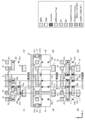
- FIGS. 1 (a), (b) and 2 (c) are plan views
- FIGS. (B) and (c) are cross-sectional views in the horizontal direction in a plan view.
- FIG. 1A shows a portion including a three-dimensional structure transistor formed in the lower part, that is, a side close to the substrate
- FIG. 1B shows a three-dimensional structure formed in the upper part, that is, a side far from the substrate.
- FIG. 1 (c) shows M1 and M2 layers which are metal wiring layers.
- FIG. 2A is a cross section of X1-X1'
- FIG. 2B is a cross section of X2-X2'
- FIG. 2C is a cross section of X3-X3'.
- FIG. 3 is a circuit diagram showing the configuration of the 2-port SRAM cell according to the first embodiment.
- the 2-port SRAM cell according to the present embodiment includes a 2-port SRAM circuit composed of load transistors PU1 and PU2, drive transistors PD1 and PD2, and access transistors PG1 to PG4. ing.
- the load transistors PU1 and PU2 are P-type FETs
- the drive transistors PD1 and PD2 and the access transistors PG1 to PG4 are N-type FETs.
- the load transistor PU1 is provided between the power supply VDD and the first node NA, and the drive transistor PD1 is provided between the first node NA and the power supply VSS.
- the gate of the load transistor PU1 and the drive transistor PD1 is connected to the second node NB, and constitutes the inverter INV1.
- the load transistor PU2 is provided between the power supply VDD and the second node NB, and the drive transistor PD2 is provided between the second node NB and the power supply VSS.
- the gate of the load transistor PU2 and the drive transistor PD2 is connected to the first node NA, and constitutes an inverter INV2. That is, the output of one inverter is connected to the input of the other inverter, thereby forming a latch.
- the access transistor PG1 is provided between the first bit line BLA and the first node NA, and the gate is connected to the first word line WLA.
- the access transistor PG2 is provided between the second bit line BLAX and the second node NB, and the gate is connected to the first word line WLA.
- the access transistor PG3 is provided between the third bit line BLB and the first node NA, and the gate is connected to the second word line WLB.
- the access transistor PG4 is provided between the 4th bit line BLBX and the 2nd node NB, and the gate is connected to the 2nd word line WLB.
- the first and second bit lines BLA and BLAX form a first complementary bit line pair
- the third and fourth bit lines BLB and BLBX form a second complementary bit line pair.
- the first and second bit lines BLA and BLAX constituting the first complementary bit line pair are driven to high level and low level, respectively, and the first word line WLA is driven to high level
- the high level is written to the first node NA and the low level is written to the second node NB.
- the first and second bit lines BLA and BLAX are driven to low level and high level, respectively, and the first word line WLA is driven to high level
- the low level is written to the first node NA and the second node.
- High level is written to NB.
- the latch state is determined and the first and second nodes NA and NB are set. The written data is retained.
- the first and second bit lines BLA and BLAX are precharged to a high level in advance and the first word line WLA is driven to a high level
- the data written to the first and second nodes NA and NB is displayed. Since the states of the first and second bit lines BLA and BLAX are determined accordingly, data can be read from the SRAM cell. Specifically, if the first node NA is at a high level and the second node NB is at a low level, the first bit line BLA holds the high level and the second bit line BLAX is discharged to the low level. On the other hand, if the first node NA is at a low level and the second node NB is at a high level, the first bit line BLA is discharged to the low level and the second bit line BLAX holds the high level.
- the third and fourth bit lines BLB and BLBX constituting the second complementary bit line pair are driven to the high level and the low level, respectively, and the second word line WLB is driven to the high level, the first node NA is reached.
- the high level is written and the low level is written to the second node NB.
- the 3rd and 4th bit lines BLB and BLBX are driven to low level and high level, respectively, and the 2nd word line WLB is driven to high level
- the low level is written to the 1st node NA and the 2nd node.
- the high level is written to NB.
- the latch state is determined and the first and second nodes NA and NB are set. The written data is retained.
- the 3rd and 4th bit lines BLB and BLBX are precharged to a high level in advance and the 2nd word line WLB is driven to a high level
- the data written to the 1st and 2nd nodes NA and NB is displayed. Since the states of the third and fourth bit lines BLB and BLBX are determined accordingly, data can be read from the SRAM cell. Specifically, if the first node NA is at a high level and the second node NB is at a low level, the third bit line BLB holds the high level and the fourth bit line BLBX is discharged to the low level. On the other hand, if the first node NA is low level and the second node NB is high level, the third bit line BLB is discharged to the low level and the fourth bit line BLBX holds the high level.
- the 2-port SRAM cell controls the first and second bit line BLA, BLAX, and the first word line WLA to write data to the SRAM cell, retain data, and the SRAM cell. It has a function to read data from. Further, the 2-port SRAM cell has a function of writing data to the SRAM cell, holding data, and reading data from the SRAM cell by controlling the 3rd and 4th bit lines BLB, BLBX, and the 2nd word line WLB. Has.
- the horizontal direction of the drawing is the X direction
- the vertical direction of the drawing is the Y direction
- the direction perpendicular to the substrate surface is the Z direction.
- the solid line running vertically and horizontally in the plan view of FIG. 1 and the like and the solid line running vertically and horizontally in the cross-sectional view of FIG. 2 and the like indicate a grid used for arranging parts at the time of design.
- the grids are evenly spaced in the X direction and evenly spaced in the Y direction.
- the grid spacing may be the same or different in the X direction and the Y direction. Further, the grid spacing may be different for each layer.
- each component does not necessarily have to be placed on the grid. However, from the viewpoint of suppressing manufacturing variations, it is preferable that the parts are arranged on the grid.
- the dotted line displayed so as to surround the cell in the plan view of FIG. 1 or the like indicates the cell frame of the 2-port SRAM cell (the outer edge of the 2-port SRAM cell).
- the 2-port SRAM cell is arranged so that the cell frame is in contact with the cell frame of the adjacent cell in the X direction or the Y direction.
- power supply wirings 11 and 12 extending in the Y direction are provided at the lower part of the cell, respectively.
- Both the power supply wirings 11 and 12 are embedded power supply wirings (BPR: Buried Power Rail) formed in the embedded wiring layer.
- the power supply wirings 11 and 12 each supply a voltage VSS.
- transistors P1 and P2 correspond to load transistors PU2 and PU1, respectively.
- Transistors N1 and N5 correspond to drive transistor PD1.
- Transistors N2 and N6 correspond to drive transistor PD2.
- Transistors N3, N4, N7, and N8 correspond to access transistors PG1 to PG4, respectively.
- Nanowires 21a to 21c and 26a to 26d extending in the Y direction are formed in the lower part of the cell, and nanowires 21d to 21j extending in the Y direction are formed in the upper part of the cell.
- the nanowires 21a, 26a, 26c are formed side by side in the X direction.
- the nanowires 21b, 21c, 26b, 26d are formed side by side in the X direction.
- the nanowires 21d, 21f, 21g, and 21i are formed side by side in the X direction.
- the nanowires 21e, 21h, 21j are formed side by side in the X direction.
- the nanowires 21d, 21i, 26a and 26c are formed side by side with the nanowires 21e, 21j, 26b and 26d in the Y direction, respectively. Further, the nanowires 21b and 21g are formed at the same position in the X direction in a plan view.
- nanowires 21a, 21c, 26a to 26d overlap with the nanowires 21f, 21h, 21d, 21e, 21i, 21j in a plan view, respectively.
- the gate wirings (Gates) 31 to 36 extend in the Z direction and extend in the X direction from the lower part of the cell to the upper part of the cell.
- the gate wirings 31 to 33 are formed side by side in the X direction, and the gate wirings 34 to 36 are formed side by side in the X direction.
- the gate wiring 31 serves as a gate for the transistor N3 and the dummy transistor N21.
- the gate wiring 32 serves as a gate for the transistors N1, N5, and P2.
- the gate wiring 33 serves as a gate for the transistor N7 and the dummy transistor N23.
- the gate wiring 34 serves as a gate for the transistor N4 and the dummy transistor N22.
- the gate wiring 35 serves as a gate for transistors N2, N6, and P1.
- the gate wiring 36 serves as a gate for the transistor N8 and the dummy transistor N24.
- the nanowires 21a, 21c, 21d to 21f, 21h to 21j form the channel portions of the transistors N1 to N8, respectively.
- the pads 22a and 22b form a node of the transistor N1.
- the pads 22c and 22d form a node of the transistor N2.
- the pads 22e and 22f form a node of the transistor N3.
- the pads 22f and 22g form a node of the transistor N4.
- the pads 22h and 22i form a node of the transistor N5.
- the pads 22j and 22k form a node of the transistor N6.
- the pads 22l and 22m form a node of the transistor N7.
- the pads 22m and 22n form a node of the transistor N8.
- the transistor N1 is composed of the nanowires 21a, the gate wiring 32, and the pads 22a and 22b.
- the transistor N2 is composed of nanowires 21c, gate wiring 35, and pads 22c and 22d.
- the transistor N3 is composed of nanowires 21d, gate wiring 31, and pads 22e and 22f.
- the transistor N4 is composed of nanowires 21e, gate wiring 34, and pads 22f, 22g.
- the transistor N5 is composed of nanowires 21f, gate wiring 32, and pads 22h and 22i.
- the transistor N6 is composed of nanowires 21h, gate wiring 35, and pads 22j and 22k.
- the transistor N7 is composed of nanowires 21i, gate wiring 33, and pads 22l and 22m.
- the transistor N8 is composed of nanowires 21j, gate wiring 36, and pads 22m and 22n.
- Pads 22o to 22r doped with a P-type semiconductor are formed at the upper end of the drawing of the nanowire 21b, the lower end of the drawing of the nanowire 21b, the upper end of the drawing of the nanowire 21g, and the lower end of the drawing of the nanowire 21g, respectively.
- Nanowires 21b and 21g form channel portions of transistors P1 and P2, respectively.
- the pads 22o and 22p form the node of the transistor P1.
- the pads 22q and 22r form a node of the transistor P2.
- the transistor P1 is composed of the nanowire 21b, the gate wiring 35, and the pads 22o and 22p.
- the transistor P2 is composed of 21 g of nanowires, gate wiring 32, and pads 22q and 22r.
- 27f are formed respectively.
- the dummy pads 27a and 27b form a node of the dummy transistor N21.
- the dummy pads 27b and 27c form a node of the dummy transistor N22.
- the dummy pads 27d and 27e form a node of the dummy transistor N23.
- the dummy pads 27e and 27f form a node of the dummy transistor N24.
- the nanowires 26a to 26d correspond to the channel portions of the dummy transistors N21 to N24.
- the dummy transistors N21 to N24 are transistors that do not have a logic function. Further, in the circuit diagram of FIG. 3, the dummy transistors N21 to N24 are omitted. Although some of the 2-port SRAM cells in the embodiments and modifications described below include dummy transistors, each dummy transistor does not affect the logical function of the 2-port SRAM cell. Is omitted.
- the transistors N3 to N8 overlap with the dummy transistors N21 and N22, the transistors N1 and N2, and the dummy transistors N23 and N24, respectively, in a plan view.
- the transistors N1 and the dummy transistors N21 and N23 are formed side by side in the X direction.
- the transistors N2 and P1 and the dummy transistors N22 and N24 are formed side by side in the X direction.
- the transistors N3, N5, N7, and P2 are formed side by side in the X direction.
- the transistors N4, N6, and N8 are formed side by side in the X direction.
- the transistors N3 and N7 and the dummy transistors N21 and N23 are formed side by side with the transistors N4 and N8 and the dummy transistors N22 and N24, respectively, in the Y direction. Further, the transistors P1 and P2 are formed at the same positions in the X direction in a plan view.
- Local wiring (LI: Local Interconnect) 41a to 41e extending in the X direction is formed at the bottom of the cell.
- the local wiring 41a is connected to the pad 22a.
- the local wiring 41b is connected to the pad 22b.
- the local wiring 41c is connected to the pads 22c and 22o.
- the local wiring 41d is connected to the pad 22p.
- the local wiring 41e is connected to the pad 22d.
- Local wiring 41f to 41n extending in the X direction is formed on the upper part of the cell.
- the local wiring 41f is connected to the pad 22e.
- the local wiring 41g is connected to the pad 22h.
- the local wiring 41h is connected to the pad 22q.
- the local wiring 41i is connected to the pad 22l.
- the local wiring 41j is connected to the pads 22f, 22i, 22r.
- the local wiring 41k is connected to the pads 22j and 22m.
- the local wiring 41l is connected to the pad 22g.
- the local wiring 41m is connected to the pad 22k.
- the local wiring 41n is connected to the pad 22n.
- the local wiring 41a is connected to the power supply wiring 11 via the contact (via) 51a, and is connected to the local wiring 41g via the contact 51b.
- the local wiring 41b is connected to the local wiring 41j via the contact 51c.
- the local wiring 41c is connected to the local wiring 41k via the contact 51d.
- the local wiring 41e is connected to the power supply wiring 12 via the contact 51e, and is connected to the local wiring 41m via the contact 51f.
- the local wiring 41j is connected to the gate wiring 35 via the shared-contact 61a.
- the local wiring 41k is connected to the gate wiring 32 via the shared contact 61b.
- the pads of the transistors N1 and N5 are connected to each other by local wiring and contacts, and share the gate wiring.
- the pads of the transistors N2 and N6 are connected to each other by local wiring and contacts, and share the gate wiring.
- the transistors N1 and N5 correspond to the drive transistor PD1
- the transistors N2 and N6 correspond to the drive transistor PD2. Therefore, in the 2-port SRAM cell according to the present embodiment, the drive transistors PD1 and PD2 are each composed of two N-type FETs connected in parallel.
- the local wiring 41b, 41j, contact 51c, shared contact 61a, and gate wiring 35 correspond to the first node NA
- the local wiring 41c, 41k, contact 51d, shared contact 61b, and gate wiring 32 correspond to the second node NB. To do.
- wirings 71 to 75 extending in the Y direction are formed in the M1 wiring layer, which is a metal wiring layer, from both the upper and lower ends of the cell. Further, wirings 76 to 79 are formed.
- the wiring 71 supplies the voltage VDD.
- Wiring 72 to 75 correspond to the first bit line BLA, the third bit line BLB, the second bit line BLAX, and the fourth bit line BLBX, respectively.
- Wiring 81, 82 extending in the X direction is formed on the M2 wiring layer, which is the upper layer of the M1 wiring layer, from both the left and right ends of the cell.
- the wirings 81 and 82 are arranged side by side in the Y direction.
- the wirings 81 and 82 correspond to the first word line WLA and the second word line WLB, respectively.
- the wiring 71 is connected to the local wiring 41h via the contact 91a, and is connected to the local wiring 41d via the contact 91b.
- the wiring 72 is connected to the local wiring 41f via the contact 91c.
- the wiring 73 is connected to the local wiring 41l via the contact 91d.
- the wiring 74 is connected to the local wiring 41i via the contact 91e.
- the wiring 75 is connected to the local wiring 41n via the contact 91f.
- the wiring 76 is connected to the gate wiring 31 via the contact (Gate-contact) 61c, and is connected to the wiring 81 via the contact 91g.
- the wiring 77 is connected to the gate wiring 33 via the contact 61d, and is connected to the wiring 81 via the contact 91h.
- the wiring 78 is connected to the gate wiring 34 via the contact 61e, and is connected to the wiring 82 via the contact 91i.
- the wiring 79 is connected to the gate wiring 36 via the contact 61f, and is connected to the wiring 82 via the contact 91j.
- the wiring 81 is connected to the gate wiring 31 via the contact 91g, the wiring 76, and the contact 61c, and is connected to the gate wiring 33 via the contact 91h, the wiring 77, and the contact 61d.
- the wiring 82 is connected to the gate wiring 34 via the contact 91i, the wiring 78, and the contact 61e, and is connected to the gate wiring 36 via the contact 91j, the wiring 79, and the contact 61f.
- the pad 22q is connected to the wiring 71 that supplies the voltage VDD
- the pad 22r is connected to the local wiring 41j (first node NA)
- the gate wiring 32 is the shared contact 61b (second). It is connected to each node NB).
- the pad 22p is connected to the wiring 71 that supplies the voltage VDD
- the pad 22o is connected to the local wiring 41c (second node NB)
- the gate wiring 35 is connected to the shared contact 61a (first node NA). It is connected.
- the pads 22b and 22i are in local wiring 41b and 41j (first node NA), the pads 22a and 22h are in power supply wiring 11 for supplying voltage VSS, and the gate wiring 32 is in shared contact. They are connected to 61b (second node NB), respectively.
- the pads 22c and 22j make local wiring 41c and 41k (second node NB), the pads 22d and 22k supply voltage VSS to the power supply wiring 12, and the gate wiring 35 makes shared contact. It is connected to each of 61a (first node NA).
- the pad 22e is connected to the wiring 72 (first bit line BLA)
- the pad 22f is connected to the local wiring 41j (first node NA)
- the gate wiring 31 is connected to the wiring 81 (first word line WLA).
- the pad 22l is connected to the wiring 74 (second bit line BLAX)
- the pad 22m is connected to the local wiring 41k (second node NB)
- the gate wiring 33 is connected to the wiring 81 (first word line WLA).
- the pad 22g is connected to the wiring 73 (third bit line BLB), the pad 22f is connected to the local wiring 41j (first node NA), and the gate wiring 34 is connected to the wiring 82 (second word line WLB).
- the pad 22n is connected to the wiring 75 (4th bit line BLBX)
- the pad 22m is connected to the local wiring 41k (second node NB)
- the gate wiring 36 is connected to the wiring 82 (second word line WLB).
- a 2-port SRAM circuit is composed of transistors N1 to N8, P1 and P2.
- transistors N1, N2 and P1 are formed in the lower part of the cell, and transistors N3 to N8 and P2 are formed in the upper part of the cell.
- the transistors N1 to N8, P1 and P2 are three-dimensional structure transistors, respectively. As a result, a 2-port SRAM cell using a CFET can be realized.
- the transistors P1 and P2 are formed at the same position in the X direction in a plan view. As a result, the area of the 2-port SRAM cell can be reduced.
- the drive transistor PD1 is composed of transistors N1 and N5 connected in parallel
- the drive transistor PD2 is composed of transistors N2 and N6 connected in parallel.
- the transistors N1 and N2 overlap with the transistors N5 and N6 in a plan view, respectively. As a result, the area can be reduced while improving the driving capacity of the 2-port SRAM cell.
- the 2-port SRAM cells When the 2-port SRAM cells are arranged adjacent to each other in the X direction, they may be arranged by inverting them in the X direction or they may be arranged without inverting them in the X direction. Further, when the 2-port SRAM cells are arranged adjacent to each other in the Y direction, they are arranged so as to be inverted in the Y direction.
- the dummy transistors N21 to N24 do not affect the logic function of the 2-port SRAM cell. Further, although the dummy transistors N21 to N24 may not be formed, it is possible to suppress the manufacturing variation of the semiconductor storage device, improve the yield, and improve the reliability by forming the dummy transistors N21 to N24. ..
- the shared contact 61a connecting the local wiring 41j and the gate wiring 35 and the shared contact 61b connecting the local wiring 41k and the gate wiring 32 connect the wiring arranged in the M1 wiring layer and the gate wiring.
- the contacts 61c to 61f may be formed in the same process step, or may be formed in another process step.
- the wiring 71 for supplying the voltage VDD is provided in the M1 wiring layer
- the wiring for supplying the voltage VDD may be provided in the embedded wiring layer.
- wiring for supplying the voltage VDD may be provided in both the M1 wiring layer and the embedded wiring layer. In this case, since the power supply for supplying the voltage VDD is strengthened, the power supply can be stabilized.
- the transistors N3, N4, N7 and N8 are formed in the upper part of the cell, the transistors N3, N4, N7 and N8 may be formed in the lower part of the cell. In this case, the transistors N3, N4, N7, and N8 are formed in the lower part of the cell instead of the dummy transistors N21 to N24. Then, local wiring and contacts are formed in the 2-port SRAM cell so that the above-mentioned 2-port SRAM circuit is formed.
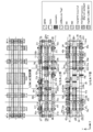
- FIG. 4 is a plan view showing another example of the layout structure of the 2-port SRAM cell according to the first embodiment. Specifically, FIG. 4A shows the lower part of the cell, FIG. 4B shows the upper part of the cell, and FIG. 4C shows the M1 and M2 wiring layers.
- transistors N11 to N14, N17, and N18 are formed in the lower part of the cell in addition to transistors N1, N2, and P1, and dummy transistors N21 to N24 are omitted. Further, in addition to the transistors N3 to N8 and P2, the transistors N15 and N16 are formed on the upper part of the cell.
- nanowires 23a, 23c, 23d, 23e, 23i, 23j extending in the Y direction are formed in the lower part of the cell, and nanowires 23f, 23h extending in the Y direction are formed in the upper part of the cell.
- the nanowires 23a, 23d, 23i are formed side by side with the nanowires 21a in the X direction.
- the nanowires 23c, 23e, 23j are formed side by side with the nanowires 21b, 21c in the X direction.
- the nanowires 23f are formed side by side with the nanowires 21d, 21f, 21g, 21i in the X direction.
- the nanowires 23h are formed side by side with the nanowires 21e, 21h, 21j in the X direction.
- nanowires 23d and 23i are formed side by side with the nanowires 23e and 23j in the Y direction, respectively.
- nanowires 23a, 23c, 23d, 23e, 23i, 23j overlap with the nanowires 23f, 23h, 21d, 21e, 21i, 21j in a plan view, respectively.
- the gate wiring 31 serves as the gate of the transistor N13.
- the gate wiring 32 serves as a gate for the transistors N11 and N15.
- the gate wiring 33 serves as a gate for the transistor N17.
- the gate wiring 34 serves as a gate for the transistor N14.
- the gate wiring 35 serves as a gate for the transistors N12 and N16.
- the gate wiring 36 serves as a gate for the transistor N18.
- Nanowires 23a, 23c, 23d, 23e, 23f, 23h, 23i, 23j form a channel portion of transistors N11 to N18.
- the pads 24a and 24b form a node of the transistor N11.
- the pads 24c and 24d form a node of the transistor N12.
- the pads 24e and 24f form a node of the transistor N13.
- the pads 24f and 24g form a node of the transistor N14.
- the pads 24h and 24i form a node of the transistor N15.
- the pads 24j and 24k form a node of the transistor N16.
- the pads 24l and 24m form a node of the transistor N17.
- the pads 24m and 24n form a node of the transistor N18.
- the transistor N11 is composed of the nanowires 23a, the gate wiring 32, and the pads 24a and 24b.
- the transistor N12 is composed of nanowires 23c, gate wiring 35, and pads 24c, 24d.
- the transistor N13 is composed of nanowires 23d, gate wiring 31, and pads 24e and 24f.
- the transistor N14 is composed of nanowires 23e, gate wiring 34, and pads 24f, 24g.
- the transistor N15 is composed of nanowires 23f, gate wiring 32, and pads 24h and 24i.
- the transistor N16 is composed of nanowires 23h, gate wiring 35, and pads 24j and 24k.
- the transistor N17 is composed of nanowires 23i, gate wiring 33, and pads 24l, 24m.
- the transistor N18 is composed of nanowires 23j, gate wiring 36, and pads 24m and 24n.
- the transistors N11 to N14, N17, and N18 overlap with the transistors N15, N16, N3, N4, N7, and N8 in a plan view, respectively.
- the transistors N11, N13, and N17 are formed side by side with the transistors N1 in the X direction.
- the transistors N12, N14, and N18 are formed side by side with the transistors N2 and P1 in the X direction.
- the transistor N15 is formed side by side with the transistors N3, N5, N7, and P2 in the X direction.
- the transistor N16 is formed side by side with the transistors N4, N6, and N8 in the X direction.
- the transistors N13 and N17 are formed side by side with the transistors N14 and N18 in the Y direction, respectively.
- Local wirings 42a to 42d extending in the X direction are formed at the bottom of the cell.
- the local wiring 42a is connected to the pad 24e.
- the local wiring 42b is connected to the pad 24l.
- the local wiring 42c is connected to the pad 24g.
- the local wiring 42d is connected to the pad 24n.
- the local wiring 41a is connected to the pads 22a and 24a.
- the local wiring 41b is connected to the pads 22b, 24b, 24f.
- the local wiring 41c is connected to the pads 22c, 22o, 24c, 24m.
- the local wiring 41e is connected to the pads 22d and 24d.
- the local wiring 41g is connected to the pads 22h and 24h.
- the local wiring 41j is connected to the pads 22f, 22i, 24i.
- the local wiring 41k is connected to the pads 22j, 22m, 22r, 24j.
- the local wiring 41m is connected to the pads 22k and 24k.
- the local wiring 42a is connected to the local wiring 41f via the contact 52a.
- the local wiring 42b is connected to the local wiring 41i via the contact 52b.
- the local wiring 42c is connected to the local wiring 41l via the contact 52c.
- the local wiring 42d is connected to the local wiring 41n via the contact 52d.
- the pads of each other are connected by local wiring and contacts, and share the gate wiring.
- the pads of each other are connected by local wiring and contacts, and share the gate wiring.
- the pads of the transistors N3 and N13 are connected to each other by local wiring and contacts, and share the gate wiring.
- the pads of the transistors N4 and N14 are connected to each other by local wiring and contacts, and share the gate wiring.
- the pads of the transistors N7 and N17 are connected to each other by local wiring and contacts, and share the gate wiring.
- the pads of the transistors N8 and N18 are connected to each other by local wiring and contacts, and share the gate wiring.
- the transistors N1, N5, N11, and N15 correspond to the drive transistor PD1
- the transistors N2, N6, N12, and N16 correspond to the drive transistor PD2
- the transistors N3 and N13 correspond to the access transistor PG1.
- Transistors N7 and N17 correspond to access transistor PG2
- transistors N4 and N14 correspond to access transistor PG3
- transistors N8 and N18 correspond to access transistor PG4.
- the drive transistors PD1 and PD2 are each composed of four N-type FETs connected in parallel, and the access transistors PG1 to PG4 are each composed of two N-type FETs connected in parallel. ing. Further, the transistors corresponding to the drive transistors PD1 and PD2 and the transistors corresponding to the access transistors PG1 to PG4 are laminated. Then, according to this modification, the same effect as that of the 2-port SRAM cell according to the first embodiment can be obtained.
- the drive transistor PD1 is composed of transistors N1, N5, N11 and N15 connected in parallel
- the drive transistor PD2 is composed of transistors N2, N6, N12 and N16 connected in parallel
- the access transistor PG1 is in parallel.
- the access transistor PG2 is composed of the connected transistors N3 and N13
- the access transistor PG2 is composed of the transistors N7 and N17 connected in parallel
- the access transistor PG3 is composed of the transistors N4 and N14 connected in parallel
- the access transistor PG4 is composed of the transistors N4 and N14 connected in parallel. It is composed of transistors N8 and N18 connected in parallel.
- the transistors N11 to N14, N17, and N18 overlap with the transistors N15, N16, N3, N4, N7, and N8 in a plan view, respectively. As a result, the area can be reduced while improving the driving capacity of the 2-port SRAM cell.
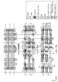
- FIG. 5 is a plan view showing another example of the layout structure of the 2-port SRAM cell according to the first embodiment. Specifically, FIG. 5A shows the lower part of the cell, FIG. 5B shows the upper part of the cell, and FIG. 5C shows the M1 and M2 wiring layers. In FIG. 5, in comparison with FIG. 1, the transistor P1 is formed in the upper part of the cell. Further, dummy transistors N25 and N26 are formed in the lower part of the cell.
- nanowires 21b are formed on the upper part of the cell.
- Nanowires 28a and 28b extending in the Y direction are formed in the lower part of the cell.
- the nanowires 21b are formed side by side with the nanowires 21e, 21h, 21j in the X direction.
- the nanowires 28a are formed side by side with the nanowires 21a, 26a, 26c in the X direction.
- the nanowires 28b are formed side by side with the nanowires 21c, 26b, 26d in the X direction.
- nanowires 21g and 21b overlap with the nanowires 28a and 28b in a plan view, respectively.
- N-type semiconductor-doped dummy pads 29a to 29d are formed at the upper end of the drawing of the nanowire 28a, the lower end of the drawing of the nanowire 28a, the upper end of the drawing of the nanowire 28b, and the lower end of the drawing of the nanowire 28b.
- the nanowires 28a and 28b form channel portions of the dummy transistors N25 and N26, respectively.
- the dummy pads 29a and 29b form a node of the dummy transistor N25, and the dummy pads 29c and 29d form a node of the dummy transistor N26.
- the dummy transistors N25 and N26 are transistors having no logic function.
- the transistors P2 and P1 overlap with the dummy transistors N25 and N26 in a plan view, respectively.
- the transistor P1 is formed side by side with the transistors N4, N6, N8 in the X direction.
- the dummy transistor N25 is formed side by side with the transistor N1 and the dummy transistors N21 and N23 in the X direction.
- the dummy transistor N26 is formed side by side with the transistor N2 and the dummy transistors N22 and N24 in the X direction.
- the local wiring 41c is connected to the pad 22c.
- the local wiring 41k is connected to the pads 22o, 22j, 22m.
- each transistor including the dummy transistor is stacked. Further, the transistor including the dummy transistor formed in the lower part of the cell is only an N-type FET. Then, according to this modification, the same effect as that of the 2-port SRAM cell according to the first embodiment can be obtained.
- the transistors N3 to N8, P2 and P1 overlap with the dummy transistors N21 and N22, the transistors N1 and N2 and the dummy transistors N23 to N26 in a plan view, respectively. That is, each transistor including the dummy transistor is laminated with other transistors. As a result, it is not necessary to remove some of the transistors, so that the complexity of the manufacturing process can be suppressed.
- transistors N1 and N2 and dummy transistors N21 to N26 are formed in the lower part of the cell, and transistors P1, P2 and N3 to N8 are formed in the upper part of the cell. That is, only the N-type FET is arranged in the lower part of the cell, and the above configuration can be realized by replacing a part of the transistors arranged in the upper part of the cell with the N-type FET. As a result, the complexity of the manufacturing process can be suppressed.
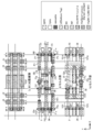
- FIG. 6 is a plan view showing another example of the layout structure of the 2-port SRAM cell according to the first embodiment. Specifically, FIG. 6A shows the lower part of the cell, FIG. 6B shows the upper part of the cell, and FIG. 6C shows the M1 and M2 wiring layers.
- FIG. 6 in comparison with FIG. 1, in addition to the transistors N1 and N2, the transistors N11 to N14, N17, N18 and the dummy transistors N25 and N26 are formed in the lower part of the cell, and the dummy transistors N21 to N24 are omitted. ing. Further, in addition to the transistors N3 to N8 and P2, the transistors N15, N16 and P1 are formed on the upper part of the cell.
- Local wirings 42a to 42d are formed at the bottom of the cell. At the top of the cell, the local wiring 41j is connected to the pads 22f, 22i, 22r, 24i. The local wiring 41k is connected to the pads 22j, 22m, 22o, 24j.
- the transistors N1, N5, N11, and N15 correspond to the drive transistor PD1
- the transistors N2, N6, N12, and N16 correspond to the drive transistor PD2
- the transistors N3 and N13 correspond to the access transistor PG1.
- Transistors N7 and N17 correspond to access transistor PG2
- transistors N4 and N14 correspond to access transistor PG3
- transistors N8 and N18 correspond to access transistor PG4.
- the drive transistors PD1 and PD2 are each composed of four N-type FETs connected in parallel, and the access transistors PG1 to PG4 are each composed of two N-type FETs connected in parallel. It is configured. Further, each transistor including a dummy transistor is laminated. Further, the transistor including the dummy transistor formed in the lower part of the cell is only an N-type FET. Then, according to this modification, the same effect as that of the 2-port SRAM cell according to the first embodiment can be obtained.
- the drive transistor PD1 is composed of transistors N1, N5, N11 and N15 connected in parallel
- the drive transistor PD2 is composed of transistors N2, N6, N12 and N16 connected in parallel
- the access transistor PG1 is in parallel.
- the access transistor PG2 is composed of the connected transistors N3 and N13
- the access transistor PG2 is composed of the transistors N7 and N17 connected in parallel
- the access transistor PG3 is composed of the transistors N4 and N14 connected in parallel
- the access transistor PG4 is composed of the transistors N4 and N14 connected in parallel. It is composed of transistors N8 and N18 connected in parallel.
- the transistors N11 to N14, N17, and N18 overlap with the transistors N15, N16, N3, N4, N7, and N8 in a plan view, respectively. As a result, the area can be reduced while improving the driving capacity of the 2-port SRAM cell.
- the transistors N3 to N8, N15, N16, P1 and P2 overlap with the transistors N13, N14, N1, N2, N17, N18, N11, N12 and the dummy transistors N26 and N25, respectively, in a plan view. That is, each transistor including the dummy transistor is laminated with other transistors. As a result, it is not necessary to remove some of the transistors, so that the complexity of the manufacturing process can be suppressed.
- transistors N1, N2, N11 to N14, N17, N18 and dummy transistors N25 and N26 are formed in the lower part of the cell
- transistors N3 to N8, N15, N16, P1 and P2 are formed in the upper part of the cell.
- FIG. 7 is a plan view showing another example of the layout structure of the 2-port SRAM cell according to the first embodiment. Specifically, FIG. 7A shows the lower part of the cell, FIG. 7B shows the upper part of the cell, and FIG. 7C shows the M1 and M2 wiring layers.
- transistors N5 and N6 are formed in the lower part of the cell in addition to the transistors N1 and N2 and the dummy transistors N21 to N24. Further, in addition to the transistors N3, N4, N7, N8, and P2, the transistors P1 and the dummy transistors P21 and P22 are formed on the upper part of the cell.
- nanowires 21f and 21h are formed at the bottom of the cell.
- Nanowires 21b and nanowires 28c and 28d extending in the Y direction are formed on the upper part of the cell.
- the nanowires 21f are formed side by side with the nanowires 21a, 26a, 26c in the X direction.
- the nanowires 21h are formed side by side with the nanowires 21c, 26b, 26d in the X direction.
- the nanowires 28c are formed side by side with the nanowires 21d, 21g, 21i in the X direction.
- the nanowires 21b and 28d are formed side by side with the nanowires 21e and 21j in the X direction.
- nanowires 21a, 21f, 21c and 21h overlap with the nanowires 21g, 28c, 28d and 21b in a plan view, respectively.
- Dummy pads 29e to 29h doped with a P-type semiconductor are formed at the upper end of the drawing of the nanowire 28c, the lower end of the drawing of the nanowire 28c, the upper end of the drawing of the nanowire 28d, and the lower end of the drawing of the nanowire 28d, respectively.
- the nanowires 28c and 28d form the channel portions of the dummy transistors P21 and P22, respectively.
- the dummy pads 29e and 29f form a node of the dummy transistor P21, and the dummy pads 29g and 29h form a node of the dummy transistor P22.
- the dummy transistors P21 and P22 are transistors having no logic function.
- the transistors P1 and P2 and the dummy transistors P21 and P22 overlap with the transistors N6, N1, N5 and N2 in a plan view, respectively.
- the transistors N5 and N6 are formed side by side with the transistors N1 and N2 in the X direction, respectively.
- wirings 71a and 71b extending in the X direction are formed in the M1 wiring layer.
- the wirings 71a and 71b each supply a voltage VDD.
- the wiring 71a is connected to the local wiring 41h via the contact 91a.
- the wiring 71b is connected to the local wiring 41d via the contact 91b.
- transistors corresponding to drive transistors PD1 and PD2 are formed side by side in the X direction at the bottom of the cell. Further, a transistor corresponding to the load transistors PU1 and PU2 is formed on the upper part of the cell, and is laminated with a transistor corresponding to the drive transistors PD1 and PD2. Then, according to this modification, the same effect as that of the 2-port SRAM cell according to the first embodiment can be obtained.
- the transistors N1, N2, N5, N6 and the dummy transistors N21 to N24 overlap the transistors P2, the dummy transistors P22, P21 and the transistors P1, N3, N4, N7, N8 in a plan view, respectively. That is, each transistor including the dummy transistor is laminated with other transistors. As a result, it is not necessary to remove some of the transistors, so that the complexity of the manufacturing process can be suppressed.
- transistors N1, N2, N5, N6 and dummy transistors N21 to N24 are formed in the lower part of the cell
- transistors N3, N4, N7, N8, P1, P2 and dummy transistors P21, P22 are formed in the upper part of the cell. Is formed. That is, only the N-type FET is arranged in the lower part of the cell, and the above configuration can be realized by replacing a part of the transistors arranged in the upper part of the cell with the N-type FET. As a result, the complexity of the manufacturing process can be suppressed.
- FIG. 8 is a diagram showing an example of the layout structure of the 2-port SRAM cell according to the second embodiment. Specifically, FIG. 8A shows the lower part of the cell, FIG. 8B shows the upper part of the cell, and FIG. 8C shows the M1 and M2 wiring layers.
- transistors N1, N2, N7, N8, N47, N48, and P1 are formed in the lower part of the cell, and transistors N3 to N6, N43, N44, and P2 are formed in the upper part of the cell.
- another 2-port SRAM cell is arranged adjacent to the 2-port SRAM cell according to the present embodiment in the X direction.
- the transistors N43 and N44 are transistors included in the 2-port SRAM cell arranged on the right side of the drawing of the 2-port SRAM cell according to the present embodiment. Further, the transistors N47 and N48 are transistors included in the 2-port SRAM cell arranged on the left side of the drawing of the 2-port SRAM cell according to the present embodiment.
- nanowires 21i and 21j are formed at the bottom of the cell. Further, nanowires 121i and 121j extending in the Y direction are formed at the left end of the drawing at the lower part of the cell, and nanowires 121d and 121e extending in the Y direction are formed at the right end of the drawing at the upper part of the cell.
- the nanowires 121d are formed side by side with the nanowires 21d, 21f, 21g in the X direction.
- the nanowires 121e are formed side by side with the nanowires 21e and 21h in the X direction.
- the nanowires 121i are formed side by side with the nanowires 21a and 21i in the X direction.
- the nanowires 121j are formed side by side with the nanowires 21b, 21c, 21j in the X direction.
- nanowires 121d and 121e are formed side by side in the Y direction.
- the nanowires 121i and 121j are formed side by side in the Y direction.
- nanowires 121d, 121e, 121i, 121j overlap with the nanowires 21i, 21j, 21d, 21e in a plan view, respectively.
- the gate wiring 33 serves as the gate of the transistor N43.
- the gate wiring 36 serves as a gate for the transistor N44.
- the gate wiring 31 serves as a gate for the transistor N47.
- the gate wiring 34 serves as a gate for the transistor N48.
- the transistors N43 and N44 overlap with the transistors N7 and N8 in a plan view, respectively.
- the transistors N47 and N48 overlap with the transistors N3 and N4 in a plan view, respectively.
- the transistor N43 is formed side by side with the transistors N3, N5, P2 in the X direction.
- the transistor N44 is formed side by side with the transistors N4 and N6 in the X direction.
- the transistor N47 is formed side by side with the transistors N1 and N7 in the X direction.
- the transistor N48 is formed side by side with the transistors N2, N8, and P1 in the X direction.
- the transistors N43 and N44 are formed side by side in the Y direction.
- the transistors N47 and N48 are formed side by side in the Y direction.
- the local wiring 41c is connected to the pads 22c, 22m, 22o.
- the local wiring 41k is connected to the pad 22j.
- a 2-port SRAM circuit is configured by the transistors N1 to N8, P1 and P2. Further, transistors N1, N2, N7, N8, and P1 are formed in the lower part of the cell, and transistors N3 to N6 and P2 are formed in the upper part of the cell.
- the transistors N1 to N8, P1 and P2 are three-dimensional structure transistors, respectively. As a result, a 2-port SRAM cell using a CFET can be realized.
- the transistors P1 and P2 are formed at the same position in the X direction in a plan view. As a result, the area of the 2-port SRAM cell can be reduced.
- the drive transistor PD1 is composed of transistors N1 and N5 connected in parallel
- the drive transistor PD2 is composed of transistors N2 and N6 connected in parallel.
- the transistors N1 and N2 overlap with the transistors N5 and N6 in a plan view, respectively. As a result, the area can be reduced while improving the driving capacity of the 2-port SRAM cell.
- the transistors N43 and N44 correspond to the transistors N3 and N4 in the 2-port SRAM cell arranged on the right side of the drawing of the 2-port SRAM cell according to the present embodiment, respectively.
- the transistors N47 and N48 correspond to the transistors N7 and N8 in the 2-port SRAM cell arranged on the left side of the drawing of the 2-port SRAM cell according to the present embodiment, respectively.
- the transistors N43 and N44 overlap with the transistors N7 and N8 in a plan view
- the transistors N47 and N48 overlap with the transistors N3 and N4 in a plan view, respectively.
- the transistor N3 corresponding to the access transistor PG1 is laminated with the transistor N47 corresponding to the access transistor PG2 of the 2-port SRAM cell adjacent to the left side of the drawing.
- the transistor N7 corresponding to the access transistor PG2 is laminated with the transistor N43 corresponding to the access transistor PG1 of the 2-port SRAM cell adjacent to the right side of the drawing.
- the transistor N4 corresponding to the access transistor PG3 is laminated with the transistor N48 corresponding to the access transistor PG4 of the 2-port SRAM cell adjacent to the left side of the drawing.
- the transistor N8 corresponding to the access transistor PG4 is laminated with the transistor N44 corresponding to the access transistor PG3 of the 2-port SRAM cell adjacent to the right side of the drawing.
- the 2-port SRAM cells adjacent to each other in the X direction are arranged without being inverted in the X direction. Further, the 2-port SRAM cell and the 2-port SRAM cell adjacent to each other in the Y direction are arranged so as to be inverted in the Y direction.
- the transistors N3, N4, N43, N44 may be formed in the lower part of the cell, and the transistors N7, N8, N47, N48 may be formed in the upper part of the cell.
- local wiring and contacts are formed in the 2-port SRAM cell according to the present embodiment so that the 2-port SRAM cell circuit is formed.
- FIG. 9 is a diagram showing another example of the layout structure of the 2-port SRAM cell according to the second embodiment. Specifically, FIG. 9A shows the lower part of the cell, FIG. 9B shows the upper part of the cell, and FIG. 9C shows the M1 and M2 wiring layers. In FIG. 9, the transistor P1 is formed in the upper part of the cell in comparison with FIG. Further, dummy transistors N25 and N26 are formed in the lower part of the cell.
- nanowires 21b are formed on the upper part of the cell.
- Nanowires 28a and 28b are formed in the lower part of the cell.
- the nanowires 21b are formed side by side with the nanowires 21e, 21h, 121e in the X direction.
- the nanowires 28a are formed side by side with the nanowires 21a, 21i, 121i in the X direction.
- the nanowires 28b are formed side by side with the nanowires 21c, 21j, 121j in the X direction.
- nanowires 21g and 21b overlap with the nanowires 28a and 28b in a plan view, respectively.
- the transistors P2 and P1 overlap with the dummy transistors N25 and N26 in a plan view, respectively.
- the transistor P1 is formed side by side with the transistors N4, N6, N44 in the X direction.
- the dummy transistor N25 is formed side by side with the transistors N1, N7, N47 in the X direction.
- the dummy transistor N26 is formed side by side with the transistors N2, N8, and N48 in the X direction.
- the local wiring 41c is connected to the pads 22c and 22m.
- the local wiring 41k is connected to the pads 22j and 22o.
- each transistor including the dummy transistor is stacked. Further, the transistor including the dummy transistor formed in the lower part of the cell is only an N-type FET. Then, in this modification, the same effect as that of the SRAM cell according to the second embodiment can be obtained.
- the transistors N1, N2, N7, N8, N47, N48 and the dummy transistors N25 and N26 overlap with the transistors N5, N6, N43, N44, N3, N4, P2 and P1 in a plan view, respectively. That is, each transistor including the dummy transistor is laminated with other transistors. As a result, it is not necessary to remove some of the transistors, so that the complexity of the manufacturing process can be suppressed.
- transistors N1, N2, N7, N8, N47, N48 and dummy transistors N25, N26 are formed in the lower part of the cell, and transistors N3 to N6, N43, N44, P1 and P2 are formed in the upper part of the cell.
- the N-type FET is arranged in the lower part of the cell, and the above configuration can be realized by replacing a part of the transistors arranged in the upper part of the cell with the N-type FET. As a result, the complexity of the manufacturing process can be suppressed.
- FIG. 10 is a diagram showing another example of the layout structure of the 2-port SRAM cell according to the second embodiment. Specifically, FIG. 10A shows the lower part of the cell, FIG. 10B shows the upper part of the cell, and FIG. 10C shows the M1 and M2 wiring layers.
- transistors N5 and N6 are formed in the lower part of the cell in addition to the transistors N1, N2, N7, N8, N47, and N48. Further, in addition to the transistors N3, N4, N43, N44, and P2, the transistors P1 and the dummy transistors P21 and P22 are formed on the upper part of the cell.
- nanowires 21f and 21h are formed at the bottom of the cell.
- Nanowires 21b, 28c, 28d are formed on the upper part of the cell.
- the nanowires 21f are formed side by side with the nanowires 21a, 21i, 121i in the X direction.
- the nanowires 21h are formed side by side with the nanowires 21c, 21j, 121j in the X direction.
- the nanowires 28c are formed side by side with the nanowires 21d, 21g, 121d in the X direction.
- the nanowires 21b and 28d are formed side by side with the nanowires 21e and 121e in the X direction.
- nanowires 21a, 21f, 21c and 21h overlap with the nanowires 21g, 28c, 28d and 21b in a plan view, respectively.
- the transistors P1 and P2 and the dummy transistors P21 and P22 overlap with the transistors N6, N1, N5 and N2 in a plan view, respectively.
- the transistor N5 is formed side by side with the transistors N1, N7, N47 in the X direction.
- the transistor N6 is formed side by side with the transistors N2, N6, N8, and N48 in the X direction.
- the local wiring 41a is connected to the pads 22a and 22h.
- the local wiring 41b is connected to the pads 22b and 22i.
- the local wiring 41c is connected to the pads 22c, 22j, 22m.
- the local wiring 41e is connected to the pads 22d and 22k.
- the local wiring 41k is connected to the pad 22o.
- transistors corresponding to drive transistors PD1 and PD2 are formed side by side in the X direction at the bottom of the cell. Further, a transistor corresponding to the load transistors PU1 and PU2 is formed on the upper part of the cell, and is laminated with a transistor corresponding to the drive transistors PD1 and PD2. Then, according to this modification, the same effect as that of the 2-port SRAM cell according to the second embodiment can be obtained.
- the transistors N1, N2, N5 to N8, N47, and N48 overlap the transistors P2, the dummy transistors P22, P21, and the transistors P1, N43, N44, N3, and N4 in a plan view, respectively. That is, each transistor including the dummy transistor is laminated with other transistors. As a result, it is not necessary to remove some of the transistors, so that the complexity of the manufacturing process can be suppressed.
- transistors N1, N2, N5 to N8, N47, N48 are formed in the lower part of the cell
- transistors N3, N4, N43, N44, P1, P2 and dummy transistors P21, P22 are formed in the upper part of the cell.
- the above configuration can be realized by replacing a part of the transistors arranged in the upper part of the cell with the N-type FET. As a result, the complexity of the manufacturing process can be suppressed.
- FIGS. 11 (a) and 12 (a) show the lower part of the cell
- FIGS. 11 (b) and 12 (b) show the upper part of the cell
- FIGS. 11 (c) and 12 (c) show the upper part of the cell.
- the M1 and M2 wiring layers are shown.
- transistors N43 and N44 are formed in the lower part of the cell in addition to the transistors N1, N2, N47, N48 and P1. Further, in addition to the transistors N3 to N6 and P2, the transistors N7 and N8 are formed on the upper part of the cell. In FIG. 12, in comparison with FIG. 8, transistors N3 and N4 are formed in the lower part of the cell in addition to the transistors N1, N2, N7, N8 and P1. Further, in addition to the transistors N5, N6, N43, N44, and P2, the transistors N47 and N48 are formed on the upper part of the cell.
- the 2-port SRAM cells shown in FIGS. 11 and 12 are alternately arranged adjacent to each other in the X direction.
- the transistors N43 and N44 are transistors included in the 2-port SRAM cell shown in FIG. 12 arranged on the right side of the drawing, and the transistors N47 and N48 are shown in FIG. 12 arranged on the left side of the drawing. It is a transistor included in the 2-port SRAM cell shown.
- transistors N43 and N44 are transistors included in the 2-port SRAM cell shown in FIG. 11 arranged on the right side of the drawing, and transistors N47 and N48 are shown in FIG. 11 arranged on the left side of the drawing. It is a transistor included in the port SRAM cell.
- the nanowires 21d, 21e, 21i, 21j overlap with the nanowires 121i, 121j, 121d, 121e, respectively, in a plan view. That is, the transistors N3, N4, N7, and N8 overlap with the transistors N47, N48, N43, and N44 in a plan view, respectively.
- nanowires 121d, 121e, 121i, 121j are formed in the lower part of the cell, and nanowires 21d, 21e, 21i, 21j are formed in the upper part of the cell. Further, nanowires 21a, 121d, 121i are formed side by side in the X direction. Nanowires 21b, 21c, 121e, 121j are formed side by side in the X direction. Nanowires 21d, 21f, 21g, 21i are formed side by side in the X direction. Nanowires 21e, 21h, 21j are formed side by side in the X direction.
- transistors N43, N44, N47, and N48 are formed in the lower part of the cell, and transistors N3, N4, N7, and N8 are formed in the upper part of the cell. Further, the transistors N1, N43, and N47 are formed side by side in the X direction. Transistors N2, N44, N48, and P1 are formed side by side in the X direction. Transistors N3, N5, N7, and P2 are formed side by side in the X direction. Transistors N4, N6, and N8 are formed side by side in the X direction.
- nanowires 21d, 21e, 21i, 21j are formed in the lower part of the cell, and nanowires 121d, 121e, 121i, 121j are formed in the upper part of the cell. Further, nanowires 21a, 21d, 21i are formed side by side in the X direction. Nanowires 21b, 21c, 21e, 21j are formed side by side in the X direction. Nanowires 21f, 21g, 121d, 121i are formed side by side in the X direction. Nanowires 21h, 121e, 121j are formed side by side in the X direction.
- transistors N3, N4, N7, and N8 are formed in the lower part of the cell, and transistors N43, N44, N47, and N48 are formed in the upper part of the cell. Further, the transistors N1, N3, and N7 are formed side by side in the X direction. Transistors N2, N4, N8, and P1 are formed side by side in the X direction. Transistors N5, N43, N47, and P2 are formed side by side in the X direction. Transistors N6, N44, and N48 are formed side by side in the X direction.
- transistors corresponding to access transistors PG1 to PG4 are formed only in either the upper part of the cell or the lower part of the cell. Further, the transistors corresponding to the load transistors are formed at the same positions in the X direction. Further, transistors corresponding to drive transistors PD1 and PD2 are laminated, respectively. Then, according to this modification, the same effect as that of the 2-port SRAM cell according to the second embodiment can be obtained.
- transistors N3, N4, N7, and N8 are formed on the upper part of the cell.
- transistors N3, N4, N7, and N8 are formed in the lower part of the cell. That is, in FIGS. 11 and 12, the transistors corresponding to the access transistors PG1 to PG4 are formed only in either the upper part of the cell or the lower part of the cell. That is, even when the device characteristics of the transistors formed in the upper part of the cell and the lower part of the cell are different, the transistors corresponding to the access transistors PG1 to PG4 are formed in the same layer (either the upper part of the cell or the lower part of the cell).
- the transistors P1 and P2 are formed at the same positions in the X direction in a plan view. As a result, the area of the 2-port SRAM cell can be reduced.
- the drive transistor PD1 is composed of transistors N1 and N5 connected in parallel
- the drive transistor PD2 is composed of transistors N2 and N6 connected in parallel.
- the transistors N1 and N2 overlap with the transistors N5 and N6 in a plan view, respectively. As a result, the area can be reduced while improving the driving capacity of the 2-port SRAM cell.
- the 2-port SRAM cells shown in FIG. 12 are arranged adjacent to the 2-port SRAM cells shown in FIG. 11 without being inverted in the X direction, but the 2-ports shown in FIG. 12 are arranged adjacent to each other.
- the SRAM cells may be inverted in the X direction and arranged adjacent to each other.
- the transistors N43 and N44 correspond to the transistors N7 and N8 in the 2-port SRAM cell shown in FIG. 12 arranged on the right side of the drawing, respectively.
- the transistors N47 and N48 correspond to the transistors N3 and N4 in the 2-port SRAM cell shown in FIG. 12 arranged on the left side of the drawing, respectively.
- FIGS. 13 (a) and 14 (a) show the lower part of the cell
- FIGS. 13 (b) and 14 (b) show the upper part of the cell
- FIGS. 13 (c) and 14 (c) show the upper part of the cell.
- the M1 and M2 wiring layers are shown.
- the transistors N43 and N44 and the dummy transistors N25 and N26 are formed in the lower part of the cell. Further, in addition to the transistors N3 to N6 and P2, the transistors N7, N8 and P1 are formed on the upper part of the cell. In FIG. 14, in comparison with FIG. 8, in addition to the transistors N1, N2, N7, N8, the transistors N3, N4 and the dummy transistors N25, 26 are formed in the lower part of the cell. Further, in addition to the transistors N5, N6, N43, N44, and P2, the transistors N47, N48, and P1 are formed on the upper part of the cell.
- the 2-port SRAM cells shown in FIGS. 13 and 14 are alternately arranged adjacent to each other in the X direction.
- the transistors N43 and N44 are transistors included in the 2-port SRAM cell shown in FIG. 14 arranged on the right side of the drawing, and the transistors N47 and N48 are shown in FIG. 14 arranged on the left side of the drawing. It is a transistor included in the 2-port SRAM cell shown.
- the transistors N43 and N44 are transistors included in the 2-port SRAM cell shown in FIG. 13 arranged on the right side of the drawing, and the transistors N47 and N48 are shown in FIG. 13 arranged on the left side of the drawing. It is a transistor included in the port SRAM cell.
- the nanowires 21d, 21e, 21i, 21j overlap with the nanowires 121i, 121j, 121d, 121e, respectively, in a plan view. That is, the transistors N3, N4, N7, and N8 overlap with the transistors N47, N48, N43, and N44 in a plan view, respectively.
- nanowires 21b are formed in the upper part of the cell, and nanowires 28a and 28b are formed in the lower part of the cell.
- the nanowires 21g and 21b overlap with the nanowires 28a and 28b in a plan view, respectively. That is, the transistors P2 and P1 overlap with the dummy transistors N25 and N26, respectively, in a plan view.
- nanowires 121d, 121e, 121i, 121j are formed in the lower part of the cell, and nanowires 21d, 21e, 21i, 21j are formed in the upper part of the cell. Further, nanowires 21a, 28a, 121d, 121i are formed side by side in the X direction. Nanowires 21c, 28b, 121e, 121j are formed side by side in the X direction. Nanowires 21d, 21f, 21g, 21i are formed side by side in the X direction. Nanowires 21b, 21e, 21h, 21j are formed side by side in the X direction.
- transistors N1, N43, N47 and dummy transistors N25 are formed side by side in the X direction.
- Transistors N2, N44, N48 and dummy transistors N26 are formed side by side in the X direction.
- Transistors N3, N5, N7, and P2 are formed side by side in the X direction.
- Transistors N4, N6, N8, and P1 are formed side by side in the X direction.
- nanowires 21d, 21e, 21i, 21j are formed in the lower part of the cell, and nanowires 121d, 121e, 121i, 121j are formed in the upper part of the cell. Further, nanowires 21a, 21d, 21i, 28a are formed side by side in the X direction. Nanowires 21c, 21e, 21j, 28b are formed side by side in the X direction. Nanowires 21f, 21g, 121d, 121i are formed side by side in the X direction. Nanowires 21b, 21h, 121e, 121j are formed side by side in the X direction.
- the transistors N1, N3, N7 and the dummy transistor N25 are formed side by side in the X direction.
- Transistors N2, N4, N8 and dummy transistors N26 are formed side by side in the X direction.
- Transistors N5, N43, N47, and P2 are formed side by side in the X direction.
- Transistors N6, N44, N48, and P1 are formed side by side in the X direction.
- transistors corresponding to access transistors PG1 to PG4 are formed only in either the upper part of the cell or the lower part of the cell. Further, each transistor including a dummy transistor is laminated. Further, the transistor including the dummy transistor formed in the lower part of the cell is only an N-type FET. Then, according to this modification, the same effect as that of the 2-port SRAM cell according to the second embodiment can be obtained.
- transistors N3, N4, N7, and N8 are formed on the upper part of the cell.
- transistors N3, N4, N7, and N8 are formed in the lower part of the cell. That is, in FIGS. 13 and 14, the transistors corresponding to the access transistors PG1 to PG4 are formed only in either the upper part of the cell or the lower part of the cell. That is, even when the device characteristics of the transistors formed in the upper part of the cell and the lower part of the cell are different, the transistors corresponding to the access transistors PG1 to PG4 are formed in the same layer (either the upper part of the cell or the lower part of the cell).
- the transistors N1, N2, N43, N44, N47, N48 and the dummy transistors N25 and N26 overlap with the transistors N5 to N8, N3, N4, P2 and P1 in a plan view, respectively. That is, in FIGS. 13 and 14, each transistor including the dummy transistor is laminated with other transistors. As a result, it is not necessary to remove some of the transistors, so that the complexity of the manufacturing process can be suppressed.
- transistors N1, N2, N43, N44, N47, N48 and dummy transistors N25, N26 are formed in the lower part of the cell, and transistors N3 to N8, P1 and P2 are formed in the upper part of the cell.
- transistors N1 to N4, N7, N8 and dummy transistors N25 and N26 are formed in the lower part of the cell, and transistors N5, N6, N43, N44, N47, N48, P1 and P2 are formed in the upper part of the cell. Has been done. That is, in FIGS.
- the 2-port SRAM cells shown in FIG. 14 are arranged adjacent to the 2-port SRAM cells shown in FIG. 13 without being inverted in the X direction, but the 2-ports shown in FIG. 14 are arranged adjacent to each other.
- the SRAM cells may be inverted in the X direction and arranged adjacent to each other.
- the transistors N43 and N44 correspond to the transistors N7 and N8 in the 2-port SRAM cell shown in FIG. 14 arranged on the right side of the drawing.
- the transistors N47 and N48 correspond to the transistors N3 and N4 in the 2-port SRAM cell shown in FIG. 14 arranged on the left side of the drawing, respectively.
- FIGS. 15 (a) and 16 (a) show the lower part of the cell
- FIGS. 15 (b) and 16 (b) show the upper part of the cell
- FIGS. 15 (c) and 16 (c) show the upper part of the cell.
- the M1 and M2 wiring layers are shown.
- transistors N5, N6, N43, and N44 are formed in the lower part of the cell in addition to the transistors N1, N2, N47, and N48. Further, in addition to the transistors N3, N4, and P2, the transistors N7, N8, P1 and the dummy transistors P21 and P22 are formed on the upper part of the cell.
- transistors N3 to N6 are formed in the lower part of the cell in addition to the transistors N1, N2, N7, and N8. Further, in addition to the transistors N43, N44 and P2, the transistors N47, N48 and P1 and the dummy transistors P21 and P22 are formed on the upper part of the cell.
- the 2-port SRAM cells shown in FIGS. 15 and 16 are alternately arranged adjacent to each other in the X direction.
- the transistors N43 and N44 are transistors included in the 2-port SRAM cell shown in FIG. 16 arranged on the right side of the drawing, and the transistors N47 and N48 are shown in FIG. 16 arranged on the left side of the drawing. It is a transistor included in the 2-port SRAM cell shown.
- the transistors N43 and N44 are transistors included in the 2-port SRAM cell shown in FIG. 15 arranged on the right side of the drawing, and the transistors N47 and N48 are arranged in FIG. 15 on the left side of the drawing. It is a transistor included in the port SRAM cell.
- the nanowires 21d, 21e, 21i, 21j overlap with the nanowires 121i, 121j, 121d, 121e in a plan view, respectively. That is, the transistors N3, N4, N7, and N8 overlap with the transistors N47, N48, N44, and N47 in a plan view, respectively.
- nanowires 21f and 21h are formed in the lower part of the cell, and nanowires 28c and 28d are formed in the upper part of the cell. Further, the nanowires 21a, 21f, 21c and 21h overlap with the nanowires 21g, 28c, 28d and 21b in a plan view, respectively. That is, the transistors P1 and P2 and the dummy transistors P21 and P22 overlap with the transistors N6, N1, N5 and N2 in a plan view, respectively.
- nanowires 121d, 121e, 121i, 121j are formed in the lower part of the cell, and nanowires 21d, 21e, 21i, 21j are formed in the upper part of the cell. Further, nanowires 21a, 21f, 121d, 121i are formed side by side in the X direction. Nanowires 21c, 21h, 121e, 121j are formed side by side in the X direction. Nanowires 21d, 21g, 21i, 28c are formed side by side in the X direction. Nanowires 21b, 21e, 21j, 28d are formed side by side in the X direction.
- transistors N1, N5, N43, and N47 are formed side by side in the X direction.
- Transistors N2, N6, N44, and N48 are formed side by side in the X direction.
- Transistors N3, N7, P2 and dummy transistors P21 are formed side by side in the X direction.
- Transistors N4, N8, P1 and dummy transistors P22 are formed side by side in the X direction.
- nanowires 21d, 21e, 21i, 21j are formed in the lower part of the cell, and nanowires 121d, 121e, 121i, 121j are formed in the upper part of the cell. Further, nanowires 21a, 21d, 21f, 21i are formed side by side in the X direction. Nanowires 21c, 21e, 21h, 21j are formed side by side in the X direction. Nanowires 21g, 28c, 121d, 121i are formed side by side in the X direction. Nanowires 21b, 28d, 121e, 121j are formed side by side in the X direction.
- transistors N1, N3, N5, and N7 are formed side by side in the X direction.
- Transistors N2, N4, N6, and N8 are formed side by side in the X direction.
- Transistors N43, N47, P2 and dummy transistors P21 are formed side by side in the X direction.
- Transistors N44, N48, P1 and dummy transistors P22 are formed side by side in the X direction.
- transistors corresponding to access transistors PG1 to PG4 are formed only in either the upper part of the cell or the lower part of the cell. Further, transistors corresponding to the drive transistors PD1 and PD2 are formed side by side in the X direction at the lower part of the cell. Further, a transistor corresponding to the load transistors PU1 and PU2 is formed on the upper part of the cell, and is laminated with a transistor corresponding to the drive transistors PD1 and PD2. Then, according to this modification, the same effect as that of the 2-port SRAM cell according to the second embodiment can be obtained.
- transistors N3, N4, N7, and N8 are formed on the upper part of the cell.
- transistors N3, N4, N7, and N8 are formed in the lower part of the cell. That is, in FIGS. 15 and 16, the transistors corresponding to the access transistors PG1 to PG4 are formed only in either the upper part of the cell or the lower part of the cell. That is, even when the device characteristics of the transistors formed in the upper part of the cell and the lower part of the cell are different, the transistors corresponding to the access transistors PG1 to PG4 are formed in the same layer (either the upper part of the cell or the lower part of the cell).
- the transistors N1, N2, N5, N6, N43, N44, N47, and N48 are viewed in plan with the transistors P2, dummy transistors P22, P21, and transistors P1, N7, N8, N3, and N4, respectively. It overlaps with. That is, in FIGS. 15 and 16, each transistor including the dummy transistor is laminated with another transistor. As a result, it is not necessary to remove some of the transistors, so that the complexity of the manufacturing process can be suppressed.
- transistors N1, N2, N5, N6, N43, N44, N47, N48 are formed in the lower part of the cell, and transistors N3, N4, N7, N8, P1, P2 and a dummy are formed in the upper part of the cell.
- Transistors P21 and P22 are formed.
- transistors N1 to N8 are arranged in the lower part of the cell, and transistors N43, N44, N47, N48, P1, P2 and dummy transistors P21 and P22 are formed in the upper part of the cell. That is, in FIGS.
- the 2-port SRAM cells shown in FIG. 16 are arranged adjacent to the 2-port SRAM cells shown in FIG. 15 without being inverted in the X direction, but the 2-ports shown in FIG. 15 are arranged adjacent to each other.
- the SRAM cells may be inverted in the X direction and arranged adjacent to each other.
- the transistors N43 and N44 correspond to the transistors N7 and N8 in the 2-port SRAM cell shown in FIG. 16 arranged on the right side of the drawing.
- the transistors N47 and N48 correspond to the transistors N3 and N4 in the 2-port SRAM cell shown in FIG. 16 arranged on the left side of the drawing.
- each transistor is provided with one nanowire, but a part or all of the transistors may be provided with a plurality of nanowires.
- a plurality of nanowires may be provided in the X direction in a plan view, or a plurality of nanowires may be provided in the Z direction.
- a plurality of nanowires may be provided in both the X direction and the Z direction.
- the number of nanowires included in the transistor may be different between the upper part and the lower part of the cell.
- each transistor may be composed of a plurality of transistors connected in parallel.
- the cross-sectional shape of the nanowire is substantially square, but the present invention is not limited to this. For example, it may be circular or rectangular.
- a nanowire FET has been described as an example as a three-dimensional structure transistor, but the description is not limited to this.
- the transistor formed in the lower part of the cell may be a fin type transistor.
- a 2-port SRAM cell using a CFET can be realized and the area of the 2-port SRAM cell can be reduced. be able to.
Landscapes
- Semiconductor Memories (AREA)
- Static Random-Access Memory (AREA)
Priority Applications (2)
| Application Number | Priority Date | Filing Date | Title |
|---|---|---|---|
| JP2021524796A JP7606101B2 (ja) | 2019-06-03 | 2020-05-27 | 半導体記憶装置 |
| US17/539,695 US12127388B2 (en) | 2019-06-03 | 2021-12-01 | Semiconductor storage device |
Applications Claiming Priority (2)
| Application Number | Priority Date | Filing Date | Title |
|---|---|---|---|
| JP2019-103722 | 2019-06-03 | ||
| JP2019103722 | 2019-06-03 |
Related Child Applications (1)
| Application Number | Title | Priority Date | Filing Date |
|---|---|---|---|
| US17/539,695 Continuation US12127388B2 (en) | 2019-06-03 | 2021-12-01 | Semiconductor storage device |
Publications (1)
| Publication Number | Publication Date |
|---|---|
| WO2020246344A1 true WO2020246344A1 (ja) | 2020-12-10 |
Family
ID=73652476
Family Applications (1)
| Application Number | Title | Priority Date | Filing Date |
|---|---|---|---|
| PCT/JP2020/020975 Ceased WO2020246344A1 (ja) | 2019-06-03 | 2020-05-27 | 半導体記憶装置 |
Country Status (3)
| Country | Link |
|---|---|
| US (1) | US12127388B2 (https=) |
| JP (1) | JP7606101B2 (https=) |
| WO (1) | WO2020246344A1 (https=) |
Cited By (2)
| Publication number | Priority date | Publication date | Assignee | Title |
|---|---|---|---|---|
| WO2025234291A1 (ja) * | 2024-05-08 | 2025-11-13 | 株式会社ソシオネクスト | 半導体記憶装置 |
| WO2025243827A1 (ja) * | 2024-05-21 | 2025-11-27 | 株式会社ソシオネクスト | 半導体記憶装置 |
Families Citing this family (6)
| Publication number | Priority date | Publication date | Assignee | Title |
|---|---|---|---|---|
| JP7590655B2 (ja) * | 2019-06-21 | 2024-11-27 | 株式会社ソシオネクスト | 半導体記憶装置 |
| US11114153B2 (en) * | 2019-12-30 | 2021-09-07 | Taiwan Semiconductor Manufacturing Co., Ltd. | SRAM devices with reduced coupling capacitance |
| US12046652B2 (en) * | 2020-06-25 | 2024-07-23 | Intel Corporation | Plug and recess process for dual metal gate on stacked nanoribbon devices |
| US11488969B1 (en) * | 2021-04-08 | 2022-11-01 | Taiwan Semiconductor Manufacturing Company, Ltd. | Two-port SRAM cells with asymmetric M1 metalization |
| US12349458B2 (en) * | 2022-03-22 | 2025-07-01 | International Business Machines Corporation | Staggered stacked circuits with increased effective width |
| EP4621783A1 (en) * | 2024-03-22 | 2025-09-24 | INTEL Corporation | Balanced static random-access memory (sram) |
Citations (5)
| Publication number | Priority date | Publication date | Assignee | Title |
|---|---|---|---|---|
| JPH0661452A (ja) * | 1992-08-11 | 1994-03-04 | Mitsubishi Electric Corp | 半導体装置 |
| JP2009295975A (ja) * | 2008-06-02 | 2009-12-17 | Commiss Energ Atom | いくつかのレベルのところに集積された、しきい値電圧vtが動的に調整可能なトランジスタを有するsramメモリセル |
| JP2013143536A (ja) * | 2012-01-12 | 2013-07-22 | Toshiba Corp | 半導体装置及びその製造方法 |
| WO2014184933A1 (ja) * | 2013-05-16 | 2014-11-20 | ユニサンティス エレクトロニクス シンガポール プライベート リミテッド | Sgtを有する半導体装置の製造方法 |
| WO2014185085A1 (ja) * | 2013-05-14 | 2014-11-20 | 株式会社 東芝 | 半導体記憶装置 |
Family Cites Families (16)
| Publication number | Priority date | Publication date | Assignee | Title |
|---|---|---|---|---|
| KR20150058597A (ko) * | 2013-11-18 | 2015-05-29 | 삼성전자주식회사 | 반도체 장치 및 그 제조 방법 |
| US9362292B1 (en) * | 2015-04-17 | 2016-06-07 | Taiwan Semiconductor Manufacturing Company, Ltd. | Two-port SRAM cell structure for vertical devices |
| US10211206B1 (en) * | 2017-11-01 | 2019-02-19 | Globalfoundries Inc. | Two-port vertical SRAM circuit structure and method for producing the same |
| KR20250070116A (ko) * | 2017-11-30 | 2025-05-20 | 인텔 코포레이션 | 진보된 집적 회로 구조체 제조를 위한 핀 패터닝 |
| JPWO2019159739A1 (ja) * | 2018-02-15 | 2021-01-28 | 株式会社ソシオネクスト | 半導体集積回路装置 |
| US10707218B2 (en) * | 2018-07-26 | 2020-07-07 | Globalfoundries Inc. | Two port SRAM cell using complementary nano-sheet/wire transistor devices |
| WO2020070830A1 (ja) * | 2018-10-03 | 2020-04-09 | 株式会社ソシオネクスト | 半導体記憶装置 |
| US11145660B2 (en) * | 2019-07-31 | 2021-10-12 | Taiwan Semiconductor Manufacturing Co., Ltd. | Dual-port SRAM cell structure |
| US12354650B2 (en) * | 2019-12-09 | 2025-07-08 | The University Of North Carolina At Charlotte | Integrated circuits with single-functional-unit level integration of electronic and photonic elements |
| WO2021125094A1 (ja) * | 2019-12-19 | 2021-06-24 | 株式会社ソシオネクスト | 半導体記憶装置 |
| US11282843B2 (en) * | 2020-05-22 | 2022-03-22 | Taiwan Semiconductor Manufacturing Co., Ltd. | Memory device, SRAM cell, and manufacturing method thereof |
| US20230317148A1 (en) * | 2022-03-31 | 2023-10-05 | Intel Corporation | Epitaxial layers of a transistor electrically coupled with a backside contact metal |
| US12444685B2 (en) * | 2022-03-31 | 2025-10-14 | Intel Corporation | Backside electrical contact for PMOS epitaxial voltage supply |
| US12453071B2 (en) * | 2022-04-26 | 2025-10-21 | Qualcomm Incorporated | Gate spacer structures for three-dimensional semiconductor devices |
| EP4293721A1 (en) * | 2022-06-15 | 2023-12-20 | Imec VZW | Bit cell for sram |
| EP4293720A1 (en) * | 2022-06-15 | 2023-12-20 | Imec VZW | Bit cell with isolating wall |
-
2020
- 2020-05-27 WO PCT/JP2020/020975 patent/WO2020246344A1/ja not_active Ceased
- 2020-05-27 JP JP2021524796A patent/JP7606101B2/ja active Active
-
2021
- 2021-12-01 US US17/539,695 patent/US12127388B2/en active Active
Patent Citations (5)
| Publication number | Priority date | Publication date | Assignee | Title |
|---|---|---|---|---|
| JPH0661452A (ja) * | 1992-08-11 | 1994-03-04 | Mitsubishi Electric Corp | 半導体装置 |
| JP2009295975A (ja) * | 2008-06-02 | 2009-12-17 | Commiss Energ Atom | いくつかのレベルのところに集積された、しきい値電圧vtが動的に調整可能なトランジスタを有するsramメモリセル |
| JP2013143536A (ja) * | 2012-01-12 | 2013-07-22 | Toshiba Corp | 半導体装置及びその製造方法 |
| WO2014185085A1 (ja) * | 2013-05-14 | 2014-11-20 | 株式会社 東芝 | 半導体記憶装置 |
| WO2014184933A1 (ja) * | 2013-05-16 | 2014-11-20 | ユニサンティス エレクトロニクス シンガポール プライベート リミテッド | Sgtを有する半導体装置の製造方法 |
Cited By (2)
| Publication number | Priority date | Publication date | Assignee | Title |
|---|---|---|---|---|
| WO2025234291A1 (ja) * | 2024-05-08 | 2025-11-13 | 株式会社ソシオネクスト | 半導体記憶装置 |
| WO2025243827A1 (ja) * | 2024-05-21 | 2025-11-27 | 株式会社ソシオネクスト | 半導体記憶装置 |
Also Published As
| Publication number | Publication date |
|---|---|
| JPWO2020246344A1 (https=) | 2020-12-10 |
| US12127388B2 (en) | 2024-10-22 |
| US20220093613A1 (en) | 2022-03-24 |
| JP7606101B2 (ja) | 2024-12-25 |
Similar Documents
| Publication | Publication Date | Title |
|---|---|---|
| JP7606101B2 (ja) | 半導体記憶装置 | |
| US20250063711A1 (en) | Semiconductor storage device | |
| JP7590655B2 (ja) | 半導体記憶装置 | |
| JP7590656B2 (ja) | 半導体記憶装置 | |
| CN115066752B (zh) | 半导体存储装置 | |
| US10147729B2 (en) | Structures, devices and methods for memory devices | |
| CN103383964B (zh) | 用于FinFET的结构 | |
| US8947902B2 (en) | Semiconductor memory and method of making the same | |
| JP7594192B2 (ja) | 半導体記憶装置 | |
| JP7730024B2 (ja) | 半導体記憶装置 | |
| CN103854696A (zh) | 含FinFET的SRAM单元 | |
| WO2023171452A1 (ja) | 半導体記憶装置 | |
| WO2023157754A1 (ja) | 半導体記憶装置 | |
| TWI888928B (zh) | 記憶體電路 | |
| US20240306362A1 (en) | Interconnect structures for integration of memory cells and logic cells | |
| TWI725135B (zh) | 用於製造記憶體單元的布局設計 | |
| TWI919345B (zh) | 半導體裝置 | |
| US20240414906A1 (en) | Sram structure with dual side power rails | |
| WO2026009672A1 (ja) | 半導体記憶装置 | |
| JP2026007126A (ja) | 半導体記憶装置 | |
| TW202538860A (zh) | 半導體裝置、及半導體裝置的製造方法 | |
| WO2025187559A1 (ja) | 半導体記憶装置 | |
| TW202549131A (zh) | 半導體裝置 | |
| CN118714840A (zh) | 存储器单元、半导体结构及存储器阵列 |
Legal Events
| Date | Code | Title | Description |
|---|---|---|---|
| 121 | Ep: the epo has been informed by wipo that ep was designated in this application |
Ref document number: 20818835 Country of ref document: EP Kind code of ref document: A1 |
|
| ENP | Entry into the national phase |
Ref document number: 2021524796 Country of ref document: JP Kind code of ref document: A |
|
| NENP | Non-entry into the national phase |
Ref country code: DE |
|
| 122 | Ep: pct application non-entry in european phase |
Ref document number: 20818835 Country of ref document: EP Kind code of ref document: A1 |