WO2020246138A1 - 抵抗率測定装置の管理方法 - Google Patents
抵抗率測定装置の管理方法 Download PDFInfo
- Publication number
- WO2020246138A1 WO2020246138A1 PCT/JP2020/016069 JP2020016069W WO2020246138A1 WO 2020246138 A1 WO2020246138 A1 WO 2020246138A1 JP 2020016069 W JP2020016069 W JP 2020016069W WO 2020246138 A1 WO2020246138 A1 WO 2020246138A1
- Authority
- WO
- WIPO (PCT)
- Prior art keywords
- resistivity
- probe
- measurement
- single crystal
- silicon single
- Prior art date
- Legal status (The legal status is an assumption and is not a legal conclusion. Google has not performed a legal analysis and makes no representation as to the accuracy of the status listed.)
- Ceased
Links
Images




Classifications
-
- G—PHYSICS
- G01—MEASURING; TESTING
- G01R—MEASURING ELECTRIC VARIABLES; MEASURING MAGNETIC VARIABLES
- G01R27/00—Arrangements for measuring resistance, reactance, impedance, or electric characteristics derived therefrom
- G01R27/02—Measuring real or complex resistance, reactance, impedance, or other two-pole characteristics derived therefrom, e.g. time constant
Definitions
- the present invention relates to a method for managing a resistivity measuring device, and more particularly to a method for managing a resistivity measuring device by repeatedly measuring the resistivity of a silicon single crystal using a four-probe method.
- the method of measuring the resistivity of a silicon single crystal using the four-probe method is SEMI MF84-0312 (Test Measurement for Measurement Resistance of Silicon Wafers with an In-line Four-point Prob). It is stipulated in (Method of measuring resistivity of single crystal and silicon wafer by 4-probe method).
- the device used for the measurement of the four-probe method is periodically calibrated using the NIST sample described in Non-Patent Document 1.
- Patent Document 1 describes, in a resistivity measuring method for measuring the resistivity of a silicon single crystal thin film by a four-probe method, a probe that has been pre-worn until the tips of the four probes are flat on the same straight line. It is proposed to use it to measure the resistivity of a silicon single crystal thin film.
- the four-probe method probe used for measuring the resistivity of a silicon single crystal is usually made of a durable material such as tungsten carbide, and four probes with a radius of curvature of about 40 ⁇ m at the tip are evenly spaced at 1 mm. It is arranged in.
- the same position is measured every day at a fixed time using the same silicon single crystal as a standard sample, and the measured value is the control standard. Make sure it is inside. This is called daily management measurement.
- the silicon single crystal as a standard sample includes not only a wafer shape but also a silicon single crystal such as a fragment shape such as a 1/4 wafer, a strip shape, a chip shape, and a block shape.
- the probe used in the four-probe method is made of a durable material such as tungsten carbide, a probe mark is formed on the surface of the silicon single crystal each time the probe comes into contact with the surface of the silicon single crystal. Will be done.
- the probe trace is formed in a crater shape, and the central part is dented and the peripheral part is raised. Therefore, if the same position where the probe trace is formed is continuously measured, the contact state between the silicon single crystal and the probe deteriorates. , The measurement variation becomes large.
- the resistivity or its variation exceeds the prescribed control standard, it is necessary to replace the silicon single crystal for daily management with a new one. Then, in order to use the new silicon single crystal as a standard sample for daily management, the standard sample must be measured many times and a new control standard value for resistivity and variation must be calculated from the average value and standard deviation. Must be.
- the position of the standard sample on the stage was slightly deviated, and the needle marks formed on the standard sample were less frequently overlapped.
- the resistivity it took a relatively long time for the resistivity to gradually increase due to the continuous measurement of the same position of the standard sample and the increase in variation to become apparent.
- the fact that the measurement position is slightly deviated, which cannot be controlled, such as the measurement position being different depending on the measurement performer or the measurement position being changed each time the measurement is performed, is not preferable in managing the measurement.
- the present invention has been made to solve the above problems, and an object of the present invention is to provide a management method of a resistivity measuring device capable of stabilizing repeated resistivity measurement of a silicon single crystal which is a standard sample.
- the present invention has been made to achieve the above object, and is a method of managing a resistivity measuring device by repeatedly measuring the resistivity of the measuring surface of a standard sample made of a silicon single crystal by a four-probe method.
- the measurement surface is a plane orthogonal to the central axis of the silicon ingot, and the intersection of the central axis of the silicon ingot and a plane orthogonal to the central axis is included in the plane of the measurement surface.
- the four probes used in the four probe method are arranged so that the arrangement direction of the four probes is orthogonal to the straight line connecting the intersection and the measurement position.
- a method for managing a resistivity measuring device that rotates and moves the measuring position at a predetermined rotation angle with the intersection as the center of rotation each time the resistivity is measured.
- the resistivity measuring position is equal to the center position of the silicon single crystal ingot, and the resistivity positions are measured substantially the same. Even when is changed, the resistivity is measured at the same level as when the same position is repeatedly measured. Since the measurement position shifts each time the measurement is performed and the frequency with which the probe traces overlap is reduced, the contact state between the standard sample silicon single crystal and the probe is maintained in good condition, and as a result, stable repeated measurement for a long period of time becomes possible. .. Moreover, since the same standard sample can be used for a long period of time (longer life), complicated work such as calculation of a control reference value can be reduced.
- the distance between the measurement positions before and after the rotational movement is equal to or greater than the diameter of the probe trace formed by the probe in contact with the measurement surface during resistivity measurement, and each of the four probes is detected. It can be a management method of the resistivity measuring device that sets the predetermined rotation angle so as to be equal to or less than the distance between the needles.
- the frequency with which the probe traces overlap can be reduced, more measurement points can be measured using the same standard sample, and stable measurement can be performed for a longer period of time.
- a silicon single crystal wafer is used as the standard sample, the center of the silicon single crystal wafer is the center of rotation, and the measurement position is 1/2 or less of the radius in the radial direction from the center of the silicon single crystal wafer. It can be used as a management method for a resistance measuring device as an area.
- the above-mentioned region is a region where the resistivity is more stable, and if the four probes are arranged in such a region, the resistivity can be measured more stably.
- the present invention is also a method of repeatedly measuring the resistivity of the measuring surface of a standard sample made of a silicon single crystal by the four-probe method to manage the resistivity measuring device, which is used in the four-probe method.
- the four probes are arranged parallel to the rotation direction of the standard sample, the resistivity is measured by the four-probe method, and each time the measurement is performed, the standard sample is measured at a predetermined rotation angle.
- a management method of a resistivity measuring device that rotates and moves a position.
- the measurement position shifts every time the measurement is performed and the frequency of overlapping of the probe traces is reduced, so that the contact state between the silicon single crystal of the standard sample and the probe is kept good.
- stable repeated measurement for a long period of time becomes possible.
- complicated work such as calculation of a control reference value can be reduced.
- the frequency of overlapping of the probe traces is reduced by shifting the measurement position each time the measurement is performed. Therefore, the silicon single crystal of the standard sample and the probe are used. As a result of maintaining a good contact state, stable repeated measurement for a long period of time becomes possible.
- the present inventors repeatedly measure the resistivity of the measuring surface of a standard sample made of a silicon single crystal by a four-probe method to manage the resistivity measuring device.
- the standard sample the standard in which the measurement surface is a plane orthogonal to the central axis of the silicon ingot and includes the intersection of the central axis of the silicon ingot and the plane orthogonal to the central axis in the plane of the measurement surface.
- the arrangement direction of the four probes used in the four probe method is arranged so as to be orthogonal to the straight line connecting the intersection and the measurement position, and the four probe method is used.
- the resistivity is measured, and each time the measurement is performed, the measurement position shifts each time the measurement is performed, depending on the management method of the resistivity measuring device that rotates and moves the measurement position at a predetermined rotation angle around the intersection. Since the frequency of overlapping of probe traces is reduced, the contact state between the silicon single crystal of the standard sample and the probe is maintained in good condition, and as a result, stable repeated measurement is possible for a long period of time, and the same standard sample can be used.
- the present invention has been completed by finding that it can be used for a long period of time (longer life) and complicated work such as calculation of a management standard value can be reduced.
- the measurement surface is a plane orthogonal to the central axis of the silicon ingot, and the central axis of the silicon ingot is orthogonal to the central axis in the plane of the measurement surface.
- a silicon single crystal containing the intersection Ce of the planes to be used is used.
- Such a silicon single crystal has a constant resistivity distribution in the circumferential direction around the intersection Ce.
- Such a standard sample reflects the characteristics of the silicon ingot in the circumferential direction of the circle of radius r (the numerical value of r is arbitrary) centered on the intersection Ce, than in the radius R direction centered on the intersection Ce. , The variation of resistivity is very small.
- the arrangement directions of the four probes used in the four-probe method are arranged so as to be orthogonal to the straight line connecting the intersection Cen and the measurement position.
- the measurement position of the resistance becomes the same distance from the center position of the silicon single crystal ingot, and the position of substantially the same resistance is measured. Even if it is changed, the same resistance as when the same position is repeatedly measured will be measured.
- the present inventors have found that the influence of the formation of the probe traces of the four probes used in the four-probe method can be reduced and the resistivity measurement control can be performed stably, and the present invention is completed. I let you.
- FIG. 1 shows a schematic process diagram including a method for managing a resistivity measuring device according to the present invention, and includes an example of a method for preparing a standard sample silicon single crystal used for the method for managing a resistivity measuring device according to the present invention.
- a thin plate-shaped wafer is sliced from an arbitrary position of the ingot pulled up by the CZ method (FIG. 1 (a), a silicon ingot slicing step). Slice so that the plane that appears after slicing is a plane that is orthogonal (perpendicular) to the axial direction of the ingot.
- the plane orthogonal to the axial direction of the ingot includes a plane within a range of 90 ° ⁇ 10 ° with respect to the axial direction of the ingot.
- first grinding step When performing high-brightness surface grinding, first rough grinding is performed using a coarse grindstone of about # 325 to adjust the thickness of the silicon single crystal, and then grinding is performed using a grindstone of # 1500 or higher to obtain a desired glossiness. To.
- the silicon single crystal was washed with ammonia (NH 3 ) water / hydrogen peroxide (H 2 O 2 ) water, hydrofluoric acid (HF) / hydrogen peroxide (H 2 O 2 ) water, or the like ( FIG. 1 (c), cleaning step), to prevent the heat treatment furnace used in the donor killer heat treatment of the next step from being contaminated.
- ammonia NH 3
- hydrogen peroxide H 2 O 2
- HF hydrofluoric acid
- H 2 O 2 hydrogen peroxide
- a silicon single crystal is heat-treated at 650 ° C. or 1100 ° C. in a nitrogen gas atmosphere using a horizontal furnace, a vertical furnace, or an RTP furnace to eliminate oxygen donors.
- the oxide film is removed using hydrofluoric acid (HF) (FIG. 1 (e), hydrofluoric acid treatment step).
- HF hydrofluoric acid
- this oxide film can be removed in the next second grinding step, it can be omitted.
- HF hydrofluoric acid
- the surface of the silicon single crystal is altered by the donor killer heat treatment step or the hydrofluoric acid treatment step. Therefore, a second grinding step (FIG. 1 (f)) is performed to scrape off the surface of the altered silicon single crystal and return it to the ground surface.
- a second grinding step (FIG. 1 (f)) is performed to scrape off the surface of the altered silicon single crystal and return it to the ground surface.
- first rough grinding is performed using a coarse grindstone of about # 325 to adjust the thickness of the silicon single crystal, and then grinding is performed using a grindstone of # 1500 or higher to obtain a desired glossiness.
- the silicon single crystal prepared in this way is used as a standard sample for the resistivity guarantee of the silicon single crystal and the management of the resistivity measuring device (Fig. 1 (g), the control process of the resistivity measuring device).
- a management method of the resistivity measuring device there are daily management performed every day and calibration performed every six months or every year, for example. In either management method, the same silicon single crystal is repeatedly measured as a standard sample.
- the standard sample silicon single crystal that can be used in the management method of the resistivity measuring device according to the present invention is not only a wafer shape but also a silicon single crystal such as a fragment shape such as a 1/4 wafer, a strip shape, a chip shape, and a block shape. Although it contains crystals, a wafer-shaped silicon single crystal is most preferably used because its center can be easily identified.
- FIG. 2 is a schematic explanatory view of a management method of a resistivity measuring device using the four-probe method according to the present invention.
- the four probes have a probe 1 arranged in a straight line at equal intervals s, and the probe 1 is moved up and down by a driving means (not shown) to move the probes 2a, 2b, While abutting the tips of 2c and 2d on the surface of the silicon single crystal 10 and applying a predetermined current I between the probe 2a and the probe 2d, a voltage V is applied between the probe 2b and the probe 2c.
- the resistivity ⁇ is obtained by measuring. When the central portion of a wafer-shaped silicon single crystal having a sufficiently large area and thickness is measured without temperature correction, the resistivity ⁇ is obtained by the equation (1).
- ⁇ 2 ⁇ sV / I ⁇ ⁇ ⁇ (1)
- the probes 2a, 2b, 2c, and 2d are made of a durable material such as tungsten carbide, and four probes having a radius of curvature of approximately 40 ⁇ m at the tip are arranged at equal intervals of 1 mm. Abuts on the surface of the silicon single crystal 10 with a stylus pressure of 200 g / piece. A probe trace 3 (3a, 3b, 3c, 3d) having a diameter of about 20 ⁇ m is formed on the surface of the silicon single crystal 10 to which the probes 2a, 2b, 2c, and 2d are in contact.
- the probe trace 3 is formed in a crater shape, and the central portion thereof is dented and the peripheral portion is raised. Therefore, if the resistivity of the same silicon single crystal formed by the probe trace 3 is continuously measured, the silicon single crystal is formed.
- the contact state between the 10 and the probes 2a, 2b, 2c, and 2d deteriorates, the resistivity gradually increases, and the measurement variation increases.
- the direction in which the four probes 2a, 2b, 2c, and 2d are arranged is determined. , Arranged so as to be orthogonal to the straight line connecting the intersection Ce and the measurement position, and the resistivity is measured at regular intervals while rotating the silicon single crystal 10 at a predetermined angle around the intersection Ce.
- the directions in which the four probes 2a, 2b, 2c, and 2d are arranged are arranged so as to be the tangential direction of the circle having a radius r centered on the intersection Cen, that is, the rotation direction of the standard sample.
- the resistance is measured at regular intervals along the circumference of radius r.
- the probe trace 3 is formed in a circular shape with a radius r on the surface of the silicon single crystal 10.
- the measurement position may be changed by relatively moving the probe and the standard sample, and the standard sample may be fixed and the probe may be moved.
- the silicon single crystal 10 is rotated at 1.63 ° intervals for each measurement, so that the probe interval is 1 mm.
- the probe trace 3a is indicated by " ⁇ ”
- the probe trace 3b is indicated by "x”
- the probe trace 3c is indicated by " ⁇ ”
- the probe trace 3d is indicated by "+”.
- the vertical axis and the horizontal axis of the figure indicate the distance from the center of the silicon single crystal 10 (silicon single crystal wafer).
- FIG. 4A shows the probe trace at the time of the first measurement, and since the silicon single crystal 10 has not yet rotated, the center of the probe trace 3 (3a, 3b, 3c, 3d) is the coordinate (0,20). Located in.
- the intervals of the probes 2a, 2b, 2c, and 2d are set so that the probe traces 3 have the positional relationship as shown in FIG. 4A, the probes 2a, 2b, 2c, respectively.
- 2d is arranged in a straight line
- the distances from the intersection Cen to each probe trace 3 (3a, 3b, 3c, 3d) are different.
- the distance from the intersection Cen to the probe traces 3a and 3d and the distance from the intersection Cen to the probe traces 3b and 3c are different.
- this distance difference is very small and can be regarded as substantially the same resistivity.
- FIG. 4B shows the resistivity of the silicon single crystal 10 after rotating 1.63 ° clockwise from FIG. 4A in the direction in which the probes 2a, 2b, 2c, and 2d are arranged.
- the probe trace 3 formed on the surface of the single crystal 10 is shown.
- the probe traces 3a, 3b, 3c, and 3d are formed at positions 0.57 mm apart from the probe traces at the time of the first measurement.
- FIG. 5A shows the resistivity measurement after the silicon single crystal 10 further rotated 1.63 ° clockwise from FIG. 4B in the direction in which the probes 2a, 2b, 2c, and 2d were arranged.
- the probe trace 3 formed on the surface of the silicon single crystal 10 is shown.
- the probe traces 3a, 3b, 3c, and 3d are formed at positions separated from the probe traces of FIG. 4B by 0.57 mm, respectively.
- the probe traces 3a and 3b, the probe traces 3b and 3c, and the probe traces 3c and 3d are formed close to each other, but they are separated by approximately 140 ⁇ m, and the same location cannot be measured repeatedly.
- the silicon single crystal 10 rotates 24.45 ° clockwise at 1.63 ° intervals from FIG. 4 (a) of the initial measurement in the direction in which the probes 2a, 2b, 2c, and 2d are arranged.
- the probe traces 3a, 3b, 3c, and 3d formed on the surface of the silicon single crystal 10 are shown. Similar to FIG. 5A, the probe traces 3a and 3b, the probe traces 3b and 3c, and the probe traces 3c and 3d are formed close to each other, but they are approximately 140 ⁇ m apart and do not contact each other, so they are at the same location. Is not to be measured repeatedly.
- the positional relationship of the probe traces 3a, 3b, 3c, and 3d shown in FIG. 5B does not change while the probes 2a, 2b, 2c, and 2d make one round of the circle. That is, for example, by setting the interval for moving the measurement position to 1.63 ° and the radius r of the circle to 20 mm, the probes 2a, 2b, 2c, 2d of the four probe measurement probe 1 having a probe interval of 1 mm It is possible to prevent the probe traces 3a, 3b, 3c, and 3d from overlapping each other while making one round of the circumference at intervals of 0.57 mm.
- the probe when the direction of the first measurement position is 0 °, the probe is formed in contact with the measurement surface in the range where the total sum of the predetermined rotation angles for rotating and moving the measurement position is at least 360 °. It is preferable to set a predetermined rotation angle and / or the distance between the intersection Cen and the measurement position so that the probe traces do not overlap. This is because when a circular silicon single crystal wafer is used as the standard sample silicon single crystal 10, the probe traces do not overlap while the probe makes at least one round in the plane of the silicon single crystal wafer. It means that it is preferable to set it as such.
- the total rotation angle of the first round when the measurement position is rotationally moved so as to draw an arc around the intersection Cen is It is less than 90 °, which means that it is preferable to set the probe traces so that they do not overlap each other during the first round of measurement.
- a predetermined rotation angle may be set so that the interval between the measurement positions before and after the rotational movement of the measurement position is equal to or greater than the diameter of the probe trace and equal to or less than the interval between the probes of the four probes. preferable. With this setting, more measurement points can be measured using the same standard sample, and stable measurement can be performed for a longer period of time.
- the intervals of 0.57 mm for moving the measurement position are the probe traces 3a, 3b, 3c, and 3d formed by the probes 2a, 2b, 2c, and 2d in contact with the surface of the silicon single crystal 10.
- the diameter is set to be longer than 20 ⁇ m and shorter than the distance between the probes of 1 mm.
- the center of the silicon single crystal wafer 10 is the center of a circle (intersection point Ce) around which the probes 2a, 2b, 2c, and 2d make one round.
- the radius r of the circle is 1/2 or less of the radius of the silicon single crystal wafer because the resistivity measurement value is not affected by the outer circumference.
- the lower limit of the radius r of the circumference is not particularly limited, but may be, for example, 5 mm.
- the interval for moving the measurement position can be set to 20 ⁇ m, which is the same as the diameter of each of the probe traces 3a, 3b, 3c, and 3d, which is 20 ⁇ m.
- the probes 2a, 2b, and 2c can be repeatedly measured without touching the probe trace during the first 50 repeated measurements. After that, the measurement will be performed while contacting the probe trace. Even in such a case, since the probe traces that the probe 2a contacts during one round of the circumference are measured three times at the maximum, there is almost no influence from the probe traces.
- the interval for moving the measurement position can be set to 1 mm, which is the same as the interval for the probes 2a, 2b, 2c, and 2d, for example.
- the probe 2d advances to the right (clockwise) at the head, the probes 2a, 2b, and 2c are measured while being in contact with the probe trace except for the first time. Even so, since the probe traces that the probe 2a contacts during one round of the circumference are measured three times at the maximum, there is almost no influence from the probe traces.
- the measurement interval can be made larger than the interval of the probes 2a, 2b, 2c, and 2d, for example. However, in this case, it is preferable that the measurement interval is small because the number of repeated measurements performed while the probes 2a, 2b, 2c, and 2d make one round of the circumference is reduced.
- Example 1 Using a silicon single crystal wafer 10 having a diameter of 200 mm and a resistivity of 12.2 ⁇ ⁇ cm as a standard sample, a probe 1 having a probe interval of 1 mm is routed twice at 1 ° (0.35 mm) intervals along a circumference with a radius of 20 mm.
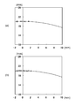
- FIG. 6 shows the change with time of the measured value when the resistivity was measured repeatedly 720 times in total. Since the rotational movement angle of the probe is performed every 1 °, the numerical value on the horizontal axis in FIG. 6 is the total of the rotational movement angles and is equal to the total number of measurements.
- FIG. 7 shows a change with time when a silicon single crystal wafer 10 having a diameter of 200 mm and a resistivity of 14.3 ⁇ ⁇ cm is used as a standard sample and the resistivity of the central portion thereof is repeatedly measured with a probe 1 having a probe interval of 1 mm.
- the numerical value on the horizontal axis in FIG. 7 means the number of measurements.
- the present invention is not limited to the above embodiment.
- the above-described embodiment is an example, and any object having substantially the same configuration as the technical idea described in the claims of the present invention and exhibiting the same effect and effect is the present invention. Is included in the technical scope of.
Landscapes
- Physics & Mathematics (AREA)
- General Physics & Mathematics (AREA)
- Measurement Of Resistance Or Impedance (AREA)
- Testing Or Measuring Of Semiconductors Or The Like (AREA)
Abstract
本発明は、シリコン単結晶からなる標準サンプルの測定面の抵抗率を四探針法により繰返し測定して抵抗率測定装置の管理を行う方法であって、前記標準サンプルとして、前記測定面がシリコンインゴットの中心軸に直交する平面であり、前記測定面の面内に前記シリコンインゴットの中心軸と前記中心軸に直交する平面の交点を含む前記標準サンプルを用い、前記四探針法で使用する4本の探針の配列方向が、前記交点と測定位置とを結ぶ直線に対し直交する方向となるように配置して、前記四探針法による前記抵抗率の測定を行い、前記測定を行う毎に、前記交点を回転中心として所定の回転角度で前記測定位置を回転移動する抵抗率測定装置の管理方法である。これにより、標準サンプルであるシリコン単結晶の繰返し抵抗率測定を安定化できる抵抗率測定装置の管理方法を提供する。
Description
本発明は抵抗率測定装置の管理方法に関し、より詳しくは、四探針法を用いてシリコン単結晶の抵抗率を繰り返し測定することにより、抵抗率測定装置を管理する方法に関する。
四探針法を用いてシリコン単結晶の抵抗率を測定する方法は、SEMI MF84-0312(Test Method for Measuring Resistivity of Silicon Wafers with an In-line Four-point Probe)、及び、JIS H 0602(シリコン単結晶及びシリコンウェーハの4探針法による抵抗率測定方法)に規定されている。
また、四探針法の測定に用いられる装置は、非特許文献1に記載されるNISTサンプルを用いて定期的に校正される。
特許文献1は、シリコン単結晶薄膜の抵抗率を四探針法により測定する抵抗率測定方法において、4本の探針の先端部が同一直線上で平坦になるまで予め摩耗させた探針を用いて、シリコン単結晶薄膜の抵抗率を測定することを提案している。シリコン単結晶の抵抗率測定に用いられる四探針法の探針は通常、タングステン・カーバイド等の丈夫な材質が用いられ、先端部の曲率半径が40μm程度の探針4本が1mmの等間隔に配列されている。
NIST Special Publication 260-131, 2006Ed. The Certification of 100mm Diameter Silicon Resistivity SRMs 2541 Through 2547 Using Dual-Configuration Four-Point Probe Measurements, 2006 Edition
シリコン単結晶の抵抗率を測定する四探針法の抵抗率測定装置を管理するため、同一のシリコン単結晶を標準サンプルとして同じ位置を毎日、決まった時刻に測定し、その測定値が管理基準内にあることを確認する。これを日常管理測定という。
ここで、標準サンプルとするシリコン単結晶とは、ウェーハ形状のみならず、1/4ウェーハ等の破片形状、短冊形状、チップ形状、ブロック形状などのシリコン単結晶が含まれる。
四探針法で使用される探針にはタングステン・カーバイド等の丈夫な材質が用いられているため、探針がシリコン単結晶表面に接触する度、該シリコン単結晶表面に探針跡が形成される。探針跡はクレータ状に形成され、その中心部が窪むと共に周辺部が盛り上がるため、探針跡の形成された同じ位置を測定し続けると、シリコン単結晶と探針の接触状態が悪くなり、測定バラツキが大きくなっていく。
抵抗率あるいはそのバラツキが所定の管理基準を超えると、日常管理用のシリコン単結晶を新しいものに交換する必要がある。そして、新しいシリコン単結晶を日常管理用の標準サンプルとして使用するためには、その標準サンプルを多数回測定し、その平均値と標準偏差から抵抗率とバラツキの新たな管理基準値を算出しなければならない。
従来は、抵抗率測定機のステージに標準サンプルを手で載せていたため、ステージ上の標準サンプル位置が微妙にずれ、標準サンプルに形成される針跡が重なる頻度が低かった。その結果、標準サンプルの同じ位置を測定し続けることに起因する抵抗率の漸増と、バラツキの増大が顕在化するまでの期間が比較的長かった。しかしながら、測定実施者により測定位置が異なったり、測定の都度測定位置が変わったりするなどの、管理できない測定位置の微妙なズレが生じること自体、測定を管理する上では、決して好ましいことではない。
一方、近年、抵抗率測定機の自動化が進み、サンプルが正確にアライメントされるようになったため、日常管理用標準サンプルが同じ位置で毎日測定される度、針跡も同じ位置に形成されるようになり、抵抗率の漸増と、測定バラツキの増大が短期間の内に顕在化するようになった。四探針法の抵抗率測定装置自体に問題がなくても、日常管理用標準サンプルに針跡が形成されることによる抵抗率の変動(漸増、測定バラツキの増大)が発生する。このような場合、抵抗率測定装置と日常管理用標準サンプルのどちらに問題があるのか切り分けが困難になったり、短期間のうちに日常管理用標準サンプルを交換する必要が生じるという問題があった。
本発明は上記課題を解決するためになされたものであり、標準サンプルであるシリコン単結晶の繰返し抵抗率測定を安定化できる抵抗率測定装置の管理方法を提供することを目的とする。
本発明は、上記目的を達成するためになされたものであり、シリコン単結晶からなる標準サンプルの測定面の抵抗率を四探針法により繰返し測定して抵抗率測定装置の管理を行う方法であって、前記標準サンプルとして、前記測定面がシリコンインゴットの中心軸に直交する平面であり、前記測定面の面内に前記シリコンインゴットの中心軸と前記中心軸に直交する平面の交点を含む前記標準サンプルを用い、前記四探針法で使用する4本の探針の配列方向が、前記交点と測定位置とを結ぶ直線に対し直交する方向となるように配置して、前記四探針法による前記抵抗率の測定を行い、前記測定を行う毎に、前記交点を回転中心として所定の回転角度で前記測定位置を回転移動する抵抗率測定装置の管理方法を提供する。
このような抵抗率測定装置の管理方法によれば、抵抗率の測定位置がシリコン単結晶インゴットの中心位置から等距離となり、実質的に同じ抵抗率の位置を測定することとなるため、測定位置を変えた場合であっても、同じ位置を繰り返し測定したときと同等の抵抗率を測定することとなる。測定の度に測定位置がずれて探針跡が重なる頻度が低減するため、標準サンプルのシリコン単結晶と探針の接触状態が良好に保たれる結果、長期間安定した繰返し測定が可能となる。また、同一の標準サンプルを長期にわたって使用できること(長寿命化)により、管理基準値の算出等の煩雑な作業を減らすことができる。
このとき、前記回転移動の前後の前記測定位置の間隔が、抵抗率測定時に前記探針が前記測定面に接触して形成される探針跡の直径以上、前記4本の探針の各探針間の間隔以下となるように、前記所定の回転角度を設定する抵抗率測定装置の管理方法とすることができる。
これにより、探針跡が重なる頻度を低減することができ、同一の標準サンプルを用いて、より多くの測定点の測定を行うことができ、より長期間にわたって安定した測定が可能となる。
このとき、1回目の測定位置の方向を0°としたとき、前記所定の回転角度の総和が少なくとも360°未満の範囲では、前記探針が前記測定面と接触して形成される探針跡が重ならないように、前記所定の回転角度、及び/又は、前記交点と前記測定位置との距離を設定する抵抗率測定装置の管理方法とすることができる。
これにより、より安定して抵抗率の測定を行うことができる。
このとき、前記標準サンプルとしてシリコン単結晶ウェーハを用い、該シリコン単結晶ウェーハの中心を前記回転中心とし、前記測定位置を前記シリコン単結晶ウェーハの前記中心から半径方向に半径の1/2以下の領域とする抵抗率測定装置の管理方法とすることができる。
上記のような領域は抵抗率がより安定している領域であり、このような領域に四探針を配置すれば、抵抗率をより安定して測定することができる。
本発明は、また、シリコン単結晶からなる標準サンプルの測定面の抵抗率を四探針法により繰返し測定して抵抗率測定装置の管理を行う方法であって、前記四探針法で使用する4本の探針を、標準サンプルの回転方向と平行に配列して、前記四探針法による前記抵抗率の測定を行い、前記測定を行う毎に、所定の回転角度で前記標準サンプルの測定位置を回転移動する抵抗率測定装置の管理方法を提供する。
本発明の抵抗率測定装置の管理方法によれば、測定の度に測定位置がずれて探針跡が重なる頻度が低減するため、標準サンプルのシリコン単結晶と探針の接触状態が良好に保たれる結果、長期間安定した繰り返し測定が可能となる。また、同一の標準サンプルを長期間にわたって使用できること(長寿命化)により、管理基準値の算出等の煩雑な作業を減らすことができる。
以上のように、本発明の抵抗率測定装置の管理方法によれば、測定の度に測定位置をずらすことで探針跡が重なる頻度が低減するので、標準サンプルのシリコン単結晶と探針の接触状態が良好に保たれる結果、長期間安定した繰返し測定が可能となる。
以下、本発明を詳細に説明するが、本発明はこれらに限定されるものではない。
上述のように、標準サンプルであるシリコン単結晶の繰返し抵抗率測定を安定化できる抵抗率測定装置の管理方法が求められていた。
本発明者らは、上記課題について鋭意検討を重ねた結果、シリコン単結晶からなる標準サンプルの測定面の抵抗率を四探針法により繰返し測定して抵抗率測定装置の管理を行う方法であって、前記標準サンプルとして、前記測定面がシリコンインゴットの中心軸に直交する平面であり、前記測定面の面内に前記シリコンインゴットの中心軸と前記中心軸に直交する平面の交点を含む前記標準サンプルを用い、前記四探針法で使用する4本の探針の配列方向が、前記交点と測定位置とを結ぶ直線に対し直交する方向となるように配置して、前記四探針法による前記抵抗率の測定を行い、前記測定を行う毎に、前記交点を回転中心として所定の回転角度で前記測定位置を回転移動する抵抗率測定装置の管理方法により、測定の度に測定位置がずれて探針跡が重なる頻度が低減するため、標準サンプルのシリコン単結晶と探針の接触状態が良好に保たれる結果、長期間にわたり安定した繰返し測定が可能となり、さらに、同一の標準サンプルを長期にわたって使用できること(長寿命化)が可能となり、管理基準値の算出等の煩雑な作業を減らすことができることを見出し、本発明を完成した。
以下、図面を参照して説明する。
本発明に係る抵抗率測定装置の管理方法においては、標準サンプルとして、測定面がシリコンインゴットの中心軸に直交する平面であり、測定面の面内にシリコンインゴットの中心軸と、中心軸に直交する平面の交点Cenを含むシリコン単結晶を用いる。このようなシリコン単結晶は、交点Cenを中心に周方向で一定の抵抗率分布を有している。このような標準サンプルは、シリコンインゴットの特性を反映して、交点Cenを中心とした半径r(rの数値は任意)の円の円周方向では、交点Cenを中心とした半径R方向よりも、抵抗率のバラツキが非常に小さい。したがって、このような標準サンプルを用い、四探針法で使用する4本の探針の配列方向が、交点Cenと測定位置とを結ぶ直線に対し直交する方向となるように配置して、周方向に測定位置をずらしながら抵抗率測定を行うことで、抵抗率の測定位置がシリコン単結晶インゴットの中心位置から等距離となり、実質的に同じ抵抗率の位置を測定することとなり、測定位置を変えた場合であっても、同じ位置を繰り返し測定したときと同等の抵抗率を測定することとなる。さらに、四探針法で使用する4本の探針の探針跡形成の影響を小さくして、安定して抵抗率測定管理を行うことができることを本発明者らは見出し、本発明を完成させた。
図1は、本発明に係る抵抗率測定装置の管理方法を含む概略工程図を示し、本発明に係る抵抗率測定装置の管理方法に用いられる標準サンプルのシリコン単結晶の準備方法の一例を含めて示す。まず、CZ法で引き上げられたインゴットの任意の位置より薄板状のウェーハをスライスする(図1(a)、シリコンインゴットのスライス工程)。スライスして現れる面が、インゴットの軸方向に対し直交する(垂直な)平面となるようにスライスする。ここで、インゴットの軸方向に対し直交する(垂直な)平面には、インゴットの軸方向に対し90°±10°の範囲内の平面を含む。
次に、スライスされたシリコン単結晶の主表面を#240~#2000番手で研削する(図1(b)、第1の研削工程)。高輝度平面研削を行う場合は、初めに#325程度の粗い砥石を用い粗研削して前記シリコン単結晶の厚さを調整した後、#1500以上の砥石を用いて研削し、所望の光沢度にする。
続いて、アンモニア(NH3)水・過酸化水素(H2O2)水、フッ化水素酸(HF)・過酸化水素(H2O2)水などを用いてシリコン単結晶を洗浄し(図1(c)、洗浄工程)、次工程のドナーキラー熱処理で用いられる熱処理炉が汚染されることを防止する。
ドナーキラー熱処理工程(図1(d))では、横型炉、縦型炉、あるいはRTP炉を用い、窒素ガス雰囲気中、650℃又は1100℃でシリコン単結晶を熱処理し、酸素ドナーを消去する。
前記ドナーキラー熱処理工程で、シリコン単結晶の表面に酸化膜が形成されるので、フッ化水素酸(HF)を用いて酸化膜を除去する(図1(e)、フッ酸処理工程)。ただし、この酸化膜は次の第2の研削工程で除去することができるので、省略することもできる。フッ化水素酸(HF)で処理することにより、確実に酸化膜を除去することができる。
前記ドナーキラー熱処理工程、あるいは前記フッ酸処理工程で、シリコン単結晶の表面が変質する。そこで、第2の研削工程(図1(f))を施し、変質したシリコン単結晶の表面を削り取ると共に研削面に戻す。高輝度平面研削を行う場合は、初めに#325程度の粗い砥石を用い粗研削して前記シリコン単結晶の厚さを調整した後、#1500以上の砥石を用いて研削し、所望の光沢度にする。表面が研削面のシリコン単結晶を四探針法で測定すると、探針端とシリコン単結晶表面の接触状態がより良好になるため、好ましい。
このようにして準備したシリコン単結晶を標準サンプルとして、シリコン単結晶の抵抗率保証や抵抗率測定装置の管理(図1(g)、抵抗率測定装置の管理工程)に用いる。抵抗率測定装置の管理方法としては、毎日行う日常管理と、例えば半年毎あるいは毎年行う校正があるが、どちらの管理方法でも同一のシリコン単結晶が標準サンプルとして繰り返し測定される。
本発明に係る抵抗率測定装置の管理方法で使用可能な標準サンプルのシリコン単結晶は、ウェーハ形状のみならず、1/4ウェーハ等の破片形状、短冊形状、チップ形状、ブロック形状などのシリコン単結晶を含むが、ウェーハ形状のシリコン単結晶がその中心を特定し易いので、最も好適に用いられる。
図2は、本発明に係る四探針法を用いた抵抗率測定装置の管理方法の概略説明図である。四探針抵抗率測定は、4本の探針が一直線上に等間隔sに並べられたプローブ1を有し、該プローブ1を駆動手段(不図示)により上下して探針2a,2b,2c,2dの先端をシリコン単結晶10の表面に当接させるとともに、探針2aと探針2dの間に所定の電流Iを印加しつつ、探針2bと探針2cの間で電圧Vを測ることにより、抵抗率ρを求める。十分に大きな面積と厚さを有するウェーハ形状のシリコン単結晶の中心部を、温度補正無しで測定する場合、抵抗率ρは、式(1)で求められる。
ρ=2πsV/I ・・・ (1)
ρ=2πsV/I ・・・ (1)
より具体的には、探針2a,2b,2c,2dは、タングステン・カーバイド等の丈夫な材質が用いられ、先端部の曲率半径が略40μmの探針4本が1mmの等間隔に配列され、200g/本の針圧でシリコン単結晶10の表面に当接する。探針2a,2b,2c,2dが当接したシリコン単結晶10の表面には、直径略20μmの探針跡3(3a,3b,3c,3d)が形成される。
探針跡3はクレータ状に形成され、その中心部が窪むと共に周辺部が盛り上がるため、探針跡3の形成された同一シリコン単結晶の同じ位置を抵抗率測定し続けると、シリコン単結晶10と探針2a,2b,2c,2dの接触状態が悪くなり、抵抗率が漸増するとともに測定バラツキが大きくなっていく。
そこで、図3に示すように、標準サンプルとしての同一シリコン単結晶10の抵抗率を四探針法により繰返し測定する際、4本の探針2a,2b,2c,2dが配列された方向が、交点Cenと測定位置とを結ぶ直線に対し直交する方向となるように配置して、交点Cenを中心としてシリコン単結晶10を所定角度ずつ自転させながら、一定の間隔で抵抗率測定を行う。言い換えると、4本の探針2a,2b,2c,2dが配列された方向が、交点Cenを中心とした半径rの円の接線方向、すなわち、標準サンプルの回転方向となるように配置して、半径rの円周に沿って、一定の間隔で抵抗率測定させる。このようにすると、シリコン単結晶10の表面に、半径rの円状に探針跡3が形成される。なお、測定位置の変更は、探針と標準サンプルとを相対移動させればよく、標準サンプルを固定して、探針を移動させてもよいことは言うまでもない。
一例として、図4(a),(b)及び図5(a),(b)に、シリコン単結晶10を1回の測定毎に1.63°間隔で自転させることにより、探針間隔1mmのプローブ1が、半径20mmの円周に沿って、0.57mm間隔で繰返し抵抗率測定させる場合に形成する円状の探針跡3を示す。ここで、探針跡3aを「○」、探針跡3bを「×」、探針跡3cを「△」、探針跡3dを「+」で表示する。なお、図4、図5ともに、図の縦軸及び横軸は、シリコン単結晶10(シリコン単結晶ウェーハ)の中心からの距離を示す。
図4(a)は初回測定時の探針跡であり、シリコン単結晶10が未だ自転していないので、探針跡3(3a,3b,3c,3d)の真ん中が座標(0,20)に位置する。なお、探針跡3が図4(a)に示されるような位置関係になるように、探針2a,2b,2c,2dの間隔が設定された場合、各探針2a,2b,2c,2dは直線状に配置されているため、厳密には、交点Cenから各探針跡3(3a,3b,3c,3d)への距離は異なる。具体的には、交点Cenから探針跡3a,3dへの距離と、交点Cenから探針跡3b,3cへの距離とは、異なる。しかし、この距離差は非常に小さく、実質的に同一抵抗率とみなすことができる。
図4(b)は探針2a,2b,2c,2dが配列された方向に、シリコン単結晶10が図4(a)から1.63°時計回りに自転した後に抵抗率測定した結果、シリコン単結晶10の表面に形成される探針跡3を示す。この時、各探針跡3a,3b,3c,3dは、初回測定時の探針跡からそれぞれ0.57mm離れた位置に形成される。
図5(a)は探針2a,2b,2c,2dが配列された方向に、シリコン単結晶10が図4(b)からさらに1.63°時計回りに自転した後に抵抗率測定した結果、シリコン単結晶10の表面に形成される探針跡3を示す。この時、各探針跡3a,3b,3c,3dは、図4(b)の探針跡からそれぞれ0.57mm離れた位置に形成される。そして、探針跡3aと3b、探針跡3bと3c、探針跡3cと3dはそれぞれ接近して形成されるが、略140μm離れており、同一箇所を繰り返し測定することにはならない。
図5(b)は探針2a,2b,2c,2dが配列された方向に、シリコン単結晶10が初回測定の図4(a)から1.63°間隔で時計回りに24.45°自転した結果、シリコン単結晶10の表面に形成される探針跡3a,3b,3c,3dを示す。図5(a)と同様、探針跡3aと3b、探針跡3bと3c、探針跡3cと3dはそれぞれ接近して形成されるが、略140μm離れており、互いに接触しないので同一箇所を繰り返し測定することにはならない。
図5(b)に示される探針跡3a,3b,3c,3dの位置関係は、探針2a,2b,2c,2dが円を1周する間、変化しない。つまり、例えば、測定位置を移動する間隔を1.63°、円の半径rを20mmに設定することにより、探針間隔1mmの四探針測定用プローブ1の探針2a,2b,2c,2dが0.57mm間隔で円周を1周する間、探針跡3a,3b,3c,3dが重なって形成されないようにすることができる。
言い換えると、1回目の測定位置の方向を0°としたとき、測定位置を回転移動する所定の回転角度の総和が少なくとも360°未満の範囲では、探針が測定面と接触して形成される探針跡が重ならないように、所定の回転角度、及び/又は、交点Cenと前記測定位置との距離を設定することが好ましい。これは、標準サンプルのシリコン単結晶10として、円形のシリコン単結晶ウェーハを使用する場合には、探針がシリコン単結晶ウェーハの面内で少なくとも1周する間、探針跡が重なって形成されないように設定することが好ましいことを意味する。また、円形ではない例えば1/4ウェーハ形状などのシリコン単結晶を使用する場合には、交点Cenを中心に円弧を描くように測定位置を回転移動する時の1巡目の回転角度の総和は90°未満であり、1巡目の測定時に探針跡が重なって形成されないように設定することが好ましいことを意味する。このように測定位置の設定を行うことで、より安定して抵抗率の測定を行うことができる。
また、測定位置を回転移動する前後の測定位置の間隔は、探針跡の直径以上、4本の探針の各探針間の間隔以下となるように、所定の回転角度を設定することが好ましい。このように設定すると、同一の標準サンプルを用いて、より多くの測定点の測定を行うことができ、より長期間にわたって安定した測定が可能となる。上記の例では、測定位置を移動する間隔0.57mmは、探針2a,2b,2c,2dがシリコン単結晶10の表面に接触して形成する探針跡3a,3b,3c,3dの各直径20μmより長く、前記探針間の間隔1mmより短くなるように設定されている。
シリコン単結晶10がシリコン単結晶ウェーハの場合、シリコン単結晶ウェーハ10の中心は、探針2a,2b,2c,2dが1周する円の中心(交点Cen)となる。この場合、前記円の半径rを前記シリコン単結晶ウェーハの半径の1/2以下とすると、抵抗率測定値が外周の影響を受けないので好ましい。また、前記円周の半径rの下限値は特に限定されないが、例えば5mmとすることができる。
測定位置を移動する間隔を、例えば、探針跡3a,3b,3c,3dの各直径20μmと同じ20μmにすることもできる。この場合、探針2dが先頭で右方向(時計回り)に進むとして、探針2a,2b,2cは最初の50回の繰返し測定の間、探針跡に接触せずに繰返し測定できるが、その後は、探針跡に接触しつつ測定することになる。そのような場合でも、円周を1周する間に探針2aが接触する探針跡は最大でも3回測定分なので、探針跡から受ける影響がほとんどない。
一方、測定位置を移動する間隔を例えば、探針2a,2b,2c,2dの間隔と同じ1mmにすることもできる。この場合、探針2dが先頭で右方向(時計回り)に進むとして、探針2a,2b,2cは初回を除き、探針跡に接触しつつ測定することになる。それでも、円周を1周する間に探針2aが接触する探針跡は最大でも3回測定分なので、探針跡から受ける影響がほとんどない。
測定間隔を例えば、探針2a,2b,2c、2dの間隔よりも大きくすることもできる。しかしこの場合、探針2a,2b,2c、2dが円周を1周する間にできる繰返し測定の回数が少なくなってしまうため、測定間隔は小さい方が好ましい。
以下、実施例を挙げて本発明について詳細に説明するが、これは本発明を限定するものではない。
[実施例1]
直径200mm、抵抗率12.2Ω・cmのシリコン単結晶ウェーハ10を標準サンプルとして用い、探針間隔1mmのプローブ1を半径20mmの円周に沿うように1°(0.35mm)間隔で2周、合計720回繰返し抵抗率測定した場合の測定値の経時変化を図6に示す。なお、探針の回転移動の角度を1°毎に行っているため、図6の横軸の数値は、移動を行った回転角度の総和であり、かつ、測定回数の合計に等しい。
直径200mm、抵抗率12.2Ω・cmのシリコン単結晶ウェーハ10を標準サンプルとして用い、探針間隔1mmのプローブ1を半径20mmの円周に沿うように1°(0.35mm)間隔で2周、合計720回繰返し抵抗率測定した場合の測定値の経時変化を図6に示す。なお、探針の回転移動の角度を1°毎に行っているため、図6の横軸の数値は、移動を行った回転角度の総和であり、かつ、測定回数の合計に等しい。
図6に示すように、半径20mmの円周に沿って探針2a,2b,2c,2dが2周したにも関わらず、抵抗率の経時変化のバラツキは極めて小さかった。2周の間の抵抗率バラツキを下記式(2)で求めると、±0.37%であった。
抵抗率バラツキ
=±(最大値-最小値)/(最大値+最小値)×100(%)
・・・(2)
抵抗率バラツキ
=±(最大値-最小値)/(最大値+最小値)×100(%)
・・・(2)
[比較例1]
直径200mm、抵抗率14.3Ω・cmのシリコン単結晶ウェーハ10を標準サンプルとして用い、探針間隔1mmのプローブ1でその中心部を繰返し抵抗率測定した場合の経時変化を図7に示す。図7の横軸の数値は、測定回数を意味する。
直径200mm、抵抗率14.3Ω・cmのシリコン単結晶ウェーハ10を標準サンプルとして用い、探針間隔1mmのプローブ1でその中心部を繰返し抵抗率測定した場合の経時変化を図7に示す。図7の横軸の数値は、測定回数を意味する。
図7に示すように、中心部を繰返し233回抵抗率測定した場合、その間の抵抗率バラツキを上記式(2)で求めると、±0.84%であった。
実施例1と比較例1の結果の比較から明らかなように、本発明に係る抵抗率測定装置の管理方法を採用した場合、測定した抵抗率の測定間のバラツキを極めて小さくすることが可能となった。
なお、本発明は、上記実施形態に限定されるものではない。上記実施形態は例示であり、本発明の特許請求の範囲に記載された技術的思想と実質的に同一な構成を有し、同様な作用効果を奏するものは、いかなるものであっても本発明の技術的範囲に包含される。
Claims (5)
- シリコン単結晶からなる標準サンプルの測定面の抵抗率を四探針法により繰返し測定して抵抗率測定装置の管理を行う方法であって、
前記標準サンプルとして、前記測定面がシリコンインゴットの中心軸に直交する平面であり、前記測定面の面内に前記シリコンインゴットの中心軸と前記中心軸に直交する平面の交点を含む前記標準サンプルを用い、
前記四探針法で使用する4本の探針の配列方向が、前記交点と測定位置とを結ぶ直線に対し直交する方向となるように配置して、前記四探針法による前記抵抗率の測定を行い、
前記測定を行う毎に、前記交点を回転中心として所定の回転角度で前記測定位置を回転移動することを特徴とする抵抗率測定装置の管理方法。 - 前記回転移動の前後の前記測定位置の間隔が、抵抗率測定時に前記探針が前記測定面に接触して形成される探針跡の直径以上、前記4本の探針の各探針間の間隔以下となるように、前記所定の回転角度を設定することを特徴とする請求項1に記載の抵抗率測定装置の管理方法。
- 1回目の測定位置の方向を0°としたとき、前記所定の回転角度の総和が少なくとも360°未満の範囲では、前記探針が前記測定面と接触して形成される探針跡が重ならないように、前記所定の回転角度、及び/又は、前記交点と前記測定位置との距離を設定することを特徴とする請求項1又は請求項2に記載の抵抗率測定装置の管理方法。
- 前記標準サンプルとしてシリコン単結晶ウェーハを用い、該シリコン単結晶ウェーハの中心を前記回転中心とし、前記測定位置を前記シリコン単結晶ウェーハの前記中心から半径方向に半径の1/2以下の領域とすることを特徴とする請求項1から請求項3のいずれか1項に記載の抵抗率測定装置の管理方法。
- シリコン単結晶からなる標準サンプルの測定面の抵抗率を四探針法により繰返し測定して抵抗率測定装置の管理を行う方法であって、
前記四探針法で使用する4本の探針を、標準サンプルの回転方向と平行に配列して、前記四探針法による前記抵抗率の測定を行い、
前記測定を行う毎に、所定の回転角度で前記標準サンプルの測定位置を回転移動することを特徴とする抵抗率測定装置の管理方法。
Applications Claiming Priority (2)
| Application Number | Priority Date | Filing Date | Title |
|---|---|---|---|
| JP2019-104674 | 2019-06-04 | ||
| JP2019104674A JP7205391B2 (ja) | 2019-06-04 | 2019-06-04 | 抵抗率測定装置の管理方法 |
Publications (1)
| Publication Number | Publication Date |
|---|---|
| WO2020246138A1 true WO2020246138A1 (ja) | 2020-12-10 |
Family
ID=73649765
Family Applications (1)
| Application Number | Title | Priority Date | Filing Date |
|---|---|---|---|
| PCT/JP2020/016069 Ceased WO2020246138A1 (ja) | 2019-06-04 | 2020-04-10 | 抵抗率測定装置の管理方法 |
Country Status (2)
| Country | Link |
|---|---|
| JP (1) | JP7205391B2 (ja) |
| WO (1) | WO2020246138A1 (ja) |
Citations (1)
| Publication number | Priority date | Publication date | Assignee | Title |
|---|---|---|---|---|
| JP2011211060A (ja) * | 2010-03-30 | 2011-10-20 | Hitachi Kokusai Denki Engineering:Kk | 半導体ウェーハ抵抗率測定装置 |
Family Cites Families (1)
| Publication number | Priority date | Publication date | Assignee | Title |
|---|---|---|---|---|
| JP2001274211A (ja) | 2000-03-27 | 2001-10-05 | Shin Etsu Handotai Co Ltd | 抵抗率測定方法 |
-
2019
- 2019-06-04 JP JP2019104674A patent/JP7205391B2/ja active Active
-
2020
- 2020-04-10 WO PCT/JP2020/016069 patent/WO2020246138A1/ja not_active Ceased
Patent Citations (1)
| Publication number | Priority date | Publication date | Assignee | Title |
|---|---|---|---|---|
| JP2011211060A (ja) * | 2010-03-30 | 2011-10-20 | Hitachi Kokusai Denki Engineering:Kk | 半導体ウェーハ抵抗率測定装置 |
Also Published As
| Publication number | Publication date |
|---|---|
| JP7205391B2 (ja) | 2023-01-17 |
| JP2020198383A (ja) | 2020-12-10 |
Similar Documents
| Publication | Publication Date | Title |
|---|---|---|
| US7500902B2 (en) | Thickness-measuring method during grinding process | |
| CN106133209B (zh) | 碳化硅单晶衬底、碳化硅外延衬底及它们的制造方法 | |
| TWI580500B (zh) | Workpiece cutting method and workpiece to maintain a rule | |
| JP5837290B2 (ja) | エピタキシャルウェーハの製造方法及びエピタキシャル成長装置 | |
| CN101168851A (zh) | 硅外延片及其制造方法 | |
| KR102081379B1 (ko) | 면취 가공 장치 및 노치리스 웨이퍼의 제조 방법 | |
| KR20210134633A (ko) | 실리콘 단결정의 저항률 측정방법 | |
| CN106663597B (zh) | Soi晶圆的制造方法 | |
| JP5499383B2 (ja) | 半導体ウェーハ抵抗率測定装置 | |
| JP5867377B2 (ja) | 円筒研削機および単結晶ウエーハの製造方法 | |
| US20100048034A1 (en) | Vertical boat for heat treatment and heat treatment method of semiconductor wafer using thereof | |
| JP7205391B2 (ja) | 抵抗率測定装置の管理方法 | |
| JP7207214B2 (ja) | 抵抗率測定装置の管理方法 | |
| US20240413022A1 (en) | Substrate processing method and substrate processing system | |
| CN113119327A (zh) | 能够改善<111>晶向晶棒切割warp值的定向多线切割方法 | |
| JP7240827B2 (ja) | 原料結晶の抵抗率の測定方法及びfzシリコン単結晶の製造方法 | |
| TWI737339B (zh) | 單結晶矽的電阻率測定方法 | |
| CN112485290B (zh) | 晶片结晶定向的估测方法与系统 | |
| JP2011014800A (ja) | エピタキシャル層の膜厚測定方法、エピタキシャルウェーハの製造方法およびエピタキシャルウェーハの製造工程管理方法 | |
| KR100526215B1 (ko) | 실리콘 단결정 웨이퍼의 제조방법 및 제조장치 | |
| KR20140090809A (ko) | 서셉터 지지부를 구비하는 웨이퍼 에피택셜 성장 장치 | |
| JP6056749B2 (ja) | エピタキシャル成長前後の半導体ウェーハのエッジ形状の評価方法 | |
| KR20070111511A (ko) | 반도체 웨이퍼 지지용 그리퍼와 지지 방법 및 형상 측정장치 | |
| JP6766792B2 (ja) | 検査治具及びこれを用いたシリコンウェーハの欠陥検査方法 | |
| JP2003197546A (ja) | 熱処理装置およびシリコンエピタキシャルウェーハの製造方法 |
Legal Events
| Date | Code | Title | Description |
|---|---|---|---|
| 121 | Ep: the epo has been informed by wipo that ep was designated in this application |
Ref document number: 20819536 Country of ref document: EP Kind code of ref document: A1 |
|
| NENP | Non-entry into the national phase |
Ref country code: DE |
|
| 122 | Ep: pct application non-entry in european phase |
Ref document number: 20819536 Country of ref document: EP Kind code of ref document: A1 |