WO2020241108A1 - 固体撮像素子 - Google Patents
固体撮像素子 Download PDFInfo
- Publication number
- WO2020241108A1 WO2020241108A1 PCT/JP2020/016736 JP2020016736W WO2020241108A1 WO 2020241108 A1 WO2020241108 A1 WO 2020241108A1 JP 2020016736 W JP2020016736 W JP 2020016736W WO 2020241108 A1 WO2020241108 A1 WO 2020241108A1
- Authority
- WO
- WIPO (PCT)
- Prior art keywords
- voltage
- unit
- shared
- solid
- current
- Prior art date
- Legal status (The legal status is an assumption and is not a legal conclusion. Google has not performed a legal analysis and makes no representation as to the accuracy of the status listed.)
- Ceased
Links
Images






Classifications
-
- H—ELECTRICITY
- H04—ELECTRIC COMMUNICATION TECHNIQUE
- H04N—PICTORIAL COMMUNICATION, e.g. TELEVISION
- H04N25/00—Circuitry of solid-state image sensors [SSIS]; Control thereof
- H04N25/50—Control of the SSIS exposure
-
- H—ELECTRICITY
- H04—ELECTRIC COMMUNICATION TECHNIQUE
- H04N—PICTORIAL COMMUNICATION, e.g. TELEVISION
- H04N25/00—Circuitry of solid-state image sensors [SSIS]; Control thereof
- H04N25/40—Extracting pixel data from image sensors by controlling scanning circuits, e.g. by modifying the number of pixels sampled or to be sampled
- H04N25/46—Extracting pixel data from image sensors by controlling scanning circuits, e.g. by modifying the number of pixels sampled or to be sampled by combining or binning pixels
-
- H—ELECTRICITY
- H04—ELECTRIC COMMUNICATION TECHNIQUE
- H04N—PICTORIAL COMMUNICATION, e.g. TELEVISION
- H04N25/00—Circuitry of solid-state image sensors [SSIS]; Control thereof
- H04N25/47—Image sensors with pixel address output; Event-driven image sensors; Selection of pixels to be read out based on image data
-
- H—ELECTRICITY
- H04—ELECTRIC COMMUNICATION TECHNIQUE
- H04N—PICTORIAL COMMUNICATION, e.g. TELEVISION
- H04N25/00—Circuitry of solid-state image sensors [SSIS]; Control thereof
- H04N25/70—SSIS architectures; Circuits associated therewith
-
- H—ELECTRICITY
- H10—SEMICONDUCTOR DEVICES; ELECTRIC SOLID-STATE DEVICES NOT OTHERWISE PROVIDED FOR
- H10F—INORGANIC SEMICONDUCTOR DEVICES SENSITIVE TO INFRARED RADIATION, LIGHT, ELECTROMAGNETIC RADIATION OF SHORTER WAVELENGTH OR CORPUSCULAR RADIATION
- H10F39/00—Integrated devices, or assemblies of multiple devices, comprising at least one element covered by group H10F30/00, e.g. radiation detectors comprising photodiode arrays
- H10F39/10—Integrated devices
- H10F39/12—Image sensors
Definitions
- the present disclosure relates to an asynchronous solid-state image sensor.
- a synchronous solid-state image sensor that images image data (frames) in synchronization with a synchronization signal such as a vertical synchronization signal has been used in an image pickup device or the like.
- image data can be acquired only every synchronization signal cycle (for example, 1/60 second), so that faster processing can be performed in fields related to transportation and robots. It becomes difficult to respond when requested. Therefore, an asynchronous solid-state image sensor has been proposed for each pixel address, in which a detection circuit for detecting in real time that the amount of light of the pixel exceeds a threshold value as an address event is provided for each pixel (for example, Patent Document 1). reference.).
- Such a solid-state image sensor that detects an address event for each pixel is called a DVS (Dynamic Vision Sensor).
- the above-mentioned asynchronous solid-state image sensor (that is, DVS) can generate and output data at a much higher speed than the synchronous solid-state image sensor. Therefore, for example, in the field of transportation, it is possible to improve safety by executing a process of recognizing an image of a person or an obstacle at high speed.
- the address event detection circuit has a problem that the number of elements such as transistors is larger than that of the synchronous pixel circuit, and the power consumption is increased.
- An object of the present disclosure is to provide a solid-state image sensor capable of reducing power consumption.
- the solid-state imaging device includes a photoelectric conversion element that photoelectrically converts incident light to generate a current, a current-voltage conversion unit that converts the current input from the photoelectric conversion element into a voltage, and the current-voltage conversion unit. It is provided with a plurality of subtraction units which are connected to and subtract the other voltage from one voltage input from the current-voltage conversion unit at different timings.
- the solid-state imaging device is connected to a plurality of photoelectric conversion elements, each of which photoelectrically converts incident light to generate a current, and one to each of the plurality of photoelectric conversion elements, and is input from the photoelectric conversion element. From a plurality of current-voltage converters that convert the current into a voltage and a first voltage based on one voltage that is connected to the plurality of current-voltage converters and input from each of the current-voltage converters at different timings. It includes a shared subtraction unit that subtracts a second voltage based on the other voltage.
- FIG. 1 is a block diagram showing a configuration example of an image pickup apparatus 100 according to each embodiment of the present disclosure.
- the image pickup device 100 includes an image pickup lens 110, a solid-state image sensor 200, a recording unit 120, and a control unit 130.
- the image pickup device 100 a camera mounted on an industrial robot, an in-vehicle camera, or the like is assumed.
- the image pickup lens 110 collects the incident light and guides it to the solid-state image sensor 200.
- the solid-state image sensor 200 captures image data by photoelectrically converting incident light.
- the solid-state image sensor 200 executes predetermined signal processing such as image recognition processing on the imaged image data, and stores data indicating the processing result and an address event detection signal in the recording unit 120. It is output via the signal line 209.
- the recording unit 120 records data from the solid-state image sensor 200.
- the control unit 130 controls the solid-state image sensor 200 to capture image data.
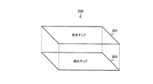
- FIG. 2 is a diagram showing an example of a laminated structure of the solid-state image sensor 200.
- the solid-state imaging device 200 includes a detection chip 202 and a light receiving chip 201 laminated on the detection chip 202.
- the detection chip 202 and the light receiving chip 201 are electrically connected via a connection portion such as a via. In addition to vias, it can also be connected by Cu-Cu bonding or bumps.
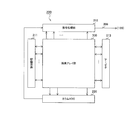
- FIG. 3 is a block diagram showing a configuration example of the solid-state image sensor 200 according to each embodiment of the present disclosure.
- the solid-state image sensor 200 includes a drive circuit 211, a signal processing unit 212, an arbiter 213, a column ADC 220, and a pixel array unit 300.
- a plurality of pixels are arranged in a two-dimensional grid pattern in the pixel array unit 300. Further, the pixel array unit 300 is divided into a plurality of pixel blocks, each of which is composed of a predetermined number of pixels.
- a set of pixels or pixel blocks arranged in the horizontal direction is referred to as a "row”
- a set of pixels or pixel blocks arranged in a direction perpendicular to the row is referred to as a "column”.
- Each pixel generates an analog signal with a voltage corresponding to the photocurrent as a pixel signal.
- each of the pixels detects the presence or absence of an address event depending on whether or not the amount of change in the photocurrent exceeds a predetermined threshold value. Then, when the address event occurs, the pixel block outputs the request to the arbiter.
- the pixel block is configured to exert a different function for each embodiment. The function of the pixel block will be described later.
- the drive circuit 211 drives each of the pixels to output a pixel signal to the column ADC 220.
- the arbiter 213 arbitrates the request from each pixel and transmits the response to the pixel based on the arbitration result.
- the pixel that receives the response supplies the detection signal indicating the detection result to the drive circuit 211 and the signal processing unit 212.
- the column ADC 220 converts an analog pixel signal from a row of pixel blocks into a digital signal for each row of pixel blocks.
- the column ADC 220 supplies a digital signal to the signal processing unit 212.
- the signal processing unit 212 executes predetermined signal processing such as CDS (Correlated Double Sampling) processing and image recognition processing on the digital signal from the column ADC 220.
- the signal processing unit 212 supplies the data indicating the processing result and the detection signal to the recording unit 120 via the signal line 209.
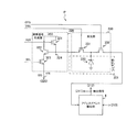
- FIG. 4 is a circuit diagram showing a configuration example of the pixel P in each embodiment of the present disclosure.
- the pixel array unit 300 has a plurality of pixels P arranged in m rows ⁇ n columns (m and n are natural numbers).
- the plurality of pixels P are arranged in a pixel array unit 300, for example, in a matrix.
- the pixel P includes a pixel signal generation unit 320, a light receiving unit 330, and an address event detection unit 4.
- a vertical signal line VSL is wired for each row of pixels P. Assuming that the number of columns of the pixel P is n (n is a natural number), n vertical signal lines VSL are arranged.
- the light receiving unit 330 photoelectrically converts the incident light to generate a photocurrent.
- the light receiving unit 330 supplies an photocurrent to either the pixel signal generation unit 320 or the address event detection unit 4 according to the control of the drive circuit 211.
- the pixel signal generation unit 320 generates a signal having a voltage corresponding to the photocurrent as a pixel signal SIG.
- the pixel signal generation unit 320 supplies the generated pixel signal SIG to the column ADC 220 via the vertical signal line VSL.
- the address event detection unit 4 detects the presence or absence of an address event depending on whether or not the amount of change in the photocurrent from the light receiving unit 330 exceeds a predetermined threshold value.
- the address event is, for example, an on-event indicating that the amount of change in photocurrent exceeds (exceeds) the upper limit threshold value and an off-event indicating that the amount of change in photocurrent exceeds (below) the lower threshold value. Consists of.
- the address event detection signal is composed of, for example, one bit indicating an on-event detection result and one bit indicating an off-event detection result.
- the address event detection unit 4 can also detect only on-events.
- the address event detection unit 4 supplies the arbiter 213 with a request for transmitting a detection signal. Then, when the response to the request is received from the arbiter 213, the address event detection unit 4 supplies the detection signal to the drive circuit 211 and the signal processing unit 212.
- the pixel signal generation unit 320 includes a reset transistor 321, an amplification transistor 322, a selection transistor 323, and a floating diffusion layer 324.
- the light receiving unit 330 is connected to the address event detection unit 4.
- the light receiving unit 330 includes a transfer transistor 331, an OFG (Over Flow Gate) transistor 332, and a photoelectric conversion element 333.
- the transfer transistor 331, the OFG transistor 332, and the photoelectric conversion element 333 are arranged for each pixel P.
- the transfer signal TRG is supplied to the transfer transistor 331 by the drive circuit 211 (see FIG. 3).
- a control signal OFG is supplied to the OFG transistor 332 by the drive circuit 211.
- an N-type MOS (Metal-Oxide-Semiconductor) transistor is used as the reset transistor 321 and the amplification transistor 322 and the selection transistor 323, for example.
- an N-type MOS transistor is used for the transfer transistor 331 and the OFG transistor 332.
- each of the photoelectric conversion elements 333 is arranged on the light receiving chip 201 (see FIG. 2). All of the elements other than the photoelectric conversion element 333 are arranged on the detection chip 202 (see FIG. 2).
- the photoelectric conversion element 333 photoelectrically converts the incident light to generate an electric charge.
- the transfer transistor 331 transfers an electric charge from the corresponding photoelectric conversion element 333 to the floating diffusion layer 324 according to the transfer signal TRG.
- the OFG transistor 332 supplies the electric signal generated by the corresponding photoelectric conversion element 333 to the address event detection unit 4 according to the control signal OFG.
- the supplied electric signal is a photocurrent composed of electric charges.
- the floating diffusion layer 324 accumulates electric charges and generates a voltage according to the amount of the accumulated electric charges.
- the reset transistor 321 initializes the charge amount of the floating diffusion layer 324 according to the reset signal from the drive circuit 211.
- the amplification transistor 322 amplifies the voltage of the floating diffusion layer 324.
- the selection transistor 323 outputs a signal of the amplified voltage as a pixel signal SIG to the column ADC 220 (see FIG. 3) via the vertical signal line VSL according to the selection signal SEL from the drive circuit 211.
- the drive circuit 211 drives the OFG transistors 332 of all pixels P by the control signal OFG to supply an photocurrent. As a result, the photocurrent of the light receiving unit 330 of the pixel P is supplied to the address event detection unit 4.
- the drive circuit 211 turns off the OFG transistor 332 of the pixel P and stops the supply of the photocurrent to the address event detection unit 4.
- the drive circuit 211 drives each transfer transistor 331 in order by the transfer signal TRG to transfer the electric charge to the plankton diffusion layer 324.
- the pixel signals of the plurality of pixels in the pixel block 310 are sequentially output.
- the solid-state image sensor 200 outputs only the pixel signal of the pixel P in which the address event is detected to the column ADC 220.
- the power consumption of the solid-state image sensor 200 and the amount of image processing can be reduced as compared with the case where the pixel signals of all the pixels are output regardless of the presence or absence of the address event.
- a light emitting device such as a lighting device or a display device installed indoors
- dynamic lighting pulse lighting or duty lighting
- these devices have flicker (fine).
- a light-dark (flicker) phenomenon may occur.
- the solid-state image sensor is used indoors, the light and darkness caused by this flicker phenomenon may be erroneously detected as an address event. As a result, the solid-state image sensor may reduce the detection accuracy of the address event.
- the solid-state image sensor according to the present embodiment is characterized in that deterioration in detection accuracy of address events due to the flicker phenomenon can be suppressed.
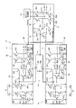
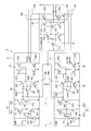
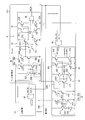
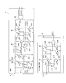
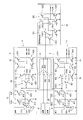
- FIG. 5 is a circuit block diagram showing a configuration example of an address event detection unit 4 and a flicker detection circuit 5 provided in the solid-state image sensor 200 according to the first embodiment. Note that in FIG. 5, the pixel signal generation unit 320, the transfer transistor 331, and the OFG transistor 332 provided in the pixel P are not shown.
- the solid-state image sensor 200 includes a plurality of address event detection units 4, an addition unit 6 connected to the plurality of address event detection units 4, and a flicker detection circuit 5 connected to the addition unit 6. It has.
- the number k of the address event detection unit 4 connected to the addition unit 6 and the flicker detection circuit 5 is a natural number equal to or less than the total number of pixels P (m ⁇ n) arranged in the pixel array unit 300.
- the address event detection unit 4 is formed for each pixel P. Therefore, the solid-state image sensor 200 according to the present embodiment includes (m ⁇ n) / k addition units 6 and a flicker detection circuit 5.
- the address event detection unit 4 provided in each of the pixels P provided in the solid-state imaging device 200 has the same configuration.
- the address event detection unit 4 includes a current-voltage conversion unit 41, a subtractor (an example of an individual subtraction unit) 430, a quantizer (an example of a determination unit) 43, and a transfer unit (not shown).
- the current-voltage conversion unit 41 has a logarithmic conversion circuit 41a and a buffer circuit 41b.
- the solid-state imaging device 200 includes a plurality of photoelectric conversion elements 333 (two are shown in FIG. 5), each of which photoelectrically converts incident light to generate an electric current. Further, the solid-state image sensor 200 is connected to each of the plurality of photoelectric conversion elements 333 one by one and converts the current input from the photoelectric conversion element 333 into a voltage (two are shown in FIG. 5).
- the current-voltage conversion unit 41 is provided.
- the current-voltage conversion unit 41 has a logarithmic conversion circuit 41a and a buffer circuit 41b.
- the current-voltage conversion unit 41 is configured to convert the current (photocurrent) input from the photoelectric conversion element 333 in the logarithmic conversion circuit 41a into a voltage value of logarithmic output.
- the buffer circuit 41b has a source follower type configuration and is configured to perform impedance conversion.
- the solid-state image sensor 200 is connected to each of the plurality of current-voltage conversion units 41 one by one, and is input from the connected current-voltage conversion unit 41 at different timings from the current-voltage conversion unit 41.
- An individual subtractor (an example of an individual subtraction unit) 42 for subtracting the other voltage from one voltage is provided.
- the individual subtractor 42 is configured to output a voltage difference from the voltage at the timing when the row drive signal from the drive circuit 211 (see FIG. 3) is switched from the on state to the off state.
- the quantizer 43 is configured to quantize the voltage signal input from the individual subtractor 42 into a digital signal and output it to the transfer unit as a detection signal (+) and a detection signal (-) using two thresholds. Has been done.
- the transfer unit is configured to transfer the detection signal (+) and the detection signal (-) input from the quantizer 43 to the signal processing unit 212 or the like.
- the transfer unit supplies the arbiter 213 with a request to transmit the detection signal.
- the transfer unit 450 receives the response to the request from the arbiter 213, the transfer unit 450 supplies the detection signal (+) and the detection signal ( ⁇ ) to the drive circuit 211 and the signal processing unit 212.
- the logarithmic conversion circuit 41a constituting the current-voltage conversion unit 41 includes an N-type transistor 411, an N-type transistor 413, a P-type transistor 412, and a capacitor C41.
- these transistors for example, MOS transistors are used.
- the source of the N-type transistor 411 is connected to the cathode of the photoelectric conversion element 333.
- the drain of the N-type transistor 411 is connected to a power supply terminal (not shown).
- the P-type transistor 412 and the N-type transistor 413 are connected in series between the power supply terminal and the ground terminal. Further, the connection points of the P-type transistor 412 and the N-type transistor 413 are connected to the gate of the N-type transistor 411 and the input terminal of the buffer circuit 41b. Further, a predetermined bias voltage Vlog is applied to the gate of the P-type transistor 412.
- the gate of the N-type transistor 413 is connected to the cathode of the photoelectric conversion element 333 and the source of the N-type transistor 411.
- One electrode of the capacitor C41 is connected to the gate of the N-type transistor 413 and the connection points of the P-type transistor 412 and the N-type transistor 413.
- the other electrode of the capacitor C41 is connected to the cathode of the photoelectric conversion element 333 and the gate of the N-type transistor 413.
- the drains of the N-type transistors 411 and 413 are connected to the power supply side, and such a circuit is called a source follower.
- the two source followers connected in a loop form the photocurrent input from the light receiving unit 330 into a logarithmic voltage signal.
- the P-type transistor 412 supplies a constant current to the N-type transistor 413.
- the capacitor C41 is provided to stabilize the gate voltage of each of the N-type transistor 411 and the N-type transistor 413.
- the logarithmic conversion circuit 41a does not have to have the capacitor C41.
- the buffer circuit 41b has a P-type transistor 414 and a P-type transistor 415.
- transistors for example, MOS transistors are used.
- the P-type transistor 414 and the P-type transistor 415 are connected in series between the power supply terminal and the ground terminal.
- the gate of the P-type transistor 415 is connected to the output terminal (connection point of the P-type transistor 412 and the N-type transistor 413) of the logarithmic conversion circuit 41a.
- the connection points of the P-type transistor 414 and the P-type transistor 415 are connected to the input terminal of the individual subtractor 42. Further, a predetermined bias voltage Vbsf is applied to the gate of the P-type transistor 414.
- the individual subtractor 42 has a P-type transistor 421, a P-type transistor 422, an N-type transistor 423, and a capacitor C422.
- these transistors for example, MOS transistors are used.
- the individual subtractor 42 is an individual capacitor C421 having one electrode connected to the current-voltage conversion unit 41 to which the individual subtractor 42 is connected and the other electrode arranged to face the one electrode. have.
- the P-type transistor 422 and the N-type transistor 423 are connected in series between the power supply terminal and the ground terminal.
- the connection portion of the P-type transistor 422 and the N-type transistor 423 is connected to the input terminal of the quantizer 43.
- a predetermined bias voltage Vbdiff is applied to the gate of the N-type transistor 423.
- the source of the P-type transistor 421 is connected to the gate of the P-type transistor 422.
- the drain of the P-type transistor 421 is connected to the connection portion of the P-type transistor 422 and the N-type transistor 423.
- the gate of the P-type transistor 421 is connected to the output terminal of the intra-pixel reset circuit 44 provided in the pixel P. The details of the intra-pixel reset circuit 44 will be described later.
- One electrode of the individual capacitor C421 is connected to the output terminal of the buffer circuit 41b (the connection portion of the P-type transistor 414 and the P-type transistor 415).
- the other electrode of the individual capacitor C421 is connected to the source of the P-type transistor 421 and the gate of the P-type transistor 422.
- One electrode of the capacitor C422 is connected to the other electrode of the individual capacitor C421, the source of the P-type transistor 421, and the gate of the P-type transistor 422.
- the other electrode of the capacitor C422 is connected to the connection portion of the P-type transistor 422 and the N-type transistor 423 and the drain of the P-type transistor 421.
- the P-type transistor 421 is switched from the off state to the on state, and the N-type transistor 423 is switched from the off state to the on state.
- the voltage input from the current-voltage converter 41 (an example of one voltage) is applied to one electrode of the individual capacitor C421 when the states of the P-type transistor 421 and the N-type transistor 423 are switched (timing). It is applied.
- the voltage of the ground terminal is applied to the other electrode of the individual capacitor C421.
- the charge Qinit stored in the individual capacitor C421 is expressed by the following equation (1), where C1 is the capacitance of the individual capacitor C421.
- both ends of the capacitor C422 are short-circuited, the accumulated charge becomes zero.
- Qinit C1 x Vinit ... (1)
- a voltage corresponding to the voltage input from the current-voltage conversion unit 41 (an example of the other voltage) is applied to the individual capacitor C421.
- the charge Qafter stored in the individual capacitor C421 is represented by the following equation (2).
- Qafter C1 ⁇ Vaffer ⁇ ⁇ ⁇ (2)
- the charge Q2 stored in the capacitor C422 is represented by the following equation (3), where Vdiff_after is the output voltage.
- Q2 -C2 x Vdiff_after ... (3)
- Equation (5) represents the subtraction operation of the voltage signal, and the gain of the subtraction result is C1 / C2. Since it is usually desired to maximize the gain, it is preferable to design the capacitance C1 of the individual capacitor C421 to be large and the capacitance C2 of the capacitor C422 to be small. On the other hand, if the capacitance C2 of the capacitor C422 is too small, kTC noise may increase and the noise characteristics may deteriorate. Therefore, the capacitance reduction of the capacitance C2 of the capacitor C422 is limited to the range in which noise can be tolerated. Further, an address event detection unit 4 including an individual subtractor 42 is mounted on each pixel P.
- the capacitance C1 of the individual capacitor C421 and the capacitance C2 of the capacitor C422 have area restrictions. In consideration of these, the values of the capacitance C1 of the individual capacitor C421 and the capacitance C2 of the capacitor C422 are determined.
- the quantizer 43 includes a P-type transistor 431, an N-type transistor 432, a P-type transistor 433, and an N-type transistor 434.
- these transistors for example, MOS transistors are used.
- the P-type transistor 431 and the N-type transistor 432 are connected in series between the power supply terminal and the ground terminal.
- the P-type transistor 433 and the N-type transistor 434 are connected in series between the power supply terminal and the ground terminal.
- the gate of the P-type transistor 431 and the gate of the P-type transistor 433 are connected to the output terminal of the individual subtractor 42 (the connection portion of the P-type transistor 422 and the N-type transistor 423).
- An upper limit threshold value Vhigh of a voltage having a high voltage level is applied to the gate of the N-type transistor 432.
- a lower limit threshold value Vlow of a voltage having a low voltage level is applied to the gate of the N-type transistor 434.
- connection portion of the P-type transistor 431 and the N-type transistor 432 is an output terminal of the detection signal (+) and is connected to an input terminal of the transfer unit.
- the connection portion of the P-type transistor 433 and the N-type transistor 434 is an output terminal of the detection signal ( ⁇ ), and is connected to another input terminal of the transfer unit.
- the quantizer 43 is a voltage when the voltage value of the voltage input from the individual subtractor 42 is between the upper limit threshold value Vhigh and the lower limit threshold value Vlow (when neither the upper limit threshold value Vhigh nor the lower limit threshold value Vlow is exceeded).
- a detection signal (+) whose level is almost the same as the power supply voltage and a detection signal (-) whose voltage level is almost the same as the voltage of the ground terminal are output. In this case, the output of the quantizer 43 becomes “0”, and the address event detection unit 4 detects that an event corresponding to the amount of light received by the photoelectric conversion element 333 has not occurred.
- the quantizer 43 When the voltage value of the voltage input from the individual subtractor 42 exceeds the upper limit threshold value Vhigh (when it exceeds the upper limit threshold value Vhigh), the quantizer 43 is a detection signal whose voltage level is almost the same as that of the ground terminal. (+) And a detection signal (-) whose voltage level is almost the same as the voltage of the ground terminal are output. In this case, the output of the quantizer 43 becomes “+1”, and the address event detection unit 4 detects that an on-event has occurred according to the amount of light received by the photoelectric conversion element 333.
- the quantizer 43 When the voltage value of the voltage input from the individual subtractor 42 exceeds the lower limit threshold Vlow (when it falls below the lower limit threshold Vlow), the quantizer 43 is a detection signal whose voltage level is substantially the same as the power supply voltage. (+) And a detection signal (-) whose voltage level is almost the same as the power supply voltage are output. In this case, the output of the quantizer 43 becomes “-1”, and the address event detection unit 4 detects that an off-event has occurred according to the amount of light received by the photoelectric conversion element 333.
- the intra-pixel reset circuit 44 is composed of, for example, an OR gate.
- the intra-pixel reset circuit 44 uses a P-type voltage level control signal obtained by ORing the output reset signal Vsum_rst and the row drive signal of the region reset generation circuit 53 (details will be described later) provided in the flicker detection circuit 5. It is configured to output to the gate of transistor 421.
- the intra-pixel reset circuit 44 outputs a control signal depending on the row drive signal to the gate of the P-type transistor 421.
- the flicker detection circuit 5 detects flicker
- the intra-pixel reset circuit 44 outputs a control signal depending on the output reset signal Vsum_rst to the gate of the P-type transistor 421.
- the intra-pixel reset circuit 44 can output an appropriate control signal depending on whether or not the flicker is detected by the flicker detection circuit 5.
- the flicker detection circuits 5 provided in the solid-state imaging element 200 are connected to a plurality of (k in this example) current-voltage conversion units 41, and are connected to each of the current-voltage conversion units 41 at different timings. It has a shared subtractor 51 that subtracts a second voltage based on the other voltage from a first voltage based on one of the input voltages. In the flicker detection circuit 5, the difference between the first voltage and the second voltage based on the subtraction result in the shared subtractor (an example of the shared subtractor) 51 sets the upper limit threshold value High and the lower limit threshold value Vlow (both are examples of predetermined threshold values). It has a shared determination unit 52 that determines whether or not the voltage has been exceeded.
- the flicker detection circuit 5 has a plurality of photoelectric conversion elements 333 and a plurality of photoelectric conversion elements 333 when the shared determination unit 52 determines that the difference based on the subtraction result of the shared subtractor 51 exceeds the upper limit threshold value Vhigh (or the lower limit threshold value Voltage). It has a region reset generation circuit (an example of a reset unit) 53 that resets the operation of at least one of the current-voltage conversion unit 41 and the plurality of individual subtractors 42.
- the shared subtractor 51 includes a P-type transistor 511, a P-type transistor 512, an N-type transistor 513, and a capacitor C511.
- transistors for example, MOS transistors are used.
- the P-type transistor 512 and the N-type transistor 513 are connected in series between the power supply terminal and the ground terminal.
- the connection portion of the P-type transistor 512 and the N-type transistor 513 is connected to the input terminal of the shared determination unit 52.
- a predetermined bias voltage Vbdiff is applied to the gate of the N-type transistor 513.
- the source of the P-type transistor 511 is connected to the gate of the P-type transistor 512.
- the drain of the P-type transistor 511 is connected to the connection portion of the P-type transistor 512 and the N-type transistor 513.
- the gate of the P-type transistor 512 is configured so that the output signal of the region reset generation circuit 53, the row drive signal, and the like are applied.
- One electrode of the capacitor C511 is connected to the source of the P-type transistor 511 and the gate of the P-type transistor 512.
- the other electrode of the capacitor C511 is connected to the connection portion of the P-type transistor 512 and the N-type transistor 513 and the drain of the P-type transistor 511. Since the operation of the shared subtractor 51 is the same as that of the individual subtractor 42, the description thereof will be omitted.
- the shared determination unit 52 is composed of a quantizer.
- the shared determination unit 52 includes a P-type transistor 521, an N-type transistor 522, a P-type transistor 523, and an N-type transistor 524.
- transistors for example, MOS transistors are used.
- the P-type transistor 521 and the N-type transistor 522 are connected in series between the power supply terminal and the ground terminal.
- the P-type transistor 523 and the N-type transistor 524 are connected in series between the power supply terminal and the ground terminal.
- the gate of the P-type transistor 521 and the gate of the P-type transistor 523 are connected to the output terminal of the shared subtractor 51 (the connection portion of the P-type transistor 512 and the N-type transistor 513).
- An upper limit threshold value Vhigh of a voltage having a high voltage level is applied to the gate of the N-type transistor 522.
- a lower limit threshold value Vlow of a voltage having a low voltage level is applied to the gate of the N-type transistor 524.
- connection portion of the P-type transistor 521 and the N-type transistor 522 is an output terminal of the detection signal (+) and is connected to the input terminal of the region reset generation circuit 53.
- the connection portion of the P-type transistor 523 and the N-type transistor 524 is an output terminal of the detection signal ( ⁇ ) and is connected to another input terminal of the region reset generation circuit 53.
- the shared determination unit 52 determines the voltage.
- a detection signal (+) whose level is almost the same as the power supply voltage and a detection signal (-) whose voltage level is almost the same as the voltage of the ground terminal are output.
- the voltage input from the shared subtractor 51 that is, the voltage output by the shared subtractor 51
- the total voltage of the output voltages of the k individual subtractors 42 added by the adder 6. is there.
- the flicker detection circuit 5 receives light from the photoelectric conversion element 333. Detects that no flicker phenomenon has occurred in the light.
- the shared determination unit 52 detects a detection signal whose voltage level is almost the same as that of the ground terminal. (+) And a detection signal (-) whose voltage level is almost the same as the voltage of the ground terminal are output. In this case, the output of the shared determination unit 52 becomes “+1”, and the flicker detection circuit 5 detects that the light received by the photoelectric conversion element 333 has a flicker phenomenon that changes from a dark state to a bright state.
- the shared determination unit 52 detects a detection signal whose voltage level is substantially the same as the power supply voltage. (+) And a detection signal (-) whose voltage level is almost the same as the power supply voltage are output. In this case, the output of the shared determination unit 52 becomes “-1”, and the flicker detection circuit 5 detects that the light received by the photoelectric conversion element 333 has a flicker phenomenon that changes from a bright state to a dark state.
- the area reset generation circuit 53 is configured to input the detection signal (+) and the detection signal ( ⁇ ) output by the shared determination unit 52.
- the region reset generation circuit 53 is configured to output an output reset signal Vsum_rst of a predetermined voltage level according to the voltage levels of the detection signal (+) and the detection signal ( ⁇ ).
- the region reset generation circuit 53 is, for example, when a detection signal (+) whose voltage level is approximately the same as the power supply voltage and a detection signal (-) whose voltage level is approximately the same as the voltage of the ground terminal are input. , Outputs an output reset signal Vsum_rst with a high voltage level.
- the output signal output by the intra-pixel reset circuit 44 becomes a control signal that depends on the row drive signal.
- the P-type transistor 421 provided in the individual subtractor 42 is controlled by the output reset signal Vsum_rst and does not turn on.
- the area reset generation circuit 53 for example, when a detection signal (+) whose voltage level is substantially the same as that of the ground terminal and a detection signal (-) whose voltage level is substantially the same as the voltage of the ground terminal are input. Outputs an output reset signal Vsum_rst with a low voltage level.
- the region reset generation circuit 53 for example, when a detection signal (+) whose voltage level is approximately the same as the power supply voltage and a detection signal (-) whose voltage level is approximately the same level as the power supply voltage are input. Also outputs an output reset signal Vsum_rst with a low voltage level.
- the output signal output by the intra-pixel reset circuit 44 becomes a control signal that depends on the output reset signal Vsum_rst.
- the P-type transistor 421 provided in the individual subtractor 42 is controlled by the output reset signal Vsum_rst and is turned on.
- the output voltage of the individual subtractor 42 becomes a constant value and does not exceed the upper limit threshold value Vhigh and the lower limit threshold value Vlow in the quantizer 43.
- the address event detection unit 4 can prevent erroneous detection of detecting an address event based on the flicker phenomenon.
- the solid-state imaging device 200 includes an adding unit 6 that adds voltages output from each of a plurality of (k in this example) current-voltage conversion units 41.
- the adder 6 includes one electrode connected to one electrode of the individual capacitor C421 provided in the current-voltage converter 41 and the other electrode arranged to face the one electrode and connected to the shared subtractor 51. It has adder capacitors C61 to C6k (k is the number of pixels P) having an electrode. The other electrodes of the adder capacitors C61 to C6k are connected to each other.
- the adder capacitors C61 to C6k are configured to have a smaller capacitance than the individual capacitors C421 connected to each of the adder capacitors C61 to C6k. Therefore, the voltage fluctuation of the other electrode due to the application of the output voltage of the current-voltage conversion unit 41 to one electrode of the adder capacitors C61 to C6k and the individual capacitor C421 is larger than that of the individual capacitor C421. C61 to C6k are smaller.
- the solid-state image sensor 200 detects the output voltage of the current-voltage conversion unit 41 by the address event detection unit 4 by making the voltage fluctuation of each of the adder capacitors C61 to C6k based on Vout smaller than that of the individual capacitors C421. It is possible to prevent erroneous detection of a normal address event that has been performed as an address event caused by the flicker phenomenon.
- the other electrodes of the adder capacitors C61 to C6k are connected to each other to form a common electrode. Therefore, it is injected into the common electrode (that is, each other electrode) of the adder capacitors C61 to C6k due to the change in the output voltage of the current-voltage converter 41 applied to each one electrode of the adder capacitors C61 to C6k. The charged charges are mixed with each other to produce an addition effect. As a result, the adder 6 can output the adder voltage obtained by adding the voltages applied to the adder capacitors C61 to C6k to the shared subtractor 51.
- the shared subtractor 51 has a voltage (an example of the other voltage) from an added voltage (an example of the first voltage) based on the voltage (an example of one voltage) input from each of the current-voltage converters at different timings.
- the additional voltage based on (an example of the second voltage) can be subtracted.
- the shared subtractor 51 can prevent the detection omission of the address event caused by the flicker phenomenon.
- the adder capacitors C61 to C6k have, for example, the same capacitance.
- the solid-state image sensor 200 can make the detection accuracy of the flicker phenomenon in the plurality of address event detection units 4 connected to one flicker detection circuit 5 substantially the same.
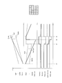
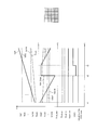
- FIG. 6 is a diagram showing an example of a timing chart when the flicker detection circuit 5 detects flicker.
- FIG. 7 is a diagram showing an example of a timing chart when the flicker detection circuit 5 does not detect flicker. The timing chart is shown on the left side in FIGS. 6 and 7, and the pixel block PB in this example is schematically shown on the right side in FIGS. 6 and 7.
- the pixel block PB is composed of 16 pixels P1 to P16 arranged in 4 rows and 4 columns.
- 16 pixels P are subscripted from left to right and from top to bottom in FIGS. 6 and 7.
- the codes “P1”, “P4”, “P13”, and “P16” are added to the pixels P arranged at the corners of the pixel block PB for easy understanding.
- the flicker detection circuit 5 is provided in the pixels P6 constituting the pixel block PB. Therefore, the pixel P6 is a pixel that does not contribute to imaging.
- the pixel P1 is the pixel P shown in the upper part of FIG. 5
- the pixel P16 is the pixel P shown in the lower part of FIG.
- Vsf1 shown in FIGS. 6 and 7 indicates the voltage of the connection node sf1 (see FIG. 5) between one electrode of the individual capacitor C421 of the pixel P1 and one electrode of the addition capacitor C61 of the addition unit 6.
- Vsum shown in FIGS. 6 and 7 indicates the voltage of the connection node of the other electrode of the addition capacitors C61 to C65 and C67 to C616 of the addition unit 6.
- Vint1 shown in FIGS. 6 and 7 indicates the output voltage of the individual subtractor 42 of the pixel P1.
- Vint 16 shown in FIGS. 6 and 7 indicates the output voltage of the individual subtractor 42 of the pixel P16.
- Vint_sum shown in FIGS. 6 and 7 indicates the output voltage of the shared subtractor 51 of the flicker detection circuit 5 provided in the pixel P6.
- Vsum_p shown in FIGS. 6 and 7 is the voltage of the connection node sum_p (see FIG. 5) which is the connection between the P-type transistor 521 and the N-type transistor 522 constituting the shared determination unit 52 of the flicker detection circuit 5. Is shown. That is, “Vsum_p” indicates the voltage of the detection signal (+) output by the shared determination unit 52.
- “Vsum_n” shown in FIGS. 6 and 7 is the voltage of the connection node sum_n (see FIG. 5) which is the connection between the P-type transistor 523 and the N-type transistor 524 constituting the shared determination unit 52 of the flicker detection circuit 5. Is shown. That is, “Vsum_n” indicates the voltage of the detection signal ( ⁇ ) output by the shared determination unit 52.
- Vsum_rst shown in FIGS. 6 and 7 indicates the voltage of the output reset signal output by the region reset generation circuit 53 provided in the flicker detection circuit 5.
- XAZ1-5, 7-16 shown in FIGS. 6 and 7 indicate a voltage applied to the gate of the P-type transistor 421 provided in each of the pixels P1 to P5 and P7 to P16.
- XAZ_sum shown in FIGS. 6 and 7 indicates a voltage applied to the gate of the P-type transistor 511 provided in the address event detection unit 4.
- FIGS. 6 and 7 The horizontal axis in FIGS. 6 and 7 represents time, and the vertical axis in FIGS. 6 and 7 represents voltage. In FIGS. 6 and 7, the passage of time is shown from left to right.
- the voltage Vsum of the connection node sum is the sum of the voltages Vsf1 to Vsf5 and Vsf7 to Vsf16 of the connection nodes sf1 to sf5 and sf7 to sf16. Therefore, the voltage Vsum has a higher rate of increase than the voltages Vsf1 to Vsf5 and Vsf7 to Vsf16.
- the output voltage Vint1 of the individual subtractor 42 provided in the pixel P1 decreases as the voltage Vsf1 rises. Further, the output voltage Vint16 of the individual subtractor 42 provided in the pixel P16 decreases as the voltage Vsf16 increases. The output voltage Vint1 of the individual subtractor 42 provided in the pixel P16 decreases as the voltage Vsf1 increases. Although not shown, the output voltages Vint2 to Vint5 and Vint7 to Vint15 of the individual subtractors 42 provided in the pixels P2 to P5 and P7 to P15 also decrease as the voltages Vsf2 to Vsf5 and Vsf7 to Vsf15 increase.
- the output voltage Vint_sum of the shared subtractor 51 also begins to decrease.
- the voltage Vint_sum has a higher reduction rate than the voltages Vint1 to Vint5 and Vint7 to Vint16.
- the region reset generation circuit 53 switches the voltage level of the output reset signal Vsum_rst from a high level to a low level based on the fact that the voltage level of the voltage Vsum_n of the detection signal (-) is switched to a high level.
- control signals XAZ1 to 5,7-16 having a low voltage level are input to the gates of the P-type transistors 421 provided in the pixels P1 to P5 and P7-P16, and the P-type transistors 421 Turns on.
- a voltage Vbdiff having a high voltage level is applied to the gates of the respective N-type transistors 423 provided in the pixels P1 to P5 and P7-P16. , The N-type transistor 423 is turned on.
- the potentials of the output voltages Vsf1 to Vsf5 and Vsf7-Vsf16 of the current-voltage conversion unit 41 at time t2 and the potentials of the ground terminals (for example, A voltage based on the potential difference from 0V) is applied.
- the output voltage Vint of the individual subtractor 42 rises based on the voltage applied to the individual capacitor C421.
- the solid-state image sensor 200 can prevent the address event detection unit 4 from detecting an address event caused by the flicker phenomenon even if the photoelectric conversion element 333 detects a change in light due to the flicker phenomenon. ..
- a control signal XAZ_sum having a low voltage level is input to the gate of the P-type transistor 511 provided in the shared subtractor 51, and the P-type transistor 511 is turned on.
- a voltage Vbdiff having a high voltage level is applied to the gate of the N-type transistor 513 provided in the shared subtractor 51, and the N-type transistor 513 is turned on. It becomes a state.
- a voltage based on the potential difference between the potential of the voltage Vsum of the connection node sum of the adder 6 and the potential of the ground terminal (for example, 0V) at the time t3 is applied to the capacitor C511 provided in the shared subtractor 51. ..
- the output voltage Vint_sum of the shared subtractor 51 rises based on the voltage applied to the capacitor C511.
- the voltage level of the output reset signal Vsum_rst switches from low level to high level, and the voltage level of the voltage Vbdiff applied to the gate of the N-type transistor 423 changes from high level to low level. Switch. As a result, the address event detection unit 4 is in a state where event detection is possible. Further, at time t4, the voltage level of the control signal XAZ_sum switches from a low level to a high level, and the voltage level of the voltage Vbdiff applied to the gate of the N-type transistor 513 switches from a low level to a high level. As a result, the flicker detection circuit 5 is in a state where flicker detection is possible.
- the photoelectric conversion element 333 provided in the pixel P1 detects a change in light due to the movement of a predetermined object, and the other pixels P2 to P5 and P7 to P16 It is assumed that the change in light is not detected. As a result, the output voltage of the current-voltage conversion unit 41 provided in the pixel P1 starts to rise, so that the voltage Vsf1 of the connection node sf1 starts to rise.
- the voltage Vsum of the connection node sum in the addition unit 6 starts to increase because the voltage Vsf1 of the connection node sf1 rises.
- the voltage value of the voltage applied to the adder capacitor C61 of the adder unit 6 connected to the individual capacitor C421 of the pixel P is smaller than the voltage Vsf1 of the connection node sf1. Therefore, the rate of increase of the voltage Vsum of the connection node sum in the addition unit 6 is lower than the rate of increase of the voltage Vsf1 of the connection node sf1.
- the output voltage of the current-voltage conversion unit 41 provided in the pixel P1 (that is, the voltage Vsf1 of the connection node sf1) is applied to the gate of the N-type transistor 434 of the quantizer 43. It is assumed that the lower limit voltage Vlow has been exceeded (below). From this, at time t2, the control signal XAZ1 having a low voltage level is applied to the gate of the P-type transistor 421 of the individual subtractor 42 provided in the pixel P1. Further, at time t2, the voltage level of the voltage Vbdiff applied to the gate of the N-type transistor 423 of the individual subtractor 42 provided in the pixel P1 is switched from a low level to a high level.
- the region reset generation circuit 53 maintains the output of the output reset signal Vsum_rst having a high voltage level.
- both the P-type transistor 421 and the N-type transistor 423 are turned on.
- a voltage based on the potential difference between the potential of the output voltage Vsf1 of the current-voltage conversion unit 41 and the potential of the ground terminal (for example, 0V) at time t2 is applied to the individual capacitor C421 provided in the pixel P1.
- the output voltage Vint of the individual subtractor 42 rises based on the voltage applied to the individual capacitor C421.
- the flicker detection circuit 5 continues the standby operation for flicker detection.
- the flicker detection circuit 5 treats the change in light as a flicker phenomenon.
- the standby operation for flicker detection can be continued without making a judgment.
- the solid-state image sensor 200 detects the change in light as an address event caused by the flicker phenomenon. It can be prevented from being stored.
- the address event detection unit 4 provided in the pixel P1 is input from the output voltage of the current-voltage conversion unit 41 at time t2 (an example of one voltage) at a timing different from that at time t2.
- the output voltage of 41 (an example of the other voltage) can be subtracted.
- the solid-state image sensor 200 in the present embodiment is quantized by turning on the P-type transistor 421 of the individual subtractor 42 provided in the address event detection unit 4 when the flicker detection circuit 5 detects the flicker.
- the detection signal (+) and the detection signal ( ⁇ ) of the device 43 are configured to be fixed at a constant voltage.
- the solid-state image sensor 200 is not limited to this configuration, and may have other configurations as long as the detection signal (+) and the detection signal ( ⁇ ) of the quantizer 43 can be fixed to a constant voltage.
- the solid-state image sensor 200 is configured to separate the pixel P that has detected the flicker phenomenon from the other pixel P.
- the solid-state image sensor 200 may have a switch between the cathode of the photoelectric conversion element 333 and the gate of the N-type transistor 413 of the logarithmic conversion circuit 41a.
- the solid-state image sensor 200 can disconnect the photoelectric conversion element 333 from the current-voltage conversion unit 41 by turning off the switch.
- the address event detection unit 4 cannot detect the address event based on the flicker phenomenon.
- the solid-state image sensor 200 can eliminate the influence of the flicker phenomenon to the maximum extent.
- the solid-state image sensor 200 according to the other configuration example 2 is at least one between the drain of the N-type transistor 411 of the logarithmic conversion circuit 41a and the power supply terminal, and between the source of the N-type transistor 411 and the cathode of the photoelectric conversion element 333. May have a switch. As a result, the supply of power to the photoelectric conversion element 333 can be cut off. As a result, the solid-state image sensor 200 can reduce that the pixel P detecting the flicker phenomenon affects the normal pixel P not detecting the flicker phenomenon. In the case of the other configuration example 2, it is not necessary to provide a switch between the cathode of the photoelectric conversion element 333 and the gate of the N-type transistor 413 as in the other configuration example 1.
- the solid-state image sensor 200 according to the other configuration example 3 has a configuration in which the output of the current-voltage conversion unit 41 is cut off.
- the solid-state image sensor 200 according to the other configuration example 3 has, for example, a switch between the connection portion (output portion of the current-voltage conversion unit 41) of the P-type transistor 414 and the N-type transistor 413 and one electrode of the individual capacitor C421. You may be doing it.
- the solid-state image sensor 200 according to the other configuration example 3 may have a switch between the drain of the P-type transistor 414 and the drain of the N-type transistor 413.
- the solid-state image sensor 200 according to the other configuration example 3 may have both of these switches. In another configuration example 3, these switches can be formed on the detection chip 202 (see FIG. 2) instead of the light receiving chip 201. Therefore, the solid-state image sensor 200 according to the other configuration example 3 can improve the degree of freedom in design.
- the solid-state image sensor 200 according to the other configuration example 4 has a configuration in which the individual subtractor 42 is blocked.
- the solid-state imaging device 200 according to the other configuration example 4 may have, for example, a switch between the other electrode of the individual capacitor C421 and the source of the P-type transistor 421.
- the switch can be formed not on the light receiving chip 201 but on the detection chip 202 as in the other configuration example 3. Therefore, the solid-state image sensor 200 according to the other configuration example 4 can improve the degree of freedom in design.
- the solid-state image sensor 200 according to the other configuration example 5 is formed between the connection portion and the transfer portion of the P-type transistor 431 and the N-type transistor 432 of the quantizer 43, and the P-type transistor 433 and the N-type of the quantizer 43.
- a switch may be provided between the connection portion and the transfer portion of the transistor 434.
- the solid-state image sensor 200 according to the other configuration example 6 has a configuration in which the pixel P is short-circuited.
- the solid-state imaging device 200 according to the other configuration example 6 may have, for example, a switch between the cathode and the ground terminal of the photoelectric conversion element 333.
- the cathode and anode of the photoelectric conversion element 333 have the same potential, and even if the photoelectric conversion element 333 receives light, the current is not output to the current-voltage conversion unit 41.
- the solid-state image sensor 200 according to the other configuration example 6 can eliminate the influence of the pixel P detecting the flicker phenomenon on the normal pixel P to the maximum extent.
- the solid-state image sensor 200 according to the other configuration example 7 has a configuration in which the voltage value of the output voltage of the current-voltage conversion unit 41 is set to a constant value.
- the solid-state image sensor 200 according to the other configuration example 7 may have, for example, a switch between the output terminal and the ground terminal of the logarithmic conversion circuit 41a.
- the logarithmic value of the output voltage of the logarithmic conversion circuit 41a becomes 0.
- the solid-state image sensor 200 according to the other configuration example 7 can minimize the influence on the normal operation of the pixel P.
- the solid-state image sensor 200 according to the other configuration example 8 may have a switch between the output terminal (output terminal of the buffer circuit 41b) of the current-voltage conversion unit 41 and the ground terminal.
- the voltage input to the individual subtractor 42 is fixed to, for example, 0V, so that the detection signal (+) and the detection signal ( ⁇ ) of the quantizer 43 also become constant values. Therefore, the solid-state image sensor 200 can prevent the address event detection unit 4 from detecting the address event even if the photoelectric conversion element 333 detects the light based on the flicker phenomenon.
- the switch can be formed not on the light receiving chip 201 but on the detection chip 202 as in the other configuration example 3. Therefore, the solid-state image sensor 200 according to the other configuration example 8 can improve the degree of freedom in design.
- the solid-state image sensor 200 according to the other configuration example 9 is configured so that the P-type transistor 421 provided in the individual subtractor 42 can be kept off.
- the solid-state image sensor 200 according to the other configuration example 9 can minimize the influence on the normal operation of the pixel P by the digital control of switching the P-type transistor 421 on and off.
- the current fluctuation of the individual subtractor 42 can be suppressed. Therefore, the solid-state image sensor 200 according to the other configuration example 9 can suppress power supply noise caused by the pixel P that has detected the flicker phenomenon.
- the solid-state image sensor 200 according to the other configuration example 10 includes the connection between the P-type transistor 431 and the N-type transistor 432 of the quantizer 43 and the power supply terminal, and the P-type transistor 433 and N-type of the quantizer 43.
- a switch may be provided between the connection portion of the transistor 434 and the ground terminal.
- the detection signal (+) output by the quantizer 43 is a signal having a high voltage level
- the detection signal ( ⁇ ) output by the quantizer 43 is a signal having a low voltage level.
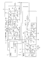
- FIG. 8 is a circuit diagram showing a configuration example of an address event detection unit 4 and a flicker detection circuit 5 provided in the solid-state image sensor 200 according to the present embodiment.
- the pixel signal generation unit 320, the transfer transistor 331, and the OFG transistor 332 provided in the pixel P are not shown.
- FIG. 9 is a circuit diagram showing a configuration example of stop circuits 45a and 45b for stopping the quantizer 43 when the flicker detection circuit 5 detects flicker.
- the address event detection unit 4 provided in the solid-state image sensor 200 has stop circuits 45a and 45b connected to the shared determination unit 52 provided in the flicker detection circuit 5. ing.
- the stop circuit 45a is connected to the connection portion of the P-type transistor 521 and the N-type transistor 522 of the shared determination unit 52.
- the stop circuit 45b is connected to the connection portion of the P-type transistor 523 and the N-type transistor 524 of the shared determination unit 52.
- the stop circuit 45a is configured to operate based on the detection signal (+) input from the shared determination unit 52.
- the stop circuit 45b is configured to operate based on the detection signal ( ⁇ ) input from the shared determination unit 52.
- the stop circuit 45a is provided between the P-type transistor 431 and the N-type transistor 432 provided in the quantizer 43.
- the stop circuit 45a has a P-type transistor 451a and an N-type transistor 452a.
- the gate of the P-type transistor 451a and the gate of the N-type transistor 452a are connected.
- the gate of the P-type transistor 451a and the gate of the N-type transistor 452a are connected to the connection portion of the P-type transistor 521 and the N-type transistor 522 of the shared determination unit 52.
- the detection signal (+) input from the shared determination unit 52 is applied to the gate of the P-type transistor 451a and the gate of the N-type transistor 452a.
- the source of the P-type transistor 451a is connected to the power supply terminal.
- the drain of the P-type transistor 451a is connected to the drain of the N-type transistor 432 provided in the quantizer 43.
- the N-type transistor 452a is arranged between the P-type transistor 431 and the N-type transistor 432.
- the P-type transistor 431, the N-type transistor 452a, and the N-type transistor 432 are connected in series between the power supply terminal and the ground terminal.
- the stop circuit 45b is provided between the P-type transistor 433 and the N-type transistor 434 provided in the quantizer 43.
- the stop circuit 45b has an N-type transistor 451b and a P-type transistor 452b.
- the gate of the N-type transistor 451b and the gate of the P-type transistor 452b are connected.
- the gate of the N-type transistor 451b and the gate of the P-type transistor 452b are connected to the connection portion of the P-type transistor 523 and the N-type transistor 524 of the shared determination unit 52.
- the detection signal ( ⁇ ) input from the shared determination unit 52 is applied to the gate of the N-type transistor 451b and the gate of the P-type transistor 452b.
- the source of the N-type transistor 451b is connected to the ground terminal.
- the drain of the N-type transistor 451b is connected to the drain of the N-type transistor 432 provided in the quantizer 43.
- the P-type transistor 452b is arranged between the P-type transistor 433 and the N-type transistor 434.
- the P-type transistor 433, the P-type transistor 452b, and the N-type transistor 434 are connected in series between the power supply terminal and the ground terminal.
- the operation of the stop circuits 45a and 45b will be described.
- the flicker detection circuit 5 does not detect flicker
- the voltage level of the detection signal (+) output from the quantizer 43 becomes a high level. Therefore, the P-type transistor 451a provided in the stop circuit 45a is turned off.
- the N-type transistor 452a provided in the stop circuit 45a is turned on. Therefore, the P-type transistor 431 and the N-type transistor 432 provided in the quantizer 43 are connected via the N-type transistor 452a.
- the flicker detection circuit 5 does not detect flicker, the voltage level of the detection signal (-) output from the quantizer 43 becomes low. Therefore, the N-type transistor 451b provided in the stop circuit 45a is turned off. On the other hand, the P-type transistor 452b provided in the stop circuit 45b is turned on. Therefore, the P-type transistor 433 and the N-type transistor 434 provided in the quantizer 43 are connected via the P-type transistor 452b.
- the quantizer 43 has a circuit configuration equivalent to not having the stop circuits 45a and 45b, and is therefore based on the voltage input from the individual subtractor 42.
- the detection signal (+) and the detection signal (-) can be output.
- the flicker detection circuit 5 detects the flicker and the output voltage of the shared determination unit 52 is higher than the upper limit threshold value Vhigh, the voltage level of the detection signal (+) output from the quantizer 43 is low. Become. Therefore, the P-type transistor 451a provided in the stop circuit 45a is turned on. On the other hand, the N-type transistor 452a provided in the stop circuit 45a is turned off. Therefore, the P-type transistor 431 and the N-type transistor 432 provided in the quantizer 43 are cut (opened) by the N-type transistor 452a. Further, the drain of the N-type transistor 432 corresponding to the output terminal of the quantizer 43 is connected to the power supply terminal via the P-type transistor 451a. As a result, the voltage of the detection signal (+) output by the quantizer 43 is fixed at a high level.
- the flicker detection circuit 5 detects flicker and the output voltage of the shared determination unit 52 is lower than the lower limit threshold value Vlow, the voltage level of the detection signal ( ⁇ ) output from the quantizer 43 becomes a high level. Therefore, the N-type transistor 451b provided in the stop circuit 45b is turned on. On the other hand, the P-type transistor 452b provided in the stop circuit 45b is turned off. Therefore, the P-type transistor 433 and the N-type transistor 434 provided in the quantizer 43 are cut (opened) by the P-type transistor 452b. Further, the drain of the N-type transistor 434 corresponding to the output terminal of the quantizer 43 is connected to the ground terminal via the N-type transistor 451b. As a result, the voltage of the detection signal ( ⁇ ) output by the quantizer 43 is fixed at a low level.
- the quantizer 43 is in a stopped state when the P-type transistors 431 and 433 and the N-type transistors 432 and 434 are disconnected (opened).
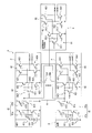
- FIG. 10 is a circuit diagram showing a configuration example of an address event detection unit 4 and a flicker detection circuit 5 provided in the solid-state image sensor 200 according to the present embodiment.
- the pixel signal generation unit 320, the transfer transistor 331, and the OFG transistor 332 provided in the pixel P are not shown.
- the solid-state image sensor 200 has a switch circuit 54a connected between the output terminal of the quantizer 43 provided in the address event detection unit 4 and the transfer unit (not shown). , 54b.
- the switch circuit 54a is arranged between the output terminal from which the detection signal (+) of the quantizer 43 is output and the transfer unit.
- the switch circuit 54b is arranged between the output terminal from which the detection signal ( ⁇ ) of the quantizer 43 is output and the transfer unit.
- the control signal input terminals of the switch circuits 54a and 54b are connected to the output terminals of the shared determination unit 52 provided in the flicker detection circuit 5. More specifically, the control signal input terminal of the switch circuit 54a is connected to the connection portion of the P-type transistor 521 and the N-type transistor 522 provided in the shared determination unit 52. The control signal input terminal of the switch circuit 54b is connected to the connection portion of the P-type transistor 523 and the N-type transistor 524 provided in the shared determination unit 52.
- the switch circuit 54a is closed (on state) when a control signal with a high voltage level is input to the control signal input terminal, and opens when a control signal with a low voltage level is input to the control signal input terminal. It becomes a state (off state).
- the switch circuit 54b is closed (on state) when a control signal with a low voltage level is input to the control signal input terminal, and opens when a control signal with a high voltage level is input to the control signal input terminal. It becomes a state (off state).
- the flicker detection circuit 5 When the flicker detection circuit 5 does not detect flicker, the voltage level of the detection signal (+) output from the quantizer 43 becomes high, and the detection signal (-) output from the quantizer 43 becomes high. The voltage level will be low. Therefore, the switch circuits 54a and 54b are in the closed state (on state). As a result, when the flicker detection circuit 5 does not detect flicker, the detection signal (+) and the detection signal ( ⁇ ) output from the quantizer 43 are input to the transfer unit.
- the flicker detection circuit 5 detects the flicker and the output voltage of the shared determination unit 52 is higher than the upper limit threshold value Vhigh, the voltage level of the detection signal (+) output from the quantizer 43 is low. Become. Therefore, the switch circuit 54a is in the open state (off state). As a result, when the flicker detection circuit 5 detects the flicker and the output voltage of the shared determination unit 52 is higher than the upper limit threshold value Vhigh, the detection signal (+) output from the quantizer 43 is not input to the transfer unit. ..
- the flicker detection circuit 5 detects flicker and the output voltage of the shared determination unit 52 is lower than the upper limit threshold value Vlow, the voltage level of the detection signal ( ⁇ ) output from the quantizer 43 becomes a high level. Therefore, the switch circuit 54a is in the open state (off state). As a result, when the flicker detection circuit 5 detects the flicker and the output voltage of the shared determination unit 52 is lower than the upper limit threshold value Vlow, the detection signal (-) output from the quantizer 43 is not input to the transfer unit. ..
- the solid-state image sensor 200 can block the output voltage of the address event detection unit 4 from being input to the transfer unit when the flicker detection circuit 5 detects the flicker. As a result, the solid-state image sensor 200 can prevent the detection of the address event based on the flicker phenomenon.
- the solid-state image sensor 200 according to the present embodiment is characterized in that it has a configuration in which capacitors corresponding to the addition capacitors of the addition unit are dispersed in each pixel.
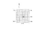
- FIG. 11 is a diagram schematically showing a pixel block PB provided in the solid-state image sensor 200 according to the present embodiment.
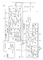
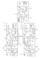
- FIG. 12 is a circuit diagram showing a configuration example of an address event detection unit 4 and a flicker detection circuit 5 provided in the solid-state image sensor 200 according to the present embodiment.
- the pixel signal generation unit 320, the transfer transistor 331, and the OFG transistor 332 provided in the pixel P are not shown.
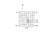
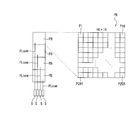
- the pixel block PB is composed of 64 pixels P1 to P64 arranged in 8 rows and 8 columns, for example.
- 64 pixels P are subscripted from left to right and from top to bottom in FIG.
- the reference numerals “P1”, “P4”, “P57” and “P64” are attached to the pixels P arranged at the corners of the pixel block PB.
- the flicker detection circuit 5 is provided in the pixels P37 constituting the pixel block PB. Therefore, the pixel P37 is a pixel that does not contribute to imaging and detection of address events.
- the pixel P not provided with the flicker detection circuit 5 (hereinafter, may be referred to as “normal pixel”) has the small capacitor C45 and the small capacitor C45 with respect to the pixel P in the first embodiment. It differs in that it has an intra-pixel reset circuit 46.
- the address event detection unit 4 provided in the pixel P64 corresponding to the normal pixel has a current-voltage conversion unit 41 having the same configuration as the current-voltage conversion unit 41 in the above 1-1 embodiment. ing. Further, the address event detection unit 4 provided in the pixel P64 has an individual subtractor 42 having the same configuration as the individual subtractor 42 in the above 1-1 embodiment. Further, the address event detection unit 4 provided in the pixel P64 has a quantizer 43 having the same configuration as the quantizer 43 in the first embodiment.
- the address event detection unit 4 provided on the pixel P64 has one electrode connected to one electrode of the individual capacitor C421 and the other electrode arranged to face the one electrode, and has an individual capacitor C421. It has a small capacitor C45 having a smaller capacitance than that of the capacitor C45.
- the small capacitor C45 has a function similar to that of the adder capacitor provided in the adder 6 in the first embodiment.
- the solid-state image sensor 200 includes an intra-pixel reset circuit 46 provided in the pixel P64.
- the intra-pixel reset circuit 46 is composed of, for example, an OR gate.
- the intra-pixel reset circuit 46 uses a voltage level control signal obtained by ORing the output reset signal RST_FL and the arbiter reset signal RST_AR of the region reset generation circuit 55 (details will be described later) provided in the flicker detection circuit 5. It is configured to output to the gate of the type transistor 421.
- the arbiter reset signal RST_AR is a reset signal output by the arbiter 213 (see FIG. 3).
- the intra-pixel reset circuit 46 When the address event detection unit 4 executes a normal operation, the intra-pixel reset circuit 46 outputs a control signal depending on the arbiter reset signal RST_AR to the gate of the P-type transistor 421. On the other hand, when the flicker detection circuit 5 detects flicker, the intra-pixel reset circuit 46 outputs a control signal depending on the output reset signal RST_FL output from the region reset generation circuit 55 to the gate of the P-type transistor 421. .. As a result, the P-type transistor 421 is controlled by the arbiter 213 when the flicker is not detected by the flicker detection circuit 5, and is controlled by the flicker detection circuit 5 when the flicker is detected by the flicker detection circuit 5. It will be.
- the pixels P1 to P36 and P38 to P65 constituting the pixel block PB have the same configuration as the pixels P64 and exhibit the same functions. Therefore, the pixels P1 to P36 and P38 to P64 correspond to an example of a plurality of individual pixels each having a photoelectric conversion element 333, a current-voltage conversion unit 41, and an individual subtractor 42.
- the pixel (hereinafter, may be referred to as “flicker monitoring pixel”) P37 provided with the flicker detection circuit 5 has substantially the same configuration as the pixels P1 to P36 and P38 to P65 of the normal pixel.
- the pixel P37 corresponds to an example of a shared pixel having a shared subtractor (an example of a shared subtractor) 51 provided in the flicker detection circuit 5.
- the pixel block PB corresponds to an example of a pixel block having a shared pixel and a plurality of individual pixels.
- the pixel P37 which is a flicker monitoring pixel, is provided with a photoelectric conversion element 333 that photoelectrically converts incident light to generate a current. Further, the pixel P37 is provided with a current-voltage conversion unit 56 that is connected to the photoelectric conversion element 333 and converts the current input from the photoelectric conversion element 333 into a voltage.
- the current-voltage conversion unit 56 has a logarithmic conversion circuit 56a and a buffer circuit 56b.
- the current-voltage conversion unit 56 is configured to convert the current (photocurrent) input from the photoelectric conversion element 333 in the logarithmic conversion circuit 56a into a voltage value of logarithmic output.
- the buffer circuit 56b has a source follower type configuration and is configured to perform impedance conversion.
- the logarithmic conversion circuit 56a constituting the current-voltage conversion unit 56 includes an N-type transistor 561, an N-type transistor 563, a P-type transistor 562, and a capacitor C56.
- these transistors for example, MOS transistors are used.
- the source of the N-type transistor 561 is connected to the cathode of the photoelectric conversion element 333.
- the drain of the N-type transistor 561 is connected to a power supply terminal (not shown).
- the P-type transistor 562 and the N-type transistor 563 are connected in series between the power supply terminal and the ground terminal. Further, the connection points of the P-type transistor 562 and the N-type transistor 563 are connected to the gate of the N-type transistor 561 and the input terminal of the buffer circuit 56b. Further, a predetermined bias voltage Vlog is applied to the gate of the P-type transistor 562.
- the gate of the N-type transistor 563 is connected to the cathode of the photoelectric conversion element 333 and the source of the N-type transistor 561.
- One electrode of the capacitor C56 is connected to the gate of the N-type transistor 563 and the connection point of the P-type transistor 562 and the N-type transistor 563.
- the other electrode of the capacitor C56 is connected to the cathode of the photoelectric conversion element 333 and the gate of the N-type transistor 563.
- the drains of the N-type transistors 561,563 are connected to the power supply side, and such a circuit is called a source follower.
- the two source followers connected in a loop form the photocurrent input from the light receiving unit 330 into a logarithmic voltage signal.
- the P-type transistor 562 supplies a constant current to the N-type transistor 563.
- the capacitor C56 is provided to stabilize the gate voltage of each of the N-type transistor 561 and the N-type transistor 563.
- the logarithmic conversion circuit 56a does not have to have the capacitor C56.
- the buffer circuit 56b has a P-type transistor 564 and a P-type transistor 565.
- transistors for example, MOS transistors are used.
- the P-type transistor 564 and the P-type transistor 565 are connected in series between the power supply terminal and the ground terminal.
- the gate of the P-type transistor 565 is connected to the output terminal (connection point of the P-type transistor 562 and the N-type transistor 563) of the logarithmic conversion circuit 56a.
- the connection points of the P-type transistor 564 and the P-type transistor 565 are connected to the input terminal of the shared subtractor 51. Further, a predetermined bias voltage Vbsf is applied to the gate of the P-type transistor 564.
- the pixel P37 is shared by being connected to the current-voltage conversion unit 56 and subtracting the other voltage from one voltage input from the current-voltage conversion unit 56 at different timings from the current-voltage conversion unit 56.
- a subtractor (an example of a shared subtraction unit) 51 is provided.
- the shared subtractor 51 in the present embodiment has the same configuration as the shared subtractor 51 in the above 1-1 embodiment, except that it has a dedicated capacitor C512.
- the shared subtractor 51 has a dedicated capacitor C512 having one electrode and the other electrode arranged to face the one electrode and connected to the other electrode of the small capacitor C45, and has a smaller capacitance than the individual capacitor C421. have.
- the dedicated capacitor C512 is provided in a flicker monitoring pixel (pixel P37) different from the individual pixels (pixels P1 and P45 in FIG. 14).
- the dedicated capacitor C512 is a capacitor dedicated to flicker monitoring provided in the flicker monitoring pixel (pixel P37).
- the dedicated capacitor C512 has the same capacity as, for example, the small capacitor C45.
- the dedicated capacitor C512 is connected to the small capacitor C45 by the wiring FLcom.
- the small capacitor C45 is provided in a pixel different from that of the shared subtractor 51, it functionally constitutes a part of the shared subtractor 51.
- the shared determination unit 52 provided in the pixel P37 has the same configuration as the shared determination unit 52 in the above 1-1 embodiment, and exhibits the same function. As described above, the pixel P37 is provided with the photoelectric conversion element 333, the current-voltage conversion unit 56, the shared subtractor 51, and the shared determination unit 52. However, since the capacity of the dedicated capacitor C512 is small, the pixel P37 cannot detect an address event based on the movement of an object or the like.
- the flicker detection circuit 5 provided in the pixel P37 the difference between the first voltage and the second voltage based on the subtraction result by the shared subtractor 51 exceeds the upper limit threshold value High or the lower limit threshold value Vlow (both are examples of predetermined threshold values). It has a shared determination unit 52 for determining whether or not it is present.
- the flicker detection circuit 5 provided in the pixel P37 has a plurality of flicker detection circuits 5 when the shared determination unit 52 determines that the voltage difference based on the subtraction result of the shared subtractor 51 exceeds the upper limit threshold value Vhigh (or the lower limit threshold value Vlow).
- the area reset generation circuit 55 is composed of, for example, an OR gate.
- the input terminal of the region reset generation circuit 55 is connected to the connection portion of the P-type transistor 521 and the N-type transistor 522 of the shared determination unit 52.
- the negative input terminal of the region reset generation circuit 55 is connected to the connection portion of the P-type transistor 523 and the N-type transistor 524 of the shared determination unit 52.
- the detection signal (+) output by the shared determination unit 52 is input to the input terminal of the area reset generation circuit 55.
- a detection signal ( ⁇ ) is input to the negative input terminal of the region reset generation circuit 55.
- the region reset generation circuit 55 outputs an output reset signal RST_FL having a high voltage level when the voltage level of the detection signal (+) is high or the voltage level of the detection signal (-) is low.
- the region reset generation circuit 55 outputs an output reset signal RST_FL having a low voltage level when the voltage level of the detection signal (+) is low and the voltage level of the detection signal ( ⁇ ) is high.
- the shared determination unit 52 outputs a signal having a high voltage level of the detection signal (+) and a low voltage level of the detection signal ( ⁇ ). ..
- the area reset generation circuit 55 outputs an output reset signal RST_FL having a high voltage level.
- an output reset signal RST_FL having a high voltage level is input to one input terminal of the intra-pixel reset circuit 46.
- the P-type transistors 421 provided in the pixels P1 to P36 and P38 to P64 are controlled by the arbiter 213.
- the area reset generation circuit 55 outputs an output reset signal RST_FL having a low voltage level.
- an output reset signal RST_FL having a low voltage level is input to one input terminal of the intra-pixel reset circuit 46.
- the P-type transistors 421 provided in the pixels P1 to P36 and P38 to P64 are controlled by the flicker detection circuit 5.
- the solid-state image sensor 200 according to the present embodiment has a small capacitor C45 corresponding to the adder capacitor of the adder unit 6 in the above 1-1 embodiment in the normal pixels constituting the pixel block PB. Further, a small capacitor C45 provided for each of the normal pixels constituting the pixel block PB is connected to the gate of the P-type transistor 512 of the shared subtractor 51 of the flicker detection circuit 5 by connecting the other electrodes to each other. .. As a result, the solid-state image sensor 200 according to the present embodiment has the same effect as the solid-state image sensor 200 according to the 1-1 embodiment.
- FIG. 13 is a diagram schematically showing a pixel block PB provided on the solid-state image sensor 200 according to the present embodiment.
- FIG. 14 is a circuit diagram showing a configuration example of an address event detection unit 4 and a flicker detection circuit 5 provided in the solid-state image sensor 200 according to the present embodiment.
- the pixel signal generation unit 320, the transfer transistor 331, and the OFG transistor 332 provided in the pixel P are not shown.
- the pixel block PB is composed of 64 pixels P1 to P64 arranged in 8 rows and 8 columns, for example.
- 64 pixels P are subscripted from left to right and from top to bottom in FIG.
- reference numerals “P1”, “P4”, “P57”, and “P64” are attached to the pixels P arranged at the corners of the pixel block PB for easy understanding.
- the flicker detection circuit 5 is provided in the pixels P37 constituting the pixel block PB, as in the first to fourth embodiments. Therefore, the pixel P37 is a pixel that does not contribute to imaging and detection of address events.
- the pixel P37 corresponds to an example of a shared pixel having a shared subtractor (an example of a shared subtractor) 51 provided in the flicker detection circuit 5.
- the pixel block PB corresponds to an example of a pixel block having a shared pixel and a plurality of individual pixels.
- the photoelectric conversion element 333 provided in the pixel P45 constituting the pixel block PB is connected to the photoelectric conversion element 333 provided in the pixel P37.
- the pixel P37 (an example of a shared pixel) is input from a photoelectric conversion element 333 (an example of a shared photoelectric conversion element) that photoelectrically converts incident light to generate a current and a photoelectric conversion element 333. It has a current-voltage conversion unit 56 (an example of a shared current-voltage conversion unit) that converts a current into a voltage and outputs the voltage to one electrode of the dedicated capacitor C512.
- the photoelectric conversion element 333 is connected to the photoelectric conversion element 333 provided in the pixel P45 (an example of one individual pixel) of the pixels P1 to P36 and P38 to P64 (an example of a plurality of individual pixels). More specifically, the cathode of the photoelectric conversion element 333 provided on the pixel P37 and the cathode of the photoelectric conversion element 333 provided on the pixel P45 are connected.
- the photoelectric conversion element 333 provided in the flicker monitoring pixel and the photoelectric conversion element 333 provided in the normal pixel the detection results in all the pixels P constituting the pixel block PB are acquired. be able to.
- the photoelectric conversion element 333 provided in the pixel P45 which is the normal pixel for PD merger to which the photoelectric conversion element 333 is merged, is affected by the photoelectric conversion element 333 provided in the pixel P37, and therefore is only operated by itself. Based on the current cannot be output to the current-voltage converter 41.
- FIG. 15 is a diagram schematically showing the arrangement relationship between the pixel block PB and the flicker detection circuit 5 provided in the solid-state image sensor 200 according to the present embodiment.
- FIG. 16 is a circuit diagram showing a configuration example of an address event detection unit 4 and a flicker detection circuit 5 provided in the solid-state image sensor 200 according to the present embodiment.
- the pixel signal generation unit 320, the transfer transistor 331, and the OFG transistor 332 provided in the pixel P are not shown.
- the pixel block PB is composed of 256 pixels P1 to P256 arranged in 16 rows and 16 columns, for example.
- 256 pixels P are subscripted from left to right and from top to bottom in FIG.
- the reference numerals “P1”, “P16”, “P241” and “P256” are attached to the pixels P arranged at the corners of the pixel block PB.
- the pixels P1 to P256 constituting the pixel block PB are not provided with the flicker detection circuit 5. Therefore, all the pixels P1 to P256 constituting the pixel block PB are pixels that contribute to imaging and detection of address events.
- the flicker detection circuit 5 is arranged in an area different from the pixel area in which a plurality of pixels P1 to P256 (an example of individual pixels) are arranged. That is, the shared subtractor 51 (see FIG. 16) provided in the flicker detection circuit 5 is arranged in a region different from the pixel region in which the plurality of pixels P1 to P256 are arranged.
- the pixels P1 to P256 in this embodiment have the same configuration as the pixels P1 to P36 and P38 to P64 in the first to fourth embodiments.
- the flicker detection circuit 5 has the same configuration as the flicker detection circuit 5 in the above 1-1 embodiment, except that the area reset generation circuit is different.
- the flicker detection circuit 5 in the present embodiment has the same configuration as the region reset generation circuit 55 provided in the flicker detection circuit 5 in the first to fourth embodiments.
- the flicker detection circuit 5 is arranged in an area different from the pixel area, it can be connected to the small capacitors C45 provided in the pixels P1 to P256 by the wiring FLcom.
- the solid-state image sensor 200 according to the present embodiment has the same effect as the solid-state image sensor 200 according to the first to fourth embodiments.
- FIG. 17 is a circuit diagram showing a configuration example of an address event detection unit 4 and a flicker detection circuit 5 provided in the solid-state image sensor 200 according to the present embodiment.
- the pixel signal generation unit 320, the transfer transistor 331, and the OFG transistor 332 provided in the pixel P are not shown.
- the solid-state image sensor 200 has a first shared switch in addition to the circuit configuration of the pixel (flicker monitoring pixel) provided with the flicker detection circuit 5 in the first to fourth embodiments.
- a 57a, a second shared switch 57b, and a large capacitor C57 are provided.
- the solid-state image sensor 200 includes a first shared switch 57a provided so as to be able to cut the other electrode of the plurality of small capacitors C45 and the other electrode of the dedicated capacitor C512.
- the solid-state image sensor 200 is connected in parallel to the dedicated capacitor C512 and has a larger capacitance than the dedicated capacitor C512, and is connected in series with the large capacitor C57 and connected in parallel with the dedicated capacitor C512. It is provided with a dual shared switch 57b.
- the first shared switch 57a and the second shared switch 57b are configured so that their opening and closing are controlled by the control signal Mode_ctl.
- the control signal input terminal of the first shared switch 57a is composed of positive logic terminals
- the control signal input terminal of the second shared switch 57b is composed of negative input terminals. Therefore, the opening and closing of the first shared switch 57a and the second shared switch 57b are always reversed. That is, when the first shared switch 57a is in the open state (off state), the second shared switch 57b is in the closed state (on state). On the other hand, when the first shared switch 57a is in the closed state (on state), the second shared switch 57b is in the open state (off state).
- the first shared switch 57a is turned on and the second shared switch 57b is turned off to connect a plurality of small capacitors C45 of normal pixels to the flicker detection circuit 5. And perform flicker detection. After the flicker detection is completed, the first shared switch 57a is turned off and the second shared switch 57b is turned on. As a result, the large capacitor C57 is connected to the shared subtractor 51, so that the gain of the shared subtractor 51 is improved. Therefore, even the pixel P provided with the flicker detection circuit 5 can detect the same address event as the normal pixel.
- the pixel having the flicker detection circuit 5 can exhibit the function as the flicker monitoring combined pixel.
- the solid-state image sensor 200 according to the 1-1 to 1-7 embodiments includes one flicker detection circuit for each of a plurality of pixels.
- the solid-state image sensor 200 according to each embodiment can reduce power consumption as compared with the case where a flicker detection circuit is provided for each pixel.
- the solid-state image sensor 200 resets the address event detection unit 4 (for example, the individual subtractor 42) before the address event caused by the flicker phenomenon occurs. As a result, it is possible to suppress the occurrence of an address event caused by the flicker phenomenon.
- FIG. 18 is a circuit diagram showing a configuration example of a low-resolution address event detection unit provided with the solid-state image sensor 200 according to the 2-1 embodiment.
- the pixel signal generation unit 320, the transfer transistor 331, and the OFG transistor 332 provided in the pixel P are not shown.
- the solid-state image sensor 200 according to the first embodiment described above except that the solid-state image sensor 200 according to the present embodiment does not have the region reset generation circuit 53 and the intra-pixel reset circuit 44. It has the same configuration as. Further, the solid-state image sensor 200 according to the present embodiment has a low-resolution system circuit 9 having the same configuration as the flicker detection circuit 5 except that the region reset generation circuit 53 according to the first-first embodiment is not connected. It has.
- the solid-state image sensor 200 is connected to each of a plurality of photoelectric conversion elements 333 and a plurality of photoelectric conversion elements 333, each of which photoelectrically converts incident light to generate a current, and is connected to each of the plurality of photoelectric conversion elements 333. It is provided with a plurality of current-voltage conversion units 41 that convert the current input from the above into a voltage. Further, the solid-state image sensor 200 is connected to a plurality of current-voltage conversion units 41 and has a first voltage based on one voltage input from each of the current-voltage conversion units 41 at different timings to a second voltage based on the other voltage. A shared subtractor (an example of a shared subtraction unit) 91 for subtracting the voltage is provided.
- the solid-state image sensor 200 determines whether or not the difference between the first voltage and the second voltage based on the subtraction result of the shared subtractor 91 exceeds the upper limit threshold value Vhigh or the lower limit threshold value Vlow (both are examples of predetermined threshold values).
- a shared determination unit 92 for determination is provided.
- the solid-state image sensor 200 includes an addition unit 6 that adds voltages output from each of the plurality of current-voltage conversion units 41.
- the shared subtractor 91 is configured to subtract the second voltage, which is the other additive voltage, from the first voltage, which is one additional voltage that is added by the adder 6 and input at different timings.
- the shared subtractor 91 includes a P-type transistor 911, a P-type transistor 912, an N-type transistor 913, and a capacitor C911.
- transistors for example, MOS transistors are used.
- the P-type transistor 912 and the N-type transistor 913 are connected in series between the power supply terminal and the ground terminal.
- the connection portion of the P-type transistor 912 and the N-type transistor 913 is connected to the input terminal of the shared determination unit 92.
- a predetermined bias voltage Vbdiff is applied to the gate of the N-type transistor 913.
- the source of the P-type transistor 911 is connected to the gate of the P-type transistor 912.
- the drain of the P-type transistor 911 is connected to the connection portion of the P-type transistor 912 and the N-type transistor 913.
- One electrode of the capacitor C911 is connected to the source of the P-type transistor 911 and the gate of the P-type transistor 912.
- the other electrode of the capacitor C911 is connected to the connection portion of the P-type transistor 912 and the N-type transistor 913 and the drain of the P-type transistor 911. Since the operation of the shared subtractor 91 is the same as that of the individual subtractor 42, the description thereof will be omitted.
- the shared determination unit 92 is composed of a quantizer.
- the shared determination unit 92 includes a P-type transistor 921, an N-type transistor 922, a P-type transistor 923, and an N-type transistor 924.
- transistors for example, MOS transistors are used.
- the P-type transistor 921 and the N-type transistor 922 are connected in series between the power supply terminal and the ground terminal.
- the P-type transistor 923 and the N-type transistor 924 are connected in series between the power supply terminal and the ground terminal.
- the gate of the P-type transistor 921 and the gate of the P-type transistor 923 are connected to the output terminal of the shared subtractor 91 (the connection portion of the P-type transistor 912 and the N-type transistor 913).
- An upper limit threshold value Vhigh of a voltage having a high voltage level is applied to the gate of the N-type transistor 922.
- a lower limit threshold value Vlow of a voltage having a low voltage level is applied to the gate of the N-type transistor 924.
- the connection portion of the P-type transistor 921 and the N-type transistor 922 is an output terminal of the detection signal (+).
- the connection portion of the P-type transistor 923 and the N-type transistor 924 is an output terminal of the detection signal ( ⁇ ).
- the shared determination unit 92 determines the voltage.
- a detection signal (+) whose level is almost the same as the power supply voltage and a detection signal (-) whose voltage level is almost the same as the voltage of the ground terminal are output.
- the voltage input from the shared subtractor 91 (that is, the voltage output by the shared subtractor 91) is the total voltage of the output voltages of the k individual subtractors 42 added by the adder 6.
- the output of the shared subtractor 91 does not exceed either the upper limit threshold value Vhigh or the lower limit threshold value Vlow, the output of the shared determination unit 92 becomes “0”, and the low resolution system circuit 9 is connected to the adder unit 6. It is detected that the address event has not occurred in all the pixels of the plurality of (k in this example) pixels.
- the shared determination unit 92 detects a detection signal whose voltage level is almost the same as that of the ground terminal. (+) And a detection signal (-) whose voltage level is almost the same as the voltage of the ground terminal are output. In this case, the output of the shared determination unit 92 becomes “+1”, and the low resolution system circuit 9 is in a dark state with a predetermined number of pixels among a plurality of (k in this example) pixels connected to the addition unit 6. Detects that an address event that changes from light to bright has occurred. The predetermined number differs depending on the capacitance of the addition capacitors C61 to C6k provided in the addition unit 6 and the capacitance of the individual capacitors C421.
- the shared determination unit 92 detects a detection signal whose voltage level is substantially the same as the power supply voltage. (+) And a detection signal (-) whose voltage level is almost the same as the power supply voltage are output.
- the output of the shared determination unit 92 is “-1”, and the low-resolution system circuit 9 is bright with a predetermined number of pixels among a plurality of (k in this example) pixels connected to the addition unit 6. Detects the occurrence of an address event that changes from state to dark.
- an address event is detected by one shared subtractor 51 and one shared determination unit 52 by using the added voltage obtained by adding the voltage based on the photocurrent of the photoelectric conversion element 333 in multiple pixels by the adding unit 6. It is configured to determine whether or not it has been done. Further, the solid-state image sensor 200 is configured so that the operation of the individual subtractor 42 and the quantizer 43, which are provided in the pixel P and do not contribute to the detection of the address event, can be stopped.
- the solid-state image sensor 200 switches to low-resolution address event detection when it is not necessary to detect address events at high resolution, and the individual subtractor 42 and quantizer that do not contribute to address event detection. The operation of 43 can be stopped. As a result, the solid-state image sensor 200 can reduce power consumption.
- FIG. 19 is a circuit diagram showing a configuration example of a low-resolution address event detection unit provided in the solid-state image sensor 200 according to the second-2 embodiment. Note that in FIG. 19, the pixel signal generation unit 320, the transfer transistor 331, and the OFG transistor 332 provided in the pixel P are not shown.
- the solid-state image sensor 200 includes a switch circuit 47 in addition to the configuration of the solid-state image sensor 200 according to the 2-1 embodiment. More specifically, the solid-state image sensor 200 is individually connected to a plurality of current-voltage conversion units 41, and the other voltage is subtracted from one voltage input from the connected current-voltage conversion units 41 at different timings. A subtractor (an example of an individual subtraction unit) 42 is provided. Each of the plurality of individual subtractors 42 has one electrode connected to the current-voltage conversion unit 41 to which the individual subtractor 42 is connected, and the other electrode arranged to face the one electrode. It includes an individual capacitor C421.
- the plurality of individual subtractors 42 have a switch circuit (an example of a switch) 47 that is connected to the other electrode of the individual capacitor C421 and can disconnect the individual capacitor C421 from the individual subtractor 42.
- the adder 7 is connected to a connection with the individual capacitor C421 and the switch circuit 47.
- the adder 7 does not have an adder capacitor, unlike the adder 6 in the 2-1 embodiment.
- the switch circuit 47 When the solid-state image sensor 200 operates at a low resolution, the switch circuit 47 is switched to an open state (off state). As a result, the components after the individual capacitor C421 can be separated from the current-voltage conversion unit 41.
- the input terminals of the shared subtractor 91 are connected to the other electrodes of the individual capacitors C421 provided in the plurality of pixels P, respectively. As a result, in the shared subtractor 91, a predetermined gain is obtained by the individual capacitor C421 and the capacitor C911. As a result, the solid-state image sensor 200 can detect whether or not an address event has occurred by the shared subtractor 91 and the shared determination unit 92 based on the voltages input from the plurality of current-voltage conversion units 41.
- the switch circuit 47 is opened to switch to the detection of the address event at low resolution and does not contribute to the detection of the address event.
- the operation of the individual subtractor 42 and the quantizer 43 can be stopped. As a result, the solid-state image sensor 200 can reduce power consumption.
- the solid-state image sensor 200 As described above, the solid-state image sensor 200 according to the 2-1 embodiment and the 2-2 embodiment stops the operation of the individual subtractor 42 and the quantizer 43 that do not contribute to the detection of the address event. It is possible to reduce power consumption.
- FIG. 20 is a circuit diagram showing a configuration example of a low-resolution address event detection unit provided with the solid-state image sensor 200 according to the 3-1 embodiment.
- the pixel signal generation unit 320, the transfer transistor 331, and the OFG transistor 332 provided in the pixel P are not shown.
- the solid-state image sensor 200 according to the first embodiment described above except that the solid-state image sensor 200 according to the present embodiment does not have the region reset generation circuit 53 and the intra-pixel reset circuit 44. It has the same configuration as. Further, the solid-state imaging device 200 according to the present embodiment includes a threshold value processing circuit 10 having the same configuration as the flicker detection circuit 5 except that the region reset generation circuit 53 according to the first-first embodiment is not connected. ing.
- the solid-state image sensor 200 In the solid-state image sensor 200 according to the present embodiment, one for each of a plurality of (four in this example) photoelectric conversion elements 333 and a plurality of photoelectric conversion elements 333, each of which photoelectrically converts incident light to generate an electric current. It is provided with a plurality of current-voltage conversion units 41 that are connected and convert the current input from the photoelectric conversion element 333 into a voltage. Further, the solid-state image sensor 200 is connected to a plurality of (four in this example) current-voltage conversion units 41, and the first voltage based on one voltage input from each of the current-voltage conversion units 41 at different timings is used as the other. It is provided with a shared subtractor (an example of a shared subtractor) 101 that subtracts a second voltage based on the voltage of.
- a shared subtractor an example of a shared subtractor
- the solid-state image sensor 200 determines whether or not the difference between the first voltage and the second voltage based on the subtraction result of the shared subtractor 101 exceeds the upper limit threshold value Vhigh or the lower limit threshold value Vlow (both are examples of predetermined threshold values).
- a shared determination unit 102 for determination is provided.
- the solid-state image sensor 200 includes an addition unit 6 that adds voltages output from each of the plurality of current-voltage conversion units 41.
- the shared subtractor 101 is configured to subtract the second voltage, which is the other additive voltage, from the first voltage, which is one additional voltage that is added by the adder 6 and input at different timings.
- the shared subtractor 101 includes a P-type transistor 1011 and a P-type transistor 1012, an N-type transistor 1013, and a capacitor C1011.
- transistors for example, MOS transistors are used.
- the P-type transistor 1012 and the N-type transistor 1013 are connected in series between the power supply terminal and the ground terminal.
- the connection portion of the P-type transistor 1012 and the N-type transistor 1013 is connected to the input terminal of the shared determination unit 102.
- a predetermined bias voltage Vbdiff is applied to the gate of the N-type transistor 1013.
- the source of the P-type transistor 1011 is connected to the gate of the P-type transistor 1012.
- the drain of the P-type transistor 1011 is connected to the connection portion of the P-type transistor 1012 and the N-type transistor 1013.
- One electrode of the capacitor C1011 is connected to the source of the P-type transistor 1011 and the gate of the P-type transistor 1012.
- the other electrode of the capacitor C1011 is connected to the connection portion of the P-type transistor 1012 and the N-type transistor 1013 and the drain of the P-type transistor 1011. Since the operation of the shared subtractor 101 is the same as that of the individual subtractor 42, the description thereof will be omitted.
- the shared determination unit 102 is composed of a quantizer.
- the shared determination unit 102 includes a P-type transistor 1021, an N-type transistor 1022, a P-type transistor 1023, and an N-type transistor 1024.
- transistors for example, MOS transistors are used.
- the P-type transistor 1021 and the N-type transistor 1022 are connected in series between the power supply terminal and the ground terminal.
- the P-type transistor 1023 and the N-type transistor 1024 are connected in series between the power supply terminal and the ground terminal.
- the gate of the P-type transistor 1021 and the gate of the P-type transistor 1023 are connected to the output terminal of the shared subtractor 101 (the connection portion of the P-type transistor 1012 and the N-type transistor 1013).
- An upper limit threshold value Vhigh of a voltage having a high voltage level is applied to the gate of the N-type transistor 1022.
- a lower limit threshold value Vlow of a voltage having a low voltage level is applied to the gate of the N-type transistor 1024.
- the connection between the P-type transistor 1021 and the N-type transistor 1022 is an output terminal for the detection signal (+).
- the connection portion of the P-type transistor 1023 and the N-type transistor 1024 is an output terminal of the detection signal ( ⁇ ).
- the shared determination unit 102 determines the voltage.
- a detection signal (+) whose level is almost the same as the power supply voltage and a detection signal (-) whose voltage level is almost the same as the voltage of the ground terminal are output.
- the voltage input from the shared subtractor 101 (that is, the voltage output by the shared subtractor 101) is the total voltage of the output voltages of the k individual subtractors 42 added by the adder 6.
- the output of the shared subtractor 101 does not exceed either the upper limit threshold value Vhigh or the lower limit threshold value Vlow, the output of the shared determination unit 102 becomes “0”, and the threshold value processing circuit 10 is connected to the adder unit 6. It is detected that the address event has not occurred in all the pixels of the plurality of pixels (4 in this example).
- the shared determination unit 102 detects a detection signal whose voltage level is almost the same as that of the ground terminal. (+) And a detection signal (-) whose voltage level is almost the same as the voltage of the ground terminal are output. In this case, the output of the shared determination unit 102 becomes "+1", and the threshold value processing circuit 10 is bright from the dark state with a predetermined number of pixels among a plurality of (4 in this example) pixels connected to the addition unit 6. Detects that an address event that changes state has occurred.
- the predetermined number differs depending on the capacities of the adder capacitors C61 to C64 provided in the adder 6 and the capacities of the individual capacitors C421.
- the shared determination unit 92 detects a detection signal whose voltage level is substantially the same as the power supply voltage. (+) And a detection signal (-) whose voltage level is almost the same as the power supply voltage are output. In this case, the output of the shared determination unit 92 becomes “-1”, and the threshold value processing circuit 10 starts from the bright state with a predetermined number of pixels among a plurality of (4 in this example) pixels connected to the addition unit 6. It detects that it has received light that changes to a dark state.
- a plurality of (four in this example) adder capacitors C61, C62, C63, and C64 provided in the adder 6 have different capacities from each other.
- the capacitance Cb of the addition capacitor C62 is four times the capacitance Ca
- the capacitance Cc of the addition capacitor C63 is eight times the capacitance Ca
- the capacitance Cd of the addition capacitor C64 is the capacitance Cc with respect to the capacitance Ca of the addition capacitor C61. It is assumed that it is 16 times.
- FIG. 21 is a diagram schematically showing an example of a weighting pattern of the pixel block PB provided in the solid-state image sensor 200 according to the present embodiment.
- the solid-state imaging device 200 includes a pixel block PB composed of a plurality of pixels P each having a photoelectric conversion element 333 and a current-voltage conversion unit 41 (see FIG. 20).
- the pixel block PB in this embodiment is composed of 64 pixels P arranged in 8 rows and 8 columns.
- pixels P connected to adder capacitors C61 to C64 having the same capacitance are arranged in a predetermined pattern.
- the addition capacitor C61 is connected to the pixels P arranged on the outermost circumference.
- the addition capacitor C62 is connected to the pixels P arranged on the second lap from the outside of the pixel block PB. Further, for example, the addition capacitor C63 is connected to the pixels P arranged on the third circumference from the outside of the pixel block PB. Further, for example, an adder capacitor C64 is connected to the pixels P arranged on the innermost circumference of the pixel block PB.
- the solid-state image sensor 200 can change the ease of detecting the address event in the pixel block PB.
- the solid-state image sensor 200 can give the pixel block PB a correction pattern to be applied in image processing.
- the processing load on the image pickup device including the solid-state image pickup device 200 is reduced, and the power consumption of the image pickup device including the solid-state image pickup device 200 can be reduced.
- FIG. 22 is a diagram showing a configuration example of a circuit for executing weighting addition and threshold processing provided in the solid-state image sensor 200 according to the present embodiment.
- the pixel signal generation unit 320, the transfer transistor 331, and the OFG transistor 332 provided in the pixel P are not shown.
- FIG. 23 is a diagram schematically showing a weighting pattern of the pixel block PB provided in the solid-state image sensor 200 according to the present embodiment.
- the solid-state image sensor 200 according to the present embodiment has the same configuration as the solid-state image sensor 200 according to the 3-1 embodiment, except for the configuration of the addition unit 8.
- the addition unit 8 provided in the solid-state image sensor 200 has a switch unit 81 provided so that a plurality of current-voltage conversion units 41 can be individually disconnected from the shared subtractor 51.
- the switch unit 81 has switches 811a, 811b, 811ka, and 811kb provided between one electrode of the individual capacitor C421 and one electrode of the plurality of adder capacitors C81a, C81b, C81ka, and C81kb.
- the switch unit 81 has switches 812a, 812b, 812ka, and 812 kb provided between the other electrode of the adder capacitors C81a, C81b, C81ka, and C81 kb and the shared subtractor 51.
- the switches 811a to 811 kb and 811a to 811 kb are composed of, for example, MOS transistors.
- the capacitances of the adder capacitors C81a, C81b, C81ka, and C81kb are different from each other.
- the solid-state image sensor 200 By switching the on / off states of the switches 811a to 811 kb and 811a to 811 kb, the solid-state image sensor 200 enables convolution calculation in addition to weighting addition.
- the capacitance Ca of the adder capacitor C81a is 1/4 of the capacitance Cb of the adder capacitor C81b.
- the switch unit 81 can set the following four states between the output of the current-voltage conversion unit 41 provided in the pixel P and the input terminal of the shared subtractor 51.
- the combined capacitor of the addition unit 8 has a capacitance Ca.
- the weighting pattern is the largest in the center, the second largest in the second lap surrounding the center, and the smallest in the third lap surrounding the second lap.
- the switch unit 81 By appropriately switching the switch unit 81, as shown from left to right in the upper row of FIG. 23, the weighting pattern can be moved one column at a time in the pixel block PB composed of the pixels P of 8 rows and 8 columns. it can. Further, by appropriately switching the switch unit 81, as shown from left to right in the lower row of FIG. 23, the weighting pattern is moved line by line in the pixel block PB composed of the pixels P of 8 rows and 8 columns. be able to.
- the solid-state image sensor 200 can execute the convolution operation by moving the weighting pattern one row or one column at a time.
- FIG. 24 is a diagram showing a configuration example of a circuit for executing weighting addition and threshold processing provided in the solid-state image sensor 200 according to the present embodiment.
- the pixel signal generation unit 320, the transfer transistor 331, and the OFG transistor 332 provided in the pixel P are not shown.
- the solid-state image sensor 200 according to the present embodiment has the same configuration as the solid-state image sensor 200 according to the third-2 embodiment, except for the configuration of the addition unit 8.
- the addition unit 8 provided in the solid-state image sensor 200 has a switch unit 81 provided so that a plurality of current-voltage conversion units 41 can be individually disconnected from the shared subtractor 51.
- the switch unit 81 has switches 812a, 812b, 812ka, and 812 kb provided between the other electrode of the adder capacitors C81a, C81b, C81ka, and C81 kb and the shared subtractor 51.
- the switches 811a to 811kb are composed of, for example, MOS transistors.
- the capacitances of the adder capacitors C81a, C81b, C81ka, and C81kb are different from each other.
- the solid-state image sensor 200 can perform a convolution operation in addition to the weighting addition.
- the capacitance Ca of the addition capacitor C81a is 1/4 of the capacitance Cb of the addition capacitor C81b.
- the switch unit 81 can set the following four states between the output of the current-voltage conversion unit 41 provided in the pixel P and the input terminal of the shared subtractor 51.
- the combined capacitor of the addition unit 8 has a capacitance Ca.
- the adder 8 provided in the solid-state image sensor 200 according to the present embodiment does not have a switch between the adder capacitors C81a to C81 kb and the individual capacitors C421.
- the solid-state image sensor 200 according to the present embodiment can reduce the circuit scale as compared with the solid-state image sensor 200 according to the 3-1 embodiment.
- FIG. 25 is a diagram showing a configuration example of a circuit for executing weighting addition and threshold processing provided in the solid-state image sensor 200 according to the present embodiment.
- the pixel signal generation unit 320, the transfer transistor 331, and the OFG transistor 332 provided in the pixel P are not shown.
- the solid-state image sensor 200 according to the present embodiment has the same configuration as the solid-state image sensor 200 according to the third-2 embodiment and the 3-3 embodiment, except for the configuration of the addition unit 8.
- the addition unit 8 provided in the solid-state image sensor 200 has a switch unit 81 provided so that a plurality of current-voltage conversion units 41 can be individually disconnected from the shared subtractor 51.
- the switch unit 81 has switches 811a, 811b, 811ka, and 811kb provided between one electrode of the individual capacitor C421 and one electrode of the plurality of adder capacitors C81a, C81b, C81ka, and C81kb.
- the switches 811a to 811kb are composed of, for example, MOS transistors.
- the capacitances of the adder capacitors C81a, C81b, C81ka, and C81kb are different from each other.
- the solid-state image sensor 200 can perform a convolution operation in addition to the weighting addition.
- the capacitance Ca of the addition capacitor C81a is 1/4 of the capacitance Cb of the addition capacitor C81b.
- the switch unit 81 can set the following four states between the output of the current-voltage conversion unit 41 provided in the pixel P and the input terminal of the shared subtractor 51.
- the combined capacitor of the addition unit 8 has a capacitance Ca.
- the adder 8 provided in the solid-state image sensor 200 according to the present embodiment does not have a switch between the adder capacitors C81a to C81kb and the shared subtractor 51.
- the solid-state image sensor 200 according to the present embodiment can reduce the circuit scale as compared with the solid-state image sensor 200 according to the 3-1 embodiment.
- the solid-state image sensor 200 can have the pixel block PB having a correction pattern applied in the image processing. As a result, the processing load on the image pickup device including the solid-state image pickup device 200 is reduced, and the power consumption of the image pickup device including the solid-state image pickup device 200 can be reduced.
- the solid-state imaging device 200 includes a photoelectric conversion element 333 that photoelectrically converts incident light to generate a current, and a photoelectric conversion element 333. It is provided with a current-voltage conversion unit 41 that converts the current input from the above into a voltage.
- the solid-state image sensor 200 is connected to the current-voltage conversion unit 41 and subtracts the other voltage from one voltage input from the current-voltage conversion unit 41 at different timings.
- the individual subtractor 42 and the shared subtractors 51, 91, 101 (An example of a plurality of subtraction units).
- the DVS sensor is a sensor that detects and outputs luminance change information.
- the luminance change information is detected for each pixel and output for each pixel.
- processing capabilities such as flicker suppression and multi-resolution support can be implemented for each pixel array area, it is possible to obtain the effects of reducing the amount of data, reducing power, and reducing noise.
- one of the plurality of subtraction units realizes the function of the conventional DVS subtraction unit, and the remaining subtraction unit performs information processing for each pixel array area. It can be used as a function.
- the solid-state image sensor 200 according to the embodiment of the present technology can exhibit a signal processing function for each region, which is impossible with the conventional DVS.
- the individual subtractor 42 of the individual subtractor 42 and the shared subtractors 51, 91, 101 (an example of a specific subtractor which is one of a plurality of subtractors) is connected to the current-voltage converter 41. It has an individual capacitor C421 having one electrode and the other electrode arranged to face the one electrode. 5, FIG. 8, FIG. 10, FIG. 12, FIG. 14, FIG. 16, FIGS. 17 to 18, 18, 22, 22, 24 and 25, as shown in the individual subtractor 42 and the shared subtractor 51,
- the shared subtractors 51, 91, 101 of 91, 101 (an example of at least a part of the remaining subtractors of the plurality of subtractors) are connected to one electrode of the individual capacitor C421.
- the individual subtractor 42 (an example of a specific subtraction unit which is one of a plurality of subtraction units) has one electrode connected to the current-voltage conversion unit 41 and the other electrode. It has an individual capacitor C421 with the other electrode arranged to face the electrode.
- the shared subtractor 91 (an example of at least a part of the subtraction part of the remainder of the plurality of subtraction parts) is connected to the other electrode of the individual capacitor C421.
- the solid-state image sensor 200 includes at least one of the address event detection unit 4 (an example of the first detection unit) or the flicker detection circuit 5, the low resolution system circuit 9 and the threshold value processing circuit 10 (all are examples of the second detection unit).
- the address event detection unit 4 the difference between the current-voltage conversion unit 41, the individual subtractor 42 (an example of the specific subtraction unit), and the difference between one voltage and the other voltage based on the subtraction result by the individual subtractor 42 is the upper limit threshold value Vhigh.
- a quantizer 43 an example of the first determination unit for determining whether or not the lower limit threshold voltage Vlow (both are examples of predetermined threshold values) is exceeded, and an address event corresponding to the amount of light received by the photoelectric conversion element 333.
- the flicker detection circuit 5, the low-resolution system circuit 9, and the threshold processing circuit 10 include shared subtractors 51, 91, 101 (an example of a subtraction unit among the residual subtraction units among a plurality of subtraction units). Shared determination to determine whether the difference between one voltage and the other voltage based on the subtraction results of the shared subtractors 51, 91, 101 exceeds the upper limit threshold Vhigh or the lower limit threshold Vlow (both are examples of predetermined thresholds). It has units 52, 92, and 102 (an example of a second determination unit).
- the solid-state image sensor 200 includes both an address event detection unit 4 and a flicker detection circuit 5, an address event detection unit 4 and a low-resolution system circuit 9, or an address event detection unit 4 and a threshold value processing circuit 10. There is.
- the solid-state image sensor 200 includes a pixel P having an address event detection unit 4 and a photoelectric conversion element 333.
- the present disclosure may have the following structure.
- a photoelectric conversion element that photoelectrically converts incident light to generate an electric current
- a current-voltage converter that converts the current input from the photoelectric conversion element into a voltage
- a solid-state image sensor including a plurality of subtractors connected to the current-voltage converter and subtracting the other voltage from one voltage input from the current-voltage converter at different timings.
- the specific subtraction unit which is one of the plurality of subtraction units, has one electrode connected to the current-voltage conversion unit and the other electrode arranged to face the one electrode.
- Has a capacitor The solid-state image sensor according to (1), wherein at least a part of the remaining subtraction part of the plurality of subtraction parts is connected to one of the electrodes.
- the specific subtraction unit which is one of the plurality of subtraction units, has one electrode connected to the current-voltage conversion unit and the other electrode arranged to face the one electrode.
- Has a capacitor The solid-state image sensor according to (1), wherein at least a part of the residual subtraction part of the plurality of subtraction parts is connected to the other electrode.
- a first determination unit for determining whether or not the difference between the current-voltage conversion unit, the specific subtraction unit, and the difference between the one voltage and the other voltage based on the subtraction result in the specific subtraction unit exceeds a predetermined threshold value.
- the first detection unit which has and detects an event according to the amount of light received by the photoelectric conversion element, or Whether or not the difference between the subtraction part of one of the residual subtraction parts of the plurality of subtraction parts and the one voltage and the other voltage based on the subtraction result in the one subtraction part exceeds a predetermined threshold value.
- the solid-state imaging device according to (2) or (3) above which includes at least one of a second detection unit having a second determination unit for determining.
- a shared subtraction unit that is connected to the plurality of current-voltage converters and subtracts a second voltage based on the other voltage from a first voltage based on one voltage input from each of the current-voltage converters at different timings.
- a solid-state image sensor (6) The solid-state image sensor according to (5), further comprising a shared determination unit for determining whether or not the difference between the first voltage and the second voltage based on the subtraction result in the shared subtraction unit exceeds a predetermined threshold value. (7) The addition unit for adding the voltage output from each of the plurality of current-voltage conversion units is provided.
- the shared subtraction unit is described in (6) above, wherein the shared subtraction unit subtracts the second voltage, which is the other addition voltage, from the first voltage, which is one addition voltage that is added by the addition unit and input at different timings.
- Solid-state imaging device It is provided with an individual subtraction unit connected to each of the plurality of current-voltage conversion units and subtracting the other voltage from one voltage input from the connected current-voltage conversion unit at different timings.
- the individual subtraction unit has an individual capacitor having one electrode connected to the current-voltage conversion unit to which the individual subtraction unit is connected and the other electrode arranged to face the one electrode.
- the addition unit includes one electrode connected to one electrode of the individual capacitor provided in the current-voltage conversion unit and the other electrode arranged to face the one electrode and connected to the common subtraction unit.
- An individual subtraction unit that is connected to each of the plurality of current-voltage conversion units and subtracts the other voltage from one voltage that is input from the connected current-voltage conversion unit at different timings.
- a reset that resets the operation of at least one of the plurality of photoelectric conversion elements, the plurality of current / voltage conversion units, and the plurality of individual subtraction units when the shared determination unit determines that the difference exceeds the threshold value.
- the solid-state imaging device according to any one of (6) to (8) above, which comprises a unit. (10) An individual subtraction unit connected to each of the plurality of current-voltage conversion units and subtracting the other voltage from one voltage input from the connected current-voltage conversion units at different timings.
- a plurality of individual pixels each having the photoelectric conversion element, the current-voltage conversion unit, and the individual subtraction unit, It is equipped with a dedicated capacitor provided in a pixel different from the individual pixel.
- Each of the plurality of individual subtraction units has an individual electrode connected to the current-voltage conversion unit to which the individual subtraction unit is connected and the other electrode arranged to face the one electrode.
- Each of the plurality of individual pixels has one electrode connected to one electrode of the individual capacitor and the other electrode arranged to face the one electrode, and has a larger capacitance than that of the individual capacitor.
- Has a small small capacitor The dedicated capacitor has one electrode and the other electrode arranged to face the one electrode and connected to the other electrode of the small capacitor, and has a smaller capacitance than the individual capacitor (5).
- a shared determination unit that determines whether or not the difference between the first voltage and the second voltage based on the subtraction result in the shared subtraction unit exceeds a predetermined threshold value.
- the solid-state imaging device which includes a reset unit.
- a shared pixel having the dedicated capacitor and the shared subtraction unit The solid-state imaging device according to (10) or (11), further comprising a pixel block having the shared pixel and the plurality of individual pixels.
- the shared pixel has a shared photoelectric conversion element that generates a current by photoelectrically converting incident light, and a shared photoelectric conversion element that converts the current input from the shared photoelectric conversion element into a voltage and transfers the voltage to one electrode of the dedicated capacitor.
- the solid-state imaging device has a shared current-voltage converter to output
- the solid-state imaging device wherein the shared photoelectric conversion element is connected to the photoelectric conversion element provided in one individual pixel of the plurality of individual pixels.
- the solid-state image sensor according to (10), wherein the shared subtraction unit is arranged in a region different from the pixel region in which the plurality of individual pixels are arranged.
- a first shared switch provided so as to be able to cut the other electrode of the plurality of small capacitors and the other electrode of the dedicated capacitor.
- a large capacitor connected in parallel to the shared capacitor and having a larger capacitance than the shared capacitor,
- the solid-state imaging device according to (10) or (12), further comprising a second shared switch connected in series to the large capacitor and connected in parallel to the shared capacitor.
- the solid according to (7) above further comprising an individual subtraction unit connected to each of the plurality of current-voltage conversion units and subtracting the other voltage from one voltage input from the connected current-voltage conversion unit at different timings.
- Image sensor 17.
- the addition unit has a switch unit provided so that the plurality of current-voltage conversion units can be individually disconnected from the common subtraction unit.
- the switch unit is a switch provided between one electrode of the individual capacitor and one electrode of the plurality of adder capacitors, and a switch provided between the other electrode of the adder capacitor and the shared subtraction unit.
- a pixel block composed of a plurality of pixels each having the photoelectric conversion element and the current-voltage conversion unit is provided.
Landscapes
- Engineering & Computer Science (AREA)
- Multimedia (AREA)
- Signal Processing (AREA)
- Transforming Light Signals Into Electric Signals (AREA)
Abstract
低消費電力化を図ることを目的とする。固体撮像素子は、入射光を光電変換して電流を生成する光電変換素子と、光電変換素子から入力される電流を電圧に変換する電流電圧変換部と、電流電圧変換部に接続されて異なるタイミングで電流電圧変換部から入力される一方の電圧から他方の電圧を減算する個別減算器及び共用減算器とを備えている。
Description
本開示は、非同期型の固体撮像素子に関する。
従来より、垂直同期信号などの同期信号に同期して画像データ(フレーム)を撮像する同期型の固体撮像素子が、撮像装置などにおいて用いられている。この一般的な同期型の固体撮像素子では、同期信号の周期(例えば、1/60秒)ごとにしか画像データを取得することができないため、交通やロボットなどに関する分野において、より高速な処理が要求された場合に対応することが困難になる。そこで、画素アドレスごとに、その画素の光量が閾値を超えた旨をアドレスイベントとしてリアルタイムに検出する検出回路を画素毎に設けた非同期型の固体撮像素子が提案されている(例えば、特許文献1参照。)。このように、画素毎にアドレスイベントを検出する固体撮像素子は、DVS(Dynamic Vision Sensor)と呼ばれる。
上述の非同期型の固体撮像素子(すなわち、DVS)では、同期型の固体撮像素子よりも遥かに高速にデータを生成して出力することができる。このため、例えば、交通分野において、人や障害物を画像認識する処理を高速に実行して、安全性を向上させることができる。しかしながら、しかしながら、アドレスイベントの検出回路は、同期型における画素回路よりもトランジスタなどの素子数が多く、消費電力が増大してしまうという問題がある。
本開示の目的は、低消費電力化を図ることができる固体撮像素子を提供することにある。
本開示による固体撮像素子は、入射光を光電変換して電流を生成する光電変換素子と、前記光電変換素子から入力される前記電流を電圧に変換する電流電圧変換部と、前記電流電圧変換部に接続されて異なるタイミングで前記電流電圧変換部から入力される一方の電圧から他方の電圧を減算する複数の減算部とを備える。
本開示による固体撮像素子は、各々が入射光を光電変換して電流を生成する複数の光電変換素子と、前記複数の光電変換素子のそれぞれに1つずつ接続されて前記光電変換素子から入力される前記電流を電圧に変換する複数の電流電圧変換部と、前記複数の電流電圧変換部に接続されて異なるタイミングで前記電流電圧変換部のそれぞれから入力される一方の電圧に基づく第一電圧から他方の電圧に基づく第二電圧を減算する共用減算部とを備える。
以下、本開示に係る技術を実施するための形態(以下、「実施形態」と称する)について図面を用いて詳細に説明する。本開示に係る技術は実施形態に限定されるものではない。以下の説明において、同一要素又は同一機能を有する要素には同一符号を用いることとし、重複する説明は省略する。なお、説明は以下の順序で行う。
1.本開示の撮像装置及び固体撮像素子の全般に関する説明
2.本開示の第1実施形態(フリッカ抑制)
3.本開示の第2実施形態(多解像度センサ)
4.本開示の第3実施形態(重み付け加算及び畳み込み演算)
1.本開示の撮像装置及び固体撮像素子の全般に関する説明
2.本開示の第1実施形態(フリッカ抑制)
3.本開示の第2実施形態(多解像度センサ)
4.本開示の第3実施形態(重み付け加算及び畳み込み演算)
本開示の各実施形態による固体撮像素子の共通する構成及び当該固体撮像素子が用いられる撮像装置の構成について図1から図4を用いて説明する。まず、各実施形態による固体撮像素子が用いられる撮像装置の概略構成について図1を用いて説明する。
図1は、本開示の各実施形態における撮像装置100の一構成例を示すブロック図である。
図1に示すように、撮像装置100は、撮像レンズ110、固体撮像素子200、記録部120および制御部130を備える。撮像装置100としては、産業用ロボットに搭載されるカメラや、車載カメラなどが想定される。
図1に示すように、撮像装置100は、撮像レンズ110、固体撮像素子200、記録部120および制御部130を備える。撮像装置100としては、産業用ロボットに搭載されるカメラや、車載カメラなどが想定される。
撮像レンズ110は、入射光を集光して固体撮像素子200に導くものである。固体撮像素子200は、入射光を光電変換して画像データを撮像するものである。固体撮像素子200は、撮像した画像データに対して、画像認識処理などの所定の信号処理を画像データに対して実行し、その処理結果とアドレスイベントの検出信号とを示すデータを記録部120に信号線209を介して出力する。
記録部120は、固体撮像素子200からのデータを記録するものである。制御部130は、固体撮像素子200を制御して画像データを撮像させるものである。
次に、本開示の各実施形態による固体撮像素子200について図2から図4を用いて説明する。
図2は、固体撮像素子200の積層構造の一例を示す図である。図2に示すように、固体撮像素子200は、検出チップ202と、検出チップ202に積層された受光チップ201とを備える。検出チップ202及び受光チップ201は、ビアなどの接続部を介して電気的に接続される。なお、ビアの他、Cu-Cu接合やバンプにより接続することもできる。
図2は、固体撮像素子200の積層構造の一例を示す図である。図2に示すように、固体撮像素子200は、検出チップ202と、検出チップ202に積層された受光チップ201とを備える。検出チップ202及び受光チップ201は、ビアなどの接続部を介して電気的に接続される。なお、ビアの他、Cu-Cu接合やバンプにより接続することもできる。
図3は、本開示の各実施形態による固体撮像素子200の一構成例を示すブロック図である。図3に示すように、固体撮像素子200は、駆動回路211、信号処理部212、アービタ213、カラムADC220および画素アレイ部300を備える。
画素アレイ部300には、複数の画素が二次元格子状に配列される。また、画素アレイ部300は、それぞれが所定数の画素からなる複数の画素ブロックに分割される。以下、水平方向に配列された画素または画素ブロックの集合を「行」と称し、行に垂直な方向に配列された画素または画素ブロックの集合を「列」と称する。
画素のそれぞれは、光電流に応じた電圧のアナログ信号を画素信号として生成する。また、画素のそれぞれは、光電流の変化量が所定の閾値を超えたか否かにより、アドレスイベントの有無を検出する。そして、アドレスイベントが生じた際に画素ブロックは、リクエストをアービタに出力する。画素ブロックは、実施形態ごとに異なる機能を発揮するように構成されている。画素ブロックの機能については後述する。
駆動回路211は、画素のそれぞれを駆動して画素信号をカラムADC220に出力させるものである。
アービタ213は、それぞれの画素からのリクエストを調停し、調停結果に基づいて応答を画素に送信するものである。応答を受け取った画素は、検出結果を示す検出信号を駆動回路211および信号処理部212に供給する。
カラムADC220は、画素ブロックの列ごとに、その列からのアナログの画素信号をデジタル信号に変換するものである。このカラムADC220は、デジタル信号を信号処理部212に供給する。
信号処理部212は、カラムADC220からのデジタル信号に対し、CDS(Correlated Double Sampling)処理や画像認識処理などの所定の信号処理を実行するものである。信号処理部212は、処理結果を示すデータと検出信号とを信号線209を介して記録部120に供給する。
図4は、本開示の各実施形態における画素Pの一構成例を示す回路図である。画素アレイ部300は、m行×n列(m及びnは自然数)に配列された複数の画素Pを有している。複数の画素Pは、画素アレイ部300において例えばマトリクス状に配列されている。
図4に示すように、画素Pは、画素信号生成部320と、受光部330と、アドレスイベント検出部4とを備える。画素Pの列ごとに、垂直信号線VSLが配線される。画素Pの列数をn(nは自然数)とすると、n本の垂直信号線VSLが配列される。
受光部330は、入射光を光電変換して光電流を生成するものである。受光部330は、駆動回路211の制御に従って、画素信号生成部320およびアドレスイベント検出部4のいずれかに光電流を供給する。
画素信号生成部320は、光電流に応じた電圧の信号を画素信号SIGとして生成するものである。画素信号生成部320は、生成した画素信号SIGを垂直信号線VSLを介してカラムADC220に供給する。
アドレスイベント検出部4は、受光部330からの光電流の変化量が所定の閾値を越えたか否かにより、アドレスイベントの有無を検出するものである。アドレスイベントは、例えば、光電流の変化量が上限の閾値を越えた(上回った)旨を示すオンイベントと、光電流の変化量が下限の閾値を越えた(下回った)旨を示すオフイベントとで構成される。また、アドレスイベントの検出信号は、例えば、オンイベントの検出結果を示す1ビットと、オフイベントの検出結果を示す1ビットとで構成される。なお、アドレスイベント検出部4は、オンイベントのみを検出することもできる。
アドレスイベントが発生した際に、アドレスイベント検出部4は、検出信号の送信を要求するリクエストをアービタ213に供給する。そして、リクエストに対する応答をアービタ213から受け取ると、アドレスイベント検出部4は、検出信号を駆動回路211および信号処理部212に供給する。
図4に示すように、画素信号生成部320は、リセットトランジスタ321、増幅トランジスタ322、選択トランジスタ323および浮遊拡散層324を備える。受光部330は、アドレスイベント検出部4に接続されている。
また、受光部330は、転送トランジスタ331、OFG(Over Flow Gate)トランジスタ332及び光電変換素子333を備える。転送トランジスタ331、OFGトランジスタ332及び光電変換素子333は、画素Pごとに配置される。転送トランジスタ331には、駆動回路211(図3参照)により転送信号TRGが供給される。OFGトランジスタ332には、駆動回路211により制御信号OFGが供給される。
また、リセットトランジスタ321、増幅トランジスタ322および選択トランジスタ323として、例えば、N型のMOS(Metal-Oxide-Semiconductor)トランジスタが用いられる。転送トランジスタ331およびOFGトランジスタ332についても、同様にN型のMOSトランジスタが用いられる。
また、光電変換素子333のそれぞれは、受光チップ201(図2参照)に配置される。光電変換素子333以外の素子の全ては、検出チップ202(図2参照)に配置される。
光電変換素子333は、入射光を光電変換して電荷を生成するものである。転送トランジスタ331は、転送信号TRGに従って、対応する光電変換素子333から浮遊拡散層324へ電荷を転送するものである。OFGトランジスタ332は、制御信号OFGに従って、対応する光電変換素子333により生成された電気信号をアドレスイベント検出部4に供給するものである。ここで、供給される電気信号は、電荷からなる光電流である。
浮遊拡散層324は、電荷を蓄積して蓄積した電荷の量に応じた電圧を生成するものである。リセットトランジスタ321は、駆動回路211からのリセット信号に従って浮遊拡散層324の電荷量を初期化するものである。増幅トランジスタ322は、浮遊拡散層324の電圧を増幅するものである。選択トランジスタ323は、駆動回路211からの選択信号SELに従って、増幅された電圧の信号を画素信号SIGとして垂直信号線VSLを介してカラムADC220(図3参照)へ出力するものである。
駆動回路211は、制御部130によりアドレスイベントの検出開始が指示されると、全ての画素PのOFGトランジスタ332を制御信号OFGにより駆動して光電流を供給させる。これにより、アドレスイベント検出部4には、画素Pの受光部330の光電流が供給される。
そして、ある画素Pにおいてアドレスイベントが検出されると、駆動回路211は、その画素PのOFGトランジスタ332をオフ状態にしてアドレスイベント検出部4への光電流の供給を停止させる。次いで駆動回路211は、転送信号TRGにより、それぞれの転送トランジスタ331を順に駆動して、電荷を浮遊拡散層324に転送させる。これにより、画素ブロック310内の複数の画素のそれぞれの画素信号が順に出力される。
このように、固体撮像素子200は、アドレスイベントが検出された画素Pの画素信号のみをカラムADC220に出力する。これにより、アドレスイベントの有無に関わらず、全画素の画素信号を出力する場合と比較して、固体撮像素子200の消費電力や、画像処理の処理量を低減することができる。
〔第1実施形態〕
次に、本開示の第1実施形態による固体撮像素子について図5から図17を用いて説明する。第1実施形態では、第1-1実施形態から第1-7実施形態に分けて、7種類のフリッカ抑制技術について説明する。
次に、本開示の第1実施形態による固体撮像素子について図5から図17を用いて説明する。第1実施形態では、第1-1実施形態から第1-7実施形態に分けて、7種類のフリッカ抑制技術について説明する。
ところで、屋内に設置された照明装置や表示装置などの発光装置が、一定周波数で高速に点滅させるダイナミック点灯(パルス点灯又はデューティ点灯)で駆動されている場合、これらの装置には、フリッカ(細かい明暗(ちらつき))現象が生じる場合がある。固体撮像素子は、屋内で使用された場合、このフリッカ現象に起因する明暗をアドレスイベントとして誤検出する場合がある。これにより、固体撮像素子は、アドレスイベントの検出精度が低下してしまう可能性がある。本実施形態による固体撮像素子は、フリッカ現象に起因するアドレスイベントの検出精度の劣化を抑制できる点に特徴を有している。
[第1-1実施形態]
図5は、第1-1実施形態による固体撮像素子200に設けられたアドレスイベント検出部4及びフリッカ検出回路5の一構成例を示す回路ブロック図である。なお、図5では、画素Pに設けられた画素信号生成部320、転送トランジスタ331及びOFGトランジスタ332の図示は省略されている。
図5は、第1-1実施形態による固体撮像素子200に設けられたアドレスイベント検出部4及びフリッカ検出回路5の一構成例を示す回路ブロック図である。なお、図5では、画素Pに設けられた画素信号生成部320、転送トランジスタ331及びOFGトランジスタ332の図示は省略されている。
図5に示すように、固体撮像素子200は、複数のアドレスイベント検出部4と、複数のアドレスイベント検出部4に接続された加算部6と、加算部6に接続されたフリッカ検出回路5とを備えている。加算部6及びフリッカ検出回路5に接続されるアドレスイベント検出部4の個数kは、画素アレイ部300に配列された画素Pの総数(m×n個)以下の自然数である。アドレスイベント検出部4は、画素Pごとに形成されている。このため、本実施形態による固体撮像素子200は、(m×n)/k個の加算部6及びフリッカ検出回路5を備える。
図5に示すように、固体撮像素子200に備えられた画素Pのそれぞれに設けられたアドレスイベント検出部4は、同一の構成を有している。アドレスイベント検出部4は、電流電圧変換部41、減算器(個別減算部の一例)430、量子化器(判定部の一例)43及び転送部(不図示)を有している。電流電圧変換部41は、対数変換回路41a及びバッファ回路41bを有している。
図5に示すように、固体撮像素子200は、各々が入射光を光電変換して電流を生成する複数(図5では2つ図示されている)の光電変換素子333を備えている。また、固体撮像素子200は、複数の光電変換素子333のそれぞれに1つずつ接続されて光電変換素子333から入力される電流を電圧に変換する複数(図5では2つ図示されている)の電流電圧変換部41を備えている。電流電圧変換部41は、対数変換回路41aと、バッファ回路41bとを有している。電流電圧変換部41は、対数変換回路41aにおいて光電変換素子333から入力される電流(光電流)を、対数出力の電圧値に変換するように構成されている。バッファ回路41bは、ソースフォロア型の構成を有し、インピーダンス変換を行うように構成されている。
図5に示すように、固体撮像素子200は、複数の電流電圧変換部41のそれぞれに1つずつ接続されて、接続された電流電圧変換部41から異なるタイミングで電流電圧変換部41から入力される一方の電圧から他方の電圧を減算する個別減算器(個別減算部の一例)42を備えている。個別減算器42は、駆動回路211(図3参照)からの行駆動信号がオン状態からオフ状態に切り替わったタイミングでの電圧との差分の電圧を出力するように構成されている。
量子化器43は、2つの閾値を用いて、個別減算器42から入力される電圧信号をデジタル信号に量子化して検出信号(+)及び検出信号(-)として転送部に出力するように構成されている。
転送部は、量子化器43から入力される検出信号(+)及び検出信号(-)を信号処理部212等に転送するように構成されている。転送部は、アドレスイベントが検出された際に、検出信号の送信を要求するリクエストをアービタ213に供給する。そして、転送部450は、リクエストに対する応答をアービタ213から受け取ると、検出信号(+)及び検出信号(-)を駆動回路211および信号処理部212に供給する。
次に、アドレスイベント検出部4の各構成要素の具体的な構成について説明する。
図5に示すように、電流電圧変換部41を構成する対数変換回路41aは、N型トランジスタ411、N型トランジスタ413、P型トランジスタ412及びコンデンサC41を有している。これらのトランジスタとして、例えばMOSトランジスタが用いられる。
図5に示すように、電流電圧変換部41を構成する対数変換回路41aは、N型トランジスタ411、N型トランジスタ413、P型トランジスタ412及びコンデンサC41を有している。これらのトランジスタとして、例えばMOSトランジスタが用いられる。
N型トランジスタ411のソースは、光電変換素子333のカソードに接続されている。N型トランジスタ411のドレインは、電源端子(不図示)に接続されている。P型トランジスタ412及びN型トランジスタ413は、電源端子と接地端子との間において、直列に接続されている。また、P型トランジスタ412及びN型トランジスタ413の接続点は、N型トランジスタ411のゲートとバッファ回路41bの入力端子とに接続される。また、P型トランジスタ412のゲートには、所定のバイアス電圧Vblogが印加される。
N型トランジスタ413のゲートは、光電変換素子333のカソード及びN型トランジスタ411のソースに接続されている。コンデンサC41の一方の電極は、N型トランジスタ413のゲート並びにP型トランジスタ412及びN型トランジスタ413の接続点に接続されている。コンデンサC41の他方の電極は、光電変換素子333のカソード及びN型トランジスタ413のゲートに接続されている。
N型トランジスタ411および413のドレインは電源側に接続されており、このような回路はソースフォロワと呼ばれる。これらのループ状に接続された2つのソースフォロワにより、受光部330から入力される光電流は、その対数の電圧信号に変換される。また、P型トランジスタ412は、一定の電流をN型トランジスタ413に供給する。コンデンサC41は、N型トランジスタ411及びN型トランジスタ413のそれぞれのゲート電圧を安定化するために設けられている。対数変換回路41aは、コンデンサC41を有していなくてもよい。
図5に示すように、バッファ回路41bは、P型トランジスタ414及びP型トランジスタ415を有している。これらのトランジスタとして、例えばMOSトランジスタが用いられる。P型トランジスタ414及びP型トランジスタ415は、電源端子と接地端子との間において、直列に接続されている。P型トランジスタ415のゲートは、対数変換回路41aの出力端子(P型トランジスタ412及びN型トランジスタ413の接続点)に接続されている。P型トランジスタ414及びP型トランジスタ415の接続点は、個別減算器42の入力端子に接続されている。また、P型トランジスタ414のゲートには、所定のバイアス電圧Vbsfが印加される。
図5に示すように、個別減算器42は、P型トランジスタ421、P型トランジスタ422、N型トランジスタ423及びコンデンサC422を有している。これらのトランジスタとして、例えばMOSトランジスタが用いられる。また、個別減算器42は、個別減算器42が接続された電流電圧変換部41に接続される一方の電極と、当該一方の電極に対向して配置された他方の電極とを有する個別コンデンサC421を有している。
P型トランジスタ422及びN型トランジスタ423は、電源端子と接地端子との間において、直列に接続されている。P型トランジスタ422及びN型トランジスタ423の接続部は、量子化器43の入力端子に接続されている。N型トランジスタ423のゲートには、所定のバイアス電圧Vbdiffが印加される。
P型トランジスタ421のソースは、P型トランジスタ422のゲートに接続されている。P型トランジスタ421のドレインは、P型トランジスタ422及びN型トランジスタ423の接続部に接続されている。P型トランジスタ421のゲートは、画素Pに設けられた画素内リセット回路44の出力端子に接続されている。画素内リセット回路44の詳細については後述する。
個別コンデンサC421の一方の電極は、バッファ回路41bの出力端子(P型トランジスタ414及びP型トランジスタ415の接続部)に接続されている。個別コンデンサC421の他方の電極は、P型トランジスタ421のソース及びP型トランジスタ422のゲートに接続されている。
コンデンサC422の一方の電極は、個別コンデンサC421の他方の電極、P型トランジスタ421のソース及びP型トランジスタ422のゲートに接続されている。コンデンサC422の他方の電極は、P型トランジスタ422及びN型トランジスタ423の接続部及びP型トランジスタ421のドレインに接続されている。
P型トランジスタ421がオフ状態からオン状態に切り替えられるとともに、N型トランジスタ423がオフ状態からオン状態に切り替えられる。これにより、個別コンデンサC421の一方の電極には、P型トランジスタ421及びN型トランジスタ423の状態が切り替わった時点(タイミング)において電流電圧変換部41から入力される電圧(一方の電圧の一例)が印加される。これに対し、個別コンデンサC421の他方の電極には、接地端子の電圧が印加される。このとき、個別コンデンサC421に蓄積されている電荷Qinitは、個別コンデンサC421の容量をC1とすると、次の式(1)により表される。一方、コンデンサC422の両端は、短絡されているため、その蓄積電荷はゼロとなる。
Qinit=C1×Vinit ・・・(1)
Qinit=C1×Vinit ・・・(1)
P型トランジスタ421がオフ状態からオン状態に切り替えられた後の所定時間後に、P型トランジスタ421がオン状態からオフ状態に切り替えられるとともに、N型トランジスタ423がオン状態からオフ状態に切り替えられる。これにより、個別コンデンサC421には、電流電圧変換部41から入力される電圧に応じた電圧(他方の電圧の一例)が印加される。電流電圧変換部41から入力される電圧をVafterとすると、個別コンデンサC421に蓄積される電荷Qafterは、次の式(2)により表される。
Qafter=C1×Vafter ・・・(2)
Qafter=C1×Vafter ・・・(2)
一方、コンデンサC422に蓄積される電荷Q2は、出力電圧をVdiff_afterとすると、次の式(3)により表される。
Q2=-C2×Vdiff_after ・・・(3)
Q2=-C2×Vdiff_after ・・・(3)
このとき、個別コンデンサC421及びコンデンサC422の総電荷量は変化しない(電荷保存の法則)ため、次の式(4)が成立する。
Qinit=Qafter+Q2 ・・・(4)
Qinit=Qafter+Q2 ・・・(4)
式(4)に式(1)から式(3)を代入して変形すると、次の式が得られる。
Vdiff_after=
-(C1/C2)×(Vdiff_after-Vinit) ・・・(5)
Vdiff_after=
-(C1/C2)×(Vdiff_after-Vinit) ・・・(5)
式(5)は、電圧信号の減算動作を表し、減算結果の利得はC1/C2となる。通常、利得を最大化することが望まれるため、個別コンデンサC421の容量C1を大きく、コンデンサC422の容量C2を小さく設計することが好ましい。一方、コンデンサC422の容量C2が小さすぎると、kTCノイズが増大し、ノイズ特性が悪化するおそれがある。このため、コンデンサC422の容量C2の容量削減は、ノイズを許容することができる範囲に制限される。また、画素Pごとに個別減算器42を含むアドレスイベント検出部4が搭載される。このため、個別コンデンサC421の容量C1やコンデンサC422の容量C2には、面積上の制約がある。これらを考慮して、個別コンデンサC421の容量C1及びコンデンサC422の容量C2の値が決定される。
図5に示すように、量子化器43は、P型トランジスタ431、N型トランジスタ432、P型トランジスタ433及びN型トランジスタ434を有している。これらのトランジスタとして、例えばMOSトランジスタが用いられる。
P型トランジスタ431及びN型トランジスタ432は、電源端子と接地端子との間において、直列に接続されている。P型トランジスタ433及びN型トランジスタ434は、電源端子と接地端子との間において、直列に接続されている。P型トランジスタ431のゲート及びP型トランジスタ433のゲートは、個別減算器42の出力端子(P型トランジスタ422及びN型トランジスタ423の接続部)に接続されている。N型トランジスタ432のゲートには、電圧レベルが高レベルの電圧の上限閾値Vhighが印加される。N型トランジスタ434のゲートには、電圧レベルが低レベルの電圧の下限閾値Vlowが印加される。P型トランジスタ431及びN型トランジスタ432の接続部は、検出信号(+)の出力端子であり、転送部の入力端子に接続されている。P型トランジスタ433及びN型トランジスタ434の接続部は、検出信号(-)の出力端子であり、転送部の他の入力端子に接続されている。
量子化器43は、個別減算器42から入力される電圧の電圧値が上限閾値Vhigh及び下限閾値Vlowの間にある場合(上限閾値Vhigh及び下限閾値Vlowのいずれも越えない場合)には、電圧レベルが電源電圧とほぼ同じレベルの検出信号(+)と、電圧レベルが接地端子の電圧とほぼ同じレベルの検出信号(-)とを出力する。この場合、量子化器43の出力は「0」となり、アドレスイベント検出部4は、光電変換素子333の受光量に応じたイベントが発生していないことを検出する。
量子化器43は、個別減算器42から入力される電圧の電圧値が上限閾値Vhighを越えた場合(上限閾値Vhighを上回った場合)には、電圧レベルが接地端子とほぼ同じレベルの検出信号(+)と、電圧レベルが接地端子の電圧とほぼ同じレベルの検出信号(-)とを出力する。この場合、量子化器43の出力は「+1」となり、アドレスイベント検出部4は、光電変換素子333の受光量に応じたオンイベントが発生したことを検出する。
量子化器43は、個別減算器42から入力される電圧の電圧値が下限閾値Vlowを越えた場合(下限閾値Vlowを下回った場合)には、電圧レベルが電源電圧とほぼ同じレベルの検出信号(+)と、電圧レベルが電源電圧とほぼ同じレベルの検出信号(-)とを出力する。この場合、量子化器43の出力は「-1」となり、アドレスイベント検出部4は、光電変換素子333の受光量に応じたオフイベントが発生したことを検出する。
画素内リセット回路44は、例えばORゲートで構成されている。画素内リセット回路44は、フリッカ検出回路5に設けられた領域リセット生成回路53(詳細は後述する)の出力リセット信号Vsum_rst及び行駆動信号を論理和して得られる電圧レベルの制御信号をP型トランジスタ421のゲートに出力するように構成されている。アドレスイベント検出部4が通常の動作を実行する場合には、画素内リセット回路44は、行駆動信号に依存する制御信号をP型トランジスタ421のゲートに出力する。一方、画素内リセット回路44は、フリッカ検出回路5がフリッカを検出した場合には、出力リセット信号Vsum_rstに依存する制御信号をP型トランジスタ421のゲートに出力する。これにより、画素内リセット回路44は、フリッカ検出回路5でフリッカが検出されたか否かに応じて適切な制御信号を出力することができる。
図5に示すように、固体撮像素子200に備えられたフリッカ検出回路5は、複数(本例ではk個)の電流電圧変換部41に接続されて異なるタイミングで電流電圧変換部41のそれぞれから入力される一方の電圧に基づく第一電圧から他方の電圧に基づく第二電圧を減算する共用減算器51を有している。フリッカ検出回路5は、共用減算器(共用減算部の一例)51での減算結果に基づく第一電圧及び第二電圧の差分が上限閾値Vhigh及び下限閾値Vlow(いずれも所定の閾値の一例)を越えたか否かを判定する共用判定部52を有している。フリッカ検出回路5は、共用減算器51での減算結果に基づく当該差分が上限閾値Vhigh(又は下限閾値Vlow)を越えたと共用判定部52が判定した場合に、複数の光電変換素子333、複数の電流電圧変換部41及び複数の個別減算器42の少なくともいずれか1つの動作をリセットする領域リセット生成回路(リセット部の一例)53を有している。
次に、フリッカ検出回路5の各構成要素の具体的な構成について説明する。
図5に示すように、共用減算器51は、P型トランジスタ511、P型トランジスタ512、N型トランジスタ513及びコンデンサC511を有している。これらのトランジスタとして、例えばMOSトランジスタが用いられる。
図5に示すように、共用減算器51は、P型トランジスタ511、P型トランジスタ512、N型トランジスタ513及びコンデンサC511を有している。これらのトランジスタとして、例えばMOSトランジスタが用いられる。
P型トランジスタ512及びN型トランジスタ513は、電源端子と接地端子との間において、直列に接続されている。P型トランジスタ512及びN型トランジスタ513の接続部は、共用判定部52の入力端子に接続されている。N型トランジスタ513のゲートには、所定のバイアス電圧Vbdiffが印加される。
P型トランジスタ511のソースは、P型トランジスタ512のゲートに接続されている。P型トランジスタ511のドレインは、P型トランジスタ512及びN型トランジスタ513の接続部に接続されている。P型トランジスタ512のゲートには、領域リセット生成回路53の出力信号や行駆動信号などが印加されるように構成されている。
コンデンサC511の一方の電極は、P型トランジスタ511のソース及びP型トランジスタ512のゲートに接続されている。コンデンサC511の他方の電極は、P型トランジスタ512及びN型トランジスタ513の接続部及びP型トランジスタ511のドレインに接続されている。共用減算器51の動作は、個別減算器42と同様であるため、説明は省略する。
図5に示すように、共用判定部52は、量子化器で構成されている。共用判定部52は、P型トランジスタ521、N型トランジスタ522、P型トランジスタ523及びN型トランジスタ524を有している。これらのトランジスタとして、例えばMOSトランジスタが用いられる。
P型トランジスタ521及びN型トランジスタ522は、電源端子と接地端子との間において、直列に接続されている。P型トランジスタ523及びN型トランジスタ524は、電源端子と接地端子との間において、直列に接続されている。P型トランジスタ521のゲート及びP型トランジスタ523のゲートは、共用減算器51の出力端子(P型トランジスタ512及びN型トランジスタ513の接続部)に接続されている。N型トランジスタ522のゲートには、電圧レベルが高レベルの電圧の上限閾値Vhighが印加される。N型トランジスタ524のゲートには、電圧レベルが低レベルの電圧の下限閾値Vlowが印加される。P型トランジスタ521及びN型トランジスタ522の接続部は、検出信号(+)の出力端子であり、領域リセット生成回路53の入力端子に接続されている。P型トランジスタ523及びN型トランジスタ524の接続部は、検出信号(-)の出力端子であり、領域リセット生成回路53の他の入力端子に接続されている。
共用判定部52は、共用減算器51から入力される電圧の電圧値が上限閾値Vhigh及び下限閾値Vlowの間にある場合(上限閾値Vhigh及び下限閾値Vlowのいずれも越えない場合)には、電圧レベルが電源電圧とほぼ同じレベルの検出信号(+)と、電圧レベルが接地端子の電圧とほぼ同じレベルの検出信号(-)とを出力する。詳細は後述するが、共用減算器51から入力される電圧(すなわち、共用減算器51が出力する電圧)は、加算部6で加算されたk個の個別減算器42の出力電圧の総電圧である。このため、共用減算器51の出力電圧が上限閾値Vhigh及び下限閾値Vlowのいずれも越えない場合、共用判定部52の出力は「0」となり、フリッカ検出回路5は、光電変換素子333が受光する光にフリッカ現象が生じていないことを検出する。
共用判定部52は、共用減算器51から入力される電圧の電圧値が上限閾値Vhighを越えた場合(上限閾値Vhighを上回った場合)には、電圧レベルが接地端子とほぼ同じレベルの検出信号(+)と、電圧レベルが接地端子の電圧とほぼ同じレベルの検出信号(-)とを出力する。この場合、共用判定部52の出力は「+1」となり、フリッカ検出回路5は、光電変換素子333が受光する光に暗状態から明状態に変化するフリッカ現象が生じていることを検出する。
共用判定部52は、共用減算器51から入力される電圧の電圧値が下限閾値Vlowを越えた場合(下限閾値Vlowを下回った場合)には、電圧レベルが電源電圧とほぼ同じレベルの検出信号(+)と、電圧レベルが電源電圧とほぼ同じレベルの検出信号(-)とを出力する。この場合、共用判定部52の出力は「-1」となり、フリッカ検出回路5は、光電変換素子333が受光する光に明状態から暗状態に変化するフリッカ現象が生じていることを検出する。
図5に示すように、領域リセット生成回路53は、共用判定部52が出力する検出信号(+)及び検出信号(-)が入力されるように構成されている。領域リセット生成回路53は、検出信号(+)及び検出信号(-)の電圧レベルに応じて、所定の電圧レベルの出力リセット信号Vsum_rstを出力するように構成されている。領域リセット生成回路53は例えば、電圧レベルが電源電圧とほぼ同じレベルの検出信号(+)と、電圧レベルが接地端子の電圧とほぼ同じレベルの検出信号(-)とが入力された場合には、電圧レベルが高レベルの出力リセット信号Vsum_rstを出力する。これにより、画素内リセット回路44が出力する出力信号は、行駆動信号に依存する制御信号となる。その結果、個別減算器42に設けられたP型トランジスタ421は、出力リセット信号Vsum_rstに制御されてオン状態にはならない。
一方、領域リセット生成回路53は例えば、電圧レベルが接地端子とほぼ同じレベルの検出信号(+)と、電圧レベルが接地端子の電圧とほぼ同じレベルの検出信号(-)とが入力された場合には、電圧レベルが低レベルの出力リセット信号Vsum_rstを出力する。同様に、領域リセット生成回路53は例えば、電圧レベルが電源電圧とほぼ同じレベルの検出信号(+)と、電圧レベルが電源電圧とほぼ同じレベルの検出信号(-)とが入力された場合にも、電圧レベルが低レベルの出力リセット信号Vsum_rstを出力する。これにより、画素内リセット回路44が出力する出力信号は、出力リセット信号Vsum_rstに依存する制御信号となる。その結果、個別減算器42に設けられたP型トランジスタ421は、出力リセット信号Vsum_rstに制御されてオン状態になる。P型トランジスタ421がオン状態を継続している場合、個別減算器42の出力電圧は一定値となって、量子化器43において上限閾値Vhigh及び下限閾値Vlowを越えることはない。その結果、アドレスイベント検出部4は、フリッカ現象に基づくアドレスイベントを検出するという誤検出を防止できる。
図5に示すように、固体撮像素子200は、複数(本例ではk個)の電流電圧変換部41のそれぞれから出力される電圧を加算する加算部6を備えている。加算部6は、電流電圧変換部41に設けられた個別コンデンサC421の一方の電極に接続された一方の電極と、当該一方の電極に対向して配置され共用減算器51に接続された他方の電極とを有する加算コンデンサC61~C6k(kは、画素Pの個数)を有している。加算コンデンサC61~C6kのそれぞれの他方の電極は、互いに接続されている。
加算コンデンサC61~C6kは、加算コンデンサC61~C6kのそれぞれに接続された個別コンデンサC421よりも容量が小さく構成されている。このため、加算コンデンサC61~C6k及び個別コンデンサC421の一方の電極にそれぞれ電流電圧変換部41の出力電圧をVoutが印加されたことに伴う他方の電極の電圧変動は、個別コンデンサC421よりも加算コンデンサC61~C6kの方が小さい。このように、電流電圧変換部41の出力電圧をVoutに基づく加算コンデンサC61~C6kのそれぞれに電圧変動を個別コンデンサC421よりも小さくすることにより、固体撮像素子200は、アドレスイベント検出部4において検出された通常のアドレスイベントをフリッカ現象に起因するアドレスイベントであると誤検出することを防止できる。
加算コンデンサC61~C6kの他方の電極は、互いに接続されて共通電極を構成している。このため、加算コンデンサC61~C6kのそれぞれの一方の電極に印加される電流電圧変換部41の出力電圧の変化に起因して加算コンデンサC61~C6kの共通電極(すなわちそれぞれの他方の電極)に注入される電荷は、互いに混ざり合って加算効果を生じる。その結果、加算部6は、加算コンデンサC61~C6kのそれぞれに印加される電圧を加算した加算電圧を共用減算器51に出力できる。このため、共用減算器51は、異なるタイミングで電流電圧変換部のそれぞれから入力される電圧(一方の電圧の一例)に基づく加算電圧(第一電圧の一例)から電圧(他方の電圧の一例)に基づく加算電圧(第二電圧の一例)を減算することができる。これにより、共用減算器51は、フリッカ現象に起因するアドレスイベントの検出漏れを防止することができる。
本実施形態では、加算コンデンサC61~C6kは、例えば互いに同じ容量を有している。これにより、固体撮像素子200は、1つのフリッカ検出回路5に接続された複数のアドレスイベント検出部4におけるフリッカ現象の検出精度をほぼ同じにすることができる。
<フリッカ検出回路の動作例>
次に、本実施形態におけるフリッカ検出回路5の動作について図5を参照しつつ図6及び図7を用いて説明する。図6は、フリッカ検出回路5がフリッカを検出した場合のタイミングチャートの一例を示す図である。図7は、フリッカ検出回路5がフリッカを検出しない場合のタイミングチャートの一例を示す図である。図6中及び図7中の左側には、タイミングチャートが示され、図6中及び図7中の右側には、本例における画素ブロックPBが模式的に示されている。
次に、本実施形態におけるフリッカ検出回路5の動作について図5を参照しつつ図6及び図7を用いて説明する。図6は、フリッカ検出回路5がフリッカを検出した場合のタイミングチャートの一例を示す図である。図7は、フリッカ検出回路5がフリッカを検出しない場合のタイミングチャートの一例を示す図である。図6中及び図7中の左側には、タイミングチャートが示され、図6中及び図7中の右側には、本例における画素ブロックPBが模式的に示されている。
図6中及び図7中の右側に示すように、本例では、画素ブロックPBは、4行4列に配列された16個の画素P1~P16で構成されている。図6及び図7では、16個の画素Pに対し、図6中及び図7中の左から右かつ上から下に向かって添え字を付している。また、図6及び図7では、理解を容易にするため、画素ブロックPBの角部に配置された画素Pに対して符号「P1」、「P4」、「P13」及び「P16」が付されている。また、本例では、画素ブロックPBを構成する画素P6にフリッカ検出回路5が設けられている。このため、画素P6は、撮像には寄与しない画素となる。図6及び図7における説明の便宜上、画素P1は図5中の上段に示す画素Pとし、画素P16は図5中の下段に示す画素Pとする。
図6中及び図7中に示す「Vsf1」は、画素P1の個別コンデンサC421の一方の電極と加算部6の加算コンデンサC61の一方の電極との接続ノードsf1(図5参照)の電圧を示している。図6中及び図7中に示す「Vsf16」は、画素P16の個別コンデンサC421の一方の電極と加算部6の加算コンデンサC616(k=16)の一方の電極との接続ノードsf16(図5参照)の電圧を示している。図6中及び図7中に示す「Vsum」は、加算部6の加算コンデンサC61~C65,C67~C616の他方の電極の接続ノードの電圧を示している。
図6中及び図7中に示す「Vint1」は、画素P1の個別減算器42の出力電圧を示している。図6中及び図7中に示す「Vint16」は、画素P16の個別減算器42の出力電圧を示している。図6中及び図7中に示す「Vint_sum」は、画素P6に設けられたフリッカ検出回路5の共用減算器51の出力電圧を示している。
図6中及び図7中に示す「Vsum_p」は、フリッカ検出回路5の共用判定部52を構成するP型トランジスタ521及びN型トランジスタ522の接続部である接続ノードsum_p(図5参照)の電圧を示している。すなわち、「Vsum_p」は、共用判定部52が出力する検出信号(+)の電圧を示している。図6中及び図7中に示す「Vsum_n」は、フリッカ検出回路5の共用判定部52を構成するP型トランジスタ523及びN型トランジスタ524の接続部である接続ノードsum_n(図5参照)の電圧を示している。すなわち、「Vsum_n」は、共用判定部52が出力する検出信号(-)の電圧を示している。図6中及び図7中に示す「Vsum_rst」は、フリッカ検出回路5に設けられた領域リセット生成回路53が出力する出力リセット信号の電圧を示している。図6中及び図7中に示す「XAZ1-5,7-16」は、画素P1~P5,P7~P16のそれぞれに設けられたP型トランジスタ421のゲートに印加される電圧を示している。図6中及び図7中に示す「XAZ_sum」は、アドレスイベント検出部4に設けられたP型トランジスタ511のゲートに印加される電圧を示している。
図6中及び図7中の横軸は時間を表し、図6中及び図7中の縦軸は電圧を表している。図6及び図7において、左から右に向かって時の経過が表されている。
(フリッカ現象を検出した場合)
図6に示すように、時刻t1において、画素P1~P5,P7~P16に設けられた光電変換素子333がそれぞれフリッカ現象に基づく光の変化を検知したとする。これにより、電流電圧変換部41の出力電圧が上昇し始めるので、接続ノードsf1,sf16の電圧Vsf1,Vsf16が上昇し始める。図示は省略するが、接続ノードsf2~sf5,sf7~sf15の電圧Vsf2~Vsf5,Vsf7~Vsf15も上昇し始める。さらに、加算部6における接続ノードsumの電圧Vsumも上昇し始める。接続ノードsumの電圧Vsumは、接続ノードsf1~sf5,sf7~sf16の電圧Vsf1~Vsf5,Vsf7~Vsf16を加算した電圧である。このため、電圧Vsumは、電圧Vsf1~Vsf5,Vsf7~Vsf16よりも上昇率が高くなる。
図6に示すように、時刻t1において、画素P1~P5,P7~P16に設けられた光電変換素子333がそれぞれフリッカ現象に基づく光の変化を検知したとする。これにより、電流電圧変換部41の出力電圧が上昇し始めるので、接続ノードsf1,sf16の電圧Vsf1,Vsf16が上昇し始める。図示は省略するが、接続ノードsf2~sf5,sf7~sf15の電圧Vsf2~Vsf5,Vsf7~Vsf15も上昇し始める。さらに、加算部6における接続ノードsumの電圧Vsumも上昇し始める。接続ノードsumの電圧Vsumは、接続ノードsf1~sf5,sf7~sf16の電圧Vsf1~Vsf5,Vsf7~Vsf16を加算した電圧である。このため、電圧Vsumは、電圧Vsf1~Vsf5,Vsf7~Vsf16よりも上昇率が高くなる。
一方、画素P1に設けられた個別減算器42の出力電圧Vint1は、電圧Vsf1の上昇に伴って減少する。また、画素P16に設けられた個別減算器42の出力電圧Vint16は、電圧Vsf16の上昇に伴って減少する。画素P16に設けられた個別減算器42の出力電圧Vint1は、電圧Vsf1の上昇に伴って減少する。図示は省略するが、画素P2~P5,P7~P15に設けられた個別減算器42の出力電圧Vint2~Vint5,Vint7~Vint15も電圧Vsf2~Vsf5,Vsf7~Vsf15の上昇に伴って減少する。さらに、加算部6における接続ノードsumの電圧Vsumの上昇に伴って、共用減算器51の出力電圧Vint_sumも減少し始める。電圧Vint_sumは、電圧Vint1~Vint5,Vint7~Vint16よりも減少率が高くなる。
時刻t1から所定時間経過後の時刻t2において、共用減算器51の出力電圧Vint_sumが下限閾値Vlowを越えた(下回った)とする。これより、時刻t2において、共用判定部52の検出信号(+)の電圧Vsum_pが低レベルから高レベルに切り替わる。
領域リセット生成回路53は、検出信号(-)の電圧Vsum_nの電圧レベルが高レベルに切り替わったことに基づいて、出力リセット信号Vsum_rstの電圧レベルを高レベルから低レベルに切り替える。これにより、画素P1~P5,P7-P16に設けられたそれぞれのP型トランジスタ421のゲートには、電圧レベルが低レベルの制御信号XAZ1~5,7-16が入力され、P型トランジスタ421はオン状態となる。また、出力リセット信号Vsum_rstの電圧レベルの切り替えに同期して、画素P1~P5,P7-P16に設けられたそれぞれのN型トランジスタ423のゲートには、電圧レベルが高レベルの電圧Vbdiffが印加され、N型トランジスタ423はオン状態となる。その結果、画素P1~P5,P7-P16に設けられたそれぞれの個別コンデンサC421には、時刻t2における電流電圧変換部41の出力電圧Vsf1~Vsf5,Vsf7-Vsf16の電位と接地端子の電位(例えば0V)との電位差に基づく電圧が印加される。個別減算器42の出力電圧Vintは、個別コンデンサC421に印加される電圧に基づいて上昇する。
このように、フリッカ検出回路5がフリッカを検出すると、個別減算器42の出力電圧は一定値に固定される。これにより、量子化器43の検出信号(+)は高レベルに固定され、量子化器43の検出信号(-)は低レベルに固定される。その結果、固体撮像素子200は、光電変換素子333がフリッカ現象に基づく光の変化を検知しても、アドレスイベント検出部4が当該フリッカ現象に起因するアドレスイベントを検出してしまうことを防止できる。
時刻t2から所定時間が経過した時刻t3において、共用減算器51に設けられたP型トランジスタ511のゲートには、電圧レベルが低レベルの制御信号XAZ_sumが入力され、P型トランジスタ511はオン状態となる。また、制御信号XAZ_sumの電圧レベルの切り替えに同期して、共用減算器51に設けられたN型トランジスタ513のゲートには、電圧レベルが高レベルの電圧Vbdiffが印加され、N型トランジスタ513はオン状態となる。その結果、共用減算器51に設けられたコンデンサC511には、時刻t3における加算部6の接続ノードsumの電圧Vsumの電位と接地端子の電位(例えば0V)との電位差に基づく電圧が印加される。共用減算器51の出力電圧Vint_sumは、コンデンサC511に印加される電圧に基づいて上昇する。
時刻t3から所定時間が経過した時刻t4において、出力リセット信号Vsum_rstの電圧レベルが低レベルから高レベルに切り替わり、N型トランジスタ423のゲートに印加される電圧Vbdiffの電圧レベルが高レベルから低レベルに切り替わる。これにより、アドレスイベント検出部4は、イベント検出が可能な状態となる。また、時刻t4において、制御信号XAZ_sumの電圧レベルが低レベルから高レベルに切り替わり、N型トランジスタ513のゲートに印加される電圧Vbdiffの電圧レベルが低レベルから高レベルに切り替わる。これにより、フリッカ検出回路5は、フリッカ検出が可能な状態となる。
(フリッカ現象を検出していない場合)
図7に示すように、時刻t1において、画素P1に設けられた光電変換素子333は、所定の物体の移動などに基づく光の変化を検知し、他の画素P2~P5,P7~P16は、光の変化を検知していないとする。これにより、これにより、画素P1に設けられた電流電圧変換部41の出力電圧が上昇し始めるので、接続ノードsf1の電圧Vsf1が上昇し始める。一方、他の画素P2~P5,P7~P16における接続ノードsf2~sf5,sf7~sf16の電圧Vsf2~Vsf5,Vsf7-Vsf16(電圧Vsf2~Vsf5,Vsf7-Vsf15は不図示)は、ほとんど上昇しない。加算部6における接続ノードsumの電圧Vsumは、接続ノードsf1の電圧Vsf1が上昇するため、上昇し始める。しかしながら、画素Pの個別コンデンサC421に接続された加算部6の加算コンデンサC61に印加される電圧の電圧値は、接続ノードsf1の電圧Vsf1と比較して小さくなる。このため、加算部6における接続ノードsumの電圧Vsumの上昇率は、接続ノードsf1の電圧Vsf1の上昇率と比較して低くなる。
図7に示すように、時刻t1において、画素P1に設けられた光電変換素子333は、所定の物体の移動などに基づく光の変化を検知し、他の画素P2~P5,P7~P16は、光の変化を検知していないとする。これにより、これにより、画素P1に設けられた電流電圧変換部41の出力電圧が上昇し始めるので、接続ノードsf1の電圧Vsf1が上昇し始める。一方、他の画素P2~P5,P7~P16における接続ノードsf2~sf5,sf7~sf16の電圧Vsf2~Vsf5,Vsf7-Vsf16(電圧Vsf2~Vsf5,Vsf7-Vsf15は不図示)は、ほとんど上昇しない。加算部6における接続ノードsumの電圧Vsumは、接続ノードsf1の電圧Vsf1が上昇するため、上昇し始める。しかしながら、画素Pの個別コンデンサC421に接続された加算部6の加算コンデンサC61に印加される電圧の電圧値は、接続ノードsf1の電圧Vsf1と比較して小さくなる。このため、加算部6における接続ノードsumの電圧Vsumの上昇率は、接続ノードsf1の電圧Vsf1の上昇率と比較して低くなる。
時刻t1から所定時間経過後の時刻t2において、画素P1に設けられた電流電圧変換部41の出力電圧(すなわち接続ノードsf1の電圧Vsf1)が、量子化器43のN型トランジスタ434のゲートに印加されている下限閾値Vlowを越えた(下回った)とする。これより、時刻t2において、画素P1に設けられた個別減算器42のP型トランジスタ421のゲートに電圧レベルが低レベルの制御信号XAZ1が印加される。また、時刻t2において、画素P1に設けられた個別減算器42のN型トランジスタ423のゲートに印加される電圧Vbdiffの電圧レベルが低レベルから高レベルに切り替わる。
一方、時刻t2において、共用減算器51の出力電圧Vint_sumは、共用判定部52に設けられたN型トランジスタ524のゲートに印加されている下限閾値Vlowを越えない。これにより、領域リセット生成回路53は、電圧レベルが高レベルの出力リセット信号Vsum_rstの出力を維持する。
このため、P型トランジスタ421及びN型トランジスタ423は、いずれもオン状態となる。その結果、画素P1に設けられた個別コンデンサC421には、時刻t2における電流電圧変換部41の出力電圧Vsf1の電位と接地端子の電位(例えば0V)との電位差に基づく電圧が印加される。個別減算器42の出力電圧Vintは、個別コンデンサC421に印加される電圧に基づいて上昇する。一方、フリッカ検出回路5は、フリッカ検出の待機動作を継続する。
このように、画素P1~P5,P7~P16に設けられた光電変換素子333が物体の移動などに基づく光の変化を検知しても、フリッカ検出回路5は、当該光の変化をフリッカ現象と判定せずに、フリッカ検出の待機動作を継続できる。これにより、固体撮像素子200は、光電変換素子333が物体の移動などに基づく光の変化を検知した場合に、フリッカ検出回路5が当該光の変化をフリッカ現象に起因するアドレスイベントと検出してしまうことを防止できる。
時刻t2から所定時間が経過した時刻t3において、制御信号XAZ1の電圧レベルが低レベルから高レベルに切り替わり、N型トランジスタ423のゲートに印加される電圧Vbdiffの電圧レベルが低レベルから高レベルに切り替わる。これにより、画素P1に設けられたアドレスイベント検出部4は、時刻t2における電流電圧変換部41の出力電圧(一方の電圧の一例)から、時刻t2とは異なるタイミングで入力される電流電圧変換部41の出力電圧(他方の電圧の一例)を減算することが可能な状態になる。
<フリッカ検出回路の他の構成例>
本実施形態における固体撮像素子200は、フリッカ検出回路5がフリッカを検出した場合に、アドレスイベント検出部4に設けられた個別減算器42のP型トランジスタ421をオン状態とすることによって、量子化器43の検出信号(+)及び検出信号(-)を一定の電圧に固定するように構成されている。固体撮像素子200は、当該構成に限られず、量子化器43の検出信号(+)及び検出信号(-)を一定の電圧に固定できれば、他の構成を有していてもよい。
本実施形態における固体撮像素子200は、フリッカ検出回路5がフリッカを検出した場合に、アドレスイベント検出部4に設けられた個別減算器42のP型トランジスタ421をオン状態とすることによって、量子化器43の検出信号(+)及び検出信号(-)を一定の電圧に固定するように構成されている。固体撮像素子200は、当該構成に限られず、量子化器43の検出信号(+)及び検出信号(-)を一定の電圧に固定できれば、他の構成を有していてもよい。
(他の構成例1)
他の構成例1による固体撮像素子200は、フリッカ現象を検知した画素Pを他の画素Pから切り離すように構成される。例えば、固体撮像素子200は、光電変換素子333のカソードと対数変換回路41aのN型トランジスタ413のゲートとの間にスイッチを有していてもよい。固体撮像素子200は、当該スイッチをオフ状態とすることにより、光電変換素子333を電流電圧変換部41から切り離すことができる。これにより、アドレスイベント検出部4は、フリッカ現象に基づくアドレスイベントを検出し得ない。その結果、固体撮像素子200は、フリッカ現象の影響を最大限除去することができる。
他の構成例1による固体撮像素子200は、フリッカ現象を検知した画素Pを他の画素Pから切り離すように構成される。例えば、固体撮像素子200は、光電変換素子333のカソードと対数変換回路41aのN型トランジスタ413のゲートとの間にスイッチを有していてもよい。固体撮像素子200は、当該スイッチをオフ状態とすることにより、光電変換素子333を電流電圧変換部41から切り離すことができる。これにより、アドレスイベント検出部4は、フリッカ現象に基づくアドレスイベントを検出し得ない。その結果、固体撮像素子200は、フリッカ現象の影響を最大限除去することができる。
(他の構成例2)
他の構成例2による固体撮像素子200は、対数変換回路41aのN型トランジスタ411のドレインと電源端子との間、及びN型トランジスタ411のソースと光電変換素子333のカソードとの間の少なくとも一方にスイッチを有していてもよい。これにより、光電変換素子333への電源の供給を遮断できる。その結果、固体撮像素子200は、フリッカ現象を検出している画素Pがフリッカ現象を検出していない正常な画素Pに影響してしまうことを低減できる。他の構成例2の場合、他の構成例1のように、光電変換素子333のカソードとN型トランジスタ413のゲートとの間にスイッチを設ける必要はない。
他の構成例2による固体撮像素子200は、対数変換回路41aのN型トランジスタ411のドレインと電源端子との間、及びN型トランジスタ411のソースと光電変換素子333のカソードとの間の少なくとも一方にスイッチを有していてもよい。これにより、光電変換素子333への電源の供給を遮断できる。その結果、固体撮像素子200は、フリッカ現象を検出している画素Pがフリッカ現象を検出していない正常な画素Pに影響してしまうことを低減できる。他の構成例2の場合、他の構成例1のように、光電変換素子333のカソードとN型トランジスタ413のゲートとの間にスイッチを設ける必要はない。
(他の構成例3)
他の構成例3による固体撮像素子200は、電流電圧変換部41の出力を遮断する構成を有している。他の構成例3による固体撮像素子200は、例えばP型トランジスタ414及びN型トランジスタ413の接続部(電流電圧変換部41の出力部)と個別コンデンサC421の一方の電極との間にスイッチを有していてもよい。また、他の構成例3による固体撮像素子200は、P型トランジスタ414のドレインとN型トランジスタ413のドレインとの間にスイッチを有していてもよい。また、他の構成例3による固体撮像素子200は、これらのスイッチの両方を有していてもよい。他の構成例3では、これらのスイッチを受光チップ201ではなく検出チップ202(図2参照)に形成することができる。このため、他の構成例3による固体撮像素子200は、設計自由度の向上を図ることができる。
他の構成例3による固体撮像素子200は、電流電圧変換部41の出力を遮断する構成を有している。他の構成例3による固体撮像素子200は、例えばP型トランジスタ414及びN型トランジスタ413の接続部(電流電圧変換部41の出力部)と個別コンデンサC421の一方の電極との間にスイッチを有していてもよい。また、他の構成例3による固体撮像素子200は、P型トランジスタ414のドレインとN型トランジスタ413のドレインとの間にスイッチを有していてもよい。また、他の構成例3による固体撮像素子200は、これらのスイッチの両方を有していてもよい。他の構成例3では、これらのスイッチを受光チップ201ではなく検出チップ202(図2参照)に形成することができる。このため、他の構成例3による固体撮像素子200は、設計自由度の向上を図ることができる。
(他の構成例4)
他の構成例4による固体撮像素子200は、個別減算器42を遮断する構成を有している。他の構成例4による固体撮像素子200は、例えば個別コンデンサC421の他方の電極とP型トランジスタ421のソースとの間にスイッチを有していてもよい。他の構成例4では、他の構成例3と同様に、当該スイッチを受光チップ201ではなく検出チップ202に形成することができる。このため、他の構成例4による固体撮像素子200は、設計自由度の向上を図ることができる。
他の構成例4による固体撮像素子200は、個別減算器42を遮断する構成を有している。他の構成例4による固体撮像素子200は、例えば個別コンデンサC421の他方の電極とP型トランジスタ421のソースとの間にスイッチを有していてもよい。他の構成例4では、他の構成例3と同様に、当該スイッチを受光チップ201ではなく検出チップ202に形成することができる。このため、他の構成例4による固体撮像素子200は、設計自由度の向上を図ることができる。
(他の構成例5)
他の構成例5による固体撮像素子200は、量子化器43のP型トランジスタ431及びN型トランジスタ432の接続部と転送部との間、及び、量子化器43のP型トランジスタ433及びN型トランジスタ434の接続部と転送部との間のそれぞれにスイッチを有していてもよい。これにより、量子化器43が出力する検出信号(+)及び検出信号(-)が転送部に転送されなくなる。これにより、他の構成例5におけるアドレスイベント検出部4は、デジタルの通知機能のみブロックすることができる。その結果、他の構成例5による固体撮像素子200は、正常な画素Pの動作に対する影響を最小限に抑えることができる。
他の構成例5による固体撮像素子200は、量子化器43のP型トランジスタ431及びN型トランジスタ432の接続部と転送部との間、及び、量子化器43のP型トランジスタ433及びN型トランジスタ434の接続部と転送部との間のそれぞれにスイッチを有していてもよい。これにより、量子化器43が出力する検出信号(+)及び検出信号(-)が転送部に転送されなくなる。これにより、他の構成例5におけるアドレスイベント検出部4は、デジタルの通知機能のみブロックすることができる。その結果、他の構成例5による固体撮像素子200は、正常な画素Pの動作に対する影響を最小限に抑えることができる。
(他の構成例6)
他の構成例6による固体撮像素子200は、画素Pを短絡する構成を有している。他の構成例6による固体撮像素子200は例えば、光電変換素子333のカソードと接地端子との間にスイッチを有していてもよい。これにより、光電変換素子333のカソード及びアノードは同電位となり、光電変換素子333が光を受光しても、電流電圧変換部41に電流を出力しなくなる。その結果、他の構成例6による固体撮像素子200は、フリッカ現象を検出している画素Pの正常な画素Pへの影響を最大限除去することができる。
他の構成例6による固体撮像素子200は、画素Pを短絡する構成を有している。他の構成例6による固体撮像素子200は例えば、光電変換素子333のカソードと接地端子との間にスイッチを有していてもよい。これにより、光電変換素子333のカソード及びアノードは同電位となり、光電変換素子333が光を受光しても、電流電圧変換部41に電流を出力しなくなる。その結果、他の構成例6による固体撮像素子200は、フリッカ現象を検出している画素Pの正常な画素Pへの影響を最大限除去することができる。
(他の構成例7)
他の構成例7による固体撮像素子200は、電流電圧変換部41の出力電圧の電圧値を一定値とする構成を有している。他の構成例7による固体撮像素子200は例えば、対数変換回路41aの出力端子と接地端子との間にスイッチを有していてもよい。対数変換回路41aの出力端子を接地端子の電位(例えば0V)とすることにより、対数変換回路41aの出力電圧の対数値が0になる。その結果、他の構成例7による固体撮像素子200は、正常な画素Pの動作に対する影響を最小限に抑えることができる。他の構成例7の場合、他の構成例1のように、光電変換素子333のカソードとN型トランジスタ413のゲートとの間にスイッチを設ける必要はない。
他の構成例7による固体撮像素子200は、電流電圧変換部41の出力電圧の電圧値を一定値とする構成を有している。他の構成例7による固体撮像素子200は例えば、対数変換回路41aの出力端子と接地端子との間にスイッチを有していてもよい。対数変換回路41aの出力端子を接地端子の電位(例えば0V)とすることにより、対数変換回路41aの出力電圧の対数値が0になる。その結果、他の構成例7による固体撮像素子200は、正常な画素Pの動作に対する影響を最小限に抑えることができる。他の構成例7の場合、他の構成例1のように、光電変換素子333のカソードとN型トランジスタ413のゲートとの間にスイッチを設ける必要はない。
(他の構成例8)
他の構成例8による固体撮像素子200は、電流電圧変換部41の出力端子(バッファ回路41bの出力端子)と接地端子との間にスイッチを有していてもよい。これにより、個別減算器42に入力される電圧は、例えば0Vに固定されるので、量子化器43の検出信号(+)及び検出信号(-)も一定値となる。このため、固体撮像素子200は、光電変換素子333がフリッカ現象に基づく光を検知しても、アドレスイベント検出部4がアドレスイベントを検出することを防止できる。他の構成例8では、他の構成例3と同様に、当該スイッチを受光チップ201ではなく検出チップ202に形成することができる。このため、他の構成例8による固体撮像素子200は、設計自由度の向上を図ることができる。
他の構成例8による固体撮像素子200は、電流電圧変換部41の出力端子(バッファ回路41bの出力端子)と接地端子との間にスイッチを有していてもよい。これにより、個別減算器42に入力される電圧は、例えば0Vに固定されるので、量子化器43の検出信号(+)及び検出信号(-)も一定値となる。このため、固体撮像素子200は、光電変換素子333がフリッカ現象に基づく光を検知しても、アドレスイベント検出部4がアドレスイベントを検出することを防止できる。他の構成例8では、他の構成例3と同様に、当該スイッチを受光チップ201ではなく検出チップ202に形成することができる。このため、他の構成例8による固体撮像素子200は、設計自由度の向上を図ることができる。
(他の構成例9)
他の構成例9による固体撮像素子200は、個別減算器42に設けられたP型トランジスタ421をオフ状態にし続けることが可能に構成される。他の構成例9による固体撮像素子200は、P型トランジスタ421のオンオフを切り替えるというデジタル制御によって、正常な画素Pの動作に対する影響を最小限に抑えることができる。また、個別減算器42の電流変動を抑えられる。このため、他の構成例9による固体撮像素子200は、フリッカ現象を検出した画素Pに起因する電源ノイズを抑制することができる。
他の構成例9による固体撮像素子200は、個別減算器42に設けられたP型トランジスタ421をオフ状態にし続けることが可能に構成される。他の構成例9による固体撮像素子200は、P型トランジスタ421のオンオフを切り替えるというデジタル制御によって、正常な画素Pの動作に対する影響を最小限に抑えることができる。また、個別減算器42の電流変動を抑えられる。このため、他の構成例9による固体撮像素子200は、フリッカ現象を検出した画素Pに起因する電源ノイズを抑制することができる。
(他の構成例10)
他の構成例10による固体撮像素子200は、量子化器43のP型トランジスタ431及びN型トランジスタ432の接続部と電源端子との間、及び、量子化器43のP型トランジスタ433及びN型トランジスタ434の接続部と接地端子との間のそれぞれにスイッチを有していてもよい。これにより、他の構成例10による固体撮像素子200は、量子化器43のP型トランジスタ431及びN型トランジスタ432の接続部を電源端子に短絡し、量子化器43のP型トランジスタ433及びN型トランジスタ434の接続部を接地端子に短絡することができる。このため、量子化器43が出力する検出信号(+)は電圧レベルが高レベルの信号となり、量子化器43が出力する検出信号(-)は電圧レベルが低レベルの信号となる。その結果、他の構成例10による固体撮像素子200は、光電変換素子333がフリッカ現象に基づく光を検知しても、アドレスイベント検出部4が出力する検出信号(+)及び検出信号(-)は、アドレスイベントを検出していない場合と同じ電圧レベルの信号となる。これにより、他の構成例10におけるアドレスイベント検出部4は、デジタルの通知機能のみブロックすることができる。その結果、他の構成例10による固体撮像素子200は、正常な画素Pの動作に対する影響を最小限に抑えることができる。
他の構成例10による固体撮像素子200は、量子化器43のP型トランジスタ431及びN型トランジスタ432の接続部と電源端子との間、及び、量子化器43のP型トランジスタ433及びN型トランジスタ434の接続部と接地端子との間のそれぞれにスイッチを有していてもよい。これにより、他の構成例10による固体撮像素子200は、量子化器43のP型トランジスタ431及びN型トランジスタ432の接続部を電源端子に短絡し、量子化器43のP型トランジスタ433及びN型トランジスタ434の接続部を接地端子に短絡することができる。このため、量子化器43が出力する検出信号(+)は電圧レベルが高レベルの信号となり、量子化器43が出力する検出信号(-)は電圧レベルが低レベルの信号となる。その結果、他の構成例10による固体撮像素子200は、光電変換素子333がフリッカ現象に基づく光を検知しても、アドレスイベント検出部4が出力する検出信号(+)及び検出信号(-)は、アドレスイベントを検出していない場合と同じ電圧レベルの信号となる。これにより、他の構成例10におけるアドレスイベント検出部4は、デジタルの通知機能のみブロックすることができる。その結果、他の構成例10による固体撮像素子200は、正常な画素Pの動作に対する影響を最小限に抑えることができる。
[第1-2実施形態]
次に、本開示の第1-2実施形態による固体撮像素子について図8及び図9を用いて説明する。本実施形態による固体撮像素子200は、フリッカ検出回路5がフリッカを検出した場合に、量子化器43を停止する点に特徴を有している。図8は、本実施形態による固体撮像素子200に設けられたアドレスイベント検出部4及びフリッカ検出回路5の一構成例を示す回路図である。図8では、画素Pに設けられた画素信号生成部320、転送トランジスタ331及びOFGトランジスタ332の図示は省略されている。図9は、フリッカ検出回路5がフリッカを検出した場合に量子化器43を停止させる停止回路45a,45bの一構成例を示す回路図である。
次に、本開示の第1-2実施形態による固体撮像素子について図8及び図9を用いて説明する。本実施形態による固体撮像素子200は、フリッカ検出回路5がフリッカを検出した場合に、量子化器43を停止する点に特徴を有している。図8は、本実施形態による固体撮像素子200に設けられたアドレスイベント検出部4及びフリッカ検出回路5の一構成例を示す回路図である。図8では、画素Pに設けられた画素信号生成部320、転送トランジスタ331及びOFGトランジスタ332の図示は省略されている。図9は、フリッカ検出回路5がフリッカを検出した場合に量子化器43を停止させる停止回路45a,45bの一構成例を示す回路図である。
図8に示すように、本実施形態による固体撮像素子200に設けられたアドレスイベント検出部4は、フリッカ検出回路5に設けられた共用判定部52に接続された停止回路45a,45bを有している。停止回路45aは、共用判定部52のP型トランジスタ521及びN型トランジスタ522の接続部に接続されている。停止回路45bは、共用判定部52のP型トランジスタ523及びN型トランジスタ524の接続部に接続されている。停止回路45aは、共用判定部52から入力される検出信号(+)に基づいて動作するように構成されている。停止回路45bは、共用判定部52から入力される検出信号(-)に基づいて動作するように構成されている。
次に、停止回路45a,45bの具体的な構成について図9を用いて説明する。
図9に示すように、停止回路45aは、量子化器43に設けられたP型トランジスタ431及びN型トランジスタ432の間に設けられている。停止回路45aは、P型トランジスタ451a及びN型トランジスタ452aを有している。P型トランジスタ451aのゲート及びN型トランジスタ452aのゲートは接続されている。P型トランジスタ451aのゲート及びN型トランジスタ452aのゲートは、共用判定部52のP型トランジスタ521及びN型トランジスタ522の接続部に接続されている。これにより、P型トランジスタ451aのゲート及びN型トランジスタ452aのゲートには、共用判定部52から入力される検出信号(+)が印加される。
図9に示すように、停止回路45aは、量子化器43に設けられたP型トランジスタ431及びN型トランジスタ432の間に設けられている。停止回路45aは、P型トランジスタ451a及びN型トランジスタ452aを有している。P型トランジスタ451aのゲート及びN型トランジスタ452aのゲートは接続されている。P型トランジスタ451aのゲート及びN型トランジスタ452aのゲートは、共用判定部52のP型トランジスタ521及びN型トランジスタ522の接続部に接続されている。これにより、P型トランジスタ451aのゲート及びN型トランジスタ452aのゲートには、共用判定部52から入力される検出信号(+)が印加される。
P型トランジスタ451aのソースは電源端子に接続されている。P型トランジスタ451aのドレインは、量子化器43に設けられたN型トランジスタ432のドレインに接続されている。N型トランジスタ452aは、P型トランジスタ431及びN型トランジスタ432の間に配置されている。P型トランジスタ431、N型トランジスタ452a及びN型トランジスタ432は、電源端子と接地端子との間において、直列に接続されている。
図9に示すように、停止回路45bは、量子化器43に設けられたP型トランジスタ433及びN型トランジスタ434の間に設けられている。停止回路45bは、N型トランジスタ451b及びP型トランジスタ452bを有している。N型トランジスタ451bのゲート及びP型トランジスタ452bのゲートは接続されている。N型トランジスタ451bのゲート及びP型トランジスタ452bのゲートは、共用判定部52のP型トランジスタ523及びN型トランジスタ524の接続部に接続されている。これにより、N型トランジスタ451bのゲート及びP型トランジスタ452bのゲートには、共用判定部52から入力される検出信号(-)が印加される。
N型トランジスタ451bのソースは接地端子に接続されている。N型トランジスタ451bのドレインは、量子化器43に設けられたN型トランジスタ432のドレインに接続されている。P型トランジスタ452bは、P型トランジスタ433及びN型トランジスタ434の間に配置されている。P型トランジスタ433、P型トランジスタ452b及びN型トランジスタ434は、電源端子と接地端子との間において、直列に接続されている。
次に、停止回路45a,45bの動作について説明する。フリッカ検出回路5がフリッカを検出していない場合には、量子化器43から出力される検出信号(+)の電圧レベルは高レベルとなる。このため、停止回路45aに設けられたP型トランジスタ451aはオフ状態となる。一方、停止回路45aに設けられたN型トランジスタ452aはオン状態となる。このため、量子化器43に設けられたP型トランジスタ431及びN型トランジスタ432はN型トランジスタ452aを介して接続される。
また、フリッカ検出回路5がフリッカを検出していない場合には、量子化器43から出力される検出信号(-)の電圧レベルは低レベルとなる。このため、停止回路45aに設けられたN型トランジスタ451bはオフ状態となる。一方、停止回路45bに設けられたP型トランジスタ452bはオン状態となる。このため、量子化器43に設けられたP型トランジスタ433及びN型トランジスタ434はP型トランジスタ452bを介して接続される。
フリッカ検出回路5がフリッカを検出していない場合、量子化器43は、停止回路45a,45bを有していないのと等価の回路構成を有するので、個別減算器42から入力される電圧に基づく検出信号(+)及び検出信号(-)を出力することができる。
一方、フリッカ検出回路5がフリッカを検出し、共用判定部52の出力電圧が上限閾値Vhighよりも高い場合には、量子化器43から出力される検出信号(+)の電圧レベルは低レベルとなる。このため、停止回路45aに設けられたP型トランジスタ451aはオン状態となる。一方、停止回路45aに設けられたN型トランジスタ452aはオフ状態となる。このため、量子化器43に設けられたP型トランジスタ431及びN型トランジスタ432はN型トランジスタ452aによって切断(開放)される。また、量子化器43の出力端子に相当するN型トランジスタ432のドレインは、P型トランジスタ451aを介して電源端子に接続される。これにより、量子化器43が出力する検出信号(+)の電圧は高レベルに固定される。
フリッカ検出回路5がフリッカを検出し、共用判定部52の出力電圧が下限閾値Vlowよりも低い場合には、量子化器43から出力される検出信号(-)の電圧レベルは高レベルとなる。このため、停止回路45bに設けられたN型トランジスタ451bはオン状態となる。一方、停止回路45bに設けられたP型トランジスタ452bはオフ状態となる。このため、量子化器43に設けられたP型トランジスタ433及びN型トランジスタ434はP型トランジスタ452bによって切断(開放)される。また、量子化器43の出力端子に相当するN型トランジスタ434のドレインは、N型トランジスタ451bを介して接地端子に接続される。これにより、量子化器43が出力する検出信号(-)の電圧は低レベルに固定される。
フリッカ検出回路5がフリッカを検出している場合、量子化器43は、P型トランジスタ431,433とN型トランジスタ432,434とが切断(開放)され、停止状態となる。
[第1-3実施形態]
次に、本開示の第1-3実施形態による固体撮像素子について図10を用いて説明する。本実施形態による固体撮像素子200は、フリッカ検出回路5がフリッカを検出した場合に、量子化器43の出力端子を転送部から切断する点に特徴を有している。図10は、本実施形態による固体撮像素子200に設けられたアドレスイベント検出部4及びフリッカ検出回路5の一構成例を示す回路図である。図10では、画素Pに設けられた画素信号生成部320、転送トランジスタ331及びOFGトランジスタ332の図示は省略されている。
次に、本開示の第1-3実施形態による固体撮像素子について図10を用いて説明する。本実施形態による固体撮像素子200は、フリッカ検出回路5がフリッカを検出した場合に、量子化器43の出力端子を転送部から切断する点に特徴を有している。図10は、本実施形態による固体撮像素子200に設けられたアドレスイベント検出部4及びフリッカ検出回路5の一構成例を示す回路図である。図10では、画素Pに設けられた画素信号生成部320、転送トランジスタ331及びOFGトランジスタ332の図示は省略されている。
図10に示すように、本実施形態による固体撮像素子200は、アドレスイベント検出部4に設けられた量子化器43の出力端子と転送部(不図示)との間に接続されたスイッチ回路54a,54bを有している。スイッチ回路54aは、量子化器43の検出信号(+)が出力される出力端子と転送部との間に配置されている。スイッチ回路54bは、量子化器43の検出信号(-)が出力される出力端子と転送部との間に配置されている。
スイッチ回路54a,54bの制御信号入力端子は、フリッカ検出回路5に設けられた共用判定部52の出力端子に接続されている。より具体的には、スイッチ回路54aの制御信号入力端子は、共用判定部52に設けられたP型トランジスタ521及びN型トランジスタ522の接続部に接続されている。スイッチ回路54bの制御信号入力端子は、共用判定部52に設けられたP型トランジスタ523及びN型トランジスタ524の接続部に接続されている。
スイッチ回路54aは、電圧レベルが高レベルの制御信号が制御信号入力端子に入力されると閉状態(オン状態)となり、電圧レベルが低レベルの制御信号が制御信号入力端子に入力されると開状態(オフ状態)となる。スイッチ回路54bは、電圧レベルが低レベルの制御信号が制御信号入力端子に入力されると閉状態(オン状態)となり、電圧レベルが高レベルの制御信号が制御信号入力端子に入力されると開状態(オフ状態)となる。
フリッカ検出回路5がフリッカを検出していない場合には、量子化器43から出力される検出信号(+)の電圧レベルは高レベルとなり、量子化器43から出力される検出信号(-)の電圧レベルは低レベルとなる。このため、スイッチ回路54a,54bは閉状態(オン状態)となる。これにより、フリッカ検出回路5がフリッカを検出していない場合には、量子化器43から出力される検出信号(+)及び検出信号(-)は転送部に入力される。
一方、フリッカ検出回路5がフリッカを検出し、共用判定部52の出力電圧が上限閾値Vhighよりも高い場合には、量子化器43から出力される検出信号(+)の電圧レベルは低レベルとなる。このため、スイッチ回路54aは開状態(オフ状態)となる。これにより、フリッカ検出回路5がフリッカを検出し、共用判定部52の出力電圧が上限閾値Vhighよりも高い場合には、量子化器43から出力される検出信号(+)は転送部に入力されない。
フリッカ検出回路5がフリッカを検出し、共用判定部52の出力電圧が上限閾値Vlowよりも低い場合には、量子化器43から出力される検出信号(-)の電圧レベルは高レベルとなる。このため、スイッチ回路54aは開状態(オフ状態)となる。これにより、フリッカ検出回路5がフリッカを検出し、共用判定部52の出力電圧が上限閾値Vlowよりも低い場合には、量子化器43から出力される検出信号(-)は転送部に入力されない。
このように、本実施形態による固体撮像素子200は、フリッカ検出回路5がフリッカを検出している場合、アドレスイベント検出部4の出力電圧が転送部に入力されないようにブロックすることができる。これにより、固体撮像素子200は、フリッカ現象に基づくアドレスイベントの検出を防止することができる。
[第1-4実施形態]
次に、本開示の第1-4実施形態による固体撮像素子について図11及び図12を用いて説明する。本実施形態による固体撮像素子200は、加算部の加算コンデンサに相当するコンデンサを各画素に分散した構成を有する点に特徴を有している。図11は、本実施形態による固体撮像素子200に設けられた画素ブロックPBを模式的に示す図である。図12は、本実施形態による固体撮像素子200に設けられたアドレスイベント検出部4およびフリッカ検出回路5の一構成例を示す回路図である。図12では、画素Pに設けられた画素信号生成部320、転送トランジスタ331及びOFGトランジスタ332の図示は省略されている。
次に、本開示の第1-4実施形態による固体撮像素子について図11及び図12を用いて説明する。本実施形態による固体撮像素子200は、加算部の加算コンデンサに相当するコンデンサを各画素に分散した構成を有する点に特徴を有している。図11は、本実施形態による固体撮像素子200に設けられた画素ブロックPBを模式的に示す図である。図12は、本実施形態による固体撮像素子200に設けられたアドレスイベント検出部4およびフリッカ検出回路5の一構成例を示す回路図である。図12では、画素Pに設けられた画素信号生成部320、転送トランジスタ331及びOFGトランジスタ332の図示は省略されている。
図11に示すように、本実施形態では、画素ブロックPBは、例えば8行8列に配列された64個の画素P1~P64で構成されている。図11では、64個の画素Pに対し、図11の左から右かつ上から下に向かって添え字を付している。また、図11では、理解を容易にするため、画素ブロックPBの角部に配置された画素Pに対して符号「P1」、「P4」、「P57」及び「P64」が付されている。また、詳細は後述するが、本実施形態では、画素ブロックPBを構成する画素P37にはフリッカ検出回路5が設けられている。このため、画素P37は、撮像及びアドレスイベントの検出には寄与しない画素となる。
図12に示すように、フリッカ検出回路5が設けられていない画素(以下、「通常画素」と称する場合がある)Pは、上記第1-1実施形態における画素Pに対し、小型コンデンサC45及び画素内リセット回路46を有している点において異なっている。
図12に示すように、通常画素に相当する画素P64に設けられたアドレスイベント検出部4は、上記第1-1実施形態における電流電圧変換部41と同一構成の電流電圧変換部41を有している。また、画素P64に設けられたアドレスイベント検出部4は、上記第1-1実施形態における個別減算器42と同一構成の個別減算器42を有している。また、画素P64に設けられたアドレスイベント検出部4は、上記第1-1実施形態における量子化器43と同一構成の量子化器43を有している。
画素P64に設けられたアドレスイベント検出部4は、個別コンデンサC421の一方の電極に接続された一方の電極と、当該一方の電極に対向して配置された他方の電極とを有し個別コンデンサC421よりも容量が小さい小型コンデンサC45を有している。小型コンデンサC45は、上記第1-1実施形態における加算部6に設けられた加算コンデンサと同様の機能を発揮するようになっている。
図12に示すように、固体撮像素子200は、画素P64に設けられた画素内リセット回路46を備えている。画素内リセット回路46は、例えばORゲートで構成されている。画素内リセット回路46は、フリッカ検出回路5に設けられた領域リセット生成回路55(詳細は後述する)の出力リセット信号RST_FL及びアービタリセット信号RST_ARを論理和して得られる電圧レベルの制御信号をP型トランジスタ421のゲートに出力するように構成されている。アービタリセット信号RST_ARは、アービタ213(図3参照)が出力するリセット信号である。
アドレスイベント検出部4が通常の動作を実行する場合には、画素内リセット回路46は、アービタリセット信号RST_ARに依存する制御信号をP型トランジスタ421のゲートに出力する。一方、画素内リセット回路46は、フリッカ検出回路5がフリッカを検出した場合には、領域リセット生成回路55から出力される出力リセット信号RST_FLに依存する制御信号をP型トランジスタ421のゲートに出力する。これにより、P型トランジスタ421は、フリッカ検出回路5でフリッカが検出されていない場合にはアービタ213によって制御され、フリッカ検出回路5でフリッカが検出された場合にはフリッカ検出回路5に制御されることになる。
図12では図示が省略されているが、画素ブロックPBを構成する画素P1~P36,P38~P65は、画素P64と同一の構成を有し、同一の機能を発揮するようになっている。このため、画素P1~P36,P38~P64は、光電変換素子333、電流電圧変換部41、及び個別減算器42をそれぞれ有する複数の個別画素の一例に相当する。
図12に示すように、フリッカ検出回路5が設けられた画素(以下、「フリッカ監視画素」と称する場合がある)P37は、通常画素の画素P1~P36,P38~P65とほぼ同様の構成を有している。すなわち、画素P37は、フリッカ検出回路5に設けられた共用減算器(共用減算部の一例)51を有する共用画素の一例に相当する。また、画素ブロックPBは、共用画素と複数の個別画素とを有する画素ブロックの一例に相当する。
フリッカ監視画素である画素P37には、入射光を光電変換して電流を生成する光電変換素子333が設けられている。また、画素P37には、光電変換素子333に接続されて光電変換素子333から入力される電流を電圧に変換する電流電圧変換部56が設けられている。電流電圧変換部56は、対数変換回路56aと、バッファ回路56bとを有している。電流電圧変換部56は、対数変換回路56aにおいて光電変換素子333から入力される電流(光電流)を、対数出力の電圧値に変換するように構成されている。バッファ回路56bは、ソースフォロア型の構成を有し、インピーダンス変換を行うように構成されている。
図12に示すように、電流電圧変換部56を構成する対数変換回路56aは、N型トランジスタ561、N型トランジスタ563、P型トランジスタ562及びコンデンサC56を有している。これらのトランジスタとして、例えばMOSトランジスタが用いられる。
N型トランジスタ561のソースは、光電変換素子333のカソードに接続されている。N型トランジスタ561のドレインは、電源端子(不図示)に接続されている。P型トランジスタ562及びN型トランジスタ563は、電源端子と接地端子との間において、直列に接続されている。また、P型トランジスタ562及びN型トランジスタ563の接続点は、N型トランジスタ561のゲートとバッファ回路56bの入力端子とに接続される。また、P型トランジスタ562のゲートには、所定のバイアス電圧Vblogが印加される。
N型トランジスタ563のゲートは、光電変換素子333のカソード及びN型トランジスタ561のソースに接続されている。コンデンサC56の一方の電極は、N型トランジスタ563のゲート並びにP型トランジスタ562及びN型トランジスタ563の接続点に接続されている。コンデンサC56の他方の電極は、光電変換素子333のカソード及びN型トランジスタ563のゲートに接続されている。
N型トランジスタ561,563のドレインは電源側に接続されており、このような回路はソースフォロワと呼ばれる。これらのループ状に接続された2つのソースフォロワにより、受光部330から入力される光電流は、その対数の電圧信号に変換される。また、P型トランジスタ562は、一定の電流をN型トランジスタ563に供給する。コンデンサC56は、N型トランジスタ561及びN型トランジスタ563のそれぞれのゲート電圧を安定化するために設けられている。対数変換回路56aは、コンデンサC56を有していなくてもよい。
図13に示すように、バッファ回路56bは、P型トランジスタ564及びP型トランジスタ565を有している。これらのトランジスタとして、例えばMOSトランジスタが用いられる。P型トランジスタ564及びP型トランジスタ565は、電源端子と接地端子との間において、直列に接続されている。P型トランジスタ565のゲートは、対数変換回路56aの出力端子(P型トランジスタ562及びN型トランジスタ563の接続点)に接続されている。P型トランジスタ564及びP型トランジスタ565の接続点は、共用減算器51の入力端子に接続されている。また、P型トランジスタ564のゲートには、所定のバイアス電圧Vbsfが印加される。
図12に示すように、画素P37には、電流電圧変換部56に接続されて電流電圧変換部56から異なるタイミングで電流電圧変換部56から入力される一方の電圧から他方の電圧を減算する共用減算器(共用減算部の一例)51が設けられている。本実施形態における共用減算器51は、専用コンデンサC512を有している点を除いて、上記第1-1実施形態における共用減算器51と同様の構成を有している。
共用減算器51は、一方の電極と、当該一方の電極に対向して配置され小型コンデンサC45の他方の電極に接続された他方の電極とを有し個別コンデンサC421よりも容量が小さい専用コンデンサC512を有している。専用コンデンサC512は、個別画素(図14では、画素P1,P45)とは異なるフリッカ監視画素(画素P37)に設けられている。専用コンデンサC512は、フリッカ監視画素(画素P37)に設けられたフリッカ監視専用のコンデンサである。専用コンデンサC512は、例えば小型コンデンサC45と同じ容量を有している。専用コンデンサC512は、配線FLcomによって小型コンデンサC45と接続されている。小型コンデンサC45は、共用減算器51とは異なる画素に設けられているものの、機能的には共用減算器51の一部を構成している。
画素P37に設けられた共用判定部52は、上記第1-1実施形態における共用判定部52と同一の構成を有し、同一の機能を発揮するようになっている。このように、画素P37には、光電変換素子333、電流電圧変換部56、共用減算器51及び共用判定部52が設けられている。しかしながら、専用コンデンサC512の容量が小さいため、画素P37では、物体の移動などに基づくアドレスイベントを検出することはできない。
画素P37に設けられたフリッカ検出回路5は、共用減算器51での減算結果に基づく第一電圧及び第二電圧の差分が上限閾値Vhigh又は下限閾値Vlow(いずれも所定の閾値の一例)を越えたか否かを判定する共用判定部52を有している。画素P37に設けられたフリッカ検出回路5は、共用減算器51での減算結果に基づく電圧の差分が上限閾値Vhigh(又は下限閾値Vlow)を越えたと共用判定部52が判定した場合に、複数の光電変換素子333、複数の電流電圧変換部41及び複数の個別減算器42の少なくともいずれか1つの動作をリセットする領域リセット生成回路(リセット部の一例)55を有している。
図12に示すように、領域リセット生成回路55は、例えばORゲートで構成されている。領域リセット生成回路55の入力端子は、共用判定部52のP型トランジスタ521及びN型トランジスタ522の接続部に接続されている。領域リセット生成回路55の否定入力端子は、共用判定部52のP型トランジスタ523及びN型トランジスタ524の接続部に接続されている。これにより、領域リセット生成回路55の入力端子には、共用判定部52が出力する検出信号(+)が入力される。一方、領域リセット生成回路55の否定入力端子には検出信号(-)が入力される。
領域リセット生成回路55は、検出信号(+)の電圧レベルが高レベル、又は検出信号(-)の電圧レベルが低レベルの場合に、電圧レベルが高レベルの出力リセット信号RST_FLを出力する。領域リセット生成回路55は、検出信号(+)の電圧レベルが低レベル、かつ検出信号(-)の電圧レベルが高レベルの場合に、電圧レベルが低レベルの出力リセット信号RST_FLを出力する。共用判定部52は、フリッカ検出回路5がフリッカを検出していない場合には、検出信号(+)の電圧レベルが高レベル、かつ検出信号(-)の電圧レベルが低レベルの信号を出力する。
このため、領域リセット生成回路55は、フリッカ検出回路5がフリッカを検出していない場合には、電圧レベルが高レベルの出力リセット信号RST_FLを出力する。これにより、フリッカ検出回路5がフリッカを検出していない場合には、画素内リセット回路46の一方の入力端子には、電圧レベルが高レベルの出力リセット信号RST_FLが入力される。その結果、画素P1~P36,P38~P64に設けられたP型トランジスタ421は、アービタ213によって制御される。一方、領域リセット生成回路55は、フリッカ検出回路5がフリッカを検出した場合には、電圧レベルが低レベルの出力リセット信号RST_FLを出力する。これにより、フリッカ検出回路5がフリッカを検出した場合には、画素内リセット回路46の一方の入力端子には、電圧レベルが低レベルの出力リセット信号RST_FLが入力される。その結果、画素P1~P36,P38~P64に設けられたP型トランジスタ421は、フリッカ検出回路5に制御されることになる。
本実施形態による固体撮像素子200は、上記第1-1実施形態における加算部6の加算コンデンサに相当する小型コンデンサC45を、画素ブロックPBを構成する通常画素に有している。また、画素ブロックPBを構成する通常画素のそれぞれに設けられた小型コンデンサC45は、他方の電極同士が接続されてフリッカ検出回路5の共用減算器51のP型トランジスタ512のゲートに接続されている。これにより、本実施形態による固体撮像素子200は、上記第1-1実施形態による固体撮像素子200と同様の効果が得られる。
[第1-5実施形態]
次に、本開示の第1-5実施形態による固体撮像素子について図13及び図14を用いて説明する。本実施形態による固体撮像素子200は、フリッカ監視画素に設けられた光電変換素子333と、通常画素に設けられた光電変換素子333とが接続されている点に特徴を有している。図13は、本実施形態による固体撮像素子200に設けられた画素ブロックPBを模式的に示す図である。図14は、本実施形態による固体撮像素子200に設けられたアドレスイベント検出部4およびフリッカ検出回路5の一構成例を示す回路図である。図14では、画素Pに設けられた画素信号生成部320、転送トランジスタ331及びOFGトランジスタ332の図示は省略されている。
次に、本開示の第1-5実施形態による固体撮像素子について図13及び図14を用いて説明する。本実施形態による固体撮像素子200は、フリッカ監視画素に設けられた光電変換素子333と、通常画素に設けられた光電変換素子333とが接続されている点に特徴を有している。図13は、本実施形態による固体撮像素子200に設けられた画素ブロックPBを模式的に示す図である。図14は、本実施形態による固体撮像素子200に設けられたアドレスイベント検出部4およびフリッカ検出回路5の一構成例を示す回路図である。図14では、画素Pに設けられた画素信号生成部320、転送トランジスタ331及びOFGトランジスタ332の図示は省略されている。
図13に示すように、本実施形態では、画素ブロックPBは、例えば8行8列に配列された64個の画素P1~P64で構成されている。図13では、64個の画素Pに対し、図13の左から右かつ上から下に向かって添え字を付している。また、図13では、理解を容易にするため、画素ブロックPBの角部に配置された画素Pに対して符号「P1」、「P4」、「P57」及び「P64」が付されている。また、本実施形態では、上記第1-4実施形態と同様に、画素ブロックPBを構成する画素P37にはフリッカ検出回路5が設けられている。このため、画素P37は、撮像及びアドレスイベントの検出には寄与しない画素となる。このように、画素P37は、フリッカ検出回路5に設けられた共用減算器(共用減算部の一例)51を有する共用画素の一例に相当する。また、画素ブロックPBは、共用画素と複数の個別画素とを有する画素ブロックの一例に相当する。さらに、詳細は後述するが、画素ブロックPBを構成する画素P45に設けられた光電変換素子333は、画素P37に設けられた光電変換素子333と接続されている。
図14に示すように、画素P37(共用画素の一例)は、入射光を光電変換して電流を生成する光電変換素子333(共用光電変換素子の一例)と、光電変換素子333から入力される電流を電圧に変換して当該電圧を専用コンデンサC512の一方の電極に出力する電流電圧変換部56(共用電流電圧変換部の一例)とを有している。光電変換素子333は、画素P1~P36,P38~P64(複数の個別画素の一例)のうちの画素P45(1つの個別画素の一例)に設けられた光電変換素子333と接続されている。より具体的には、画素P37に設けられた光電変換素子333のカソードと、画素P45に設けられた光電変換素子333のカソードとが接続されている。
このように、フリッカ監視画素に設けられた光電変換素子333と通常画素に設けられた光電変換素子333とを接続することにより、画素ブロックPBを構成する全ての画素Pでの検出結果を取得することができる。但し、光電変換素子333が合併されるPD合併用通常画素となる画素P45に設けられた光電変換素子333は、画素P37に設けられた光電変換素子333の影響を受けるため、自己の動作のみに基づく電流を電流電圧変換部41に出力することはできない。
[第1-6実施形態]
次に、本開示の第1-6実施形態による固体撮像素子について図15及び図16を用いて説明する。本実施形態による固体撮像素子200は、フリッカ検出回路5が画素の配置された領域とは異なる領域に設けられている点に特徴を有している。図15は、本実施形態による固体撮像素子200に設けられた画素ブロックPB及びフリッカ検出回路5の配置関係を模式的に示す図である。図16は、本実施形態による固体撮像素子200に設けられたアドレスイベント検出部4およびフリッカ検出回路5の一構成例を示す回路図である。図16では、画素Pに設けられた画素信号生成部320、転送トランジスタ331及びOFGトランジスタ332の図示は省略されている。
次に、本開示の第1-6実施形態による固体撮像素子について図15及び図16を用いて説明する。本実施形態による固体撮像素子200は、フリッカ検出回路5が画素の配置された領域とは異なる領域に設けられている点に特徴を有している。図15は、本実施形態による固体撮像素子200に設けられた画素ブロックPB及びフリッカ検出回路5の配置関係を模式的に示す図である。図16は、本実施形態による固体撮像素子200に設けられたアドレスイベント検出部4およびフリッカ検出回路5の一構成例を示す回路図である。図16では、画素Pに設けられた画素信号生成部320、転送トランジスタ331及びOFGトランジスタ332の図示は省略されている。
図15に示すように、本実施形態では、画素ブロックPBは、例えば16行16列に配列された256個の画素P1~P256で構成されている。図15では、256個の画素Pに対し、図15の左から右かつ上から下に向かって添え字を付している。また、図15では、理解を容易にするため、画素ブロックPBの角部に配置された画素Pに対して符号「P1」、「P16」、「P241」及び「P256」が付されている。本実施形態では、画素ブロックPBを構成する画素P1~P256には、フリッカ検出回路5が設けられていない。このため、画素ブロックPBを構成する全ての画素P1~P256が撮像及びアドレスイベントの検出に寄与する画素となる。
図15に示すように、フリッカ検出回路5は、複数の画素P1~P256(個別画素の一例)が配置された画素領域とは異なる領域に配置されている。すなわち、フリッカ検出回路5に設けられた共用減算器51(図16参照)は、複数の画素P1~P256が配置された画素領域とは異なる領域に配置されている。
図16に示すように、本実施形態における画素P1~P256は、上記第1-4実施形態における画素P1~P36,P38~P64と同様の構成を有している。また、フリッカ検出回路5は、領域リセット生成回路が異なる点を除いて、上記第1-1実施形態におけるフリッカ検出回路5と同様の構成を有している。本実施形態におけるフリッカ検出回路5は、上記第1-4実施形態におけるフリッカ検出回路5に設けられ領域リセット生成回路55と同様の構成を有している。
このように、フリッカ検出回路5は、画素領域とは異なる領域に配置されても、配線FLcomによって画素P1~P256に設けられた小型コンデンサC45と接続されることができる。これにより、本実施形態による固体撮像素子200は、上記第1-4実施形態による固体撮像素子200と同様の効果が得られる。
[第1-7実施形態]
次に、本開示の第1-7実施形態による固体撮像素子について図17を用いて説明する。本実施形態による固体撮像素子200は、フリッカ監視兼用画素を有している点に特徴を有している。図17は、本実施形態による固体撮像素子200に設けられたアドレスイベント検出部4およびフリッカ検出回路5の一構成例を示す回路図である。図17では、画素Pに設けられた画素信号生成部320、転送トランジスタ331及びOFGトランジスタ332の図示は省略されている。
次に、本開示の第1-7実施形態による固体撮像素子について図17を用いて説明する。本実施形態による固体撮像素子200は、フリッカ監視兼用画素を有している点に特徴を有している。図17は、本実施形態による固体撮像素子200に設けられたアドレスイベント検出部4およびフリッカ検出回路5の一構成例を示す回路図である。図17では、画素Pに設けられた画素信号生成部320、転送トランジスタ331及びOFGトランジスタ332の図示は省略されている。
図17に示すように、本実施形態による固体撮像素子200は、上記第1-4実施形態におけるフリッカ検出回路5が設けられた画素(フリッカ監視画素)の回路構成に加えて、第一共用スイッチ57a、第二共用スイッチ57b及び大型コンデンサC57が設けられている。より具体的には、固体撮像素子200は、複数の小型コンデンサC45の他方の電極と専用コンデンサC512の他方の電極とを切断可能に設けられた第一共用スイッチ57aを備えている。また、固体撮像素子200は、専用コンデンサC512に並列に接続されて専用コンデンサC512よりも容量が大きい大型コンデンサC57と、大型コンデンサC57に直列に接続され、かつ専用コンデンサC512に並列に接続された第二共用スイッチ57bとを備えている。
第一共用スイッチ57a及び第二共用スイッチ57bは、制御信号Mode_ctlによって開閉が制御されるように構成されている。第一共用スイッチ57aの制御信号入力端子は、正論理の端子で構成されているのに対し、第二共用スイッチ57bの制御信号入力端子は、否定入力端子で構成されている。このため、第一共用スイッチ57a及び第二共用スイッチ57bは、開閉が常に逆転した状態となる。つまり、第一共用スイッチ57aが開状態(オフ状態)であると、第二共用スイッチ57bは閉状態(オン状態)となる。一方、第一共用スイッチ57aが閉状態(オン状態)であると、第二共用スイッチ57bは開状態(オフ状態)となる。
このため、フリッカ検出回路5には、小型コンデンサC45及び大型コンデンサC57のいずれか一方が接続されることになる。そこで、本実施形態では、フリッカ検出モードでは、第一共用スイッチ57aをオン状態、かつ第二共用スイッチ57bをオフ状態とすることにより、複数の通常画素の小型コンデンサC45をフリッカ検出回路5に接続し、フリッカ検出を実行する。フリッカ検出が終了した後に、第一共用スイッチ57aをオフ状態、かつ第二共用スイッチ57bをオン状態とする。これにより、共用減算器51には、大型コンデンサC57が接続されるので、共用減算器51の利得が向上する。このため、フリッカ検出回路5が設けられた画素Pでも通常画素と同様のアドレスイベントを検出することができるようになる。
このように、本実施形態による固体撮像素子200は、フリッカ検出回路5を有する画素がフリッカ監視兼用画素としての機能を発揮することができる。
以上説明したように、第1-1実施形態から第1-7実施形態による固体撮像素子200は、複数の画素ごとに1つのフリッカ検出回路を備えている。これにより、各実施形態による固体撮像素子200は、画素ごとにフリッカ検出回路を設ける場合と比較して、低消費電力化を図ることができる。
また、第1-1実施形態から第1-7実施形態による固体撮像素子200は、フリッカ現象に起因するアドレスイベントが発生する前に、アドレスイベント検出部4(例えば個別減算器42)をリセットすることにより、フリッカ現象に起因するアドレスイベントの発生を抑制することができる。
〔第2実施形態〕
次に、本開示の第2実施形態による固体撮像素子について図18及び図19を用いて説明する。第2実施形態では、第2-1実施形態及び第2-2実施形態に分けて、2種類の解像度の変更技術について説明する。
次に、本開示の第2実施形態による固体撮像素子について図18及び図19を用いて説明する。第2実施形態では、第2-1実施形態及び第2-2実施形態に分けて、2種類の解像度の変更技術について説明する。
[第2-1実施形態]
図18は、第2-1実施形態による固体撮像素子200もうけられた低解像度アドレスイベント検出部の一構成例を示す回路図である。なお、図18では、画素Pに設けられた画素信号生成部320、転送トランジスタ331及びOFGトランジスタ332の図示は省略されている。
図18は、第2-1実施形態による固体撮像素子200もうけられた低解像度アドレスイベント検出部の一構成例を示す回路図である。なお、図18では、画素Pに設けられた画素信号生成部320、転送トランジスタ331及びOFGトランジスタ332の図示は省略されている。
図18に示すように、本実施形態による固体撮像素子200は、領域リセット生成回路53及び画素内リセット回路44を有していない点を除いて、上記第1-1実施形態による固体撮像素子200と同様の構成を有している。また、本実施形態による固体撮像素子200は、上記第1-1実施形態による領域リセット生成回路53が接続されていない点を除いてフリッカ検出回路5と同様の構成を有する低解像度用系統回路9を備えている。
本実施形態による固体撮像素子200は、各々が入射光を光電変換して電流を生成する複数の光電変換素子333と、複数の光電変換素子333のそれぞれに1つずつ接続されて光電変換素子333から入力される電流を電圧に変換する複数の電流電圧変換部41とを備えている。また、固体撮像素子200は、複数の電流電圧変換部41に接続されて異なるタイミングで電流電圧変換部41のそれぞれから入力される一方の電圧に基づく第一電圧から他方の電圧に基づく第二電圧を減算する共用減算器(共用減算部の一例)91を備えている。
また、固体撮像素子200は、共用減算器91での減算結果に基づく第一電圧及び第二電圧の差分が上限閾値Vhigh又は下限閾値Vlow(いずれも所定の閾値の一例)を越えたか否かを判定する共用判定部92を備えている。さらに、固体撮像素子200は、複数の電流電圧変換部41のそれぞれから出力される電圧を加算する加算部6を備えている。共用減算器91は、加算部6で加算されて異なるタイミングで入力される一方の加算電圧である第一電圧から他方の加算電圧である第二電圧を減算するように構成されている。
図18に示すように、共用減算器91は、P型トランジスタ911、P型トランジスタ912、N型トランジスタ913及びコンデンサC911を有している。これらのトランジスタとして、例えばMOSトランジスタが用いられる。
P型トランジスタ912及びN型トランジスタ913は、電源端子と接地端子との間において、直列に接続されている。P型トランジスタ912及びN型トランジスタ913の接続部は、共用判定部92の入力端子に接続されている。N型トランジスタ913のゲートには、所定のバイアス電圧Vbdiffが印加される。
P型トランジスタ911のソースは、P型トランジスタ912のゲートに接続されている。P型トランジスタ911のドレインは、P型トランジスタ912及びN型トランジスタ913の接続部に接続されている。
コンデンサC911の一方の電極は、P型トランジスタ911のソース及びP型トランジスタ912のゲートに接続されている。コンデンサC911の他方の電極は、P型トランジスタ912及びN型トランジスタ913の接続部及びP型トランジスタ911のドレインに接続されている。共用減算器91の動作は、個別減算器42と同様であるため、説明は省略する。
図18に示すように、共用判定部92は、量子化器で構成されている。共用判定部92は、P型トランジスタ921、N型トランジスタ922、P型トランジスタ923及びN型トランジスタ924を有している。これらのトランジスタとして、例えばMOSトランジスタが用いられる。
P型トランジスタ921及びN型トランジスタ922は、電源端子と接地端子との間において、直列に接続されている。P型トランジスタ923及びN型トランジスタ924は、電源端子と接地端子との間において、直列に接続されている。P型トランジスタ921のゲート及びP型トランジスタ923のゲートは、共用減算器91の出力端子(P型トランジスタ912及びN型トランジスタ913の接続部)に接続されている。N型トランジスタ922のゲートには、電圧レベルが高レベルの電圧の上限閾値Vhighが印加される。N型トランジスタ924のゲートには、電圧レベルが低レベルの電圧の下限閾値Vlowが印加される。P型トランジスタ921及びN型トランジスタ922の接続部は、検出信号(+)の出力端子である。P型トランジスタ923及びN型トランジスタ924の接続部は、検出信号(-)の出力端子である。
共用判定部92は、共用減算器91から入力される電圧の電圧値が上限閾値Vhigh及び下限閾値Vlowの間にある場合(上限閾値Vhigh及び下限閾値Vlowのいずれも越えない場合)には、電圧レベルが電源電圧とほぼ同じレベルの検出信号(+)と、電圧レベルが接地端子の電圧とほぼ同じレベルの検出信号(-)とを出力する。共用減算器91から入力される電圧(すなわち、共用減算器91が出力する電圧)は、加算部6で加算されたk個の個別減算器42の出力電圧の総電圧である。このため、共用減算器91の出力電圧が上限閾値Vhigh及び下限閾値Vlowのいずれも越えない場合、共用判定部92の出力は「0」となり、低解像度用系統回路9は、加算部6に接続された複数(本例ではk個)の画素の全ての画素でアドレスイベントが発生していないことを検出する。
共用判定部92は、共用減算器91から入力される電圧の電圧値が上限閾値Vhighを越えた場合(上限閾値Vhighを上回った場合)には、電圧レベルが接地端子とほぼ同じレベルの検出信号(+)と、電圧レベルが接地端子の電圧とほぼ同じレベルの検出信号(-)とを出力する。この場合、共用判定部92の出力は「+1」となり、低解像度用系統回路9は、加算部6に接続された複数(本例ではk個)の画素のうちの所定数の画素で暗状態から明状態に変化するアドレスイベントが発生したことを検出する。なお、当該所定数は、加算部6に設けられた加算コンデンサC61~C6kの容量と個別コンデンサC421の容量によって異なる。
共用判定部92は、共用減算器91から入力される電圧の電圧値が下限閾値Vlowを越えた場合(下限閾値Vlowを下回った場合)には、電圧レベルが電源電圧とほぼ同じレベルの検出信号(+)と、電圧レベルが電源電圧とほぼ同じレベルの検出信号(-)とを出力する。この場合、共用判定部92の出力は「-1」となり、低解像度用系統回路9は、加算部6に接続された複数(本例ではk個)の画素のうちの所定数の画素で明状態から暗状態に変化するアドレスイベントが発生したことを検出する。
固体撮像素子200は、多画素における光電変換素子333の光電流に基づく電圧を加算部6で加算した加算電圧を用いて、1つの共用減算器51及び1つの共用判定部52でアドレスイベントが検出されたか否かを判定するように構成されている。また、固体撮像素子200は、画素Pに設けられてアドレスイベントの検出に寄与しない個別減算器42及び量子化器43の動作を停止できるように構成されている。
これにより、固体撮像素子200は、多解像度でのアドレスイベントの検出が不要である場合、低解像度でのアドレスイベントの検出に切り替えるとともに、アドレスイベントの検出に寄与しない個別減算器42及び量子化器43の動作を停止することができる。その結果、固体撮像素子200は、低消費電力化を図ることができる。
[第2-2実施形態]
図19は、第2-2実施形態による固体撮像素子200に設けられた低解像度アドレスイベント検出部の一構成例を示す回路図である。なお、図19では、画素Pに設けられた画素信号生成部320、転送トランジスタ331及びOFGトランジスタ332の図示は省略されている。
図19は、第2-2実施形態による固体撮像素子200に設けられた低解像度アドレスイベント検出部の一構成例を示す回路図である。なお、図19では、画素Pに設けられた画素信号生成部320、転送トランジスタ331及びOFGトランジスタ332の図示は省略されている。
図19に示すように、本実施形態による固体撮像素子200は、上記第2-1実施形態による固体撮像素子200の構成に加えて、スイッチ回路47を備えている。より具体的には、固体撮像素子200は、複数の電流電圧変換部41にそれぞれ接続され、接続された電流電圧変換部41から異なるタイミングで入力される一方の電圧から他方の電圧を減算する個別減算器(個別減算部の一例)42を備えている。複数の個別減算器42のそれぞれは、当該個別減算器42が接続された電流電圧変換部41に接続された一方の電極と、当該一方の電極に対向して配置された他方の電極とを有する個別コンデンサC421を備えている。さらに、複数の個別減算器42は、個別コンデンサC421の他方の電極に接続されて当該個別コンデンサC421を当該個別減算器42から切り離し可能なスイッチ回路(スイッチの一例)47を有している。加算部7は、個別コンデンサC421及びスイッチ回路47との接続部に接続されている。加算部7は、上記第2-1実施形態における加算部6と異なり、加算コンデンサを有していない。
固体撮像素子200は、低解像度で動作する場合には、スイッチ回路47を開状態(オフ状態)に切り替える。これにより、個別コンデンサC421よりも後段の構成要素を電流電圧変換部41から切り離すことができる。共用減算器91の入力端子は、複数の画素Pに設けられた個別コンデンサC421の他方の電極にそれぞれ接続されている。これにより、共用減算器91は、個別コンデンサC421及びコンデンサC911によって所定の利得が得られる。その結果、固体撮像素子200は、複数の電流電圧変換部41から入力される電圧に基づいて、共用減算器91及び共用判定部92によってアドレスイベントが発生したか否かを検出できる。
このように、固体撮像素子200は、多解像度でのアドレスイベントの検出が不要である場合、スイッチ回路47を開状態として低解像度でのアドレスイベントの検出に切り替えるとともに、アドレスイベントの検出に寄与しない個別減算器42及び量子化器43の動作を停止することができる。その結果、固体撮像素子200は、低消費電力化を図ることができる。
以上説明したように、第2-1実施形態及び第2-2実施形態による固体撮像素子200は、アドレスイベントの検出に寄与しない個別減算器42及び量子化器43の動作を停止することによって、低消費電力化を図ることができる。
〔第3実施形態〕
次に、本開示の第3実施形態による固体撮像素子について図20から図25を用いて説明する。第3実施形態では、第3-1実施形態から第3-3実施形態に分けて、3種類の重み付け加算の技術について説明する。
次に、本開示の第3実施形態による固体撮像素子について図20から図25を用いて説明する。第3実施形態では、第3-1実施形態から第3-3実施形態に分けて、3種類の重み付け加算の技術について説明する。
[第3-1実施形態]
図20は、第3-1実施形態による固体撮像素子200設けられた低解像度アドレスイベント検出部の一構成例を示す回路図である。なお、図20では、画素Pに設けられた画素信号生成部320、転送トランジスタ331及びOFGトランジスタ332の図示は省略されている。
図20は、第3-1実施形態による固体撮像素子200設けられた低解像度アドレスイベント検出部の一構成例を示す回路図である。なお、図20では、画素Pに設けられた画素信号生成部320、転送トランジスタ331及びOFGトランジスタ332の図示は省略されている。
図20に示すように、本実施形態による固体撮像素子200は、領域リセット生成回路53及び画素内リセット回路44を有していない点を除いて、上記第1-1実施形態による固体撮像素子200と同様の構成を有している。また、本実施形態による固体撮像素子200は、上記第1-1実施形態による領域リセット生成回路53が接続されていない点を除いてフリッカ検出回路5と同様の構成を有する閾値処理回路10を備えている。
本実施形態による固体撮像素子200は、各々が入射光を光電変換して電流を生成する複数(本例では4つ)の光電変換素子333と、複数の光電変換素子333のそれぞれに1つずつ接続されて光電変換素子333から入力される電流を電圧に変換する複数の電流電圧変換部41とを備えている。また、固体撮像素子200は、複数(本例では4つ)の電流電圧変換部41に接続されて異なるタイミングで電流電圧変換部41のそれぞれから入力される一方の電圧に基づく第一電圧から他方の電圧に基づく第二電圧を減算する共用減算器(共用減算部の一例)101を備えている。
また、固体撮像素子200は、共用減算器101での減算結果に基づく第一電圧及び第二電圧の差分が上限閾値Vhigh又は下限閾値Vlow(いずれも所定の閾値の一例)を越えたか否かを判定する共用判定部102を備えている。さらに、固体撮像素子200は、複数の電流電圧変換部41のそれぞれから出力される電圧を加算する加算部6を備えている。共用減算器101は、加算部6で加算されて異なるタイミングで入力される一方の加算電圧である第一電圧から他方の加算電圧である第二電圧を減算するように構成されている。
図20に示すように、共用減算器101は、P型トランジスタ1011、P型トランジスタ1012、N型トランジスタ1013及びコンデンサC1011を有している。これらのトランジスタとして、例えばMOSトランジスタが用いられる。
P型トランジスタ1012及びN型トランジスタ1013は、電源端子と接地端子との間において、直列に接続されている。P型トランジスタ1012及びN型トランジスタ1013の接続部は、共用判定部102の入力端子に接続されている。N型トランジスタ1013のゲートには、所定のバイアス電圧Vbdiffが印加される。
P型トランジスタ1011のソースは、P型トランジスタ1012のゲートに接続されている。P型トランジスタ1011のドレインは、P型トランジスタ1012及びN型トランジスタ1013の接続部に接続されている。
コンデンサC1011の一方の電極は、P型トランジスタ1011のソース及びP型トランジスタ1012のゲートに接続されている。コンデンサC1011の他方の電極は、P型トランジスタ1012及びN型トランジスタ1013の接続部及びP型トランジスタ1011のドレインに接続されている。共用減算器101の動作は、個別減算器42と同様であるため、説明は省略する。
図20に示すように、共用判定部102は、量子化器で構成されている。共用判定部102は、P型トランジスタ1021、N型トランジスタ1022、P型トランジスタ1023及びN型トランジスタ1024を有している。これらのトランジスタとして、例えばMOSトランジスタが用いられる。
P型トランジスタ1021及びN型トランジスタ1022は、電源端子と接地端子との間において、直列に接続されている。P型トランジスタ1023及びN型トランジスタ1024は、電源端子と接地端子との間において、直列に接続されている。P型トランジスタ1021のゲート及びP型トランジスタ1023のゲートは、共用減算器101の出力端子(P型トランジスタ1012及びN型トランジスタ1013の接続部)に接続されている。N型トランジスタ1022のゲートには、電圧レベルが高レベルの電圧の上限閾値Vhighが印加される。N型トランジスタ1024のゲートには、電圧レベルが低レベルの電圧の下限閾値Vlowが印加される。P型トランジスタ1021及びN型トランジスタ1022の接続部は、検出信号(+)の出力端子である。P型トランジスタ1023及びN型トランジスタ1024の接続部は、検出信号(-)の出力端子である。
共用判定部102は、共用減算器101から入力される電圧の電圧値が上限閾値Vhigh及び下限閾値Vlowの間にある場合(上限閾値Vhigh及び下限閾値Vlowのいずれも越えない場合)には、電圧レベルが電源電圧とほぼ同じレベルの検出信号(+)と、電圧レベルが接地端子の電圧とほぼ同じレベルの検出信号(-)とを出力する。共用減算器101から入力される電圧(すなわち、共用減算器101が出力する電圧)は、加算部6で加算されたk個の個別減算器42の出力電圧の総電圧である。このため、共用減算器101の出力電圧が上限閾値Vhigh及び下限閾値Vlowのいずれも越えない場合、共用判定部102の出力は「0」となり、閾値処理回路10は、加算部6に接続された複数(本例では4個)の画素の全ての画素でアドレスイベントが発生していないことを検出する。
共用判定部102は、共用減算器101から入力される電圧の電圧値が上限閾値Vhighを越えた場合(上限閾値Vhighを上回った場合)には、電圧レベルが接地端子とほぼ同じレベルの検出信号(+)と、電圧レベルが接地端子の電圧とほぼ同じレベルの検出信号(-)とを出力する。この場合、共用判定部102の出力は「+1」となり、閾値処理回路10は、加算部6に接続された複数(本例では4個)の画素のうちの所定数の画素で暗状態から明状態に変化するアドレスイベントが発生したことを検出する。なお、当該所定数は、加算部6に設けられた加算コンデンサC61~C64の容量と個別コンデンサC421の容量によって異なる。
共用判定部92は、共用減算器91から入力される電圧の電圧値が下限閾値Vlowを越えた場合(下限閾値Vlowを下回った場合)には、電圧レベルが電源電圧とほぼ同じレベルの検出信号(+)と、電圧レベルが電源電圧とほぼ同じレベルの検出信号(-)とを出力する。この場合、共用判定部92の出力は「-1」となり、閾値処理回路10は、加算部6に接続された複数(本例では4個)の画素のうちの所定数の画素で明状態から暗状態に変化する光を受光したことを検出する。
加算部6に設けられた複数(本例では4つ)の加算コンデンサC61,C62,C63,C64は、互いに異なる容量を有している。例えば、加算コンデンサC61の容量Caに対し、加算コンデンサC62の容量Cbは容量Caの4倍であり、加算コンデンサC63の容量Ccは容量Caの8倍であり、加算コンデンサC64の容量Cdは容量Ccの16倍であるとする。
加算コンデンサの容量が大きいほど、重み付けが大きくなる。このため、図20に示す4個の画素Pに設けられた光電変換素子333のそれぞれが同じ光量の光を受光したとしても、共用減算器51及び共用判定部52におけるアドレスイベントの検出処理において、加算コンデンサC64に接続された画素Pでのアドレスイベントが最も検出されやすく、次に加算コンデンサC63に接続された画素Pでのアドレスイベントが検出されやすく、次に加算コンデンサC62に接続された画素Pでのアドレスイベントが検出されやすく、加算コンデンサC61に接続された画素Pでのアドレスイベントが最も検出されにくくなる。すなわち、加算コンデンサの容量を変更することによって、アドレスイベントの発生の有無を検出するための上限閾値Vhigh及び下限閾値Vlowの値を変更したことと同等の作用・効果が得られる。
図21は、本実施形態による固体撮像素子200に設けられた画素ブロックPBの重み付けパターン例を模式的に示す図である。
図21に示すように、固体撮像素子200は、光電変換素子333及び電流電圧変換部41(図20参照)をそれぞれ有する複数の画素Pで構成された画素ブロックPBを備えている。本実施形態における画素ブロックPBは、8行8列に配列された64個の画素Pで構成されている。画素ブロックPBにおいて、容量が同じ加算コンデンサC61~C64に接続された画素Pが所定パターンに配置されている。本実施形態では例えば、最外周に配列された画素Pには、加算コンデンサC61がそれぞれ接続されている。また例えば、画素ブロックPBの外側から2周目に配列された画素Pには、加算コンデンサC62が接続されている。また例えば、画素ブロックPBの外側から3周目に配列された画素Pには、加算コンデンサC63が接続されている。さらに例えば、画素ブロックPBの最内周に配列された画素Pには、加算コンデンサC64が接続されている。
図21に示すように、固体撮像素子200は、光電変換素子333及び電流電圧変換部41(図20参照)をそれぞれ有する複数の画素Pで構成された画素ブロックPBを備えている。本実施形態における画素ブロックPBは、8行8列に配列された64個の画素Pで構成されている。画素ブロックPBにおいて、容量が同じ加算コンデンサC61~C64に接続された画素Pが所定パターンに配置されている。本実施形態では例えば、最外周に配列された画素Pには、加算コンデンサC61がそれぞれ接続されている。また例えば、画素ブロックPBの外側から2周目に配列された画素Pには、加算コンデンサC62が接続されている。また例えば、画素ブロックPBの外側から3周目に配列された画素Pには、加算コンデンサC63が接続されている。さらに例えば、画素ブロックPBの最内周に配列された画素Pには、加算コンデンサC64が接続されている。
このように、固体撮像素子200は、アドレスイベントの検出のしやすさを画素ブロックPB内で変更することができる。これにより、固体撮像素子200は、画像処理において施される補正パターンを画素ブロックPBに持たせることができる。その結果、固体撮像素子200を備える撮像装置における処理負担が軽減され、固体撮像素子200を含む撮像装置の低消費電力化を図ることができる。
[第3-2実施形態]
次に、本開示の第3-2実施形態による固体撮像素子について図22及び図23を用いて説明する。本実施形態による固体撮像素子200は、重み付け演算に加えて畳み込み演算も可能な点に特徴を有している。図22は、本実施形態による固体撮像素子200に設けられた重み付け加算及び閾値処理を実行する回路の一構成例を示す図である。なお、図22では、画素Pに設けられた画素信号生成部320、転送トランジスタ331及びOFGトランジスタ332の図示は省略されている。図23は、本実施形態による固体撮像素子200に設けられた画素ブロックPBの重み付けパターンを模式的に示す図である。
次に、本開示の第3-2実施形態による固体撮像素子について図22及び図23を用いて説明する。本実施形態による固体撮像素子200は、重み付け演算に加えて畳み込み演算も可能な点に特徴を有している。図22は、本実施形態による固体撮像素子200に設けられた重み付け加算及び閾値処理を実行する回路の一構成例を示す図である。なお、図22では、画素Pに設けられた画素信号生成部320、転送トランジスタ331及びOFGトランジスタ332の図示は省略されている。図23は、本実施形態による固体撮像素子200に設けられた画素ブロックPBの重み付けパターンを模式的に示す図である。
図22に示すように、本実施形態による固体撮像素子200は、加算部8の構成を除いて、上記第3-1実施形態による固体撮像素子200と同様の構成を有している。固体撮像素子200に備えられた加算部8は、複数の電流電圧変換部41を共用減算器51から個別に切断可能に設けられたスイッチ部81を有している。スイッチ部81は、個別コンデンサC421の一方の電極及び複数の加算コンデンサC81a,C81b,C81ka,C81kbの一方の電極の間に設けられたスイッチ811a,811b,811ka,811kbを有している。また、スイッチ部81は、加算コンデンサC81a,C81b,C81ka,C81kbの他方の電極及び共用減算器51の間に設けられたスイッチ812a,812b,812ka,812kbを有している。スイッチ811a~811kb,811a~811kbは、例えばMOSトランジスタで構成されている。加算コンデンサC81a,C81b,C81ka,C81kbの容量は、互いに異なっている。
固体撮像素子200は、スイッチ811a~811kb,811a~811kbのオンオフ状態を切り替えることにより、重み付け加算に加えて、畳み込み演算も可能になる。例えば、加算コンデンサC81aの容量Caが加算コンデンサC81bの容量Cbの1/4であるとする。スイッチ部81は、画素Pに設けられた電流電圧変換部41の出力と共用減算器51の入力端子との間を以下の4つの状態とすることができる。
(A)切断状態(スイッチ811a:オフ、スイッチ812a:オフ;
スイッチ811b:オフ、スイッチ812b:オフ)
(B)容量Caで接続
(スイッチ811a:オン、スイッチ812a:オン;
スイッチ811b:オフ、スイッチ812b:オフ)
(C)容量Cbで接続
(スイッチ811a:オフ、スイッチ812a:オフ;
スイッチ811b:オン、スイッチ812b:オン)
(D)容量Ca+Cbで接続
(スイッチ811a:オフ、スイッチ812a:オフ;
スイッチ811b:オン、スイッチ812b:オン)
(A)切断状態(スイッチ811a:オフ、スイッチ812a:オフ;
スイッチ811b:オフ、スイッチ812b:オフ)
(B)容量Caで接続
(スイッチ811a:オン、スイッチ812a:オン;
スイッチ811b:オフ、スイッチ812b:オフ)
(C)容量Cbで接続
(スイッチ811a:オフ、スイッチ812a:オフ;
スイッチ811b:オン、スイッチ812b:オン)
(D)容量Ca+Cbで接続
(スイッチ811a:オフ、スイッチ812a:オフ;
スイッチ811b:オン、スイッチ812b:オン)
状態(B)では、加算部8の合成コンデンサは容量Caとなる。状態(C)では、加算部8の合成コンデンサは容量Cb(=4×Ca)となる。状態(D)では、加算部8の合成コンデンサは容量Ca+Cb(=8×Ca)となる。このように、加算部8は、スイッチ部81を制御することによって、画素ブロックPBを構成する画素Pのそれぞれの重み付けの状態を変更できる。
図23に示すように、重み付けパターンは、中央が最も大きく、当該中央を囲む2周目が2番目に大きく、当該2周目を囲む3周目が最も小さいパターンとする。スイッチ部81を適宜切り替えることにより、図23中上段の左から右に示すように、8行8列の画素Pで構成された画素ブロックPB内において、当該重み付けパターンを1列ずつ移動させることができる。さらに、スイッチ部81を適宜切り替えることにより、図23中下段の左から右に示すように、8行8列の画素Pで構成された画素ブロックPB内において、当該重み付けパターンを1行ずつ移動させることができる。
このように、固体撮像素子200は、1行又は1列ずつ重み付けパターンを移動させることにより、畳み込み演算を実行することができる。
[第3-3実施形態]
次に、本開示の第3-3実施形態による固体撮像素子について図24を用いて説明する。本実施形態による固体撮像素子200は、重み付け演算に加えて畳み込み演算も可能な点に特徴を有している。図24は、本実施形態による固体撮像素子200に設けられた重み付け加算及び閾値処理を実行する回路の一構成例を示す図である。なお、図24では、画素Pに設けられた画素信号生成部320、転送トランジスタ331及びOFGトランジスタ332の図示は省略されている。
次に、本開示の第3-3実施形態による固体撮像素子について図24を用いて説明する。本実施形態による固体撮像素子200は、重み付け演算に加えて畳み込み演算も可能な点に特徴を有している。図24は、本実施形態による固体撮像素子200に設けられた重み付け加算及び閾値処理を実行する回路の一構成例を示す図である。なお、図24では、画素Pに設けられた画素信号生成部320、転送トランジスタ331及びOFGトランジスタ332の図示は省略されている。
図24に示すように、本実施形態による固体撮像素子200は、加算部8の構成を除いて、上記第3-2実施形態による固体撮像素子200と同様の構成を有している。固体撮像素子200に備えられた加算部8は、複数の電流電圧変換部41を共用減算器51から個別に切断可能に設けられたスイッチ部81を有している。スイッチ部81は、加算コンデンサC81a,C81b,C81ka,C81kbの他方の電極及び共用減算器51の間に設けられたスイッチ812a,812b,812ka,812kbを有している。スイッチ811a~811kbは、例えばMOSトランジスタで構成されている。加算コンデンサC81a,C81b,C81ka,C81kbの容量は、互いに異なっている。
固体撮像素子200は、スイッチ811a~811kbのオンオフ状態を切り替えることにより、重み付け加算に加えて、畳み込み演算も可能になる。例えば、加算コンデンサC81aの容量Caが加算コンデンサC81bの容量Cbの1/4であるとする。スイッチ部81は、画素Pに設けられた電流電圧変換部41の出力と共用減算器51の入力端子との間を以下の4つの状態とすることができる。
(A)切断状態(スイッチ812a:オフ、スイッチ812b:オフ)
(B)容量Caで接続
(スイッチ812a:オン、スイッチ812b:オフ)
(C)容量Cbで接続
(スイッチ812a:オフ、スイッチ812b:オン)
(D)容量Ca+Cbで接続
(スイッチ812a:オフ、スイッチ812b:オン)
(A)切断状態(スイッチ812a:オフ、スイッチ812b:オフ)
(B)容量Caで接続
(スイッチ812a:オン、スイッチ812b:オフ)
(C)容量Cbで接続
(スイッチ812a:オフ、スイッチ812b:オン)
(D)容量Ca+Cbで接続
(スイッチ812a:オフ、スイッチ812b:オン)
状態(B)では、加算部8の合成コンデンサは容量Caとなる。状態(C)では、加算部8の合成コンデンサは容量Cb(=4×Ca)となる。状態(D)では、加算部8の合成コンデンサは容量Ca+Cb(=8×Ca)となる。このように、加算部8は、スイッチ部81を制御することによって、画素ブロックPBを構成する画素Pのそれぞれの重み付けの状態を変更できる。
本実施形態による固体撮像素子200に備えられた加算部8は、加算コンデンサC81a~C81kbと個別コンデンサC421との間にスイッチを有していない。これにより、本実施形態による固体撮像素子200は、上記第3-1実施形態による固体撮像素子200と比較して、回路規模の削減を図ることができる。
[第3-4実施形態]
次に、本開示の第3-4実施形態による固体撮像素子について図25を用いて説明する。本実施形態による固体撮像素子200は、重み付け演算に加えて畳み込み演算も可能な点に特徴を有している。図25は、本実施形態による固体撮像素子200に設けられた重み付け加算及び閾値処理を実行する回路の一構成例を示す図である。なお、図25では、画素Pに設けられた画素信号生成部320、転送トランジスタ331及びOFGトランジスタ332の図示は省略されている。
次に、本開示の第3-4実施形態による固体撮像素子について図25を用いて説明する。本実施形態による固体撮像素子200は、重み付け演算に加えて畳み込み演算も可能な点に特徴を有している。図25は、本実施形態による固体撮像素子200に設けられた重み付け加算及び閾値処理を実行する回路の一構成例を示す図である。なお、図25では、画素Pに設けられた画素信号生成部320、転送トランジスタ331及びOFGトランジスタ332の図示は省略されている。
図25に示すように、本実施形態による固体撮像素子200は、加算部8の構成を除いて、上記第3-2実施形態及び上記3-3実施形態による固体撮像素子200と同様の構成を有している。固体撮像素子200に備えられた加算部8は、複数の電流電圧変換部41を共用減算器51から個別に切断可能に設けられたスイッチ部81を有している。スイッチ部81は、個別コンデンサC421の一方の電極及び複数の加算コンデンサC81a,C81b,C81ka,C81kbの一方の電極の間に設けられたスイッチ811a,811b,811ka,811kbを有している。スイッチ811a~811kbは、例えばMOSトランジスタで構成されている。加算コンデンサC81a,C81b,C81ka,C81kbの容量は、互いに異なっている。
固体撮像素子200は、スイッチ811a~811kbのオンオフ状態を切り替えることにより、重み付け加算に加えて、畳み込み演算も可能になる。例えば、加算コンデンサC81aの容量Caが加算コンデンサC81bの容量Cbの1/4であるとする。スイッチ部81は、画素Pに設けられた電流電圧変換部41の出力と共用減算器51の入力端子との間を以下の4つの状態とすることができる。
(A)切断状態(スイッチ811a:オフ、スイッチ811b:オフ)
(B)容量Caで接続
(スイッチ811a:オン、スイッチ811b:オフ)
(C)容量Cbで接続
(スイッチ811a:オフ、スイッチ811b:オン)
(D)容量Ca+Cbで接続
(スイッチ811a:オフ、スイッチ811b:オン)
(A)切断状態(スイッチ811a:オフ、スイッチ811b:オフ)
(B)容量Caで接続
(スイッチ811a:オン、スイッチ811b:オフ)
(C)容量Cbで接続
(スイッチ811a:オフ、スイッチ811b:オン)
(D)容量Ca+Cbで接続
(スイッチ811a:オフ、スイッチ811b:オン)
状態(B)では、加算部8の合成コンデンサは容量Caとなる。状態(C)では、加算部8の合成コンデンサは容量Cb(=4×Ca)となる。状態(D)では、加算部8の合成コンデンサは容量Ca+Cb(=8×Ca)となる。このように、加算部8は、スイッチ部81を制御することによって、画素ブロックPBを構成する画素Pのそれぞれの重み付けの状態を変更できる。
本実施形態による固体撮像素子200に備えられた加算部8は、加算コンデンサC81a~C81kbと共用減算器51との間にスイッチを有していない。これにより、本実施形態による固体撮像素子200は、上記第3-1実施形態による固体撮像素子200と比較して、回路規模の削減を図ることができる。
以上説明したように、第3-1実施形態から第3-4実施形態による固体撮像素子200は、画像処理において施される補正パターンを画素ブロックPBに持たせることができる。その結果、固体撮像素子200を備える撮像装置における処理負担が軽減され、固体撮像素子200を含む撮像装置の低消費電力化を図ることができる。
上記第1実施形態から上記第3実施形態において、アドレスイベント検出部4をそれぞれ有する複数の画素Pのうちの1つの画素Pに着目すると、図5、図8、図10、図12、図14、図16、図17から図20、図22、図24及び図25に示すように、固体撮像素子200は、入射光を光電変換して電流を生成する光電変換素子333と、光電変換素子333から入力される電流を電圧に変換する電流電圧変換部41とを備えている。固体撮像素子200は、電流電圧変換部41に接続されて異なるタイミングで電流電圧変換部41から入力される一方の電圧から他方の電圧を減算する個別減算器42及び共用減算器51,91,101(複数の減算部の一例)とを備えている。
ところで、DVSセンサは、輝度変化情報を検出および出力するセンサである。従来のDVSは、輝度変化情報を画素ごとに検出して画素ごとに出力している。輝度変化情報を画素ごとに検出する構造では、画素領域ごとの輝度変化検出および処理を画素アレイの中で実行することは不可能である。一方、フリッカ抑制や多解像度の対応などの処理能力を画素アレイ領域ごとに実装できると、データ量の削減、電力の低減およびノイズの削減効果を得ることができる。本技術は、DVSの減算部を複数個持つことで、複数のうちの1つの減算部は、従来のDVSの減算部の機能を実現し、残余の減算部は、画素アレイ領域ごとの情報処理機能として生かすことができる。これにより、本技術の実施形態による固体撮像素子200は、従来のDVSでは不可能な領域ごとの信号処理機能を発揮することが可能になる。
個別減算器42及び共用減算器51,91,101のうちの個別減算器42(複数の減算部のうちの1つの減算部である特定減算部の一例)は、電流電圧変換部41に接続された一方の電極と、当該一方の電極に対向して配置された他方の電極とを有する個別コンデンサC421を有している。図5、図8、図10、図12、図14、図16、図17から図18、図20、図22、図24及び図25に示すように、個別減算器42及び共用減算器51,91,101のうちの共用減算器51,91,101(複数の減算部のうちの残余の減算部の少なくとも一部の一例)は、個別コンデンサC421の一方の電極に接続されている。
図19に示すように、個別減算器42(複数の減算部のうちの1つの減算部である特定減算部の一例)は、電流電圧変換部41に接続された一方の電極と、当該一方の電極に対向して配置された他方の電極とを有する個別コンデンサC421を有している。共用減算器91(複数の減算部のうちの残余の減算部の少なくとも一部の一例)は、個別コンデンサC421の他方の電極に接続されている。
固体撮像素子200は、アドレスイベント検出部4(第一検出部の一例)又はフリッカ検出回路5、低解像度用系統回路9および閾値処理回路10(いずれも第二検出部の一例)の少なくとも一方を備えている。アドレスイベント検出部4は、電流電圧変換部41と、個別減算器42(特定減算部の一例)と、個別減算器42での減算結果に基づく一方の電圧及び他方の電圧の差分が上限閾値Vhigh又は下限閾値Vlow(いずれも所定の閾値の一例)を越えたか否かを判定する量子化器43(第一判定部の一例)とを有し、光電変換素子333の受光量に応じたアドレスイベントを検出するように構成されている。フリッカ検出回路5、低解像度用系統回路9および閾値処理回路10は、共用減算器51,91,101(複数の減算部のうちの残余の減算部のうちの一の減算部の一例)と、共用減算器51,91,101での減算結果に基づく一方の電圧及び他方の電圧の差分が上限閾値Vhigh又は下限閾値Vlow(いずれも所定の閾値の一例)を越えたか否かを判定する共用判定部52,92,102(第二判定部の一例)とを有している。本実施形態では、固体撮像素子200は、アドレスイベント検出部4およびフリッカ検出回路5、アドレスイベント検出部4および低解像度用系統回路9又はアドレスイベント検出部4および閾値処理回路10の両方を備えている。固体撮像素子200は、アドレスイベント検出部4と、光電変換素子333とを有する画素Pを備えている。
なお、本明細書に記載された効果はあくまで例示であって、限定されるものではなく、また、他の効果があってもよい。
なお、本開示は以下のような構成もとることができる。
(1)
入射光を光電変換して電流を生成する光電変換素子と、
前記光電変換素子から入力される前記電流を電圧に変換する電流電圧変換部と、
前記電流電圧変換部に接続されて異なるタイミングで前記電流電圧変換部から入力される一方の電圧から他方の電圧を減算する複数の減算部と
を備える固体撮像素子。
(2)
前記複数の減算部のうちの1つの減算部である特定減算部は、前記電流電圧変換部に接続された一方の電極と、該一方の電極に対向して配置された他方の電極とを有するコンデンサを有し、
前記複数の減算部のうちの残余の減算部の少なくとも一部は、前記一方の電極に接続されている
前記(1)に記載の固体撮像素子。
(3)
前記複数の減算部のうちの1つの減算部である特定減算部は、前記電流電圧変換部に接続された一方の電極と、該一方の電極に対向して配置された他方の電極とを有するコンデンサを有し、
前記複数の減算部のうちの残余の減算部の少なくとも一部は、前記他方の電極に接続されている
前記(1)に記載の固体撮像素子。
(4)
前記電流電圧変換部と、前記特定減算部と、前記特定減算部での減算結果に基づく前記一方の電圧及び前記他方の電圧の差分が所定の閾値を越えたか否かを判定する第一判定部とを有し、前記光電変換素子の受光量に応じたイベントを検出する第一検出部、又は、
前記複数の減算部の残余の減算部のうちの一の減算部と、前記一の減算部での減算結果に基づく前記一方の電圧及び前記他方の電圧の差分が所定の閾値を越えたか否かを判定する第二判定部とを有する第二検出部の少なくとも一方
を備える前記(2)又は(3)に記載の固体撮像素子。
(5)
各々が入射光を光電変換して電流を生成する複数の光電変換素子と、
前記複数の光電変換素子のそれぞれに1つずつ接続されて前記光電変換素子から入力される前記電流を電圧に変換する複数の電流電圧変換部と、
前記複数の電流電圧変換部に接続されて異なるタイミングで前記電流電圧変換部のそれぞれから入力される一方の電圧に基づく第一電圧から他方の電圧に基づく第二電圧を減算する共用減算部と
を備える固体撮像素子。
(6)
前記共用減算部での減算結果に基づく前記第一電圧及び前記第二電圧の差分が所定の閾値を越えたか否かを判定する共用判定部を備える
前記(5)に記載の固体撮像素子。
(7)
前記複数の電流電圧変換部のそれぞれから出力される前記電圧を加算する加算部を備え、
前記共用減算部は、前記加算部で加算されて異なるタイミングで入力される一方の加算電圧である前記第一電圧から他方の加算電圧である前記第二電圧を減算する
前記(6)に記載の固体撮像素子。
(8)
前記複数の電流電圧変換部のそれぞれに1つずつ接続され、接続された前記電流電圧変換部から異なるタイミングで入力される一方の電圧から他方の電圧を減算する個別減算部を備え、
前記個別減算部は、該個別減算部が接続された前記電流電圧変換部に接続される一方の電極と、該一方の電極に対向して配置された他方の電極とを有する個別コンデンサを有し、
前記加算部は、前記電流電圧変換部に設けられた前記個別コンデンサの一方の電極に接続された一方の電極と、該一方の電極に対向して配置され前記共用減算部に接続された他方の電極とを有する加算コンデンサを有し、
前記(7)に記載の固体撮像素子。
(9)
前記複数の電流電圧変換部にそれぞれ接続され、接続された前記電流電圧変換部から異なるタイミングで入力される一方の電圧から他方の電圧を減算する個別減算部と、
前記差分が前記閾値を越えたと前記共用判定部が判定した場合に、前記複数の光電変換素子、前記複数の電流電圧変換部及び前記複数の個別減算部の少なくともいずれか1つの動作をリセットするリセット部と
を備える前記(6)から(8)までのいずれか一項に記載の固体撮像素子。
(10)
前記複数の電流電圧変換部のそれぞれに1つずつ接続され、接続された前記電流電圧変換部から異なるタイミングで入力される一方の電圧から他方の電圧を減算する個別減算部と、
前記光電変換素子、前記電流電圧変換部、及び前記個別減算部をそれぞれ有する複数の個別画素と、
前記個別画素とは異なる画素に設けられた専用コンデンサと
を備え、
複数の前記個別減算部のそれぞれは、該個別減算部が接続された前記電流電圧変換部に接続された一方の電極と、前記一方の電極に対向して配置された他方の電極とを有する個別コンデンサを有し、
前記複数の個別画素のそれぞれは、前記個別コンデンサの一方の電極に接続された一方の電極と、該一方の電極に対向して配置された他方の電極とを有し前記個別コンデンサよりも容量が小さい小型コンデンサを有し、
前記専用コンデンサは、一方の電極と、該一方の電極に対向して配置され前記小型コンデンサの他方の電極に接続された他方の電極とを有し、前記個別コンデンサよりも容量が小さい
前記(5)又は(6)に記載の固体撮像素子。
(11)
前記共用減算部での減算結果に基づく前記第一電圧及び前記第二電圧の差分が所定の閾値を越えたか否かを判定する共用判定部と、
前記差分が前記閾値を越えたと前記共用判定部が判定した場合に、前記複数の光電変換素子、前記複数の電流電圧変換部及び前記複数の個別減算部のうちの少なくともいずれか1つの動作をリセットするリセット部と
を備える前記(10)に記載の固体撮像素子。
(12)
前記専用コンデンサと前記共用減算部とを有する共用画素と、
前記共用画素と前記複数の個別画素とを有する画素ブロックと
を備える前記(10)又は(11)に記載の固体撮像素子。
(13)
前記共用画素は、入射光を光電変換して電流を生成する共用光電変換素子と、前記共用光電変換素子から入力される前記電流を電圧に変換して該電圧を前記専用コンデンサの一方の電極に出力する共用電流電圧変換部とを有し、
前記共用光電変換素子は、前記複数の個別画素のうちの1つの個別画素に設けられた前記光電変換素子と接続されている
前記(12)に記載の固体撮像素子。
(14)
前記共用減算部は、前記複数の個別画素が配置された画素領域とは異なる領域に配置されている
前記(10)に記載の固体撮像素子。
(15)
複数の前記小型コンデンサの他方の電極と前記専用コンデンサの他方の電極とを切断可能に設けられた第一共用スイッチと、
前記共用コンデンサに並列に接続されて前記共用コンデンサよりも容量が大きい大型コンデンサと、
前記大型コンデンサに直列に接続され、かつ前記共用コンデンサに並列に接続された第二共用スイッチと
を備える前記(10)又は(12)に記載の固体撮像素子。
(16)
前記複数の電流電圧変換部にそれぞれ接続され、接続された前記電流電圧変換部から異なるタイミングで入力される一方の電圧から他方の電圧を減算する個別減算部を備える
前記(7)に記載の固体撮像素子。
(17)
複数の前記加算コンデンサは、互いに異なる容量を有する
前記(8)に記載の固体撮像素子。
(18)
前記加算部は、前記複数の電流電圧変換部を前記共用減算部から個別に切断可能に設けられたスイッチ部を有し、
前記スイッチ部は、前記個別コンデンサの一方の電極及び複数の前記加算コンデンサの一方の電極の間に設けられたスイッチと、前記加算コンデンサの他方の電極及び前記共用減算部の間に設けられたスイッチとの少なくとも一方を有する
前記(17)に記載の固体撮像素子。
(19)
前記光電変換素子及び前記電流電圧変換部をそれぞれ有する複数の画素で構成された画素ブロックを備え、
前記画素ブロックにおいて、容量が同じ前記加算コンデンサに接続された前記画素が所定パターンに配置されている
前記(17)又は(18)に記載の固体撮像素子。
(1)
入射光を光電変換して電流を生成する光電変換素子と、
前記光電変換素子から入力される前記電流を電圧に変換する電流電圧変換部と、
前記電流電圧変換部に接続されて異なるタイミングで前記電流電圧変換部から入力される一方の電圧から他方の電圧を減算する複数の減算部と
を備える固体撮像素子。
(2)
前記複数の減算部のうちの1つの減算部である特定減算部は、前記電流電圧変換部に接続された一方の電極と、該一方の電極に対向して配置された他方の電極とを有するコンデンサを有し、
前記複数の減算部のうちの残余の減算部の少なくとも一部は、前記一方の電極に接続されている
前記(1)に記載の固体撮像素子。
(3)
前記複数の減算部のうちの1つの減算部である特定減算部は、前記電流電圧変換部に接続された一方の電極と、該一方の電極に対向して配置された他方の電極とを有するコンデンサを有し、
前記複数の減算部のうちの残余の減算部の少なくとも一部は、前記他方の電極に接続されている
前記(1)に記載の固体撮像素子。
(4)
前記電流電圧変換部と、前記特定減算部と、前記特定減算部での減算結果に基づく前記一方の電圧及び前記他方の電圧の差分が所定の閾値を越えたか否かを判定する第一判定部とを有し、前記光電変換素子の受光量に応じたイベントを検出する第一検出部、又は、
前記複数の減算部の残余の減算部のうちの一の減算部と、前記一の減算部での減算結果に基づく前記一方の電圧及び前記他方の電圧の差分が所定の閾値を越えたか否かを判定する第二判定部とを有する第二検出部の少なくとも一方
を備える前記(2)又は(3)に記載の固体撮像素子。
(5)
各々が入射光を光電変換して電流を生成する複数の光電変換素子と、
前記複数の光電変換素子のそれぞれに1つずつ接続されて前記光電変換素子から入力される前記電流を電圧に変換する複数の電流電圧変換部と、
前記複数の電流電圧変換部に接続されて異なるタイミングで前記電流電圧変換部のそれぞれから入力される一方の電圧に基づく第一電圧から他方の電圧に基づく第二電圧を減算する共用減算部と
を備える固体撮像素子。
(6)
前記共用減算部での減算結果に基づく前記第一電圧及び前記第二電圧の差分が所定の閾値を越えたか否かを判定する共用判定部を備える
前記(5)に記載の固体撮像素子。
(7)
前記複数の電流電圧変換部のそれぞれから出力される前記電圧を加算する加算部を備え、
前記共用減算部は、前記加算部で加算されて異なるタイミングで入力される一方の加算電圧である前記第一電圧から他方の加算電圧である前記第二電圧を減算する
前記(6)に記載の固体撮像素子。
(8)
前記複数の電流電圧変換部のそれぞれに1つずつ接続され、接続された前記電流電圧変換部から異なるタイミングで入力される一方の電圧から他方の電圧を減算する個別減算部を備え、
前記個別減算部は、該個別減算部が接続された前記電流電圧変換部に接続される一方の電極と、該一方の電極に対向して配置された他方の電極とを有する個別コンデンサを有し、
前記加算部は、前記電流電圧変換部に設けられた前記個別コンデンサの一方の電極に接続された一方の電極と、該一方の電極に対向して配置され前記共用減算部に接続された他方の電極とを有する加算コンデンサを有し、
前記(7)に記載の固体撮像素子。
(9)
前記複数の電流電圧変換部にそれぞれ接続され、接続された前記電流電圧変換部から異なるタイミングで入力される一方の電圧から他方の電圧を減算する個別減算部と、
前記差分が前記閾値を越えたと前記共用判定部が判定した場合に、前記複数の光電変換素子、前記複数の電流電圧変換部及び前記複数の個別減算部の少なくともいずれか1つの動作をリセットするリセット部と
を備える前記(6)から(8)までのいずれか一項に記載の固体撮像素子。
(10)
前記複数の電流電圧変換部のそれぞれに1つずつ接続され、接続された前記電流電圧変換部から異なるタイミングで入力される一方の電圧から他方の電圧を減算する個別減算部と、
前記光電変換素子、前記電流電圧変換部、及び前記個別減算部をそれぞれ有する複数の個別画素と、
前記個別画素とは異なる画素に設けられた専用コンデンサと
を備え、
複数の前記個別減算部のそれぞれは、該個別減算部が接続された前記電流電圧変換部に接続された一方の電極と、前記一方の電極に対向して配置された他方の電極とを有する個別コンデンサを有し、
前記複数の個別画素のそれぞれは、前記個別コンデンサの一方の電極に接続された一方の電極と、該一方の電極に対向して配置された他方の電極とを有し前記個別コンデンサよりも容量が小さい小型コンデンサを有し、
前記専用コンデンサは、一方の電極と、該一方の電極に対向して配置され前記小型コンデンサの他方の電極に接続された他方の電極とを有し、前記個別コンデンサよりも容量が小さい
前記(5)又は(6)に記載の固体撮像素子。
(11)
前記共用減算部での減算結果に基づく前記第一電圧及び前記第二電圧の差分が所定の閾値を越えたか否かを判定する共用判定部と、
前記差分が前記閾値を越えたと前記共用判定部が判定した場合に、前記複数の光電変換素子、前記複数の電流電圧変換部及び前記複数の個別減算部のうちの少なくともいずれか1つの動作をリセットするリセット部と
を備える前記(10)に記載の固体撮像素子。
(12)
前記専用コンデンサと前記共用減算部とを有する共用画素と、
前記共用画素と前記複数の個別画素とを有する画素ブロックと
を備える前記(10)又は(11)に記載の固体撮像素子。
(13)
前記共用画素は、入射光を光電変換して電流を生成する共用光電変換素子と、前記共用光電変換素子から入力される前記電流を電圧に変換して該電圧を前記専用コンデンサの一方の電極に出力する共用電流電圧変換部とを有し、
前記共用光電変換素子は、前記複数の個別画素のうちの1つの個別画素に設けられた前記光電変換素子と接続されている
前記(12)に記載の固体撮像素子。
(14)
前記共用減算部は、前記複数の個別画素が配置された画素領域とは異なる領域に配置されている
前記(10)に記載の固体撮像素子。
(15)
複数の前記小型コンデンサの他方の電極と前記専用コンデンサの他方の電極とを切断可能に設けられた第一共用スイッチと、
前記共用コンデンサに並列に接続されて前記共用コンデンサよりも容量が大きい大型コンデンサと、
前記大型コンデンサに直列に接続され、かつ前記共用コンデンサに並列に接続された第二共用スイッチと
を備える前記(10)又は(12)に記載の固体撮像素子。
(16)
前記複数の電流電圧変換部にそれぞれ接続され、接続された前記電流電圧変換部から異なるタイミングで入力される一方の電圧から他方の電圧を減算する個別減算部を備える
前記(7)に記載の固体撮像素子。
(17)
複数の前記加算コンデンサは、互いに異なる容量を有する
前記(8)に記載の固体撮像素子。
(18)
前記加算部は、前記複数の電流電圧変換部を前記共用減算部から個別に切断可能に設けられたスイッチ部を有し、
前記スイッチ部は、前記個別コンデンサの一方の電極及び複数の前記加算コンデンサの一方の電極の間に設けられたスイッチと、前記加算コンデンサの他方の電極及び前記共用減算部の間に設けられたスイッチとの少なくとも一方を有する
前記(17)に記載の固体撮像素子。
(19)
前記光電変換素子及び前記電流電圧変換部をそれぞれ有する複数の画素で構成された画素ブロックを備え、
前記画素ブロックにおいて、容量が同じ前記加算コンデンサに接続された前記画素が所定パターンに配置されている
前記(17)又は(18)に記載の固体撮像素子。
4 アドレスイベント検出部
5 フリッカ検出回路
6,7,8 加算部
9 低解像度用系統回路
10 閾値処理回路
41,56 電流電圧変換部
41a,56a 対数変換回路
41b,56b バッファ回路
42 個別減算器
43 量子化器
44 画素内リセット回路
45a,45b 停止回路
46 画素内リセット回路
47,54a,54b スイッチ回路
51 共用減算器
52 共用判定部
53,55 領域リセット生成回路
57a 第一共用スイッチ
57b 第二共用スイッチ
81 スイッチ部
100 撮像装置
110 撮像レンズ
120 記録部
130 制御部
200 固体撮像素子
201 受光チップ
202 検出チップ
209 信号線
211 駆動回路
212 信号処理部
213 アービタ
220 カラムADC
230 ADC
300 画素アレイ部
310 画素ブロック
320 画素信号生成部
321 リセットトランジスタ
322 増幅トランジスタ
323 選択トランジスタ
324 浮遊拡散層
330 受光部
331 転送トランジスタ
332 OFGトランジスタ
333 光電変換素子
411,413,423,432,434,451b,452a,513,522,524,561,563,565 N型トランジスタ
412,414,415,421,422,431,433,451a,452b,511,512,521,523,562,564 P型トランジスタ
450 転送部
811a,811b,811ka,811kb,812a,812b,812ka,812kb スイッチ
C61,C62,C63,C64,C65,C67,C68,C69,C6k,C81a,C81,C81ka,C81kb,C610,C611,C612,C613,C614,C615,C616 加算コンデンサ
C41,C56,C422,C511 コンデンサ
C45 小型コンデンサ
C57 大型コンデンサ
C421 個別コンデンサ
C512 専用コンデンサ
5 フリッカ検出回路
6,7,8 加算部
9 低解像度用系統回路
10 閾値処理回路
41,56 電流電圧変換部
41a,56a 対数変換回路
41b,56b バッファ回路
42 個別減算器
43 量子化器
44 画素内リセット回路
45a,45b 停止回路
46 画素内リセット回路
47,54a,54b スイッチ回路
51 共用減算器
52 共用判定部
53,55 領域リセット生成回路
57a 第一共用スイッチ
57b 第二共用スイッチ
81 スイッチ部
100 撮像装置
110 撮像レンズ
120 記録部
130 制御部
200 固体撮像素子
201 受光チップ
202 検出チップ
209 信号線
211 駆動回路
212 信号処理部
213 アービタ
220 カラムADC
230 ADC
300 画素アレイ部
310 画素ブロック
320 画素信号生成部
321 リセットトランジスタ
322 増幅トランジスタ
323 選択トランジスタ
324 浮遊拡散層
330 受光部
331 転送トランジスタ
332 OFGトランジスタ
333 光電変換素子
411,413,423,432,434,451b,452a,513,522,524,561,563,565 N型トランジスタ
412,414,415,421,422,431,433,451a,452b,511,512,521,523,562,564 P型トランジスタ
450 転送部
811a,811b,811ka,811kb,812a,812b,812ka,812kb スイッチ
C61,C62,C63,C64,C65,C67,C68,C69,C6k,C81a,C81,C81ka,C81kb,C610,C611,C612,C613,C614,C615,C616 加算コンデンサ
C41,C56,C422,C511 コンデンサ
C45 小型コンデンサ
C57 大型コンデンサ
C421 個別コンデンサ
C512 専用コンデンサ
Claims (19)
- 入射光を光電変換して電流を生成する光電変換素子と、
前記光電変換素子から入力される前記電流を電圧に変換する電流電圧変換部と、
前記電流電圧変換部に接続されて異なるタイミングで前記電流電圧変換部から入力される一方の電圧から他方の電圧を減算する複数の減算部と
を備える固体撮像素子。 - 前記複数の減算部のうちの1つの減算部である特定減算部は、前記電流電圧変換部に接続された一方の電極と、該一方の電極に対向して配置された他方の電極とを有するコンデンサを有し、
前記複数の減算部のうちの残余の減算部の少なくとも一部は、前記一方の電極に接続されている
請求項1に記載の固体撮像素子。 - 前記複数の減算部のうちの1つの減算部である特定減算部は、前記電流電圧変換部に接続された一方の電極と、該一方の電極に対向して配置された他方の電極とを有するコンデンサを有し、
前記複数の減算部のうちの残余の減算部の少なくとも一部は、前記他方の電極に接続されている
請求項1に記載の固体撮像素子。 - 前記電流電圧変換部と、前記特定減算部と、前記特定減算部での減算結果に基づく前記一方の電圧及び前記他方の電圧の差分が所定の閾値を越えたか否かを判定する第一判定部とを有し、前記光電変換素子の受光量に応じたイベントを検出する第一検出部、又は、
前記複数の減算部の残余の減算部のうちの一の減算部と、前記一の減算部での減算結果に基づく前記一方の電圧及び前記他方の電圧の差分が所定の閾値を越えたか否かを判定する第二判定部とを有する第二検出部の少なくとも一方
を備える請求項2に記載の固体撮像素子。 - 各々が入射光を光電変換して電流を生成する複数の光電変換素子と、
前記複数の光電変換素子のそれぞれに1つずつ接続されて前記光電変換素子から入力される前記電流を電圧に変換する複数の電流電圧変換部と、
前記複数の電流電圧変換部に接続されて異なるタイミングで前記電流電圧変換部のそれぞれから入力される一方の電圧に基づく第一電圧から他方の電圧に基づく第二電圧を減算する共用減算部と
を備える固体撮像素子。 - 前記共用減算部での減算結果に基づく前記第一電圧及び前記第二電圧の差分が所定の閾値を越えたか否かを判定する共用判定部を備える
請求項5に記載の固体撮像素子。 - 前記複数の電流電圧変換部のそれぞれから出力される前記電圧を加算する加算部を備え、
前記共用減算部は、前記加算部で加算されて異なるタイミングで入力される一方の加算電圧である前記第一電圧から他方の加算電圧である前記第二電圧を減算する
請求項6に記載の固体撮像素子。 - 前記複数の電流電圧変換部のそれぞれに1つずつ接続され、接続された前記電流電圧変換部から異なるタイミングで入力される一方の電圧から他方の電圧を減算する個別減算部を備え、
前記個別減算部は、該個別減算部が接続された前記電流電圧変換部に接続される一方の電極と、該一方の電極に対向して配置された他方の電極とを有する個別コンデンサを有し、
前記加算部は、前記電流電圧変換部に設けられた前記個別コンデンサの一方の電極に接続された一方の電極と、該一方の電極に対向して配置され前記共用減算部に接続された他方の電極とを有する加算コンデンサを有し、
請求項7に記載の固体撮像素子。 - 前記複数の電流電圧変換部にそれぞれ接続され、接続された前記電流電圧変換部から異なるタイミングで入力される一方の電圧から他方の電圧を減算する個別減算部と、
前記差分が前記閾値を越えたと前記共用判定部が判定した場合に、前記複数の光電変換素子、前記複数の電流電圧変換部及び前記複数の個別減算部の少なくともいずれか1つの動作をリセットするリセット部と
を備える請求項6に記載の固体撮像素子。 - 前記複数の電流電圧変換部のそれぞれに1つずつ接続され、接続された前記電流電圧変換部から異なるタイミングで入力される一方の電圧から他方の電圧を減算する個別減算部と、
前記光電変換素子、前記電流電圧変換部、及び前記個別減算部をそれぞれ有する複数の個別画素と、
前記個別画素とは異なる画素に設けられた専用コンデンサと
を備え、
複数の前記個別減算部のそれぞれは、該個別減算部が接続された前記電流電圧変換部に接続された一方の電極と、前記一方の電極に対向して配置された他方の電極とを有する個別コンデンサを有し、
前記複数の個別画素のそれぞれは、前記個別コンデンサの一方の電極に接続された一方の電極と、該一方の電極に対向して配置された他方の電極とを有し前記個別コンデンサよりも容量が小さい小型コンデンサを有し、
前記専用コンデンサは、一方の電極と、該一方の電極に対向して配置され前記小型コンデンサの他方の電極に接続された他方の電極とを有し、前記個別コンデンサよりも容量が小さい
請求項5に記載の固体撮像素子。 - 前記共用減算部での減算結果に基づく前記第一電圧及び前記第二電圧の差分が所定の閾値を越えたか否かを判定する共用判定部と、
前記差分が前記閾値を越えたと前記共用判定部が判定した場合に、前記複数の光電変換素子、前記複数の電流電圧変換部及び前記複数の個別減算部のうちの少なくともいずれか1つの動作をリセットするリセット部と
を備える請求項10に記載の固体撮像素子。 - 前記専用コンデンサと前記共用減算部とを有する共用画素と、
前記共用画素と前記複数の個別画素とを有する画素ブロックと
を備える請求項10に記載の固体撮像素子。 - 前記共用画素は、入射光を光電変換して電流を生成する共用光電変換素子と、前記共用光電変換素子から入力される前記電流を電圧に変換して該電圧を前記専用コンデンサの一方の電極に出力する共用電流電圧変換部とを有し、
前記共用光電変換素子は、前記複数の個別画素のうちの1つの個別画素に設けられた前記光電変換素子と接続されている
請求項12に記載の固体撮像素子。 - 前記共用減算部は、前記複数の個別画素が配置された画素領域とは異なる領域に配置されている
請求項10に記載の固体撮像素子。 - 複数の前記小型コンデンサの他方の電極と前記専用コンデンサの他方の電極とを切断可能に設けられた第一共用スイッチと、
前記共用コンデンサに並列に接続されて前記共用コンデンサよりも容量が大きい大型コンデンサと、
前記大型コンデンサに直列に接続され、かつ前記共用コンデンサに並列に接続された第二共用スイッチと
を備える請求項10に記載の固体撮像素子。 - 前記複数の電流電圧変換部にそれぞれ接続され、接続された前記電流電圧変換部から異なるタイミングで入力される一方の電圧から他方の電圧を減算する個別減算部を備える
請求項7に記載の固体撮像素子。 - 複数の前記加算コンデンサは、互いに異なる容量を有する
請求項8に記載の固体撮像素子。 - 前記加算部は、前記複数の電流電圧変換部を前記共用減算部から個別に切断可能に設けられたスイッチ部を有し、
前記スイッチ部は、前記個別コンデンサの一方の電極及び複数の前記加算コンデンサの一方の電極の間に設けられたスイッチと、前記加算コンデンサの他方の電極及び前記共用減算部の間に設けられたスイッチとの少なくとも一方を有する
請求項17に記載の固体撮像素子。 - 前記光電変換素子及び前記電流電圧変換部をそれぞれ有する複数の画素で構成された画素ブロックを備え、
前記画素ブロックにおいて、容量が同じ前記加算コンデンサに接続された前記画素が所定パターンに配置されている
請求項17に記載の固体撮像素子。
Applications Claiming Priority (2)
| Application Number | Priority Date | Filing Date | Title |
|---|---|---|---|
| JP2019-099538 | 2019-05-28 | ||
| JP2019099538 | 2019-05-28 |
Publications (1)
| Publication Number | Publication Date |
|---|---|
| WO2020241108A1 true WO2020241108A1 (ja) | 2020-12-03 |
Family
ID=73552312
Family Applications (1)
| Application Number | Title | Priority Date | Filing Date |
|---|---|---|---|
| PCT/JP2020/016736 Ceased WO2020241108A1 (ja) | 2019-05-28 | 2020-04-16 | 固体撮像素子 |
Country Status (2)
| Country | Link |
|---|---|
| TW (1) | TWI861098B (ja) |
| WO (1) | WO2020241108A1 (ja) |
Cited By (6)
| Publication number | Priority date | Publication date | Assignee | Title |
|---|---|---|---|---|
| WO2022254813A1 (ja) * | 2021-06-01 | 2022-12-08 | ソニーセミコンダクタソリューションズ株式会社 | 撮像装置、電子機器、および光検出方法 |
| WO2023161005A1 (en) * | 2022-02-28 | 2023-08-31 | Sony Semiconductor Solutions Corporation | Sensor device and method for operating a sensor device |
| WO2023161006A1 (en) * | 2022-02-28 | 2023-08-31 | Sony Semiconductor Solutions Corporation | Sensor device and method for operating a sensor device |
| WO2024203289A1 (ja) * | 2023-03-29 | 2024-10-03 | ソニーセミコンダクタソリューションズ株式会社 | 固体撮像装置 |
| WO2025105193A1 (ja) * | 2023-11-14 | 2025-05-22 | ソニーセミコンダクタソリューションズ株式会社 | 光検出装置及び光検出システム |
| JP2025161052A (ja) * | 2024-04-11 | 2025-10-24 | キヤノン株式会社 | 光電変換装置、光電変換システム、移動体、機器及び駆動方法 |
Citations (3)
| Publication number | Priority date | Publication date | Assignee | Title |
|---|---|---|---|---|
| WO2017013806A1 (ja) * | 2015-07-23 | 2017-01-26 | オリンパス株式会社 | 固体撮像装置 |
| JP2018186478A (ja) * | 2017-04-25 | 2018-11-22 | ソニーセミコンダクタソリューションズ株式会社 | 固体撮像素子、撮像装置、および、固体撮像素子の制御方法 |
| WO2019003675A1 (ja) * | 2017-06-30 | 2019-01-03 | ソニー株式会社 | 撮像装置とフリッカー補正方法およびプログラム |
-
2020
- 2020-04-16 WO PCT/JP2020/016736 patent/WO2020241108A1/ja not_active Ceased
- 2020-04-30 TW TW109114445A patent/TWI861098B/zh active
Patent Citations (3)
| Publication number | Priority date | Publication date | Assignee | Title |
|---|---|---|---|---|
| WO2017013806A1 (ja) * | 2015-07-23 | 2017-01-26 | オリンパス株式会社 | 固体撮像装置 |
| JP2018186478A (ja) * | 2017-04-25 | 2018-11-22 | ソニーセミコンダクタソリューションズ株式会社 | 固体撮像素子、撮像装置、および、固体撮像素子の制御方法 |
| WO2019003675A1 (ja) * | 2017-06-30 | 2019-01-03 | ソニー株式会社 | 撮像装置とフリッカー補正方法およびプログラム |
Non-Patent Citations (2)
| Title |
|---|
| DELBRUCK, T. ET AL.: "Temporal contrast AER pixel with 0.3%-contrast event threshold", PROCEEDINGS OF 2010 IEEE INTERNATIONAL SYMPOSIUM ON CIRCUITS AND SYSTEMS, 3 August 2010 (2010-08-03), pages 2442 - 2445, XP031724400 * |
| LICHTSTEINER, P. ET AL.: "A 128x128 120dB 15ps latency asynchronous temporal contrast vision sensor", IEEE JOURNAL OF SOLID-STATE CIRCUITS, vol. 43, no. 2, 31 January 2008 (2008-01-31), pages 566 - 576, XP002724493 * |
Cited By (6)
| Publication number | Priority date | Publication date | Assignee | Title |
|---|---|---|---|---|
| WO2022254813A1 (ja) * | 2021-06-01 | 2022-12-08 | ソニーセミコンダクタソリューションズ株式会社 | 撮像装置、電子機器、および光検出方法 |
| WO2023161005A1 (en) * | 2022-02-28 | 2023-08-31 | Sony Semiconductor Solutions Corporation | Sensor device and method for operating a sensor device |
| WO2023161006A1 (en) * | 2022-02-28 | 2023-08-31 | Sony Semiconductor Solutions Corporation | Sensor device and method for operating a sensor device |
| WO2024203289A1 (ja) * | 2023-03-29 | 2024-10-03 | ソニーセミコンダクタソリューションズ株式会社 | 固体撮像装置 |
| WO2025105193A1 (ja) * | 2023-11-14 | 2025-05-22 | ソニーセミコンダクタソリューションズ株式会社 | 光検出装置及び光検出システム |
| JP2025161052A (ja) * | 2024-04-11 | 2025-10-24 | キヤノン株式会社 | 光電変換装置、光電変換システム、移動体、機器及び駆動方法 |
Also Published As
| Publication number | Publication date |
|---|---|
| TW202101969A (zh) | 2021-01-01 |
| TWI861098B (zh) | 2024-11-11 |
Similar Documents
| Publication | Publication Date | Title |
|---|---|---|
| WO2020241108A1 (ja) | 固体撮像素子 | |
| TWI779360B (zh) | 固態攝像裝置、固態攝像裝置的驅動方法、以及電子設備 | |
| CN103581579B (zh) | 固态成像装置、信号读取方法以及电子装置 | |
| JP5751524B2 (ja) | 画像を転送する方法、イメージ・センサシステム、およびイメージ・センサ | |
| JP5959829B2 (ja) | 固体撮像装置 | |
| CN102547166B (zh) | 具有补充电容性耦合节点的图像传感器 | |
| CN111435976A (zh) | 固态摄像装置、固态摄像装置的驱动方法、以及电子设备 | |
| CN112740661B (zh) | 固体成像器件、固体成像器件的控制方法以及电子设备 | |
| JP2020113891A (ja) | 固体撮像装置、固体撮像装置の駆動方法、および電子機器 | |
| US8324550B2 (en) | High dynamic range imaging systems | |
| US10873716B2 (en) | Dual row control signal circuit for reduced image sensor shading | |
| JP2017041909A (ja) | 固体撮像装置及びスイッチング回路 | |
| JP7753157B2 (ja) | 内部キャパシタを含むピクセルを含むイメージセンサ | |
| US12527101B2 (en) | Imaging device | |
| KR20020061502A (ko) | 분할된 광전변환부를 구비한 고체촬상장치 | |
| US12219274B2 (en) | Imaging device and imaging method | |
| KR20130074501A (ko) | 이미지 센서 | |
| CN118354216A (zh) | 用于像素中金属-绝缘体-金属mim电容器滞后校正的lofic电路及相关联校正方法 | |
| KR102951740B1 (ko) | 이미지 센싱 장치 및 그의 동작 방법 | |
| Li | Two-stream vision sensors | |
| CN211457239U (zh) | 成像像素 | |
| US20250240547A1 (en) | Analog-to-digital converter and image sensor including the same | |
| US12407950B2 (en) | Imaging device having pixel circuit that alternately performs transfer of charge and control method thereof | |
| CN111314636B (zh) | 具有改进的列数据移位读取的cmos图像传感器 | |
| JP4747858B2 (ja) | 撮像装置 |
Legal Events
| Date | Code | Title | Description |
|---|---|---|---|
| 121 | Ep: the epo has been informed by wipo that ep was designated in this application |
Ref document number: 20813799 Country of ref document: EP Kind code of ref document: A1 |
|
| NENP | Non-entry into the national phase |
Ref country code: DE |
|
| 122 | Ep: pct application non-entry in european phase |
Ref document number: 20813799 Country of ref document: EP Kind code of ref document: A1 |
|
| NENP | Non-entry into the national phase |
Ref country code: JP |