WO2020235573A1 - 導電性接着シート - Google Patents
導電性接着シート Download PDFInfo
- Publication number
- WO2020235573A1 WO2020235573A1 PCT/JP2020/019842 JP2020019842W WO2020235573A1 WO 2020235573 A1 WO2020235573 A1 WO 2020235573A1 JP 2020019842 W JP2020019842 W JP 2020019842W WO 2020235573 A1 WO2020235573 A1 WO 2020235573A1
- Authority
- WO
- WIPO (PCT)
- Prior art keywords
- conductive
- adhesive sheet
- particles
- conductive adhesive
- conductive particles
- Prior art date
- Legal status (The legal status is an assumption and is not a legal conclusion. Google has not performed a legal analysis and makes no representation as to the accuracy of the status listed.)
- Ceased
Links
Images




Classifications
-
- H—ELECTRICITY
- H05—ELECTRIC TECHNIQUES NOT OTHERWISE PROVIDED FOR
- H05K—PRINTED CIRCUITS; CASINGS OR CONSTRUCTIONAL DETAILS OF ELECTRIC APPARATUS; MANUFACTURE OF ASSEMBLAGES OF ELECTRICAL COMPONENTS
- H05K1/00—Printed circuits
- H05K1/18—Printed circuits structurally associated with non-printed electric components
-
- C—CHEMISTRY; METALLURGY
- C09—DYES; PAINTS; POLISHES; NATURAL RESINS; ADHESIVES; COMPOSITIONS NOT OTHERWISE PROVIDED FOR; APPLICATIONS OF MATERIALS NOT OTHERWISE PROVIDED FOR
- C09J—ADHESIVES; NON-MECHANICAL ASPECTS OF ADHESIVE PROCESSES IN GENERAL; ADHESIVE PROCESSES NOT PROVIDED FOR ELSEWHERE; USE OF MATERIALS AS ADHESIVES
- C09J7/00—Adhesives in the form of films or foils
- C09J7/10—Adhesives in the form of films or foils without carriers
-
- C—CHEMISTRY; METALLURGY
- C09—DYES; PAINTS; POLISHES; NATURAL RESINS; ADHESIVES; COMPOSITIONS NOT OTHERWISE PROVIDED FOR; APPLICATIONS OF MATERIALS NOT OTHERWISE PROVIDED FOR
- C09J—ADHESIVES; NON-MECHANICAL ASPECTS OF ADHESIVE PROCESSES IN GENERAL; ADHESIVE PROCESSES NOT PROVIDED FOR ELSEWHERE; USE OF MATERIALS AS ADHESIVES
- C09J11/00—Features of adhesives not provided for in group C09J9/00, e.g. additives
- C09J11/02—Non-macromolecular additives
-
- C—CHEMISTRY; METALLURGY
- C09—DYES; PAINTS; POLISHES; NATURAL RESINS; ADHESIVES; COMPOSITIONS NOT OTHERWISE PROVIDED FOR; APPLICATIONS OF MATERIALS NOT OTHERWISE PROVIDED FOR
- C09J—ADHESIVES; NON-MECHANICAL ASPECTS OF ADHESIVE PROCESSES IN GENERAL; ADHESIVE PROCESSES NOT PROVIDED FOR ELSEWHERE; USE OF MATERIALS AS ADHESIVES
- C09J11/00—Features of adhesives not provided for in group C09J9/00, e.g. additives
- C09J11/02—Non-macromolecular additives
- C09J11/04—Non-macromolecular additives inorganic
-
- C—CHEMISTRY; METALLURGY
- C09—DYES; PAINTS; POLISHES; NATURAL RESINS; ADHESIVES; COMPOSITIONS NOT OTHERWISE PROVIDED FOR; APPLICATIONS OF MATERIALS NOT OTHERWISE PROVIDED FOR
- C09J—ADHESIVES; NON-MECHANICAL ASPECTS OF ADHESIVE PROCESSES IN GENERAL; ADHESIVE PROCESSES NOT PROVIDED FOR ELSEWHERE; USE OF MATERIALS AS ADHESIVES
- C09J11/00—Features of adhesives not provided for in group C09J9/00, e.g. additives
- C09J11/08—Macromolecular additives
-
- C—CHEMISTRY; METALLURGY
- C09—DYES; PAINTS; POLISHES; NATURAL RESINS; ADHESIVES; COMPOSITIONS NOT OTHERWISE PROVIDED FOR; APPLICATIONS OF MATERIALS NOT OTHERWISE PROVIDED FOR
- C09J—ADHESIVES; NON-MECHANICAL ASPECTS OF ADHESIVE PROCESSES IN GENERAL; ADHESIVE PROCESSES NOT PROVIDED FOR ELSEWHERE; USE OF MATERIALS AS ADHESIVES
- C09J201/00—Adhesives based on unspecified macromolecular compounds
-
- C—CHEMISTRY; METALLURGY
- C09—DYES; PAINTS; POLISHES; NATURAL RESINS; ADHESIVES; COMPOSITIONS NOT OTHERWISE PROVIDED FOR; APPLICATIONS OF MATERIALS NOT OTHERWISE PROVIDED FOR
- C09J—ADHESIVES; NON-MECHANICAL ASPECTS OF ADHESIVE PROCESSES IN GENERAL; ADHESIVE PROCESSES NOT PROVIDED FOR ELSEWHERE; USE OF MATERIALS AS ADHESIVES
- C09J7/00—Adhesives in the form of films or foils
- C09J7/30—Adhesives in the form of films or foils characterised by the adhesive composition
-
- C—CHEMISTRY; METALLURGY
- C09—DYES; PAINTS; POLISHES; NATURAL RESINS; ADHESIVES; COMPOSITIONS NOT OTHERWISE PROVIDED FOR; APPLICATIONS OF MATERIALS NOT OTHERWISE PROVIDED FOR
- C09J—ADHESIVES; NON-MECHANICAL ASPECTS OF ADHESIVE PROCESSES IN GENERAL; ADHESIVE PROCESSES NOT PROVIDED FOR ELSEWHERE; USE OF MATERIALS AS ADHESIVES
- C09J9/00—Adhesives characterised by their physical nature or the effects produced, e.g. glue sticks
- C09J9/02—Electrically-conducting adhesives
-
- H—ELECTRICITY
- H01—ELECTRIC ELEMENTS
- H01B—CABLES; CONDUCTORS; INSULATORS; SELECTION OF MATERIALS FOR THEIR CONDUCTIVE, INSULATING OR DIELECTRIC PROPERTIES
- H01B1/00—Conductors or conductive bodies characterised by the conductive materials; Selection of materials as conductors
- H01B1/20—Conductive material dispersed in non-conductive organic material
- H01B1/22—Conductive material dispersed in non-conductive organic material the conductive material comprising metals or alloys
-
- H—ELECTRICITY
- H01—ELECTRIC ELEMENTS
- H01B—CABLES; CONDUCTORS; INSULATORS; SELECTION OF MATERIALS FOR THEIR CONDUCTIVE, INSULATING OR DIELECTRIC PROPERTIES
- H01B5/00—Non-insulated conductors or conductive bodies characterised by their form
- H01B5/14—Non-insulated conductors or conductive bodies characterised by their form comprising conductive layers or films on insulating-supports
-
- H—ELECTRICITY
- H05—ELECTRIC TECHNIQUES NOT OTHERWISE PROVIDED FOR
- H05K—PRINTED CIRCUITS; CASINGS OR CONSTRUCTIONAL DETAILS OF ELECTRIC APPARATUS; MANUFACTURE OF ASSEMBLAGES OF ELECTRICAL COMPONENTS
- H05K9/00—Screening of apparatus or components against electric or magnetic fields
-
- H—ELECTRICITY
- H05—ELECTRIC TECHNIQUES NOT OTHERWISE PROVIDED FOR
- H05K—PRINTED CIRCUITS; CASINGS OR CONSTRUCTIONAL DETAILS OF ELECTRIC APPARATUS; MANUFACTURE OF ASSEMBLAGES OF ELECTRICAL COMPONENTS
- H05K9/00—Screening of apparatus or components against electric or magnetic fields
- H05K9/0073—Shielding materials
- H05K9/0081—Electromagnetic shielding materials, e.g. EMI, RFI shielding
-
- C—CHEMISTRY; METALLURGY
- C08—ORGANIC MACROMOLECULAR COMPOUNDS; THEIR PREPARATION OR CHEMICAL WORKING-UP; COMPOSITIONS BASED THEREON
- C08K—Use of inorganic or non-macromolecular organic substances as compounding ingredients
- C08K2201/00—Specific properties of additives
- C08K2201/001—Conductive additives
-
- C—CHEMISTRY; METALLURGY
- C08—ORGANIC MACROMOLECULAR COMPOUNDS; THEIR PREPARATION OR CHEMICAL WORKING-UP; COMPOSITIONS BASED THEREON
- C08K—Use of inorganic or non-macromolecular organic substances as compounding ingredients
- C08K2201/00—Specific properties of additives
- C08K2201/002—Physical properties
- C08K2201/005—Additives being defined by their particle size in general
-
- C—CHEMISTRY; METALLURGY
- C09—DYES; PAINTS; POLISHES; NATURAL RESINS; ADHESIVES; COMPOSITIONS NOT OTHERWISE PROVIDED FOR; APPLICATIONS OF MATERIALS NOT OTHERWISE PROVIDED FOR
- C09J—ADHESIVES; NON-MECHANICAL ASPECTS OF ADHESIVE PROCESSES IN GENERAL; ADHESIVE PROCESSES NOT PROVIDED FOR ELSEWHERE; USE OF MATERIALS AS ADHESIVES
- C09J2203/00—Applications of adhesives in processes or use of adhesives in the form of films or foils
- C09J2203/326—Applications of adhesives in processes or use of adhesives in the form of films or foils for bonding electronic components such as wafers, chips or semiconductors
-
- C—CHEMISTRY; METALLURGY
- C09—DYES; PAINTS; POLISHES; NATURAL RESINS; ADHESIVES; COMPOSITIONS NOT OTHERWISE PROVIDED FOR; APPLICATIONS OF MATERIALS NOT OTHERWISE PROVIDED FOR
- C09J—ADHESIVES; NON-MECHANICAL ASPECTS OF ADHESIVE PROCESSES IN GENERAL; ADHESIVE PROCESSES NOT PROVIDED FOR ELSEWHERE; USE OF MATERIALS AS ADHESIVES
- C09J2301/00—Additional features of adhesives in the form of films or foils
- C09J2301/30—Additional features of adhesives in the form of films or foils characterized by the chemical, physicochemical or physical properties of the adhesive or the carrier
- C09J2301/312—Additional features of adhesives in the form of films or foils characterized by the chemical, physicochemical or physical properties of the adhesive or the carrier parameters being the characterizing feature
-
- C—CHEMISTRY; METALLURGY
- C09—DYES; PAINTS; POLISHES; NATURAL RESINS; ADHESIVES; COMPOSITIONS NOT OTHERWISE PROVIDED FOR; APPLICATIONS OF MATERIALS NOT OTHERWISE PROVIDED FOR
- C09J—ADHESIVES; NON-MECHANICAL ASPECTS OF ADHESIVE PROCESSES IN GENERAL; ADHESIVE PROCESSES NOT PROVIDED FOR ELSEWHERE; USE OF MATERIALS AS ADHESIVES
- C09J2301/00—Additional features of adhesives in the form of films or foils
- C09J2301/30—Additional features of adhesives in the form of films or foils characterized by the chemical, physicochemical or physical properties of the adhesive or the carrier
- C09J2301/314—Additional features of adhesives in the form of films or foils characterized by the chemical, physicochemical or physical properties of the adhesive or the carrier the adhesive layer and/or the carrier being conductive
-
- C—CHEMISTRY; METALLURGY
- C09—DYES; PAINTS; POLISHES; NATURAL RESINS; ADHESIVES; COMPOSITIONS NOT OTHERWISE PROVIDED FOR; APPLICATIONS OF MATERIALS NOT OTHERWISE PROVIDED FOR
- C09J—ADHESIVES; NON-MECHANICAL ASPECTS OF ADHESIVE PROCESSES IN GENERAL; ADHESIVE PROCESSES NOT PROVIDED FOR ELSEWHERE; USE OF MATERIALS AS ADHESIVES
- C09J2301/00—Additional features of adhesives in the form of films or foils
- C09J2301/40—Additional features of adhesives in the form of films or foils characterized by the presence of essential components
- C09J2301/408—Additional features of adhesives in the form of films or foils characterized by the presence of essential components additives as essential feature of the adhesive layer
-
- Y—GENERAL TAGGING OF NEW TECHNOLOGICAL DEVELOPMENTS; GENERAL TAGGING OF CROSS-SECTIONAL TECHNOLOGIES SPANNING OVER SEVERAL SECTIONS OF THE IPC; TECHNICAL SUBJECTS COVERED BY FORMER USPC CROSS-REFERENCE ART COLLECTIONS [XRACs] AND DIGESTS
- Y10—TECHNICAL SUBJECTS COVERED BY FORMER USPC
- Y10T—TECHNICAL SUBJECTS COVERED BY FORMER US CLASSIFICATION
- Y10T428/00—Stock material or miscellaneous articles
- Y10T428/28—Web or sheet containing structurally defined element or component and having an adhesive outermost layer
Definitions
- the present invention relates to a conductive adhesive sheet.
- Conductive adhesives are often used in printed wiring boards.
- a conductive adhesive sheet (conductive bonding film) used for electrically connecting an electromagnetic wave shield film arranged on a printed wiring board and an external ground or a reinforcing member for grounding a circuit. ..
- the conductive adhesive sheet used for the printed wiring board includes, for example, a conductive layer containing at least a thermosetting resin and dendrite-like conductive fine particles, and the thickness of the conductive layer satisfies a specific condition, and dendrite.
- Known conductive sheets have an average particle diameter D50 of 3 ⁇ m or more and 50 ⁇ m or less and contain dendrite-like conductive fine particles in a conductive layer in a range of 50% by weight or more and 90% by weight or less. (See Patent Document 1).
- the conductive adhesive sheet preferably has a small amount of conductive particles used in the conductive adhesive sheet from an economical point of view. However, when the blending amount of the conductive particles is small, the conductivity is lowered and the connection stability tends to be poor.
- the present invention has been made in view of the above, and an object of the present invention is to provide a conductive adhesive sheet having excellent connection stability even when the amount of conductive particles blended is small.
- the present inventors have specified the relationship between the diameter of the dispersedly arranged conductive particles and the distance between the dispersedly arranged conductive particles, and further, the conductive particles.
- the connection stability of the conductive adhesive sheet is excellent even when the amount of the conductive particles is small.
- the present invention has been completed based on these findings.
- the present invention is a conductive adhesive sheet containing a binder component and conductive particles, and the conductive particles are dispersed and arranged as primary particles or agglomerates of primary particles, and all the conductive particles are regulated.
- Np the number of dispersed arrangements of the dispersedly arranged conductive particles
- the conductive particles are dispersed and arranged as primary particles or agglomerates of the primary particles. Then, as described above, the conductive adhesive sheet of the present invention disperses the dispersedly arranged conductive particles within a predetermined region (that is, assuming that all the conductive particles are regularly arranged). (Any region of the conductive adhesive sheet when viewed in a plan view so that the number of arrangements Np is 9 to 25), the dispersedly arranged conductive particles are regularly arranged when the conductive adhesive sheet is viewed in a plan view.
- the distance between the centers (Y) of the adjacent conductive particles (aggregate unit when the conductive particles are aggregates) and the conductive particles (aggregate unit when the conductive particles are aggregates) arranged in The relationship of the equivalent circle diameter (X) of is satisfied with 1.5X ⁇ Y ⁇ 100X.
- 1.5X ⁇ Y the distance between the adjacent conductive particles is sufficiently large, and the conductive particles are appropriately dispersed over the entire conductive adhesive sheet, so that the adhesion to the adherend is improved. It will be good.
- Y ⁇ 100X the distance between the dispersed conductive particles is not too large, and the connection stability of the conductive adhesive sheet is excellent.
- N / Np 1.0 or more
- the conductive particles are sufficiently arranged at the planned arrangement position, or the number of conductive particles within a specific range is sufficient, and the connection stability is improved.
- the amount of conductive particles used can be suppressed.
- the N / Np is 100.0 or less, the excessive aggregation of the conductive particles is suppressed to some extent, so that the adhesion to the adherend is good.
- the above-mentioned arbitrary region is provided so that the Np of each region is 9 to 25 for the conductive particles dispersedly arranged in the above-mentioned predetermined region.
- Ng when any three non-overlapping regions including the above are viewed in a plan view, Ng / Np is 0.8 to 1.0. Meet.
- Ng / Np is 0.8 or more, the conductive particles are not arranged in the ideal arrangement, and the proportion of the conductive particles arranged in a position deviating from the ideal arrangement is small, so that the connection is stable. Good properties and adhesion to adherends.
- the N / Np is preferably 1.05 to 50.0.
- the conductive particles dispersed and arranged appropriately contain agglomerates in the conductive adhesive sheet, and the connection stability becomes better.
- the N / Np is 50.0 or less, the excessive aggregation of the conductive particles is further suppressed, so that the adhesion to the adherend becomes better.
- the coefficient of variation of the center-to-center distance Y is preferably 0.5 or less.
- the conductive adhesive sheet of the present invention preferably contains a thermosetting resin as the binder component.
- the adhesive can be made to flow by pressurization and heating, and then the binder component can be cured.
- the content ratio of the conductive particles is preferably 10 to 60% by mass with respect to 100% by mass of the total amount of the conductive adhesive sheet. Even when the content ratio of the conductive particles is as small as this compared to the content ratio of the conductive particles in the conventional conductive bonding film, when the conductive adhesive sheet of the present invention is used as the conductive bonding film, Good connection stability. Therefore, the conductive adhesive sheet of the present invention having such a configuration can be preferably used for conductive bonding film applications.
- the conductive adhesive sheet of the present invention preferably has a portion in which the thickness of the portion in which the conductive particles are dispersed is thicker than the thickness of the portion in which the conductive particles are not arranged.
- the conductive adhesive sheet of the present invention has a structure in which the arrangement portion of the conductive particles protrudes from the contact surface, and the contact frequency of the conductive particles with the adherend is high. Better connection stability.
- the average value of the equivalent circle diameter is preferably 15 to 100 ⁇ m.
- the conductive adhesive sheet of the present invention has good connection stability with respect to the conventional anisotropic conductive film. Therefore, the conductive adhesive sheet of the present invention having such a configuration can be preferably used for conductive bonding film applications.
- the present invention also provides an electromagnetic wave shielding film having the above-mentioned conductive adhesive sheet.
- the present invention also provides a ground connecting member having the above-mentioned conductive adhesive sheet.
- the conductive adhesive sheet of the present invention has excellent connection stability even when the amount of conductive particles blended is small. Therefore, the connection stability can be economically ensured as compared with the conventional conductive bonding film.
- the conductive adhesive sheet of the present invention contains a binder component and conductive particles.
- the conductive particles are dispersed and arranged as primary particles or aggregates of primary particles (secondary particles, etc.).
- the dispersedly arranged conductive particles are arranged substantially regularly in a plurality of rows in the plane direction.
- Np is 9 to 25, which is an arbitrary of the conductive adhesive sheet.
- N 1 is viewed in a plan view is X, and the centers of the adjacent dispersedly arranged conductive particles arranged regularly when the above-mentioned plan view is viewed.
- the distance is Y, 1.5X ⁇ Y ⁇ 100X is satisfied.
- N / Np is 1.0 to 100.0.
- the number of dispersed arrangements of is Ng, Ng / Np is 0.8 to 1.0.
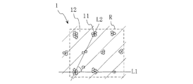
- FIG. 1 is an enlarged top view showing an embodiment of the conductive adhesive sheet of the present invention.
- a plurality of conductive particles 11 are dispersed and arranged in the binder component 12 in the plane direction of the conductive adhesive sheet 1.
- the conductive particles 11 are dispersed and arranged in units of primary particles when the conductive particles are primary particles 11a and in units of aggregates when the conductive particles are aggregates 11b.
- conductive particles when simply referred to as “conductive particles”, the conductive particle units are dispersed and arranged, that is, the primary particles are dispersed and arranged as primary particles, and the primary particles are dispersed and arranged as aggregate units. It shall refer to a collection.
- the number of dispersedly arranged conductive particles is 9 in the state where it is assumed that all the conductive particles are regularly arranged.
- the dispersedly arranged conductive particles 11 are regularly arranged over a plurality of rows. Specifically, in other words, each conductive particle 11 is regularly arranged in the first arrangement direction L1 and the second arrangement direction L2 in which the angle ⁇ with respect to the first arrangement direction L1 is 90 °.
- a plurality of conductive particles 11 are arranged at substantially equal intervals in the first arrangement direction L1, and this row is in the second arrangement direction L2 such that the angle ⁇ formed by the first arrangement direction L1 is 90 °.
- Multiple rows are arranged at approximately equal intervals.
- the first arrangement direction L1 is the direction in which the adjacent conductive particles are arranged at the shortest distance (for example, d1 in FIG. 1) from the arbitrary conductive particles 11.
- the second arrangement direction L2 is an arrangement direction different from the first arrangement direction L1, and is adjacent to any conductive particle 11 at a distance next to d1 or the same distance as d1 (for example, d2 in FIG. 1).
- the direction in which the matching conductive particles are arranged is different from the first arrangement direction L1 and the second arrangement direction L2, and the particles are adjacent to each other at the shortest distance next to d2 or the same distance as d2 (for example, d3 in FIG. 1).
- the direction in which the conductive particles are arranged is defined as the third arrangement direction.
- the conductive particles 11 are regularly arranged in the region R, but in the present invention, the conductive particles 11 may be arranged substantially regularly.
- substantially regularly arranging the particles for example, when some of the conductive particles 11 are slightly deviated from the row as shown in FIG. As shown in the above, there may be a case where a part of the position where the conductive particle 11 should be arranged is missing (missing).
- the angle ⁇ formed by the first arrangement direction L1 and the second arrangement direction L2 is the smaller angle when the two angles formed by the first arrangement direction L1 and the second arrangement direction L2 are different, and is not particularly limited. , 0 to 90 ° can be appropriately selected.
- Examples of the shape in which the angle ⁇ is an acute angle include the arrangement shown in FIG. Among them, in the conductive adhesive sheet of the present invention, a shape having an angle ⁇ of 90 ° (lattice shape) and a shape having an angle ⁇ of 45 ° (houndstooth shape) as shown in FIGS. 1 to 3 are preferable.
- the conductive particles are arranged in a grid pattern, the adhesion to the adherend and the connection stability are improved.
- the conductive adhesive sheet of the present invention corresponds to the distance Y between the centers of the dispersedly arranged conductive particles (d1, d2, or d3 shown in FIG. 1) adjacent to each other in the plane direction and the circle of the dispersedly arranged conductive particles.
- the relationship of the average value X of the diameter satisfies 1.5 ⁇ Y ⁇ 100X.
- 1.5X ⁇ Y the distance between the conductive particles adjacent to each other in the plane direction is sufficiently large, and the conductive particles are appropriately dispersed over the entire conductive adhesive sheet. Adhesion is good.
- Y ⁇ 100X the distance between the dispersed conductive particles is not too large, and the connection stability of the conductive adhesive sheet is excellent.
- the lower limit of the center-to-center distance Y is preferably 3X, more preferably 5X, and even more preferably 7X.
- the upper limit of the center-to-center distance Y is preferably 50X, more preferably 30X, and even more preferably 15X.
- the center-to-center distance d1, the center-to-center distance d2, and the center-to-center distance d3 each satisfy 1.5X ⁇ Y ⁇ 100X.
- the equivalent circle diameter of the conductive particles is the equivalent circle diameter of the primary particles when the dispersed conductive particles are primary particles, and the equivalent circle diameter of the dispersed conductive particles is an aggregate such as secondary particles.
- the circle-equivalent diameter is, for example, within an arbitrary region (for example, FIG. 1) in which the number of dispersed arrangements Np is 9 to 25 in a state (at the time of complete arrangement) assuming that all conductive particles are regularly arranged. In the region R shown in (1), it is calculated by image analysis of an optical micrograph.
- an image of an optical micrograph taken at a magnification within a range of 1 mm ⁇ 1 mm can be captured in a PC, subjected to image processing, and then the equivalent circle diameter can be calculated.
- the Np in the above arbitrary region is preferably 9, 16 or 25 having the same number of distributed arrangements in the first arrangement direction L1 and the second arrangement direction L2.
- the average value X of the equivalent circle diameters of the conductive particles is not particularly limited, but is preferably 2 to 120 ⁇ m, more preferably 15 to 100 ⁇ m, and even more preferably 25 to 80 ⁇ m.
- the conductive adhesive sheet of the present invention has good connection stability with respect to the conventional anisotropic conductive film. Therefore, the conductive adhesive sheet of the present invention having such a configuration can be preferably used for conductive bonding film applications.
- the center-to-center distance Y is, for example, the center-to-center distance (each conductivity) of two conductive particles that are regularly arranged and adjacent to each other in the same arrangement direction in the region R for obtaining the center-to-center distance Y. Particle spacing) Y is calculated.
- the center value of the circle-equivalent diameter of the aggregates is used.
- the coefficient of variation of the center-to-center distance Y is not particularly limited, but is preferably 0.5 or less, and more preferably 0.3 or less.
- the coefficient of variation of the center-to-center distance Y is a measure of the regular arrangement of the dispersed conductive particles.
- the coefficient of variation of the distance Y between the centers of the conductive particles is a value obtained by dividing the standard deviation of the distance between the centers of the conductive particles by the average value.
- the distance d3 may be different from each other, two or more of them may be the same, or all may be the same.
- the center-to-center distances d1, d2, and d3 are preferably 100 to 1000 ⁇ m, more preferably 150 to 800 ⁇ m, and even more preferably 200 to 600 ⁇ m, respectively. When the distance between the centers is within the above range, both the adhesion to the adherend and the connection stability are more excellent.
- the conductive adhesive sheet of the present invention comprises the number (N) of the primary particles of the conductive particles and the conductive particles in a state (at the time of complete arrangement) assuming that all the conductive particles are regularly arranged.
- N / Np is 1.0 or more
- the conductive particles are sufficiently arranged at the planned arrangement position, or the number of conductive particles within a specific range is sufficient, and the connection stability is improved. ..
- the N / Np is 100.0 or less, the excessive aggregation of the conductive particles is suppressed to some extent, so that the adhesion to the adherend is improved and the amount of the conductive particles used can be suppressed. it can.
- the N / Np is obtained in the arbitrary region when the center-to-center distance Y is obtained.
- the N / Np is preferably 1.05 to 50.0, more preferably 1.2 to 30.0, and even more preferably 1.5 to 10.0.
- N / Np is 1.05 or more, the conductive particles dispersed and arranged appropriately contain agglomerates in the conductive adhesive sheet, and the connection stability becomes better.
- the N / Np is 50.0 or less, the excessive aggregation of the conductive particles is further suppressed, so that the adhesion to the adherend becomes better.
- N in the region R is 9 in each case.
- the conductive adhesive sheet of the present invention has two regions out of the above three regions when any three non-overlapping regions including the above arbitrary regions are viewed in a plan view so that the Np of each region is 9 to 25 points.
- Ng / Np is 0.8 to 1.0, preferably 0.85 to 1.0, and more preferably 0.9 to 1. It is 0.
- Ng / Np is 0.8 or more, the proportion of conductive particles that are not arranged in the ideal arrangement and the proportion of conductive particles that are not arranged in the ideal arrangement are small. Good connection stability and adhesion to the adherend. The higher the Ng / Np, the more preferable, and the best is 1.0.
- one region in the three regions when determining Ng / Np is the arbitrary region when determining the center-to-center distance Y, and the other two regions do not include conductive particles in the arbitrary region. Furthermore, it is a region that does not contain conductive particles that overlap each other. Then, for the above three regions, regions having the same Np are selected.
- FIGS. 1 to 3 are enlarged views of different regions in one conductive adhesive sheet of the present invention
- the region R in FIG. 1 The region R in FIG. 2 and the region R in FIG. 3 are three regions when Ng / Np is obtained.
- the number of dispersed arrangements of the conductive particles existing in the two regions is 1, and the number of dispersed arrangements of the conductive particles existing in the three regions is 8, so the number of dispersed arrangements of the conductive particles existing in two or more regions is 9. is there.
- Ng / Np in this case is 1.0.
- the thickness of the portion where the conductive particles are arranged (for example, h1 shown in FIG. 5) is higher than the thickness of the portion where the conductive particles are not arranged (for example, h2 shown in FIG. 5). It is preferable to have a thick portion.
- the conductive adhesive sheet of the present invention has a configuration in which the arrangement portion of the conductive particles protrudes from the contact surface, and the contact frequency of the conductive particles with the adherend is high, and the connection is made. Better stability.
- FIG. 5 is a schematic cross-sectional view showing an embodiment of the conductive adhesive sheet of the present invention.
- the thickness of the conductive adhesive sheet of the present invention can be appropriately selected according to the application.
- the thickness is, for example, 1 to 50 ⁇ m, preferably 5 to 25 ⁇ m.
- the thickness is 1 ⁇ m or more, the embedding property of the printed wiring board into the opening provided in the electromagnetic wave shield laminated body becomes better.
- the thickness is 50 ⁇ m or less, it is possible to meet the demand for thinning.
- the viewpoint suitable for using the conductive adhesive sheet of the present invention as a bonding film it is, for example, 10 to 70 ⁇ m, preferably 30 to 65 ⁇ m.
- the number of conductive particles (primary particles) per unit area is not particularly limited, but is preferably 10 to 1000 particles / mm 2 , and more preferably 20 to 800 particles / mm 2 . More preferably, it is 30 to 600 pieces / mm 2 . When the number per unit area is within the above range, the balance between the connection stability and the adhesion to the adherend becomes better.
- the conductive adhesive sheet of the present invention preferably has an electrical resistance value of 1 ⁇ or less, more preferably 0.5 ⁇ or less, after being heated and pressurized at 170 ° C. and 3.0 MPa.
- binder component examples include thermoplastic resins, thermosetting resins, active energy ray-curable compounds, and the like.
- the binder component only one kind may be used, or two or more kinds may be used.
- thermoplastic resin examples include polystyrene-based resin, vinyl acetate-based resin, polyester-based resin, polyolefin-based resin (for example, polyethylene-based resin, polypropylene-based resin composition, etc.), polyimide-based resin, acrylic-based resin, and the like. Be done.
- thermoplastic resin only one kind may be used, or two or more kinds may be used.
- thermosetting resin examples include both a thermosetting resin (thermosetting resin) and a resin obtained by curing the thermosetting resin.
- thermosetting resin examples include phenolic resin, epoxy resin, urethane resin, melamine resin, alkyd resin and the like. As the thermosetting resin, only one kind may be used, or two or more kinds may be used.
- epoxy resin examples include bisphenol type epoxy resin, spiro ring type epoxy resin, naphthalene type epoxy resin, biphenyl type epoxy resin, terpen type epoxy resin, glycidyl ether type epoxy resin, and glycidyl amine type. Examples thereof include epoxy-based resins and novolac-type epoxy-based resins.
- Examples of the bisphenol type epoxy resin include bisphenol A type epoxy resin, bisphenol F type epoxy resin, bisphenol S type epoxy resin, and tetrabrom bisphenol A type epoxy resin.
- Examples of the glycidyl ether type epoxy resin include tris (glycidyloxyphenyl) methane and tetrakis (glycidyloxyphenyl) ethane.
- Examples of the glycidylamine type epoxy resin include tetraglycidyldiaminodiphenylmethane.
- Examples of the novolak type epoxy resin include cresol novolac type epoxy resin, phenol novolac type epoxy resin, ⁇ -naphthol novolac type epoxy resin, brominated phenol novolac type epoxy resin and the like.
- the active energy ray-curable compound examples include both a compound that can be cured by irradiation with active energy rays (active energy ray curable compound) and a compound obtained by curing the active energy ray curable compound.
- the active energy ray-curable compound is not particularly limited, and examples thereof include a polymerizable compound having at least two radical reactive groups (for example, (meth) acryloyl group) in the molecule.
- the active energy ray-curable compound only one kind may be used, or two or more kinds may be used.
- thermosetting resin a thermosetting resin is preferable.
- the adhesive can be made to flow by pressurization and heating, and then the binder component can be cured.
- a curing agent for accelerating the heat curing reaction may be contained as a component constituting the binder component.
- the curing agent can be appropriately selected depending on the type of the thermosetting resin. As the curing agent, only one kind may be used, or two or more kinds may be used.
- the content ratio of the binder component in the conductive adhesive sheet of the present invention is not particularly limited, but is preferably 40 to 90% by mass, more preferably 45 to 85, based on 100% by mass of the total amount of the conductive adhesive sheet of the present invention. It is by mass, more preferably 50 to 80% by mass. When the content ratio is 40% by mass or more, the adhesion to the adherend and the fluidity at the time of pressurization / heating are excellent. When the content ratio is 90% by mass or less, the conductive particles can be sufficiently contained.
- Examples of the conductive particles include metal particles, metal-coated resin particles, carbon fillers, and the like. As the conductive particles, only one kind may be used, or two or more kinds may be used.
- Examples of the metal constituting the coating portion of the metal particles and the metal-coated resin particles include gold, silver, copper, nickel, zinc, tin, bismuth, and indium. Only one kind of the above metal may be used, or two or more kinds may be used.
- the metal particles include copper particles, silver particles, nickel particles, silver-coated copper particles, gold-coated copper particles, silver-coated nickel particles, gold-coated nickel particles, silver-coated alloy particles, and tin-coated copper.
- examples include particles, tin-coated nickel particles, and solder particles.
- the silver-coated alloy particles include silver-coated copper alloy particles in which alloy particles containing copper (for example, copper alloy particles made of an alloy of copper, nickel, and zinc) are coated with silver.
- the metal particles can be produced by an electrolysis method, an atomizing method, a reduction method or the like.
- silver particles, silver-coated copper particles, silver-coated copper alloy particles, tin-coated copper particles, tin-coated nickel particles, and solder particles are preferable.
- Silver particles, silver-coated copper particles, and silver-coated copper alloy particles are preferable, and silver-coated copper particles are particularly preferable, from the viewpoints of excellent conductivity, suppression of oxidation and aggregation of metal particles, and reduction of cost of metal particles.
- Silver-coated copper alloy particles are preferred.
- tin-coated copper particles, tin-coated nickel particles, and solder particles are preferable from the viewpoint that they can form an alloy with the circuit or ground member of the printed wiring board and can be firmly connected.
- Examples of the shape of the conductive particles include spherical, flake-shaped (scaly), dendritic, fibrous, and amorphous (polyhedron). Among them, spherical, dendritic, and amorphous (polyhedron) are preferable from the viewpoint of lowering the electric resistance value of the conductive adhesive sheet.
- the median diameter (D50) of the conductive particles is not particularly limited, but is preferably 15 to 100 ⁇ m, more preferably 25 to 80 ⁇ m.
- D50 is within the above range, the conductive adhesive sheet of the present invention has good connection stability with respect to the conventional anisotropic conductive film. Therefore, the conductive adhesive sheet of the present invention having such a configuration can be preferably used for conductive bonding film applications.
- the D50 refers to the particle size at an integrated value of 50% in the particle size distribution obtained by the laser diffraction / scattering method.
- the content ratio of the conductive particles in the conductive adhesive sheet of the present invention is not particularly limited, but is preferably 10 to 60% by mass, more preferably 15 to 60% by mass, based on 100% by mass of the total amount of the conductive adhesive sheet of the present invention. It is 55% by mass, more preferably 20 to 50% by mass.
- the content ratio is 10% by mass or more, the connection stability becomes better.
- the content ratio is 60% by mass or less, the adhesion to the adherend becomes better.
- the conductive adhesive sheet of the present invention is used as the conductive bonding film.
- the connection stability is good. Therefore, the conductive adhesive sheet of the present invention having such a configuration can be preferably used for conductive bonding film applications.
- the conductive adhesive sheet of the present invention may contain other components other than the above-mentioned components as long as the effects of the present invention are not impaired.
- the other components include components contained in known or commonly used conductive adhesive sheets.
- the other components include flame retardants, plasticizers, antifoaming agents, viscosity modifiers, antioxidants, diluents, antisettling agents, fillers, colorants, leveling agents, coupling agents, and tackifier resins. And so on.
- flame retardants plasticizers, antifoaming agents, viscosity modifiers, antioxidants, diluents, antisettling agents, fillers, colorants, leveling agents, coupling agents, and tackifier resins. And so on.
- the above other components only one kind may be used, or two or more kinds may be used.
- the conductive adhesive sheet of the present invention can be manufactured by a known or conventional manufacturing method.
- an adhesive composition for forming a conductive adhesive sheet is applied (coated) on a temporary base material such as a separate film or a base material, and if necessary, desolvated and / or partially cured to form the adhesive composition.
- a temporary base material such as a separate film or a base material
- the conductive particles may be embedded at a desired position after the coating of the adhesive composition containing no conductive particles.
- the conductive particles are arranged on the temporary base material or the base material in the arrangement specified in the present invention, and then the adhesive composition containing no conductive particles is applied, and then the solvent is removed as necessary. And / or may be partially cured to form.
- the adhesive composition may contain a solvent (solvent) in addition to each component contained in the conductive adhesive sheet described above, for example.
- solvent include toluene, acetone, methyl ethyl ketone, methanol, ethanol, propanol, dimethylformamide and the like.
- the solid content concentration of the adhesive composition is appropriately set according to the thickness of the conductive adhesive sheet to be formed and the like.
- a known coating method may be used for applying the adhesive composition.
- a coater such as a gravure roll coater, a reverse roll coater, a kiss roll coater, a lip coater, a dip roll coater, a bar coater, a knife coater, a spray coater, a comma coater, a direct coater, or a slot die coater may be used.
- the conductive adhesive sheet of the present invention is preferably used for printed wiring boards, and particularly preferably for conductive bonding films, from the viewpoint of adhesion to an adherend and connection stability.
- the printed wiring board application include a conductive adhesive sheet constituting the electromagnetic wave shield laminate (for example, a conductive adhesive sheet provided on the surface of an insulating protective layer covering a circuit pattern of the printed wiring board) in addition to the conductive bonding film. Be done.
- the conductive bonding film include an FGF adhesive, a bonding film between a reinforcing plate and a printed wiring board, and a bonding film between an external ground and a printed wiring board for grounding a circuit.
- FIG. 6 shows an embodiment of an example in which the conductive adhesive sheet of the present invention is used as a conductive bonding film between a reinforcing plate and a printed wiring board.
- the shield printed wiring board 2 shown in FIG. 6 is filled in the printed wiring board 20, the electromagnetic wave shield laminated body 30 laminated on the printed wiring board 20, and the through holes 33 provided in the electromagnetic wave shield laminated body 30. It includes a conductive adhesive layer 40 and a reinforcing plate 50 bonded by the conductive adhesive layer 40.
- the conductive adhesive layer 40 is formed from the conductive adhesive sheet of the present invention.
- the printed wiring board 20 includes a base member 21, a circuit pattern 23 partially provided on the surface of the base member 21, an insulating protective layer (coverlay) 24 that covers and protects the circuit pattern 23, and a circuit pattern 23. It has a cover and a circuit pattern 23 and an adhesive layer 22 for adhering the base member 21 and the insulating protective layer 24.
- the circuit pattern 23 includes a plurality of signal circuits.
- the electromagnetic wave shield laminate 30 is laminated on the printed wiring board 20, specifically, on the insulating protective layer 24 of the printed wiring board 20, in the order of the conductive adhesive layer 31 and the insulating layer 32.
- the conductive adhesive layer 31 and the insulating layer 32 have through holes 33 that penetrate in the thickness direction (that is, the surface of the printed wiring board 20 is exposed). By having the through hole 33, the conductive adhesive sheet of the present invention flows into the through hole 33 by pressurization and heating to form the conductive adhesive layer 40, and is electrically connected to the conductive adhesive layer 31. can do.
- the bottom of the through hole 33 is a printed wiring board 20, specifically, an insulating protective layer 24.
- the through hole 33 is formed from the side surface of the insulating layer 32, the side surface of the conductive adhesive layer 31, and the surface of the printed wiring board 20 (particularly the insulating protective layer 24).
- the conductive adhesive layer 31 may be the conductive adhesive sheet of the present invention, or may be formed from the conductive adhesive sheet of the present invention (for example, formed by thermocompression bonding). May be good.
- the electromagnetic wave shield laminate 30 can be manufactured by using an electromagnetic wave shield film.
- the electromagnetic wave shielding film may be a shield film having the conductive adhesive sheet of the present invention (electromagnetic wave shielding film of the present invention), for example, a transfer film, an insulating layer (protective layer), a conductive adhesive sheet of the present invention. It has (conductive adhesive layer) and a separate film in this order.
- the electromagnetic wave shield film is used by sticking the exposed surface of the separate film to the surface of the printed wiring board 20, and then the transfer film is peeled off.
- the conductive adhesive layer 40 is arranged on the electromagnetic wave shield laminated body 30, fills the through holes 33, and has an action of electrically connecting to the conductive adhesive layer 31 in the through holes 33.
- the reinforcing plate 50 is fixed to the printed wiring board 20 and the electromagnetic wave shield laminate 30 via the conductive adhesive layer 31.
- the conductive adhesive layer 40 functions as a ground connecting member.
- the conductive adhesive sheet of the present invention can be used.
- the ground connecting member is a ground connecting member having the conductive adhesive sheet of the present invention (ground connecting member of the present invention), and a conductor such as a metal layer may be laminated on the conductive adhesive sheet of the present invention.
- the conductive adhesive layer 40 is not in contact with the circuit pattern.
- the height of the adhesive forming the conductive adhesive layer 40 flowing into the through hole is low, it is possible to prevent air bubbles from being mixed due to insufficient inflow into the through hole. Therefore, for example, interfacial peeling in the reflow process can be suppressed, and stable connection reliability can be obtained.
- the printed wiring board 20 can have shape retention by using the reinforcing plate 50.
- the shield printed wiring board is preferably a flexible printed wiring board (FPC).
- the shield printed wiring board is a step of laminating a reinforcing plate provided with an electromagnetic bonding film, which is a conductive adhesive sheet of the present invention, on the upper surface of the through hole so that the electromagnetic bonding film comes into contact with the electromagnetic shielding laminate (). (Reinforcing plate laminating process) and thermocompression bonding to allow the electromagnetic bonding film to flow into the through hole to form a conductive adhesive layer, and the conductive adhesive layer in the electromagnetic shielding laminate and the conductivity derived from the electromagnetic bonding film. It can be manufactured by a manufacturing method including a step of abutting the sex adhesive layer (thermocompression bonding step).
- the conductive bonding film which is the conductive adhesive sheet of the present invention, and the reinforcing plate 50 are bonded together, cut to an arbitrary size, and then passed through the surface of the conductive bonding film. It is arranged on the surface of the insulating layer 32 so as to close the opening of the hole 33.
- the conductive bonding film softens and flows by pressurization and heating, and flows into and fills the through hole 33 by the pressure at the time of pressurization.
- the conductive adhesive layer 40 is formed by curing by subsequent cooling or thermal polymerization. In this way, the conductive bonding film flows by thermocompression bonding and comes into contact with the conductive adhesive layer 31.
- Conductive adhesive sheet of the present invention 11 Conductive particles 11a Conductive particles (primary particles) 11b Conductive particles (aggregates) 12 Binder component R region L1 1st arrangement direction L2 2nd arrangement direction ⁇ Angle formed by 1st arrangement direction L1 and 1st arrangement direction L2 d1 Distance between centers of conductive particles adjacent to each other in the 1st arrangement direction d2 2nd arrangement Distance between centers of adjacent conductive particles in the direction d3 Distance between centers of adjacent conductive particles in the third arrangement direction h1 Thickness of the portion where the conductive particles are arranged h2 Thickness of the portion where the conductive particles are not arranged 2 Shielded printed wiring board 20 Printed wiring board 21 Base member 22 Adhesive layer 23 Circuit pattern 24 Insulation protective layer (coverlay) 30 Electromagnetic wave shield laminate 31 Conductive adhesive layer 32 Insulation layer 33 Through hole 40 Conductive adhesive layer 50 Reinforcing plate
Landscapes
- Chemical & Material Sciences (AREA)
- Organic Chemistry (AREA)
- Engineering & Computer Science (AREA)
- Microelectronics & Electronic Packaging (AREA)
- Physics & Mathematics (AREA)
- Dispersion Chemistry (AREA)
- Spectroscopy & Molecular Physics (AREA)
- Inorganic Chemistry (AREA)
- Electromagnetism (AREA)
- Adhesives Or Adhesive Processes (AREA)
- Adhesive Tapes (AREA)
- Conductive Materials (AREA)
Abstract
Description
本発明の導電性接着シートは、バインダー成分及び導電性粒子を含有する。上記導電性粒子は、一次粒子、又は一次粒子の凝集体(二次粒子など)として分散配置されている。上記分散配置された導電性粒子は導電性接着シートを平面視した際に、平面方向に複数列に亘って略規則的に配列している。ここで、全ての導電性粒子が規則的に配列していると仮定した状態の、上記分散配置された導電性粒子の分散配置数Npが9~25箇所となるように導電性接着シートの任意の領域を平面視した際の、上記分散配置された導電性粒子の円相当径の平均値をX、上記平面視した際に規則的に配列した隣り合う上記分散配置された導電性粒子の中心間距離をYとした場合、1.5X≦Y≦100Xを満たす。また、上記任意の領域における上記導電性粒子の一次粒子の個数をNとした場合、N/Npは1.0~100.0である。また、各領域のNpが9~25箇所となるように、上記任意の領域を含む重複しない任意の三領域を平面視した際の、上記三領域のうちの二領域以上に存在する導電性粒子の分散配置数をNgとした場合、Ng/Npが0.8~1.0である。
11 導電性粒子
11a 導電性粒子(一次粒子)
11b 導電性粒子(凝集体)
12 バインダー成分
R 領域
L1 第1配列方向
L2 第2配列方向
α 第1配列方向L1と第1配列方向L2とでなす角度
d1 第1配列方向において隣り合う導電性粒子の中心間距離
d2 第2配列方向において隣り合う導電性粒子の中心間距離
d3 第3配列方向において隣り合う導電性粒子の中心間距離
h1 導電性粒子が配置された部分の厚み
h2 導電性粒子が配置されていない部分の厚み
2 シールドプリント配線板
20 プリント配線板
21 ベース部材
22 接着剤層
23 回路パターン
24 絶縁保護層(カバーレイ)
30 電磁波シールド積層体
31 導電性接着剤層
32 絶縁層
33 スルーホール
40 導電性接着剤層
50 補強板
Claims (9)
- バインダー成分及び導電性粒子を含有する導電性接着シートであり、
前記導電性粒子は、一次粒子又は一次粒子の凝集体として分散配置されており、
全ての導電性粒子が規則的に配列していると仮定した状態の、前記分散配置された導電性粒子の分散配置数Npが9~25箇所となるように前記導電性接着シートの任意の領域を平面視した際の、前記分散配置された導電性粒子の円相当径の平均値をX、前記平面視した際に規則的に配列した隣り合う前記分散配置された導電性粒子の中心間距離をYとした場合、1.5X≦Y≦100Xを満たし、
前記任意の領域における前記一次粒子の個数をNとした場合、N/Npが1.0~100.0であり、
各領域のNpが9~25箇所となるように、前記任意の領域を含む重複しない任意の三領域を平面視した際の、前記三領域のうちの二領域以上に存在する導電性粒子の分散配置数をNgとした場合、Ng/Npが0.8~1.0である、導電性接着シート。 - 前記N/Npが1.05~50.0である請求項1に記載の導電性接着シート。
- 前記中心間距離Yの変動係数が0.5以下である請求項1又は2に記載の導電性接着シート。
- 前記バインダー成分として熱硬化性樹脂を含む請求項1~3のいずれか1項に記載の導電性接着シート。
- 前記導電性粒子の含有割合が前記導電性接着シートの総量100質量%に対して10~60質量%である請求項1~4のいずれか1項に記載の導電性接着シート。
- 前記導電性粒子が分散配置された部分の厚みが、前記導電性粒子が配置されていない部分の厚みよりも厚い部分を有する請求項1~5のいずれか1項に記載の導電性接着シート。
- 前記円相当径の平均値Xが2~120μmである請求項1~6のいずれか1項に記載の導電性接着シート。
- 請求項1~7のいずれか1項に記載の導電性接着シートを有する電磁波シールドフィルム。
- 請求項1~7のいずれか1項に記載の導電性接着シートを有するグランド接続部材。
Priority Applications (5)
| Application Number | Priority Date | Filing Date | Title |
|---|---|---|---|
| US17/612,398 US20220220346A1 (en) | 2019-05-20 | 2020-05-20 | Conductive Adhesive Sheet |
| KR1020217040612A KR102404193B1 (ko) | 2019-05-20 | 2020-05-20 | 도전성 접착 시트 |
| CN202080036671.7A CN113811583A (zh) | 2019-05-20 | 2020-05-20 | 导电性接合片 |
| JP2020548839A JP6794591B1 (ja) | 2019-05-20 | 2020-05-20 | 導電性接着シート |
| US18/417,803 US12526924B2 (en) | 2019-05-20 | 2024-01-19 | Conductive adhesive sheet |
Applications Claiming Priority (2)
| Application Number | Priority Date | Filing Date | Title |
|---|---|---|---|
| JP2019-094741 | 2019-05-20 | ||
| JP2019094741 | 2019-05-20 |
Related Child Applications (2)
| Application Number | Title | Priority Date | Filing Date |
|---|---|---|---|
| US17/612,398 A-371-Of-International US20220220346A1 (en) | 2019-05-20 | 2020-05-20 | Conductive Adhesive Sheet |
| US18/417,803 Continuation US12526924B2 (en) | 2019-05-20 | 2024-01-19 | Conductive adhesive sheet |
Publications (1)
| Publication Number | Publication Date |
|---|---|
| WO2020235573A1 true WO2020235573A1 (ja) | 2020-11-26 |
Family
ID=73459431
Family Applications (1)
| Application Number | Title | Priority Date | Filing Date |
|---|---|---|---|
| PCT/JP2020/019842 Ceased WO2020235573A1 (ja) | 2019-05-20 | 2020-05-20 | 導電性接着シート |
Country Status (6)
| Country | Link |
|---|---|
| US (2) | US20220220346A1 (ja) |
| JP (1) | JP6794591B1 (ja) |
| KR (1) | KR102404193B1 (ja) |
| CN (1) | CN113811583A (ja) |
| TW (1) | TWI800728B (ja) |
| WO (1) | WO2020235573A1 (ja) |
Cited By (3)
| Publication number | Priority date | Publication date | Assignee | Title |
|---|---|---|---|---|
| WO2023136299A1 (ja) * | 2022-01-14 | 2023-07-20 | 学校法人早稲田大学 | 接着層の接着強度を低下させる方法 |
| WO2023182329A1 (ja) * | 2022-03-24 | 2023-09-28 | タツタ電線株式会社 | 熱伝導性導電層 |
| US12526924B2 (en) | 2019-05-20 | 2026-01-13 | Tatsuta Electric Wire & Cable Co., Ltd. | Conductive adhesive sheet |
Families Citing this family (1)
| Publication number | Priority date | Publication date | Assignee | Title |
|---|---|---|---|---|
| KR102597774B1 (ko) * | 2023-02-20 | 2023-11-03 | (주)켐코스 | 전자파 차폐필름 및 이의 제조방법 |
Citations (3)
| Publication number | Priority date | Publication date | Assignee | Title |
|---|---|---|---|---|
| JP2003220669A (ja) * | 2002-01-29 | 2003-08-05 | Asahi Kasei Corp | 異方性を有する導電性接着シートおよびその製造方法 |
| JP2018078096A (ja) * | 2016-10-31 | 2018-05-17 | デクセリアルズ株式会社 | フィラー含有フィルム |
| JP2019029135A (ja) * | 2017-07-27 | 2019-02-21 | 日立化成株式会社 | 異方性導電フィルム及びその製造方法、並びに接続構造体及びその製造方法 |
Family Cites Families (13)
| Publication number | Priority date | Publication date | Assignee | Title |
|---|---|---|---|---|
| JP5581605B2 (ja) * | 2009-04-16 | 2014-09-03 | デクセリアルズ株式会社 | 異方導電性接着フィルムの製造方法 |
| US9469790B2 (en) * | 2009-09-29 | 2016-10-18 | The Boeing Company | Adhesive compositions comprising electrically insulating-coated carbon-based particles and methods for their use and preparation |
| JP2012164454A (ja) * | 2011-02-04 | 2012-08-30 | Sony Chemical & Information Device Corp | 導電性粒子及びこれを用いた異方性導電材料 |
| CN103597551B (zh) | 2011-05-31 | 2016-04-06 | 东洋油墨Sc控股株式会社 | 导电性片及其制造方法以及电子零件 |
| JP6119718B2 (ja) * | 2013-11-19 | 2017-04-26 | デクセリアルズ株式会社 | 異方導電性フィルム及び接続構造体 |
| JP6241326B2 (ja) * | 2014-03-07 | 2017-12-06 | デクセリアルズ株式会社 | 異方性導電フィルム及びその製造方法 |
| CN110265174B (zh) * | 2015-01-13 | 2022-06-28 | 迪睿合株式会社 | 各向异性导电性膜 |
| US20180022968A1 (en) * | 2015-03-20 | 2018-01-25 | Dexerials Corporation | Anisotropic conductive film and connection structure |
| CN108028477A (zh) * | 2015-10-07 | 2018-05-11 | 迪睿合株式会社 | 各向异性导电膜和连接结构体 |
| JP2018039959A (ja) * | 2016-09-09 | 2018-03-15 | タツタ電線株式会社 | 導電性接着剤組成物 |
| CN114907594B (zh) * | 2016-10-31 | 2025-07-22 | 迪睿合株式会社 | 含填料膜 |
| JP6431998B1 (ja) * | 2018-03-20 | 2018-11-28 | タツタ電線株式会社 | 導電性接着剤層 |
| TWI800728B (zh) | 2019-05-20 | 2023-05-01 | 日商拓自達電線股份有限公司 | 導電性接著片 |
-
2020
- 2020-05-20 TW TW109116756A patent/TWI800728B/zh active
- 2020-05-20 CN CN202080036671.7A patent/CN113811583A/zh active Pending
- 2020-05-20 US US17/612,398 patent/US20220220346A1/en not_active Abandoned
- 2020-05-20 KR KR1020217040612A patent/KR102404193B1/ko active Active
- 2020-05-20 JP JP2020548839A patent/JP6794591B1/ja active Active
- 2020-05-20 WO PCT/JP2020/019842 patent/WO2020235573A1/ja not_active Ceased
-
2024
- 2024-01-19 US US18/417,803 patent/US12526924B2/en active Active
Patent Citations (3)
| Publication number | Priority date | Publication date | Assignee | Title |
|---|---|---|---|---|
| JP2003220669A (ja) * | 2002-01-29 | 2003-08-05 | Asahi Kasei Corp | 異方性を有する導電性接着シートおよびその製造方法 |
| JP2018078096A (ja) * | 2016-10-31 | 2018-05-17 | デクセリアルズ株式会社 | フィラー含有フィルム |
| JP2019029135A (ja) * | 2017-07-27 | 2019-02-21 | 日立化成株式会社 | 異方性導電フィルム及びその製造方法、並びに接続構造体及びその製造方法 |
Cited By (3)
| Publication number | Priority date | Publication date | Assignee | Title |
|---|---|---|---|---|
| US12526924B2 (en) | 2019-05-20 | 2026-01-13 | Tatsuta Electric Wire & Cable Co., Ltd. | Conductive adhesive sheet |
| WO2023136299A1 (ja) * | 2022-01-14 | 2023-07-20 | 学校法人早稲田大学 | 接着層の接着強度を低下させる方法 |
| WO2023182329A1 (ja) * | 2022-03-24 | 2023-09-28 | タツタ電線株式会社 | 熱伝導性導電層 |
Also Published As
| Publication number | Publication date |
|---|---|
| US20220220346A1 (en) | 2022-07-14 |
| KR20210153767A (ko) | 2021-12-17 |
| US20240158676A1 (en) | 2024-05-16 |
| CN113811583A (zh) | 2021-12-17 |
| JP6794591B1 (ja) | 2020-12-02 |
| KR102404193B1 (ko) | 2022-05-30 |
| US12526924B2 (en) | 2026-01-13 |
| TWI800728B (zh) | 2023-05-01 |
| JPWO2020235573A1 (ja) | 2021-06-10 |
| TW202100342A (zh) | 2021-01-01 |
Similar Documents
| Publication | Publication Date | Title |
|---|---|---|
| JP6794591B1 (ja) | 導電性接着シート | |
| KR102585009B1 (ko) | 전자파 차폐 필름 | |
| CN116096561A (zh) | 电磁波屏蔽膜及屏蔽印制线路板 | |
| KR20220124684A (ko) | 전자파 차폐 필름 | |
| US11597858B1 (en) | Conductive adhesive | |
| JP7617074B2 (ja) | 電磁波シールドフィルム | |
| JP7506150B2 (ja) | 電磁波シールドフィルム | |
| US20240182759A1 (en) | Electroconductive adhesive layer | |
| JP6991400B1 (ja) | グランド接続引き出しフィルム | |
| US20250197694A1 (en) | Thermally-conductive electrical conducting layer | |
| US20250223471A1 (en) | Conductive adhesive layer and heat dissipation structure | |
| WO2025205404A1 (ja) | 熱伝導性導電接着剤層 | |
| CN119604949A (zh) | 导电性粘接剂层 |
Legal Events
| Date | Code | Title | Description |
|---|---|---|---|
| ENP | Entry into the national phase |
Ref document number: 2020548839 Country of ref document: JP Kind code of ref document: A |
|
| 121 | Ep: the epo has been informed by wipo that ep was designated in this application |
Ref document number: 20810165 Country of ref document: EP Kind code of ref document: A1 |
|
| NENP | Non-entry into the national phase |
Ref country code: DE |
|
| ENP | Entry into the national phase |
Ref document number: 20217040612 Country of ref document: KR Kind code of ref document: A |
|
| 122 | Ep: pct application non-entry in european phase |
Ref document number: 20810165 Country of ref document: EP Kind code of ref document: A1 |