WO2020230541A1 - 電力変換装置 - Google Patents
電力変換装置 Download PDFInfo
- Publication number
- WO2020230541A1 WO2020230541A1 PCT/JP2020/017135 JP2020017135W WO2020230541A1 WO 2020230541 A1 WO2020230541 A1 WO 2020230541A1 JP 2020017135 W JP2020017135 W JP 2020017135W WO 2020230541 A1 WO2020230541 A1 WO 2020230541A1
- Authority
- WO
- WIPO (PCT)
- Prior art keywords
- circuit board
- control circuit
- power conversion
- base
- conversion device
- Prior art date
- Legal status (The legal status is an assumption and is not a legal conclusion. Google has not performed a legal analysis and makes no representation as to the accuracy of the status listed.)
- Ceased
Links
Images




Classifications
-
- H—ELECTRICITY
- H02—GENERATION; CONVERSION OR DISTRIBUTION OF ELECTRIC POWER
- H02M—APPARATUS FOR CONVERSION BETWEEN AC AND AC, BETWEEN AC AND DC, OR BETWEEN DC AND DC, AND FOR USE WITH MAINS OR SIMILAR POWER SUPPLY SYSTEMS; CONVERSION OF DC OR AC INPUT POWER INTO SURGE OUTPUT POWER; CONTROL OR REGULATION THEREOF
- H02M7/00—Conversion of AC power input into DC power output; Conversion of DC power input into AC power output
- H02M7/42—Conversion of DC power input into AC power output without possibility of reversal
- H02M7/44—Conversion of DC power input into AC power output without possibility of reversal by static converters
- H02M7/48—Conversion of DC power input into AC power output without possibility of reversal by static converters using discharge tubes with control electrode or semiconductor devices with control electrode
- H02M7/53—Conversion of DC power input into AC power output without possibility of reversal by static converters using discharge tubes with control electrode or semiconductor devices with control electrode using devices of a triode or transistor type requiring continuous application of a control signal
- H02M7/537—Conversion of DC power input into AC power output without possibility of reversal by static converters using discharge tubes with control electrode or semiconductor devices with control electrode using devices of a triode or transistor type requiring continuous application of a control signal using semiconductor devices only, e.g. single switched pulse inverters
- H02M7/5387—Conversion of DC power input into AC power output without possibility of reversal by static converters using discharge tubes with control electrode or semiconductor devices with control electrode using devices of a triode or transistor type requiring continuous application of a control signal using semiconductor devices only, e.g. single switched pulse inverters in a bridge configuration
-
- H—ELECTRICITY
- H02—GENERATION; CONVERSION OR DISTRIBUTION OF ELECTRIC POWER
- H02M—APPARATUS FOR CONVERSION BETWEEN AC AND AC, BETWEEN AC AND DC, OR BETWEEN DC AND DC, AND FOR USE WITH MAINS OR SIMILAR POWER SUPPLY SYSTEMS; CONVERSION OF DC OR AC INPUT POWER INTO SURGE OUTPUT POWER; CONTROL OR REGULATION THEREOF
- H02M1/00—Details of apparatus for conversion
- H02M1/08—Circuits specially adapted for the generation of control voltages for semiconductor devices incorporated in static converters
-
- H—ELECTRICITY
- H02—GENERATION; CONVERSION OR DISTRIBUTION OF ELECTRIC POWER
- H02M—APPARATUS FOR CONVERSION BETWEEN AC AND AC, BETWEEN AC AND DC, OR BETWEEN DC AND DC, AND FOR USE WITH MAINS OR SIMILAR POWER SUPPLY SYSTEMS; CONVERSION OF DC OR AC INPUT POWER INTO SURGE OUTPUT POWER; CONTROL OR REGULATION THEREOF
- H02M1/00—Details of apparatus for conversion
- H02M1/44—Circuits or arrangements for compensating for electromagnetic interference in converters or inverters
-
- H—ELECTRICITY
- H02—GENERATION; CONVERSION OR DISTRIBUTION OF ELECTRIC POWER
- H02M—APPARATUS FOR CONVERSION BETWEEN AC AND AC, BETWEEN AC AND DC, OR BETWEEN DC AND DC, AND FOR USE WITH MAINS OR SIMILAR POWER SUPPLY SYSTEMS; CONVERSION OF DC OR AC INPUT POWER INTO SURGE OUTPUT POWER; CONTROL OR REGULATION THEREOF
- H02M7/00—Conversion of AC power input into DC power output; Conversion of DC power input into AC power output
- H02M7/003—Constructional details, e.g. physical layout, assembly, wiring or busbar connections
-
- H—ELECTRICITY
- H02—GENERATION; CONVERSION OR DISTRIBUTION OF ELECTRIC POWER
- H02M—APPARATUS FOR CONVERSION BETWEEN AC AND AC, BETWEEN AC AND DC, OR BETWEEN DC AND DC, AND FOR USE WITH MAINS OR SIMILAR POWER SUPPLY SYSTEMS; CONVERSION OF DC OR AC INPUT POWER INTO SURGE OUTPUT POWER; CONTROL OR REGULATION THEREOF
- H02M7/00—Conversion of AC power input into DC power output; Conversion of DC power input into AC power output
- H02M7/42—Conversion of DC power input into AC power output without possibility of reversal
- H02M7/44—Conversion of DC power input into AC power output without possibility of reversal by static converters
- H02M7/48—Conversion of DC power input into AC power output without possibility of reversal by static converters using discharge tubes with control electrode or semiconductor devices with control electrode
- H02M7/53—Conversion of DC power input into AC power output without possibility of reversal by static converters using discharge tubes with control electrode or semiconductor devices with control electrode using devices of a triode or transistor type requiring continuous application of a control signal
- H02M7/537—Conversion of DC power input into AC power output without possibility of reversal by static converters using discharge tubes with control electrode or semiconductor devices with control electrode using devices of a triode or transistor type requiring continuous application of a control signal using semiconductor devices only, e.g. single switched pulse inverters
-
- H—ELECTRICITY
- H02—GENERATION; CONVERSION OR DISTRIBUTION OF ELECTRIC POWER
- H02M—APPARATUS FOR CONVERSION BETWEEN AC AND AC, BETWEEN AC AND DC, OR BETWEEN DC AND DC, AND FOR USE WITH MAINS OR SIMILAR POWER SUPPLY SYSTEMS; CONVERSION OF DC OR AC INPUT POWER INTO SURGE OUTPUT POWER; CONTROL OR REGULATION THEREOF
- H02M1/00—Details of apparatus for conversion
- H02M1/32—Means for protecting converters other than automatic disconnection
- H02M1/327—Means for protecting converters other than automatic disconnection against abnormal temperatures
-
- H—ELECTRICITY
- H02—GENERATION; CONVERSION OR DISTRIBUTION OF ELECTRIC POWER
- H02P—CONTROL OR REGULATION OF ELECTRIC MOTORS, ELECTRIC GENERATORS OR DYNAMO-ELECTRIC CONVERTERS; CONTROLLING TRANSFORMERS, REACTORS OR CHOKE COILS
- H02P27/00—Arrangements or methods for the control of AC motors characterised by the kind of supply voltage
- H02P27/04—Arrangements or methods for the control of AC motors characterised by the kind of supply voltage using variable-frequency supply voltage, e.g. inverter or converter supply voltage
- H02P27/06—Arrangements or methods for the control of AC motors characterised by the kind of supply voltage using variable-frequency supply voltage, e.g. inverter or converter supply voltage using DC to AC converters or inverters
Definitions
- the present invention relates to a power conversion device.
- a power conversion device such as an inverter for driving a motor includes a capacitor for smoothing DC power, a semiconductor module having a power conversion circuit for converting DC power to AC power, and a capacitor and a power module in a metal case. It has a structure in which a bus bar connected to a DC power supply is housed.
- a control circuit board is arranged above the power module, a capacitor is arranged on the side of the power module, and a capacitor and power are provided by a positive electrode side bus bar and a negative electrode side bus bar connected to a DC power supply.
- the structure connected to the module is known.
- the positive and negative bus bars are integrated with resin and are connected to the positive electrode side terminal or the negative electrode side terminal of the power module, respectively.
- the connection portion between the positive / negative electrode side bus bar and the positive / negative electrode side terminal of the power module is arranged at a position close to the control circuit board and directly facing the control circuit board (for example, the figure of Patent Document 1). See 2nd class).
- the power conversion device includes a semiconductor module having a power conversion circuit unit, a capacitor that smoothes DC power and supplies it to the power conversion circuit unit, and a control circuit that controls the power conversion circuit unit.
- the control circuit board is electrically connected to the grounding portion of the control circuit board, the control circuit board arranged apart from the capacitor, the connecting conductor connecting the semiconductor module and the capacitor, and the control circuit board.
- the base is electrically connected to the base and has a conductive portion extending in the stacking direction of the base and the control circuit board, and the connecting conductor bypasses the conductive portion. It is connected to a semiconductor module.
- the present invention it is possible to reduce the stray capacitance between the positive / negative side bus bars and the control circuit board, and reduce the EMC (Electromagnetic Compatibility) noise current flowing through the control circuit board.
- EMC Electromagnetic Compatibility
- FIG. 1 is a diagram showing an example of a circuit diagram of the power conversion device of the present invention.
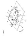
- FIG. 2 is an external perspective view of a power conversion device according to an embodiment of the present invention.
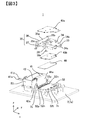
- FIG. 3 is an exploded perspective view of the power conversion device shown in FIG.
- FIG. 4 is a perspective view showing a connection structure between the capacitor of the power conversion device shown in FIG. 2 and the connection conductor.
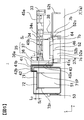
- FIG. 5 is a sectional view taken along line VV of the power conversion device shown in FIG.
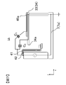
- FIG. 6 is a schematic diagram showing the flow of EMC noise current in the power conversion device shown in FIG.
- FIG. 7 is a diagram showing a flow of EMC noise current of the power conversion device of the comparative example.
- FIG. 8 is a diagram showing a flow of EMC noise current of the power conversion device shown in FIG.
- FIG. 1 is a diagram showing an example of a circuit diagram of the power conversion device of the present invention.
- the power conversion device 1 includes an inverter main circuit 3 that converts DC power into AC power, a noise filter circuit unit 20 for suppressing electromagnetic noise generated when the inverter main circuit 3 performs power conversion operation, and a control unit 170. Be prepared.
- the power conversion device 1 illustrated in FIG. 1 includes a configuration surrounded by a frame including an inverter main circuit 3, a noise filter circuit unit 20, and a control unit 170.
- the inverter main circuit 3 is composed of a power conversion circuit unit 4 that converts DC power into AC power and a capacitor circuit unit 5 that smoothes DC power.
- the power conversion circuit unit 4 has three upper and lower arm series circuits 4a, 4b, and 4c.
- Each of the upper and lower arm series circuits 4a, 4b, and 4c includes a switching element 328 and a diode 156 such as an IGBT (insulated gate type bipolar transistor) that operates as an upper arm, and a switching element 330 and a diode 166 such as an IGBT that operates as a lower arm.
- the switching element 328 of the upper arm and the switching element 330 of the lower arm convert DC power into AC power.
- the diodes 156 and 166 also have a function of converting AC power into DC power during regeneration.
- the upper and lower arm series circuit 4a is connected to the u phase of the motor generator MG via the AC terminal 270a.
- the upper and lower arm series circuit 4b is connected to the v phase of the motor generator MG via the AC terminal 270a.
- the upper and lower arm series circuit 4c is connected to the w phase of the motor generator MG via the AC terminal 270a.
- the motor generator MG outputs the driving force of the HEV or EV based on the AC power supplied from the inverter main circuit 3 via the AC terminal 270a.
- the motor generator MG also acts as a generator that regenerates the AC power when the motor is rotated by an external force to the high voltage battery 2.
- the high voltage battery 2 is an HEV or an EV DC power source.
- the capacitor circuit unit 5 has a capacitor (capacitor) 51, is connected between the high voltage battery 2 and the power conversion circuit unit 4, smoothes the DC power, and supplies the DC power to the power conversion circuit unit 4.
- the noise filter circuit unit 20 is provided between the DC power supply terminal 6 and the capacitor circuit unit 5, and the power conversion circuit unit 4 suppresses electromagnetic noise generated during the power conversion operation.
- the noise filter circuit unit 20 includes a connecting conductor 10, an X capacitor 31, positive and negative Y capacitors 32p and 32n, and a core member 21.
- the connecting conductor 10 is a power transmission path that connects the high-voltage battery 2 and the capacitor circuit unit 5.
- the connecting conductor 10 includes a positive electrode side connecting conductor 10p and a negative electrode side connecting conductor 10n.
- the positive and negative electrode side connecting conductors 10p and 10n are connected to the positive and negative electrode side terminals of the high voltage battery 2 via the positive electrode side DC power supply terminal 6p and the negative electrode side DC power supply terminal 6n, respectively.
- the X capacitor 31 is provided between the positive electrode side connecting conductor 10p and the negative electrode side connecting conductor 10n, and smoothes power having a frequency higher than the power frequency smoothed by the capacitor circuit unit 5.
- the positive and negative electrode side Y capacitors 32p and 32n are provided between the positive electrode side connecting conductor 10p and the ground terminal 134, or between the negative electrode side connecting conductor 10n and the ground terminal 134, respectively, to smooth the electric power.
- the core member 21 suppresses electromagnetic noise by absorbing fluctuations in the current flowing through the connecting conductor 10.
- the positive electrode side terminal of the capacitor circuit unit 5 is connected to the collector of the switching element 328 of each upper arm and the cathode of the diode 156 by the positive electrode side connecting conductor 10p. Further, the negative electrode side terminal of the capacitor 51 is connected to the emitter of the switching element 330 of each lower arm and the anode of the diode 166 by the negative electrode side connecting conductor 10n.
- the control unit 170 includes a driver circuit 174 that drives and controls two power conversion circuit units 4, and a control circuit 172 that supplies a control signal to the driver circuit 174 via a signal line (bus line) 176.
- the gate terminals and emitter sense terminals of the IGBTs 328 and 330 of the upper and lower arm series circuits 4a, 4b, and 4c, respectively, are connected to the control unit 170.
- the upper and lower arm series circuits 4a, 4b, and 4c operate in response to the drive signal output from the control unit 170, and convert the DC power supplied from the high-voltage battery 2 into three-phase AC power. This converted power is supplied to the armature winding of the motor generator MG.
- the control circuit 172 includes a microcomputer for arithmetically processing the switching timings of the IGBTs 328 and 330.
- the target torque value required for the motor generator MG As input information to the microcomputer, the target torque value required for the motor generator MG, the current value supplied from the upper and lower arm series circuits 4a, 4b, and 4c to the armature winding of the motor generator MG, and the motor generator MG.
- the magnetic pole position of the rotor of is input.
- the target torque value is based on a command signal output from a higher-level control device (not shown).
- the current value is detected based on the detection signal output from the current sensor (not shown).
- the magnetic pole position is detected based on a detection signal output from a rotating magnetic pole sensor (not shown) provided in the motor generator MG.
- FIG. 2 is an external perspective view of a power conversion device according to an embodiment of the present invention.
- the power conversion device 1 has a housing formed by a case 7 and a cover (not shown).
- FIG. 2 shows a state in which the cover is removed from the case 7.
- the side wall for forming the storage portion is omitted, and only the bottom portion 7a of the storage portion is shown.
- the x-direction, y-direction, and z-direction are as shown in the figure.
- the case 7 is made of a metal such as an aluminum alloy.
- the case 7 is provided with a capacitor storage portion 53 at a substantially central portion in the width direction (y direction), and is separated from the capacitor storage portion 53 and has a base 33 on one side (right side in the drawing) in the longitudinal direction (x direction). Is placed.
- a plurality of capacitor elements 51a constituting the capacitor 51 are housed in the capacitor storage unit 53.
- a control circuit board 45a is arranged on the base 33, and is fixed to the base 33 by a fastening member 61 such as a screw.
- FIG. 3 is an exploded perspective view of the power conversion device shown in FIG. 2, and FIG. 4 is a perspective view showing a connection structure between the capacitor and the connecting conductor of the power conversion device shown in FIG.
- FIG. 5 is a sectional view taken along line VV of the power conversion device shown in FIG.
- the base 33 is made of a conductive metal such as an aluminum alloy, iron or copper.
- the base 33 has a substantially flat support portion 34, a conductive portion 35 extending in a direction substantially perpendicular to the xy surface of the support portion 34 (z direction), and the support portion 34 toward the bottom 7a side of the case 7. It has a plurality of mounting legs 38 that are extended.
- the control circuit board 45a is laminated above the support portion 34 of the base 33, and the control circuit board 45b is laminated below the support portion 34 of the base 33. That is, the control circuit board 45a and the control circuit board 45b are superposed on the support portion 34 of the base 33.
- the control circuit board 45a and the control circuit board 45b have the control circuit 172 shown in FIG.
- the conductive portion 35 extends in the stacking direction (z direction) of the support portion 34 of the base 33 and the control circuit boards 45a and 45b. As shown in FIG. 3, the conductive portion 35 is provided on both ends of the wide portion 35a extending in the y direction along one side side of the support portion 34 and the wide portion 35a. It has a pair of side portions 35b and 35c extending in the ⁇ x direction (capacitor 51 side) substantially at right angles to the surface.
- the conductive portion 35 has a first conductive portion 36 extending from the support portion 34 to the upper side (+ z direction) side and a second conductive portion 37 extending from the support portion 34 to the lower portion ( ⁇ z direction) side.
- the pair of side portions 35b and 35c are provided on both the first conductive portion 36 and the second conductive portion 37.
- a mounting hole 38a (see FIG. 3) is provided at the tip of each mounting leg 38.
- the base 33 is fixed to the boss portion 7b provided in the case 7 as shown in FIG. 2 by inserting a fastening member (not shown) such as a screw or a bolt into the mounting hole 38a of the mounting leg 38.
- a fastening member such as a screw or a bolt
- the semiconductor module 52 is arranged below the support portion 34 of the base 33, and is fixed to the fixing portion 7c provided on the bottom portion 7a of the case 7.
- the semiconductor module 52 has the upper and lower arm series circuits 4a, 4b, and 4c shown in FIG. As shown in FIG. 3, the semiconductor module 52 has a positive electrode DC terminal 52p, a negative electrode DC terminal 52n, and an AC terminal 52t, respectively, of the upper and lower arm series circuits 4a, 4b, and 4c.
- a drive circuit board 46 is arranged between the support portion 34 of the base 33 and the semiconductor module 52.
- the drive circuit board 46 has the driver circuit 174 shown in FIG.
- the positive electrode side bus bar 41 and the negative electrode side bus bar 42 connect the capacitor 51 and the semiconductor module 52 (see FIG. 3).
- the positive electrode side bus bar 41 and the negative electrode side bus bar 42 correspond to the positive electrode side connecting conductor 10p and the negative electrode side connecting conductor 10n shown in FIG. 1, respectively.
- the capacitor 51 and the base 33 form an EMC noise reduction structure described below.
- the positive electrode side bus bar 41 is connected to the positive electrode side DC power supply terminal 6p (see FIG. 1) of the DC power supply terminal 6 by the positive electrode terminal 41p on one end side, and the positive electrode terminal (shown) of the capacitor 51 at the connection portion 71 (see FIG. 5). It is connected to each positive electrode DC terminal 52p (see FIG. 3) of the semiconductor module 52 at the connection end 41c (see FIG. 4) on the other end side.
- the negative electrode side bus bar 42 is connected to the negative electrode side DC power supply terminal 6n (see FIG. 1) of the DC power supply terminal 6 by the negative electrode terminal 41n on one end side, and the negative electrode terminal (shown) of the capacitor 51 at the connection portion 72 (see FIG. 5).
- each negative electrode DC of the semiconductor module 52 is connected to the connection end portion 42c (see FIG. 4) on the other end side. It is connected to the terminal 52n (see FIG. 3). From the AC terminal 52t of the semiconductor module 52, the AC power obtained by the upper and lower arm series circuits 4a, 4b, and 4c is output.
- the positive and negative electrode side bus bars 41 and 42 are arranged apart from the conductive portion 35 of the base 33 in the longitudinal direction (x direction). Further, as shown in FIG. 2, the length of the positive / negative electrode side bus bars 41 and 42 in the width direction (y direction) is formed to be slightly shorter than the length between the pair of side portions 35b and 35c of the conductive portion 35. The positive and negative bus bars 41 and 42 are arranged apart from each of the side portions 35b and 35c of the conductive portion 35.
- a resin 43 (see FIG. 5) is interposed between the positive electrode side bus bar 41 and the negative electrode side bus bar 42, and the positive electrode side bus bar 41 and the negative electrode side bus bar 42 are insulated by the resin 43.
- the positive electrode side bus bar 41 and the negative electrode side bus bar 42 can be configured as a molded bus bar body integrated with the resin 43 by insert molding.
- the positive and negative side bus bars 41 and 42 have falling portions 41a and 42a, respectively.
- the falling portions 41a and 42a extend downward ( ⁇ z direction) side along the conductive portion 35 substantially parallel to the conductive portion 35 from the upper end 36a side of the first conductive portion 36.
- the positive and negative electrode side bus bars 41 and 42 are below the lower end 37a of the second conductive portion 37, and are fastening members such as screws and bolts to the positive and negative electrode DC terminals 52p and 52n of the semiconductor module 52, respectively (not shown). Is fixed by.
- the capacitor 51 is composed of a plurality of capacitor elements 51a.
- the plurality of capacitor elements 51a are electrically connected in parallel by the positive / negative electrode side terminals 71p and 72n of the positive / negative electrode side connecting portions 71 and 72 of the positive / negative electrode side bus bars 41 and 42.
- the positive electrode side bus bar 41 is illustrated as a structure arranged above the negative electrode side bus bar 42 (+ z direction), but the negative electrode side bus bar 42 is above the positive electrode side bus bar 41 (+ z direction).
- the structure may be arranged on the side.
- the upper end 36a of the first conductive portion 36 of the conductive portion 35 is above (+ z direction) the connecting portions 71 and 72 in which the positive and negative electrode side bus bars 41 and 42 are connected to the capacitor 51. It is extended to.
- control circuit board 45a is attached to the upper portion (+ z direction) side of the support portion 34 of the base 33.
- a control circuit board 45b is attached to the lower portion (-z direction) side of the support portion 34 of the base 33.
- the control circuit board 45a is arranged below the upper end 36a of the first conductive portion 36 of the conductive portion 35 (in the ⁇ z direction), in other words, on the support portion 34 side.
- the control circuit board 45b is arranged above the lower end 37a of the second conductive portion 37 of the conductive portion 35 (in the + z direction), in other words, on the support portion 34 side.
- the semiconductor module 52 has a metal case having good thermal conductivity such as an aluminum alloy.
- the metal case of the semiconductor module 52 has a pair of rectangular wide surfaces 52a and 52b and two pairs of narrow outer peripheral side surfaces provided between the peripheral portions of the wide surfaces 52a and 52b. It has 52c. That is, the outer peripheral side surface 52c is composed of four rectangular side surfaces.
- One wide surface 52a of the metal case of the semiconductor module 52 is thermally conductively coupled to, that is, thermally coupled to the fixing portion 7c provided on the bottom portion 7a of the case 7.
- the case 7 is formed with a cooling flow path through which a refrigerant such as cooling water flows, and the semiconductor module 52 is cooled via the fixing portion 7c of the case 7. Cooling fins may be formed on the wide surface 52a of the semiconductor module 52.
- the capacitor 51 is arranged on the left side ( ⁇ x direction) of the conductive portion 35 extending in the vertical direction (z direction).
- Control circuit boards 45a and 45b laminated on the support portion 34 of the base 33 are arranged on the right side (+ direction) of the conductive portion 35.
- the semiconductor module 52 is arranged in the region between the support portion 34 of the base 33 and the bottom portion 7a of the case 7.
- the semiconductor module 52 is arranged so that the wide surface 52a is in contact with the bottom portion 7a of the case 7 via the fixing portion 7c.
- the wide surface 52a of the metal case of the semiconductor module 52 has a large area in order to improve heat dissipation, if the wide surface 52a is arranged vertically to the bottom 7a of the case 7, the height of the power converter 1 will be increased. growing.
- the wide surface 52a of the semiconductor module 52 is arranged parallel to the bottom 7a of the case 7. As described above, by adopting the structure in which the semiconductor module 52 is arranged between the support portion 34 of the base 33 and the bottom portion 7a of the case 7, it is possible to reduce the height and size of the power conversion device 1.
- the drive circuit board 46 is arranged on the other wide surface 52b side of the semiconductor module 52.
- the drive circuit board 46 has a driver circuit 174 illustrated in FIG.
- the drive circuit board 46 is fixed on the upper end of the boss portion 7b (see FIG. 5) provided in the case 7.
- the drive circuit board 46 is connected to the control circuit board 45b by a connector 64 (see FIG. 5).
- the connector 64 corresponds to the bus line 176 illustrated in FIG.
- the positive / negative electrode side bus bars 41, 42 descend from the upper flat portions 41b, 42b along the conductive portion 35 substantially in parallel with the conductive portion 35, and are located slightly below the lower end 37a of the second conductive portion 37. In other words, it is connected to the semiconductor module 52 by bypassing the conductive portion 35.
- the support portion 34 of the base 33 has a substrate support surface (board installation surface) S f on which the support member 34s for supporting the control circuit board 45a is installed.
- the semiconductor module 52 is arranged on one side of the substrate supporting surface S f is an area overlapping the substrate supporting surface S f, connecting portions 71 and 72 which are connected to the capacitor 51 is positive, the negative bus bar 41, the substrate
- the semiconductor module 52 is arranged on the extension line of the support surface S f on the side opposite to the one side on which the semiconductor module 52 is arranged. That, z position of the connecting portion 71, 72 than the substrate supporting surface S f is a + z direction side.
- the first conductive portion 36 is provided so as to extend above (+ z direction) the connecting portions 71 and 72 of the positive and negative electrode side bus bars 41 and 42. As a result, the area where the positive and negative side bus bars 41 and 42 face the conductive portion 35 increases.
- FIG. 6 is a schematic diagram showing the flow of EMC noise current in the power conversion device shown in FIG.
- the base 33 has a support portion 34 provided with a support member 34s for supporting the control circuit board 45a.
- the base 33 is provided with a conductive portion 35 extending in the vertical direction (z direction) from the support portion 34.
- the capacitor 51 is arranged on the left ( ⁇ x direction) side of the conductive portion 35
- the control circuit board 45a is arranged on the right (+ x direction) side of the conductive portion 35.
- the falling portions 41a and 42a of the positive and negative side bus bars 41 and 42 are arranged on the left ( ⁇ x direction) side of the conductive portion 35. That is, the positive / negative electrode side bus bars 41 and 42 and the control circuit board 45a are separated by the conductive portion 35.
- EMC noise due to magnetic / capacitive coupling is generated between the positive / negative side bus bars 41 and 42 and the control circuit board 45a.
- EMC noise is dominated by capacitive coupling transmission.
- the positive / negative side bus bars 41 and 42 and the control circuit board 45a it extends in the vertical direction perpendicular to the xy plane, in other words, in the vertical direction which is the stacking direction of the base 33 and the control circuit board 45a.
- a conductive portion 35 is provided.
- Such members disposed due to the stray capacitance C 2 between the floating capacitance C 1 and a positive-negative electrode bus bar 41 and the conductive portion 35 between the positive and the negative bus bar 41, 42 and the control circuit board 45a Capacitive coupling occurs.
- the capacitive coupling due to the stray capacitance C 1 between the positive and the negative bus bar 41, 42 and the control circuit board 45a, EMC noise current, positive and negative electrode bus bar 41, 42 Flows from the control circuit board 45a to the grounding portion via the support portion 34 of the base 33 and the case 7.
- the capacitive coupling due to the stray capacitance C 2 between the positive and the negative bus bar 41, 42 and the conductive portion 35, EMC noise current from the positive-negative electrode bus bar 41, the conductive portion of the base 33 35 Flows to the grounding portion via the support portion 34 and the case 7.
- the conductive portion 35 extends in the vertical direction which is the stacking direction of the capacitor 51 and the control circuit board 45a, and the falling portions 41a and 42a of the positive and negative electrode side bus bars 41 and 42 are conductive portions. From the upper end 36a side of the 35 to the lower end 37a side, it extends along the conductive portion 35 substantially parallel to the conductive portion 35. Therefore, the facing area between the positive / negative electrode side bus bars 41, 42 and the conductive portion 35 is large, and therefore the stray capacitance C 2 between the positive / negative electrode side bus bars 41, 42 and the conductive portion 35 is large.
- the EMC noise current is shown as a diagram in which the EMC noise current flows from the side portion 33a of the base 33 opposite to the conductive portion 35 to the case 7.
- the base 33 has a plurality of mounting legs 38, and each mounting leg 38 is fixed to a boss portion 7b provided in the case 7 by a fastening member (not shown).
- the base 33 is fixed to the case 7 at a position close to the conductive portion 35. Therefore, the impedance of the path through which the EMC noise current flows becomes small, the EMC noise current shunted to the conductive portion 35 side becomes large, and the EMC noise reduction effect can be further enhanced.
- FIG. 7 is a schematic view showing the flow of the EMC noise current of the power conversion device 1A of the comparative example
- FIG. 8 is a schematic view showing the flow of the EMC noise current of the power conversion device 1 shown in FIG. ..
- the base 33 does not have the conductive portion 35. That is, the power conversion device 1A of the comparative example does not have the conductive portion 35 extending in the vertical direction (z direction) between the support portion 34 of the base 33 and the positive / negative electrode side bus bars 41 and 42.
- Positive / negative electrode side bus bars 41, 42 are arranged directly facing the end portion 34a of the support portion 34 of the base 33 and the control circuit board 45a.
- the stray capacitance between the positive and the negative bus bar 41 and the base 33 C 2 is connected in parallel.
- EMC noise currents from noise source to the floating capacitance C 1, C 2 is shunted by stray capacitance C 1, the ratio of C 2 arranged in parallel.
- the stray capacitance C 1 and the stray capacitance C 2 are substantially equal. That is, C 1 ⁇ C 2 . Therefore, the EMC noise currents I 1 and I 2 passing through the stray capacitances C 1 and C 2 are I 1 ⁇ I 2 .
- the first conductor extending in the vertical direction between the support portion 34 of the base 33 and the positive / negative electrode side bus bars 41 and 42.
- a portion 36 is provided.
- the positive and negative electrode side bus bars 41 and 42 extend in the vertical direction along the first conductive portion 36.
- the control circuit board 45a is arranged at a position farther from the positive / negative electrode side bus bars 41 and 42 than the first conductive portion 36. Therefore, the relationship between the stray capacitance C1 and the stray capacitance C2 is C 2 >> C 1 . Therefore, the EMC noise currents I 1 and I 2 passing through the stray capacitances C 1 and C 2 are I 2 >> I 1 .
- the EMC noise current from the positive / negative side bus bars 41 and 42 which are noise sources, is overwhelmingly distributed to the conductive portion 35 as compared with the control circuit board 45a. Therefore, the EMC noise current flowing from the positive / negative side bus bars 41 and 42 to the control circuit board 45a can be significantly reduced.
- a second conductive portion 37 is provided between the positive / negative electrode side bus bars 41 and 42 and the control circuit board 45b.
- the control circuit board 45b is arranged above (+ z direction) side from the lower end 37a of the second conductive portion 37 in the vertical direction. Therefore, the stray capacitance between the positive / negative electrode side bus bars 41 and 42 and the control circuit board 45b is smaller than the stray capacitance C 2 between the positive / negative electrode side bus bars 41 and 42 and the conductive portion 35. Therefore, the EMC noise current flowing from the positive / negative side bus bars 41 and 42 to the control circuit board 45b is smaller than the positive / negative side bus bars 41 and 42 flowing from the positive / negative side bus bars 41 and 42 to the base 33.
- the conductive portion 35 has a second conductive portion 37 extending to the drive circuit board 46 side having the drive circuit for driving the semiconductor module 52. Therefore, the stray capacitance C between the positive / negative electrode side bus bars 41, 42 and the second conductive portion 37 becomes larger than the stray capacitance between the positive / negative electrode side bus bars 41, 42 and the drive circuit board 46, and the drive circuit board 46 is driven. The EMC noise current flowing through the circuit board 46 is reduced.
- the conductive portion 35 is exemplified as a structure extending in the direction perpendicular to the xy plane.
- the conductive portion 35 may have a structure that is inclined with respect to the xy plane.
- the positive / negative electrode side bus bars 41 and 42 extend in parallel along the conductive portion 35 in order to increase the stray capacitance with the conductive portion 35. Is preferable.
- the power conversion device 1 controls the semiconductor module 52 having the power conversion circuit unit 4, the capacitor 51 that smoothes the DC power and supplies it to the power conversion circuit unit, and the power conversion circuit unit 4.
- the control circuit board 45a having a circuit and arranged apart from the capacitor 51, the positive / negative side bus bars (connection conductors) 41 and 42 connecting the semiconductor module 52 and the capacitor 51, and the control circuit board 45a are grounded.
- the base 33 is electrically connected to the unit and the control circuit board 45a is laminated, and the conductive portion 35 is electrically connected to the base 33 and extends in the stacking direction of the base 33 and the control circuit board 45a.
- the positive / negative side bus bars 41 and 42 are connected to the semiconductor module by bypassing the conductive portion 35. Therefore, positive and negative electrode stray capacitance C 1 between the bus bars 41, 42 and the control circuit board 45 can be smaller than the stray capacitance C 2 between the positive and the negative bus bar 41, 42 and the conductive portion 35 , The EMC noise current flowing through the control circuit board 45a can be reduced.
- the conductive portion 35 and the base 33 are integrally molded. Therefore, the conductive portion 35 and the base 33 can be efficiently produced by casting or the like.
- the conductive portion 35 extends substantially parallel to the stacking direction of the base 33 and the control circuit board 45a. Therefore, the facing area between the conductive portion 35 and the positive / negative electrode side bus bars 41 and 42 can be increased, and the stray capacitance between the conductive portion 35 and the positive and negative electrode side bus bars 41 and 42 can be increased to increase the stray capacitance of the control circuit board.
- the EMC noise current flowing through 45a can be reduced.
- the base 33 has a support portion 34 on which the control circuit board 45a is laminated, the control circuit board 45a is arranged on one side of the support portion 34 in the stacking direction, and the semiconductor module 52 is laminated with the support portion 34. It is located on the other side of the direction. Since the structure is such that the semiconductor module 52 is arranged without the space region on the opposite side of the control circuit board 45a of the support portion 34, the height and size of the power conversion device 1 can be reduced.
- the base 33 has a substrate supporting surface S f for supporting the control circuit board 45a, the semiconductor module 52, one side in the stacking direction in which the base 33 and the control circuit board 45a of the substrate supporting surface S f are laminated disposed, connecting portions 71 and 72 which are connected to the capacitor 51 is positive, the negative bus bar 41, 42 is arranged on the other side of the substrate supporting surface S f in the extension of the substrate support surface S f. Therefore, stray capacitance C 1 becomes smaller between the positive and negative electrode bus bar 41 and the control circuit board 45a, the reduction of EMC noise current flowing through the control circuit board 45a becomes more effective.
- the base 33 has a substrate supporting surface S f for supporting the control circuit board 45a, a distance L1 from the substrate supporting surface S f of the upper end 36a of the base 33, the positive-negative electrode bus bar 41 and a capacitor greater than the distance L2 from the extension line of the substrate supporting surface S f of the connecting portions 71 and 72 which are connected to 51. Therefore, the facing area between the positive / negative electrode side bus bars 41, 42 and the conductive portion 35 becomes large, the stray capacitance C 2 between the positive / negative electrode side bus bars 41, 42 and the conductive portion 35 becomes large, and the control circuit board The reduction of the EMC noise current flowing through 45a becomes more effective.
- the control circuit board 45a includes a control circuit board 45a arranged on one side of the base 33 and a control circuit board 45b arranged on the opposite side facing the one side, and the base 33 includes the control circuit board 45a and the control circuit board 45a. It has a support portion 34 that supports the control circuit board 45b, and the conductive portion 35 extends from the support portion 34 to the control circuit board 45a side and a first conductive portion 36 extending from the support portion 34 to the control circuit board 45b side.
- the existing second conductive portion 37 is included.
- the stray capacitance C between the positive and negative side bus bars 41 and 42 and each of the first conductive portion 36 and the second conductive portion 37 is different from the positive and negative side bus bars 41 and 42) with the control circuit boards 45a and 45b. It becomes larger than the stray capacitance between them, and the EMC noise current flowing through the control circuit boards 45a and 45b is reduced.
- a drive circuit board 46 having a drive circuit for driving the semiconductor module 52 is further provided, and the conductive portion 35 has a second conductive portion 37 extending to the drive circuit board 46 side. Therefore, the stray capacitance C between the positive / negative electrode side bus bars 41, 42 and the conductive portion 35 becomes larger than the stray capacitance between the positive / negative electrode side bus bars 41, 42 and the drive circuit board 46, and the drive circuit board 46 The EMC noise current flowing through the circuit board is reduced.
- a case 7 having a bottom (one surface) 7a substantially parallel to the control circuit board 45a is provided, and the semiconductor module 52 includes a pair of wide surfaces 52a and 52b and a narrow outer peripheral side surface 52c surrounding the outer periphery of the wide surface 52a.
- the wide surface 52a of the semiconductor module 52 and the bottom portion 7a substantially parallel to the control circuit board 45a of the case 7 are thermally coupled to each other.
- a wide surface 52a having a large area of the semiconductor module 52 is arranged substantially parallel to the bottom 7a of the control circuit board 45a, and the semiconductor module 52 is arranged in a direction orthogonal to the control circuit board 45a by thermally coupling to the bottom 7a. It is possible to reduce the height of the power conversion device 1 from the structure, and it is possible to obtain a low-profile power conversion device 1 capable of cooling the semiconductor module 52.
- control circuit boards 45a and 45b are provided on the upper and lower surfaces of the base 33, respectively.
- control circuit board 45a (45b) may be provided only on the upper surface or the lower surface of the base 33.
- the base 33 has a first conductive portion 36 extending upward (+ z direction) side of the support portion 34 and a second conductive portion extending downward ( ⁇ z direction) side of the support portion 34. Illustrated as a structure having 37. However, if the control circuit boards 45a and 45b are arranged only on one surface side of the support portion 34, the conductive portion 35 (36) extends only on the side where the control circuit boards 45a and 45b are arranged in the base 33. It can be an existing structure.
- the base 33 in which the first conductive portion 36 and the second conductive portion 37 are integrally molded by casting or the like is exemplified.
- the first conductive portion 36 and / or the second conductive portion 37 may be formed as a separate member from the base 33 and fixed to the base 33.
- the conductive portion 35 may have a structure integrally molded with the case 7.
- the structure may be such that the conductive portion is connected to a side wall (not shown) provided in the case 7.
- one of the pair of wide surfaces 52a and 52b of the semiconductor module 52 is thermally coupled to the bottom portion 7a of the case 7 to be cooled.
- both of the pair of wide surfaces 52a and 52b of the semiconductor module 52 may be cooled.
- Power conversion device 4 Power conversion circuit part 7 Case 7a Bottom 10 Connecting conductor 33 Base 34 Support part 35 Conductive part 35a, 35b Wide part 36 1st conductive part 36a Upper end 37 2nd conductive part 37a Lower end 41 Positive electrode side bus bar (connecting conductor) ) 42 Negative electrode side bus bar (connecting conductor) 45a, 45b Control circuit board 46 Drive circuit board 51 Capacitor 52 Semiconductor module 52a, 52b Wide surface 71, 72 Connection part 72 Connection part 170 Control part 172 Control circuit S f board support surface L1, L2 distance
Landscapes
- Engineering & Computer Science (AREA)
- Power Engineering (AREA)
- Physics & Mathematics (AREA)
- Electromagnetism (AREA)
- Inverter Devices (AREA)
Abstract
Description
図1は、本発明の電力変換装置の回路図の一例を示す図である。
電力変換装置1は、直流電力を交流電力に変換するインバータ主回路3と、インバータ主回路3が電力変換動作時に発生する電磁ノイズを抑制するためのノイズフィルタ回路部20と、制御部170とを備える。図1に図示される電力変換装置1は、インバータ主回路3と、ノイズフィルタ回路部20と、制御部170とを含む枠で囲まれた構成を備える。
電力変換回路部4は、3つの上下アーム直列回路4a、4b、4cを有する。各上下アーム直列回路4a、4b、4cは、上アームとして動作するIGBT(絶縁ゲート型バイポーラトランジスタ)等のスイッチング素子328およびダイオード156と、下アームとして動作するIGBT等のスイッチング素子330およびダイオード166とを有する。上アームのスイッチング素子328と下アームのスイッチング素子330は、直流電力を交流電力に変換する。ダイオード156、166は、回生時には交流電力を直流電力に変換する機能も有する。
ノイズフィルタ回路部20は、接続導体10と、Xコンデンサ31と、正・負極側Yコンデンサ32p、32nと、コア部材21とを有する。接続導体10は、高電圧バッテリ2とコンデンサ回路部5との間を接続する電力伝送経路である。接続導体10は、正極側接続導体10pと、負極側接続導体10nとを含む。正・負極側接続導体10p、10nは、それぞれ、正極側直流電源端子6p、負極側直流電源端子6nを介して高電圧バッテリ2の正・負極側端子に接続される。
コア部材21は、接続導体10に流れる電流の変動を吸収することで電磁ノイズを抑制する。
電力変換装置1は、ケース7と、不図示のカバーとにより形成される筐体を有する。
図2は、カバーがケース7から取り外された状態が示されている。ケース7は、収納部を形成するための側壁が省略され、収納部の底部7aのみが図示されている。
なお、以下の説明において、x方向、y方向、z方向は図示の通りとする。
ケース7には、幅方向(y方向)のほぼ中央部にコンデンサ収納部53が設けられており、コンデンサ収納部53から離間して長手方向(x方向)の一方側(図示右側)にベース33が配置されている。詳細は後述するが、コンデンサ収納部53内にはコンデンサ51を構成する複数のコンデンサ素子51a(図4参照)が収納されている。ベース33上には、制御回路基板45aが配置され、ねじ等の締結部材61によりベース33に固定されている。
ベース33は、アルミニウム合金、鉄または銅などの導電性金属により形成されている。ベース33は、ほぼ平坦な支持部34と、支持部34のxy面に対しほぼ直角方向(z方向)に延在された導電部35と、支持部34からケース7の底部7a側に向けて延在された複数の取付脚38とを有する。
ベース33の支持部34の上方には制御回路基板45aが積層され、ベース33の支持部34の下方には制御回路基板45bが積層されている。つまり、制御回路基板45aおよび制御回路基板45bは、ベース33の支持部34に重ね合わされている。制御回路基板45aおよび制御回路基板45bは、図1に示す制御回路172を有している。
なお、本実施形態では、正極側バスバー41が負極側バスバー42の上方(+z方向)側に配置された構造として例示されているが、負極側バスバー42が正極側バスバー41の上方(+z方向)側に配置された構造としてもよい。
第1導電部36の上端36aの基板支持面Sfからの距離L1は、正・負極側バスバー41、42の接続部71、72の基板支持面Sfからの距離L2よりも大きい。すなわち、第1導電部36は、正・負極側バスバー41、42の接続部71、72よりも上方(+z方向)に延在して設けられている。これにより、正・負極側バスバー41、42が導電部35と対向する面積が大きくなる。
図6に示されるように、ベース33は、制御回路基板45aを支持する支持部材34sが設けられる支持部34を有する。ベース33には、支持部34から上下方向(z方向)に延在する導電部35が設けられている。コンデンサ51は、導電部35の左(-x方向)側に配置され、制御回路基板45aは、導電部35の右(+x方向)側に配置されている。正・負極側バスバー41、42の立下り部41a、42aは、導電部35の左(-x方向)側に配置されている。つまり、正・負極側バスバー41、42と制御回路基板45aとは、導電部35により仕切られている。
本実施形態では、正・負極側バスバー41、42と制御回路基板45aとの間に、xy面に垂直方向、換言すれば、ベース33と制御回路基板45aの積層方向である上下方向に延在する導電部35が設けられている。このような部材配置により、正・負極側バスバー41、42と制御回路基板45aとの間の浮遊容量C1および正・負極側バスバー41、42と導電部35との間の浮遊容量C2による容量性カップリングが生じる。
図7に示された比較例の電力変換装置1Aでは、ベース33は導電部35を有していない。つまり、比較例の電力変換装置1Aでは、ベース33の支持部34と正・負極側バスバー41、42との間に、上下方向(z方向)に延在する導電部35を有しておらず、正・負極側バスバー41、42が、直接、ベース33の支持部34の端部34aおよび制御回路基板45aに対向して配置されている。
比較例の構造では、浮遊容量C1と、浮遊容量C2とは、ほぼ等しい。
つまり、C1≒C2 である。
よって、浮遊容量C1、C2を通るEMCノイズ電流I1、I2は、
I1≒I2 である。
従って、浮遊容量C1と、浮遊容量C2との関係は、
C2>>C1である。
よって、浮遊容量C1、C2を通るEMCノイズ電流I1、I2は、
I2>>I1 である。
すなわち、ノイズ源である正・負極側バスバー41、42からのEMCノイズ電流は、制御回路基板45aよりも、導電部35に圧倒的に大きく分流される。このため、正・負極側バスバー41、42から制御回路基板45aに流れるEMCノイズ電流を大幅に低減することができる。
このため、正・負極側バスバー41、42から制御回路基板45bに流れるEMCノイズ電流は、正・負極側バスバー41、42からベース33に流れる正・負極側バスバー41、42よりも小さくなる。
(1)電力変換装置1は、電力変換回路部4を有する半導体モジュール52と、直流電力を平滑化して電力変換回路部に供給するコンデンサ(キャパシタ)51と、電力変換回路部4を制御する制御回路を有し、コンデンサ51と離間して配置された制御回路基板45aと、半導体モジュール52とコンデンサ51とを接続する正・負極側バスバー(接続導体)41、42と、制御回路基板45aの接地部に電気的に接続され、制御回路基板45aが積層されるベース33と、ベース33に電気的に接続され、ベース33と制御回路基板45aの積層方向に延在された導電部35とを備え、正・負極側バスバー41、42は、導電部35を迂回して前記半導体モジュールに接続されている。このため、正・負極側バスバー41、42と制御回路基板45間の浮遊容量C1を、正・負極側バスバー41、42と導電部35の間の浮遊容量C2よりも小さくすることができ、制御回路基板45aを流れるEMCノイズ電流を低減することができる。
4 電力変換回路部
7 ケース
7a 底部
10 接続導体
33 ベース
34 支持部
35 導電部
35a、35b 幅広部
36 第1導電部
36a 上端
37 第2導電部
37a 下端
41 正極側バスバー(接続導体)
42 負極側バスバー(接続導体)
45a、45b 制御回路基板
46 駆動回路基板
51 コンデンサ(キャパシタ)
52 半導体モジュール
52a、52b 幅広面
71、72 接続部
72 接続部
170 制御部
172 制御回路
Sf 基板支持面
L1、L2 距離
Claims (9)
- 電力変換回路部を有する半導体モジュールと、
直流電力を平滑化して前記電力変換回路部に供給するキャパシタと、
前記電力変換回路部を制御する制御回路を有し、前記キャパシタと離間して配置された制御回路基板と、
前記半導体モジュールと前記キャパシタとを接続する接続導体と、
前記制御回路基板の接地部に電気的に接続され、前記制御回路基板が積層されるベースと、
前記ベースに電気的に接続され、前記ベースと前記制御回路基板の積層方向に延在された導電部とを備え、
前記接続導体は、前記導電部を迂回して前記半導体モジュールに接続されている、電力変換装置。 - 請求項1に記載の電力変換装置において、
前記導電部と前記ベースとは一体に成型されている、電力変換装置。 - 請求項1に記載の電力変換装置において、
前記導電部は、前記ベースと前記制御回路基板の積層方向とほぼ平行に延在されている、電力変換装置。 - 請求項1に記載の電力変換装置において、
前記ベースは、前記制御回路基板が積層される支持部を有し、前記制御回路基板は前記支持部の積層方向の一方側に配置され、前記半導体モジュールは、前記支持部の積層方向の他方側に配置されている、電力変換装置。 - 請求項1に記載の電力変換装置において、
前記ベースは、前記制御回路基板を支持する基板支持面を有し、
前記半導体モジュールは、前記基板支持面の、前記ベースと前記制御回路基板が積層された積層方向における一方側に配置され、
前記キャパシタが前記接続導体に接続される接続部は、前記基板支持面の延長線上における前記基板支持面の他方側に配置されている、電力変換装置。 - 請求項1に記載の電力変換装置において、
前記ベースは、前記制御回路基板を支持する基板支持面を有し、前記ベースの上端の前記基板支持面からの距離は、正・負極側バスバーがキャパシタに接続される接続部の前記基板支持面の延長線からの距離よりも大きい、電力変換装置。 - 請求項1に記載の電力変換装置において、
前記制御回路基板は、前記ベースの一面側に配置された第1制御回路基板および前記一面側に対向する対向面側に配置された第2制御回路基板を含み、
前記ベースは、前記第1制御回路基板および前記第2制御回路基板をそれぞれ支持する支持部を有し、
前記導電部は、前記支持部から前記第1制御回路基板側に延在する第1導電部と、前記支持部から前記第2制御回路基板側に延在する第2導電部を含む、電力変換装置。 - 請求項1に記載の電力変換装置において、
前記半導体モジュールを駆動する駆動回路を有する駆動回路基板を、さらに、備え、
前記導電部は、前記駆動回路基板側に延在される第2導電部を有する、電力変換装置。 - 請求項1から8までのいずれか一項に記載の電力変換装置において、
さらに、前記制御回路基板とほぼ平行な一面を有するケースを備え、
前記半導体モジュールは、一対の幅広面と、前記幅広面の外周を囲む幅狭の外周側面を有し、
前記半導体モジュールの一方の前記幅広面と前記ケースの前記一面とが熱結合されている、電力変換装置。
Priority Applications (4)
| Application Number | Priority Date | Filing Date | Title |
|---|---|---|---|
| CN202080035283.7A CN113826315B (zh) | 2019-05-13 | 2020-04-21 | 电力转换装置 |
| DE112020001906.3T DE112020001906B4 (de) | 2019-05-13 | 2020-04-21 | Leistungsumsetzer |
| JP2021519327A JP7167328B2 (ja) | 2019-05-13 | 2020-04-21 | 電力変換装置 |
| US17/610,245 US11929687B2 (en) | 2019-05-13 | 2020-04-21 | Power converter |
Applications Claiming Priority (2)
| Application Number | Priority Date | Filing Date | Title |
|---|---|---|---|
| JP2019090539 | 2019-05-13 | ||
| JP2019-090539 | 2019-05-13 |
Publications (1)
| Publication Number | Publication Date |
|---|---|
| WO2020230541A1 true WO2020230541A1 (ja) | 2020-11-19 |
Family
ID=73290143
Family Applications (1)
| Application Number | Title | Priority Date | Filing Date |
|---|---|---|---|
| PCT/JP2020/017135 Ceased WO2020230541A1 (ja) | 2019-05-13 | 2020-04-21 | 電力変換装置 |
Country Status (5)
| Country | Link |
|---|---|
| US (1) | US11929687B2 (ja) |
| JP (1) | JP7167328B2 (ja) |
| CN (1) | CN113826315B (ja) |
| DE (1) | DE112020001906B4 (ja) |
| WO (1) | WO2020230541A1 (ja) |
Cited By (1)
| Publication number | Priority date | Publication date | Assignee | Title |
|---|---|---|---|---|
| JP7787309B2 (ja) | 2022-06-14 | 2025-12-16 | ファナック株式会社 | コモンモード電流を抑制するインバータ及びモータ駆動装置 |
Families Citing this family (3)
| Publication number | Priority date | Publication date | Assignee | Title |
|---|---|---|---|---|
| DE102022207478A1 (de) * | 2022-07-21 | 2024-02-01 | Zf Friedrichshafen Ag | Modularer Zwischenkreiskondensator und Stromrichter mit einem derartigen Zwischenkreiskondensator |
| JP7814348B2 (ja) * | 2023-06-08 | 2026-02-16 | 三菱電機株式会社 | 電力変換装置 |
| DE102023207559A1 (de) | 2023-08-07 | 2025-02-13 | Vitesco Technologies Germany Gmbh | Inverter, elektrische Antriebsvorrichtung mit einem Inverter |
Citations (5)
| Publication number | Priority date | Publication date | Assignee | Title |
|---|---|---|---|---|
| JP2006295997A (ja) * | 2005-04-05 | 2006-10-26 | Denso Corp | 電力変換装置 |
| JP2008125240A (ja) * | 2006-11-13 | 2008-05-29 | Hitachi Ltd | 電力変換装置 |
| JP2010183748A (ja) * | 2009-02-06 | 2010-08-19 | Hitachi Automotive Systems Ltd | 電力変換装置 |
| JP2014128084A (ja) * | 2012-12-26 | 2014-07-07 | Hitachi Automotive Systems Ltd | 電力変換装置 |
| JP2017085800A (ja) * | 2015-10-29 | 2017-05-18 | 三菱電機株式会社 | 電力変換装置 |
Family Cites Families (16)
| Publication number | Priority date | Publication date | Assignee | Title |
|---|---|---|---|---|
| JP3575339B2 (ja) * | 1999-07-08 | 2004-10-13 | 富士電機デバイステクノロジー株式会社 | Dc−dcコンバータ |
| JP3793700B2 (ja) * | 2001-07-02 | 2006-07-05 | 株式会社日立製作所 | 電力変換装置 |
| JP4848187B2 (ja) * | 2006-01-17 | 2011-12-28 | 日立オートモティブシステムズ株式会社 | 電力変換装置 |
| JP5386891B2 (ja) * | 2008-09-04 | 2014-01-15 | 富士電機株式会社 | 電力変換装置 |
| JP5738794B2 (ja) * | 2012-03-30 | 2015-06-24 | 日立オートモティブシステムズ株式会社 | 電力変換装置 |
| JP5851372B2 (ja) * | 2012-09-28 | 2016-02-03 | 日立オートモティブシステムズ株式会社 | 電力変換装置 |
| JP6169181B2 (ja) * | 2013-10-07 | 2017-07-26 | 日立オートモティブシステムズ株式会社 | Dc−dcコンバータ装置 |
| JP2015149883A (ja) * | 2014-01-09 | 2015-08-20 | 株式会社デンソー | 電力変換装置 |
| DE112015003244T5 (de) * | 2014-09-25 | 2017-04-13 | Hitachi Automotive Systems, Ltd. | Leistungsumsetzer |
| US10091903B2 (en) * | 2015-02-19 | 2018-10-02 | Hitachi Automotive Systems, Ltd. | Power conversion device having bus bar with improved vibration resistance |
| JP6218150B2 (ja) * | 2015-02-25 | 2017-10-25 | 日立オートモティブシステムズ株式会社 | 電力変換装置 |
| JP6397795B2 (ja) * | 2015-05-19 | 2018-09-26 | 株式会社日立製作所 | 電力変換装置 |
| JP2018027000A (ja) | 2016-04-29 | 2018-02-15 | 株式会社デンソー | 制御装置一体型回転電機 |
| US10811989B2 (en) * | 2017-03-30 | 2020-10-20 | Aisin Aw Co., Ltd. | Inverter unit |
| CN110462827A (zh) * | 2017-04-03 | 2019-11-15 | 三菱电机株式会社 | 开关元件驱动单元 |
| JP7031521B2 (ja) * | 2018-07-19 | 2022-03-08 | 株式会社デンソー | 電力変換装置 |
-
2020
- 2020-04-21 CN CN202080035283.7A patent/CN113826315B/zh active Active
- 2020-04-21 US US17/610,245 patent/US11929687B2/en active Active
- 2020-04-21 DE DE112020001906.3T patent/DE112020001906B4/de active Active
- 2020-04-21 WO PCT/JP2020/017135 patent/WO2020230541A1/ja not_active Ceased
- 2020-04-21 JP JP2021519327A patent/JP7167328B2/ja active Active
Patent Citations (5)
| Publication number | Priority date | Publication date | Assignee | Title |
|---|---|---|---|---|
| JP2006295997A (ja) * | 2005-04-05 | 2006-10-26 | Denso Corp | 電力変換装置 |
| JP2008125240A (ja) * | 2006-11-13 | 2008-05-29 | Hitachi Ltd | 電力変換装置 |
| JP2010183748A (ja) * | 2009-02-06 | 2010-08-19 | Hitachi Automotive Systems Ltd | 電力変換装置 |
| JP2014128084A (ja) * | 2012-12-26 | 2014-07-07 | Hitachi Automotive Systems Ltd | 電力変換装置 |
| JP2017085800A (ja) * | 2015-10-29 | 2017-05-18 | 三菱電機株式会社 | 電力変換装置 |
Cited By (1)
| Publication number | Priority date | Publication date | Assignee | Title |
|---|---|---|---|---|
| JP7787309B2 (ja) | 2022-06-14 | 2025-12-16 | ファナック株式会社 | コモンモード電流を抑制するインバータ及びモータ駆動装置 |
Also Published As
| Publication number | Publication date |
|---|---|
| US20220247327A1 (en) | 2022-08-04 |
| CN113826315B (zh) | 2025-01-03 |
| JPWO2020230541A1 (ja) | 2020-11-19 |
| US11929687B2 (en) | 2024-03-12 |
| DE112020001906T5 (de) | 2021-12-30 |
| DE112020001906B4 (de) | 2025-10-09 |
| CN113826315A (zh) | 2021-12-21 |
| JP7167328B2 (ja) | 2022-11-08 |
Similar Documents
| Publication | Publication Date | Title |
|---|---|---|
| CN103597732B (zh) | 电力转换装置 | |
| US8422230B2 (en) | Power converter | |
| US9425707B2 (en) | Inverter device capable of appropriately fixing a power module having a switching element and a smoothing capacitor in a limited region | |
| JP4452952B2 (ja) | 電力変換装置 | |
| JP6648859B2 (ja) | 電力変換装置 | |
| JP6646739B2 (ja) | 電力変換装置 | |
| JP7167328B2 (ja) | 電力変換装置 | |
| JP4538474B2 (ja) | インバータ装置 | |
| US12279404B2 (en) | Inverter | |
| JP2015100223A (ja) | 電力変換装置 | |
| US11888409B2 (en) | Power conversion device with effective vehicle space utilization | |
| JP4055643B2 (ja) | インバータ装置 | |
| JP6676497B2 (ja) | パワーモジュール | |
| US11223295B2 (en) | Capacitor device | |
| JP6713246B2 (ja) | 電力変換装置 | |
| WO2016186087A1 (ja) | コンデンサモジュール | |
| JP6830214B2 (ja) | 電力変換装置 | |
| JP2025073451A (ja) | 電気機器 |
Legal Events
| Date | Code | Title | Description |
|---|---|---|---|
| 121 | Ep: the epo has been informed by wipo that ep was designated in this application |
Ref document number: 20806796 Country of ref document: EP Kind code of ref document: A1 |
|
| ENP | Entry into the national phase |
Ref document number: 2021519327 Country of ref document: JP Kind code of ref document: A |
|
| 122 | Ep: pct application non-entry in european phase |
Ref document number: 20806796 Country of ref document: EP Kind code of ref document: A1 |
|
| WWG | Wipo information: grant in national office |
Ref document number: 202080035283.7 Country of ref document: CN |
|
| WWG | Wipo information: grant in national office |
Ref document number: 112020001906 Country of ref document: DE |