WO2020230541A1 - Power conversion device - Google Patents
Power conversion device Download PDFInfo
- Publication number
- WO2020230541A1 WO2020230541A1 PCT/JP2020/017135 JP2020017135W WO2020230541A1 WO 2020230541 A1 WO2020230541 A1 WO 2020230541A1 JP 2020017135 W JP2020017135 W JP 2020017135W WO 2020230541 A1 WO2020230541 A1 WO 2020230541A1
- Authority
- WO
- WIPO (PCT)
- Prior art keywords
- circuit board
- control circuit
- power conversion
- base
- conversion device
- Prior art date
Links
- 238000006243 chemical reaction Methods 0.000 title claims abstract description 69
- 239000003990 capacitor Substances 0.000 claims abstract description 55
- 239000004065 semiconductor Substances 0.000 claims abstract description 55
- 239000004020 conductor Substances 0.000 claims description 27
- 239000000758 substrate Substances 0.000 claims description 23
- 230000002093 peripheral effect Effects 0.000 claims description 5
- 238000010586 diagram Methods 0.000 description 9
- 229910052751 metal Inorganic materials 0.000 description 7
- 239000002184 metal Substances 0.000 description 7
- 230000008878 coupling Effects 0.000 description 6
- 238000010168 coupling process Methods 0.000 description 6
- 238000005859 coupling reaction Methods 0.000 description 6
- 230000000052 comparative effect Effects 0.000 description 5
- 230000009467 reduction Effects 0.000 description 5
- 238000001816 cooling Methods 0.000 description 4
- 239000011347 resin Substances 0.000 description 4
- 229920005989 resin Polymers 0.000 description 4
- 229910000838 Al alloy Inorganic materials 0.000 description 3
- XEEYBQQBJWHFJM-UHFFFAOYSA-N Iron Chemical compound [Fe] XEEYBQQBJWHFJM-UHFFFAOYSA-N 0.000 description 2
- 230000005540 biological transmission Effects 0.000 description 2
- 238000005266 casting Methods 0.000 description 2
- 239000000498 cooling water Substances 0.000 description 2
- 238000001514 detection method Methods 0.000 description 2
- 230000000694 effects Effects 0.000 description 2
- 238000004804 winding Methods 0.000 description 2
- HEZMWWAKWCSUCB-PHDIDXHHSA-N (3R,4R)-3,4-dihydroxycyclohexa-1,5-diene-1-carboxylic acid Chemical compound O[C@@H]1C=CC(C(O)=O)=C[C@H]1O HEZMWWAKWCSUCB-PHDIDXHHSA-N 0.000 description 1
- RYGMFSIKBFXOCR-UHFFFAOYSA-N Copper Chemical compound [Cu] RYGMFSIKBFXOCR-UHFFFAOYSA-N 0.000 description 1
- 229910052802 copper Inorganic materials 0.000 description 1
- 239000010949 copper Substances 0.000 description 1
- 238000009499 grossing Methods 0.000 description 1
- 230000017525 heat dissipation Effects 0.000 description 1
- 230000006872 improvement Effects 0.000 description 1
- 238000009434 installation Methods 0.000 description 1
- 229910052742 iron Inorganic materials 0.000 description 1
- 230000007257 malfunction Effects 0.000 description 1
- 230000004048 modification Effects 0.000 description 1
- 238000012986 modification Methods 0.000 description 1
- 238000000465 moulding Methods 0.000 description 1
- 239000003507 refrigerant Substances 0.000 description 1
- 230000008929 regeneration Effects 0.000 description 1
- 238000011069 regeneration method Methods 0.000 description 1
- 230000004044 response Effects 0.000 description 1
Images


Classifications
-
- H—ELECTRICITY
- H02—GENERATION; CONVERSION OR DISTRIBUTION OF ELECTRIC POWER
- H02M—APPARATUS FOR CONVERSION BETWEEN AC AND AC, BETWEEN AC AND DC, OR BETWEEN DC AND DC, AND FOR USE WITH MAINS OR SIMILAR POWER SUPPLY SYSTEMS; CONVERSION OF DC OR AC INPUT POWER INTO SURGE OUTPUT POWER; CONTROL OR REGULATION THEREOF
- H02M7/00—Conversion of ac power input into dc power output; Conversion of dc power input into ac power output
- H02M7/42—Conversion of dc power input into ac power output without possibility of reversal
- H02M7/44—Conversion of dc power input into ac power output without possibility of reversal by static converters
- H02M7/48—Conversion of dc power input into ac power output without possibility of reversal by static converters using discharge tubes with control electrode or semiconductor devices with control electrode
- H02M7/53—Conversion of dc power input into ac power output without possibility of reversal by static converters using discharge tubes with control electrode or semiconductor devices with control electrode using devices of a triode or transistor type requiring continuous application of a control signal
- H02M7/537—Conversion of dc power input into ac power output without possibility of reversal by static converters using discharge tubes with control electrode or semiconductor devices with control electrode using devices of a triode or transistor type requiring continuous application of a control signal using semiconductor devices only, e.g. single switched pulse inverters
- H02M7/5387—Conversion of dc power input into ac power output without possibility of reversal by static converters using discharge tubes with control electrode or semiconductor devices with control electrode using devices of a triode or transistor type requiring continuous application of a control signal using semiconductor devices only, e.g. single switched pulse inverters in a bridge configuration
-
- H—ELECTRICITY
- H02—GENERATION; CONVERSION OR DISTRIBUTION OF ELECTRIC POWER
- H02M—APPARATUS FOR CONVERSION BETWEEN AC AND AC, BETWEEN AC AND DC, OR BETWEEN DC AND DC, AND FOR USE WITH MAINS OR SIMILAR POWER SUPPLY SYSTEMS; CONVERSION OF DC OR AC INPUT POWER INTO SURGE OUTPUT POWER; CONTROL OR REGULATION THEREOF
- H02M1/00—Details of apparatus for conversion
- H02M1/08—Circuits specially adapted for the generation of control voltages for semiconductor devices incorporated in static converters
-
- H—ELECTRICITY
- H02—GENERATION; CONVERSION OR DISTRIBUTION OF ELECTRIC POWER
- H02M—APPARATUS FOR CONVERSION BETWEEN AC AND AC, BETWEEN AC AND DC, OR BETWEEN DC AND DC, AND FOR USE WITH MAINS OR SIMILAR POWER SUPPLY SYSTEMS; CONVERSION OF DC OR AC INPUT POWER INTO SURGE OUTPUT POWER; CONTROL OR REGULATION THEREOF
- H02M1/00—Details of apparatus for conversion
- H02M1/44—Circuits or arrangements for compensating for electromagnetic interference in converters or inverters
-
- H—ELECTRICITY
- H02—GENERATION; CONVERSION OR DISTRIBUTION OF ELECTRIC POWER
- H02M—APPARATUS FOR CONVERSION BETWEEN AC AND AC, BETWEEN AC AND DC, OR BETWEEN DC AND DC, AND FOR USE WITH MAINS OR SIMILAR POWER SUPPLY SYSTEMS; CONVERSION OF DC OR AC INPUT POWER INTO SURGE OUTPUT POWER; CONTROL OR REGULATION THEREOF
- H02M7/00—Conversion of ac power input into dc power output; Conversion of dc power input into ac power output
- H02M7/003—Constructional details, e.g. physical layout, assembly, wiring or busbar connections
-
- H—ELECTRICITY
- H02—GENERATION; CONVERSION OR DISTRIBUTION OF ELECTRIC POWER
- H02M—APPARATUS FOR CONVERSION BETWEEN AC AND AC, BETWEEN AC AND DC, OR BETWEEN DC AND DC, AND FOR USE WITH MAINS OR SIMILAR POWER SUPPLY SYSTEMS; CONVERSION OF DC OR AC INPUT POWER INTO SURGE OUTPUT POWER; CONTROL OR REGULATION THEREOF
- H02M7/00—Conversion of ac power input into dc power output; Conversion of dc power input into ac power output
- H02M7/42—Conversion of dc power input into ac power output without possibility of reversal
- H02M7/44—Conversion of dc power input into ac power output without possibility of reversal by static converters
- H02M7/48—Conversion of dc power input into ac power output without possibility of reversal by static converters using discharge tubes with control electrode or semiconductor devices with control electrode
- H02M7/53—Conversion of dc power input into ac power output without possibility of reversal by static converters using discharge tubes with control electrode or semiconductor devices with control electrode using devices of a triode or transistor type requiring continuous application of a control signal
- H02M7/537—Conversion of dc power input into ac power output without possibility of reversal by static converters using discharge tubes with control electrode or semiconductor devices with control electrode using devices of a triode or transistor type requiring continuous application of a control signal using semiconductor devices only, e.g. single switched pulse inverters
-
- H—ELECTRICITY
- H02—GENERATION; CONVERSION OR DISTRIBUTION OF ELECTRIC POWER
- H02M—APPARATUS FOR CONVERSION BETWEEN AC AND AC, BETWEEN AC AND DC, OR BETWEEN DC AND DC, AND FOR USE WITH MAINS OR SIMILAR POWER SUPPLY SYSTEMS; CONVERSION OF DC OR AC INPUT POWER INTO SURGE OUTPUT POWER; CONTROL OR REGULATION THEREOF
- H02M1/00—Details of apparatus for conversion
- H02M1/32—Means for protecting converters other than automatic disconnection
- H02M1/327—Means for protecting converters other than automatic disconnection against abnormal temperatures
-
- H—ELECTRICITY
- H02—GENERATION; CONVERSION OR DISTRIBUTION OF ELECTRIC POWER
- H02P—CONTROL OR REGULATION OF ELECTRIC MOTORS, ELECTRIC GENERATORS OR DYNAMO-ELECTRIC CONVERTERS; CONTROLLING TRANSFORMERS, REACTORS OR CHOKE COILS
- H02P27/00—Arrangements or methods for the control of AC motors characterised by the kind of supply voltage
- H02P27/04—Arrangements or methods for the control of AC motors characterised by the kind of supply voltage using variable-frequency supply voltage, e.g. inverter or converter supply voltage
- H02P27/06—Arrangements or methods for the control of AC motors characterised by the kind of supply voltage using variable-frequency supply voltage, e.g. inverter or converter supply voltage using dc to ac converters or inverters
Definitions
- the present invention relates to a power conversion device.
- a power conversion device such as an inverter for driving a motor includes a capacitor for smoothing DC power, a semiconductor module having a power conversion circuit for converting DC power to AC power, and a capacitor and a power module in a metal case. It has a structure in which a bus bar connected to a DC power supply is housed.
- a control circuit board is arranged above the power module, a capacitor is arranged on the side of the power module, and a capacitor and power are provided by a positive electrode side bus bar and a negative electrode side bus bar connected to a DC power supply.
- the structure connected to the module is known.
- the positive and negative bus bars are integrated with resin and are connected to the positive electrode side terminal or the negative electrode side terminal of the power module, respectively.
- the connection portion between the positive / negative electrode side bus bar and the positive / negative electrode side terminal of the power module is arranged at a position close to the control circuit board and directly facing the control circuit board (for example, the figure of Patent Document 1). See 2nd class).
- the power conversion device includes a semiconductor module having a power conversion circuit unit, a capacitor that smoothes DC power and supplies it to the power conversion circuit unit, and a control circuit that controls the power conversion circuit unit.
- the control circuit board is electrically connected to the grounding portion of the control circuit board, the control circuit board arranged apart from the capacitor, the connecting conductor connecting the semiconductor module and the capacitor, and the control circuit board.
- the base is electrically connected to the base and has a conductive portion extending in the stacking direction of the base and the control circuit board, and the connecting conductor bypasses the conductive portion. It is connected to a semiconductor module.
- the present invention it is possible to reduce the stray capacitance between the positive / negative side bus bars and the control circuit board, and reduce the EMC (Electromagnetic Compatibility) noise current flowing through the control circuit board.
- EMC Electromagnetic Compatibility
- FIG. 1 is a diagram showing an example of a circuit diagram of the power conversion device of the present invention.
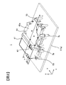
- FIG. 2 is an external perspective view of a power conversion device according to an embodiment of the present invention.
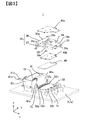
- FIG. 3 is an exploded perspective view of the power conversion device shown in FIG.
- FIG. 4 is a perspective view showing a connection structure between the capacitor of the power conversion device shown in FIG. 2 and the connection conductor.
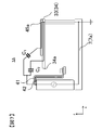
- FIG. 5 is a sectional view taken along line VV of the power conversion device shown in FIG.
- FIG. 6 is a schematic diagram showing the flow of EMC noise current in the power conversion device shown in FIG.
- FIG. 7 is a diagram showing a flow of EMC noise current of the power conversion device of the comparative example.
- FIG. 8 is a diagram showing a flow of EMC noise current of the power conversion device shown in FIG.
- FIG. 1 is a diagram showing an example of a circuit diagram of the power conversion device of the present invention.
- the power conversion device 1 includes an inverter main circuit 3 that converts DC power into AC power, a noise filter circuit unit 20 for suppressing electromagnetic noise generated when the inverter main circuit 3 performs power conversion operation, and a control unit 170. Be prepared.
- the power conversion device 1 illustrated in FIG. 1 includes a configuration surrounded by a frame including an inverter main circuit 3, a noise filter circuit unit 20, and a control unit 170.
- the inverter main circuit 3 is composed of a power conversion circuit unit 4 that converts DC power into AC power and a capacitor circuit unit 5 that smoothes DC power.
- the power conversion circuit unit 4 has three upper and lower arm series circuits 4a, 4b, and 4c.
- Each of the upper and lower arm series circuits 4a, 4b, and 4c includes a switching element 328 and a diode 156 such as an IGBT (insulated gate type bipolar transistor) that operates as an upper arm, and a switching element 330 and a diode 166 such as an IGBT that operates as a lower arm.
- the switching element 328 of the upper arm and the switching element 330 of the lower arm convert DC power into AC power.
- the diodes 156 and 166 also have a function of converting AC power into DC power during regeneration.
- the upper and lower arm series circuit 4a is connected to the u phase of the motor generator MG via the AC terminal 270a.
- the upper and lower arm series circuit 4b is connected to the v phase of the motor generator MG via the AC terminal 270a.
- the upper and lower arm series circuit 4c is connected to the w phase of the motor generator MG via the AC terminal 270a.
- the motor generator MG outputs the driving force of the HEV or EV based on the AC power supplied from the inverter main circuit 3 via the AC terminal 270a.
- the motor generator MG also acts as a generator that regenerates the AC power when the motor is rotated by an external force to the high voltage battery 2.
- the high voltage battery 2 is an HEV or an EV DC power source.
- the capacitor circuit unit 5 has a capacitor (capacitor) 51, is connected between the high voltage battery 2 and the power conversion circuit unit 4, smoothes the DC power, and supplies the DC power to the power conversion circuit unit 4.
- the noise filter circuit unit 20 is provided between the DC power supply terminal 6 and the capacitor circuit unit 5, and the power conversion circuit unit 4 suppresses electromagnetic noise generated during the power conversion operation.
- the noise filter circuit unit 20 includes a connecting conductor 10, an X capacitor 31, positive and negative Y capacitors 32p and 32n, and a core member 21.
- the connecting conductor 10 is a power transmission path that connects the high-voltage battery 2 and the capacitor circuit unit 5.
- the connecting conductor 10 includes a positive electrode side connecting conductor 10p and a negative electrode side connecting conductor 10n.
- the positive and negative electrode side connecting conductors 10p and 10n are connected to the positive and negative electrode side terminals of the high voltage battery 2 via the positive electrode side DC power supply terminal 6p and the negative electrode side DC power supply terminal 6n, respectively.
- the X capacitor 31 is provided between the positive electrode side connecting conductor 10p and the negative electrode side connecting conductor 10n, and smoothes power having a frequency higher than the power frequency smoothed by the capacitor circuit unit 5.
- the positive and negative electrode side Y capacitors 32p and 32n are provided between the positive electrode side connecting conductor 10p and the ground terminal 134, or between the negative electrode side connecting conductor 10n and the ground terminal 134, respectively, to smooth the electric power.
- the core member 21 suppresses electromagnetic noise by absorbing fluctuations in the current flowing through the connecting conductor 10.
- the positive electrode side terminal of the capacitor circuit unit 5 is connected to the collector of the switching element 328 of each upper arm and the cathode of the diode 156 by the positive electrode side connecting conductor 10p. Further, the negative electrode side terminal of the capacitor 51 is connected to the emitter of the switching element 330 of each lower arm and the anode of the diode 166 by the negative electrode side connecting conductor 10n.
- the control unit 170 includes a driver circuit 174 that drives and controls two power conversion circuit units 4, and a control circuit 172 that supplies a control signal to the driver circuit 174 via a signal line (bus line) 176.
- the gate terminals and emitter sense terminals of the IGBTs 328 and 330 of the upper and lower arm series circuits 4a, 4b, and 4c, respectively, are connected to the control unit 170.
- the upper and lower arm series circuits 4a, 4b, and 4c operate in response to the drive signal output from the control unit 170, and convert the DC power supplied from the high-voltage battery 2 into three-phase AC power. This converted power is supplied to the armature winding of the motor generator MG.
- the control circuit 172 includes a microcomputer for arithmetically processing the switching timings of the IGBTs 328 and 330.
- the target torque value required for the motor generator MG As input information to the microcomputer, the target torque value required for the motor generator MG, the current value supplied from the upper and lower arm series circuits 4a, 4b, and 4c to the armature winding of the motor generator MG, and the motor generator MG.
- the magnetic pole position of the rotor of is input.
- the target torque value is based on a command signal output from a higher-level control device (not shown).
- the current value is detected based on the detection signal output from the current sensor (not shown).
- the magnetic pole position is detected based on a detection signal output from a rotating magnetic pole sensor (not shown) provided in the motor generator MG.
- FIG. 2 is an external perspective view of a power conversion device according to an embodiment of the present invention.
- the power conversion device 1 has a housing formed by a case 7 and a cover (not shown).
- FIG. 2 shows a state in which the cover is removed from the case 7.
- the side wall for forming the storage portion is omitted, and only the bottom portion 7a of the storage portion is shown.
- the x-direction, y-direction, and z-direction are as shown in the figure.
- the case 7 is made of a metal such as an aluminum alloy.
- the case 7 is provided with a capacitor storage portion 53 at a substantially central portion in the width direction (y direction), and is separated from the capacitor storage portion 53 and has a base 33 on one side (right side in the drawing) in the longitudinal direction (x direction). Is placed.
- a plurality of capacitor elements 51a constituting the capacitor 51 are housed in the capacitor storage unit 53.
- a control circuit board 45a is arranged on the base 33, and is fixed to the base 33 by a fastening member 61 such as a screw.
- FIG. 3 is an exploded perspective view of the power conversion device shown in FIG. 2, and FIG. 4 is a perspective view showing a connection structure between the capacitor and the connecting conductor of the power conversion device shown in FIG.
- FIG. 5 is a sectional view taken along line VV of the power conversion device shown in FIG.
- the base 33 is made of a conductive metal such as an aluminum alloy, iron or copper.
- the base 33 has a substantially flat support portion 34, a conductive portion 35 extending in a direction substantially perpendicular to the xy surface of the support portion 34 (z direction), and the support portion 34 toward the bottom 7a side of the case 7. It has a plurality of mounting legs 38 that are extended.
- the control circuit board 45a is laminated above the support portion 34 of the base 33, and the control circuit board 45b is laminated below the support portion 34 of the base 33. That is, the control circuit board 45a and the control circuit board 45b are superposed on the support portion 34 of the base 33.
- the control circuit board 45a and the control circuit board 45b have the control circuit 172 shown in FIG.
- the conductive portion 35 extends in the stacking direction (z direction) of the support portion 34 of the base 33 and the control circuit boards 45a and 45b. As shown in FIG. 3, the conductive portion 35 is provided on both ends of the wide portion 35a extending in the y direction along one side side of the support portion 34 and the wide portion 35a. It has a pair of side portions 35b and 35c extending in the ⁇ x direction (capacitor 51 side) substantially at right angles to the surface.
- the conductive portion 35 has a first conductive portion 36 extending from the support portion 34 to the upper side (+ z direction) side and a second conductive portion 37 extending from the support portion 34 to the lower portion ( ⁇ z direction) side.
- the pair of side portions 35b and 35c are provided on both the first conductive portion 36 and the second conductive portion 37.
- a mounting hole 38a (see FIG. 3) is provided at the tip of each mounting leg 38.
- the base 33 is fixed to the boss portion 7b provided in the case 7 as shown in FIG. 2 by inserting a fastening member (not shown) such as a screw or a bolt into the mounting hole 38a of the mounting leg 38.
- a fastening member such as a screw or a bolt
- the semiconductor module 52 is arranged below the support portion 34 of the base 33, and is fixed to the fixing portion 7c provided on the bottom portion 7a of the case 7.
- the semiconductor module 52 has the upper and lower arm series circuits 4a, 4b, and 4c shown in FIG. As shown in FIG. 3, the semiconductor module 52 has a positive electrode DC terminal 52p, a negative electrode DC terminal 52n, and an AC terminal 52t, respectively, of the upper and lower arm series circuits 4a, 4b, and 4c.
- a drive circuit board 46 is arranged between the support portion 34 of the base 33 and the semiconductor module 52.
- the drive circuit board 46 has the driver circuit 174 shown in FIG.
- the positive electrode side bus bar 41 and the negative electrode side bus bar 42 connect the capacitor 51 and the semiconductor module 52 (see FIG. 3).
- the positive electrode side bus bar 41 and the negative electrode side bus bar 42 correspond to the positive electrode side connecting conductor 10p and the negative electrode side connecting conductor 10n shown in FIG. 1, respectively.
- the capacitor 51 and the base 33 form an EMC noise reduction structure described below.
- the positive electrode side bus bar 41 is connected to the positive electrode side DC power supply terminal 6p (see FIG. 1) of the DC power supply terminal 6 by the positive electrode terminal 41p on one end side, and the positive electrode terminal (shown) of the capacitor 51 at the connection portion 71 (see FIG. 5). It is connected to each positive electrode DC terminal 52p (see FIG. 3) of the semiconductor module 52 at the connection end 41c (see FIG. 4) on the other end side.
- the negative electrode side bus bar 42 is connected to the negative electrode side DC power supply terminal 6n (see FIG. 1) of the DC power supply terminal 6 by the negative electrode terminal 41n on one end side, and the negative electrode terminal (shown) of the capacitor 51 at the connection portion 72 (see FIG. 5).
- each negative electrode DC of the semiconductor module 52 is connected to the connection end portion 42c (see FIG. 4) on the other end side. It is connected to the terminal 52n (see FIG. 3). From the AC terminal 52t of the semiconductor module 52, the AC power obtained by the upper and lower arm series circuits 4a, 4b, and 4c is output.
- the positive and negative electrode side bus bars 41 and 42 are arranged apart from the conductive portion 35 of the base 33 in the longitudinal direction (x direction). Further, as shown in FIG. 2, the length of the positive / negative electrode side bus bars 41 and 42 in the width direction (y direction) is formed to be slightly shorter than the length between the pair of side portions 35b and 35c of the conductive portion 35. The positive and negative bus bars 41 and 42 are arranged apart from each of the side portions 35b and 35c of the conductive portion 35.
- a resin 43 (see FIG. 5) is interposed between the positive electrode side bus bar 41 and the negative electrode side bus bar 42, and the positive electrode side bus bar 41 and the negative electrode side bus bar 42 are insulated by the resin 43.
- the positive electrode side bus bar 41 and the negative electrode side bus bar 42 can be configured as a molded bus bar body integrated with the resin 43 by insert molding.
- the positive and negative side bus bars 41 and 42 have falling portions 41a and 42a, respectively.
- the falling portions 41a and 42a extend downward ( ⁇ z direction) side along the conductive portion 35 substantially parallel to the conductive portion 35 from the upper end 36a side of the first conductive portion 36.
- the positive and negative electrode side bus bars 41 and 42 are below the lower end 37a of the second conductive portion 37, and are fastening members such as screws and bolts to the positive and negative electrode DC terminals 52p and 52n of the semiconductor module 52, respectively (not shown). Is fixed by.
- the capacitor 51 is composed of a plurality of capacitor elements 51a.
- the plurality of capacitor elements 51a are electrically connected in parallel by the positive / negative electrode side terminals 71p and 72n of the positive / negative electrode side connecting portions 71 and 72 of the positive / negative electrode side bus bars 41 and 42.
- the positive electrode side bus bar 41 is illustrated as a structure arranged above the negative electrode side bus bar 42 (+ z direction), but the negative electrode side bus bar 42 is above the positive electrode side bus bar 41 (+ z direction).
- the structure may be arranged on the side.
- the upper end 36a of the first conductive portion 36 of the conductive portion 35 is above (+ z direction) the connecting portions 71 and 72 in which the positive and negative electrode side bus bars 41 and 42 are connected to the capacitor 51. It is extended to.
- control circuit board 45a is attached to the upper portion (+ z direction) side of the support portion 34 of the base 33.
- a control circuit board 45b is attached to the lower portion (-z direction) side of the support portion 34 of the base 33.
- the control circuit board 45a is arranged below the upper end 36a of the first conductive portion 36 of the conductive portion 35 (in the ⁇ z direction), in other words, on the support portion 34 side.
- the control circuit board 45b is arranged above the lower end 37a of the second conductive portion 37 of the conductive portion 35 (in the + z direction), in other words, on the support portion 34 side.
- the semiconductor module 52 has a metal case having good thermal conductivity such as an aluminum alloy.
- the metal case of the semiconductor module 52 has a pair of rectangular wide surfaces 52a and 52b and two pairs of narrow outer peripheral side surfaces provided between the peripheral portions of the wide surfaces 52a and 52b. It has 52c. That is, the outer peripheral side surface 52c is composed of four rectangular side surfaces.
- One wide surface 52a of the metal case of the semiconductor module 52 is thermally conductively coupled to, that is, thermally coupled to the fixing portion 7c provided on the bottom portion 7a of the case 7.
- the case 7 is formed with a cooling flow path through which a refrigerant such as cooling water flows, and the semiconductor module 52 is cooled via the fixing portion 7c of the case 7. Cooling fins may be formed on the wide surface 52a of the semiconductor module 52.
- the capacitor 51 is arranged on the left side ( ⁇ x direction) of the conductive portion 35 extending in the vertical direction (z direction).
- Control circuit boards 45a and 45b laminated on the support portion 34 of the base 33 are arranged on the right side (+ direction) of the conductive portion 35.
- the semiconductor module 52 is arranged in the region between the support portion 34 of the base 33 and the bottom portion 7a of the case 7.
- the semiconductor module 52 is arranged so that the wide surface 52a is in contact with the bottom portion 7a of the case 7 via the fixing portion 7c.
- the wide surface 52a of the metal case of the semiconductor module 52 has a large area in order to improve heat dissipation, if the wide surface 52a is arranged vertically to the bottom 7a of the case 7, the height of the power converter 1 will be increased. growing.
- the wide surface 52a of the semiconductor module 52 is arranged parallel to the bottom 7a of the case 7. As described above, by adopting the structure in which the semiconductor module 52 is arranged between the support portion 34 of the base 33 and the bottom portion 7a of the case 7, it is possible to reduce the height and size of the power conversion device 1.
- the drive circuit board 46 is arranged on the other wide surface 52b side of the semiconductor module 52.
- the drive circuit board 46 has a driver circuit 174 illustrated in FIG.
- the drive circuit board 46 is fixed on the upper end of the boss portion 7b (see FIG. 5) provided in the case 7.
- the drive circuit board 46 is connected to the control circuit board 45b by a connector 64 (see FIG. 5).
- the connector 64 corresponds to the bus line 176 illustrated in FIG.
- the positive / negative electrode side bus bars 41, 42 descend from the upper flat portions 41b, 42b along the conductive portion 35 substantially in parallel with the conductive portion 35, and are located slightly below the lower end 37a of the second conductive portion 37. In other words, it is connected to the semiconductor module 52 by bypassing the conductive portion 35.
- the support portion 34 of the base 33 has a substrate support surface (board installation surface) S f on which the support member 34s for supporting the control circuit board 45a is installed.
- the semiconductor module 52 is arranged on one side of the substrate supporting surface S f is an area overlapping the substrate supporting surface S f, connecting portions 71 and 72 which are connected to the capacitor 51 is positive, the negative bus bar 41, the substrate
- the semiconductor module 52 is arranged on the extension line of the support surface S f on the side opposite to the one side on which the semiconductor module 52 is arranged. That, z position of the connecting portion 71, 72 than the substrate supporting surface S f is a + z direction side.
- the first conductive portion 36 is provided so as to extend above (+ z direction) the connecting portions 71 and 72 of the positive and negative electrode side bus bars 41 and 42. As a result, the area where the positive and negative side bus bars 41 and 42 face the conductive portion 35 increases.
- FIG. 6 is a schematic diagram showing the flow of EMC noise current in the power conversion device shown in FIG.
- the base 33 has a support portion 34 provided with a support member 34s for supporting the control circuit board 45a.
- the base 33 is provided with a conductive portion 35 extending in the vertical direction (z direction) from the support portion 34.
- the capacitor 51 is arranged on the left ( ⁇ x direction) side of the conductive portion 35
- the control circuit board 45a is arranged on the right (+ x direction) side of the conductive portion 35.
- the falling portions 41a and 42a of the positive and negative side bus bars 41 and 42 are arranged on the left ( ⁇ x direction) side of the conductive portion 35. That is, the positive / negative electrode side bus bars 41 and 42 and the control circuit board 45a are separated by the conductive portion 35.
- EMC noise due to magnetic / capacitive coupling is generated between the positive / negative side bus bars 41 and 42 and the control circuit board 45a.
- EMC noise is dominated by capacitive coupling transmission.
- the positive / negative side bus bars 41 and 42 and the control circuit board 45a it extends in the vertical direction perpendicular to the xy plane, in other words, in the vertical direction which is the stacking direction of the base 33 and the control circuit board 45a.
- a conductive portion 35 is provided.
- Such members disposed due to the stray capacitance C 2 between the floating capacitance C 1 and a positive-negative electrode bus bar 41 and the conductive portion 35 between the positive and the negative bus bar 41, 42 and the control circuit board 45a Capacitive coupling occurs.
- the capacitive coupling due to the stray capacitance C 1 between the positive and the negative bus bar 41, 42 and the control circuit board 45a, EMC noise current, positive and negative electrode bus bar 41, 42 Flows from the control circuit board 45a to the grounding portion via the support portion 34 of the base 33 and the case 7.
- the capacitive coupling due to the stray capacitance C 2 between the positive and the negative bus bar 41, 42 and the conductive portion 35, EMC noise current from the positive-negative electrode bus bar 41, the conductive portion of the base 33 35 Flows to the grounding portion via the support portion 34 and the case 7.
- the conductive portion 35 extends in the vertical direction which is the stacking direction of the capacitor 51 and the control circuit board 45a, and the falling portions 41a and 42a of the positive and negative electrode side bus bars 41 and 42 are conductive portions. From the upper end 36a side of the 35 to the lower end 37a side, it extends along the conductive portion 35 substantially parallel to the conductive portion 35. Therefore, the facing area between the positive / negative electrode side bus bars 41, 42 and the conductive portion 35 is large, and therefore the stray capacitance C 2 between the positive / negative electrode side bus bars 41, 42 and the conductive portion 35 is large.
- the EMC noise current is shown as a diagram in which the EMC noise current flows from the side portion 33a of the base 33 opposite to the conductive portion 35 to the case 7.
- the base 33 has a plurality of mounting legs 38, and each mounting leg 38 is fixed to a boss portion 7b provided in the case 7 by a fastening member (not shown).
- the base 33 is fixed to the case 7 at a position close to the conductive portion 35. Therefore, the impedance of the path through which the EMC noise current flows becomes small, the EMC noise current shunted to the conductive portion 35 side becomes large, and the EMC noise reduction effect can be further enhanced.
- FIG. 7 is a schematic view showing the flow of the EMC noise current of the power conversion device 1A of the comparative example
- FIG. 8 is a schematic view showing the flow of the EMC noise current of the power conversion device 1 shown in FIG. ..
- the base 33 does not have the conductive portion 35. That is, the power conversion device 1A of the comparative example does not have the conductive portion 35 extending in the vertical direction (z direction) between the support portion 34 of the base 33 and the positive / negative electrode side bus bars 41 and 42.
- Positive / negative electrode side bus bars 41, 42 are arranged directly facing the end portion 34a of the support portion 34 of the base 33 and the control circuit board 45a.
- the stray capacitance between the positive and the negative bus bar 41 and the base 33 C 2 is connected in parallel.
- EMC noise currents from noise source to the floating capacitance C 1, C 2 is shunted by stray capacitance C 1, the ratio of C 2 arranged in parallel.
- the stray capacitance C 1 and the stray capacitance C 2 are substantially equal. That is, C 1 ⁇ C 2 . Therefore, the EMC noise currents I 1 and I 2 passing through the stray capacitances C 1 and C 2 are I 1 ⁇ I 2 .
- the first conductor extending in the vertical direction between the support portion 34 of the base 33 and the positive / negative electrode side bus bars 41 and 42.
- a portion 36 is provided.
- the positive and negative electrode side bus bars 41 and 42 extend in the vertical direction along the first conductive portion 36.
- the control circuit board 45a is arranged at a position farther from the positive / negative electrode side bus bars 41 and 42 than the first conductive portion 36. Therefore, the relationship between the stray capacitance C1 and the stray capacitance C2 is C 2 >> C 1 . Therefore, the EMC noise currents I 1 and I 2 passing through the stray capacitances C 1 and C 2 are I 2 >> I 1 .
- the EMC noise current from the positive / negative side bus bars 41 and 42 which are noise sources, is overwhelmingly distributed to the conductive portion 35 as compared with the control circuit board 45a. Therefore, the EMC noise current flowing from the positive / negative side bus bars 41 and 42 to the control circuit board 45a can be significantly reduced.
- a second conductive portion 37 is provided between the positive / negative electrode side bus bars 41 and 42 and the control circuit board 45b.
- the control circuit board 45b is arranged above (+ z direction) side from the lower end 37a of the second conductive portion 37 in the vertical direction. Therefore, the stray capacitance between the positive / negative electrode side bus bars 41 and 42 and the control circuit board 45b is smaller than the stray capacitance C 2 between the positive / negative electrode side bus bars 41 and 42 and the conductive portion 35. Therefore, the EMC noise current flowing from the positive / negative side bus bars 41 and 42 to the control circuit board 45b is smaller than the positive / negative side bus bars 41 and 42 flowing from the positive / negative side bus bars 41 and 42 to the base 33.
- the conductive portion 35 has a second conductive portion 37 extending to the drive circuit board 46 side having the drive circuit for driving the semiconductor module 52. Therefore, the stray capacitance C between the positive / negative electrode side bus bars 41, 42 and the second conductive portion 37 becomes larger than the stray capacitance between the positive / negative electrode side bus bars 41, 42 and the drive circuit board 46, and the drive circuit board 46 is driven. The EMC noise current flowing through the circuit board 46 is reduced.
- the conductive portion 35 is exemplified as a structure extending in the direction perpendicular to the xy plane.
- the conductive portion 35 may have a structure that is inclined with respect to the xy plane.
- the positive / negative electrode side bus bars 41 and 42 extend in parallel along the conductive portion 35 in order to increase the stray capacitance with the conductive portion 35. Is preferable.
- the power conversion device 1 controls the semiconductor module 52 having the power conversion circuit unit 4, the capacitor 51 that smoothes the DC power and supplies it to the power conversion circuit unit, and the power conversion circuit unit 4.
- the control circuit board 45a having a circuit and arranged apart from the capacitor 51, the positive / negative side bus bars (connection conductors) 41 and 42 connecting the semiconductor module 52 and the capacitor 51, and the control circuit board 45a are grounded.
- the base 33 is electrically connected to the unit and the control circuit board 45a is laminated, and the conductive portion 35 is electrically connected to the base 33 and extends in the stacking direction of the base 33 and the control circuit board 45a.
- the positive / negative side bus bars 41 and 42 are connected to the semiconductor module by bypassing the conductive portion 35. Therefore, positive and negative electrode stray capacitance C 1 between the bus bars 41, 42 and the control circuit board 45 can be smaller than the stray capacitance C 2 between the positive and the negative bus bar 41, 42 and the conductive portion 35 , The EMC noise current flowing through the control circuit board 45a can be reduced.
- the conductive portion 35 and the base 33 are integrally molded. Therefore, the conductive portion 35 and the base 33 can be efficiently produced by casting or the like.
- the conductive portion 35 extends substantially parallel to the stacking direction of the base 33 and the control circuit board 45a. Therefore, the facing area between the conductive portion 35 and the positive / negative electrode side bus bars 41 and 42 can be increased, and the stray capacitance between the conductive portion 35 and the positive and negative electrode side bus bars 41 and 42 can be increased to increase the stray capacitance of the control circuit board.
- the EMC noise current flowing through 45a can be reduced.
- the base 33 has a support portion 34 on which the control circuit board 45a is laminated, the control circuit board 45a is arranged on one side of the support portion 34 in the stacking direction, and the semiconductor module 52 is laminated with the support portion 34. It is located on the other side of the direction. Since the structure is such that the semiconductor module 52 is arranged without the space region on the opposite side of the control circuit board 45a of the support portion 34, the height and size of the power conversion device 1 can be reduced.
- the base 33 has a substrate supporting surface S f for supporting the control circuit board 45a, the semiconductor module 52, one side in the stacking direction in which the base 33 and the control circuit board 45a of the substrate supporting surface S f are laminated disposed, connecting portions 71 and 72 which are connected to the capacitor 51 is positive, the negative bus bar 41, 42 is arranged on the other side of the substrate supporting surface S f in the extension of the substrate support surface S f. Therefore, stray capacitance C 1 becomes smaller between the positive and negative electrode bus bar 41 and the control circuit board 45a, the reduction of EMC noise current flowing through the control circuit board 45a becomes more effective.
- the base 33 has a substrate supporting surface S f for supporting the control circuit board 45a, a distance L1 from the substrate supporting surface S f of the upper end 36a of the base 33, the positive-negative electrode bus bar 41 and a capacitor greater than the distance L2 from the extension line of the substrate supporting surface S f of the connecting portions 71 and 72 which are connected to 51. Therefore, the facing area between the positive / negative electrode side bus bars 41, 42 and the conductive portion 35 becomes large, the stray capacitance C 2 between the positive / negative electrode side bus bars 41, 42 and the conductive portion 35 becomes large, and the control circuit board The reduction of the EMC noise current flowing through 45a becomes more effective.
- the control circuit board 45a includes a control circuit board 45a arranged on one side of the base 33 and a control circuit board 45b arranged on the opposite side facing the one side, and the base 33 includes the control circuit board 45a and the control circuit board 45a. It has a support portion 34 that supports the control circuit board 45b, and the conductive portion 35 extends from the support portion 34 to the control circuit board 45a side and a first conductive portion 36 extending from the support portion 34 to the control circuit board 45b side.
- the existing second conductive portion 37 is included.
- the stray capacitance C between the positive and negative side bus bars 41 and 42 and each of the first conductive portion 36 and the second conductive portion 37 is different from the positive and negative side bus bars 41 and 42) with the control circuit boards 45a and 45b. It becomes larger than the stray capacitance between them, and the EMC noise current flowing through the control circuit boards 45a and 45b is reduced.
- a drive circuit board 46 having a drive circuit for driving the semiconductor module 52 is further provided, and the conductive portion 35 has a second conductive portion 37 extending to the drive circuit board 46 side. Therefore, the stray capacitance C between the positive / negative electrode side bus bars 41, 42 and the conductive portion 35 becomes larger than the stray capacitance between the positive / negative electrode side bus bars 41, 42 and the drive circuit board 46, and the drive circuit board 46 The EMC noise current flowing through the circuit board is reduced.
- a case 7 having a bottom (one surface) 7a substantially parallel to the control circuit board 45a is provided, and the semiconductor module 52 includes a pair of wide surfaces 52a and 52b and a narrow outer peripheral side surface 52c surrounding the outer periphery of the wide surface 52a.
- the wide surface 52a of the semiconductor module 52 and the bottom portion 7a substantially parallel to the control circuit board 45a of the case 7 are thermally coupled to each other.
- a wide surface 52a having a large area of the semiconductor module 52 is arranged substantially parallel to the bottom 7a of the control circuit board 45a, and the semiconductor module 52 is arranged in a direction orthogonal to the control circuit board 45a by thermally coupling to the bottom 7a. It is possible to reduce the height of the power conversion device 1 from the structure, and it is possible to obtain a low-profile power conversion device 1 capable of cooling the semiconductor module 52.
- control circuit boards 45a and 45b are provided on the upper and lower surfaces of the base 33, respectively.
- control circuit board 45a (45b) may be provided only on the upper surface or the lower surface of the base 33.
- the base 33 has a first conductive portion 36 extending upward (+ z direction) side of the support portion 34 and a second conductive portion extending downward ( ⁇ z direction) side of the support portion 34. Illustrated as a structure having 37. However, if the control circuit boards 45a and 45b are arranged only on one surface side of the support portion 34, the conductive portion 35 (36) extends only on the side where the control circuit boards 45a and 45b are arranged in the base 33. It can be an existing structure.
- the base 33 in which the first conductive portion 36 and the second conductive portion 37 are integrally molded by casting or the like is exemplified.
- the first conductive portion 36 and / or the second conductive portion 37 may be formed as a separate member from the base 33 and fixed to the base 33.
- the conductive portion 35 may have a structure integrally molded with the case 7.
- the structure may be such that the conductive portion is connected to a side wall (not shown) provided in the case 7.
- one of the pair of wide surfaces 52a and 52b of the semiconductor module 52 is thermally coupled to the bottom portion 7a of the case 7 to be cooled.
- both of the pair of wide surfaces 52a and 52b of the semiconductor module 52 may be cooled.
- Power conversion device 4 Power conversion circuit part 7 Case 7a Bottom 10 Connecting conductor 33 Base 34 Support part 35 Conductive part 35a, 35b Wide part 36 1st conductive part 36a Upper end 37 2nd conductive part 37a Lower end 41 Positive electrode side bus bar (connecting conductor) ) 42 Negative electrode side bus bar (connecting conductor) 45a, 45b Control circuit board 46 Drive circuit board 51 Capacitor 52 Semiconductor module 52a, 52b Wide surface 71, 72 Connection part 72 Connection part 170 Control part 172 Control circuit S f board support surface L1, L2 distance
Abstract
The present invention provides a power conversion device in which an EMC noise current flowing through a control circuit board is reduced. The power control device 1 is provided with: a semiconductor module 52; a capacitor 51; a control circuit board 45a; positive/negative-electrode-side busbars 41, 42 for connecting the semiconductor module 52 and the capacitor 51; a base 33 electrically connected to a ground part of the control circuit board 45a, the control circuit board 45a being stacked on the base 33; and an electroconductive part 35 electrically connected to the base 33, the electroconductive part 35 extending in the direction in which the base 33 and the control circuit board 45a are stacked. The positive/negative-electrode-side busbars 41, 42 are connected to the semiconductor module 52 so as to bypass the electroconductive part 53.
Description
本発明は、電力変換装置に関する。
The present invention relates to a power conversion device.
ハイブリッド車やプラグインハイブリッド車、電気自動車などの車両には、モータ駆動用のインバータ、商用電源から高電圧バッテリに充電する充電器、および補機バッテリに給電するDCDCコンバータ等、種々の電力変換装置が搭載されている。モータ駆動用のインバータ等の電力変換装置は、金属ケース内に、直流電力を平滑化するコンデンサと、直流電力を交流電力に変換する電力変換回路部を有する半導体モジュールと、コンデンサとパワーモジュールとを直流電源に接続するバスバーとが収納された構造を有する。
For vehicles such as hybrid vehicles, plug-in hybrid vehicles, and electric vehicles, various power conversion devices such as inverters for driving motors, chargers for charging high-voltage batteries from commercial power sources, and DCDC converters for supplying power to auxiliary batteries Is installed. A power conversion device such as an inverter for driving a motor includes a capacitor for smoothing DC power, a semiconductor module having a power conversion circuit for converting DC power to AC power, and a capacitor and a power module in a metal case. It has a structure in which a bus bar connected to a DC power supply is housed.
このような電力変換装置の一例として、パワーモジュールの上方に制御回路基板を配し、コンデンサをパワーモジュールの側方に配し、直流電源に接続される正極側バスバーおよび負極側バスバーによりコンデンサとパワーモジュールとを接続した構造が知られている。正・負極側バスバーは樹脂により一体化されており、それぞれ、パワーモジュールの正極側端子または負極側端子に接続されている。正・負極側バスバーとパワーモジュールの正・負極側端子との接続部は、制御回路基板に近接する位置で、直接、制御回路基板に対向して配置されている(例えば、特許文献1の図2等参照)。
As an example of such a power conversion device, a control circuit board is arranged above the power module, a capacitor is arranged on the side of the power module, and a capacitor and power are provided by a positive electrode side bus bar and a negative electrode side bus bar connected to a DC power supply. The structure connected to the module is known. The positive and negative bus bars are integrated with resin and are connected to the positive electrode side terminal or the negative electrode side terminal of the power module, respectively. The connection portion between the positive / negative electrode side bus bar and the positive / negative electrode side terminal of the power module is arranged at a position close to the control circuit board and directly facing the control circuit board (for example, the figure of Patent Document 1). See 2nd class).
特許文献1のように、強電系回路部であるコンデンサ回路部と弱電系回路部である制御回路とが近接して配置された構造を有する電力変換装置では、制御回路基板を流れるEMC(Electromagnetic Compatibility)ノイズ電流が大きくなり、制御回路が誤動作する対策が施されるが、更なる改善が要求されている。
As in Patent Document 1, in a power conversion device having a structure in which a capacitor circuit portion which is a strong electric system circuit portion and a control circuit which is a weak electric system circuit portion are arranged close to each other, EMC (Electromagnetic Compatibility) flowing through a control circuit board is used. ) Measures are taken to increase the noise current and cause the control circuit to malfunction, but further improvement is required.
本発明の一態様によると、電力変換装置は、電力変換回路部を有する半導体モジュールと、直流電力を平滑化して前記電力変換回路部に供給するキャパシタと、前記電力変換回路部を制御する制御回路を有し、前記キャパシタと離間して配置された制御回路基板と、前記半導体モジュールと前記キャパシタとを接続する接続導体と、前記制御回路基板の接地部に電気的に接続され、前記制御回路基板が積層されるベースと、前記ベースに電気的に接続され、前記ベースと前記制御回路基板の積層方向に延在された導電部とを備え、前記接続導体は、前記導電部を迂回して前記半導体モジュールに接続されている。
According to one aspect of the present invention, the power conversion device includes a semiconductor module having a power conversion circuit unit, a capacitor that smoothes DC power and supplies it to the power conversion circuit unit, and a control circuit that controls the power conversion circuit unit. The control circuit board is electrically connected to the grounding portion of the control circuit board, the control circuit board arranged apart from the capacitor, the connecting conductor connecting the semiconductor module and the capacitor, and the control circuit board. The base is electrically connected to the base and has a conductive portion extending in the stacking direction of the base and the control circuit board, and the connecting conductor bypasses the conductive portion. It is connected to a semiconductor module.
本発明によれば、正・負極側バスバーと制御回路基板間の浮遊容量を低減して、制御回路基板を流れるEMC(Electromagnetic Compatibility)ノイズ電流を低減することができる。
According to the present invention, it is possible to reduce the stray capacitance between the positive / negative side bus bars and the control circuit board, and reduce the EMC (Electromagnetic Compatibility) noise current flowing through the control circuit board.
以下、図面を参照して本発明の電力変換装置の一実施の形態を説明する。
図1は、本発明の電力変換装置の回路図の一例を示す図である。
電力変換装置1は、直流電力を交流電力に変換するインバータ主回路3と、インバータ主回路3が電力変換動作時に発生する電磁ノイズを抑制するためのノイズフィルタ回路部20と、制御部170とを備える。図1に図示される電力変換装置1は、インバータ主回路3と、ノイズフィルタ回路部20と、制御部170とを含む枠で囲まれた構成を備える。 Hereinafter, an embodiment of the power conversion device of the present invention will be described with reference to the drawings.
FIG. 1 is a diagram showing an example of a circuit diagram of the power conversion device of the present invention.
Thepower conversion device 1 includes an inverter main circuit 3 that converts DC power into AC power, a noise filter circuit unit 20 for suppressing electromagnetic noise generated when the inverter main circuit 3 performs power conversion operation, and a control unit 170. Be prepared. The power conversion device 1 illustrated in FIG. 1 includes a configuration surrounded by a frame including an inverter main circuit 3, a noise filter circuit unit 20, and a control unit 170.
図1は、本発明の電力変換装置の回路図の一例を示す図である。
電力変換装置1は、直流電力を交流電力に変換するインバータ主回路3と、インバータ主回路3が電力変換動作時に発生する電磁ノイズを抑制するためのノイズフィルタ回路部20と、制御部170とを備える。図1に図示される電力変換装置1は、インバータ主回路3と、ノイズフィルタ回路部20と、制御部170とを含む枠で囲まれた構成を備える。 Hereinafter, an embodiment of the power conversion device of the present invention will be described with reference to the drawings.
FIG. 1 is a diagram showing an example of a circuit diagram of the power conversion device of the present invention.
The
インバータ主回路3は、直流電力を交流電力に変換する電力変換回路部4と、直流電力を平滑化するコンデンサ回路部5とにより構成される。
電力変換回路部4は、3つの上下アーム直列回路4a、4b、4cを有する。各上下アーム直列回路4a、4b、4cは、上アームとして動作するIGBT(絶縁ゲート型バイポーラトランジスタ)等のスイッチング素子328およびダイオード156と、下アームとして動作するIGBT等のスイッチング素子330およびダイオード166とを有する。上アームのスイッチング素子328と下アームのスイッチング素子330は、直流電力を交流電力に変換する。ダイオード156、166は、回生時には交流電力を直流電力に変換する機能も有する。 The invertermain circuit 3 is composed of a power conversion circuit unit 4 that converts DC power into AC power and a capacitor circuit unit 5 that smoothes DC power.
The power conversion circuit unit 4 has three upper and lower arm series circuits 4a, 4b, and 4c. Each of the upper and lower arm series circuits 4a, 4b, and 4c includes a switching element 328 and a diode 156 such as an IGBT (insulated gate type bipolar transistor) that operates as an upper arm, and a switching element 330 and a diode 166 such as an IGBT that operates as a lower arm. Has. The switching element 328 of the upper arm and the switching element 330 of the lower arm convert DC power into AC power. The diodes 156 and 166 also have a function of converting AC power into DC power during regeneration.
電力変換回路部4は、3つの上下アーム直列回路4a、4b、4cを有する。各上下アーム直列回路4a、4b、4cは、上アームとして動作するIGBT(絶縁ゲート型バイポーラトランジスタ)等のスイッチング素子328およびダイオード156と、下アームとして動作するIGBT等のスイッチング素子330およびダイオード166とを有する。上アームのスイッチング素子328と下アームのスイッチング素子330は、直流電力を交流電力に変換する。ダイオード156、166は、回生時には交流電力を直流電力に変換する機能も有する。 The inverter
The power conversion circuit unit 4 has three upper and lower
上下アーム直列回路4aは、交流ターミナル270aを介してモータジェネレータMGのu相と接続される。上下アーム直列回路4bは、交流ターミナル270aを介してモータジェネレータMGのv相と接続される。上下アーム直列回路4cは、交流ターミナル270aを介してモータジェネレータMGのw相と接続される。
The upper and lower arm series circuit 4a is connected to the u phase of the motor generator MG via the AC terminal 270a. The upper and lower arm series circuit 4b is connected to the v phase of the motor generator MG via the AC terminal 270a. The upper and lower arm series circuit 4c is connected to the w phase of the motor generator MG via the AC terminal 270a.
モータジェネレータMGは、交流ターミナル270aを介してインバータ主回路3から供給される交流電力に基づいてHEVまたはEVの駆動力を出力する。また、モータジェネレータMGは外力でモータが回転した際の交流電力を高電圧バッテリ2へ回生するジェネレータとしても作用する。高電圧バッテリ2は、HEVまたはEVの直流電源である。
The motor generator MG outputs the driving force of the HEV or EV based on the AC power supplied from the inverter main circuit 3 via the AC terminal 270a. The motor generator MG also acts as a generator that regenerates the AC power when the motor is rotated by an external force to the high voltage battery 2. The high voltage battery 2 is an HEV or an EV DC power source.
コンデンサ回路部5は、コンデンサ(キャパシタ)51を有し、高電圧バッテリ2と電力変換回路部4との間に接続され、直流電力を平滑化し電力変換回路部4に供給する。
The capacitor circuit unit 5 has a capacitor (capacitor) 51, is connected between the high voltage battery 2 and the power conversion circuit unit 4, smoothes the DC power, and supplies the DC power to the power conversion circuit unit 4.
ノイズフィルタ回路部20は、直流電源端子6とコンデンサ回路部5との間に設けられ、電力変換回路部4が電力変換動作時に発生する電磁ノイズを抑制する。
ノイズフィルタ回路部20は、接続導体10と、Xコンデンサ31と、正・負極側Yコンデンサ32p、32nと、コア部材21とを有する。接続導体10は、高電圧バッテリ2とコンデンサ回路部5との間を接続する電力伝送経路である。接続導体10は、正極側接続導体10pと、負極側接続導体10nとを含む。正・負極側接続導体10p、10nは、それぞれ、正極側直流電源端子6p、負極側直流電源端子6nを介して高電圧バッテリ2の正・負極側端子に接続される。 The noisefilter circuit unit 20 is provided between the DC power supply terminal 6 and the capacitor circuit unit 5, and the power conversion circuit unit 4 suppresses electromagnetic noise generated during the power conversion operation.
The noisefilter circuit unit 20 includes a connecting conductor 10, an X capacitor 31, positive and negative Y capacitors 32p and 32n, and a core member 21. The connecting conductor 10 is a power transmission path that connects the high-voltage battery 2 and the capacitor circuit unit 5. The connecting conductor 10 includes a positive electrode side connecting conductor 10p and a negative electrode side connecting conductor 10n. The positive and negative electrode side connecting conductors 10p and 10n are connected to the positive and negative electrode side terminals of the high voltage battery 2 via the positive electrode side DC power supply terminal 6p and the negative electrode side DC power supply terminal 6n, respectively.
ノイズフィルタ回路部20は、接続導体10と、Xコンデンサ31と、正・負極側Yコンデンサ32p、32nと、コア部材21とを有する。接続導体10は、高電圧バッテリ2とコンデンサ回路部5との間を接続する電力伝送経路である。接続導体10は、正極側接続導体10pと、負極側接続導体10nとを含む。正・負極側接続導体10p、10nは、それぞれ、正極側直流電源端子6p、負極側直流電源端子6nを介して高電圧バッテリ2の正・負極側端子に接続される。 The noise
The noise
Xコンデンサ31は、正極側接続導体10pと負極側接続導体10nの間に設けられ、コンデンサ回路部5が平滑化する電力の周波数より高い周波数の電力を平滑化する。正・負極側Yコンデンサ32p、32nは、それぞれ、正極側接続導体10pとグランド端子134の間、または負極側接続導体10nとグランド端子134の間に設けられ、電力を平滑化する。
コア部材21は、接続導体10に流れる電流の変動を吸収することで電磁ノイズを抑制する。 TheX capacitor 31 is provided between the positive electrode side connecting conductor 10p and the negative electrode side connecting conductor 10n, and smoothes power having a frequency higher than the power frequency smoothed by the capacitor circuit unit 5. The positive and negative electrode side Y capacitors 32p and 32n are provided between the positive electrode side connecting conductor 10p and the ground terminal 134, or between the negative electrode side connecting conductor 10n and the ground terminal 134, respectively, to smooth the electric power.
Thecore member 21 suppresses electromagnetic noise by absorbing fluctuations in the current flowing through the connecting conductor 10.
コア部材21は、接続導体10に流れる電流の変動を吸収することで電磁ノイズを抑制する。 The
The
コンデンサ回路部5の正極側端子は、正極側接続導体10pにより、各上アームのスイッチング素子328のコレクタおよびダイオード156のカソードに接続される。また、コンデンサ51の負極側端子は、負極側接続導体10nにより、各下アームのスイッチング素子330のエミッタおよびダイオード166のアノードに接続される。
The positive electrode side terminal of the capacitor circuit unit 5 is connected to the collector of the switching element 328 of each upper arm and the cathode of the diode 156 by the positive electrode side connecting conductor 10p. Further, the negative electrode side terminal of the capacitor 51 is connected to the emitter of the switching element 330 of each lower arm and the anode of the diode 166 by the negative electrode side connecting conductor 10n.
制御部170は、2つの電力変換回路部4を駆動制御するドライバ回路174と、ドライバ回路174へ信号線(バスライン)176を介して制御信号を供給する制御回路172とを含む。上下アーム直列回路4a、4b、4cそれぞれのIGBT328、330のゲート端子およびエミッタセンス端子は、制御部170に接続されている。上下アーム直列回路4a、4b、4cは、制御部170から出力された駆動信号を受けて動作し、高電圧バッテリ2から供給された直流電力を三相交流電力に変換する。この変換された電力は、モータジェネレータMGの電機子巻線に供給される。
The control unit 170 includes a driver circuit 174 that drives and controls two power conversion circuit units 4, and a control circuit 172 that supplies a control signal to the driver circuit 174 via a signal line (bus line) 176. The gate terminals and emitter sense terminals of the IGBTs 328 and 330 of the upper and lower arm series circuits 4a, 4b, and 4c, respectively, are connected to the control unit 170. The upper and lower arm series circuits 4a, 4b, and 4c operate in response to the drive signal output from the control unit 170, and convert the DC power supplied from the high-voltage battery 2 into three-phase AC power. This converted power is supplied to the armature winding of the motor generator MG.
制御回路172は、IGBT328、330のスイッチングタイミングを演算処理するためのマイクロコンピュータを備えている。マイクロコンピュータには入力情報として、モータジェネレータMGに対して要求される目標トルク値、上下アーム直列回路4a、4b、4cからモータジェネレータMGの電機子巻線に供給される電流値、及びモータジェネレータMGの回転子の磁極位置が入力されている。目標トルク値は、不図示の上位の制御装置から出力された指令信号に基づくものである。電流値は、電流センサ(不図示)から出力された検出信号に基づいて検出されたものである。磁極位置は、モータジェネレータMGに設けられた回転磁極センサ(不図示)から出力された検出信号に基づいて検出されたものである。
The control circuit 172 includes a microcomputer for arithmetically processing the switching timings of the IGBTs 328 and 330. As input information to the microcomputer, the target torque value required for the motor generator MG, the current value supplied from the upper and lower arm series circuits 4a, 4b, and 4c to the armature winding of the motor generator MG, and the motor generator MG. The magnetic pole position of the rotor of is input. The target torque value is based on a command signal output from a higher-level control device (not shown). The current value is detected based on the detection signal output from the current sensor (not shown). The magnetic pole position is detected based on a detection signal output from a rotating magnetic pole sensor (not shown) provided in the motor generator MG.
図2は、本発明の一実施の形態としての電力変換装置の外観斜視図である。
電力変換装置1は、ケース7と、不図示のカバーとにより形成される筐体を有する。
図2は、カバーがケース7から取り外された状態が示されている。ケース7は、収納部を形成するための側壁が省略され、収納部の底部7aのみが図示されている。
なお、以下の説明において、x方向、y方向、z方向は図示の通りとする。 FIG. 2 is an external perspective view of a power conversion device according to an embodiment of the present invention.
Thepower conversion device 1 has a housing formed by a case 7 and a cover (not shown).
FIG. 2 shows a state in which the cover is removed from thecase 7. In the case 7, the side wall for forming the storage portion is omitted, and only the bottom portion 7a of the storage portion is shown.
In the following description, the x-direction, y-direction, and z-direction are as shown in the figure.
電力変換装置1は、ケース7と、不図示のカバーとにより形成される筐体を有する。
図2は、カバーがケース7から取り外された状態が示されている。ケース7は、収納部を形成するための側壁が省略され、収納部の底部7aのみが図示されている。
なお、以下の説明において、x方向、y方向、z方向は図示の通りとする。 FIG. 2 is an external perspective view of a power conversion device according to an embodiment of the present invention.
The
FIG. 2 shows a state in which the cover is removed from the
In the following description, the x-direction, y-direction, and z-direction are as shown in the figure.
ケース7は、アルミニウム合金等の金属により形成されている。
ケース7には、幅方向(y方向)のほぼ中央部にコンデンサ収納部53が設けられており、コンデンサ収納部53から離間して長手方向(x方向)の一方側(図示右側)にベース33が配置されている。詳細は後述するが、コンデンサ収納部53内にはコンデンサ51を構成する複数のコンデンサ素子51a(図4参照)が収納されている。ベース33上には、制御回路基板45aが配置され、ねじ等の締結部材61によりベース33に固定されている。 Thecase 7 is made of a metal such as an aluminum alloy.
Thecase 7 is provided with a capacitor storage portion 53 at a substantially central portion in the width direction (y direction), and is separated from the capacitor storage portion 53 and has a base 33 on one side (right side in the drawing) in the longitudinal direction (x direction). Is placed. Although the details will be described later, a plurality of capacitor elements 51a (see FIG. 4) constituting the capacitor 51 are housed in the capacitor storage unit 53. A control circuit board 45a is arranged on the base 33, and is fixed to the base 33 by a fastening member 61 such as a screw.
ケース7には、幅方向(y方向)のほぼ中央部にコンデンサ収納部53が設けられており、コンデンサ収納部53から離間して長手方向(x方向)の一方側(図示右側)にベース33が配置されている。詳細は後述するが、コンデンサ収納部53内にはコンデンサ51を構成する複数のコンデンサ素子51a(図4参照)が収納されている。ベース33上には、制御回路基板45aが配置され、ねじ等の締結部材61によりベース33に固定されている。 The
The
図3は、図2に図示された電力変換装置の分解斜視図であり、図4は、図2に図示された電力変換装置のコンデンサと接続導体との接続構造を示す斜視図である。図5は、図2に図示された電力変換装置のV-V線断面図である。
ベース33は、アルミニウム合金、鉄または銅などの導電性金属により形成されている。ベース33は、ほぼ平坦な支持部34と、支持部34のxy面に対しほぼ直角方向(z方向)に延在された導電部35と、支持部34からケース7の底部7a側に向けて延在された複数の取付脚38とを有する。
ベース33の支持部34の上方には制御回路基板45aが積層され、ベース33の支持部34の下方には制御回路基板45bが積層されている。つまり、制御回路基板45aおよび制御回路基板45bは、ベース33の支持部34に重ね合わされている。制御回路基板45aおよび制御回路基板45bは、図1に示す制御回路172を有している。 FIG. 3 is an exploded perspective view of the power conversion device shown in FIG. 2, and FIG. 4 is a perspective view showing a connection structure between the capacitor and the connecting conductor of the power conversion device shown in FIG. FIG. 5 is a sectional view taken along line VV of the power conversion device shown in FIG.
Thebase 33 is made of a conductive metal such as an aluminum alloy, iron or copper. The base 33 has a substantially flat support portion 34, a conductive portion 35 extending in a direction substantially perpendicular to the xy surface of the support portion 34 (z direction), and the support portion 34 toward the bottom 7a side of the case 7. It has a plurality of mounting legs 38 that are extended.
Thecontrol circuit board 45a is laminated above the support portion 34 of the base 33, and the control circuit board 45b is laminated below the support portion 34 of the base 33. That is, the control circuit board 45a and the control circuit board 45b are superposed on the support portion 34 of the base 33. The control circuit board 45a and the control circuit board 45b have the control circuit 172 shown in FIG.
ベース33は、アルミニウム合金、鉄または銅などの導電性金属により形成されている。ベース33は、ほぼ平坦な支持部34と、支持部34のxy面に対しほぼ直角方向(z方向)に延在された導電部35と、支持部34からケース7の底部7a側に向けて延在された複数の取付脚38とを有する。
ベース33の支持部34の上方には制御回路基板45aが積層され、ベース33の支持部34の下方には制御回路基板45bが積層されている。つまり、制御回路基板45aおよび制御回路基板45bは、ベース33の支持部34に重ね合わされている。制御回路基板45aおよび制御回路基板45bは、図1に示す制御回路172を有している。 FIG. 3 is an exploded perspective view of the power conversion device shown in FIG. 2, and FIG. 4 is a perspective view showing a connection structure between the capacitor and the connecting conductor of the power conversion device shown in FIG. FIG. 5 is a sectional view taken along line VV of the power conversion device shown in FIG.
The
The
図5に図示されるように、導電部35は、ベース33の支持部34と制御回路基板45a、45bの積層方向(z方向)に延在されている。導電部35は、図3に図示されるように、支持部34の一側辺に沿ってy方向に長く延出された幅広部35aと、幅広部35aの両端に設けられ、幅広部35aに対しほぼ直角に-x方向(コンデンサ51側)に延在された一対の側部35b、35cを有する。導電部35は、支持部34から上部(+z方向)側に延在する第1導電部36と、支持部34から下部(-z方向)側に延在する第2導電部37を有する。一対の側部35b、35cは、第1導電部36および第2導電部37の両方に設けられている。
As shown in FIG. 5, the conductive portion 35 extends in the stacking direction (z direction) of the support portion 34 of the base 33 and the control circuit boards 45a and 45b. As shown in FIG. 3, the conductive portion 35 is provided on both ends of the wide portion 35a extending in the y direction along one side side of the support portion 34 and the wide portion 35a. It has a pair of side portions 35b and 35c extending in the −x direction (capacitor 51 side) substantially at right angles to the surface. The conductive portion 35 has a first conductive portion 36 extending from the support portion 34 to the upper side (+ z direction) side and a second conductive portion 37 extending from the support portion 34 to the lower portion (−z direction) side. The pair of side portions 35b and 35c are provided on both the first conductive portion 36 and the second conductive portion 37.
各取付脚38の先端部には取付孔38a(図3参照)が設けられている。ベース33は、取付脚38の取付孔38aにねじ、ボルト等の締結部材(図示せず)を挿通して、図2に図示されるように、ケース7に設けられたボス部7bに固定される。
A mounting hole 38a (see FIG. 3) is provided at the tip of each mounting leg 38. The base 33 is fixed to the boss portion 7b provided in the case 7 as shown in FIG. 2 by inserting a fastening member (not shown) such as a screw or a bolt into the mounting hole 38a of the mounting leg 38. To.
半導体モジュール52は、ベース33の支持部34の下方に配置され、ケース7の底部7aに設けられた固定部7cに固定されている。半導体モジュール52は、図1に示す上下アーム直列回路4a、4b、4cを有する。図3に図示されるように、半導体モジュール52は、上下アーム直列回路4a、4b、4cそれぞれの、正極直流端子52p、負極直流端子52nおよび交流端子52tを有する。ベース33の支持部34と半導体モジュール52との間には、駆動回路基板46が配置されている。駆動回路基板46は、図1に示すドライバ回路174を有している。
The semiconductor module 52 is arranged below the support portion 34 of the base 33, and is fixed to the fixing portion 7c provided on the bottom portion 7a of the case 7. The semiconductor module 52 has the upper and lower arm series circuits 4a, 4b, and 4c shown in FIG. As shown in FIG. 3, the semiconductor module 52 has a positive electrode DC terminal 52p, a negative electrode DC terminal 52n, and an AC terminal 52t, respectively, of the upper and lower arm series circuits 4a, 4b, and 4c. A drive circuit board 46 is arranged between the support portion 34 of the base 33 and the semiconductor module 52. The drive circuit board 46 has the driver circuit 174 shown in FIG.
図3、図5に図示されるように、正極側バスバー41および負極側バスバー42は、コンデンサ51と半導体モジュール52(図3参照)とを接続する。正極側バスバー41および負極側バスバー42は、それぞれ、図1に示された正極側接続導体10pおよび負極側接続導体10nに相当する。コンデンサ51とベース33は、以下に説明するEMCノイズ低減構造を構成する。
As shown in FIGS. 3 and 5, the positive electrode side bus bar 41 and the negative electrode side bus bar 42 connect the capacitor 51 and the semiconductor module 52 (see FIG. 3). The positive electrode side bus bar 41 and the negative electrode side bus bar 42 correspond to the positive electrode side connecting conductor 10p and the negative electrode side connecting conductor 10n shown in FIG. 1, respectively. The capacitor 51 and the base 33 form an EMC noise reduction structure described below.
正極側バスバー41は、一端側の正極端子41pで直流電源端子6の正極側直流電源端子6p(図1参照)に接続され、接続部71(図5参照)でコンデンサ51の正極端子(図示せず)に接続され、他端側の接続端部41c(図4参照)で半導体モジュール52の各正極直流端子52p(図3参照)に接続されている。負極側バスバー42は、一端側の負極端子41nで直流電源端子6の負極側直流電源端子6n(図1参照)に接続され、接続部72(図5参照)でコンデンサ51の負極端子(図示せず)に接続され、接続部72(図5参照)でコンデンサ51の負極端子(図示せず)に接続され、他端側の接続端部42c(図4参照)で半導体モジュール52の各負極直流端子52n(図3参照)に接続されている。半導体モジュール52の交流端子52tからは、上下アーム直列回路4a、4b、4cにより得られる交流電力が出力される。
The positive electrode side bus bar 41 is connected to the positive electrode side DC power supply terminal 6p (see FIG. 1) of the DC power supply terminal 6 by the positive electrode terminal 41p on one end side, and the positive electrode terminal (shown) of the capacitor 51 at the connection portion 71 (see FIG. 5). It is connected to each positive electrode DC terminal 52p (see FIG. 3) of the semiconductor module 52 at the connection end 41c (see FIG. 4) on the other end side. The negative electrode side bus bar 42 is connected to the negative electrode side DC power supply terminal 6n (see FIG. 1) of the DC power supply terminal 6 by the negative electrode terminal 41n on one end side, and the negative electrode terminal (shown) of the capacitor 51 at the connection portion 72 (see FIG. 5). Is connected to the negative electrode terminal (not shown) of the capacitor 51 at the connection portion 72 (see FIG. 5), and each negative electrode DC of the semiconductor module 52 is connected to the connection end portion 42c (see FIG. 4) on the other end side. It is connected to the terminal 52n (see FIG. 3). From the AC terminal 52t of the semiconductor module 52, the AC power obtained by the upper and lower arm series circuits 4a, 4b, and 4c is output.
図5に図示されるように、正・負極側バスバー41、42は、長手方向(x方向)においてベース33の導電部35から離間されて配置されている。また、図2に図示されるように、正・負極側バスバー41、42の幅方向(y方向)の長さは、導電部35の一対の側部35b、35c間の長さより少し短く形成されており、正・負極側バスバー41、42は、いずれも、導電部35の側部35b、35cのいずれとも離間して配置されている。正極側バスバー41と負極側バスバー42との間には樹脂43(図5参照)が介在しており、正極側バスバー41と負極側バスバー42とは樹脂43により絶縁されている。正極側バスバー41と負極側バスバー42とは、インサート成型により樹脂43に一体化されたモールドバスバー体として構成することができる。
As shown in FIG. 5, the positive and negative electrode side bus bars 41 and 42 are arranged apart from the conductive portion 35 of the base 33 in the longitudinal direction (x direction). Further, as shown in FIG. 2, the length of the positive / negative electrode side bus bars 41 and 42 in the width direction (y direction) is formed to be slightly shorter than the length between the pair of side portions 35b and 35c of the conductive portion 35. The positive and negative bus bars 41 and 42 are arranged apart from each of the side portions 35b and 35c of the conductive portion 35. A resin 43 (see FIG. 5) is interposed between the positive electrode side bus bar 41 and the negative electrode side bus bar 42, and the positive electrode side bus bar 41 and the negative electrode side bus bar 42 are insulated by the resin 43. The positive electrode side bus bar 41 and the negative electrode side bus bar 42 can be configured as a molded bus bar body integrated with the resin 43 by insert molding.
正・負極側バスバー41、42は、それぞれ、立下り部41a、42aを有する。立下り部41a、42aは、第1導電部36の上端36a側から、導電部35に沿って導電部35とほぼ平行に下方(-z方向)側に延在されている。正・負極側バスバー41、42は、第2導電部37の下端37aより下方で、それぞれ、半導体モジュール52の各正・負極直流端子52p、52nにねじやボルト等の締結部材(図示せず)により固定されている。
The positive and negative side bus bars 41 and 42 have falling portions 41a and 42a, respectively. The falling portions 41a and 42a extend downward (−z direction) side along the conductive portion 35 substantially parallel to the conductive portion 35 from the upper end 36a side of the first conductive portion 36. The positive and negative electrode side bus bars 41 and 42 are below the lower end 37a of the second conductive portion 37, and are fastening members such as screws and bolts to the positive and negative electrode DC terminals 52p and 52n of the semiconductor module 52, respectively (not shown). Is fixed by.
図4に図示されるように、コンデンサ51は、複数のコンデンサ素子51aにより構成されている。複数のコンデンサ素子51aは、正・負極側バスバー41、42の正・負極側接続部71、72の正・負極側端子71p、72nにより、電気的に並列に接続されている。
なお、本実施形態では、正極側バスバー41が負極側バスバー42の上方(+z方向)側に配置された構造として例示されているが、負極側バスバー42が正極側バスバー41の上方(+z方向)側に配置された構造としてもよい。 As shown in FIG. 4, thecapacitor 51 is composed of a plurality of capacitor elements 51a. The plurality of capacitor elements 51a are electrically connected in parallel by the positive / negative electrode side terminals 71p and 72n of the positive / negative electrode side connecting portions 71 and 72 of the positive / negative electrode side bus bars 41 and 42.
In the present embodiment, the positive electrodeside bus bar 41 is illustrated as a structure arranged above the negative electrode side bus bar 42 (+ z direction), but the negative electrode side bus bar 42 is above the positive electrode side bus bar 41 (+ z direction). The structure may be arranged on the side.
なお、本実施形態では、正極側バスバー41が負極側バスバー42の上方(+z方向)側に配置された構造として例示されているが、負極側バスバー42が正極側バスバー41の上方(+z方向)側に配置された構造としてもよい。 As shown in FIG. 4, the
In the present embodiment, the positive electrode
図5に図示されるように、導電部35の第1導電部36の上端36aは、正・負極側バスバー41、42がコンデンサ51に接続される接続部71、72よりも上方(+z方向)に延在されている。
As shown in FIG. 5, the upper end 36a of the first conductive portion 36 of the conductive portion 35 is above (+ z direction) the connecting portions 71 and 72 in which the positive and negative electrode side bus bars 41 and 42 are connected to the capacitor 51. It is extended to.
上述したように、ベース33の支持部34の上部(+z方向)側には、制御回路基板45aが取り付けられている。ベース33の支持部34の下部(‐z方向)側には、制御回路基板45bが取り付けられている。制御回路基板45aは、導電部35の第1導電部36の上端36aより下方(-z方向)、換言すれば、支持部34側に配置されている。制御回路基板45bは、導電部35の第2導電部37の下端37aより上方(+z方向)、換言すれば、支持部34側に配置されている。
As described above, the control circuit board 45a is attached to the upper portion (+ z direction) side of the support portion 34 of the base 33. A control circuit board 45b is attached to the lower portion (-z direction) side of the support portion 34 of the base 33. The control circuit board 45a is arranged below the upper end 36a of the first conductive portion 36 of the conductive portion 35 (in the −z direction), in other words, on the support portion 34 side. The control circuit board 45b is arranged above the lower end 37a of the second conductive portion 37 of the conductive portion 35 (in the + z direction), in other words, on the support portion 34 side.
半導体モジュール52は、アルミニウム合金などの熱伝導性の良好な金属ケースを有する。図5を参照して説明すると、半導体モジュール52の金属ケースは、矩形形状の一対の幅広面52a、52bと、幅広面52a、52bの周縁部間に設けられた幅狭の二対の外周側面52cを有する。すなわち、外周側面52cは、4つの矩形形状の側面により構成される。半導体モジュール52の金属ケースの一方の幅広面52aは、ケース7の底部7aに設けられた固定部7cに熱伝導可能に結合、すなわち、熱結合されている。図示はしないが、ケース7には、冷却水などの冷媒が流れる冷却流路が形成されており、半導体モジュール52は、ケース7の固定部7cを介して冷却される。半導体モジュール52の幅広面52aには、冷却フィンを形成してもよい。
The semiconductor module 52 has a metal case having good thermal conductivity such as an aluminum alloy. Explaining with reference to FIG. 5, the metal case of the semiconductor module 52 has a pair of rectangular wide surfaces 52a and 52b and two pairs of narrow outer peripheral side surfaces provided between the peripheral portions of the wide surfaces 52a and 52b. It has 52c. That is, the outer peripheral side surface 52c is composed of four rectangular side surfaces. One wide surface 52a of the metal case of the semiconductor module 52 is thermally conductively coupled to, that is, thermally coupled to the fixing portion 7c provided on the bottom portion 7a of the case 7. Although not shown, the case 7 is formed with a cooling flow path through which a refrigerant such as cooling water flows, and the semiconductor module 52 is cooled via the fixing portion 7c of the case 7. Cooling fins may be formed on the wide surface 52a of the semiconductor module 52.
図5に図示されるように、コンデンサ51は、上下方向(z方向)に延在する導電部35の左側(-x方向)に配置されている。導電部35の右側(+方向)には、ベース33の支持部34に積層された制御回路基板45a、45bが配置されている。ベース33の支持部34とケース7の底部7aとの間の領域に、半導体モジュール52が配置されている。半導体モジュール52は、幅広面52aをケース7の底部7aに固定部7cを介して接する姿勢で配置されている。半導体モジュール52の金属ケースの幅広面52aは、放熱性の向上を図るために大面積とされるので、幅広面52aをケース7の底部7aに垂直方向に配置すると電力変換装置1の高さが大きくなる。本実施形態では、半導体モジュール52の幅広面52aを、ケース7の底部7aに平行に配置している。このように、ベース33の支持部34とケース7の底部7aとの間に半導体モジュール52が配置される構造とすることで、電力変換装置1の低背化および小型化を図ることができる。
As shown in FIG. 5, the capacitor 51 is arranged on the left side (−x direction) of the conductive portion 35 extending in the vertical direction (z direction). Control circuit boards 45a and 45b laminated on the support portion 34 of the base 33 are arranged on the right side (+ direction) of the conductive portion 35. The semiconductor module 52 is arranged in the region between the support portion 34 of the base 33 and the bottom portion 7a of the case 7. The semiconductor module 52 is arranged so that the wide surface 52a is in contact with the bottom portion 7a of the case 7 via the fixing portion 7c. Since the wide surface 52a of the metal case of the semiconductor module 52 has a large area in order to improve heat dissipation, if the wide surface 52a is arranged vertically to the bottom 7a of the case 7, the height of the power converter 1 will be increased. growing. In this embodiment, the wide surface 52a of the semiconductor module 52 is arranged parallel to the bottom 7a of the case 7. As described above, by adopting the structure in which the semiconductor module 52 is arranged between the support portion 34 of the base 33 and the bottom portion 7a of the case 7, it is possible to reduce the height and size of the power conversion device 1.
半導体モジュール52の他方の幅広面52b側には、駆動回路基板46が配置されている。駆動回路基板46は、図1に図示されたドライバ回路174を有する。駆動回路基板46は、ケース7に設けられたボス部7b(図5参照)の上端上に固定されている。駆動回路基板46は、コネクタ64(図5参照)により制御回路基板45bに接続されている。コネクタ64は、図1に図示されたバスライン176に相当する。
The drive circuit board 46 is arranged on the other wide surface 52b side of the semiconductor module 52. The drive circuit board 46 has a driver circuit 174 illustrated in FIG. The drive circuit board 46 is fixed on the upper end of the boss portion 7b (see FIG. 5) provided in the case 7. The drive circuit board 46 is connected to the control circuit board 45b by a connector 64 (see FIG. 5). The connector 64 corresponds to the bus line 176 illustrated in FIG.
正・負極側バスバー41、42は、上部側平坦部41b、42bから導電部35に沿って、導電部35とほぼ平行に下降し、第2導電部37の下端37aより少し下方の位置で、換言すれば、導電部35を迂回して、半導体モジュール52に接続されている。
The positive / negative electrode side bus bars 41, 42 descend from the upper flat portions 41b, 42b along the conductive portion 35 substantially in parallel with the conductive portion 35, and are located slightly below the lower end 37a of the second conductive portion 37. In other words, it is connected to the semiconductor module 52 by bypassing the conductive portion 35.
図5に図示されるように、ベース33の支持部34は、制御回路基板45aを支持する支持部材34sが設置される基板支持面(基板設置面)Sfを有する。半導体モジュール52は、基板支持面Sfと重なる領域である基板支持面Sfの一方側に配置され、コンデンサ51が正・負極側バスバー41、42に接続される接続部71、72は、基板支持面Sfの延長線上の、半導体モジュール52が配置された一方側と反対側に配置されている。すなわち、接続部71、72のz方向の位置は、基板支持面Sfよりも+z方向側である。
第1導電部36の上端36aの基板支持面Sfからの距離L1は、正・負極側バスバー41、42の接続部71、72の基板支持面Sfからの距離L2よりも大きい。すなわち、第1導電部36は、正・負極側バスバー41、42の接続部71、72よりも上方(+z方向)に延在して設けられている。これにより、正・負極側バスバー41、42が導電部35と対向する面積が大きくなる。 As shown in FIG. 5, thesupport portion 34 of the base 33 has a substrate support surface (board installation surface) S f on which the support member 34s for supporting the control circuit board 45a is installed. The semiconductor module 52 is arranged on one side of the substrate supporting surface S f is an area overlapping the substrate supporting surface S f, connecting portions 71 and 72 which are connected to the capacitor 51 is positive, the negative bus bar 41, the substrate The semiconductor module 52 is arranged on the extension line of the support surface S f on the side opposite to the one side on which the semiconductor module 52 is arranged. That, z position of the connecting portion 71, 72 than the substrate supporting surface S f is a + z direction side.
Distance L1 from the substrate supporting surface S f of theupper end 36a of the first conductive portion 36 is greater than the distance L2 from the substrate supporting surface S f of the connecting portions 71 and 72 of the positive-negative side bus bar 41 and. That is, the first conductive portion 36 is provided so as to extend above (+ z direction) the connecting portions 71 and 72 of the positive and negative electrode side bus bars 41 and 42. As a result, the area where the positive and negative side bus bars 41 and 42 face the conductive portion 35 increases.
第1導電部36の上端36aの基板支持面Sfからの距離L1は、正・負極側バスバー41、42の接続部71、72の基板支持面Sfからの距離L2よりも大きい。すなわち、第1導電部36は、正・負極側バスバー41、42の接続部71、72よりも上方(+z方向)に延在して設けられている。これにより、正・負極側バスバー41、42が導電部35と対向する面積が大きくなる。 As shown in FIG. 5, the
Distance L1 from the substrate supporting surface S f of the
図6は、図5に図示された電力変換装置におけるEMCノイズ電流の流れを示す模式図である。
図6に示されるように、ベース33は、制御回路基板45aを支持する支持部材34sが設けられる支持部34を有する。ベース33には、支持部34から上下方向(z方向)に延在する導電部35が設けられている。コンデンサ51は、導電部35の左(-x方向)側に配置され、制御回路基板45aは、導電部35の右(+x方向)側に配置されている。正・負極側バスバー41、42の立下り部41a、42aは、導電部35の左(-x方向)側に配置されている。つまり、正・負極側バスバー41、42と制御回路基板45aとは、導電部35により仕切られている。 FIG. 6 is a schematic diagram showing the flow of EMC noise current in the power conversion device shown in FIG.
As shown in FIG. 6, thebase 33 has a support portion 34 provided with a support member 34s for supporting the control circuit board 45a. The base 33 is provided with a conductive portion 35 extending in the vertical direction (z direction) from the support portion 34. The capacitor 51 is arranged on the left (−x direction) side of the conductive portion 35, and the control circuit board 45a is arranged on the right (+ x direction) side of the conductive portion 35. The falling portions 41a and 42a of the positive and negative side bus bars 41 and 42 are arranged on the left (−x direction) side of the conductive portion 35. That is, the positive / negative electrode side bus bars 41 and 42 and the control circuit board 45a are separated by the conductive portion 35.
図6に示されるように、ベース33は、制御回路基板45aを支持する支持部材34sが設けられる支持部34を有する。ベース33には、支持部34から上下方向(z方向)に延在する導電部35が設けられている。コンデンサ51は、導電部35の左(-x方向)側に配置され、制御回路基板45aは、導電部35の右(+x方向)側に配置されている。正・負極側バスバー41、42の立下り部41a、42aは、導電部35の左(-x方向)側に配置されている。つまり、正・負極側バスバー41、42と制御回路基板45aとは、導電部35により仕切られている。 FIG. 6 is a schematic diagram showing the flow of EMC noise current in the power conversion device shown in FIG.
As shown in FIG. 6, the
正・負極側バスバー41、42と制御回路基板45aとの間には、磁気/容量性カップリングに伴うEMCノイズが生じる。EMCノイズは、容量性カップリングによる伝達が支配的である。
本実施形態では、正・負極側バスバー41、42と制御回路基板45aとの間に、xy面に垂直方向、換言すれば、ベース33と制御回路基板45aの積層方向である上下方向に延在する導電部35が設けられている。このような部材配置により、正・負極側バスバー41、42と制御回路基板45aとの間の浮遊容量C1および正・負極側バスバー41、42と導電部35との間の浮遊容量C2による容量性カップリングが生じる。 EMC noise due to magnetic / capacitive coupling is generated between the positive / negative side bus bars 41 and 42 and thecontrol circuit board 45a. EMC noise is dominated by capacitive coupling transmission.
In the present embodiment, between the positive / negative side bus bars 41 and 42 and thecontrol circuit board 45a, it extends in the vertical direction perpendicular to the xy plane, in other words, in the vertical direction which is the stacking direction of the base 33 and the control circuit board 45a. A conductive portion 35 is provided. Such members disposed due to the stray capacitance C 2 between the floating capacitance C 1 and a positive-negative electrode bus bar 41 and the conductive portion 35 between the positive and the negative bus bar 41, 42 and the control circuit board 45a Capacitive coupling occurs.
本実施形態では、正・負極側バスバー41、42と制御回路基板45aとの間に、xy面に垂直方向、換言すれば、ベース33と制御回路基板45aの積層方向である上下方向に延在する導電部35が設けられている。このような部材配置により、正・負極側バスバー41、42と制御回路基板45aとの間の浮遊容量C1および正・負極側バスバー41、42と導電部35との間の浮遊容量C2による容量性カップリングが生じる。 EMC noise due to magnetic / capacitive coupling is generated between the positive / negative side bus bars 41 and 42 and the
In the present embodiment, between the positive / negative side bus bars 41 and 42 and the
図6に矢印で示すように、正・負極側バスバー41、42と制御回路基板45aとの間の浮遊容量C1による容量性カップリングにより、EMCノイズ電流が、正・負極側バスバー41、42から、制御回路基板45a、ベース33の支持部34およびケース7を介して接地部に流れる。また、正・負極側バスバー41、42と導電部35との間の浮遊容量C2による容量性カップリングにより、EMCノイズ電流が、正・負極側バスバー41、42から、ベース33の導電部35、支持部34およびケース7を介して接地部に流れる。上述したように、導電部35は、コンデンサ51と制御回路基板45aの積層方向である上下方向に延在されており、正・負極側バスバー41、42の立下り部41a、42aは、導電部35の上端36a側から下端37a側まで、導電部35に沿って、導電部35とほぼ平行に延在されている。このため、正・負極側バスバー41、42と導電部35との対向面積は大きく、従って、正・負極側バスバー41、42と導電部35との間の浮遊容量C2は大きい。
As shown by the arrows in FIG. 6, the capacitive coupling due to the stray capacitance C 1 between the positive and the negative bus bar 41, 42 and the control circuit board 45a, EMC noise current, positive and negative electrode bus bar 41, 42 Flows from the control circuit board 45a to the grounding portion via the support portion 34 of the base 33 and the case 7. Further, the capacitive coupling due to the stray capacitance C 2 between the positive and the negative bus bar 41, 42 and the conductive portion 35, EMC noise current from the positive-negative electrode bus bar 41, the conductive portion of the base 33 35 , Flows to the grounding portion via the support portion 34 and the case 7. As described above, the conductive portion 35 extends in the vertical direction which is the stacking direction of the capacitor 51 and the control circuit board 45a, and the falling portions 41a and 42a of the positive and negative electrode side bus bars 41 and 42 are conductive portions. From the upper end 36a side of the 35 to the lower end 37a side, it extends along the conductive portion 35 substantially parallel to the conductive portion 35. Therefore, the facing area between the positive / negative electrode side bus bars 41, 42 and the conductive portion 35 is large, and therefore the stray capacitance C 2 between the positive / negative electrode side bus bars 41, 42 and the conductive portion 35 is large.
なお、図6では、EMCノイズ電流は、ベース33の導電部35とは反対側の側部33aからケース7に流れる図として図示されている。しかし、ベース33は、図3に図示されるように、複数の取付脚38を有しており、各取付脚38はケース7設けられたボス部7bに締結部材(図示せず)により固定される。つまり、ベース33は、導電部35に近い位置でケース7に固定されている。このため、EMCノイズ電流が流れる経路のインピーダンスが小さくなり、導電部35側に分流されるEMCノイズ電流が大きくなり、EMCノイズ低減効果をより高めることができる。
Note that, in FIG. 6, the EMC noise current is shown as a diagram in which the EMC noise current flows from the side portion 33a of the base 33 opposite to the conductive portion 35 to the case 7. However, as shown in FIG. 3, the base 33 has a plurality of mounting legs 38, and each mounting leg 38 is fixed to a boss portion 7b provided in the case 7 by a fastening member (not shown). To. That is, the base 33 is fixed to the case 7 at a position close to the conductive portion 35. Therefore, the impedance of the path through which the EMC noise current flows becomes small, the EMC noise current shunted to the conductive portion 35 side becomes large, and the EMC noise reduction effect can be further enhanced.
図7は、比較例の電力変換装置1AのEMCノイズ電流の流れを示す模式図であり、図8は、図5に図示された電力変換装置1のEMCノイズ電流の流れを示す模式図である。
図7に示された比較例の電力変換装置1Aでは、ベース33は導電部35を有していない。つまり、比較例の電力変換装置1Aでは、ベース33の支持部34と正・負極側バスバー41、42との間に、上下方向(z方向)に延在する導電部35を有しておらず、正・負極側バスバー41、42が、直接、ベース33の支持部34の端部34aおよび制御回路基板45aに対向して配置されている。 FIG. 7 is a schematic view showing the flow of the EMC noise current of thepower conversion device 1A of the comparative example, and FIG. 8 is a schematic view showing the flow of the EMC noise current of the power conversion device 1 shown in FIG. ..
In thepower conversion device 1A of the comparative example shown in FIG. 7, the base 33 does not have the conductive portion 35. That is, the power conversion device 1A of the comparative example does not have the conductive portion 35 extending in the vertical direction (z direction) between the support portion 34 of the base 33 and the positive / negative electrode side bus bars 41 and 42. , Positive / negative electrode side bus bars 41, 42 are arranged directly facing the end portion 34a of the support portion 34 of the base 33 and the control circuit board 45a.
図7に示された比較例の電力変換装置1Aでは、ベース33は導電部35を有していない。つまり、比較例の電力変換装置1Aでは、ベース33の支持部34と正・負極側バスバー41、42との間に、上下方向(z方向)に延在する導電部35を有しておらず、正・負極側バスバー41、42が、直接、ベース33の支持部34の端部34aおよび制御回路基板45aに対向して配置されている。 FIG. 7 is a schematic view showing the flow of the EMC noise current of the
In the
この構造では、図7に図示されるように、正・負極側バスバー41、42と制御回路基板45a間の浮遊容量C1と、正・負極側バスバー41、42とベース33間の浮遊容量C2とは並列に接続されている。このような構造では、ノイズ源より浮遊容量C1、C2に流れるEMCノイズ電流は、並列に配置された浮遊容量C1、C2の比で分流される。
比較例の構造では、浮遊容量C1と、浮遊容量C2とは、ほぼ等しい。
つまり、C1≒C2 である。
よって、浮遊容量C1、C2を通るEMCノイズ電流I1、I2は、
I1≒I2 である。 In this structure, as illustrated in Figure 7, and the stray capacitance C 1 between the positive and negativeelectrode bus bar 41 and the control circuit board 45a, the stray capacitance between the positive and the negative bus bar 41 and the base 33 C 2 is connected in parallel. In this structure, EMC noise currents from noise source to the floating capacitance C 1, C 2 is shunted by stray capacitance C 1, the ratio of C 2 arranged in parallel.
In the structure of the comparative example, the stray capacitance C 1 and the stray capacitance C 2 are substantially equal.
That is, C 1 ≈ C 2 .
Therefore, the EMC noise currents I 1 and I 2 passing through the stray capacitances C 1 and C 2 are
I 1 ≈ I 2 .
比較例の構造では、浮遊容量C1と、浮遊容量C2とは、ほぼ等しい。
つまり、C1≒C2 である。
よって、浮遊容量C1、C2を通るEMCノイズ電流I1、I2は、
I1≒I2 である。 In this structure, as illustrated in Figure 7, and the stray capacitance C 1 between the positive and negative
In the structure of the comparative example, the stray capacitance C 1 and the stray capacitance C 2 are substantially equal.
That is, C 1 ≈ C 2 .
Therefore, the EMC noise currents I 1 and I 2 passing through the stray capacitances C 1 and C 2 are
I 1 ≈ I 2 .
これに対し、図8に示された本実施形態のEMCノイズ低減構造では、ベース33の支持部34と正・負極側バスバー41、42との間に、上下方向に延在された第1導電部36が設けられている。正・負極側バスバー41、42は第1導電部36に沿って上下方向に延在されている。制御回路基板45aは、第1導電部36よりも正・負極側バスバー41、42から遠い位置に配置されている。
従って、浮遊容量C1と、浮遊容量C2との関係は、
C2>>C1である。
よって、浮遊容量C1、C2を通るEMCノイズ電流I1、I2は、
I2>>I1 である。
すなわち、ノイズ源である正・負極側バスバー41、42からのEMCノイズ電流は、制御回路基板45aよりも、導電部35に圧倒的に大きく分流される。このため、正・負極側バスバー41、42から制御回路基板45aに流れるEMCノイズ電流を大幅に低減することができる。 On the other hand, in the EMC noise reduction structure of the present embodiment shown in FIG. 8, the first conductor extending in the vertical direction between thesupport portion 34 of the base 33 and the positive / negative electrode side bus bars 41 and 42. A portion 36 is provided. The positive and negative electrode side bus bars 41 and 42 extend in the vertical direction along the first conductive portion 36. The control circuit board 45a is arranged at a position farther from the positive / negative electrode side bus bars 41 and 42 than the first conductive portion 36.
Therefore, the relationship between the stray capacitance C1 and the stray capacitance C2 is
C 2 >> C 1 .
Therefore, the EMC noise currents I 1 and I 2 passing through the stray capacitances C 1 and C 2 are
I 2 >> I 1 .
That is, the EMC noise current from the positive / negative side bus bars 41 and 42, which are noise sources, is overwhelmingly distributed to theconductive portion 35 as compared with the control circuit board 45a. Therefore, the EMC noise current flowing from the positive / negative side bus bars 41 and 42 to the control circuit board 45a can be significantly reduced.
従って、浮遊容量C1と、浮遊容量C2との関係は、
C2>>C1である。
よって、浮遊容量C1、C2を通るEMCノイズ電流I1、I2は、
I2>>I1 である。
すなわち、ノイズ源である正・負極側バスバー41、42からのEMCノイズ電流は、制御回路基板45aよりも、導電部35に圧倒的に大きく分流される。このため、正・負極側バスバー41、42から制御回路基板45aに流れるEMCノイズ電流を大幅に低減することができる。 On the other hand, in the EMC noise reduction structure of the present embodiment shown in FIG. 8, the first conductor extending in the vertical direction between the
Therefore, the relationship between the stray capacitance C1 and the stray capacitance C2 is
C 2 >> C 1 .
Therefore, the EMC noise currents I 1 and I 2 passing through the stray capacitances C 1 and C 2 are
I 2 >> I 1 .
That is, the EMC noise current from the positive / negative side bus bars 41 and 42, which are noise sources, is overwhelmingly distributed to the
上述したように、第1導電部36の上端36aの基板支持面Sfからの距離L1は、正・負極側バスバー41、42の接続部71、72の基板支持面Sfの延長線からの距離L2よりも大きい。このため、正・負極側バスバー41、42と第1導電部36との対向面積が大きくなり、正・負極側バスバー41、42とベース33間の浮遊容量C2が大きくなる。
As described above, the distance L1 from the substrate supporting surface S f of the upper end 36a of the first conductive portion 36, the positive and the negative bus bar 41 from the extension line of the substrate supporting surface S f of the connecting portions 71 and 72 Greater than the distance L2. Therefore, the facing area between the positive / negative electrode side bus bars 41 and 42 and the first conductive portion 36 becomes large, and the stray capacitance C 2 between the positive / negative electrode side bus bars 41 and 42 and the base 33 becomes large.
図5に図示されるように、正・負極側バスバー41、42と制御回路基板45bとの間には、第2導電部37が設けられている。制御回路基板45bは、上下方向において、第2導電部37の下端37aよりも上方(+z方向)側に配置されている。このため、正・負極側バスバー41、42と制御回路基板45bとの間の浮遊容量は、正・負極側バスバー41、42と導電部35の間の浮遊容量C2よりも小さくなる。
このため、正・負極側バスバー41、42から制御回路基板45bに流れるEMCノイズ電流は、正・負極側バスバー41、42からベース33に流れる正・負極側バスバー41、42よりも小さくなる。 As shown in FIG. 5, a secondconductive portion 37 is provided between the positive / negative electrode side bus bars 41 and 42 and the control circuit board 45b. The control circuit board 45b is arranged above (+ z direction) side from the lower end 37a of the second conductive portion 37 in the vertical direction. Therefore, the stray capacitance between the positive / negative electrode side bus bars 41 and 42 and the control circuit board 45b is smaller than the stray capacitance C 2 between the positive / negative electrode side bus bars 41 and 42 and the conductive portion 35.
Therefore, the EMC noise current flowing from the positive / negative side bus bars 41 and 42 to thecontrol circuit board 45b is smaller than the positive / negative side bus bars 41 and 42 flowing from the positive / negative side bus bars 41 and 42 to the base 33.
このため、正・負極側バスバー41、42から制御回路基板45bに流れるEMCノイズ電流は、正・負極側バスバー41、42からベース33に流れる正・負極側バスバー41、42よりも小さくなる。 As shown in FIG. 5, a second
Therefore, the EMC noise current flowing from the positive / negative side bus bars 41 and 42 to the
また、導電部35は、半導体モジュール52を駆動する駆動回路を有する駆動回路基板46側に延在される第2導電部37を有する。このため、正・負極側バスバー41、42と第2導電部37との間の浮遊容量Cが、正・負極側バスバー41、42と駆動回路基板46との間の浮遊容量より大きくなり、駆動回路基板46を流れるEMCノイズ電流が低減する。
Further, the conductive portion 35 has a second conductive portion 37 extending to the drive circuit board 46 side having the drive circuit for driving the semiconductor module 52. Therefore, the stray capacitance C between the positive / negative electrode side bus bars 41, 42 and the second conductive portion 37 becomes larger than the stray capacitance between the positive / negative electrode side bus bars 41, 42 and the drive circuit board 46, and the drive circuit board 46 is driven. The EMC noise current flowing through the circuit board 46 is reduced.
なお、上記では、導電部35は、xy面に対して垂直方向に延在される構造として例示した。しかし、導電部35は、xy面に対して傾斜する構造としてもよい。導電部35は、xy面に対して傾斜する構造とする場合、導電部35との浮遊容量を大きくするため、正・負極側バスバー41、42は、導電部35に沿って平行に延在することが好ましい。
In the above, the conductive portion 35 is exemplified as a structure extending in the direction perpendicular to the xy plane. However, the conductive portion 35 may have a structure that is inclined with respect to the xy plane. When the conductive portion 35 has a structure inclined with respect to the xy plane, the positive / negative electrode side bus bars 41 and 42 extend in parallel along the conductive portion 35 in order to increase the stray capacitance with the conductive portion 35. Is preferable.
上記実施形態によれば、下記の効果を奏する。
(1)電力変換装置1は、電力変換回路部4を有する半導体モジュール52と、直流電力を平滑化して電力変換回路部に供給するコンデンサ(キャパシタ)51と、電力変換回路部4を制御する制御回路を有し、コンデンサ51と離間して配置された制御回路基板45aと、半導体モジュール52とコンデンサ51とを接続する正・負極側バスバー(接続導体)41、42と、制御回路基板45aの接地部に電気的に接続され、制御回路基板45aが積層されるベース33と、ベース33に電気的に接続され、ベース33と制御回路基板45aの積層方向に延在された導電部35とを備え、正・負極側バスバー41、42は、導電部35を迂回して前記半導体モジュールに接続されている。このため、正・負極側バスバー41、42と制御回路基板45間の浮遊容量C1を、正・負極側バスバー41、42と導電部35の間の浮遊容量C2よりも小さくすることができ、制御回路基板45aを流れるEMCノイズ電流を低減することができる。 According to the above embodiment, the following effects are obtained.
(1) Thepower conversion device 1 controls the semiconductor module 52 having the power conversion circuit unit 4, the capacitor 51 that smoothes the DC power and supplies it to the power conversion circuit unit, and the power conversion circuit unit 4. The control circuit board 45a having a circuit and arranged apart from the capacitor 51, the positive / negative side bus bars (connection conductors) 41 and 42 connecting the semiconductor module 52 and the capacitor 51, and the control circuit board 45a are grounded. The base 33 is electrically connected to the unit and the control circuit board 45a is laminated, and the conductive portion 35 is electrically connected to the base 33 and extends in the stacking direction of the base 33 and the control circuit board 45a. The positive / negative side bus bars 41 and 42 are connected to the semiconductor module by bypassing the conductive portion 35. Therefore, positive and negative electrode stray capacitance C 1 between the bus bars 41, 42 and the control circuit board 45 can be smaller than the stray capacitance C 2 between the positive and the negative bus bar 41, 42 and the conductive portion 35 , The EMC noise current flowing through the control circuit board 45a can be reduced.
(1)電力変換装置1は、電力変換回路部4を有する半導体モジュール52と、直流電力を平滑化して電力変換回路部に供給するコンデンサ(キャパシタ)51と、電力変換回路部4を制御する制御回路を有し、コンデンサ51と離間して配置された制御回路基板45aと、半導体モジュール52とコンデンサ51とを接続する正・負極側バスバー(接続導体)41、42と、制御回路基板45aの接地部に電気的に接続され、制御回路基板45aが積層されるベース33と、ベース33に電気的に接続され、ベース33と制御回路基板45aの積層方向に延在された導電部35とを備え、正・負極側バスバー41、42は、導電部35を迂回して前記半導体モジュールに接続されている。このため、正・負極側バスバー41、42と制御回路基板45間の浮遊容量C1を、正・負極側バスバー41、42と導電部35の間の浮遊容量C2よりも小さくすることができ、制御回路基板45aを流れるEMCノイズ電流を低減することができる。 According to the above embodiment, the following effects are obtained.
(1) The
(2)導電部35とベース33とは一体に成型されている。このため、導電部35とベース33とを鋳造等により、能率的に生産することができる。
(2) The conductive portion 35 and the base 33 are integrally molded. Therefore, the conductive portion 35 and the base 33 can be efficiently produced by casting or the like.
(3)導電部35は、ベース33と制御回路基板45aの積層方向とほぼ平行に延在されている。このため、導電部35と正・負極側バスバー41、42との対向面積を大きくすることができ、導電部35と正・負極側バスバー41、42との浮遊容量を大きくして、制御回路基板45aを流れるEMCノイズ電流を低減することができる。
(3) The conductive portion 35 extends substantially parallel to the stacking direction of the base 33 and the control circuit board 45a. Therefore, the facing area between the conductive portion 35 and the positive / negative electrode side bus bars 41 and 42 can be increased, and the stray capacitance between the conductive portion 35 and the positive and negative electrode side bus bars 41 and 42 can be increased to increase the stray capacitance of the control circuit board. The EMC noise current flowing through 45a can be reduced.
(4)ベース33は、制御回路基板45aが積層される支持部34を有し、制御回路基板45aは支持部34の積層方向の一方側に配置され、半導体モジュール52は、支持部34の積層方向の他方側に配置されている。支持部34の制御回路基板45aの反対側を空間領域とせず、半導体モジュール52が配置される構造であるため、電力変換装置1の低背化および小型化を図ることができる。
(4) The base 33 has a support portion 34 on which the control circuit board 45a is laminated, the control circuit board 45a is arranged on one side of the support portion 34 in the stacking direction, and the semiconductor module 52 is laminated with the support portion 34. It is located on the other side of the direction. Since the structure is such that the semiconductor module 52 is arranged without the space region on the opposite side of the control circuit board 45a of the support portion 34, the height and size of the power conversion device 1 can be reduced.
(5)ベース33は、制御回路基板45aを支持する基板支持面Sfを有し、半導体モジュール52は、基板支持面Sfのベース33と制御回路基板45aが積層された積層方向における一方側に配置され、コンデンサ51が正・負極側バスバー41、42に接続される接続部71、72は、基板支持面Sfの延長線上における基板支持面Sfの他方側に配置されている。このため、正・負極側バスバー41、42と制御回路基板45aの間の浮遊容量C1がより小さくなり、制御回路基板45aを流れるEMCノイズ電流の低減がより効果的となる。
(5) the base 33 has a substrate supporting surface S f for supporting the control circuit board 45a, the semiconductor module 52, one side in the stacking direction in which the base 33 and the control circuit board 45a of the substrate supporting surface S f are laminated disposed, connecting portions 71 and 72 which are connected to the capacitor 51 is positive, the negative bus bar 41, 42 is arranged on the other side of the substrate supporting surface S f in the extension of the substrate support surface S f. Therefore, stray capacitance C 1 becomes smaller between the positive and negative electrode bus bar 41 and the control circuit board 45a, the reduction of EMC noise current flowing through the control circuit board 45a becomes more effective.
(6)ベース33は、制御回路基板45aを支持する基板支持面Sfを有し、ベース33の上端36aの基板支持面Sfからの距離L1は、正・負極側バスバー41、42がコンデンサ51に接続される接続部71、72の基板支持面Sfの延長線からの距離L2よりも大きい。このため、正・負極側バスバー41、42と導電部35との対向面積が大きくなり、正・負極側バスバー41、42と導電部35との間の浮遊容量C2が大きくなり、制御回路基板45aを流れるEMCノイズ電流の低減がより効果的となる。
(6) the base 33 has a substrate supporting surface S f for supporting the control circuit board 45a, a distance L1 from the substrate supporting surface S f of the upper end 36a of the base 33, the positive-negative electrode bus bar 41 and a capacitor greater than the distance L2 from the extension line of the substrate supporting surface S f of the connecting portions 71 and 72 which are connected to 51. Therefore, the facing area between the positive / negative electrode side bus bars 41, 42 and the conductive portion 35 becomes large, the stray capacitance C 2 between the positive / negative electrode side bus bars 41, 42 and the conductive portion 35 becomes large, and the control circuit board The reduction of the EMC noise current flowing through 45a becomes more effective.
(7)制御回路基板45aは、ベース33の一面側に配置された制御回路基板45aおよび一面側に対向する対向面側に配置された制御回路基板45bを含み、ベース33は制御回路基板45aおよび制御回路基板45bを支持する支持部34を有し、導電部35は、支持部34から制御回路基板45a側に延在する第1導電部36と、支持部34から制御回路基板45b側に延在する第2導電部37を含む。このため、正・負極側バスバー41、42と第1導電部36および第2導電部37それぞれとの間の浮遊容量Cが正・負極側バスバー41、42と)制御回路基板45a、45bとの間の浮遊容量より大きくなり、制御回路基板45a、45bを流れるEMCノイズ電流が低減する。
(7) The control circuit board 45a includes a control circuit board 45a arranged on one side of the base 33 and a control circuit board 45b arranged on the opposite side facing the one side, and the base 33 includes the control circuit board 45a and the control circuit board 45a. It has a support portion 34 that supports the control circuit board 45b, and the conductive portion 35 extends from the support portion 34 to the control circuit board 45a side and a first conductive portion 36 extending from the support portion 34 to the control circuit board 45b side. The existing second conductive portion 37 is included. Therefore, the stray capacitance C between the positive and negative side bus bars 41 and 42 and each of the first conductive portion 36 and the second conductive portion 37 is different from the positive and negative side bus bars 41 and 42) with the control circuit boards 45a and 45b. It becomes larger than the stray capacitance between them, and the EMC noise current flowing through the control circuit boards 45a and 45b is reduced.
(8)半導体モジュール52を駆動する駆動回路を有する駆動回路基板46を、さらに、備え、導電部35は、駆動回路基板46側に延在される第2導電部37を有する。このため、正・負極側バスバー41、42と導電部35との間の浮遊容量Cが正・負極側バスバー41、42と駆動回路基板46との間の浮遊容量より大きくなり、駆動回路基板46を流れるEMCノイズ電流が低減する。
(8) A drive circuit board 46 having a drive circuit for driving the semiconductor module 52 is further provided, and the conductive portion 35 has a second conductive portion 37 extending to the drive circuit board 46 side. Therefore, the stray capacitance C between the positive / negative electrode side bus bars 41, 42 and the conductive portion 35 becomes larger than the stray capacitance between the positive / negative electrode side bus bars 41, 42 and the drive circuit board 46, and the drive circuit board 46 The EMC noise current flowing through the circuit board is reduced.
(9)制御回路基板45aとほぼ平行な底部(一面)7aを有するケース7を備え、半導体モジュール52は、一対の幅広面52a、52bと、幅広面52aの外周を囲む幅狭の外周側面52cを有し、半導体モジュール52の一方の幅広面52aと、ケース7の制御回路基板45aとほぼ平行な底部7aとが熱結合されている。半導体モジュール52の面積が大きい幅広面52aを制御回路基板45aの底部7aにほぼ平行に配置して、底部7aに熱結合することにより、半導体モジュール52を制御回路基板45aと直交する方向に配置する構造よりも電力変換装置の1低背化を図ることができ、半導体モジュール52の冷却が可能な、低背化された電力変換装置1を得ることができる。
(9) A case 7 having a bottom (one surface) 7a substantially parallel to the control circuit board 45a is provided, and the semiconductor module 52 includes a pair of wide surfaces 52a and 52b and a narrow outer peripheral side surface 52c surrounding the outer periphery of the wide surface 52a. The wide surface 52a of the semiconductor module 52 and the bottom portion 7a substantially parallel to the control circuit board 45a of the case 7 are thermally coupled to each other. A wide surface 52a having a large area of the semiconductor module 52 is arranged substantially parallel to the bottom 7a of the control circuit board 45a, and the semiconductor module 52 is arranged in a direction orthogonal to the control circuit board 45a by thermally coupling to the bottom 7a. It is possible to reduce the height of the power conversion device 1 from the structure, and it is possible to obtain a low-profile power conversion device 1 capable of cooling the semiconductor module 52.
なお、上記実施形態では、ベース33の上・下面に、それぞれ、制御回路基板45a、45bを設けた構造として例示した。しかし、ベース33の上面または下面にのみ制御回路基板45a(45b)を設ける構造としてもよい。
In the above embodiment, the control circuit boards 45a and 45b are provided on the upper and lower surfaces of the base 33, respectively. However, the control circuit board 45a (45b) may be provided only on the upper surface or the lower surface of the base 33.
上記実施形態では、ベース33は、支持部34の上方(+z方向)側に延在される第1導電部36、支持部34の下方(-z方向)側に延在される第2導電部37を有する構造として例示した。しかし、制御回路基板45a、45bが支持部34の一面側にのみ配置される構造であれば、ベース33は、制御回路基板45a、45bが配置された側にのみ導電部35(36)が延在される構造とすることができる。
In the above embodiment, the base 33 has a first conductive portion 36 extending upward (+ z direction) side of the support portion 34 and a second conductive portion extending downward (−z direction) side of the support portion 34. Illustrated as a structure having 37. However, if the control circuit boards 45a and 45b are arranged only on one surface side of the support portion 34, the conductive portion 35 (36) extends only on the side where the control circuit boards 45a and 45b are arranged in the base 33. It can be an existing structure.
上記実施形態では、鋳造等により、第1導電部36と第2導電部37が一体に成型されたベース33として例示した。しかし、第1導電部36および/または第2導電部37をベース33と別部材として形成し、ベース33に固定するようにしてもよい。
In the above embodiment, the base 33 in which the first conductive portion 36 and the second conductive portion 37 are integrally molded by casting or the like is exemplified. However, the first conductive portion 36 and / or the second conductive portion 37 may be formed as a separate member from the base 33 and fixed to the base 33.
あるいは、導電部35を、ケース7に一体に成型された構造としてもよい。この一例として、導電部がケース7に設けられる不図示の側壁に連結された構造とすればよい。
Alternatively, the conductive portion 35 may have a structure integrally molded with the case 7. As an example of this, the structure may be such that the conductive portion is connected to a side wall (not shown) provided in the case 7.
上記実施形態では、半導体モジュール52の一対の幅広面52a、52bの一方をケース7の底部7aに熱結合して冷却する構造として例示した。しかし、ケース7に冷却水が流れる冷却流路を形成することにより、半導体モジュール52の一対の幅広面52a、52bの両方を、冷却する構造としてもよい。
In the above embodiment, one of the pair of wide surfaces 52a and 52b of the semiconductor module 52 is thermally coupled to the bottom portion 7a of the case 7 to be cooled. However, by forming a cooling flow path through which the cooling water flows in the case 7, both of the pair of wide surfaces 52a and 52b of the semiconductor module 52 may be cooled.
上記では、種々の実施の形態および変形例を説明したが、本発明はこれらの内容に限定されるものではない。本発明の技術的思想の範囲内で考えられるその他の態様も本発明の範囲内に含まれる。
Although various embodiments and modifications have been described above, the present invention is not limited to these contents. Other aspects conceivable within the scope of the technical idea of the present invention are also included within the scope of the present invention.
1 電力変換装置
4 電力変換回路部
7 ケース
7a 底部
10 接続導体
33 ベース
34 支持部
35 導電部
35a、35b 幅広部
36 第1導電部
36a 上端
37 第2導電部
37a 下端
41 正極側バスバー(接続導体)
42 負極側バスバー(接続導体)
45a、45b 制御回路基板
46 駆動回路基板
51 コンデンサ(キャパシタ)
52 半導体モジュール
52a、52b 幅広面
71、72 接続部
72 接続部
170 制御部
172 制御回路
Sf 基板支持面
L1、L2 距離 1 Power conversion device 4 Powerconversion circuit part 7 Case 7a Bottom 10 Connecting conductor 33 Base 34 Support part 35 Conductive part 35a, 35b Wide part 36 1st conductive part 36a Upper end 37 2nd conductive part 37a Lower end 41 Positive electrode side bus bar (connecting conductor) )
42 Negative electrode side bus bar (connecting conductor)
45a, 45bControl circuit board 46 Drive circuit board 51 Capacitor
52 Semiconductor module 52a, 52b Wide surface 71, 72 Connection part 72 Connection part 170 Control part 172 Control circuit
S f board support surface L1, L2 distance
4 電力変換回路部
7 ケース
7a 底部
10 接続導体
33 ベース
34 支持部
35 導電部
35a、35b 幅広部
36 第1導電部
36a 上端
37 第2導電部
37a 下端
41 正極側バスバー(接続導体)
42 負極側バスバー(接続導体)
45a、45b 制御回路基板
46 駆動回路基板
51 コンデンサ(キャパシタ)
52 半導体モジュール
52a、52b 幅広面
71、72 接続部
72 接続部
170 制御部
172 制御回路
Sf 基板支持面
L1、L2 距離 1 Power conversion device 4 Power
42 Negative electrode side bus bar (connecting conductor)
45a, 45b
52
S f board support surface L1, L2 distance
Claims (9)
- 電力変換回路部を有する半導体モジュールと、
直流電力を平滑化して前記電力変換回路部に供給するキャパシタと、
前記電力変換回路部を制御する制御回路を有し、前記キャパシタと離間して配置された制御回路基板と、
前記半導体モジュールと前記キャパシタとを接続する接続導体と、
前記制御回路基板の接地部に電気的に接続され、前記制御回路基板が積層されるベースと、
前記ベースに電気的に接続され、前記ベースと前記制御回路基板の積層方向に延在された導電部とを備え、
前記接続導体は、前記導電部を迂回して前記半導体モジュールに接続されている、電力変換装置。 A semiconductor module with a power conversion circuit and
A capacitor that smoothes DC power and supplies it to the power conversion circuit unit,
A control circuit board having a control circuit for controlling the power conversion circuit unit and arranged apart from the capacitor,
A connecting conductor connecting the semiconductor module and the capacitor,
A base that is electrically connected to the grounding portion of the control circuit board and is laminated with the control circuit board.
It is electrically connected to the base and includes a conductive portion extending in the stacking direction of the base and the control circuit board.
The connecting conductor is a power conversion device that bypasses the conductive portion and is connected to the semiconductor module. - 請求項1に記載の電力変換装置において、
前記導電部と前記ベースとは一体に成型されている、電力変換装置。 In the power conversion device according to claim 1,
A power conversion device in which the conductive portion and the base are integrally molded. - 請求項1に記載の電力変換装置において、
前記導電部は、前記ベースと前記制御回路基板の積層方向とほぼ平行に延在されている、電力変換装置。 In the power conversion device according to claim 1,
A power conversion device in which the conductive portion extends substantially parallel to the stacking direction of the base and the control circuit board. - 請求項1に記載の電力変換装置において、
前記ベースは、前記制御回路基板が積層される支持部を有し、前記制御回路基板は前記支持部の積層方向の一方側に配置され、前記半導体モジュールは、前記支持部の積層方向の他方側に配置されている、電力変換装置。 In the power conversion device according to claim 1,
The base has a support portion on which the control circuit board is laminated, the control circuit board is arranged on one side of the support portion in the stacking direction, and the semiconductor module is arranged on the other side of the support portion in the stacking direction. A power converter located in. - 請求項1に記載の電力変換装置において、
前記ベースは、前記制御回路基板を支持する基板支持面を有し、
前記半導体モジュールは、前記基板支持面の、前記ベースと前記制御回路基板が積層された積層方向における一方側に配置され、
前記キャパシタが前記接続導体に接続される接続部は、前記基板支持面の延長線上における前記基板支持面の他方側に配置されている、電力変換装置。 In the power conversion device according to claim 1,
The base has a substrate support surface that supports the control circuit board.
The semiconductor module is arranged on one side of the substrate support surface in the stacking direction in which the base and the control circuit board are laminated.
A power conversion device in which a connection portion to which the capacitor is connected to the connection conductor is arranged on the other side of the substrate support surface on an extension line of the substrate support surface. - 請求項1に記載の電力変換装置において、
前記ベースは、前記制御回路基板を支持する基板支持面を有し、前記ベースの上端の前記基板支持面からの距離は、正・負極側バスバーがキャパシタに接続される接続部の前記基板支持面の延長線からの距離よりも大きい、電力変換装置。 In the power conversion device according to claim 1,
The base has a substrate support surface that supports the control circuit board, and the distance from the substrate support surface at the upper end of the base is the substrate support surface of the connection portion where the positive and negative side bus bars are connected to the capacitor. A power converter that is greater than the distance from the extension of. - 請求項1に記載の電力変換装置において、
前記制御回路基板は、前記ベースの一面側に配置された第1制御回路基板および前記一面側に対向する対向面側に配置された第2制御回路基板を含み、
前記ベースは、前記第1制御回路基板および前記第2制御回路基板をそれぞれ支持する支持部を有し、
前記導電部は、前記支持部から前記第1制御回路基板側に延在する第1導電部と、前記支持部から前記第2制御回路基板側に延在する第2導電部を含む、電力変換装置。 In the power conversion device according to claim 1,
The control circuit board includes a first control circuit board arranged on one side of the base and a second control circuit board arranged on the opposite side facing the one side.
The base has a support portion that supports the first control circuit board and the second control circuit board, respectively.
The conductive portion includes a first conductive portion extending from the support portion to the first control circuit board side and a second conductive portion extending from the support portion to the second control circuit board side. apparatus. - 請求項1に記載の電力変換装置において、
前記半導体モジュールを駆動する駆動回路を有する駆動回路基板を、さらに、備え、
前記導電部は、前記駆動回路基板側に延在される第2導電部を有する、電力変換装置。 In the power conversion device according to claim 1,
A drive circuit board having a drive circuit for driving the semiconductor module is further provided.
The conductive portion is a power conversion device having a second conductive portion extending to the drive circuit board side. - 請求項1から8までのいずれか一項に記載の電力変換装置において、
さらに、前記制御回路基板とほぼ平行な一面を有するケースを備え、
前記半導体モジュールは、一対の幅広面と、前記幅広面の外周を囲む幅狭の外周側面を有し、
前記半導体モジュールの一方の前記幅広面と前記ケースの前記一面とが熱結合されている、電力変換装置。 In the power conversion device according to any one of claims 1 to 8.
Further, a case having a surface substantially parallel to the control circuit board is provided.
The semiconductor module has a pair of wide surfaces and a narrow outer peripheral side surface surrounding the outer periphery of the wide surface.
A power conversion device in which one of the wide surfaces of the semiconductor module and the one surface of the case are thermally coupled.
Priority Applications (4)
| Application Number | Priority Date | Filing Date | Title |
|---|---|---|---|
| DE112020001906.3T DE112020001906T5 (en) | 2019-05-13 | 2020-04-21 | Power converter |
| US17/610,245 US11929687B2 (en) | 2019-05-13 | 2020-04-21 | Power converter |
| CN202080035283.7A CN113826315A (en) | 2019-05-13 | 2020-04-21 | Power conversion device |
| JP2021519327A JP7167328B2 (en) | 2019-05-13 | 2020-04-21 | power converter |
Applications Claiming Priority (2)
| Application Number | Priority Date | Filing Date | Title |
|---|---|---|---|
| JP2019-090539 | 2019-05-13 | ||
| JP2019090539 | 2019-05-13 |
Publications (1)
| Publication Number | Publication Date |
|---|---|
| WO2020230541A1 true WO2020230541A1 (en) | 2020-11-19 |
Family
ID=73290143
Family Applications (1)
| Application Number | Title | Priority Date | Filing Date |
|---|---|---|---|
| PCT/JP2020/017135 WO2020230541A1 (en) | 2019-05-13 | 2020-04-21 | Power conversion device |
Country Status (5)
| Country | Link |
|---|---|
| US (1) | US11929687B2 (en) |
| JP (1) | JP7167328B2 (en) |
| CN (1) | CN113826315A (en) |
| DE (1) | DE112020001906T5 (en) |
| WO (1) | WO2020230541A1 (en) |
Families Citing this family (1)
| Publication number | Priority date | Publication date | Assignee | Title |
|---|---|---|---|---|
| DE102022207478A1 (en) * | 2022-07-21 | 2024-02-01 | Zf Friedrichshafen Ag | Modular intermediate circuit capacitor and power converter with such an intermediate circuit capacitor |
Citations (5)
| Publication number | Priority date | Publication date | Assignee | Title |
|---|---|---|---|---|
| JP2006295997A (en) * | 2005-04-05 | 2006-10-26 | Denso Corp | Power converter |
| JP2008125240A (en) * | 2006-11-13 | 2008-05-29 | Hitachi Ltd | Power conversion device |
| JP2010183748A (en) * | 2009-02-06 | 2010-08-19 | Hitachi Automotive Systems Ltd | Power conversion apparatus |
| JP2014128084A (en) * | 2012-12-26 | 2014-07-07 | Hitachi Automotive Systems Ltd | Electric power conversion system |
| JP2017085800A (en) * | 2015-10-29 | 2017-05-18 | 三菱電機株式会社 | Power conversion equipment |
Family Cites Families (9)
| Publication number | Priority date | Publication date | Assignee | Title |
|---|---|---|---|---|
| JP3793700B2 (en) * | 2001-07-02 | 2006-07-05 | 株式会社日立製作所 | Power converter |
| JP4848187B2 (en) * | 2006-01-17 | 2011-12-28 | 日立オートモティブシステムズ株式会社 | Power converter |
| JP5738794B2 (en) * | 2012-03-30 | 2015-06-24 | 日立オートモティブシステムズ株式会社 | Power converter |
| JP6169181B2 (en) * | 2013-10-07 | 2017-07-26 | 日立オートモティブシステムズ株式会社 | DC-DC converter device |
| DE112016000499T5 (en) * | 2015-02-19 | 2017-11-23 | Hitachi Automotive Systems, Ltd. | Power conversion device |
| JP2018027000A (en) | 2016-04-29 | 2018-02-15 | 株式会社デンソー | Controller-integrated rotary electric machine |
| WO2018180897A1 (en) * | 2017-03-30 | 2018-10-04 | アイシン・エィ・ダブリュ株式会社 | Inverter unit |
| US10893610B2 (en) * | 2017-04-03 | 2021-01-12 | Mitsubishi Electric Cornoration | Switching device driving unit |
| JP7031521B2 (en) * | 2018-07-19 | 2022-03-08 | 株式会社デンソー | Power converter |
-
2020
- 2020-04-21 DE DE112020001906.3T patent/DE112020001906T5/en active Pending
- 2020-04-21 JP JP2021519327A patent/JP7167328B2/en active Active
- 2020-04-21 CN CN202080035283.7A patent/CN113826315A/en active Pending
- 2020-04-21 US US17/610,245 patent/US11929687B2/en active Active
- 2020-04-21 WO PCT/JP2020/017135 patent/WO2020230541A1/en active Application Filing
Patent Citations (5)
| Publication number | Priority date | Publication date | Assignee | Title |
|---|---|---|---|---|
| JP2006295997A (en) * | 2005-04-05 | 2006-10-26 | Denso Corp | Power converter |
| JP2008125240A (en) * | 2006-11-13 | 2008-05-29 | Hitachi Ltd | Power conversion device |
| JP2010183748A (en) * | 2009-02-06 | 2010-08-19 | Hitachi Automotive Systems Ltd | Power conversion apparatus |
| JP2014128084A (en) * | 2012-12-26 | 2014-07-07 | Hitachi Automotive Systems Ltd | Electric power conversion system |
| JP2017085800A (en) * | 2015-10-29 | 2017-05-18 | 三菱電機株式会社 | Power conversion equipment |
Also Published As
| Publication number | Publication date |
|---|---|
| CN113826315A (en) | 2021-12-21 |
| JPWO2020230541A1 (en) | 2020-11-19 |
| US20220247327A1 (en) | 2022-08-04 |
| DE112020001906T5 (en) | 2021-12-30 |
| JP7167328B2 (en) | 2022-11-08 |
| US11929687B2 (en) | 2024-03-12 |
Similar Documents
| Publication | Publication Date | Title |
|---|---|---|
| US8422230B2 (en) | Power converter | |
| JP4452952B2 (en) | Power converter | |
| US9425707B2 (en) | Inverter device capable of appropriately fixing a power module having a switching element and a smoothing capacitor in a limited region | |
| JP6646739B2 (en) | Power converter | |
| CN107710586B (en) | Power conversion device | |
| WO2019026339A1 (en) | Power conversion device and vehicle equipped with power conversion device | |
| JP2008004953A (en) | Semiconductor module, and power converting device using the same | |
| JP4055643B2 (en) | Inverter device | |
| WO2020230541A1 (en) | Power conversion device | |
| US20240032266A1 (en) | Inverter | |
| JP6648859B2 (en) | Power converter | |
| JP6713246B2 (en) | Power converter | |
| US11888409B2 (en) | Power conversion device with effective vehicle space utilization | |
| JP6676497B2 (en) | Power module | |
| US11223295B2 (en) | Capacitor device | |
| WO2016186087A1 (en) | Capacitor module | |
| JP6830214B2 (en) | Power converter | |
| CA3060965A1 (en) | High density low inductance power inverter | |
| JP2020162203A (en) | Power conversion device |
Legal Events
| Date | Code | Title | Description |
|---|---|---|---|
| 121 | Ep: the epo has been informed by wipo that ep was designated in this application |
Ref document number: 20806796 Country of ref document: EP Kind code of ref document: A1 |
|
| ENP | Entry into the national phase |
Ref document number: 2021519327 Country of ref document: JP Kind code of ref document: A |
|
| 122 | Ep: pct application non-entry in european phase |
Ref document number: 20806796 Country of ref document: EP Kind code of ref document: A1 |