WO2020217833A1 - 接合構造体、接合構造体の製造方法及びハンダボール - Google Patents
接合構造体、接合構造体の製造方法及びハンダボール Download PDFInfo
- Publication number
- WO2020217833A1 WO2020217833A1 PCT/JP2020/013428 JP2020013428W WO2020217833A1 WO 2020217833 A1 WO2020217833 A1 WO 2020217833A1 JP 2020013428 W JP2020013428 W JP 2020013428W WO 2020217833 A1 WO2020217833 A1 WO 2020217833A1
- Authority
- WO
- WIPO (PCT)
- Prior art keywords
- mass ppm
- less
- solder ball
- mass
- concentration
- Prior art date
- Legal status (The legal status is an assumption and is not a legal conclusion. Google has not performed a legal analysis and makes no representation as to the accuracy of the status listed.)
- Ceased
Links
Images






Classifications
-
- B—PERFORMING OPERATIONS; TRANSPORTING
- B23—MACHINE TOOLS; METAL-WORKING NOT OTHERWISE PROVIDED FOR
- B23K—SOLDERING OR UNSOLDERING; WELDING; CLADDING OR PLATING BY SOLDERING OR WELDING; CUTTING BY APPLYING HEAT LOCALLY, e.g. FLAME CUTTING; WORKING BY LASER BEAM
- B23K35/00—Rods, electrodes, materials, or media, for use in soldering, welding, or cutting
- B23K35/02—Rods, electrodes, materials, or media, for use in soldering, welding, or cutting characterised by mechanical features, e.g. shape
- B23K35/0222—Rods, electrodes, materials, or media, for use in soldering, welding, or cutting characterised by mechanical features, e.g. shape for use in soldering or brazing
- B23K35/0244—Powders, particles or spheres; Preforms made therefrom
-
- B—PERFORMING OPERATIONS; TRANSPORTING
- B23—MACHINE TOOLS; METAL-WORKING NOT OTHERWISE PROVIDED FOR
- B23K—SOLDERING OR UNSOLDERING; WELDING; CLADDING OR PLATING BY SOLDERING OR WELDING; CUTTING BY APPLYING HEAT LOCALLY, e.g. FLAME CUTTING; WORKING BY LASER BEAM
- B23K1/00—Soldering, e.g. brazing, or unsoldering
-
- B—PERFORMING OPERATIONS; TRANSPORTING
- B23—MACHINE TOOLS; METAL-WORKING NOT OTHERWISE PROVIDED FOR
- B23K—SOLDERING OR UNSOLDERING; WELDING; CLADDING OR PLATING BY SOLDERING OR WELDING; CUTTING BY APPLYING HEAT LOCALLY, e.g. FLAME CUTTING; WORKING BY LASER BEAM
- B23K35/00—Rods, electrodes, materials, or media, for use in soldering, welding, or cutting
- B23K35/22—Rods, electrodes, materials, or media, for use in soldering, welding, or cutting characterised by the composition or nature of the material
- B23K35/24—Selection of soldering or welding materials proper
- B23K35/30—Selection of soldering or welding materials proper with the principal constituent melting at less than 1550°C
-
- B—PERFORMING OPERATIONS; TRANSPORTING
- B23—MACHINE TOOLS; METAL-WORKING NOT OTHERWISE PROVIDED FOR
- B23K—SOLDERING OR UNSOLDERING; WELDING; CLADDING OR PLATING BY SOLDERING OR WELDING; CUTTING BY APPLYING HEAT LOCALLY, e.g. FLAME CUTTING; WORKING BY LASER BEAM
- B23K35/00—Rods, electrodes, materials, or media, for use in soldering, welding, or cutting
- B23K35/22—Rods, electrodes, materials, or media, for use in soldering, welding, or cutting characterised by the composition or nature of the material
- B23K35/24—Selection of soldering or welding materials proper
- B23K35/30—Selection of soldering or welding materials proper with the principal constituent melting at less than 1550°C
- B23K35/3013—Au as the principal constituent
-
- C—CHEMISTRY; METALLURGY
- C22—METALLURGY; FERROUS OR NON-FERROUS ALLOYS; TREATMENT OF ALLOYS OR NON-FERROUS METALS
- C22C—ALLOYS
- C22C5/00—Alloys based on noble metals
- C22C5/02—Alloys based on gold
-
- B—PERFORMING OPERATIONS; TRANSPORTING
- B23—MACHINE TOOLS; METAL-WORKING NOT OTHERWISE PROVIDED FOR
- B23K—SOLDERING OR UNSOLDERING; WELDING; CLADDING OR PLATING BY SOLDERING OR WELDING; CUTTING BY APPLYING HEAT LOCALLY, e.g. FLAME CUTTING; WORKING BY LASER BEAM
- B23K2101/00—Articles made by soldering, welding or cutting
- B23K2101/36—Electric or electronic devices
- B23K2101/40—Semiconductor devices
-
- H—ELECTRICITY
- H10—SEMICONDUCTOR DEVICES; ELECTRIC SOLID-STATE DEVICES NOT OTHERWISE PROVIDED FOR
- H10H—INORGANIC LIGHT-EMITTING SEMICONDUCTOR DEVICES HAVING POTENTIAL BARRIERS
- H10H20/00—Individual inorganic light-emitting semiconductor devices having potential barriers, e.g. light-emitting diodes [LED]
- H10H20/01—Manufacture or treatment
- H10H20/036—Manufacture or treatment of packages
- H10H20/0364—Manufacture or treatment of packages of interconnections
-
- H—ELECTRICITY
- H10—SEMICONDUCTOR DEVICES; ELECTRIC SOLID-STATE DEVICES NOT OTHERWISE PROVIDED FOR
- H10H—INORGANIC LIGHT-EMITTING SEMICONDUCTOR DEVICES HAVING POTENTIAL BARRIERS
- H10H20/00—Individual inorganic light-emitting semiconductor devices having potential barriers, e.g. light-emitting diodes [LED]
- H10H20/80—Constructional details
- H10H20/85—Packages
- H10H20/857—Interconnections, e.g. lead-frames, bond wires or solder balls
Definitions
- the present invention relates to a bonded structure, a method for manufacturing the bonded structure, and a solder ball.
- Patent Document 1 discloses a solder paste containing AuSn powder and flux.
- the solder paste of Patent Document 1 suppresses oxidation by forming the particles constituting the powder into a structure in which the proportion of Au increases toward the outer layer of the particles that are easily oxidized.
- the first object of the present invention is to provide a joint structure and a method for manufacturing the joint structure, which can improve the quality.
- a second object of the present invention is to provide a solder ball capable of preventing the occurrence of poor appearance due to shrinkage cavities.
- the joint structure according to the present invention is a joint structure including a first structure and a second structure joined to the first structure via a joint portion formed of an Au—Sn alloy.
- the thickness of the joint is 3 ⁇ m or more and 50 ⁇ m or less.
- the method for producing a bonded structure according to the present invention includes a first structure and a second structure bonded to the first structure via a joint portion formed of an Au—Sn alloy.
- a method for manufacturing a bonded structure which is a ball fixing step of fixing a solder ball formed of the Au—Sn alloy to the first joint surface of the first structure, and the first joint surface being the second.
- a step of turning over the first structure with respect to the second structure and electrically connecting the first joint surface and the second joint surface toward the second joint surface of the structure is provided.
- the thickness of the joint is 3 ⁇ m or more and 50 ⁇ m or less.
- the solder ball according to the present invention is a solder ball containing Sn in an amount of 19% by mass or more and 25% by mass or less, and the balance of which is Au as a main component, and contains any one of Fe, Cr, and Ni.
- the concentration of Fe when Fe is contained is 0.1 mass ppm or more and 10 mass ppm or less
- the concentration of Cr when Cr is contained is 0.1 mass ppm or more and 100 mass ppm or less with respect to the entire solder ball.
- Ni is contained, the concentration of Ni is 1 mass ppm or more and 5000 mass ppm or less.
- the solder ball according to the present invention is a solder ball containing Sn in an amount of 19% by mass or more and 25% by mass or less and the balance of which is Au as a main component, and the central cross section of the solder ball is mainly composed of Au 5 Sn.
- the center includes a lamellar structure composed of a first phase and a second phase mainly composed of AuSn, from a position where a line passing through the center of the solder ball and parallel to the central cross section intersects the outer edge of the solder ball.
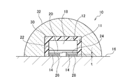
- the LED (Light Emitting Diode) package 10 shown in FIG. 1 includes a semiconductor light emitting device 11 as a bonded structure.
- the semiconductor light emitting device 11 has an LED chip 12 as a first structure and a ceramic substrate 16 as a second structure bonded to the LED chip 12 via a bonding portion 14 formed of a solder alloy.
- the joint portion 14 is formed by using a solder ball described later.
- the joint portion 14 has a thickness t of 3 ⁇ m or more and 50 ⁇ m or less.
- the thickness t of the joint portion 14 is the distance between the surfaces of the electrodes 22 and 24 which are the first joint surfaces and the surfaces of the electrodes 26 and 28 which are the second joint surfaces.
- the thickness t of the joint portion 14 is preferably 3 ⁇ m or more and less than 35 ⁇ m, and more preferably 3 ⁇ m or more and less than 20 ⁇ m. The thinner the thickness t of the joint portion 14, the better the thermal conductivity.
- the joint portion 14 is an Au—Sn-based alloy. Since the joint portion 14 is an Au—Sn-based alloy, the joint strength is higher than that of the Sn—Ag—Cu based alloy.
- the joint portion 14 is formed of a solder ball containing Sn in an amount of 19% by mass or more and 25% by mass or less and containing Au as a main component.
- the joint portion 14 may contain elements derived from the electrodes 22, 24, 26, 28 in addition to the elements derived from the solder balls.
- the joint portion 14 contains Sn in an amount of 19% by mass or more and 25% by mass or less, contains one or more of Fe, Cr, Ni, Cu, Co, and Ti, and the balance contains Au as a main component. Good.
- the balance may consist of Au and unavoidable impurities.
- the joint portion 14 includes a case where Sn is contained in an amount of 19% by mass or more and 25% by mass or less, an element of any one of Fe, Cr and Ni is contained, and the balance is mainly Au.
- the balance may consist of Au and unavoidable impurities.
- the concentration of Fe when Fe is contained is 0.1 mass ppm or more and 10 mass ppm or less
- the concentration of Cr when Cr is contained is 0.1 mass ppm or more and 100 mass by mass with respect to the entire joint portion 14. It is ppm or less
- the concentration of Ni when Ni is contained is 1 mass ppm or more and 5000 mass ppm or less.
- the LED chip 12 is covered with a covering portion 30, and the covering portion 30 is further covered with a lens portion 32.
- the covering portion 30 is formed of a transparent resin such as a silicone resin or an epoxy resin.
- the covering portion 30 may further contain a particulate phosphor.
- the lens portion 32 is formed by forming a silicone resin into a lens shape.
- the LED package 10 can select the color of the emitted light by the combination of the emission color of the LED chip 12 and the fluorescence color of the phosphor. For example, by setting the emission color of the LED chip 12 to blue and the fluorescence color of the phosphor to be yellow, white light can be emitted from the LED package 10.
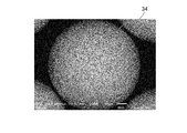
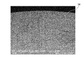
- the solder ball 34 according to the present embodiment shown in FIG. 3A is an Au—Sn-based alloy containing Sn in an amount of 19% by mass or more and 25% by mass or less and containing Au as a main component, among Fe, Cr, and Ni. It is a uniform eutectic alloy of Au 5 Sn 1 and Au Sn formed by containing at least one element. Therefore, the solder ball 34 has a good appearance because it can prevent the occurrence of shrinkage cavities on the surface (FIG. 3A).
- solder ball 34 Fe, Cr, and Ni are dispersed in a small amount in AuSn, so that there are many nucleation sites during solidification, and mainly without forming a non-uniform Au-rich phase during cooling.
- a uniform lamellar structure is formed by the first phase (also referred to as Au-rich phase) composed of Au 5 Sn and the second phase mainly composed of Au Sn (FIG. 3B). Therefore, the solder ball 34 according to the present embodiment can have a good appearance without shrinkage cavities due to the formation of a lamellar structure without a non-uniform Au-rich phase.
- the method for evaluating the uniformity of the lamellar structure of the solder ball 34 will be described below.
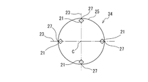
- the central cross section is a cross section including the center C of the solder ball 34.
- the frame 21 is a line segment having a length of 5 ⁇ m toward the center C from a position 27 where a line 23 passing through the center C of the solder ball 34 and parallel to the central cross section and an outer edge 25 of the solder ball 34 intersect.
- center and “center” are not limited to the case of perfect “center” and “center”, but include the case of being slightly deviated from the perfect "center” and "center”.
- the number of massive first phase (non-uniform Au-rich phase) 104 having a length and width of at least twice the distance between the first phase and the second phase in the lamellar structure is counted.
- the distance between the first phase and the second phase is the distance from the center of the first phase to the center of the second phase, and is, for example, a value measured by the rameller structure at the center of the solder ball 34.
- the center of the solder ball 34 may be, for example, a distance from the center of the solder ball 34 within a range of 10% of the diameter of the solder ball 34.
- the distance between the first phase and the second phase is, for example, about 0.1 ⁇ m to 0.5 ⁇ m.
- the vertical and horizontal lengths are lengths in any two orthogonal directions in the central cross section, and the vertical and horizontal lengths may be at least twice the distance between the first phase and the second phase, respectively, and have the same length. Not limited to being.
- the lumpy first phase 104 is formed continuously with the uniform first phase in the lamellar structure.
- the average number of the massive first phase 104 in each frame 21 is 3 or less. If the average number of the massive first phase 104 is 3 or less, it can be said that a uniform lamellar structure is formed in the vicinity of the surface of the solder balls 34. As shown in FIG. 3B, the solder ball 34 does not have a lumpy first phase.
- the solder ball 34 contains Sn in an amount of 19% by mass or more and 25% by mass or less, contains any one or more elements of Fe, Cr, Ni, Cu, Co, and Ti, and the balance contains Au as a main component. Including the case.
- the balance may consist of Au and unavoidable impurities.
- the solder ball 34 includes a case where Sn is contained in an amount of 19% by mass or more and 25% by mass or less, an element of any one of Fe, Cr, and Ni is contained, and the balance is mainly Au.
- the balance may consist of Au and unavoidable impurities.
- the concentration of Fe when Fe is contained is 0.1 mass ppm or more and 10 mass ppm or less
- the concentration of Cr when Cr is contained is 0.1 mass ppm or more and 100 mass by mass with respect to the entire solder ball 34. It is ppm or less
- the concentration of Ni when Ni is contained is 1 mass ppm or more and 5000 mass ppm or less.
- the solder ball 34 prevents the occurrence of shrinkage cavities and provides good wettability. That is, the solder ball 34 has a lamellar structure without a non-uniform Au-rich phase, so that a good appearance without shrinkage cavities can be obtained. Further, when the concentration of the element is within the above range, the solder ball 34 can obtain good wettability by surely dissolving the oxide film on the surface at the time of melting. It is considered that the reason why the required concentration range differs depending on each element of Fe, Cr, and Ni is that the affinity between Au and Sn when they become solidified nuclei and Fe, Cr, and Ni has an influence.
- the concentration of Ni is 1000 mass ppm or more and 5000 mass ppm or less, a solder ball having no unevenness and shrinkage can be obtained, which is more preferable, and when it is 3800 mass ppm or less, higher productivity can be obtained.
- the concentration of Ni is 1300 mass ppm or more and 2500 mass ppm or less, further excellent wettability can be obtained.
- the solder ball 34 contains 19% by mass or more and 25% by mass or less of Sn, contains an element combination of any two or more of Fe, Cr, and Ni, and includes a case where the balance contains Au as a main component.
- the balance may consist of Au and unavoidable impurities.
- the concentration of Ni may be in the range of 0 mass ppm or more and 4890 mass ppm or less.
- the total concentration of the element combinations may be more than 0.1 mass ppm and 500 mass ppm or less, and the concentration of Ni in this case can be in the range of 0 mass ppm or more and 450 mass ppm or less.
- Concentration analysis method An element concentration analysis method will be described. The element concentration is analyzed separately for ICP-MS and ICP-OES according to the concentration range. If the concentration range is less than 100 mass ppm, it can be analyzed by inductively coupled plasma mass spectrometry (ICP-MS). When the concentration range is 100 mass ppm or more, it can be analyzed by inductively coupled plasma optical emission spectrometer (ICP-OES).
- ICP-MS inductively coupled plasma mass spectrometry
- ICP-OES inductively coupled plasma optical emission spectrometer
- Example pretreatment method As the analyzer, Agilent Technologies Co., Ltd. (device model number: Agilent8800 type) is used. The procedure of pretreatment is as follows. Weigh 0.1 g of solder balls, add 20 ml of aqua regia (composition: hydrochloric acid and nitric acid mixed at a ratio of 3: 1), and heat to about 200 ° C. to dissolve. After allowing to cool, transfer to a polypropylene (hereinafter referred to as “PP”) volumetric flask (capacity: 100 mL) and incubate with ultrapure water. A quartz glass beaker is used for the decomposition container in order to avoid contamination with impurities.
- PP polypropylene
- ⁇ Analysis method> The standard addition method is adopted as the analysis method. Specifically, 10 mL each of the solution is placed in a plurality of PP volumetric flasks (volume: 100 mL), and 100 ⁇ g of a single element standard solution of the target element to be analyzed (Fe, Cr, Ni) is placed in the PP volumetric flask. After 2 mL of the solution diluted to / L is added stepwise, the extrapolated value when the addition amount is assumed to be zero is used as the analytical value of the target element based on the analytical values of the defined solutions. Reagents manufactured by Kanto Chemical Co., Inc. (Fe: 20247-2B, Cr: 08037-3B, Ni: 28577-2B) are used as the single element standard solution.
- ⁇ Analysis method> The standard addition method is adopted as the analysis method. Specifically, 10 mL each of the solution is placed in a plurality of glass volumetric flasks (volume: 100 mL), and in particular, a single element standard solution (1000 ⁇ g) of the target element to be analyzed (Fe, Cr, Ni) is placed in the PP volumetric flask. After adding 0.1 mL each of / L) stepwise, the extrapolated value when the addition amount is assumed to be zero is used as the analytical value of the target element based on each analytical value of the constant volume solution. Reagents manufactured by Kanto Chemical Co., Inc. (Fe: 20247-2B, Cr: 08037-3B, Ni: 28577-2B) are used as the single element standard solution.
- the nozzle 35 has a cylindrical shape, and the outlet 47 opens at the lower end of the cylinder.
- the nozzle pedestal 39 can hold the nozzle 35 slidably in the vertical direction by arranging the nozzle 35 in a cylindrical vertical opening having the same diameter as the cylindrical portion of the nozzle 35.
- the vibrating device 37, the connecting rod 49, and the nozzle 35 are arranged in the vertical direction, and the nozzle 35 vibrates in the vertical direction by the vibrating device 37.
- the frequency is set to 10 to 50 kHz.
- the molten solder 33 is held at a temperature higher than the melting point by a predetermined temperature.
- a heating device in which a band heater is wound around a solder storage tank 41 is provided, and the temperature of the molten solder 33 can be maintained at a temperature 100 ° C. or higher higher than its melting point.
- the size of the solder ball 34 to be manufactured is determined by the diameter of the outlet 47, the outflow speed of the molten solder 33 from the outlet 47, and the frequency of the applied vibration. Further, the outflow rate of the molten solder 33 from the outflow port 47 can be adjusted by the head difference between the liquid level in the solder storage tank 41 and the outflow port 47.
- the diameter of the outlet 47 is about 53 to 57 ⁇ m
- the head difference between the liquid level in the solder storage tank 41 and the outlet 47 is about 0.3 to 0.4 MPa.
- the frequency of nozzle vibration may be selected in the range of 3.0 to 4.0 kHz.
- the manufacturing apparatus 31 can generate a solder ball 34 having a uniform droplet size and a highly accurate ball diameter.
- solder balls 34 are arranged on the electrodes 22 and 24 of the LED chip 12 and temporarily fixed. As shown in FIG. 6A, the solder balls 34 may be arranged so as to be close-packed. When placing the solder balls 34 so as to be close-packed, the distance between the solder balls 34 is a spherical diameter R 1 of the solder balls 34. The region on the electrodes 22 and 24 on which the solder balls 34 are arranged is appropriately selected so that the thickness of the joint portion 14 after joining is within a desired range.
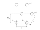
- solder balls 34 may be arranged on the electrodes 22 and 24 at intervals L represented by the following formula (1).
- L ⁇ (2R 1 3 / 3t) (1)
- FIG. 6B shows an example in which the solder balls 34 are arranged in a zigzag shape
- the solder balls 34 may be arranged in a grid pattern or a straight line.
- the bump forming method can also be used when the solder balls 34 are arranged in a zigzag shape or a grid pattern at predetermined intervals.
- the LED chip 12 is directed toward the second bonding surface which is the surface of the electrodes 26 and 28 with the first bonding surface which is the surface of the electrodes 22 and 24 facing. Is installed upside down on the ceramic substrate 16, and the LED chip 12 and the ceramic substrate 16 are aligned so that the electrodes 22 and 24 and the electrodes 26 and 28 correspond to each other. By heating in this state, the solder balls 34 are melted, cooled and solidified to form a joint portion 14, and the electrodes 22 and 24 and the electrodes 26 and 28 are electrically connected.
- the LED chip 12 may be heated to reflow the solder balls 34.
- the solder balls 34 are wetted and spread on the electrodes 22 and 24 by the reflow, and become a solidified joint 14 by cooling.
- the LED chip 12 is installed upside down on the ceramic substrate 16, and the LED chip 12 and the ceramic substrate 16 are aligned and heated so that the electrodes 22 and 24 and the electrodes 26 and 28 correspond to each other.
- the electrodes 22 and 24 and the electrodes 26 and 28 are electrically connected by melting, cooling and solidifying the joint portion 14 again. In this case, since the joint portion 14 is wet and spread in advance, the electrodes 22 and 24 and the electrodes 26 and 28 can be more reliably connected, and the occurrence of voids and the like can be more reliably reduced.
- the LED package 10 formed as described above is generated by the LED chip 12 because the thickness t of the joint portion 14 is 50 ⁇ m or less and the LED chip 12 and the ceramic substrate 16 are in close proximity to each other.
- the heat can be efficiently transferred to the ceramic substrate 16. Therefore, since the LED package 10 can improve the heat dissipation property, the quality of the semiconductor light emitting device 11 can be improved.
- the thickness t of the joint portion 14 is preferably less than 35 ⁇ m, more preferably 20 ⁇ m or less.
- the solder ball 34 has a uniform lamellar structure formed by containing the above elements in a predetermined concentration range, and the appearance is in a good state without shrinkage cavities, so that the reliability can be improved.
- a solder ball 34 having uniform ball diameter accuracy can be obtained.
- the reliability of the LED package 10 can be further improved by joining using the solder balls 34 having uniform ball diameter accuracy.
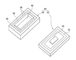
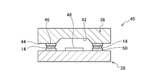
- the sealing package 40 as the bonded structure shown in FIG. 8 includes a lid (lid) 36 as the first structure and a base 38 as the second structure.
- the lid 36 is a flat plate-shaped member, and has a container portion 42 in the center and a flange portion 44 formed so as to surround the container portion 42.
- the surface of the container portion 42 is formed into a concave shape in the thickness direction.
- a conductive layer 46 made of a conductive material and a solder ball 34 are arranged on the conductive layer 46.
- the base 38 is a flat plate-shaped member, the electronic device 48 is fixed in the center, and a conductive layer 50 formed of a conductive material is formed so as to surround the electronic device 48.
- the electronic device 48 is, for example, a SAW filter, an FBAR filter, and a crystal oscillator.
- the lid 36 may be a flat member on which the container portion is not formed and the conductive layer is formed at a position corresponding to the conductive layer formed on the flange portion of the base.
- the joint portion 14 shown in FIG. 10B has a basic joint portion 59 and an expansion portion 60.
- the basic joint portion 59 and the extension portion 60 are integrally formed.
- the basic joint portion 59 is formed by arranging solder balls 34 one by one in the height direction at predetermined intervals, and joins the joint portions 14 per unit length in the longitudinal direction (arrows A1 and A2 in FIG. 10B).
- the area is constant.
- the width and length of the basic joint portion 59 are constant.
- the expansion portion 60 has a larger joint area than the basic joint portion 59.
- the expansion portion 60 is provided at a corner portion where the basic joint portion 59 is bent.
- the broken line in FIG. 10B is a virtual line indicating the outer edge of the corner portion of the basic joint portion 59, assuming that the expansion portion 60 is not formed.
- Constant is not limited to the case where it is completely constant, but includes a certain range, for example, a range that can be said to be a manufacturing error.
- FIG. 10A shows a case where two solder balls 34 are stacked, but the present invention is not limited to this, and three or more solder balls may be stacked.
- FIG. 10B shows a corner portion where the basic joint portion 59 is bent at a right angle, but the present invention is not limited to this, and the angle at which the basic joint portion 59 is bent at the corner portion can be arbitrarily selected.
- the expansion portions may be formed at regular intervals in a region other than the corner portion, for example, in a straight portion as shown in FIG.
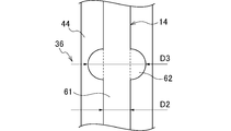
- the joint portion 14 shown in FIG. 11 has a linear basic joint portion 61 and an extension portion 62 at a predetermined position of the basic joint portion 61.
- the basic joint portion 61 and the extension portion 62 are integrally formed.
- the broken line in FIG. 11 is a virtual line indicating the outer edge of the basic joint portion 61, assuming that the extension portion 62 is not formed.
- the width and length of the basic joint portion 61 are constant, and the joint area per unit length in the longitudinal direction is constant.
- the extension portion 62 is continuously formed on the outer edge of the straight portion of the basic joint portion 61, and has a contour extending outward in the width direction.
- the contour shown in FIG. 11 is arcuate, but the present invention is not limited to this.
- the width D3 of the expansion portion 62 is longer than the width D2 of the basic joint portion 61.
- the joint area is increased by providing the expansion portions at regular intervals, the mechanical strength can be improved, and the electrical conductivity and the thermal conductivity can be further improved.
- the present invention is not limited to the above embodiment, and can be appropriately modified within the scope of the gist of the present invention.
- the present invention is not limited to this, and the present invention is also applicable to the laser diode.
- solder balls shown in Table 1 were produced by the procedure described in the above "(3) Manufacturing method (solder balls)", and their appearance and wettability were evaluated.
- solder balls In preparing the solder balls, first, Au and Sn and the added elements were weighed so as to have the composition shown in Table 1, and an ingot was prepared by high-frequency dissolution. The ingot was placed in a solder storage tank, the solder storage tank was heated to 300 to 400 ° C., and the frequency of the piezo element was adjusted to 10 to 50 kHz.
- the solder reservoir within, N 2 -5 vol% H 2 atmosphere and, by the positive pressure, the solder balls to prepare the 10,000 or more, any 50 were evaluated as follows.
- the concentration of each solder ball was analyzed by ICP-MS or ICP-OES.
- the concentration of Cr in the case where the joint contains any one of Fe, Cr, and Ni, and the concentration of Cr in the entire solder ball is 0.1. Since the mass is ppm or more and 100 mass ppm or less, a solder ball having no unevenness and shrinkage cavities and having good wettability was obtained.
- Example No. 16 to 29 when the joint portion contains any one element of Fe, Cr, and Ni, and Ni is contained in the entire solder ball, the concentration of Ni is 1 mass ppm. Since it was 5000 mass ppm or less, a solder ball having no shrinkage cavities and having better wettability was obtained.
- Example No. Nos. 17 to 21 have a Ni concentration of 20 mass ppm or more and 50 mass ppm or less. Since the concentration of Ni in Nos. 24 to 29 was 1000 mass ppm or more and 5000 mass ppm or less, solder balls having no appearance defects due to unevenness and shrinkage cavities were obtained. In Examples No. 25 to 27, since the Ni concentration was 1300 mass ppm or more and 2500 mass ppm or less, further excellent results were obtained in terms of wettability.
- the joint portion contains a combination of two or more elements of Fe, Cr, and Ni, and the concentrations of Fe and Cr among the elements are as described above. It is a concentration range, and the concentration of Ni is in the range of 0 mass ppm or more and 4990 mass ppm or less, and the total concentration of the element combination with respect to the entire solder ball is more than 0.1 mass ppm and 5000 mass ppm or less. A solder ball having no unevenness and shrinkage cavities and having good wettability was obtained.
- Comparative Examples Nos. 1, 3 and 5 did not contain any of Fe, Cr and Ni, so that shrinkage cavities occurred.
- Comparative Examples No. 2 and 4 since the concentrations of Fe and Cr each exceeded the upper limit values, the wettability was lowered. Comparative Example No. In No. 6, the concentration of Ni exceeded the upper limit value, and uniform ball granulation could not be performed.
Landscapes
- Engineering & Computer Science (AREA)
- Mechanical Engineering (AREA)
- Chemical & Material Sciences (AREA)
- Materials Engineering (AREA)
- Metallurgy (AREA)
- Organic Chemistry (AREA)
- Electric Connection Of Electric Components To Printed Circuits (AREA)
Abstract
品質を向上することができる接合構造体、接合構造体の製造方法及びハンダボールを提供する。第1構造体12と、Au-Sn系合金で形成された接合部14を介して前記第1構造体12に接合された第2構造体16と、を備えた接合構造体11であって、前記接合部14の厚さtが3μm以上50μm以下である。
Description
本発明は、接合構造体、接合構造体の製造方法及びハンダボールに関するものである。
接合構造体として、半導体発光装置や、デバイスを気密封止する封止パッケージが知られている。半導体発光装置は、半導体発光素子と、半導体発光素子を実装する回路基板とを有する。封止パッケージは、電子デバイスとして、例えばSAW(Surface Acoustic Wave)フィルタ、FBAR(Film Bulk Acoustic Resonator)フィルタ、水晶振動子を気密封止している。これらの接合構造体の接合材として、高強度性、高電気伝導性などの観点から、Au-Sn系合金で形成された、ハンダペーストや、シート状のろう材が用いられる(例えば、特許文献1、2)。
特許文献1に、AuSn粉末とフラックスを含むハンダペーストが開示されている。特許文献1のハンダペーストは、粉末を構成する粒子を、酸化されやすい粒子の外側の層へ向かうにしたがって、Auの割合が多くなる構造とすることによって、酸化を抑制している。
特許文献2に、AuSnのろう材のテープを備えたキャップが開示されている。特許文献2のキャップは、AuSnのろう材のテープと、FeNi系材料にNi又はAuめっきを施した基材のテープとを重ねてろう材と基材とを加熱融着したクラッド材を、プレス抜きすることによって得られる。
上記特許文献1のようなハンダペーストを用いた接合では、AuSn合金粒子をフラックス中に分散させて使用するため、リフロー時に、一部分においてAuSn合金粒子同士が合体しない孤立した状態となる、部分未融合接合が生じる可能性がある。加えて、AuSn合金粒子同士が合体する際に、フラックス等を内部に内包した異物内包接合が生じる可能性がある。また、印刷や吐出などによって接合箇所に所定量のハンダペーストを供給する必要があるため、リフロー後の接合部の厚さを薄くすることが難しい。上述したように、AuSn合金粒子を溶融合体させるペースト接合では、部分未融合接合や異物内包接合を形成する可能性が高く、接合部の厚さを薄くすることが難しいため、電気伝導性、熱伝導性、又は気密性が損なわれ、品質を向上することが困難である、という問題があった。
また上記特許文献2のようなシート状のろう材は、材料が硬く脆いため、厚さを薄くすることが難しく、シート状のろう材を溶融して形成された接合部も厚さが厚くなるため、熱伝導性などの品質を向上することが困難であるという問題があった。
上記特許文献1のようなハンダペーストを用いた接合では、印刷や吐出などによって接合箇所に所定量のハンダペーストを供給する必要があるため、Auの使用量を削減するには限界があった。また上記特許文献2のようなシート状のろう材は、クラッド材からプレス抜きすることによって所定の大きさ及び形状とするため、プレス抜きされた残りのクラッド材が無駄となり、歩留りが低く、結果としてAuの使用量を削減することが困難であるという問題があった。
ハンダペーストやろう材のテープに替えてAu-Sn系合金のハンダボールを使用することによって、Auの使用量を削減することが期待できる。一方、Au-Sn系合金のハンダボールは、引け巣による外観不良が生じる、という問題があった。
本発明は、品質を向上することができる接合構造体及び接合構造体の製造方法を提供することを第1の目的とする。
本発明は、引け巣による外観不良の発生を防止することができるハンダボールを提供することを第2の目的とする。
本発明に係る接合構造体は、第1構造体と、Au-Sn系合金で形成された接合部を介して前記第1構造体に接合された第2構造体と、を備えた接合構造体であって、前記接合部の厚さが3μm以上50μm以下である。
本発明に係る接合構造体の製造方法は、第1構造体と、Au-Sn系合金で形成された接合部を介して前記第1構造体に接合された第2構造体と、を備えた接合構造体の製造方法であって、前記第1構造体の第1接合面に前記Au-Sn系合金で形成されたハンダボールを固定するボール固定工程と、前記第1接合面を前記第2構造体の第2接合面に向けて、前記第2構造体に対して前記第1構造体を裏返して、前記第1接合面と前記第2接合面を電気的に接続する工程と、を備え、前記接合部の厚さが3μm以上50μm以下である。
本発明に係るハンダボールは、Snを19質量%以上25質量%以下含有し、残部がAuを主成分とするハンダボールであって、Fe、Cr、Niのいずれか1種の元素を含有し、前記ハンダボール全体に対する、Feを含む場合のFeの濃度が0.1質量ppm以上10質量ppm以下であり、Crを含む場合のCrの濃度が0.1質量ppm以上100質量ppm以下であり、Niを含む場合のNiの濃度が1質量ppm以上5000質量ppm以下である。
本発明に係るハンダボールは、Snを19質量%以上25質量%以下含有し、残部がAuを主成分とするハンダボールであって、Fe、Cr、Niから選ばれる少なくとも2種以上の元素組合せを含有し、前記ハンダボール全体に対する前記元素組合せの濃度の合計が0.1質量ppm超5000質量ppm以下であり、Feを含む場合のFeの濃度が0.1質量ppm以上10質量ppm以下であり、Crを含む場合のCrの濃度が0.1質量ppm以上100質量ppm以下であり、Niの濃度が0質量ppm以上4990質量ppm以下の範囲である。
本発明に係るハンダボールは、Snを19質量%以上25質量%以下含有し、残部がAuを主成分とするハンダボールであって、前記ハンダボールの中央断面は、主にAu5Snからなる第1相と主にAuSnからなる第2相とで構成されたラメラー組織を含み、前記ハンダボールの中心を通り前記中央断面に平行な線と前記ハンダボールの外縁が交差する位置から、前記中心に向かって5μmの長さの線分を対角線として有する、前記ハンダボールの周方向に均等に4個配置された、正方形の枠内において、前記第1相と前記第2相の間隔の2倍以上の縦横長さを有する塊状の前記第1相が、平均で3個以下である。
本発明によれば、接合部の厚さが3μm以上50μm以下であることによって、熱伝導性が高く、接合構造体としての品質を向上することができる。
本発明によれば、AuとSnによる均一な共晶合金が得られ、ハンダボール表面の引け巣による外観不良の発生を防止することができる。
以下、図面を参照して本発明の実施形態について詳細に説明する。同様の構成には同様の符号を付し、説明を適宜省略する。
1.第1実施形態
(1)接合構造体
図1に示すLED(Light Emitting Diode)パッケージ10は、接合構造体としての半導体発光装置11を備える。半導体発光装置11は、第1構造体としてのLEDチップ12と、ハンダ合金で形成された接合部14を介してLEDチップ12に接合された第2構造体としてのセラミック基板16とを有する。
(1)接合構造体
図1に示すLED(Light Emitting Diode)パッケージ10は、接合構造体としての半導体発光装置11を備える。半導体発光装置11は、第1構造体としてのLEDチップ12と、ハンダ合金で形成された接合部14を介してLEDチップ12に接合された第2構造体としてのセラミック基板16とを有する。
LEDチップ12は、基板20と、基板20上に形成され発光層を含む結晶層18とを有する発光素子である。基板20の結晶層18が形成された側と反対側の表面に、電極22と電極24が形成されている。電極22と電極24は、Au、Ag、Cu、Al等の導電材料からなる。LEDチップ12は、電極22,24が下側を向いたフリップチップ型の発光素子である。電極22,24は、一方がn側電極で、他方がp側電極である。
セラミック基板16は、放熱性に優れた基板を用いるのが好ましく、例えば窒化アルミニウム基板(AIN)、熱伝導性の高い窒化珪素基板(Si3N4)、DCB基板(アルミナ系酸化物セラミック基板に銅回路板を、直接接合したもの)を用いることができる。セラミック基板16上には、電極26と電極28が形成されている。電極26と電極28は、電極22,24と同様の材料で形成されており、電極22,24の材料と同種であってもよいし、異なっていてもよい。
接合部14は、後述するハンダボールを用いて形成されている。接合部14は、厚さtが3μm以上50μm以下である。接合部14の厚さtは、第1接合面である電極22,24の表面と、第2接合面である電極26,28の表面の間の距離である。接合部14の厚さtが上記範囲内であることによって、LEDチップ12とセラミック基板16が近接することになり、LEDチップ12で生じた熱をセラミック基板16へ効率的に伝達することができる。接合部14の厚さtは、好ましくは3μm以上35μm未満、より好ましくは3μm以上20μm未満である。接合部14の厚さtは薄いほど、熱伝導性を向上することができる。
接合部14は、Au-Sn系合金である。接合部14は、Au-Sn系合金であることによって、Sn-Ag-Cu系合金に比べ、接合強度が高い。接合部14は、Snを19質量%以上25質量%以下含有し、Auを主成分とするハンダボールで形成される。接合部14は、ハンダボールに由来する元素に加え、電極22,24,26,28に由来する元素を含む場合がある。
接合部14は、Snを19質量%以上25質量%以下含有し、Fe、Cr、Ni、Cu、Co、Tiのうちいずれか1種以上の元素を含有し、残部がAuを主成分としてもよい。前記残部は、Auと不可避不純物からなるとしてもよい。
接合部14は、Snを19質量%以上25質量%以下含有し、Fe、Cr、Niのうちいずれか1種の元素を含有し、残部がAuを主成分とする場合を含む。前記残部は、Auと不可避不純物からなるとしてもよい。接合部14は、接合部14全体に対する、Feを含む場合のFeの濃度が0.1質量ppm以上10質量ppm以下であり、Crを含む場合のCrの濃度が0.1質量ppm以上100質量ppm以下であり、Niを含む場合のNiの濃度が1質量ppm以上5000質量ppm以下である。
また接合部14は、Snを19質量%以上25質量%以下含有し、Fe、Cr、Niのうちいずれか2種以上の元素組合せを含有し、残部がAuを主成分とする場合を含む。前記残部は、Auと不可避不純物からなるとしてもよい。上記元素のうちFe、Crのそれぞれの濃度は、上記濃度範囲であって、Niの濃度が0質量ppm以上4990質量ppm以下の範囲であり、かつ、接合部14全体に対する上記元素組合せの濃度の合計が0.1質量ppm超5000質量ppm以下である。各濃度範囲については、後に詳述する。
LEDチップ12は、被覆部30で覆われており、さらに被覆部30がレンズ部32で覆われている。被覆部30は、シリコーン樹脂やエポキシ樹脂などの透明樹脂で形成されている。被覆部30は、さらに粒子状の蛍光体を含有してもよい。レンズ部32は、シリコーン樹脂をレンズ状に形成してなる。LEDパッケージ10は、LEDチップ12の発光色と前記蛍光体の蛍光色の組み合わせによって、発光する光の色を選択することができる。例えば、LEDチップ12の発光色を青色とし、前記蛍光体の蛍光色を黄色とすることによって、LEDパッケージ10から白色の光を発光させることができる。
(2)ハンダボール
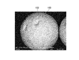
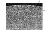
図2Aに示すように、従来のAu-Sn系合金のハンダボール100は、表面に凹凸102が生じ、場合によっては引け巣による外観不良が生じる、という問題があった。ハンダボール100は、断面において表面近傍に不均一なAuリッチ相104が生成されていることが確認された(図2B)。このことから引け巣は、不均一なAuリッチ相104の発生に大きく影響されると考えられる。
図2Aに示すように、従来のAu-Sn系合金のハンダボール100は、表面に凹凸102が生じ、場合によっては引け巣による外観不良が生じる、という問題があった。ハンダボール100は、断面において表面近傍に不均一なAuリッチ相104が生成されていることが確認された(図2B)。このことから引け巣は、不均一なAuリッチ相104の発生に大きく影響されると考えられる。
図3Aに示す本実施形態に係るハンダボール34は、Snを19質量%以上25質量%以下含有し、Auを主成分とする、Au-Sn系合金であって、Fe、Cr、Niのうち少なくとも1種以上の元素を含有することによって形成された、Au5Sn1とAuSnによる均一な共晶合金である。したがってハンダボール34は、表面の引け巣の発生を防止することができるので、外観が良好である(図3A)。
ハンダボール34は、Fe、Cr、Niが微量にAuSn内に分散していることで、凝固時の核生成サイトが多数存在し、冷却時に不均一なAuリッチ相を生成することなく、主にAu5Snからなる第1相(Auリッチ相ともいう)と、主にAuSnからなる第2相とによる均一なラメラー組織が形成される(図3B)。したがって本実施形態に係るハンダボール34は、不均一なAuリッチ相がない、ラメラー組織が形成されていることによって、外観を引け巣のない良好な状態にすることができる。
以下にハンダボール34のラメラー組織の均一性を評価する方法を説明する。まず、図4Aに示すように、ハンダボール34の中央断面において、周方向に均等に正方形の枠21を4個配置する。中央断面は、ハンダボール34の中心Cを含む断面である。前記枠21は、前記ハンダボール34の中心Cを通り前記中央断面に平行な線23と前記ハンダボール34の外縁25が交差する位置27から、前記中心Cに向かって5μmの長さの線分を対角線として有する。なお、本明細書において「中央」及び「中心」は、完全な「中央」及び「中心」である場合に限定されず、完全な「中央」及び「中心」から多少ずれている場合を含む。
次に、各枠21について、ラメラー組織における第1相と第2相の間隔の2倍以上の縦横長さを有する塊状の第1相(不均一なAuリッチ相)104の個数をカウントする。第1相と第2相の間隔は、第1相の中心から第2相の中心までの距離であり、例えば、ハンダボール34中央におけるラメラー組織で測定した値とする。ハンダボール34中央とは、例えば、ハンダボール34の中心からの距離がハンダボール34の直径の10%の範囲内としてもよい。第1相と第2相の間隔は、例えば、0.1μm~0.5μm程度である。縦横長さは、中央断面における任意の直交する2方向の長さであり、縦長さ及び横長さが、それぞれ第1相と第2相の間隔の2倍以上であればよく、同じ長さであることに限定されない。塊状の前記第1相104は、ラメラー組織における均一な第1相と連続して形成されている。
ハンダボール34は、各枠21における塊状の前記第1相104の個数の平均が3個以下であるのが好ましい。上記塊状の前記第1相104の個数の平均が3個以下であれば、ハンダボール34の表面近傍において、均一なラメラー組織が形成されているといえる。図3Bに示したように、ハンダボール34は、塊状の第1相が認められない。
一方、図4Bに示した従来のAu-Sn系合金のハンダボール100は、枠21に少なくとも30個の塊状の前記第1相104が認められ、4個の枠21の平均が約15個であり、ゆうに3個を超えていた。
ハンダボール34は、Snを19質量%以上25質量%以下含有し、Fe、Cr、Ni、Cu、Co、Tiのうちいずれか1種以上の元素を含有し、残部がAuを主成分とする場合を含む。前記残部は、Auと不可避不純物からなるとしてもよい。ハンダボール34は、上記元素を含有することによって、不均一なAuリッチ相がない、ラメラー組織が形成され、外観を引け巣のない良好な状態にすることができる。
ハンダボール34の球径は40μm~250μmが好ましく、50μm~250μmであるのがより好ましい。40μm~250μmの球径であれば、均一な球径精度のハンダボール34を製造することができる。
ハンダボール34は、Au-19質量%SnよりもAuの濃度が高い組成の場合、Auリッチ相が容易に析出し、凹凸や引け巣が発生しやすくなる。Snの濃度が19質量%未満及び25質量%超の組成の場合、液相線温度が高くなり、固液共存領域が広く存在するため、均一な凝固組織を得ることが難しい。
ハンダボール34は、Snを19質量%以上25質量%以下含有し、Fe、Cr、Niのうちいずれか1種の元素を含有し、残部がAuを主成分とする場合を含む。前記残部は、Auと不可避不純物からなるとしてもよい。ハンダボール34は、ハンダボール34全体に対する、Feを含む場合のFeの濃度が0.1質量ppm以上10質量ppm以下であり、Crを含む場合のCrの濃度が0.1質量ppm以上100質量ppm以下であり、Niを含む場合のNiの濃度が1質量ppm以上5000質量ppm以下である。
ハンダボール34は、上記元素の濃度が上記範囲内である場合、引け巣の発生を防止すると共に、良好な濡れ性が得られる。すなわちハンダボール34は、不均一なAuリッチ相がない、ラメラー組織が形成されるので、引け巣のない良好な外観が得られる。またハンダボール34は、上記元素の濃度が上記範囲内である場合、溶融時に表面の酸化膜が確実に溶解することによって、良好な濡れ性が得られる。Fe、Cr、Niの各元素によって必要な濃度範囲が異なる理由は、凝固核となる際のAuやSnとFe、Cr、Niとの親和性が影響しているものと考えられる。
一方、上記元素の濃度が上記下限値未満の場合、上記Auリッチ相の析出を防止する効果が得られない。また、上記元素の濃度が上記上限値超の場合、ハンダボールの濡れ性が低下する。濡れ性は、ハンダボール表面の酸化膜による影響を受けていると考えられる。すなわち、上記濃度範囲が上限値以下の場合に比べ、上限値超の場合に形成される酸化膜は、厚みが厚かったり、厚みは同等でも構造が異なる場合がある。上限値超の場合、ハンダボールの溶融時に、上記酸化膜が溶解しにくいことによって、濡れ性が低下すると考えられる。
上記Feの濃度は、0.1質量ppm以上5質量ppm以下であるのが好ましい。Feの濃度が0.1質量ppm以上5質量ppm以下であると、より優れた濡れ性が得られる。上記Niの濃度は、1質量ppm以上5000質量ppm以下であることによって、引け巣の発生が防止できると共に、より優れた濡れ性が得られる。Niの濃度が20質量ppm以上50質量ppm以下であると、凹凸及び引け巣がないハンダボールが得られるので、より好ましい。また、Niの濃度が1000質量ppm以上5000質量ppm以下であると、凹凸及び引け巣がないハンダボールが得られるのでより好ましく、3800質量ppm以下であると、より高い生産性が得られる。Niの濃度が1300質量ppm以上2500質量ppm以下であると、さらに優れた濡れ性が得られる。
ハンダボール34は、Snを19質量%以上25質量%以下含有し、Fe、Cr、Niのうちいずれか2種以上の元素組合せを含有し、残部がAuを主成分とする場合を含む。前記残部は、Auと不可避不純物からなるとしてもよい。ハンダボール34は、Feを含む場合のFeの濃度が0.1質量ppm以上10質量ppm以下であり、Crを含む場合のCrの濃度が0.1質量ppm以上100質量ppm以下であり、Niの濃度が0質量ppm以上4990質量ppm以下の範囲であり、かつ、ハンダボール34全体に対する前記元素組合せの濃度の合計が0.1質量ppm超5000質量ppm以下である。前記元素組合せの濃度の合計が上記下限値未満の場合、上記Auリッチ相の析出を防止する効果が得られない。一方、前記元素組合せの濃度の合計が5000質量ppmを超える場合、ハンダボールの濡れ性が低下するもしくは、造粒性が悪くなる。Niの濃度は、0質量ppm以上4890質量ppm以下の範囲としてもよい。前記元素組合せの濃度の合計は0.1質量ppm超500質量ppm以下としてもよく、この場合のNiの濃度は0質量ppm以上450質量ppm以下の範囲とすることができる。元素組合せの濃度の合計が0.1質量ppm超500質量ppm以下の場合、より確実に、凹凸及び引け巣がないハンダボールが得られると共に、より優れた濡れ性が得られる。
(3)濃度の分析方法
元素濃度の分析方法について説明する。元素濃度は、濃度範囲により、ICP-MSとICP-OESとで分けて分析する。濃度範囲が100質量ppm未満の場合、誘導結合プラズマ質量分析法(ICP-MS; Inductively coupled plasma mass spectrometry)によって分析することができる。濃度範囲が100質量ppm以上の場合、誘導結合プラズマ発光分光分析法(ICP-OES; Inductively coupled plasma optical emission spectrometer)によって分析することができる。
元素濃度の分析方法について説明する。元素濃度は、濃度範囲により、ICP-MSとICP-OESとで分けて分析する。濃度範囲が100質量ppm未満の場合、誘導結合プラズマ質量分析法(ICP-MS; Inductively coupled plasma mass spectrometry)によって分析することができる。濃度範囲が100質量ppm以上の場合、誘導結合プラズマ発光分光分析法(ICP-OES; Inductively coupled plasma optical emission spectrometer)によって分析することができる。
(ICP-MSについて)
〈試料前処理法〉
分析装置には、アジレント・テクノロジー(株)製(装置型番:Agilent8800型)を用いる。前処理の要領は以下のとおりである。はんだボールを0.1gはかりとり、20mlの王水(組成:塩酸と硝酸を3:1の割合で混合)を加え、約200℃に加熱し、溶解する。放冷後、ポリプロピレン製(以下「PP製」)メスフラスコ(容量:100mL)に移し入れ、超純水で定容する。分解容器には、不純物の混入を回避するために石英ガラス製ビーカーを用いる。
〈試料前処理法〉
分析装置には、アジレント・テクノロジー(株)製(装置型番:Agilent8800型)を用いる。前処理の要領は以下のとおりである。はんだボールを0.1gはかりとり、20mlの王水(組成:塩酸と硝酸を3:1の割合で混合)を加え、約200℃に加熱し、溶解する。放冷後、ポリプロピレン製(以下「PP製」)メスフラスコ(容量:100mL)に移し入れ、超純水で定容する。分解容器には、不純物の混入を回避するために石英ガラス製ビーカーを用いる。
〈分析方法〉
分析方法には、標準添加法を採用する。具体的には、溶液を複数のPP製メスフラスコ(容量:100mL)にそれぞれ10mLずつをとりわけ、当該PP製メスフラスコに目的の分析対象元素(Fe、Cr、Ni)の単元素標準液を100μg/Lに希釈した溶液を2mLずつ段階的に添加後、定容した溶液のそれぞれの分析値をもとに、添加量がゼロと仮定したときの外挿値を目的元素の分析値とする。単元素標準液には関東化学製の試薬(Fe:20247-2B、Cr:08037-3B、Ni:28577-2B)を用いる。
分析方法には、標準添加法を採用する。具体的には、溶液を複数のPP製メスフラスコ(容量:100mL)にそれぞれ10mLずつをとりわけ、当該PP製メスフラスコに目的の分析対象元素(Fe、Cr、Ni)の単元素標準液を100μg/Lに希釈した溶液を2mLずつ段階的に添加後、定容した溶液のそれぞれの分析値をもとに、添加量がゼロと仮定したときの外挿値を目的元素の分析値とする。単元素標準液には関東化学製の試薬(Fe:20247-2B、Cr:08037-3B、Ni:28577-2B)を用いる。
〈測定〉
ICP-MS分析法では、発生する多原子イオンにより干渉を受け、バックグラウンドが増大する。たとえば、Feのメインピークであるm/z=56では40Ar16O+、Crのメインピークであるm/z=52では40Ar12C+が干渉イオンとして顕著に影響を与える。そこで、クールプラズマ(出力:600W)により測定を行い、干渉イオンの影響を抑制する。
ICP-MS分析法では、発生する多原子イオンにより干渉を受け、バックグラウンドが増大する。たとえば、Feのメインピークであるm/z=56では40Ar16O+、Crのメインピークであるm/z=52では40Ar12C+が干渉イオンとして顕著に影響を与える。そこで、クールプラズマ(出力:600W)により測定を行い、干渉イオンの影響を抑制する。
(ICP-OESについて)
〈試料前処理法〉
分析装置には、サーモフィッシャーサイエンティフィック社製(装置型番:iCAP6500型)を用いる。前処理の要領は以下のとおりである。はんだボールを1.0gはかりとり、20mLの王水(組成:塩酸と硝酸を3:1の割合で混合)を加え、約200℃に加熱し、溶解する。放冷後、硼珪酸ガラス製(以下「ガラス製」)メスフラスコ(容量:100mL)に移し入れ、加熱・脱ガスした王水で定容する。
〈試料前処理法〉
分析装置には、サーモフィッシャーサイエンティフィック社製(装置型番:iCAP6500型)を用いる。前処理の要領は以下のとおりである。はんだボールを1.0gはかりとり、20mLの王水(組成:塩酸と硝酸を3:1の割合で混合)を加え、約200℃に加熱し、溶解する。放冷後、硼珪酸ガラス製(以下「ガラス製」)メスフラスコ(容量:100mL)に移し入れ、加熱・脱ガスした王水で定容する。
〈分析方法〉
分析方法には、標準添加法を採用する。具体的には、溶液を複数のガラス製メスフラスコ(容量:100mL)にそれぞれ10mLずつをとりわけ、当該PP製メスフラスコに目的の分析対象元素(Fe、Cr、Ni)の単元素標準液(1000μg/L)を0.1mLずつ段階的に添加後、定容した溶液のそれぞれの分析値をもとに、添加量がゼロと仮定したときの外挿値を目的元素の分析値とする。単元素標準液には関東化学製の試薬(Fe:20247-2B、Cr:08037-3B、Ni:28577-2B)を用いる。
分析方法には、標準添加法を採用する。具体的には、溶液を複数のガラス製メスフラスコ(容量:100mL)にそれぞれ10mLずつをとりわけ、当該PP製メスフラスコに目的の分析対象元素(Fe、Cr、Ni)の単元素標準液(1000μg/L)を0.1mLずつ段階的に添加後、定容した溶液のそれぞれの分析値をもとに、添加量がゼロと仮定したときの外挿値を目的元素の分析値とする。単元素標準液には関東化学製の試薬(Fe:20247-2B、Cr:08037-3B、Ni:28577-2B)を用いる。
〈測定〉
ICP-OESでFe:259.940 nm、Cr:267.716 nm、Ni:341.476 nmの波長を測定する。
ICP-OESでFe:259.940 nm、Cr:267.716 nm、Ni:341.476 nmの波長を測定する。
(4)製造方法
(ハンダボール)
ハンダボール34は、均一な球径精度を得るため、均一液滴噴霧法(UDS法; Uniform Droplet Splay Method)で形成するのが好ましい。UDS法で用いるハンダボール34の製造装置を、図5を用いて説明する。図5に示す製造装置31は、溶融ハンダ33を下方に流出させるノズル35と、ノズル35を振動させる振動装置37と、ノズル35を摺動可能に保持するノズル架台39と、ハンダ貯蔵槽41を有する。
(ハンダボール)
ハンダボール34は、均一な球径精度を得るため、均一液滴噴霧法(UDS法; Uniform Droplet Splay Method)で形成するのが好ましい。UDS法で用いるハンダボール34の製造装置を、図5を用いて説明する。図5に示す製造装置31は、溶融ハンダ33を下方に流出させるノズル35と、ノズル35を振動させる振動装置37と、ノズル35を摺動可能に保持するノズル架台39と、ハンダ貯蔵槽41を有する。
ノズル35は、その下方に流出口47を有し、ノズル架台39に摺動可能に保持される。ノズル35はノズル架台39に保持されつつ上下方向に摺動可能である。ノズル35は鋼製の連結棒49を介して振動装置37につながっている。振動装置37は、一般的に用いられる厚さ方向に振動する圧電素子(図示しない)を有する。振動装置37によるノズル35の振動方向は、ノズル架台39に保持されたノズル35の摺動方向と一致する。
ノズル35は円筒状であり、円筒の下端に流出口47が開口している。ノズル架台39は、ノズル35の円筒部分と径の等しい円筒状の鉛直方向の開口内にノズル35を配置することにより、ノズル35を鉛直方向に摺動可能に保持することができる。振動装置37、連結棒49、ノズル35を鉛直方向に配置し、振動装置37によってノズル35は鉛直方向に振動する。振動数は、10~50kHzに設定する。
ハンダ貯蔵槽41内において、溶融ハンダ33は融点よりも所定温度だけ高い温度に保持される。ハンダ貯蔵槽41にバンドヒーターを巻いた加熱装置を有し、溶融ハンダ33の温度をその融点より100℃以上高い温度に保持することができる。
ノズル35はノズル経路51を有する。ノズル経路51の先端はノズル下方の流出口47につながっている。ノズル経路51の基端は、ノズル架台39の架台経路53の先端につながっている。架台経路53の基端は、ハンダ貯蔵槽41の底部につながっている。ハンダ貯蔵槽41に貯蔵された溶融ハンダ33は、架台経路53、ノズル経路51を通過し、流出口47から流出する。製造装置31は、振動装置37によってノズル35を振動させつつ、流出口47から溶融ハンダ33を流出させることによって、流出した溶融ハンダ33を液滴55に分離する。
製造するハンダボール34の大きさは、流出口47の直径、流出口47からの溶融ハンダ33の流出速度、そして付与する振動の振動数によって定まる。また、流出口47からの溶融ハンダ33の流出速度は、ハンダ貯蔵槽41内の液面と流出口47の間のヘッド差で調整することができる。球径100μmのハンダボール34を製造する場合、流出口47の直径を53~57μm程度、ハンダ貯蔵槽41内の液面と流出口47の間のヘッド差を0.3~0.4MPa程度とし、ノズル振動の振動数を3.0~4.0kHzの範囲で選択するとよい。
ノズル35を振動装置37によって振動させる際、ノズル架台39は振動せず、ノズル35のみが振動する。したがって製造装置31は、振動エネルギーの損失がないため、液滴サイズが均一になり、高精度な球径を有するハンダボール34を生成することができる。
(接合構造体)
次に、LEDチップ12をセラミック基板16に接合する手順について説明する。まず、LEDチップ12の電極22,24上にハンダボール34を配置し、仮固定する。図6Aに示すように、ハンダボール34は、最密充填となるように配置してもよい。最密充填となるようにハンダボール34を配置する場合、ハンダボール34同士の間隔は、ハンダボール34の球径R1となる。ハンダボール34を配置する電極22,24上の領域は、接合後における接合部14の厚さが所望の範囲内になるように、適宜選択される。
次に、LEDチップ12をセラミック基板16に接合する手順について説明する。まず、LEDチップ12の電極22,24上にハンダボール34を配置し、仮固定する。図6Aに示すように、ハンダボール34は、最密充填となるように配置してもよい。最密充填となるようにハンダボール34を配置する場合、ハンダボール34同士の間隔は、ハンダボール34の球径R1となる。ハンダボール34を配置する電極22,24上の領域は、接合後における接合部14の厚さが所望の範囲内になるように、適宜選択される。
上記のようにハンダボール34をLEDチップ12の電極22,24上に搭載するには、複数のハンダボール34を一括で搭載するバンプ形成方法が有効である(例えば、特開2012-256748号公報)。バンプ形成方法は、少なくともLEDチップ12の1つ分のハンダボール群を吸着保持するボール配列板(図示しない)を用いる。ボール配列板は、ハンダボール34を配置する位置に対応した全ての位置に吸着穴が形成されている。ボール配列板にハンダボール34を吸着保持した後、ボール配列板を接合用ステージまで搬送して、フラックスが塗布されたLEDチップ12の電極22,24上に配置する。ハンダボール34は、フラックスの粘着力によって、電極22,24表面に粘着される。このバンプ形成方法によれば均一に形成されたハンダボール34を所定の位置に一括で配置することができるので、高い信頼性が得られるボールバンプを容易かつ効率的に形成することができる。
また図6Bに示すように、下記式(1)で表される間隔Lで、ハンダボール34を電極22,24上に配置してもよい。
L=√(2R1 3/3t) (1)
L=√(2R1 3/3t) (1)
図6Bに示す例において、ハンダボール34はジグザグ状に配置されている。図6Bに示すように、隣り合うハンダボール34同士の直線距離は、Lである。間隔Lで直線状に配置されるハンダボール列同士の間隔は、(L/2)・√3である。
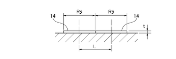
図7Aに、溶融前のハンダボール34同士の位置関係と、図7Bに溶融後の接合部14の位置関係を示す。溶融前においてハンダボール34は、間隔Lをあけて配置されている。溶融によってハンダボール34が濡れ広がり、直径がR2、厚さがtの接合部14となる。ハンダボール34同士の間隔Lを上記式で表される値とすることによって、所望の厚さtを有し、隣り合うハンダボール34同士が濡れ広がることによって接触して一体化し得る接合部14を形成することができる。すなわち、最密充填した場合に比べ、厚さtをより小さくすることができる。
なお、図6Bには、ハンダボール34をジグザグ状に配置した例を示したが、ハンダボール34を格子状、又は一直線状に配置してもよい。上記のように、所定間隔をあけて、ジグザグ状、又は格子状にハンダボール34を配置する際にも、上記バンプ形成方法を用いることができる。
上記のように電極22,24上にボールバンプを形成した後、電極22,24の表面である第1接合面を電極26,28の表面である第2接合面に向けて、上記LEDチップ12をセラミック基板16上に裏返して設置し、電極22,24と、電極26,28とがそれぞれ対応するように、LEDチップ12とセラミック基板16を位置合わせする。この状態で加熱することによって、ハンダボール34を溶融させ、冷却して凝固させることによって接合部14を形成し、電極22,24と、電極26,28を電気的に接続する。
なお、電極22,24上にボールバンプを形成した後、LEDチップ12を加熱して、ハンダボール34をリフローさせてもよい。リフローによってハンダボール34は電極22,24上に濡れ広がり、冷却することによって凝固した接合部14となる。このLEDチップ12をセラミック基板16上に裏返して設置し、電極22,24と、電極26,28とがそれぞれ対応するように、LEDチップ12とセラミック基板16を位置合わせし、加熱することによって、接合部14を再度溶融させ、冷却して凝固させることによって、電極22,24と、電極26,28を電気的に接続する。この場合、接合部14は、予め濡れ広がっているので、電極22,24と、電極26,28をより確実に接続できると共に、ボイドなどの発生をより確実に低減することができる。
(5)作用及び効果
上記のように形成されたLEDパッケージ10は、接合部14の厚さtが50μm以下でありLEDチップ12とセラミック基板16が近接していることによって、LEDチップ12で生じた熱を効率的にセラミック基板16へ伝達することができる。したがってLEDパッケージ10は、放熱性を高めることができるので、半導体発光装置11の品質を向上することができる。接合部14の厚さtは、35μm未満であるのが好ましく、20μm以下であるのがより好ましい。
上記のように形成されたLEDパッケージ10は、接合部14の厚さtが50μm以下でありLEDチップ12とセラミック基板16が近接していることによって、LEDチップ12で生じた熱を効率的にセラミック基板16へ伝達することができる。したがってLEDパッケージ10は、放熱性を高めることができるので、半導体発光装置11の品質を向上することができる。接合部14の厚さtは、35μm未満であるのが好ましく、20μm以下であるのがより好ましい。
接合部14は、ハンダボール34を用いて形成されるので、厚さtを50μm以下とすることができ、Auの使用量を低減することができる。また本実施形態の接合部14に用いられるハンダボール34は、従来のハンダペーストに比べ使用量を低減でき、また従来のシート状のろう材に比べ歩留りを向上することができる。したがってLEDパッケージ10は、Auの使用量を低減することができる。
ハンダボール34は、各枠21における塊状の前記第1相104の個数の平均が3個以下であり、表面近傍において、均一なラメラー組織が形成されているので、外観が引け巣のない良好な状態とすることができる。
ハンダボール34は、上記元素を所定の濃度範囲で含有することによって均一なラメラー組織が形成されており、外観が引け巣のない良好な状態であるので、信頼性を向上することができる。UDS法で形成することによって、均一な球径精度を有するハンダボール34を得ることができる。均一な球径精度を有するハンダボール34を用いて接合することによって、LEDパッケージ10の信頼性をより向上することができる。
ハンダボール34は、Feを含む場合のFeの濃度が10質量ppm以下、Crを含む場合のCrの濃度が100質量ppm以下、Niを含む場合のNiの濃度が5000質量ppm以下であることによって、良好な濡れ性を得ることができる。
接合部14は、ハンダが良好に濡れ広がるため、ボイドの発生を低減することができる。したがって、接合部14が電極22,24と電極26,28をより良好に電気的に接続することができるので、LEDパッケージ10は、電気伝導性、熱伝導性を高めることによって、品質をより向上することができる。このようなLEDパッケージ10は、高輝度化が必要とされる自動車用ヘッドライト等の光源に適用することができる。
2.第2実施形態
次に、本発明の第2実施形態について説明する。図8に示す接合構造体としての封止パッケージ40は、第1構造体としてのリッド(蓋)36と、第2構造体としてのベース38とを備える。リッド36は、平板状の部材であって、中央に容器部42と、容器部42を囲むように形成されたフランジ部44とを有する。容器部42は、表面を厚さ方向に凹形状に成形してなる。フランジ部44は、導電材料で形成された導電層46と、導電層46上にハンダボール34が配置されている。
次に、本発明の第2実施形態について説明する。図8に示す接合構造体としての封止パッケージ40は、第1構造体としてのリッド(蓋)36と、第2構造体としてのベース38とを備える。リッド36は、平板状の部材であって、中央に容器部42と、容器部42を囲むように形成されたフランジ部44とを有する。容器部42は、表面を厚さ方向に凹形状に成形してなる。フランジ部44は、導電材料で形成された導電層46と、導電層46上にハンダボール34が配置されている。
ベース38は、平板状の部材であって、電子デバイス48が中央に固定されており、電子デバイス48を囲むように導電材料で形成された導電層50が形成されている。電子デバイス48は、例えば、SAWフィルタ、FBARフィルタ、水晶振動子である。
第1接合面としての導電層46の表面を、第2接合面としての導電層50の表面に向けて、上記リッド36をベース38上に裏返して設置し、導電層46と導電層50とがそれぞれ対応するように、リッド36とベース38を位置合わせする。この状態で加熱することによって、ハンダボール34を溶融し、冷却して凝固させることによって接合部14を形成し、導電層46と導電層50を電気的に接続する(図9)。電子デバイス48は、容器部42とベース38表面に囲まれた空間内に密閉される。
接合部14は、厚さtが50μm以下であることによって、熱伝導性を向上できるので、品質を向上することができる。また接合部14は、上記ハンダボール34を用いて形成することによって、ボイドの発生が低減されるため、気密性を高めることができるので、封止パッケージ40の品質を向上することができると共に、上記第1実施形態と同様の効果を得ることができる。
第2実施形態の場合、リッド36に容器部42を設けた場合について説明したが、本発明はこれに限らず、ベースに容器部とフランジ部を設けてもよい。この場合、リッドは容器部が形成されていない平坦な部材であって、ベースのフランジ部に形成された導電層に対応した位置に導電層を形成したものを用いることができる。
3.第3実施形態
次に、本発明の第3実施形態について説明する。第3実施形態では、ソルダージェット法を用いてハンダボールを第1接合面に配置する接合構造体の製造方法について説明する。ソルダージェット法は、図示しないが、キャピラリー等の微小管内にハンダボールを装填し、レーザ光を照射してハンダボールを溶融すると同時に不活性ガス等で押し出し、ハンダボールを第1接合面に仮固定する方法である。ソルダージェット法によれば、フラックスを用いずに直接、第1接合面にハンダボールを仮固定することができるので、フラックス起因による不良、例えばボイドの発生や接合不良の発生を低減することができる。ソルダージェット法は、上記バンプ形成方法と組み合わせて適用してもよい。
次に、本発明の第3実施形態について説明する。第3実施形態では、ソルダージェット法を用いてハンダボールを第1接合面に配置する接合構造体の製造方法について説明する。ソルダージェット法は、図示しないが、キャピラリー等の微小管内にハンダボールを装填し、レーザ光を照射してハンダボールを溶融すると同時に不活性ガス等で押し出し、ハンダボールを第1接合面に仮固定する方法である。ソルダージェット法によれば、フラックスを用いずに直接、第1接合面にハンダボールを仮固定することができるので、フラックス起因による不良、例えばボイドの発生や接合不良の発生を低減することができる。ソルダージェット法は、上記バンプ形成方法と組み合わせて適用してもよい。
ソルダージェット法によれば、第1接合面上に1個ずつ所定間隔で仮固定されたハンダボール上にさらにハンダボールを重ねることができる。例えば、図10Aに示すように、コーナー部分において、コーナー部分の導電層46上に複数のハンダボール34を導電層46の表面に対し高さ方向に重ねた状態で仮固定することができる。ハンダボール34を複数重ねた箇所は、他の箇所に比べ、ハンダがより広い範囲に濡れ広がる。したがって複数のハンダボール34を重ねることによって、図10Bに示すように、接合部14に、拡張部60を部分的に形成することができる。
図10Bに示す接合部14は、基本接合部59と、拡張部60とを有する。基本接合部59と拡張部60は一体に形成されている。基本接合部59は、ハンダボール34を所定の間隔で高さ方向に1個ずつ配置して形成され、接合部14の長手方向(図10B中矢印A1、及びA2)に対する単位長さあたりの接合面積が一定である。基本接合部59は、幅長さが一定である。拡張部60は、前記基本接合部59より接合面積が大きい。拡張部60は、基本接合部59が折れ曲がっているコーナー部分に設けられている。
図10Bにおける破線は、拡張部60が形成されていないと仮定した場合の、基本接合部59のコーナー部分の外側縁を示す仮想線である。なお、本明細書において「一定」とは完全に一定である場合に限らず、ある程度の範囲、例えば製造上の誤差といえる範囲を含むものとする。
拡張部60は、接合部14のコーナー部分の外側縁に連続して形成されており、コーナー部分の外側へ広がる輪郭を有する。図10Bに示す輪郭は円弧状であるが、本発明はこれに限られない。コーナー部分における接合部14の内側縁から拡張部60の外側の輪郭までの長さD1は、基本接合部の幅D2よりも長い。仮想線で規定される基本接合部59は、単位長さあたりの接合面積が一定であり、フランジ部44の外側の領域まで到達していない。これに対し本変形例に係る接合部14は、拡張部60を設けたことによって接合面積が増え、フランジ部44の外側の領域まで拡張部60が十分に到達しているので、機械的強度を向上すると共に、電気伝導性、熱伝導性をより向上することができる。
図10Aは、ハンダボール34を2個重ねた場合について示したが、本発明はこれに限らず、3個以上重ねてもよい。また図10Bは、基本接合部59が直角に折れ曲がっているコーナー部分について示したが、本発明はこれに限らず、コーナー部分における基本接合部59が折れ曲がる角度は任意に選択できる。
拡張部は、コーナー部分以外の領域、例えば図11に示すように、直線部分に、一定間隔に形成してもよい。図11に示す接合部14は、直線状の基本接合部61と、基本接合部61の所定位置に拡張部62とを有する。基本接合部61と拡張部62は一体に形成されている。図11における破線は、拡張部62が形成されていないと仮定した場合の、基本接合部61の外縁を示す仮想線である。基本接合部61は、幅長さが一定であり、長手方向に対する単位長さあたりの接合面積が一定である。拡張部62は、基本接合部61の直線部分の外側縁に連続して形成されており、幅方向外側へ広がる輪郭を有する。図11に示す輪郭は円弧状であるが、本発明はこれに限られない。拡張部62の幅D3は、基本接合部61の幅D2よりも長い。本変形例に係る接合部14は、拡張部を一定間隔で設けたことによって接合面積が増え、機械的強度を向上すると共に、電気伝導性、熱伝導性をより向上することができる。
4.変形例
本発明は上記実施形態に限定されるものではなく、本発明の趣旨の範囲内で適宜変更することが可能である。例えば、第1実施形態の場合、第1構造体としてLEDチップに適用した場合について説明したが、本発明はこれに限定されず、レーザーダイオードにも適用可能である。
本発明は上記実施形態に限定されるものではなく、本発明の趣旨の範囲内で適宜変更することが可能である。例えば、第1実施形態の場合、第1構造体としてLEDチップに適用した場合について説明したが、本発明はこれに限定されず、レーザーダイオードにも適用可能である。
第1実施形態の場合、上記元素又は上記元素組合せが添加されたハンダボール34を用いて接合部14を形成した場合について説明したが、本発明はこれに限らず、上記元素又は上記元素組合せが添加されていない、Snを19質量%以上25質量%以下含有し、Auを主成分とするハンダボールを用いて接合部14を形成してもよい。
5.実施例
以下、本実施例に基づいて本発明を詳細に説明するが、これは本発明の例を示すものであり、本発明は実施例によって何ら限定されるものではない。
以下、本実施例に基づいて本発明を詳細に説明するが、これは本発明の例を示すものであり、本発明は実施例によって何ら限定されるものではない。
(サンプル)
表1に示すハンダボールを上記「(3)製造方法(ハンダボール)」で説明した手順で作製し、外観、及び濡れ性を評価した。ハンダボールの作製にあたって、まず、AuおよびSnおよび添加元素を表1の組成となるように秤量し、高周波溶解によりインゴットを作製した。インゴットをハンダ貯蔵槽に入れ、ハンダ貯蔵槽を300~400℃に加熱し、ピエゾ素子の周波数を10~50kHzに調整した。ハンダ貯蔵槽内を、N2-5体積%H2雰囲気、及び、陽圧にすることで、ハンダボールを各1万個以上作製し、任意の50個を以下の通り評価した。各ハンダボールの濃度は、ICP-MS又はICP-OESによって分析した。
表1に示すハンダボールを上記「(3)製造方法(ハンダボール)」で説明した手順で作製し、外観、及び濡れ性を評価した。ハンダボールの作製にあたって、まず、AuおよびSnおよび添加元素を表1の組成となるように秤量し、高周波溶解によりインゴットを作製した。インゴットをハンダ貯蔵槽に入れ、ハンダ貯蔵槽を300~400℃に加熱し、ピエゾ素子の周波数を10~50kHzに調整した。ハンダ貯蔵槽内を、N2-5体積%H2雰囲気、及び、陽圧にすることで、ハンダボールを各1万個以上作製し、任意の50個を以下の通り評価した。各ハンダボールの濃度は、ICP-MS又はICP-OESによって分析した。
(評価方法)
作製したハンダボールの評価は、球径精度、外観、濡れ性で評価した。球径精度は、顕微鏡を用い、X方向、Y方向の最大値を測定し、その最大値と最小値の差(公差)で評価し、公差が球径100μm以下では10μm以内、球径100μm超200μm以下では15μm以内、球径200μm超では25μm以内の場合2点、上記以外の場合を0点として評価した。その結果、作製したハンダボールは、球径40μm以上において全て上記公差内であった。
作製したハンダボールの評価は、球径精度、外観、濡れ性で評価した。球径精度は、顕微鏡を用い、X方向、Y方向の最大値を測定し、その最大値と最小値の差(公差)で評価し、公差が球径100μm以下では10μm以内、球径100μm超200μm以下では15μm以内、球径200μm超では25μm以内の場合2点、上記以外の場合を0点として評価した。その結果、作製したハンダボールは、球径40μm以上において全て上記公差内であった。
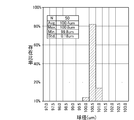
代表例として、球径50μmと、100μmのハンダボールの球径分布を、図12A、図12Bに示す。図12A、図12Bは、縦軸が存在比率、横軸が球径(μm)を示し、図12Aが球径50μmの結果、図12Bが球径100μmの結果である。球径50μmのハンダボールを作製した結果、平均球径が51.2μm、最大球径が51.5μm、最小球径が50.9μm、標準偏差が0.13μmであった。また球径100μmのハンダボールを作製した結果、平均球径が100.4μm、最大球径が100.8μm、最小球径が99.8μm、標準偏差は0.18μmであった。上記の結果から、UDS法によって、極めて高精度な球径を有するハンダボールが得られることが確認できた。
外観は、ボール表面の凹凸や引け巣を顕微鏡で観察し、凹凸及び引け巣がないものを2点、凹凸があるハンダボールが1個以上の場合1点、引け巣があるハンダボールが1個以上の場合0点として評価した。濡れ性は、銅板上にフラックスを用いずにハンダボールを置き、窒素雰囲気で320℃、1分間加熱した際に濡れ広がった面積の、元のハンダボールの投影面積に対する割合(濡れ広がり率)で評価を行い、全てのハンダボールの濡れ広がり率が、150%未満の場合0点、150%以上180%未満の場合1点、180%以上200%未満の場合2点、200%以上210%未満の場合3点、210%以上の場合4点として評価した。上記結果を表1に示す。

(評価結果)
実施例No.1~8は、接合部が、Fe、Cr、Niのうちいずれか1種の元素を含有する場合であって、ハンダボール全体に対するFeを含む場合のFeの濃度が0.1質量ppm以上10質量ppm以下であるので、凹凸及び引け巣がなく、かつ、良好な濡れ性を有するハンダボールが得られた。実施例No.1~7は、Feの濃度が0.1質量ppm以上5質量ppm以下であるので、濡れ性に関して、より優れた結果が得られた。
実施例No.1~8は、接合部が、Fe、Cr、Niのうちいずれか1種の元素を含有する場合であって、ハンダボール全体に対するFeを含む場合のFeの濃度が0.1質量ppm以上10質量ppm以下であるので、凹凸及び引け巣がなく、かつ、良好な濡れ性を有するハンダボールが得られた。実施例No.1~7は、Feの濃度が0.1質量ppm以上5質量ppm以下であるので、濡れ性に関して、より優れた結果が得られた。
実施例No.9~15は、接合部が、Fe、Cr、Niのうちいずれか1種の元素を含有する場合であって、ハンダボール全体に対するCrを含む場合のCrの濃度が0.1質量ppm以上100質量ppm以下であるので、凹凸及び引け巣がなく、かつ、良好な濡れ性を有するハンダボールが得られた。
実施例No.16~29は、接合部が、Fe、Cr、Niのうちいずれか1種の元素を含有する場合であって、ハンダボール全体に対するNiを含む場合のNiの濃度が1質量ppm以上5000質量ppm以下であるので、引け巣がなく、かつ、より優れた濡れ性を有するハンダボールが得られた。実施例No.17~21はNiの濃度が20質量ppm以上50質量ppm以下、No.24~29はNiの濃度が1000質量ppm以上5000質量ppm以下であるので、凹凸及び引け巣による外観不良がないハンダボールが得られた。実施例No.25~27は、Niの濃度が1300質量ppm以上2500質量ppm以下であるので、濡れ性に関して、さらに優れた結果が得られた。
実施例No.30~39は、接合部が、Fe、Cr、Niのうちいずれか2種以上の元素組合せを含有する場合であって、前記元素のうちFe、Crのそれぞれの濃度は、上記濃度範囲であり、Niの濃度は0質量ppm以上4990質量ppm以下の範囲であり、かつ、ハンダボール全体に対する前記元素組合せの濃度の合計が0.1質量ppm超5000質量ppm以下であるので、凹凸及び引け巣がなく、かつ、良好な濡れ性を有するハンダボールが得られた。
一方、比較例No.1、3、5は、Fe、Cr、Niのいずれも含有しないため、引け巣が発生した。比較例No.2、4はFe、Crの濃度がそれぞれ上限値を超えていたため、濡れ性が低下した。比較例No.6は、Niの濃度が上限値を超えており、均一なボールの造粒ができなかった。
10 LEDパッケージ
11 半導体発光装置(接合構造体)
12 LEDチップ(第1構造体)
14 接合部
16 セラミック基板(第2構造体)
22,24 電極
26,28 電極
34 ハンダボール
36 リッド(第1構造体)
38 ベース(第2構造体)
40 封止パッケージ(接合構造体)
42 容器部
44 フランジ部
46 導電層
48 電子デバイス
50 導電層
59 基本接合部
60 拡張部
61 基本接合部
62 拡張部
11 半導体発光装置(接合構造体)
12 LEDチップ(第1構造体)
14 接合部
16 セラミック基板(第2構造体)
22,24 電極
26,28 電極
34 ハンダボール
36 リッド(第1構造体)
38 ベース(第2構造体)
40 封止パッケージ(接合構造体)
42 容器部
44 フランジ部
46 導電層
48 電子デバイス
50 導電層
59 基本接合部
60 拡張部
61 基本接合部
62 拡張部
Claims (18)
- 第1構造体と、
Au-Sn系合金で形成された接合部を介して前記第1構造体に接合された第2構造体と、
を備えた接合構造体であって、
前記接合部の厚さが3μm以上50μm以下である、接合構造体。 - 前記接合部は、単位長さあたりの接合面積が一定である基本接合部と、前記基本接合部より単位長さあたりの接合面積が大きい拡張部とが一体に形成されている、請求項1に記載の接合構造体。
- 前記接合部は、Snを19質量%以上25質量%以下含有し、残部がAuを主成分とし、
Fe、Cr、Niのいずれか1種の元素を含有し、
前記接合部全体に対する、Feを含む場合のFeの濃度が0.1質量ppm以上10質量ppm以下であり、Crを含む場合のCrの濃度が0.1質量ppm以上100質量ppm以下であり、Niを含む場合のNiの濃度が1質量ppm以上5000質量ppm以下である、請求項1又は2に記載の接合構造体。 - 前記接合部は、Snを19質量%以上25質量%以下含有し、残部がAuを主成分とし、
Fe、Cr、Niから選ばれる少なくとも2種以上の元素組合せを含有し、
前記接合部全体に対する前記元素組合せの濃度の合計が0.1質量ppm超5000質量ppm以下であり、Feを含む場合のFeの濃度が0.1質量ppm以上10質量ppm以下であり、Crを含む場合のCrの濃度が0.1質量ppm以上100質量ppm以下であり、Niの濃度が0質量ppm以上4990質量ppm以下の範囲である、請求項1又は2に記載の接合構造体。 - 第1構造体と、
Au-Sn系合金で形成された接合部を介して前記第1構造体に接合された第2構造体と、
を備えた接合構造体の製造方法であって、
前記第1構造体の第1接合面に前記Au-Sn系合金で形成されたハンダボールを固定するボール固定工程と、
前記第1接合面を前記第2構造体の第2接合面に向けて、前記第2構造体に対して前記第1構造体を裏返して、前記第1接合面と前記第2接合面を電気的に接続する工程と、
を備え、
前記接合部の厚さが3μm以上50μm以下である、接合構造体の製造方法。 - 前記ボール固定工程は、前記ハンダボールを前記第1接合面に対し高さ方向に複数重ねて固定する多重固定工程を有する、請求項5に記載の接合構造体の製造方法。
- 前記ボール固定工程は、前記ハンダボールを最密充填で前記第1接合面に固定する請求項5又は6に記載の接合構造体の製造方法。
- 前記ハンダボールの直径をR1、前記接合部の厚さをtとした場合、前記ボール固定工程において前記ハンダボールは、下記式(1)で表される間隔Lで前記第1接合面上に配置される、請求項5又は6に記載の接合構造体の製造方法。
L=√(2R1 3/3t)・・・(1) - 前記ハンダボールは、Snを19質量%以上25質量%以下含有し、残部がAuを主成分とし、
Fe、Cr、Niのいずれか1種の元素を含有し、
前記ハンダボール全体に対する、Feを含む場合のFeの濃度が0.1質量ppm以上10質量ppm以下であり、Crを含む場合のCrの濃度が0.1質量ppm以上100質量ppm以下であり、Niを含む場合のNiの濃度が1質量ppm以上5000質量ppm以下である、請求項5又は6に記載の接合構造体の製造方法。 - 前記ハンダボールは、Snを19質量%以上25質量%以下含有し、残部がAuを主成分とし、
Fe、Cr、Niから選ばれる少なくとも2種以上の元素組合せを含有し、
前記ハンダボール全体に対する前記元素組合せの濃度の合計が0.1質量ppm超5000質量ppm以下であり、Feを含む場合のFeの濃度が0.1質量ppm以上10質量ppm以下であり、Crを含む場合のCrの濃度が0.1質量ppm以上100質量ppm以下であり、Niの濃度が0質量ppm以上4990質量ppm以下の範囲である、請求項5又は6に記載の接合構造体の製造方法。 - 前記ハンダボールは、Snを19質量%以上25質量%以下含有し、残部がAuを主成分とし、
前記ハンダボールの中央断面は、
主にAu5Snからなる第1相と主にAuSnからなる第2相とで構成されたラメラー組織を含み、
前記ハンダボールの中心を通り前記中央断面に平行な線と前記ハンダボールの外縁が交差する位置から、前記中心に向かって5μmの長さの線分を対角線として有する、前記ハンダボールの周方向に均等に4個配置された、正方形の枠内において、
前記第1相と前記第2相の間隔の2倍以上の縦横長さを有する塊状の前記第1相が、平均で3個以下である、請求項5又は6に記載の接合構造体の製造方法。 - Snを19質量%以上25質量%以下含有し、残部がAuを主成分とするハンダボールであって、
Fe、Cr、Niのいずれか1種の元素を含有し、
前記ハンダボール全体に対する、Feを含む場合のFeの濃度が0.1質量ppm以上10質量ppm以下であり、Crを含む場合のCrの濃度が0.1質量ppm以上100質量ppm以下であり、Niを含む場合のNiの濃度が1質量ppm以上5000質量ppm以下である、ハンダボール。 - Snを19質量%以上25質量%以下含有し、残部がAuを主成分とするハンダボールであって、
Fe、Cr、Niから選ばれる少なくとも2種以上の元素組合せを含有し、
前記ハンダボール全体に対する前記元素組合せの濃度の合計が0.1質量ppm超5000質量ppm以下であり、Feを含む場合のFeの濃度が0.1質量ppm以上10質量ppm以下であり、Crを含む場合のCrの濃度が0.1質量ppm以上100質量ppm以下であり、Niの濃度が0質量ppm以上4990質量ppm以下の範囲である、ハンダボール。 - 前記Feの濃度は、0.1質量ppm以上5質量ppm以下である、請求項12又は13に記載のハンダボール。
- 前記Niの濃度は、20質量ppm以上50質量ppm以下である、請求項12又は13に記載のハンダボール。
- 前記Niの濃度は、1000質量ppm以上3800質量ppm以下である、請求項12又は13に記載のハンダボール。
- 前記Niの濃度は、1300質量ppm以上2500質量ppm以下である、請求項12又は13に記載のハンダボール。
- Snを19質量%以上25質量%以下含有し、残部がAuを主成分とするハンダボールであって、
前記ハンダボールの中央断面は、
主にAu5Snからなる第1相と主にAuSnからなる第2相とで構成されたラメラー組織を含み、
前記ハンダボールの中心を通り前記中央断面に平行な線と前記ハンダボールの外縁が交差する位置から、前記中心に向かって5μmの長さの線分を対角線として有する、前記ハンダボールの周方向に均等に4個配置された、正方形の枠内において、
前記第1相と前記第2相の間隔の2倍以上の縦横長さを有する塊状の前記第1相が、平均で3個以下である、ハンダボール。
Priority Applications (2)
| Application Number | Priority Date | Filing Date | Title |
|---|---|---|---|
| US17/605,844 US12157189B2 (en) | 2019-04-22 | 2020-03-25 | Junction structure, method for manufacturing junction structure, and solder ball |
| JP2021515892A JP7502277B2 (ja) | 2019-04-22 | 2020-03-25 | 接合構造体、接合構造体の製造方法及びハンダボール |
Applications Claiming Priority (4)
| Application Number | Priority Date | Filing Date | Title |
|---|---|---|---|
| JP2019-081155 | 2019-04-22 | ||
| JP2019-081154 | 2019-04-22 | ||
| JP2019081155 | 2019-04-22 | ||
| JP2019081154 | 2019-04-22 |
Publications (1)
| Publication Number | Publication Date |
|---|---|
| WO2020217833A1 true WO2020217833A1 (ja) | 2020-10-29 |
Family
ID=72942244
Family Applications (1)
| Application Number | Title | Priority Date | Filing Date |
|---|---|---|---|
| PCT/JP2020/013428 Ceased WO2020217833A1 (ja) | 2019-04-22 | 2020-03-25 | 接合構造体、接合構造体の製造方法及びハンダボール |
Country Status (3)
| Country | Link |
|---|---|
| US (1) | US12157189B2 (ja) |
| JP (1) | JP7502277B2 (ja) |
| WO (1) | WO2020217833A1 (ja) |
Cited By (1)
| Publication number | Priority date | Publication date | Assignee | Title |
|---|---|---|---|---|
| JPWO2024203746A1 (ja) * | 2023-03-31 | 2024-10-03 |
Citations (4)
| Publication number | Priority date | Publication date | Assignee | Title |
|---|---|---|---|---|
| JP2014054653A (ja) * | 2012-09-12 | 2014-03-27 | Mitsubishi Materials Corp | Au−Sn合金含有ペースト、Au−Sn合金薄膜及びその成膜方法 |
| JP2017100176A (ja) * | 2015-12-04 | 2017-06-08 | 三菱マテリアル株式会社 | Au−Snはんだ粉末及びこの粉末を含むはんだ用ペースト |
| JP2017189793A (ja) * | 2016-04-13 | 2017-10-19 | 住友金属鉱山株式会社 | Au−Sn系はんだ合金 |
| JP2018065149A (ja) * | 2016-10-17 | 2018-04-26 | 住友金属鉱山株式会社 | Au−Sn系はんだ合金の打抜き加工の製造方法及びAu−Sn系はんだ合金の打抜き加工品 |
Family Cites Families (2)
| Publication number | Priority date | Publication date | Assignee | Title |
|---|---|---|---|---|
| JP3462392B2 (ja) | 1998-07-14 | 2003-11-05 | 田中貴金属工業株式会社 | 電子部品保護パッケージのシール用キャップの製造方法 |
| US10636761B2 (en) * | 2017-08-29 | 2020-04-28 | Electronics And Telecommunications Reearch Institute | Method of fabricating a semiconductor package |
-
2020
- 2020-03-25 JP JP2021515892A patent/JP7502277B2/ja active Active
- 2020-03-25 US US17/605,844 patent/US12157189B2/en active Active
- 2020-03-25 WO PCT/JP2020/013428 patent/WO2020217833A1/ja not_active Ceased
Patent Citations (4)
| Publication number | Priority date | Publication date | Assignee | Title |
|---|---|---|---|---|
| JP2014054653A (ja) * | 2012-09-12 | 2014-03-27 | Mitsubishi Materials Corp | Au−Sn合金含有ペースト、Au−Sn合金薄膜及びその成膜方法 |
| JP2017100176A (ja) * | 2015-12-04 | 2017-06-08 | 三菱マテリアル株式会社 | Au−Snはんだ粉末及びこの粉末を含むはんだ用ペースト |
| JP2017189793A (ja) * | 2016-04-13 | 2017-10-19 | 住友金属鉱山株式会社 | Au−Sn系はんだ合金 |
| JP2018065149A (ja) * | 2016-10-17 | 2018-04-26 | 住友金属鉱山株式会社 | Au−Sn系はんだ合金の打抜き加工の製造方法及びAu−Sn系はんだ合金の打抜き加工品 |
Cited By (3)
| Publication number | Priority date | Publication date | Assignee | Title |
|---|---|---|---|---|
| JPWO2024203746A1 (ja) * | 2023-03-31 | 2024-10-03 | ||
| WO2024203746A1 (ja) * | 2023-03-31 | 2024-10-03 | 日鉄ケミカル&マテリアル株式会社 | ハンダボール |
| JP7822518B2 (ja) | 2023-03-31 | 2026-03-02 | 日鉄ケミカル&マテリアル株式会社 | ハンダボール |
Also Published As
| Publication number | Publication date |
|---|---|
| US12157189B2 (en) | 2024-12-03 |
| US20220241903A1 (en) | 2022-08-04 |
| JPWO2020217833A1 (ja) | 2020-10-29 |
| JP7502277B2 (ja) | 2024-06-18 |
Similar Documents
| Publication | Publication Date | Title |
|---|---|---|
| CN103208435B (zh) | 使用锡焊膏进行的基板与焊件的接合方法 | |
| CN101740709B (zh) | 光半导体装置及其制造方法 | |
| US7667324B2 (en) | Systems, devices, components and methods for hermetically sealing electronic modules and packages | |
| JP2009190055A (ja) | ろう材、電子デバイス及び電子デバイスの封止方法 | |
| US12446377B2 (en) | Semiconductor device | |
| SE512906C2 (sv) | Förfarande vid lödning av ett halvledarchip samt RF-power transistor för genomförande därav | |
| CN101622706A (zh) | 气密密封用盖、电子部件容纳用封装和电子部件容纳用封装的制造方法 | |
| EP1341229A1 (en) | Method for hermetic sealing of electronic parts | |
| JP7502277B2 (ja) | 接合構造体、接合構造体の製造方法及びハンダボール | |
| JP2014029967A (ja) | 半導体装置及びその製造方法 | |
| JP6070927B2 (ja) | Au−Sn合金含有ペースト、Au−Sn合金薄膜及びその成膜方法 | |
| JP6083217B2 (ja) | Au−Sn−Bi合金粉末ペースト及びAu−Sn−Bi合金薄膜の成膜方法 | |
| US20230198223A1 (en) | Semiconductor device and method of manufacturing the semiconductor device | |
| US7842891B2 (en) | Sealing board and method for producing the same | |
| JP5077684B2 (ja) | ピン転写用Au−Sn合金はんだペースト | |
| JP7822518B2 (ja) | ハンダボール | |
| JP7318572B2 (ja) | 半導体装置及び半導体装置の製造方法 | |
| CN108550558A (zh) | 封装结构及焊接方法 | |
| CN101107705A (zh) | 密封板以及其制造方法 | |
| JP4332047B2 (ja) | 電子装置 | |
| CN118732263A (zh) | 光源模块及xr眼镜 | |
| JP2004156056A (ja) | ヒートシンクおよびこのヒートシンクを用いた半導体キャリヤならびに半導体素子用パッケージ | |
| JP6687465B2 (ja) | 水晶デバイスの製造方法 | |
| CN121726843A (zh) | 激光器组件及激光投影装置 | |
| CN113782450A (zh) | 凸点电极基板的形成方法 |
Legal Events
| Date | Code | Title | Description |
|---|---|---|---|
| 121 | Ep: the epo has been informed by wipo that ep was designated in this application |
Ref document number: 20794725 Country of ref document: EP Kind code of ref document: A1 |
|
| ENP | Entry into the national phase |
Ref document number: 2021515892 Country of ref document: JP Kind code of ref document: A |
|
| NENP | Non-entry into the national phase |
Ref country code: DE |
|
| 122 | Ep: pct application non-entry in european phase |
Ref document number: 20794725 Country of ref document: EP Kind code of ref document: A1 |