WO2020213566A1 - Conveying device - Google Patents
Conveying device Download PDFInfo
- Publication number
- WO2020213566A1 WO2020213566A1 PCT/JP2020/016291 JP2020016291W WO2020213566A1 WO 2020213566 A1 WO2020213566 A1 WO 2020213566A1 JP 2020016291 W JP2020016291 W JP 2020016291W WO 2020213566 A1 WO2020213566 A1 WO 2020213566A1
- Authority
- WO
- WIPO (PCT)
- Prior art keywords
- guide
- semiconductor chip
- probe
- guide probe
- chuck
- Prior art date
Links
Images


Classifications
-
- H—ELECTRICITY
- H01—ELECTRIC ELEMENTS
- H01L—SEMICONDUCTOR DEVICES NOT COVERED BY CLASS H10
- H01L21/00—Processes or apparatus adapted for the manufacture or treatment of semiconductor or solid state devices or of parts thereof
- H01L21/67—Apparatus specially adapted for handling semiconductor or electric solid state devices during manufacture or treatment thereof; Apparatus specially adapted for handling wafers during manufacture or treatment of semiconductor or electric solid state devices or components ; Apparatus not specifically provided for elsewhere
- H01L21/67005—Apparatus not specifically provided for elsewhere
- H01L21/67011—Apparatus for manufacture or treatment
- H01L21/67144—Apparatus for mounting on conductive members, e.g. leadframes or conductors on insulating substrates
-
- H—ELECTRICITY
- H01—ELECTRIC ELEMENTS
- H01L—SEMICONDUCTOR DEVICES NOT COVERED BY CLASS H10
- H01L21/00—Processes or apparatus adapted for the manufacture or treatment of semiconductor or solid state devices or of parts thereof
- H01L21/67—Apparatus specially adapted for handling semiconductor or electric solid state devices during manufacture or treatment thereof; Apparatus specially adapted for handling wafers during manufacture or treatment of semiconductor or electric solid state devices or components ; Apparatus not specifically provided for elsewhere
- H01L21/683—Apparatus specially adapted for handling semiconductor or electric solid state devices during manufacture or treatment thereof; Apparatus specially adapted for handling wafers during manufacture or treatment of semiconductor or electric solid state devices or components ; Apparatus not specifically provided for elsewhere for supporting or gripping
- H01L21/6838—Apparatus specially adapted for handling semiconductor or electric solid state devices during manufacture or treatment thereof; Apparatus specially adapted for handling wafers during manufacture or treatment of semiconductor or electric solid state devices or components ; Apparatus not specifically provided for elsewhere for supporting or gripping with gripping and holding devices using a vacuum; Bernoulli devices
-
- H—ELECTRICITY
- H01—ELECTRIC ELEMENTS
- H01L—SEMICONDUCTOR DEVICES NOT COVERED BY CLASS H10
- H01L21/00—Processes or apparatus adapted for the manufacture or treatment of semiconductor or solid state devices or of parts thereof
- H01L21/67—Apparatus specially adapted for handling semiconductor or electric solid state devices during manufacture or treatment thereof; Apparatus specially adapted for handling wafers during manufacture or treatment of semiconductor or electric solid state devices or components ; Apparatus not specifically provided for elsewhere
- H01L21/677—Apparatus specially adapted for handling semiconductor or electric solid state devices during manufacture or treatment thereof; Apparatus specially adapted for handling wafers during manufacture or treatment of semiconductor or electric solid state devices or components ; Apparatus not specifically provided for elsewhere for conveying, e.g. between different workstations
- H01L21/67703—Apparatus specially adapted for handling semiconductor or electric solid state devices during manufacture or treatment thereof; Apparatus specially adapted for handling wafers during manufacture or treatment of semiconductor or electric solid state devices or components ; Apparatus not specifically provided for elsewhere for conveying, e.g. between different workstations between different workstations
- H01L21/67721—Apparatus specially adapted for handling semiconductor or electric solid state devices during manufacture or treatment thereof; Apparatus specially adapted for handling wafers during manufacture or treatment of semiconductor or electric solid state devices or components ; Apparatus not specifically provided for elsewhere for conveying, e.g. between different workstations between different workstations the substrates to be conveyed not being semiconductor wafers or large planar substrates, e.g. chips, lead frames
Definitions
- the present invention relates to a transport device.
- a semiconductor chip which is a fragment of a semiconductor wafer, is a component of an electronic device.
- the process of manufacturing a semiconductor chip includes the work of moving a semiconductor wafer. Further, the manufacturing process of the electronic device includes a work of picking up a semiconductor chip and a work of arranging the semiconductor chip on a circuit board. Semiconductor wafers and semiconductor chips need to be kept clean. Therefore, it is desirable that semiconductor wafers and semiconductor chips are not directly touched in these operations.
- Patent Documents 1 to 3 disclose techniques for holding a semiconductor wafer or the like in a non-contact manner.
- Bernoulli chuck is known as a technique for holding an object in a non-contact manner. Bernoulli chuck utilizes the force generated by the flow of fluid between the chuck and the object. This force attracts the object to the chuck. The pulling force is called a holding force.
- Bernoulli Chuck does not exert any binding force on the object in the lateral direction intersecting the direction of this holding force. As a result, when the object is held by the chuck and a lateral force acts on the object, the object easily moves. As a result, it was difficult to pick up the object stably.
- the present invention provides a transport device capable of stably picking up an object.
- the transport device has a chuck portion that holds an object, which is a semiconductor chip or a semiconductor wafer, in a non-contact manner so as to face the holding surface, and a guide probe capable of contacting the side surface of the object.
- the object held by the chuck portion is provided with a guide portion that restricts the movement of the object in the lateral direction in which the guide probe intersects the direction of the normal line of the holding surface.
- the guide probe can reciprocate so that the tip of the guide probe approaches and separates from the holding surface.
- the guide probe of the guide part provided in the transport device restricts the lateral movement of the object held by the chuck.
- the guide probe can move closer to and further from the holding surface of the chuck. Then, when the object is brought close to the chuck, the guide probe moves so as to be close to the holding surface of the chuck. Therefore, the chuck can be easily brought close to the object regardless of the surrounding conditions of the object. Then, when the chuck holding the object is lifted, the guide probe moves away from the holding surface. As a result, there is a guide probe on the side of the object. Therefore, the lateral movement of the object is restricted. That is, it is possible to both limit the lateral movement of the object and lift the object. Therefore, the object can be picked up stably.
- the guide probe of the transport device has a first form in which the distance from the tip of the guide probe to the holding surface is the first distance, and a second form in which the distance from the tip of the guide probe to the holding surface is the second distance.
- the second distance may be shorter than the first distance. According to this configuration, the tip of the guide probe can reliably move back and forth with respect to the holding surface.
- the guide probe of the transfer device may extend in the direction of the normal line. According to this configuration, the configuration of the guide unit can be simplified.
- the guide portion of the transport device may have an urging force generating portion that provides the guide probe with an urging force in the direction of the normal line. According to this configuration, it is possible to reliably cause the tip of the guide probe to separate from the holding surface.
- At least two guide portions of the transfer device may be arranged along the first edge portion of the holding surface. At least two other guides may be arranged along the second edge of the holding surface. According to these configurations, the two guide portions can come into contact with the side surface of the object. As a result, the rotational movement of the object is preferably restricted. Therefore, the object can be picked up more stably.
- the guide portion of the transport device may have a first guide probe extending in a direction inclined in the direction of the normal line.
- Another guide may have a second guide probe that extends in a direction that slopes in the direction of the normal.
- the separation width between the tip of the first guide probe and the tip of the second guide probe may be larger than the separation width between the base end of the first guide probe and the base end of the second guide probe.
- the chuck portion of the transfer device may be a Bernoulli chuck. According to this configuration, the object can be reliably held in a non-contact manner.
- the object can be picked up stably.
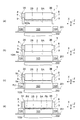
- FIG. 1 is a perspective view showing a state in which the transport device of the embodiment picks up a semiconductor chip.
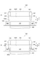
- FIG. 2 is a perspective view showing the configuration of the transport device.
- FIG. 3 is a diagram showing an end face of the transport device.
- FIG. 4 is a diagram showing an operation of picking up a semiconductor chip using the transfer device of FIG.
- FIG. 5 is a diagram showing an operation of picking up a semiconductor chip using a transfer device, following FIG. 4.
- FIG. 6 is a diagram showing a transfer device of the first modification.
- FIG. 7 is a diagram showing a transfer device of the second modification.
- FIG. 8 is a diagram showing an operation of picking up a semiconductor chip using the transport device of the comparative example.
- the diced semiconductor wafer 100 has a plurality of semiconductor chips 101.
- the distance between the semiconductor chips 101 is at least equivalent to the thickness of the dicing cutter. As an example, the distance between the semiconductor chips 101 is about 100 micrometers. It is desirable that the semiconductor chip 101 avoids contact with the chip main surface 101t in order to maintain cleanliness. Therefore, the transport device 1 of the embodiment picks up the semiconductor chips 101 one by one without touching the chip main surface 101t of the semiconductor chips 101.
- the transport device 1 can pick up the semiconductor chip 101 to be picked up even when another semiconductor chip 101 is arranged all around the semiconductor chip 101 to be picked up.
- the transport device 1 also provides the semiconductor chip 101 to be picked up even when another semiconductor chip 101 is arranged around a part of the semiconductor chip 101 to be picked up, such as the peripheral portion of the semiconductor wafer 100. Can be picked up.
- the transport device 1 for transporting the semiconductor chip 101 may be used, for example, in a die bond device and a pickup device.
- the transport device 1 has a chuck 2 (chuck portion) and a guide 3 (guide portion).
- the chuck 2 generates a holding force FK for holding the semiconductor chip 101 on the holding surface 2B.
- This holding force FK is based on, for example, the effect of Bernoulli.
- the chuck 2 is a so-called Bernoulli chuck.
- the chuck 2 has an air hole 2h. Compressed air for generating a holding force FK is supplied to the air hole 2h.
- the air hole 2h has an opening formed on the chuck main surface 2t and an opening formed on the holding surface 2B of the chuck 2.
- a control plate 4 for controlling the flow of air may be provided in the vicinity of the opening on the holding surface 2B side.
- the compressed air supplied from the chuck main surface 2t is ejected from the opening of the holding surface 2B which is the lower surface of the chuck.
- the control plate 4 controls the direction of the compressed air. As a result, the compressed air flows in the direction along the holding surface 2B. Then, the compressed air flows out from the chuck side surface 2s side to the surroundings.
- the configuration of the chuck 2 is not limited to the above configuration, and a configuration capable of holding the semiconductor chip 101 in a non-contact manner may be adopted.
- the holding force FK of the chuck 2 is along the direction of the normal line N of the holding surface 2B.
- the direction of the holding force FK is opposite to the direction of the normal N. That is, the direction of the holding force FK is toward the holding surface 2B.
- the semiconductor chip 101 is not constrained in the X direction, which is the lateral direction intersecting the normal N. Therefore, when a force in the X direction acts on the semiconductor chip 101, the semiconductor chip 101 easily moves in the X direction.
- the semiconductor chip 101 is not constrained by another lateral Y direction that intersects the normal N. Therefore, when a force in the Y direction acts on the semiconductor chip 101, the semiconductor chip 101 easily moves in the Y direction.
- the guide 3 regulates the lateral movement.
- the lateral direction includes the X direction and the Y direction.
- the transport device 1 has eight guides 3.
- two guides 3 are arranged on each chuck side surface 2s.
- the two guides 3 are arranged along the first edge 2Ba of the holding surface 2B.
- the two separate guides 3 are arranged along the second edge 2Bb of the holding surface 2B.
- the plurality of guides 3 differ only in the positions where they are arranged, and the individual configurations are the same.
- the detailed configuration of the guide 3A will be described as an example, and the description of the other guides 3 will be omitted.
- the guide 3A has a guide main body 7, a spring 8, and a guide probe 9.
- FIGS. 3, 4 and 5 show only a pair of guides 3A and 3B, and the other guides 3 are not shown.
- the guide body 7 is fixed to the chuck side surface 2s.
- the guide body 7 accommodates the spring 8 and the probe base end 9b.
- the position of the guide lower surface 7b of the guide body 7 is above the position of the holding surface 2B of the chuck 2.
- the guide lower surface 7b does not protrude from the holding surface 2B.
- the guide lower surface 7b may be flush with the holding surface 2B. Further, the guide lower surface 7b does not at least protrude from the holding force acting region SA.
- the guide probe 9 can reciprocate with respect to the guide main body 7 in the axial direction of the guide probe 9. That is, the guide probe 9 can reciprocate with respect to the chuck 2 along the normal line N of the holding surface 2B.
- the spring 8 is housed in the guide main body 7.
- the spring 8 applies an urging force FS along the normal line N to the guide probe 9.
- the spring 8 is a compression spring.
- the upper end of the spring 8 is fixed to the guide body 7.
- the lower end of the spring 8 is fixed to the guide probe 9.
- the spring 8 is slightly shorter than its natural length. According to the state slightly shorter than the natural length, in the initial state, the spring 8 applies an urging force FS that presses the guide probe 9 downward to the guide probe 9. Therefore, the guide probe 9 can be reliably projected.
- the distance from the holding surface 2B to the probe tip 9a in this state is the first distance.
- the guide probe 9 receives an upward reaction force FU.
- an upward reaction force FU acts on the guide probe 9
- the spring 8 is compressed.
- the spring 8 becomes shorter. That is, the guide probe 9 is allowed to move upward.
- the probe tip 9a is separated from the chip main surface 104t.
- the upward reaction force FU acting on the guide probe 9 disappears. Therefore, the guide probe 9 is pressed downward by the urging force FS of the spring 8.
- the guide 3 may adopt a configuration capable of exerting the urging force FS as the urging force generating unit.
- the guide 3 may use an air cylinder as an urging force generating unit. Further, the guide 3 may omit the urging force generating portion if necessary.
- the guide probe 9 can take a first form and a second form that can be switched with each other.
- the first mode is a state in which the lateral movement of the held semiconductor chip 101 can be regulated (see part (a) of FIG. 3).
- the position of the probe tip 9a of the guide probe 9 is at least below the holding force acting region SA. It suffices if the holding semiconductor chip 101 is regulated in the lateral direction. At least, the position of the probe tip 9a may be lower than the chip main surface 103t of the semiconductor chip 101 in the holding state. That is, the guide probe 9 overlaps with the chip side surface 103s of the semiconductor chip 103.
- the first form can be taken in a step of approaching the semiconductor chip 101 (for example, part (c) of FIG. 4).
- the first form can be taken in a step of holding the semiconductor chip 101 and then moving it above the semiconductor wafer 100 (for example, part (a) of FIG. 5).
- the first form does not include the moment when the chuck 2 switches from the state in which the holding force FK is not applied to the semiconductor chip 103 to the state in which the holding force FK is applied (see, for example, part (b) of FIG. 3).
- the guide probe 9 takes the second form described below.
- the second form is the state in which the guide probe 9 is most contracted.
- the distance from the probe tip 9a to the holding surface 2B is the shortest.
- the distance from the holding surface 2B to the probe tip 9a in this state is the second distance.
- the probe tip 9a overlaps the holding force acting region SA. That is, in the state where the guide probe 9 is most contracted, the position of the probe tip 9a is closer to the holding surface 2B than the lower end of the holding force acting region SA.
- the transport device 1 is moved directly above the semiconductor chip 103 to be picked up. At this time, the position of the guide probe 9 is outside the chip side surface 103s of the semiconductor chip 103.
- the transport device 1 is brought closer to the semiconductor chip 103.
- the probe tip 9a comes into contact with the chip main surface 104t of another semiconductor chip 104 adjacent to the semiconductor chip 103.
- the holding force acting region SA of the chuck 2 does not overlap with the semiconductor chip 103. Therefore, the chuck 2 cannot hold the semiconductor chip 103.
- the transport device 1 is further brought closer to the semiconductor chip 103. More specifically, the holding surface 2B is brought closer to the chip main surface 103t. Then, the probe tip 9a receives the reaction force FU from the semiconductor chip 104. Therefore, as the chuck 2 approaches the semiconductor chip 103, the spring 8 contracts. In parallel with this operation, the probe base end 9b is housed inside the guide body 7. In other words, the guide probe 9 does not move, but the chuck 2 and the guide body 7 move downward with respect to the stationary guide probe 9. Even in this state, the holding force acting region SA of the chuck 2 does not overlap with the semiconductor chip 103. Therefore, the chuck 2 cannot hold the semiconductor chip 103.
- the transport device 1 is further brought closer to the semiconductor chip 103. More specifically, the holding surface 2B is brought closer to the chip main surface 103t. As a result, the holding force acting region SA overlaps the chip main surface 103t. In this state, the holding force FK of the chuck 2 acts on the semiconductor chip 103. Then, compressed air is supplied to the chuck 2. As a result, a holding force FK is generated. Therefore, the semiconductor chip 103 is held by the chuck 2.
- the transport device 1 is separated from the dicing tape 201.
- the chuck 2 of the transport device 1 is moved upward (Z direction).
- the semiconductor chip 103 moves upward.
- the guide probe 9 keeps being pressed against the semiconductor chip 104 by the urging force FS of the spring 8. That is, the chuck 2 and the guide body 7 move upward, but the guide probe 9 keeps its position.
- the guide probe 9 housed in the guide body 7 seems to extend. Therefore, in this period, as the semiconductor chip 103 rises, an overlapping portion between the chip side surface 103s of the semiconductor chip 103 and the guide probe 9 is formed.
- the function of suppressing the lateral displacement of the semiconductor chip 103 is exhibited.
- the chip back surface 103b of the semiconductor chip 103 is peeled from the dicing tape 201, partial peeling occurs irregularly.
- an unintended external force tends to act on the semiconductor chip 103.
- the guide probe 9 already exists on the side of the semiconductor chip 103. That is, it is in a state where the lateral displacement of the semiconductor chip 103 can be suppressed.
- the semiconductor chip 103 may be pushed up by using the pickup pin 202 arranged on the back surface side of the dicing tape 201. Further, the chip main surface 103t of the semiconductor chip 103 may reach the holding force acting region SA by pushing up the pickup pin 202.
- the chuck 2 of the transport device 1 is moved upward.
- the semiconductor chip 103 moves further upward.
- the overlapping region between the chip side surface 103s and the guide probe 9 increases as described above.
- the positional relationship between the chuck 2 and the guide probe 9 returns to the first form. In this state, the length of the guide probe 9 is maximum.
- the chuck 2 of the transport device 1 is further moved upward.
- the semiconductor chip 103 moves further upward.
- the length of the guide probe 9 is the maximum. That is, the relative position of the guide probe 9 with respect to the chuck 2 does not change. Therefore, the guide probe 9 moves upward as the chuck 2 moves. As a result, the probe tip 9a is separated from the chip main surface 104t of the semiconductor chip 104.
- the transfer device 1 picks up the semiconductor chip 103.
- the transport device 1 has a chuck 2 and a guide 3.
- the chuck 2 holds the semiconductor chip 103 in a non-contact manner so as to face the holding surface 2B.
- the guide 3 has a guide probe 9 capable of contacting the chip side surface 103s of the semiconductor chip 103.
- the guide probe 9 limits the movement of the semiconductor chip 103 held by the chuck 2 in the lateral direction intersecting the direction of the normal line N of the holding surface 2B.
- the guide probe 9 can reciprocate so that the probe tip 9a approaches and separates from the holding surface 2B.
- the guide probe 9 of the guide 3 included in the transport device 1 limits the lateral movement of the semiconductor chip 103 held by the chuck 2.
- the guide probe 9 can move closer to and further from the holding surface 2B of the chuck 2.
- the guide probe 9 can move so as to be close to the holding surface 2B. Therefore, even if another semiconductor chip 104 is present around the semiconductor chip 103, the chuck 2 can be easily brought close to the semiconductor chip 103.
- the guide probe 9 moves so as to be separated from the holding surface 2B of the chuck 2.
- the guide probe 9 exists on the chip side surface 103s of the semiconductor chip 103. Therefore, the lateral movement of the semiconductor chip 103 is restricted. That is, the transport device 1 can both limit the lateral movement of the semiconductor chip 103 and lift the semiconductor chip 103. Therefore, the semiconductor chip 103 can be stably picked up.
- the guide probe 309 of the transfer device 300 of the comparative example shown in the part (a) of FIG. 8 is fixed to the guide main body 307.
- the probe tip 309a is pressed against the chip main surface 104t of another semiconductor chip 104 adjacent to the semiconductor chip 103.
- the guide probe 309 does not expand and contract. Therefore, when the chuck 302 is further brought closer to the semiconductor chip 103, the force with which the probe tip 309a presses the chip main surface 104t is further increased, as shown in the portion (b) of FIG. As a result, the semiconductor chip 104 may be damaged.
- the transfer device 1 moves so that the probe tip 9a is close to the holding surface 2B. Therefore, unlike the transfer device 300 of the comparative example, it is possible to suppress an increase in the pressing force on the chip main surface 104t with the proximity of the chuck 2. Therefore, the transport device 1 does not damage the semiconductor chip 104.
- the guide probe 9 of the transport device 1 has a first form in which the distance from the probe tip 9a to the holding surface 2B is the first distance, and a second form in which the distance from the probe tip 9a to the holding surface 2B is the second distance. , To each other.
- the second distance is shorter than the first distance. According to this configuration, the probe tip 9a can reliably move back and forth with respect to the holding surface 2B.
- the guide probe 9 of the transport device 1 extends in the direction of the normal line N. According to this configuration, the configuration of the guide 3 can be simplified.
- the guide 3 of the transport device 1 has a spring 8.
- the spring 8 provides the guide probe 9 with an urging force FS in the direction of the normal N. According to this configuration, the tip of the guide probe 9 can be reliably separated from the holding surface 2B.
- the two guides 3 of the transport device 1 are arranged along the first edge 2Ba of the holding surface 2B. At least two other guides 3 of the transport device 1 are arranged along the second edge 2Bb of the holding surface 2B. According to this configuration, the two guides 3 can come into contact with the chip side surface 103s of the semiconductor chip 103. As a result, the rotational movement of the semiconductor chip 103 is preferably restricted. Therefore, the semiconductor chip 103 can be picked up more stably.
- the transport device 1 of the present disclosure has been described above. However, the transport device 1 of the present disclosure is not limited to the above-described embodiment, and may be implemented in various forms.
- the transport device 1A shown in FIG. 6 has guides 3A and 3B.
- the guide probes 9A and 9B (first guide probe and second guide probe) of the guides 3A and 3B may be inclined with respect to the normal line N of the holding surface 2B.
- the guide probes 9A and 9B expand and contract with respect to the guide body 7 in a direction inclined with respect to the normal line N.
- the guide probes 9A and 9B may move along the direction of the normal line N. That is, the relative positional relationship of the probe tip 9a with respect to the chuck 2 may be variable.
- the spring 8 is not shown in FIG. 6, the guides 3A and 3B may or may not have the spring 8.
- the separation width H1 from the probe tip 9a of the guide probe 9A to the probe tip 9a of the guide probe 9B is larger than the separation width H2 from the probe base end 9b of the guide probe 9A to the probe base end 9b of the guide probe 9B. ..
- the separation width from the guide probe 9A to the guide probe 9B increases as the distance from the holding surface 2B increases.
- the guides 3A and 3B of the transport device 1A have guide probes 9A and 9B extending in a direction inclined in the direction of the normal line N.
- the separation width H1 from the probe tip 9a of the guide probe 9A to the probe tip 9a of the guide probe 9B is larger than the separation width H2 from the probe base end 9b of the guide probe 9A to the probe base end 9b of the guide probe 9B. According to this configuration, the semiconductor chip 103 can be picked up even when the position of the chuck 2 is displaced with respect to the semiconductor chip 103.
- the transfer device 1A can guide the semiconductor chip 103 to a predetermined holding position even if the positions of the transfer device 1A and the semiconductor chip 103 to be picked up are slightly deviated. Therefore, the condition of the position where the semiconductor chip 103 can be held can be relaxed. As a result, the transport device 1A can hold the semiconductor chip 103 more stably.
- the mechanism that allows the horizontal displacement of the semiconductor chip with respect to the transport device can be realized by a mechanism different from the mechanism shown in FIG.
- the guide probes 9C and 9D of the guides 3C and 3D have their probe side surfaces 9s inclined.
- the shapes of the guide probes 9C and 9D are recessed. Even with such a configuration, the semiconductor chip 103 can be guided to a predetermined holding position even if the position of the semiconductor chip 103 to be picked up with respect to the transfer device 1B is slightly deviated.
- the transport device 1 of the embodiment was applied to transport the semiconductor chip 103.
- the transfer device may be applied to transfer a semiconductor wafer.
Landscapes
- Engineering & Computer Science (AREA)
- Physics & Mathematics (AREA)
- Condensed Matter Physics & Semiconductors (AREA)
- General Physics & Mathematics (AREA)
- Manufacturing & Machinery (AREA)
- Computer Hardware Design (AREA)
- Microelectronics & Electronic Packaging (AREA)
- Power Engineering (AREA)
- Container, Conveyance, Adherence, Positioning, Of Wafer (AREA)
Abstract
Description
1,1A, 1B ... Conveyor device, 2 ... Chuck (chuck part), 2B ... Holding surface, 3,3A, 3B, 3C, 3D ... Guide (guide part), 4 ... Control plate, 7 ... Guide body, 8 ... Spring, 9,9A, 9B, 9C, 9D ... Guide probe, 100 ... Semiconductor wafer, 101 ... Semiconductor chip, 101, 103, 104 ... Semiconductor chip, 201 ... Dicing tape, 202 ... Pickup pin, SA ... Holding force action region , FK ... holding power, FS ... urging power, N ... normal.
Claims (7)
- 半導体チップ又は半導体ウェハである対象物を保持面に対面するように非接触で保持するチャック部と、
前記対象物の側面に当接可能なガイドプローブを有し、前記チャック部に保持された前記対象物を、前記ガイドプローブが前記保持面の法線の方向と交差する横方向への前記対象物の移動を制限するガイド部と、を備え、
前記ガイドプローブは、前記ガイドプローブの先端が前記保持面に対して近接及び離間する往復移動が可能である、搬送装置。 A chuck portion that holds an object, which is a semiconductor chip or a semiconductor wafer, in a non-contact manner so as to face the holding surface.
The object having a guide probe capable of contacting the side surface of the object, and the object held by the chuck portion in the lateral direction in which the guide probe intersects the normal direction of the holding surface. Equipped with a guide section that restricts the movement of
The guide probe is a transport device capable of reciprocating the tip of the guide probe close to and away from the holding surface. - 前記ガイドプローブは、
前記ガイドプローブの先端から前記保持面までの距離が第1距離である第1形態と、
前記ガイドプローブの先端から前記保持面までの距離が第2距離である第2形態と、を相互に切り替え、
前記第2距離は、前記第1距離よりも短い、請求項1に記載の搬送装置。 The guide probe
The first form in which the distance from the tip of the guide probe to the holding surface is the first distance,
The second form in which the distance from the tip of the guide probe to the holding surface is the second distance is switched between each other.
The transport device according to claim 1, wherein the second distance is shorter than the first distance. - 前記ガイドプローブは、前記法線の方向に延びる、請求項1に記載の搬送装置。 The transport device according to claim 1, wherein the guide probe extends in the direction of the normal.
- 前記ガイド部は、前記法線の方向に向かう付勢力を前記ガイドプローブに提供する付勢力発生部を有する、請求項1~3の何れか一項に記載の搬送装置。 The transport device according to any one of claims 1 to 3, wherein the guide unit has an urging force generating unit that provides the guide probe with an urging force in the direction of the normal line.
- 少なくとも2個の前記ガイド部は、前記保持面の第1縁部に沿って配置され、
少なくとも2個の別の前記ガイド部は、前記保持面の第2縁部に沿って配置される、請求項1~3の何れか一項に記載の搬送装置。 At least two of the guides are arranged along the first edge of the holding surface.
The transport device according to any one of claims 1 to 3, wherein at least two other guide portions are arranged along a second edge portion of the holding surface. - 前記ガイド部は、前記法線の方向に傾斜する方向に延びる第1ガイドプローブを有し、
別の前記ガイド部は、前記法線の方向に傾斜する方向に延びる第2ガイドプローブを有し、
前記第1ガイドプローブの先端と前記第2ガイドプローブの先端との離間幅は、前記第1ガイドプローブの基端と前記第2ガイドプローブの基端との離間幅よりも大きい、請求項1又は2に記載の搬送装置。 The guide portion has a first guide probe extending in a direction inclined in the direction of the normal.
Another guide portion has a second guide probe extending in a direction inclined in the direction of the normal.
The distance between the tip of the first guide probe and the tip of the second guide probe is larger than the distance between the base end of the first guide probe and the base end of the second guide probe, claim 1 or 2. The transport device according to 2. - 前記チャック部は、ベルヌーイチャックである、請求項1に記載の搬送装置。 The transport device according to claim 1, wherein the chuck portion is a Bernoulli chuck.
Priority Applications (5)
| Application Number | Priority Date | Filing Date | Title |
|---|---|---|---|
| CN202080027920.6A CN114026677A (en) | 2019-04-15 | 2020-04-13 | Conveying device |
| SG11202110943XA SG11202110943XA (en) | 2019-04-15 | 2020-04-13 | Conveying device |
| US17/603,934 US20220216089A1 (en) | 2019-04-15 | 2020-04-13 | Conveying device |
| KR1020217035723A KR20210144882A (en) | 2019-04-15 | 2020-04-13 | conveying device |
| JP2021514936A JP7161251B2 (en) | 2019-04-15 | 2020-04-13 | Conveyor |
Applications Claiming Priority (2)
| Application Number | Priority Date | Filing Date | Title |
|---|---|---|---|
| JP2019-076885 | 2019-04-15 | ||
| JP2019076885 | 2019-04-15 |
Publications (1)
| Publication Number | Publication Date |
|---|---|
| WO2020213566A1 true WO2020213566A1 (en) | 2020-10-22 |
Family
ID=72837464
Family Applications (1)
| Application Number | Title | Priority Date | Filing Date |
|---|---|---|---|
| PCT/JP2020/016291 WO2020213566A1 (en) | 2019-04-15 | 2020-04-13 | Conveying device |
Country Status (7)
| Country | Link |
|---|---|
| US (1) | US20220216089A1 (en) |
| JP (1) | JP7161251B2 (en) |
| KR (1) | KR20210144882A (en) |
| CN (1) | CN114026677A (en) |
| SG (1) | SG11202110943XA (en) |
| TW (1) | TWI747225B (en) |
| WO (1) | WO2020213566A1 (en) |
Cited By (1)
| Publication number | Priority date | Publication date | Assignee | Title |
|---|---|---|---|---|
| WO2022157830A1 (en) * | 2021-01-19 | 2022-07-28 | 株式会社新川 | Method for manufacturing semiconductor device |
Families Citing this family (1)
| Publication number | Priority date | Publication date | Assignee | Title |
|---|---|---|---|---|
| JP7418387B2 (en) | 2021-12-15 | 2024-01-19 | 矢崎総業株式会社 | Grommet and wire harness |
Citations (5)
| Publication number | Priority date | Publication date | Assignee | Title |
|---|---|---|---|---|
| JPH06321351A (en) * | 1993-05-14 | 1994-11-22 | Hiroshi Akashi | Noncontact pickup device |
| JP3122750U (en) * | 2006-04-13 | 2006-06-29 | 博 明石 | Non-contact transfer device with lifting stopper |
| JP4766824B2 (en) * | 2000-12-05 | 2011-09-07 | 日本空圧システム株式会社 | Retainer |
| KR20110125062A (en) * | 2010-05-12 | 2011-11-18 | 주식회사 에이엠에이치시스템즈 | Apparatus for aligning and pick up transporting of moving object |
| JP2012099755A (en) * | 2010-11-05 | 2012-05-24 | Disco Abrasive Syst Ltd | Transporting device |
Family Cites Families (7)
| Publication number | Priority date | Publication date | Assignee | Title |
|---|---|---|---|---|
| JP2524776B2 (en) | 1987-11-13 | 1996-08-14 | 株式会社日立製作所 | Plate transfer device |
| JP5403247B2 (en) * | 2009-09-07 | 2014-01-29 | 村田機械株式会社 | Substrate transfer device |
| JP5417467B2 (en) * | 2012-02-28 | 2014-02-12 | エルジー シーエヌエス カンパニー リミテッド | LED wafer picker |
| JP5830440B2 (en) | 2012-06-20 | 2015-12-09 | 東京エレクトロン株式会社 | Peeling system, peeling method, program, and computer storage medium |
| US9092059B2 (en) | 2012-10-26 | 2015-07-28 | Immersion Corporation | Stream-independent sound to haptic effect conversion system |
| JP2014165470A (en) | 2013-02-28 | 2014-09-08 | Nikon Corp | Conveyance system and method, exposure apparatus and method, and device manufacturing method |
| JP6948860B2 (en) * | 2017-07-14 | 2021-10-13 | 株式会社荏原製作所 | Board holding device |
-
2020
- 2020-04-01 TW TW109111322A patent/TWI747225B/en active
- 2020-04-13 WO PCT/JP2020/016291 patent/WO2020213566A1/en active Application Filing
- 2020-04-13 KR KR1020217035723A patent/KR20210144882A/en not_active Application Discontinuation
- 2020-04-13 JP JP2021514936A patent/JP7161251B2/en active Active
- 2020-04-13 SG SG11202110943XA patent/SG11202110943XA/en unknown
- 2020-04-13 US US17/603,934 patent/US20220216089A1/en active Pending
- 2020-04-13 CN CN202080027920.6A patent/CN114026677A/en active Pending
Patent Citations (5)
| Publication number | Priority date | Publication date | Assignee | Title |
|---|---|---|---|---|
| JPH06321351A (en) * | 1993-05-14 | 1994-11-22 | Hiroshi Akashi | Noncontact pickup device |
| JP4766824B2 (en) * | 2000-12-05 | 2011-09-07 | 日本空圧システム株式会社 | Retainer |
| JP3122750U (en) * | 2006-04-13 | 2006-06-29 | 博 明石 | Non-contact transfer device with lifting stopper |
| KR20110125062A (en) * | 2010-05-12 | 2011-11-18 | 주식회사 에이엠에이치시스템즈 | Apparatus for aligning and pick up transporting of moving object |
| JP2012099755A (en) * | 2010-11-05 | 2012-05-24 | Disco Abrasive Syst Ltd | Transporting device |
Cited By (3)
| Publication number | Priority date | Publication date | Assignee | Title |
|---|---|---|---|---|
| WO2022157830A1 (en) * | 2021-01-19 | 2022-07-28 | 株式会社新川 | Method for manufacturing semiconductor device |
| WO2022158166A1 (en) * | 2021-01-19 | 2022-07-28 | 株式会社新川 | Manufacturing apparatus for semiconductor device |
| TWI828355B (en) * | 2021-01-19 | 2024-01-01 | 日商新川股份有限公司 | Manufacturing apparatus of semiconductor device |
Also Published As
| Publication number | Publication date |
|---|---|
| SG11202110943XA (en) | 2021-10-28 |
| KR20210144882A (en) | 2021-11-30 |
| JPWO2020213566A1 (en) | 2020-10-22 |
| TW202040739A (en) | 2020-11-01 |
| JP7161251B2 (en) | 2022-10-26 |
| CN114026677A (en) | 2022-02-08 |
| US20220216089A1 (en) | 2022-07-07 |
| TWI747225B (en) | 2021-11-21 |
Similar Documents
| Publication | Publication Date | Title |
|---|---|---|
| WO2020213566A1 (en) | Conveying device | |
| JP2006128678A (en) | Drive mechanism for chip removing device | |
| KR102330577B1 (en) | Electronic component pickup apparatus and bonding apparatus | |
| US20010013532A1 (en) | Apparatus for positioning a thin plate | |
| JP2014011416A (en) | Pickup device and method for semiconductor chip | |
| CN110875219A (en) | Substrate bonding apparatus and substrate bonding method | |
| JP2007208088A (en) | Semiconductor manufacturing apparatus and conveyance carrier | |
| JP2007090469A (en) | Part conveying apparatus and part conveying method | |
| US20180226281A1 (en) | Pickup apparatus | |
| KR101380815B1 (en) | Die bonding device | |
| JP6563322B2 (en) | Transport device | |
| JP5075769B2 (en) | Semiconductor chip pickup device and semiconductor chip pickup method using the same | |
| JP6500357B2 (en) | Suction head, mounting device and suction method | |
| JP2004018054A (en) | Work transfer device | |
| JPH08203962A (en) | Chip positioning equipment, chip stage, and inner lead bonding equipment and method | |
| JP2014239090A (en) | Pickup system | |
| TWI732284B (en) | Transfer apparatus and transfer method for transferring light emitting diode chip | |
| JP7184006B2 (en) | Semiconductor chip pick-up jig, semiconductor chip pick-up device, and pick-up jig adjustment method | |
| JP4700639B2 (en) | Bump bonding equipment | |
| KR20230123878A (en) | Hand of industrial robot and industrial robot | |
| JP5158282B1 (en) | Conveying apparatus, semiconductor element conveying method, and semiconductor element manufacturing method | |
| JP2021100010A (en) | Pick-up device and mounting device of electronic component | |
| JP4443883B2 (en) | Chip pickup method | |
| JP2023178635A (en) | Pickup device and method of controlling pickup device | |
| CN112701078A (en) | Wafer taking and placing device |
Legal Events
| Date | Code | Title | Description |
|---|---|---|---|
| 121 | Ep: the epo has been informed by wipo that ep was designated in this application |
Ref document number: 20790805 Country of ref document: EP Kind code of ref document: A1 |
|
| DPE1 | Request for preliminary examination filed after expiration of 19th month from priority date (pct application filed from 20040101) | ||
| ENP | Entry into the national phase |
Ref document number: 2021514936 Country of ref document: JP Kind code of ref document: A |
|
| NENP | Non-entry into the national phase |
Ref country code: DE |
|
| ENP | Entry into the national phase |
Ref document number: 20217035723 Country of ref document: KR Kind code of ref document: A |
|
| 122 | Ep: pct application non-entry in european phase |
Ref document number: 20790805 Country of ref document: EP Kind code of ref document: A1 |