WO2020209109A1 - 表示装置、発光素子及び発光部材 - Google Patents
表示装置、発光素子及び発光部材 Download PDFInfo
- Publication number
- WO2020209109A1 WO2020209109A1 PCT/JP2020/014182 JP2020014182W WO2020209109A1 WO 2020209109 A1 WO2020209109 A1 WO 2020209109A1 JP 2020014182 W JP2020014182 W JP 2020014182W WO 2020209109 A1 WO2020209109 A1 WO 2020209109A1
- Authority
- WO
- WIPO (PCT)
- Prior art keywords
- light
- wavelength
- light emitting
- emitting element
- layer
- Prior art date
- Legal status (The legal status is an assumption and is not a legal conclusion. Google has not performed a legal analysis and makes no representation as to the accuracy of the status listed.)
- Ceased
Links
Images


Classifications
-
- H—ELECTRICITY
- H10—SEMICONDUCTOR DEVICES; ELECTRIC SOLID-STATE DEVICES NOT OTHERWISE PROVIDED FOR
- H10H—INORGANIC LIGHT-EMITTING SEMICONDUCTOR DEVICES HAVING POTENTIAL BARRIERS
- H10H29/00—Integrated devices, or assemblies of multiple devices, comprising at least one light-emitting semiconductor element covered by group H10H20/00
- H10H29/10—Integrated devices comprising at least one light-emitting semiconductor component covered by group H10H20/00
- H10H29/14—Integrated devices comprising at least one light-emitting semiconductor component covered by group H10H20/00 comprising multiple light-emitting semiconductor components
-
- G—PHYSICS
- G02—OPTICS
- G02B—OPTICAL ELEMENTS, SYSTEMS OR APPARATUS
- G02B5/00—Optical elements other than lenses
- G02B5/02—Diffusing elements; Afocal elements
-
- G—PHYSICS
- G02—OPTICS
- G02B—OPTICAL ELEMENTS, SYSTEMS OR APPARATUS
- G02B5/00—Optical elements other than lenses
- G02B5/20—Filters
-
- G—PHYSICS
- G09—EDUCATION; CRYPTOGRAPHY; DISPLAY; ADVERTISING; SEALS
- G09F—DISPLAYING; ADVERTISING; SIGNS; LABELS OR NAME-PLATES; SEALS
- G09F9/00—Indicating arrangements for variable information in which the information is built-up on a support by selection or combination of individual elements
- G09F9/30—Indicating arrangements for variable information in which the information is built-up on a support by selection or combination of individual elements in which the desired character or characters are formed by combining individual elements
-
- H—ELECTRICITY
- H05—ELECTRIC TECHNIQUES NOT OTHERWISE PROVIDED FOR
- H05B—ELECTRIC HEATING; ELECTRIC LIGHT SOURCES NOT OTHERWISE PROVIDED FOR; CIRCUIT ARRANGEMENTS FOR ELECTRIC LIGHT SOURCES, IN GENERAL
- H05B33/00—Electroluminescent light sources
- H05B33/02—Details
-
- H—ELECTRICITY
- H05—ELECTRIC TECHNIQUES NOT OTHERWISE PROVIDED FOR
- H05B—ELECTRIC HEATING; ELECTRIC LIGHT SOURCES NOT OTHERWISE PROVIDED FOR; CIRCUIT ARRANGEMENTS FOR ELECTRIC LIGHT SOURCES, IN GENERAL
- H05B33/00—Electroluminescent light sources
- H05B33/12—Light sources with substantially two-dimensional [2D] radiating surfaces
-
- H—ELECTRICITY
- H10—SEMICONDUCTOR DEVICES; ELECTRIC SOLID-STATE DEVICES NOT OTHERWISE PROVIDED FOR
- H10K—ORGANIC ELECTRIC SOLID-STATE DEVICES
- H10K59/00—Integrated devices, or assemblies of multiple devices, comprising at least one organic light-emitting element covered by group H10K50/00
- H10K59/30—Devices specially adapted for multicolour light emission
- H10K59/35—Devices specially adapted for multicolour light emission comprising red-green-blue [RGB] subpixels
-
- H—ELECTRICITY
- H10—SEMICONDUCTOR DEVICES; ELECTRIC SOLID-STATE DEVICES NOT OTHERWISE PROVIDED FOR
- H10K—ORGANIC ELECTRIC SOLID-STATE DEVICES
- H10K59/00—Integrated devices, or assemblies of multiple devices, comprising at least one organic light-emitting element covered by group H10K50/00
- H10K59/30—Devices specially adapted for multicolour light emission
- H10K59/38—Devices specially adapted for multicolour light emission comprising colour filters or colour changing media [CCM]
-
- H—ELECTRICITY
- H10—SEMICONDUCTOR DEVICES; ELECTRIC SOLID-STATE DEVICES NOT OTHERWISE PROVIDED FOR
- H10K—ORGANIC ELECTRIC SOLID-STATE DEVICES
- H10K59/00—Integrated devices, or assemblies of multiple devices, comprising at least one organic light-emitting element covered by group H10K50/00
- H10K59/80—Constructional details
- H10K59/875—Arrangements for extracting light from the devices
- H10K59/877—Arrangements for extracting light from the devices comprising scattering means
-
- H—ELECTRICITY
- H10—SEMICONDUCTOR DEVICES; ELECTRIC SOLID-STATE DEVICES NOT OTHERWISE PROVIDED FOR
- H10K—ORGANIC ELECTRIC SOLID-STATE DEVICES
- H10K59/00—Integrated devices, or assemblies of multiple devices, comprising at least one organic light-emitting element covered by group H10K50/00
- H10K59/80—Constructional details
- H10K59/875—Arrangements for extracting light from the devices
- H10K59/879—Arrangements for extracting light from the devices comprising refractive means, e.g. lenses
-
- H—ELECTRICITY
- H10—SEMICONDUCTOR DEVICES; ELECTRIC SOLID-STATE DEVICES NOT OTHERWISE PROVIDED FOR
- H10W—GENERIC PACKAGES, INTERCONNECTIONS, CONNECTORS OR OTHER CONSTRUCTIONAL DETAILS OF DEVICES COVERED BY CLASS H10
- H10W90/00—Package configurations
-
- H—ELECTRICITY
- H10—SEMICONDUCTOR DEVICES; ELECTRIC SOLID-STATE DEVICES NOT OTHERWISE PROVIDED FOR
- H10H—INORGANIC LIGHT-EMITTING SEMICONDUCTOR DEVICES HAVING POTENTIAL BARRIERS
- H10H20/00—Individual inorganic light-emitting semiconductor devices having potential barriers, e.g. light-emitting diodes [LED]
- H10H20/80—Constructional details
- H10H20/85—Packages
- H10H20/851—Wavelength conversion means
- H10H20/8511—Wavelength conversion means characterised by their material, e.g. binder
- H10H20/8512—Wavelength conversion materials
- H10H20/8513—Wavelength conversion materials having two or more wavelength conversion materials
-
- H—ELECTRICITY
- H10—SEMICONDUCTOR DEVICES; ELECTRIC SOLID-STATE DEVICES NOT OTHERWISE PROVIDED FOR
- H10H—INORGANIC LIGHT-EMITTING SEMICONDUCTOR DEVICES HAVING POTENTIAL BARRIERS
- H10H20/00—Individual inorganic light-emitting semiconductor devices having potential barriers, e.g. light-emitting diodes [LED]
- H10H20/80—Constructional details
- H10H20/85—Packages
- H10H20/855—Optical field-shaping means, e.g. lenses
-
- H—ELECTRICITY
- H10—SEMICONDUCTOR DEVICES; ELECTRIC SOLID-STATE DEVICES NOT OTHERWISE PROVIDED FOR
- H10H—INORGANIC LIGHT-EMITTING SEMICONDUCTOR DEVICES HAVING POTENTIAL BARRIERS
- H10H20/00—Individual inorganic light-emitting semiconductor devices having potential barriers, e.g. light-emitting diodes [LED]
- H10H20/80—Constructional details
- H10H20/882—Scattering means
-
- H—ELECTRICITY
- H10—SEMICONDUCTOR DEVICES; ELECTRIC SOLID-STATE DEVICES NOT OTHERWISE PROVIDED FOR
- H10K—ORGANIC ELECTRIC SOLID-STATE DEVICES
- H10K2102/00—Constructional details relating to the organic devices covered by this subclass
- H10K2102/301—Details of OLEDs
- H10K2102/331—Nanoparticles used in non-emissive layers, e.g. in packaging layer
-
- H—ELECTRICITY
- H10—SEMICONDUCTOR DEVICES; ELECTRIC SOLID-STATE DEVICES NOT OTHERWISE PROVIDED FOR
- H10K—ORGANIC ELECTRIC SOLID-STATE DEVICES
- H10K59/00—Integrated devices, or assemblies of multiple devices, comprising at least one organic light-emitting element covered by group H10K50/00
- H10K59/10—OLED displays
- H10K59/12—Active-matrix OLED [AMOLED] displays
-
- H—ELECTRICITY
- H10—SEMICONDUCTOR DEVICES; ELECTRIC SOLID-STATE DEVICES NOT OTHERWISE PROVIDED FOR
- H10K—ORGANIC ELECTRIC SOLID-STATE DEVICES
- H10K59/00—Integrated devices, or assemblies of multiple devices, comprising at least one organic light-emitting element covered by group H10K50/00
- H10K59/80—Constructional details
- H10K59/875—Arrangements for extracting light from the devices
- H10K59/878—Arrangements for extracting light from the devices comprising reflective means
-
- H—ELECTRICITY
- H10—SEMICONDUCTOR DEVICES; ELECTRIC SOLID-STATE DEVICES NOT OTHERWISE PROVIDED FOR
- H10K—ORGANIC ELECTRIC SOLID-STATE DEVICES
- H10K59/00—Integrated devices, or assemblies of multiple devices, comprising at least one organic light-emitting element covered by group H10K50/00
- H10K59/80—Constructional details
- H10K59/8791—Arrangements for improving contrast, e.g. preventing reflection of ambient light
- H10K59/8792—Arrangements for improving contrast, e.g. preventing reflection of ambient light comprising light absorbing layers, e.g. black layers
Definitions
- the present disclosure relates to a display device, a light emitting element, and a light emitting member.
- a liquid crystal display device equipped with a backlight composed of a blue LED and a YAG phosphor has been widely used.
- the quantum yield of the YAG phosphor is high, the emission spectrum is very wide, from 500 nm to 750 nm. Since green light and red light are extracted from such a wide range of emission spectra by a color filter, the energy utilization efficiency is low. Therefore, in order to improve energy utilization efficiency and widen the color gamut, a backlight system using a quantum dot (QD) sheet has been proposed (see, for example, Japanese Patent Publication No. 2013-544018).
- QD quantum dot
- the excitation light from the LED is color-converted for each light emitting unit (subpixel), so that the energy utilization efficiency is high.
- the tact time becomes long and the manufacturing cost increases.
- the light emitting portion provided with the quantum dots is formed based on the combination of the coating method and the photolithography technology, the light emitting portion can be formed collectively and the manufacturing cost can be reduced, but the red light emitting portion can be obtained. Since the coating method and the photolithography technique are repeated every time the green light emitting portion and the blue light emitting portion are formed to remove the quantum dots in an unnecessary region, the material utilization efficiency of the quantum dots is low and the manufacturing cost is increased.
- an object of the present disclosure is to provide a display device, a light emitting element, and a light emitting member that can achieve both improvement of light utilization efficiency and reduction of manufacturing cost.
- the display device of the present disclosure for achieving the above object is A plurality of light emitting element units including a first light emitting element, a second light emitting element, and a third light emitting element are provided.
- the first light emitting element is First light generator, which generates light with wavelength ⁇ 0 ,
- the second light emitting element is A second light generator that produces light with a wavelength of ⁇ 0 ,
- the second wavelength conversion layer having a second color conversion layer of the color conversion material thickness was comprised of particles of T 2 for color converting light having a wavelength lambda 0 which is emitted from the second optical generator unit
- T 2 the T is 3, between the average value of the average value T 2-ave and thickness of the second thickness T 2 of T 3-ave, for example, 0.9 ⁇ T 2-ave / T 3-ave ⁇ 1.1 Relationship is established, for example T 2-ave / T 3-ave ⁇ 0.9 In the case of, it is assumed that T 2 ⁇ T 3 . The same applies to the following.
- the light emitting element of the present disclosure for achieving the above object is A light generator that generates light with a wavelength of ⁇ 0 , and A wavelength conversion layer having a color conversion layer composed of color conversion material particles for color conversion of light having a wavelength ⁇ 0 emitted from a light generation unit. Is equipped with The thickness of the color conversion layer is determined based on the wavelength ⁇ "(where ⁇ "> ⁇ 0 ) of the light emitted from the wavelength conversion layer.
- the light emitting member of the present disclosure for achieving the above object is It consists of a first light emitting part, a second light emitting part and a third light emitting part.
- the first light emitting unit includes a first wavelength conversion layer having a first color conversion layer having a thickness of T 1 composed of color conversion material particles for color conversion of light having a wavelength ⁇ 0 emitted from a light generation unit.
- the second light emitting unit includes a second wavelength conversion layer having a second color conversion layer having a thickness of T 2 composed of color conversion material particles for color conversion of light having a wavelength ⁇ 0 emitted from a light generation unit.
- the third light emitting unit includes a third wavelength conversion layer having a third color conversion layer having a thickness of T 3 composed of color conversion material particles for color conversion of light having a wavelength ⁇ 0 emitted from a light generation unit. And Satisfying T 1 ⁇ T 2 ⁇ T 3 Peak wavelength ⁇ 1-peak in the optical spectrum of light emitted from the first wavelength conversion layer and peak wavelength ⁇ 2-peak in the optical spectrum of light emitted from the second wavelength conversion layer and the third wavelength conversion layer. , ⁇ 3-peak ”is different.
- FIG. 1A, 1B, and 1C are schematic partial end views of the display device and the light emitting element of the first embodiment, a diagram schematically showing the arrangement of wavelength selection layers in the display device of the first embodiment, and FIGS. It is a figure which shows typically the arrangement of the 1st electrode and the 2nd electrode in the display device of Example 1.
- FIG. 2A and 2B are schematic partial end views of the display device and the light emitting element of the first embodiment and the light emitting member of the first embodiment.
- 3A and 3B are schematic partial end views of a light generating unit and the like for explaining the manufacturing method of the display device of the first embodiment.
- 4A and 4B are schematic partial end views of a light generating unit and the like for explaining the manufacturing method of the display device of the first embodiment, following FIG.
- FIG. 5 is a schematic partial end view of a light generating unit and the like for explaining the manufacturing method of the display device of the first embodiment, following FIG. 4B.
- 6A and 6B are schematic partial end views of the display device and the light emitting element of the second embodiment and the modified example-1 of the second embodiment.
- 7A and 7B are schematic partial end views of the modified example 2 of the second embodiment and the modified example -3 of the second embodiment, respectively.
- 8A and 8B are schematic partial end view views showing a state in the middle of manufacturing the display device of the modified example-1 of the second embodiment.
- FIG. 9 is a schematic partial end view showing a state in the middle of manufacturing the display device of the modified example -1 of the second embodiment, following FIG. 8B.
- FIG. 10A and 10B are schematic partial end views of the display device and the light emitting element of the third embodiment and the modified example -1 of the third embodiment, respectively.
- 11A and 11B are schematic partial end views of the display device and the light emitting element of the second embodiment and the fourth embodiment.
- 12A and 12B are schematic partial end views of the display device and the light emitting element of the fifth embodiment and the modified example -1 of the fifth embodiment.
- FIG. 13 is a schematic partial end view of the display device and the light emitting element of the modification 2 of the fifth embodiment.
- 14A and 14B are schematic partial end views of the display device and the light emitting element of the sixth embodiment and the modified example -1 of the sixth embodiment.
- FIG. 15 is a schematic partial end view of the display device and the light emitting element of the seventh embodiment.
- 16A and 16B are schematic partial end views of the display device and the light emitting element of the eighth embodiment, and schematically show the arrangement of the side wall, the light reflecting layer, and the notch in the display device of the eighth embodiment.
- Is. 17A and 17B are schematic partial end views of the display device and the light emitting element of the ninth and tenth embodiments.
- 18A and 18B are schematic partial end views of a modified example of the display device and the light emitting element of the embodiment.
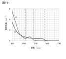
- FIG. 19 is a graph showing an example of absorption spectra of quantum dots that emit green light and quantum dots that emit red light.
- 20 is a graph showing a ray tracing simulation result of an emission spectrum when the thickness of a solution obtained by mixing quantum dots that emit green light and quantum dots that emit red light is changed.
- 21A and 21B are graphs showing the light conversion / extraction efficiency of red light, green light and blue light when the thickness of the color conversion layer is changed, and the amount of red light, the amount of green light and the amount of blue light. It is a graph which shows the ratio of the amount of light of.
- Example 1 Description of the display device, light emitting element and light emitting member of the present disclosure, and general description 2.
- Example 1 Display device, light emitting element and light emitting member 3.
- Example 2 Modification of Example 1
- Example 3 Modifications of Examples 1 and 2) 5.
- Example 4 Modifications of Examples 1 to 3) 6.
- Example 5 Modifications of Examples 1 to 4)
- Example 6 Modifications of Examples 1 to 5)
- Example 7 Modifications of Examples 1 to 6)
- Example 8 Modifications of Examples 1 to 7) 10.
- Example 9 Modifications of Examples 1 to 8) 11.
- Example 10 Modifications of Examples 1 to 9) 12.
- Other items of Examples 1 to 8 Example 9
- Example 10 Modifications of Examples 1 to 9) 12.
- the display device of the present disclosure and the light emitting member of the present disclosure may be collectively hereinafter collectively referred to as "the display device of the present disclosure, etc.”
- the light emitting element emits light as necessary. It shall be read as part.
- the color conversion material particles can be in the form of a first quantum dot and a second quantum dot. Further, the light emitting device of the present disclosure including such a preferable form may be further provided with a wavelength selection layer into which the light emitted from the wavelength conversion layer is incident.
- the color conversion material particles refer to light having a wavelength of ⁇ 0 as light having a wavelength of ⁇ 2 ”(specifically, ⁇ 2-peak ”). , ⁇ 2 "> ⁇ 0 ), and light having a wavelength ⁇ 0 is converted to light having a wavelength ⁇ 3 " (specifically, ⁇ 3-peak ”) (however, ⁇ 3 It can be in the form of a second quantum dot that converts to "> ⁇ 2 "> ⁇ 0 ). The second quantum dot further has a wavelength of ⁇ 2 ”(specifically, ⁇ 2-”.
- the relationship between the thicknesses T 1 , T 2 and T 3 is not limited, but 2 ⁇ T 2 / T 1 3 ⁇ T 3 / T 1 as well as, 1.5 ⁇ T 3 / T 2 It is desirable to satisfy 2 ⁇ T 2 / T 1 ⁇ 100 3 ⁇ T 3 / T 1 ⁇ 100 as well as, 1.5 ⁇ T 3 / T 2 ⁇ 10 It is more desirable to satisfy.
- the wavelength conversion layer further has a spacer layer.
- the total thickness of the spacer layer and the color conversion layer can be the same for each light emitting element.
- the position of the spacer layer may be the light incident side of the color conversion layer or the light emitting side of the color conversion layer.
- “Equal thickness” means that the total thickness of the spacer layer and the color conversion layer in the first light emitting element is T 1-Total , and the thickness of the spacer layer and the color conversion layer in the second light emitting element.
- T 2-Total the total thickness of the spacer layer and the color conversion layer in the third light emitting element
- 0.9 ⁇ T 1-Total / T 2-Total ⁇ 1.1 0.9 ⁇ T 2-Total / T 3-Total ⁇ 1.1 as well as, 0.9 ⁇ T 1-Total / T 3-Total ⁇ 1.1 Means to be satisfied.
- satisfying such an equation regarding the thickness may be expressed as "satisfied within the range of thickness variation ⁇ 10%".
- the material constituting the spacer layer include a transparent member, specifically, an acrylic ultraviolet curable resin, an epoxy ultraviolet curable resin, a silicone thermosetting resin, and an epoxy thermosetting resin.
- the wavelength conversion layer may be in a form containing light scattering particles, and the wavelength selection layer may include light scattering particles. It can also be in a form that includes.
- the wavelength conversion layer in each light emitting element, may be further formed to have a light scattering particle layer. In this case, the total thickness of the light scattering particle layer and the color conversion layer can be the same in each light emitting device. It is preferable that the light scattering particle layer is located on the light emitting side of the color conversion layer.
- “Equal thickness” means that the total thickness of the first light scattering particle layer and the first color conversion layer in the first light emitting element is T 1-Total ', and the second in the second light emitting element.
- the total thickness of the light scattering particle layer and the thickness of the second color conversion layer is T 2-Total ', the thickness of the third light scattering particle layer and the thickness of the third color conversion layer in the third light emitting element.
- T 3-Total ' 0.9 ⁇ T 1-Total '/ T 2-Total' ⁇ 1.1 0.9 ⁇ T 2-Total '/ T 3-Total' ⁇ 1.1 as well as, 0.9 ⁇ T 1-Total '/ T 3-Total' ⁇ 1.1 Means to be satisfied.
- Examples of the light-scattering particles and the light-scattering particles contained in the light-scattering particle layer include SiO 2 , Al 2 O 3 , and TiO 2 .
- the light emitted from the light emitting element can have a light distribution characteristic close to that of the Lambersian light distribution state or the Lambercyan light distribution state.
- each light emitting element is provided with an on-chip microlens on the light emitting side of the wavelength selection layer.
- the on-chip microlens can be an on-chip microlens having a well-known configuration and structure.
- acrylic resin, epoxy resin, polycarbonate resin (PC), polyimide resin, polymethyl methacrylate resin (PMMA), polyarylate resin (PAR), polyethylene terephthalate resin (A transparent resin material such as PET) or ABS resin, or glass can be mentioned.
- On-chip microlenses can be obtained by melt-flowing a transparent resin material, or by etching back, or with a photolithography technique using a gray tone mask. It can be obtained in combination with an etching method, or it can be obtained by a method such as forming a transparent resin material into a lens shape based on a nanoimprint method.
- the light generating unit constituting each light emitting element may be in a form connected to a drive circuit provided on the substrate.
- the drive circuit can be a drive circuit having a well-known configuration and structure for driving the light generation unit.
- a connection method between the light generator and the drive circuit provided on the substrate a method using bumps containing solder, indium, gold (Au), etc., a plating method, a method based on a chip-on-chip method, a through-chip beer ( A method using TCV) or through silicon beer (TSV), and a metal-metal bond containing Cu—Cu can be exemplified.
- the substrate include a silicon semiconductor substrate, a glass substrate, a GaN substrate, and a SiC substrate.
- a transparent material member is arranged between the light generating unit and the wavelength conversion layer.
- a transparent material member may be arranged between the wavelength conversion layer and the wavelength selection layer.
- polymethylmethacrylate polymethylmethacrylate
- PMMA polyvinyl alcohol
- PVP polyvinylphenol
- PES polyether sulfone
- PET polyethylene terephthalate
- PEN polyethylene naphthalate
- PBT polybutylene terephthalate
- acetyl cellulose tetraacetyl cellulose
- polyphenylene sulfide polycarbonate
- PC polyethylene
- PE polypropylene
- polyvinylidene fluoride brominated phenoxy, polyamide, polyimide, polystyrene
- polysulfone such as allylate and polyester sulfone
- organic polymers such as polyolefin (having a form of a polymer material such as a flexible plastic film, a plastic sheet, and a plastic substrate composed of a polymer material) are mentioned.
- the light generating unit constituting each light emitting element can be formed of a light emitting diode (LED), and in this case, the light emitting diode.
- LED light emitting diode
- the laminated illuminant structure in which the first compound semiconductor layer, the active layer and the second compound semiconductor layer are laminated includes, for example, a GaN-based compound semiconductor (including AlGaN-based compound crystal, AlGaInN mixed crystal, and GaInN mixed crystal), and an AlGaInAs-based compound semiconductor.
- the material constituting the electrode connected to the laminated light emitting body structure for driving the light generating unit examples include Pd, ITO, AuGe / NiAu laminated structure, Ti / Pt / Au laminated structure, and Ni / Au laminated structure. it can.
- the light generating unit constituting each light emitting element can be in the form of an organic electroluminescence light emitting element.
- the organic electroluminescence light emitting device (organic EL light emitting device) can be an organic EL light emitting device having a well-known structure and structure.
- the first light generation unit, the second light generation unit, and the third light generation unit that generate light having a wavelength ⁇ 0 can be light generation units having the same configuration and structure.
- an optical shutter means is provided between the wavelength conversion layer and the wavelength selection layer.
- the optical shutter means include a transmissive liquid crystal display device.
- the light emitting element unit includes not only a first light emitting element, a second light emitting element, and a third light emitting element, but also a fourth light emitting element, a fifth light emitting element, and the like. You may.
- the light emitting element and the light emitting element are separated by a side wall (bulkhead).
- the material constituting the side wall (partition wall) include resist materials, various metals, various alloys, various resins, and insulating materials such as SiO 2 and SiN.
- the side wall (bulkhead) may be in the form of surrounding each light generation unit and a connection portion connecting each light generation unit and the drive circuit.
- a light reflecting layer may be formed on the inner surface of the side wall.
- the material constituting the light reflecting layer include a multilayer film of Ag, Au, Al, or a dielectric (for example, SiO 2 , Al 2 O 3 , TiO 2 , Ta 2 O 5 ).
- the total thickness of the wavelength conversion layer and the thickness of the wavelength selection layer can be the same in each light emitting element.
- “Equal thickness” means that the total thickness of the wavelength conversion layer and the wavelength selection layer in the first light emitting element is T 1-Total ”, the thickness of the wavelength conversion layer in the second light emitting element, and the total thickness.
- an optical crosstalk suppression unit is provided in a region located between the light emitting elements and the light emitting elements.
- the spectrum of the light generated in the light generation unit may have a narrow width (that is, a single spectrum or a plurality of spectra. It may have a peak), or it may have a certain width (wide width).
- the wavelength range of wavelength ⁇ 0 can be 10 nm to 50 nm.
- the blue light specifically, for example, can be exemplified light having a wavelength range of 430nm to 500 nm (FWHM)
- the second wavelength as light of wavelength lambda 2 'emitted from the selected layer
- a green light specifically, for example, can be exemplified light having 500nm to 570nm wavelength range (FWHM)
- the third wavelength selective layer as light of wavelength lambda 3 'emitted, red light, specifically, for example, a light having a wavelength range of 610nm to 750 nm (FWHM).
- lambda 1 ' ⁇ lambda 2' ' has been defined as the wavelength ⁇ 1' ⁇ 3 a peak wavelength of a spectrum of light lambda 1-peak 'of the wavelength lambda 2' peak wavelength of the spectrum of light ⁇ 2-peak ', wavelength lambda 3' 'when a, ⁇ 1-peak' a peak wavelength of the spectrum of the light lambda 3-peak if ⁇ 2-peak ' ⁇ 3-peak', ⁇ 1 and satisfies the ' ⁇ 2' ⁇ 3 '.
- the light having a wavelength ⁇ 2 ′′ mainly emitted from the second wavelength conversion layer green light, specifically, light having a wavelength range (half-value full width) of 500 nm to 570 nm can be mentioned.
- the light having a wavelength ⁇ 3 ′′ mainly emitted from the third wavelength conversion layer red light, specifically, light having a wavelength range (half-value full width) of 610 nm to 750 nm can be mentioned.
- the bandgap energy becomes larger and the wavelength of the light emitted from the quantum dot becomes shorter. That is, the smaller the size of the quantum dot, the shorter the wavelength of light (light on the blue light side), and the larger the size of the quantum dot, the longer the light having a wavelength (red light side). Therefore, by using the same material for forming the quantum dots and adjusting the size of the quantum dots, it is possible to obtain quantum dots that emit light having a desired wavelength (color conversion to a desired color).
- the material constituting the first quantum dot and the material constituting the second quantum dot may be different materials, but the same material (however, the diameter is different) can simplify the structure.
- the quantum dots preferably have a core-shell structure.
- the first quantum dot or the second quantum dot for example, Si; Se; a calcopalite-based compound CIGS (CuInGaSe), CIS (CuInSe 2 ), CuInS 2 , CuAlS 2 , CuAlSe 2 , CuGaS 2 , CuGaSe 2 , AgAlS 2 , AgAlSe 2 , AgInS 2 , AgInSe 2 ; Perovskite-based materials; Group III-V compounds GaAs, GaP, InP, InAs, InGaAs, AlGaAs, InGaP, AlGaInP, InGaAsP, GaN; CdSe, CdSe , CdS, CdTe, In 2 Se 3 , In 2 S 3 , Bi 2 Se 3 , Bi 2 S 3 , ZnSe, ZnTe, ZnS, HgTe, HgS, PbSe, Pb
- the color conversion layer is composed of color conversion material particles, or is also composed of color conversion material particles embedded in a filler (filler, matrix).
- a filler polypropylene resin, polyethylene resin, polystyrene resin, AS resin, ABS resin, methacrylic resin, polyvinyl chloride resin, polyacetal resin, polyamide resin, polycarbonate resin, modified polyphenylene ether resin, polybutylene terephthalate resin, polyethylene Telephthalate resin, polysulfone resin, polyether sulfone resin, polyphenylene sulfide resin, polyamideimide resin, polymethylpentene resin, liquid crystal polymer resin, epoxy resin, phenol resin, urea resin, melanin resin, diallyl phthalate resin, unsaturated polyester resin, Examples thereof include a polyimide resin, a polyurethane resin, a silicone resin, an acrylic resin, or a mixture of these resins.
- the wavelength selection layer can be composed of, for example, a color filter layer made of a color resist material, and a photonic crystal or a wavelength selection element applying plasmon (a lattice-shaped hole structure in a conductor thin film). It can also be composed of a color filter layer having a provided conductor lattice structure (see, for example, Japanese Patent Application Laid-Open No. 2008-177191) and a thin film made of an inorganic material such as amorphous silicon.
- the display devices of the present disclosure include, for example, displays and monitors such as video walls, smartphones, television receivers, and personal computers, displays for AR / VR, projectors, head-up displays, head-mounted displays, and wearable devices (smart). It can be applied to various display devices such as watches).
- Example 1 relates to the display device, the light emitting element, and the light emitting member of the present disclosure.
- the relationship between the light absorption rate A in the color conversion layer, the absorption coefficient ⁇ standardized by the film thickness, and the optical path length L is shown in the following equation (1).
- the absorption coefficient ⁇ is approximately proportional to the concentration of quantum dots.
- A 1-exp (- ⁇ ⁇ L) (1)
- Quantum dot G The absorption spectra of the quantum dots that emit green light
- quantum dots that emit red light referred to as “quantum dot R” for convenience
- the quantum dot G absorbs a large amount of blue light, which is excitation light, slightly absorbs green light, and does not absorb red light.
- the quantum dot R absorbs blue light and green light, which are excitation lights, and partially absorbs red light. Due to these characteristics, when the quantum dots G and the quantum dots R are mixed, a part of the green light emitted from the quantum dots G is absorbed by the quantum dots R and converted into red light.
- the thickness of the color conversion layer increases, the components of the green light emitted from the quantum dots G that are absorbed by the quantum dots R increase, and the light is re-emitted in red. As a result, the proportion of red light increases. Further, as the thickness of the color conversion layer increases, the amount of excitation light absorbed by the quantum dots G and R increases, and the ratio of blue light emitted from the color conversion layer decreases. From the above, by controlling the thickness of the color conversion layer, it is possible to adjust the ratio of the amount of red light, the amount of green light, and the amount of blue light.
- FIG. 20 shows the ray tracing simulation result of the emission spectrum when the thickness of the solution in which the quantum dots G and the quantum dots R are mixed is changed. Further, the light conversion / extraction efficiency of red light, green light and blue light when the thickness of the color conversion layer is changed is shown in the graph of FIG. 21A, and the amount of red light, the amount of green light and the amount of blue light are shown in the graph. The ratio of is shown in the graph of FIG. 21B.
- “A” is the ray tracing simulation result of the emission spectrum when the thickness of the solution is 4.5 ⁇ m
- “B” is the ray tracing of the emission spectrum when the thickness of the solution is 6.0 ⁇ m.
- C is a ray tracing simulation result of an emission spectrum when the thickness of the solution is 10 ⁇ m
- “D” is a ray tracing simulation result of an emission spectrum when the thickness of the solution is 15 ⁇ m
- E is a ray tracing simulation result of the emission spectrum when the thickness of the solution is 18 ⁇ m.
- the peaks of the optical spectrum at a wavelength of around 540 nm in FIG. 20 partially overlap, but the highest peak has a solution thickness of 4.5 ⁇ m (“A”), and the second highest peak is.
- the solution thickness is 6.0 ⁇ m (“B”)
- the third highest peak is the solution thickness of 10 ⁇ m (“C”)
- the fourth highest peak is the solution.
- the thickness is 15 ⁇ m (“D”) and the lowest peak is the solution thickness of 18 ⁇ m (“E”). Further, the peaks of the optical spectrum at a wavelength of about 630 nm in FIG. 20 partially overlap, but the highest peaks are the solution thicknesses of 10 ⁇ m (“C”), 15 ⁇ m (“D”), and 18 ⁇ m (“E”). ”), The second highest peak is the solution thickness of 6.0 ⁇ m (“B”), and the lowest peak is the solution thickness of 4.5 ⁇ m (“A”). belongs to.
- the graph shown in FIG. 21A shows the integrated intensity obtained by integrating the light intensity of red light, the light intensity of green light, and the light intensity of blue light in the results shown in FIG. 20, and the graph shown in FIG. 21B shows the amount of red light.
- the color conversion layer of the light emitting element that emits red light, the color conversion layer of the light emitting element that emits green light, and the color conversion layer of the light emitting element that emits blue light have the same thickness, the amount of red light and green
- the manufacturing cost can be reduced.
- FIG. 1A A schematic partial end view of the display device and the light emitting element of the first embodiment is shown in FIG. 1A, the arrangement of the wavelength selection layer is schematically shown in FIG. 1B, and the arrangement of the first electrode and the second electrode is schematically shown. It is shown in FIG. 1C.
- FIG. 2A a schematic partial end view of the display device and the light emitting element of the first embodiment is shown in FIG. 2A, and a schematic partial end view of the light emitting member of the first embodiment is shown in a format different from that of FIG. 1A.
- FIG. 2B A schematic partial end view is shown in FIG. 2B. In the schematic partial end view of the display device, one light emitting element unit is shown.
- the display device of the first embodiment is A plurality of light emitting element units including a first light emitting element 10, a second light emitting element 20, and a third light emitting element 30 are provided.
- the first light emitting element 10 is First light generator 11, which generates light having a wavelength ⁇ 0
- the first wavelength conversion layer 12 has a color conversion material first color conversion layer 13 having a thickness made up of particles of T 1 to the color conversion of light having a wavelength lambda 0 which is emitted from the first light-generating unit 11 and,
- the first wavelength selection layer 14 which is incident with the light emitted from the first wavelength conversion layer 12 and emits the light having the wavelength ⁇ 1 ', Is equipped with
- the second light emitting element 20 Second light generator 21, which generates light having a wavelength ⁇ 0
- the second wavelength conversion layer 22 having a color conversion material the second color conversion layer 23 having a thickness which is composed of particles of T 2 for color converting light having a wavelength lambda 0 which is emitted from the second light
- the light emitting element of the first embodiment is Light generators 11, 21, 31 that generate light having a wavelength of ⁇ 0 , and Wavelength conversion layers 12, 22, 32 having color conversion layers 13, 23, 33 composed of color conversion material particles for color conversion of light having a wavelength ⁇ 0 emitted from light generation units 11, 21, 31.
- the thickness of the color conversion layers 12, 23, 33 is determined based on the wavelength ⁇ "(where ⁇ "> ⁇ 0 ) of the light emitted from the wavelength conversion layers 12, 22, 32.
- the light emitting member of Example 1 (also referred to as a wavelength conversion member, a wavelength conversion sheet, or a quantum dot sheet) is It is composed of a first light emitting unit 10', a second light emitting unit 20', and a third light emitting unit 30'.
- the first light emitting unit 10' has a first wavelength conversion layer 13 having a thickness T 1 composed of color conversion material particles for color conversion of light having a wavelength ⁇ 0 emitted from a light generation unit. It has layer 12 and
- the second light emitting unit 20' has a second wavelength conversion layer 23 having a thickness T 2 and is composed of color conversion material particles for color conversion of light having a wavelength ⁇ 0 emitted from a light generation unit.
- the third light emitting unit 30' has a third wavelength conversion layer 33 having a thickness T 3 and is composed of color conversion material particles for color conversion of light having a wavelength ⁇ 0 emitted from a light generation unit. It has layer 32 and Satisfying T 1 ⁇ T 2 ⁇ T 3 Peak wavelength ⁇ 1-peak in the optical spectrum of light emitted from the first wavelength conversion layer 12, and peak wavelength ⁇ 2 in the optical spectrum of light emitted from the second wavelength conversion layer 22 and the third wavelength conversion layer 32. -It is different from " peak " and ⁇ 3-peak ".
- the light emitting member of Example 1 in the light emitting member of Example 1, but not necessarily, on the first wavelength conversion layer 12, light emitted from the first wavelength conversion layer 12 is incident, emitting light having a wavelength lambda 1 '
- the first wavelength selection layer 14 is provided, and the light emitted from the second wavelength conversion layer 22 is incident on the second wavelength conversion layer 22, and the second wavelength emitting light having a wavelength ⁇ 2 '.
- a selection layer 24 is provided, and light emitted from the third wavelength conversion layer 32 is incident on the third wavelength conversion layer 32, and light having a wavelength ⁇ 3 '(however, ⁇ 1 ' ⁇ 2).
- a third wavelength selection layer 34 that emits' ⁇ 3 ') is provided.
- the light emitting member is provided on the transparent material member 73, which will be described later, but in some cases, the transparent material member 73 is unnecessary.
- the color conversion material particle is composed of a first quantum dot and a second quantum dot. Further, wavelength selection layers 14, 24, 34 to which the light emitted from the wavelength conversion layers 12, 22, 32 are incident are further provided.
- the color conversion material particles emit light having a wavelength of ⁇ 0 with a wavelength of ⁇ 2 ”(specifically, , ⁇ 2-peak ") light (but having, lambda 2" first quantum dots to be converted> into lambda 0), and, the wavelength lambda 3 "(specifically light having a wavelength lambda 0, lambda 3 It consists of a second quantum dot that converts light with -peak ") (where ⁇ 3 "> ⁇ 2 "> ⁇ 0 ).
- the second quantum dot further has a wavelength of ⁇ 2 " (specifically, ⁇ 2 "(specifically).
- T 1 ⁇ T 2 ⁇ T 3 is satisfied.
- the relationship between T 1 , T 2 and T 3 is not limited, but 2 ⁇ T 2 / T 1 3 ⁇ T 3 / T 1 as well as, 1.5 ⁇ T 3 / T 2 It is desirable to satisfy 2 ⁇ T 2 / T 1 ⁇ 100 3 ⁇ T 3 / T 1 ⁇ 100 as well as, 1.5 ⁇ T 3 / T 2 ⁇ 10 It is more desirable to satisfy.
- the total thickness of the wavelength conversion layers 12, 22, 32 (color conversion layers 13, 23, 33) and the wavelength selection layers 14, 24, 34 was set to 14 ⁇ m.
- Wavelength range of wavelength ⁇ 0 (full width at half maximum) 10 nm to 50 nm
- Wavelength range of wavelength ⁇ 1 '(full width at half maximum) 430 nm to 500 nm
- Wavelength range of wavelength ⁇ 2 '(full width at half maximum) 500 nm to 570 nm
- Wavelength range of wavelength ⁇ 3 '(full width at half maximum) 610 nm to 750 nm
- Wavelength range of wavelength ⁇ 2 ”(full width at half maximum) 500 nm to 570 nm
- Wavelength range of wavelength ⁇ 3 ”(full width at half maximum) 610 nm to 750 nm
- the wavelength conversion layers 12, 22 and 32 contain light scattering particles.
- the light scattering particles include SiO 2 , Al 2 O 3 , and TiO 2 .
- the first quantum dot (quantum dot G) and the second quantum dot (quantum dot R) are made of an InP-based semiconductor material.
- the first quantum dot is indicated by a black circle
- the second quantum dot is indicated by a circle having a hatching line drawn from the upper right to the lower left
- the light scattering particles are indicated by a white circle. Indicated by.
- the first quantum dots, the second quantum dots, and the light scattering particles are embedded in the filler (filler, matrix) 40. There is. For the sake of simplification of the drawing, it is omitted to add a hatching line to the filler 40 in the drawing.
- the first wavelength conversion layer 12, the second wavelength conversion layer 22, and the third wavelength conversion layer 32 are from the first color conversion layer 13, the second color conversion layer 23, and the third color conversion layer 33.
- the planar shape of the wavelength selection layers 14, 24, 34 is a rectangle (square or rectangle) as shown in FIG. 1B.
- the first light generation unit 11, the second light generation unit 21, and the third light generation unit 31 that generate light having a wavelength ⁇ 0 can be light generation units having the same configuration and structure.
- the light generating units 11, 21, and 31 constituting the light emitting elements 10, 20, and 30 are composed of light emitting diodes (LEDs).
- the size of the light emitting diode is not limited, but is preferably 100 ⁇ m or less.
- the light emitting diode includes at least a first compound semiconductor layer 51, an active layer (light emitting layer) 53, and a second compound semiconductor layer 52 from the wavelength conversion layer side.
- the laminated illuminant structure in which the first compound semiconductor layer 51, the active layer 53, and the second compound semiconductor layer 52 are laminated is, for example, a GaN-based compound semiconductor, specifically, an AlGaInN-based compound semiconductor having a well-known structure and structure. Consists of.
- the first electrode 55 is connected to the first compound semiconductor layer 51. Specifically, the first electrode 55 is formed on the exposed surface of the first compound semiconductor layer 51.
- the first electrode 56 is connected to the second compound semiconductor layer 52. Specifically, the second electrode 56 is formed on the exposed surface of the second compound semiconductor layer 52.
- the first compound semiconductor layer 51, the active layer 53, the second compound semiconductor layer 52, a part of the first electrode 55, and a part of the second electrode 56 are covered with an insulating layer 54 made of SiO 2 or SiN.
- a light reflecting film 57 is formed on a part of the region of the insulating layer 54.
- the first wavelength conversion layer 12 that constitutes the first light emitting element 10, the second wavelength conversion layer 22 that constitutes the second light emitting element 20, and the third wavelength conversion layer 32 that constitutes the third light emitting element 30 are side walls of each other. It is separated by (partition wall) 60. A light reflecting layer 61 is formed on the inner surface of the side wall 60.
- the first wavelength selection layer 14 mainly emits blue light from the first wavelength conversion layer 12 and allows the blue light to pass through. Finally, blue light can be emitted from the first light emitting element 10. Further, in the second light emitting element 20, based on the blue light emitted from the second light generation unit 21, mainly green light and red light are emitted from the second wavelength conversion layer 22 to pass the green light. By passing through the two-wavelength selection layer 24, green light can be finally emitted from the second light emitting element 20.
- the third light emitting element 30 based on the blue light emitted from the third light generating unit 31, the third wavelength that mainly emits red light from the third wavelength conversion layer 32 and allows the red light to pass through. By passing through the selection layer 34, red light can be finally emitted from the third light emitting element 30.
- the first compound semiconductor layer 51 (for example, the buffer layer, the n-type contact) is placed on the production substrate made of the sapphire substrate, for example, based on the MOCVD method.
- a layer (consisting of a layer and an n-type clad layer), an active layer (light emitting layer) 53, and a second compound semiconductor layer 52 (composed of, for example, a p-clad layer and a p-contact layer) are laminated.
- the manufacturing substrate is not limited to the sapphire substrate, and for example, a substrate such as a Si substrate or a GaN substrate may be used.
- the laminated illuminant structure is etched into a desired shape.
- an ohmic metal such as Pd is formed on the second compound semiconductor layer 52 based on the vapor deposition method, or a transparent conductive material layer such as ITO is formed to obtain a desired shape based on the lift-off method.
- the second electrode 56 can be formed.
- a part of the insulating layer 54 is etched to expose the first compound semiconductor layer 51, and then the exposed first compound semiconductor.
- a first electrode 55 made of Ti / Pt / Au or the like is formed on the layer 51.
- a light reflecting film 57 made of silver (Ag) or aluminum (Al) is formed on a desired region of the insulating layer 54.
- a part of the insulating layer 54 is etched to expose the second electrode 56.
- the manufacturing substrate is peeled off by using a laser lift-off (LLO) method, and the first compound semiconductor Layer 51 is exposed (see FIG. 3A).
- a side wall 60 made of a resist material (for example, a black resist material) made of a material that absorbs light is formed in a desired region on the exposed first compound semiconductor layer 51.
- the light reflecting layer 61 made of Al or Ag is formed on the entire surface by a sputtering method, and the region of the light reflecting layer 61 other than the side surface of the side wall 60 is removed by dry etching to form the light reflecting layer 61. (See Fig. 3B).
- a material in which the first quantum dot (quantum dot G), the second quantum dot (quantum dot R), and light scattering particles are dispersed in a filler made of an ultraviolet curable resin (hereinafter, "quantum dot dispersion material").
- quantum dot dispersion material In the region where the first light emitting element 10, the second light emitting element 20, and the third light emitting element 30 are to be formed, which is surrounded by the first compound semiconductor layer 51 and the light reflecting layer 61 by using a doctor blade.
- the quantum dot dispersion material is cured by irradiation with ultraviolet rays (see FIG. 4A).
- illustration of quantum dots and light scattering particles is omitted.
- the ultraviolet curable resin material 81 for nanoimprint is applied to the entire surface using a doctor blade. Then, in a state where the template is pressed against the ultraviolet curable resin material 81, the ultraviolet curable resin material 81 is cured, and then the template is removed to create a step corresponding to the thickness of the color conversion layers 13, 23, 33. It can be formed on the ultraviolet curable resin material 81 (see FIG. 4B). Next, by etching back the entire surface, the first color conversion layer 13 (thickness T 1 ) and the second color conversion having different thicknesses in the first light emitting element 10, the second light emitting element 20, and the third light emitting element 30 are performed. A layer 23 (thickness T 2 ) and a third color conversion layer 33 (thickness T 3 ) can be obtained (see FIG. 5).
- the first light emitting element 10 the second light emitting element 20, and the third light emitting element 30, the first wavelength selection layer 14, the second wavelength selection layer 24, and the third wavelength selection layer 34 are combined with the first color conversion layer 13.
- the second color conversion layer 23 and the third color conversion layer 33 are formed by a well-known method.
- the total thickness of the wavelength conversion layers 12, 22, 32 (color conversion layers 13, 23, 33) and the wavelength selection layers 14, 24, 34 is equal in each of the light emitting elements 10, 20, 30.
- a protective layer not shown
- a protective glass plate not shown
- the display device, the light emitting element, and the light emitting member of the first embodiment satisfy T 1 ⁇ T 2 ⁇ T 3 , more specifically, T 1 ⁇ T 2 ⁇ T 3 , and the first light emitting element.
- the composition of the color conversion layer constituting the second light emitting element and the third light emitting element may be the same. It is possible to improve the efficiency of light utilization as compared with the conventional technique using a YAG phosphor.
- the second light emitting element and the third light emitting element are manufactured as opposed to the conventional method in which the quantum dots G and the quantum dots R are separately painted based on the inkjet printing method or the like in order to manufacture the second light emitting element and the third light emitting element. Since it is not necessary to paint separately, it is possible to reduce the manufacturing cost and the manufacturing process. Further, since the amount of unnecessary quantum dots removed can be reduced as compared with the conventional technique, the material utilization efficiency of expensive quantum dots is high, and the manufacturing cost can also be reduced. Further, since the light generating units are individually arranged, it is possible to correspond to various pixel pitches, so that the structure is suitable for a large screen display device.
- the light emitting efficiency of the red light emitting LED and the green light emitting LED is lower than that of the blue light emitting LED.
- the light utilization efficiency can be improved by using a blue light emitting LED having a high luminous efficiency as an excitation light source and performing wavelength conversion by quantum dots having a high luminous efficiency.
- Example 2 is a modification of Example 1.
- a schematic partial end view of the display device and the light emitting element of the second embodiment is shown in FIGS. 6A and 6B.
- Example 2 The configuration and structure of the light emitting member in Example 2 or Examples 3 to 10 described later are indicated in Example 1 or Examples 3 to 10 described later, except that the light emitting member is not provided.
- the configuration and structure of the light emitting elements constituting the device can be substantially the same.
- the wavelength conversion layers 12, 22 and 32 are further made of an acrylic ultraviolet curable resin, an epoxy ultraviolet curable resin, a silicone thermosetting resin or an epoxy thermosetting resin. It has a spacer layer 70 made of The total thickness of the spacer layer 70 and the thicknesses of the color conversion layers 13, 23, 33 are equal in each of the light emitting elements 10, 20, 30.
- the position of the spacer layer 70 may be on the light emitting side of the color conversion layers 13, 23, 33 (see FIG. 6A) or on the light incident side of the color conversion layers 13, 23, 33 (FIG. 6A). See 6B).
- a schematic partial end view may not be provided with a spacer in the third light emitting element 30.
- the configuration and structure of the display device and the light emitting element of the second embodiment can be the same as the configuration and structure of the display device and the light emitting element of the first embodiment, and thus detailed description thereof will be omitted.
- a template 70 is prepared (see FIG. 8A), and the entire surface is used for nanoimprinting between [process-110] and [process-120].
- the spacer layer forming layer 70'made of the ultraviolet curable resin is applied based on the doctor blade method. Then, the template 70 "corresponds to the thickness of the color conversion layers 13, 23, 33 in each of the light emitting elements 10, 20, 30. After forming a step of thickness on the spacer layer forming layer 70'(see FIG. 8B), the spacer layer forming layer 70' is cured with ultraviolet rays to remove the template 70', thus obtaining the structure shown in FIG. After that, the steps after [Step-120] of Example 1 are executed.
- Example 1 a part of the quantum dot dispersion material filled up to the height of the side wall 60 in [Step-120] is removed by dry etching in [Step-130]. Therefore, the quantum dot dispersion material to be removed becomes a material loss.
- the filling amount of the quantum dot dispersion material can be reduced, and as a result, the material use efficiency can be improved.
- the color conversion layers 13, 23, 33 can be located farther from the light generation units 11,21,31, so that the color of heat generated in the light generation units 11,21,31 The influence on the conversion layers 13, 23 and 33 can be mitigated. Further, since the heights of the color conversion layers 13, 23, 33 which are the bases of the wavelength selection layers 14, 24, 34 can be made uniform, the coatability of the wavelength selection layers 14, 24, 34 is higher than that of the first embodiment. Is improved.
- Example 3 is a modification of Examples 1 and 2.
- a schematic partial end view of the display device and the light emitting element of the third embodiment is shown in FIGS. 10A, 10 and 11A.
- the wavelength conversion layers 12, 22 and 32 are Further, it has a light scattering particle layer 71.
- the third embodiment shown in FIG. 10A, the modified example -1 of the third embodiment shown in FIG. 10B, and the modified example 2 of the third embodiment shown in FIG. 11A are modified examples of the first embodiment.
- the total thickness of the light scattering particle layer 71 and the thicknesses of the color conversion layers 13, 23, 33 are equal in the light emitting elements 10, 20, 30.
- the light scattering particle layer 71 is located on the light emitting side of the color conversion layers 13, 23, 33.
- the light scattering particle layer 71 is formed by dispersing light scattering particles in an ultraviolet curable resin.
- FIG. 11A shows a schematic partial end view of a modified example of the display device and the light emitting element of the third embodiment, in which light scattering particles are contained in the wavelength selection layers 14, 24, and 34.
- the color conversion layers 13, 23 and 33 contain light-scattering particles. Absent. As described above, the wavelength conversion layers 12, 22 and 32 have the light scattering particle layer 71, or the wavelength selection layers 14, 24 and 34 contain the light scattering particles, so that the desired thickness is obtained.
- the filling amount of quantum dots in the color conversion layers 13, 23, and 33 having T 1 , T 2 , and T 3 can be increased. When the filling amount of the quantum dots in the color conversion layers 13, 23, 33 is small, the absorption coefficient ⁇ becomes small. In order to obtain the same light absorption rate A from the above-mentioned equation (1), it is necessary to increase the thickness of the color conversion layers 13, 23, 33.
- the thicknesses T 1 , T 2 , and T 3 can be reduced, and as a result, the thicknesses T 1 , T 2 , and T 3 can be reduced. It is possible to reduce the amount of quantum dots used.
- the configuration and structure of the display device and the light emitting element of the third embodiment can be the same as the configuration and structure of the display device and the light emitting element of the first to second embodiments. Is omitted.
- Example 4 is a modification of Examples 1 to 3.
- a schematic partial end view of the display device and the light emitting element of the fourth embodiment is shown in FIG. 11B.
- the light emitting side is closer to the light emitting side than the wavelength selection layers 14, 24, 34.
- An on-chip microlens 72 having a well-known configuration and structure is provided.
- the on-chip microlens 72 can be made of resin or glass. Specifically, for example, a flattening layer 72'is formed on the light emitting side of the wavelength selection layers 14, 24, 34, and an on-chip microlens forming layer is formed on the flattening layer 72', and the on-chip is formed.
- the -A resist layer is formed on the microlens forming layer, and the resist layer is patterned. Then, the resist layer is heated to give the resist layer a shape similar to that of the on-chip microlens, and then the resist layer and the on-chip microlens forming layer are etched back to form the on-chip microlens. Can be formed.
- the resist material can be melted by thermal reflow and the surface tension of the resist material can be used to form an on-chip microlens.
- it can be obtained by a combination of a photolithography technique using a gray tone mask and an etching method, or it can be obtained by a method such as forming a transparent resin material into a lens shape based on a nanoimprint method.
- the on-chip microlens 72 may be attached by a well-known method. Since the light from the quantum dots is emitted isotropically, when the light is emitted from the wavelength selection layers 14, 24, 34 into the air, the light distribution is in the Lambersian light distribution state or close to the Lambercyan light distribution state. Has characteristics. On the other hand, by applying the structure of the fourth embodiment to an application in which the light is desired to be concentrated at a narrow angle in front, the light utilization efficiency can be improved.
- the configuration and structure of the display device and the light emitting element of the fourth embodiment can be the same as the configuration and the structure of the display device and the light emitting element of the first to third embodiments. Is omitted.
- Example 5 is a modification of Examples 1 to 4.
- FIG. 12A shows a schematic partial end view of the display device, the light emitting element, and the light emitting member of the fifth embodiment.
- the light emitting elements 10, 20, and 30 the light generating units 11, 21, 31 and the wavelength conversion layer 12 are shown.
- PET polyethylene terephthalate
- the wavelength conversion layers 12, 22, 32 and the wavelength selection layers 14, 24, 34 are provided on the first surface 73A of the transparent material member 73, and the transparent material member facing the first surface 73A.
- the second surface 73B of 73 is adhered to the light generation units 11, 21, 31 via the adhesive layer 73'.
- the light emitting member is composed of a structure in which the first wavelength conversion layer 12, the second wavelength conversion layer 22, and the third wavelength conversion layer 32 are formed on the transparent material member 73.
- Examples of the material constituting the adhesive layer include heat-curable adhesives such as acrylic adhesives, epoxy adhesives, urethane adhesives, silicone adhesives, and cyanoacrylate adhesives, and ultraviolet curable adhesives. Can be done.
- a schematic partial end view of the modified example-1 of the fifth embodiment is a transparent material between the light generating units 11, 21, 31 and the wavelength conversion layers 12, 22, 32.
- the member 73 may be arranged, and a space (gap) 75 may be provided between the transparent material member 73 and the light generating units 11, 21, 31.
- a support portion (not shown) may be provided on the light generation portion side, and the second surface 73B of the transparent material member 73 may be attached to the support portion.
- the light generation units 11, 21, 31 and the wavelength conversion layers 12, 22, 32 (specifically, the side wall 60
- the transparent material member 74 is attached to the top surface via the adhesive layer 74'.
- a support portion is provided on the wavelength selection layer side, and the transparent material member 74 is attached to the support portion.
- the support substrate may be removed or may be left as a protective member. In this way, the light generation units 11, 21, 31 and the wavelength conversion layers 12, 22, 32 and the wavelength selection layers 14, 24, 34 (light emitting members) are separately manufactured and then bonded together, so that the manufacturing yield can be increased. It can be improved.
- a space (gap) 75 may be left between the wavelength conversion layers 12, 22, 32 and the wavelength selection layers 14, 24, 34 (specifically, the transparent material member 74) and bonded. ..
- a space (gap) 75 By providing the space (gap) 75 in this way, a part of the light from the wavelength conversion layers 12, 22 and 32 is totally reflected on the surface exposed to the space of the wavelength conversion layers 12, 22 and 32.
- Light emitted from the wavelength selection layers 14, 24, 34 is less likely to be totally reflected by a protective member (for example, a protective glass plate) arranged on the wavelength selection layers 14, 24, 34. , Light extraction efficiency is improved.
- the configuration and structure of the display device and the light emitting element of the fifth embodiment can be the same as the configuration and structure of the display device and the light emitting element of the first to fourth embodiments. Is omitted.
- Example 6 is a modification of Examples 1 to 5.
- the light generating units 11, 21, and 31 constituting the light emitting elements 10, 20, and 30 are driven by the base 90. It is connected to a circuit (not shown).
- the drive circuits provided on the light generators 11, 21, 31 and the substrate 90 are a method using bumps containing solder, indium, gold (Au), etc., a method based on a chip-on-chip method, and a through-chip beer (through chip beer).
- a method using TCV) or through silicon beer (TSV), and a metal-metal bond containing Cu—Cu can be exemplified.
- the substrate examples include a silicon semiconductor substrate, a glass substrate, a GaN substrate, and a SiC substrate.
- the drive circuit is composed of a CMOS circuit or the like provided on the substrate 90 made of a silicon semiconductor substrate, or a TFT circuit or the like provided on the substrate 90 made of a glass substrate.
- Connection portions 93, 94 connected to a drive circuit are provided on the surface of the substrate 90, and the connection portions 93, 94 are formed by, for example, first electrodes 55, 2 via bumps 91, 92 made of gold bumps. It is connected to the electrode 56.
- the display device can be miniaturized by integrating the light emitting elements 10, 20, and 30 with the drive circuit. Further, as shown in FIG.
- the configuration and structure of the display device and the light emitting element of the sixth embodiment can be the same as the configuration and the structure of the display device and the light emitting element of the first to fifth embodiments. Is omitted.
- Example 7 is a modification of Examples 1 to 6.
- the shutter means 95 is arranged.
- Specific examples of the optical shutter means 95 include a transmissive liquid crystal display device. By disposing the optical shutter means 95, it is possible to display a higher image quality and high contrast image, and it is possible to block external light when the display device is in a non-light emitting state, so that the external light contrast is improved. Can be made to.
- the light shutter means 95 may be operated in conjunction with the operation of the light generation units 11, 21, and 31.
- the configuration and structure of the display device and the light emitting element of the seventh embodiment can be the same as the configuration and structure of the display device and the light emitting element of the first to sixth embodiments. Is omitted.
- Example 8 is a modification of Examples 1 to 7.
- the first compound semiconductor layer 51 in the light generation units 11, 21, 31 is connected to the adjacent light generation unit. Therefore, the light generated by the light generation units 11, 21, 31 and the light emitted from the color conversion layers 13, 23, 33 propagate to the adjacent light emitting element through the first compound semiconductor layer 51, thereby extracting the light. There is a risk of reduced efficiency and optical crosstalk. Therefore, as shown in FIG. 16A and a schematic arrangement of the side wall 60, the light reflecting layer 61, and the notch 58 in FIG. 16B, the display device of the eighth embodiment has a schematic partial end view.
- a notch 58 is provided in which a part of the first compound semiconductor layer 51 is cut out in the boundary region between the light emitting element and the light emitting element or a region in the vicinity thereof.
- hatch lines are attached to the side wall 60, the light reflecting layer 61, and the notch 58 in order to clarify them.
- Wavelength conversion layers 12, 22, and 32 extend in the notch 58. Even if the notch 58 is provided, the current injection into the first compound semiconductor layer 51 is not hindered.
- the bottom portion of the side wall (bulkhead) 60 extends in the boundary region between the light emitting element and the light emitting element.
- the configuration and structure of the display device and the light emitting element of the eighth embodiment can be the same as the configuration and the structure of the display device and the light emitting element of the first to seventh embodiments. Is omitted.
- Example 9 is a modification of Examples 1 to 8.
- the light generating units 11', 21', and 31'that constitute each light emitting element have a well-known structure and configuration. It is composed of an organic electroluminescence light emitting device (organic EL light emitting device) having the above.
- the light generation units 11', 21', 31' are provided on a substrate 90 provided with a drive circuit (not shown) for driving the light generation units 11', 21', 31', and the insulating film 96.
- the wavelength conversion layers 12, 22, and 32 are formed on the insulating film 96.
- the light generators 11', 21', 31' emit blue light.
- the configuration and structure of the display device and the light emitting element of the ninth embodiment can be the same as the configuration and the structure of the display device and the light emitting element of the first to eighth embodiments. Is omitted.
- Example 10 is a modification of Examples 1 to 9.
- a schematic partial end view shows, in the display device of the tenth embodiment, in each light emitting element, the color conversion material particles are composed of a first quantum dot and a second quantum dot.
- T 1 1 ⁇ m
- the first light emitting element 10 the first wavelength selection that mainly emits blue light from the first wavelength conversion layer 12 and allows the blue light to pass based on the blue light emitted from the first light generation unit 11. By passing through the layer 14, blue light can be finally emitted from the first light emitting element 10. Further, in the second light emitting element 20, based on the blue light emitted from the second light generation unit 21, mainly green light and red light are emitted from the second wavelength conversion layer 22 to pass the green light.
- green light can be finally emitted from the second light emitting element 20.
- the third light emitting element 30 based on the blue light emitted from the third light generating unit 31, green light and red light are mainly emitted from the third wavelength conversion layer 32 and passed through the red light.
- red light can be finally emitted from the third light emitting element 30.
- the configuration and structure of the display device and the light emitting element of the tenth embodiment can be the same as the configuration and the structure of the display device and the light emitting element of the first to ninth embodiments. Is omitted.
- the present disclosure has been described above based on preferred examples, the present disclosure is not limited to these examples.
- Structure, connection between the light generating units 11, 21, 31 and the drive circuit is an example, and can be changed as appropriate.
- the planar shapes of the wavelength selection layers 14, 24, and 34 are rectangular (square or rectangular), but the present invention is not limited to this, and circular, elliptical, oval, and so on. It can be a polygon (for example, a hexagon).
- the arrangement of the light emitting elements is essentially arbitrary, and may be a stripe arrangement, a diagonal arrangement, a delta arrangement, a rectangle arrangement, or a Bayer arrangement.
- the sizes of the first light emitting element, the second light emitting element, and the third light emitting element (the area of the light emitting region of the light emitting element) may be changed.
- the side wall (partition wall) 60 is said to be upright with respect to the light generating portions 11, 21, 31 but is not limited to this, as shown in FIG. 18A as a schematic partial end view.
- the wavelength conversion layer 12, 22, 32 may be tapered from the bottom to the top, or as shown in FIG. 18B as a schematic partial end view, from the bottom of the wavelength conversion layers 12, 22, 32. It may be curved (bowl-shaped) that spreads over the top. In this case, the planar shapes of the wavelength selection layers 14, 24, and 34 are circular. Then, by adopting these shapes, it is possible to increase the front luminance of the display device.
- the present disclosure may also have the following configuration.
- a plurality of light emitting element units including a first light emitting element, a second light emitting element, and a third light emitting element are provided.
- the first light emitting element is First light generator, which generates light with wavelength ⁇ 0 ,
- the second light emitting element is A second light generator that produces light with a wavelength of ⁇ 0 ,
- the second wavelength conversion layer having a second color conversion layer of the color conversion material thickness was comprised of particles of T 2 for color converting light having a wavelength lambda 0 which is emitted from the second optical generator unit, and
- the color conversion material particles are the first quantum dot that converts light having a wavelength ⁇ 0 into light having a wavelength ⁇ 2 ”(where ⁇ 2 “> ⁇ 0 ), and a wavelength.
- the display device according to [A02], wherein the second quantum dot further converts light having a wavelength ⁇ 2 "into light having a wavelength ⁇ 3 ".
- the wavelength conversion layer further has a spacer layer.
- the spacer layer is located on the light incident side of the color conversion layer.
- [A08] The display device according to [A06], wherein the spacer layer is located on the light emitting side of the color conversion layer.
- [A09] The display device according to any one of [A01] to [A08], wherein the wavelength conversion layer contains light-scattering particles in each light emitting device.
- the wavelength selection layer contains light scattering particles in each light emitting element.
- [A11] The display device according to any one of [A01] to [A10], wherein the wavelength conversion layer in each light emitting element further has a light scattering particle layer.
- [A12] The display device according to [A11], wherein the total thickness of the light scattering particle layer and the color conversion layer is the same for each light emitting element.
- [A13] The display device according to any one of [A01] to [A12], wherein each light emitting element is provided with an on-chip microlens on the light emitting side of the wavelength selection layer.
- [A14] The display device according to any one of [A01] to [A13], wherein the light generating unit constituting each light emitting element is connected to a drive circuit provided on the substrate.
- [A15] The display device according to any one of [A01] to [A14], wherein a transparent material member is arranged between the light generating unit and the wavelength conversion layer in each light emitting element.
- [A16] The display device according to any one of [A01] to [A14], wherein a transparent material member is arranged between the wavelength conversion layer and the wavelength selection layer in each light emitting element.
- [A17] The display device according to [A15] or [A16], wherein a space (gap) is provided on the light generating portion side of the transparent material member.
- [A18] The display device according to [A17], wherein a space (gap) is provided between the wavelength conversion layer and the wavelength selection layer.
- [A19] The display device according to [A17], wherein a space (gap) is provided between the light generation unit and the wavelength conversion layer.
- [A20] The display device according to [A15], wherein the first wavelength conversion layer, the second wavelength conversion layer, and the third wavelength conversion layer are formed on a transparent material member.
- [A21] The display device according to any one of [A01] to [A20], wherein the light generating unit constituting each light emitting element is composed of a light emitting diode.
- an optical shutter means is provided between the wavelength conversion layer and the wavelength selection layer in each light emitting element.
- the display device according to [A23], wherein the optical shutter means comprises a transmissive liquid crystal display device.
- A27 The display device according to [A25], wherein in each light emitting element, the light generating unit and the wavelength conversion layer are surrounded by a side wall (bulkhead).
- [A28] The display device according to any one of [A25] to [A27], wherein a light reflecting layer is formed on the inner surface of the side wall.
- [A29] The display device according to any one of [A01] to [A28], wherein the thickness of the wavelength conversion layer and the total thickness of the wavelength selection layer are equal in each light emitting element.
- [A30] The display device according to any one of [A01] to [A29], wherein an optical crosstalk suppression unit is provided in a region located between the light emitting elements.
- the color conversion layer is composed of color conversion material particles embedded in a filler.
- ⁇ Light emitting element >> A light generator that generates light with a wavelength of ⁇ 0 , and A wavelength conversion layer having a color conversion layer composed of color conversion material particles for color conversion of light having a wavelength ⁇ 0 emitted from a light generation unit. Is equipped with The thickness of the color conversion layer is a light emitting element determined based on the wavelength ⁇ "(where ⁇ "> ⁇ 0 ) of the light emitted from the wavelength conversion layer.
- the light emitting device according to [B01] wherein the color conversion material particles are composed of quantum dots.
- the first light emitting unit includes a first wavelength conversion layer having a first color conversion layer having a thickness of T 1 composed of color conversion material particles for color conversion of light having a wavelength ⁇ 0 emitted from a light generation unit.
- the second light emitting unit includes a second wavelength conversion layer having a second color conversion layer having a thickness of T 2 composed of color conversion material particles for color conversion of light having a wavelength ⁇ 0 emitted from a light generation unit.
- the third light emitting unit includes a third wavelength conversion layer having a third color conversion layer having a thickness of T 3 composed of color conversion material particles for color conversion of light having a wavelength ⁇ 0 emitted from a light generation unit. And Satisfying T 1 ⁇ T 2 ⁇ T 3 A light emitting member whose peak wavelength in the optical spectrum of light emitted from the first wavelength conversion layer is different from the peak wavelength in the optical spectrum of light emitted from the second wavelength conversion layer and the third wavelength conversion layer. [C02] In each light emitting unit, the color conversion material particles convert light having a wavelength ⁇ 0 into light having a wavelength ⁇ 2 ”(where ⁇ 2 “> ⁇ 0 ), and a first quantum dot and a wavelength.
- [C04] The light emitting member according to [C02] or [C03], which satisfies T 1 ⁇ T 2 T 3 .
- [C05] The light emitting member according to [C02] or [C03] that satisfies T 1 ⁇ T 2 ⁇ T 3 .
- the wavelength conversion layer further has a spacer layer.
- [C07] The light emitting member according to [C06], wherein the spacer layer is located on the light incident side of the color conversion layer.
- the light emitting member according to [C06], wherein the [C08] spacer layer is located on the light emitting side of the color conversion layer.
- [C10] The light emitting member according to any one of [C01] to [C09], wherein the wavelength conversion layer further has a light scattering particle layer in each light emitting unit.
- [C11] The light emitting member according to [C10], wherein the thickness of the light scattering particle layer and the total thickness of the color conversion layer are equal in each light emitting portion.
- [C12] The light emitting member according to any one of [C01] to [C11], wherein a wavelength selection layer is arranged on the light emitting side of each light emitting unit on the light emitting side of the wavelength conversion layer.
- [C13] The light emitting member according to [C12], wherein light scattering particles are contained in the wavelength selection layer in each light emitting unit.
- [C14] The light emitting member according to [C12] or [C13], wherein a transparent material member is arranged between the wavelength conversion layer and the wavelength selection layer in each light emitting unit.
- [C15] The light emitting member according to [C14], wherein a space (gap) is provided on the light generating portion side of the transparent material member.
- [C16] The light emitting member according to any one of [C01] to [C13], wherein the wavelength conversion layer is provided on the transparent material member in each light emitting unit.
- [C17] The light emitting member according to any one of [C01] to [C16], wherein an optical shutter means is arranged between the wavelength conversion layer and the wavelength selection layer in each light emitting unit.
- [C18] The light emitting member according to [C17], wherein the light shutter means comprises a transmissive liquid crystal display device.
- [C19] The light emitting unit according to any one of [C01] to [C18], wherein the light emitting unit and the light emitting unit are separated by a side wall (partition wall).
- [C20] The light emitting member according to [C19], wherein the wavelength conversion layer is surrounded by a side wall (bulkhead) in each light emitting portion.
- [C21] The light emitting member according to [C19] or [C20], wherein a light reflecting layer is formed on the inner surface of the side wall.
- [C22] The light emitting member according to any one of [C01] to [C21], wherein the thickness of the wavelength conversion layer and the total thickness of the wavelength selection layer are the same in each light emitting unit.
- [C23] The light emitting member according to any one of [C01] to [C22], wherein an optical crosstalk suppressing unit is provided in a region located between the light emitting unit and the light emitting unit.
- Third wavelength selection layer (wavelength selection layer), 40 ... Filler (filler, matrix), 51 ... First compound semiconductor layer, 52 ... Second compound semiconductor layer, 53. .. Active layer (light emitting layer), 54 ... Insulating layer, 55 ... 1st electrode, 56 ... 2nd electrode, 57 ... Light reflection film, 58 ... Notch, 60 ... ⁇ Side wall (partition wall), 61 ... light reflection layer, 70 ... spacer layer, 70'... spacer layer forming layer, 70 "... template, 71 ... light scattering particle layer, 72 ... -On-chip microlens, 72'... flattening layer, 73, 74 ... transparent material member, 73A ... first surface of transparent material member, 73B ...
- Second surface of transparent material member 73', 74' ... Adhesive layer, 75 ... Space (gap), 80 ... Support substrate, 81 ... UV curable resin material, 90 ... Base, 91, 92 ... Bump, 93, 94 ... Connection, 95 ... Optical shutter means, 96 ... Insulation film
Landscapes
- Physics & Mathematics (AREA)
- General Physics & Mathematics (AREA)
- Optics & Photonics (AREA)
- Engineering & Computer Science (AREA)
- Theoretical Computer Science (AREA)
- Led Device Packages (AREA)
- Electroluminescent Light Sources (AREA)
Priority Applications (2)
| Application Number | Priority Date | Filing Date | Title |
|---|---|---|---|
| JP2021513571A JPWO2020209109A1 (https=) | 2019-04-12 | 2020-03-27 | |
| US17/600,736 US20220199695A1 (en) | 2019-04-12 | 2020-03-27 | Display apparatus, light emitting device, and light emitting member |
Applications Claiming Priority (2)
| Application Number | Priority Date | Filing Date | Title |
|---|---|---|---|
| JP2019076398 | 2019-04-12 | ||
| JP2019-076398 | 2019-04-12 |
Publications (1)
| Publication Number | Publication Date |
|---|---|
| WO2020209109A1 true WO2020209109A1 (ja) | 2020-10-15 |
Family
ID=72751245
Family Applications (1)
| Application Number | Title | Priority Date | Filing Date |
|---|---|---|---|
| PCT/JP2020/014182 Ceased WO2020209109A1 (ja) | 2019-04-12 | 2020-03-27 | 表示装置、発光素子及び発光部材 |
Country Status (3)
| Country | Link |
|---|---|
| US (1) | US20220199695A1 (https=) |
| JP (1) | JPWO2020209109A1 (https=) |
| WO (1) | WO2020209109A1 (https=) |
Cited By (6)
| Publication number | Priority date | Publication date | Assignee | Title |
|---|---|---|---|---|
| JP2021163770A (ja) * | 2020-03-30 | 2021-10-11 | 日亜化学工業株式会社 | 発光装置の製造方法 |
| CN113937141A (zh) * | 2021-10-13 | 2022-01-14 | 合肥鑫晟光电科技有限公司 | 显示基板及显示装置 |
| US20220310976A1 (en) * | 2021-03-26 | 2022-09-29 | Samsung Display Co., Ltd. | Display device |
| CN115273680A (zh) * | 2021-04-30 | 2022-11-01 | 三星显示有限公司 | 显示装置及其制造方法 |
| KR20230099852A (ko) * | 2021-12-28 | 2023-07-05 | 엘지디스플레이 주식회사 | 색 변환 플레이트 및 디스플레이 장치 |
| KR102962085B1 (ko) * | 2021-12-20 | 2026-05-08 | 삼성디스플레이 주식회사 | 표시 장치 |
Families Citing this family (11)
| Publication number | Priority date | Publication date | Assignee | Title |
|---|---|---|---|---|
| KR102906650B1 (ko) * | 2020-05-11 | 2025-12-30 | 삼성전자주식회사 | 전자 소자, 이의 제조 방법, 및 이를 포함하는 표시 장치 |
| WO2022091277A1 (ja) * | 2020-10-29 | 2022-05-05 | シャープ株式会社 | 発光素子および発光装置 |
| CN114582246B (zh) * | 2020-11-17 | 2025-03-18 | 京东方科技集团股份有限公司 | 显示面板及其制造方法和显示装置 |
| KR20230039854A (ko) * | 2021-09-14 | 2023-03-22 | 삼성디스플레이 주식회사 | 색변환 패널 및 이를 포함하는 표시 장치 |
| CN113871549B (zh) * | 2021-09-24 | 2022-11-08 | 深圳市华星光电半导体显示技术有限公司 | Oled显示面板 |
| KR102910483B1 (ko) * | 2021-10-14 | 2026-01-12 | 삼성디스플레이 주식회사 | 표시 장치 및 그 제조 방법 |
| US20230197764A1 (en) * | 2021-12-20 | 2023-06-22 | Samsung Display Co., Ltd. | Display device |
| EP4270483A1 (en) * | 2022-04-28 | 2023-11-01 | Nichia Corporation | Light-emitting device and manufacturing method thereof |
| US20250351629A1 (en) * | 2024-05-10 | 2025-11-13 | Microsoft Technology Licensing, Llc | Micro-LEDs for optical communication systems |
| WO2026037643A1 (en) * | 2024-08-14 | 2026-02-19 | Ams-Osram International Gmbh | Method for producing an optoelectronic component and optoelectronic component |
| CN119836091B (zh) * | 2024-12-31 | 2025-11-07 | 武汉华星光电技术有限公司 | 显示面板 |
Citations (6)
| Publication number | Priority date | Publication date | Assignee | Title |
|---|---|---|---|---|
| JP2010033009A (ja) * | 2008-06-23 | 2010-02-12 | Sony Corp | 画像表示装置及びその駆動方法、並びに、画像表示装置組立体及びその駆動方法 |
| WO2013021941A1 (ja) * | 2011-08-05 | 2013-02-14 | シャープ株式会社 | 蛍光体基板、表示装置および電子機器 |
| JP2013250472A (ja) * | 2012-06-01 | 2013-12-12 | Sharp Corp | 表示装置 |
| JP2018132662A (ja) * | 2017-02-15 | 2018-08-23 | 大日本印刷株式会社 | 画像表示装置 |
| JP2018135428A (ja) * | 2017-02-21 | 2018-08-30 | 大日本印刷株式会社 | 光波長変換組成物、光波長変換部材、発光装置、バックライト装置、および画像表示装置 |
| US20180350871A1 (en) * | 2017-05-31 | 2018-12-06 | Innolux Corporation | Display devices |
Family Cites Families (4)
| Publication number | Priority date | Publication date | Assignee | Title |
|---|---|---|---|---|
| US7009341B2 (en) * | 2003-10-23 | 2006-03-07 | Au Optronics Corporation | Color plasma display panel |
| US20160197298A1 (en) * | 2015-01-05 | 2016-07-07 | National Central University | Organic/inorganic electroluminescent device |
| US10304813B2 (en) * | 2015-11-05 | 2019-05-28 | Innolux Corporation | Display device having a plurality of bank structures |
| KR102626262B1 (ko) * | 2016-01-21 | 2024-01-16 | 쓰리엠 이노베이티브 프로퍼티즈 컴파니 | 광학 위장 필터들 |
-
2020
- 2020-03-27 JP JP2021513571A patent/JPWO2020209109A1/ja active Pending
- 2020-03-27 US US17/600,736 patent/US20220199695A1/en not_active Abandoned
- 2020-03-27 WO PCT/JP2020/014182 patent/WO2020209109A1/ja not_active Ceased
Patent Citations (6)
| Publication number | Priority date | Publication date | Assignee | Title |
|---|---|---|---|---|
| JP2010033009A (ja) * | 2008-06-23 | 2010-02-12 | Sony Corp | 画像表示装置及びその駆動方法、並びに、画像表示装置組立体及びその駆動方法 |
| WO2013021941A1 (ja) * | 2011-08-05 | 2013-02-14 | シャープ株式会社 | 蛍光体基板、表示装置および電子機器 |
| JP2013250472A (ja) * | 2012-06-01 | 2013-12-12 | Sharp Corp | 表示装置 |
| JP2018132662A (ja) * | 2017-02-15 | 2018-08-23 | 大日本印刷株式会社 | 画像表示装置 |
| JP2018135428A (ja) * | 2017-02-21 | 2018-08-30 | 大日本印刷株式会社 | 光波長変換組成物、光波長変換部材、発光装置、バックライト装置、および画像表示装置 |
| US20180350871A1 (en) * | 2017-05-31 | 2018-12-06 | Innolux Corporation | Display devices |
Cited By (10)
| Publication number | Priority date | Publication date | Assignee | Title |
|---|---|---|---|---|
| JP2021163770A (ja) * | 2020-03-30 | 2021-10-11 | 日亜化学工業株式会社 | 発光装置の製造方法 |
| JP7119283B2 (ja) | 2020-03-30 | 2022-08-17 | 日亜化学工業株式会社 | 発光装置の製造方法 |
| US20220310976A1 (en) * | 2021-03-26 | 2022-09-29 | Samsung Display Co., Ltd. | Display device |
| CN115273680A (zh) * | 2021-04-30 | 2022-11-01 | 三星显示有限公司 | 显示装置及其制造方法 |
| CN113937141A (zh) * | 2021-10-13 | 2022-01-14 | 合肥鑫晟光电科技有限公司 | 显示基板及显示装置 |
| KR102962085B1 (ko) * | 2021-12-20 | 2026-05-08 | 삼성디스플레이 주식회사 | 표시 장치 |
| KR20230099852A (ko) * | 2021-12-28 | 2023-07-05 | 엘지디스플레이 주식회사 | 색 변환 플레이트 및 디스플레이 장치 |
| JP2023098634A (ja) * | 2021-12-28 | 2023-07-10 | エルジー ディスプレイ カンパニー リミテッド | 色変換プレート及びディスプレイ装置 |
| JP7642601B2 (ja) | 2021-12-28 | 2025-03-10 | エルジー ディスプレイ カンパニー リミテッド | 色変換プレート及びディスプレイ装置 |
| KR102853016B1 (ko) * | 2021-12-28 | 2025-09-01 | 엘지디스플레이 주식회사 | 색 변환 플레이트 및 디스플레이 장치 |
Also Published As
| Publication number | Publication date |
|---|---|
| JPWO2020209109A1 (https=) | 2020-10-15 |
| US20220199695A1 (en) | 2022-06-23 |
Similar Documents
| Publication | Publication Date | Title |
|---|---|---|
| WO2020209109A1 (ja) | 表示装置、発光素子及び発光部材 | |
| US12068441B2 (en) | Light-emitting device and image display apparatus | |
| US12527133B2 (en) | Light emitting device and display apparatus including the same | |
| CN214848634U (zh) | 发光模块及显示装置 | |
| JP7392653B2 (ja) | 発光デバイスおよび画像表示装置 | |
| US10461230B2 (en) | Light emitting diode component | |
| US20100193806A1 (en) | Light Emitting Diode Unit, Display Apparatus Having the Same and Manufacturing Method of the Same | |
| CN215869440U (zh) | 发光元件、单元像素及显示装置 | |
| CN217641390U (zh) | 像素模块及显示装置 | |
| CN117501464A (zh) | 具有纳米结构化光提取层的发光器件 | |
| JP7392426B2 (ja) | 発光装置およびプロジェクター | |
| JP6212989B2 (ja) | 発光装置およびその製造方法 | |
| US20200343420A1 (en) | Light-emitting semiconductor component and method for producing a light-emitting semiconductor component | |
| US20250031496A1 (en) | Light emission device and image display apparatus | |
| CN215933632U (zh) | 单元像素及显示装置 | |
| CN116406204A (zh) | 显示装置及制造其的方法 | |
| CN116114075A (zh) | 具有发光元件的单元像素及显示装置 | |
| WO2021166785A1 (ja) | 発光素子、発光素子アレイ及び表示装置 | |
| CN214956881U (zh) | 单元像素及显示装置 | |
| JP2023065945A (ja) | 発光装置およびプロジェクター | |
| JP2022102588A (ja) | 発光装置の製造方法 | |
| US20240145439A1 (en) | Light-emitting diode devices with support elements for improved near-field and far-field emissions | |
| TW202420614A (zh) | 具有包含圖案化光改變層的支撐結構的發光二極體裝置 | |
| CN118472149A (zh) | 一种发光器件、显示模组及电子设备 | |
| CN120827014A (zh) | 发光装置以及图像显示装置 |
Legal Events
| Date | Code | Title | Description |
|---|---|---|---|
| 121 | Ep: the epo has been informed by wipo that ep was designated in this application |
Ref document number: 20786710 Country of ref document: EP Kind code of ref document: A1 |
|
| ENP | Entry into the national phase |
Ref document number: 2021513571 Country of ref document: JP Kind code of ref document: A |
|
| NENP | Non-entry into the national phase |
Ref country code: DE |
|
| 122 | Ep: pct application non-entry in european phase |
Ref document number: 20786710 Country of ref document: EP Kind code of ref document: A1 |