WO2020208741A1 - 半導体装置、及びリードフレーム材 - Google Patents
半導体装置、及びリードフレーム材 Download PDFInfo
- Publication number
- WO2020208741A1 WO2020208741A1 PCT/JP2019/015614 JP2019015614W WO2020208741A1 WO 2020208741 A1 WO2020208741 A1 WO 2020208741A1 JP 2019015614 W JP2019015614 W JP 2019015614W WO 2020208741 A1 WO2020208741 A1 WO 2020208741A1
- Authority
- WO
- WIPO (PCT)
- Prior art keywords
- substrate
- lead frame
- built
- connection electrode
- electrode portion
- Prior art date
- Legal status (The legal status is an assumption and is not a legal conclusion. Google has not performed a legal analysis and makes no representation as to the accuracy of the status listed.)
- Ceased
Links
Images


Classifications
-
- H—ELECTRICITY
- H10—SEMICONDUCTOR DEVICES; ELECTRIC SOLID-STATE DEVICES NOT OTHERWISE PROVIDED FOR
- H10W—GENERIC PACKAGES, INTERCONNECTIONS, CONNECTORS OR OTHER CONSTRUCTIONAL DETAILS OF DEVICES COVERED BY CLASS H10
- H10W76/00—Containers; Fillings or auxiliary members therefor; Seals
- H10W76/10—Containers or parts thereof
- H10W76/12—Containers or parts thereof characterised by their shape
- H10W76/15—Containers comprising an insulating or insulated base
-
- H—ELECTRICITY
- H10—SEMICONDUCTOR DEVICES; ELECTRIC SOLID-STATE DEVICES NOT OTHERWISE PROVIDED FOR
- H10W—GENERIC PACKAGES, INTERCONNECTIONS, CONNECTORS OR OTHER CONSTRUCTIONAL DETAILS OF DEVICES COVERED BY CLASS H10
- H10W40/00—Arrangements for thermal protection or thermal control
- H10W40/20—Arrangements for cooling
- H10W40/25—Arrangements for cooling characterised by their materials
- H10W40/255—Arrangements for cooling characterised by their materials having a laminate or multilayered structure, e.g. direct bond copper [DBC] ceramic substrates
-
- H—ELECTRICITY
- H10—SEMICONDUCTOR DEVICES; ELECTRIC SOLID-STATE DEVICES NOT OTHERWISE PROVIDED FOR
- H10W—GENERIC PACKAGES, INTERCONNECTIONS, CONNECTORS OR OTHER CONSTRUCTIONAL DETAILS OF DEVICES COVERED BY CLASS H10
- H10W70/00—Package substrates; Interposers; Redistribution layers [RDL]
- H10W70/40—Leadframes
- H10W70/464—Additional interconnections in combination with leadframes
-
- H—ELECTRICITY
- H10—SEMICONDUCTOR DEVICES; ELECTRIC SOLID-STATE DEVICES NOT OTHERWISE PROVIDED FOR
- H10W—GENERIC PACKAGES, INTERCONNECTIONS, CONNECTORS OR OTHER CONSTRUCTIONAL DETAILS OF DEVICES COVERED BY CLASS H10
- H10W70/00—Package substrates; Interposers; Redistribution layers [RDL]
- H10W70/40—Leadframes
- H10W70/481—Leadframes for devices being provided for in groups H10D8/00 - H10D48/00
-
- H—ELECTRICITY
- H10—SEMICONDUCTOR DEVICES; ELECTRIC SOLID-STATE DEVICES NOT OTHERWISE PROVIDED FOR
- H10W—GENERIC PACKAGES, INTERCONNECTIONS, CONNECTORS OR OTHER CONSTRUCTIONAL DETAILS OF DEVICES COVERED BY CLASS H10
- H10W70/00—Package substrates; Interposers; Redistribution layers [RDL]
- H10W70/60—Insulating or insulated package substrates; Interposers; Redistribution layers
- H10W70/67—Insulating or insulated package substrates; Interposers; Redistribution layers characterised by their insulating layers or insulating parts
- H10W70/68—Shapes or dispositions thereof
-
- H—ELECTRICITY
- H10—SEMICONDUCTOR DEVICES; ELECTRIC SOLID-STATE DEVICES NOT OTHERWISE PROVIDED FOR
- H10W—GENERIC PACKAGES, INTERCONNECTIONS, CONNECTORS OR OTHER CONSTRUCTIONAL DETAILS OF DEVICES COVERED BY CLASS H10
- H10W90/00—Package configurations
- H10W90/701—Package configurations characterised by the relative positions of pads or connectors relative to package parts
-
- H—ELECTRICITY
- H10—SEMICONDUCTOR DEVICES; ELECTRIC SOLID-STATE DEVICES NOT OTHERWISE PROVIDED FOR
- H10W—GENERIC PACKAGES, INTERCONNECTIONS, CONNECTORS OR OTHER CONSTRUCTIONAL DETAILS OF DEVICES COVERED BY CLASS H10
- H10W72/00—Interconnections or connectors in packages
- H10W72/071—Connecting or disconnecting
- H10W72/073—Connecting or disconnecting of die-attach connectors
- H10W72/07351—Connecting or disconnecting of die-attach connectors characterised by changes in properties of the die-attach connectors during connecting
- H10W72/07354—Connecting or disconnecting of die-attach connectors characterised by changes in properties of the die-attach connectors during connecting changes in dispositions
-
- H—ELECTRICITY
- H10—SEMICONDUCTOR DEVICES; ELECTRIC SOLID-STATE DEVICES NOT OTHERWISE PROVIDED FOR
- H10W—GENERIC PACKAGES, INTERCONNECTIONS, CONNECTORS OR OTHER CONSTRUCTIONAL DETAILS OF DEVICES COVERED BY CLASS H10
- H10W72/00—Interconnections or connectors in packages
- H10W72/30—Die-attach connectors
- H10W72/341—Dispositions of die-attach connectors, e.g. layouts
- H10W72/347—Dispositions of multiple die-attach connectors
-
- H—ELECTRICITY
- H10—SEMICONDUCTOR DEVICES; ELECTRIC SOLID-STATE DEVICES NOT OTHERWISE PROVIDED FOR
- H10W—GENERIC PACKAGES, INTERCONNECTIONS, CONNECTORS OR OTHER CONSTRUCTIONAL DETAILS OF DEVICES COVERED BY CLASS H10
- H10W72/00—Interconnections or connectors in packages
- H10W72/851—Dispositions of multiple connectors or interconnections
- H10W72/874—On different surfaces
- H10W72/884—Die-attach connectors and bond wires
-
- H—ELECTRICITY
- H10—SEMICONDUCTOR DEVICES; ELECTRIC SOLID-STATE DEVICES NOT OTHERWISE PROVIDED FOR
- H10W—GENERIC PACKAGES, INTERCONNECTIONS, CONNECTORS OR OTHER CONSTRUCTIONAL DETAILS OF DEVICES COVERED BY CLASS H10
- H10W72/00—Interconnections or connectors in packages
- H10W72/90—Bond pads, in general
- H10W72/931—Shapes of bond pads
- H10W72/932—Plan-view shape, i.e. in top view
-
- H—ELECTRICITY
- H10—SEMICONDUCTOR DEVICES; ELECTRIC SOLID-STATE DEVICES NOT OTHERWISE PROVIDED FOR
- H10W—GENERIC PACKAGES, INTERCONNECTIONS, CONNECTORS OR OTHER CONSTRUCTIONAL DETAILS OF DEVICES COVERED BY CLASS H10
- H10W74/00—Encapsulations, e.g. protective coatings
- H10W74/10—Encapsulations, e.g. protective coatings characterised by their shape or disposition
- H10W74/111—Encapsulations, e.g. protective coatings characterised by their shape or disposition the semiconductor body being completely enclosed
- H10W74/114—Encapsulations, e.g. protective coatings characterised by their shape or disposition the semiconductor body being completely enclosed by a substrate and the encapsulations
-
- H—ELECTRICITY
- H10—SEMICONDUCTOR DEVICES; ELECTRIC SOLID-STATE DEVICES NOT OTHERWISE PROVIDED FOR
- H10W—GENERIC PACKAGES, INTERCONNECTIONS, CONNECTORS OR OTHER CONSTRUCTIONAL DETAILS OF DEVICES COVERED BY CLASS H10
- H10W90/00—Package configurations
- H10W90/701—Package configurations characterised by the relative positions of pads or connectors relative to package parts
- H10W90/731—Package configurations characterised by the relative positions of pads or connectors relative to package parts of die-attach connectors
- H10W90/736—Package configurations characterised by the relative positions of pads or connectors relative to package parts of die-attach connectors between a chip and a stacked lead frame, conducting package substrate or heat sink
-
- H—ELECTRICITY
- H10—SEMICONDUCTOR DEVICES; ELECTRIC SOLID-STATE DEVICES NOT OTHERWISE PROVIDED FOR
- H10W—GENERIC PACKAGES, INTERCONNECTIONS, CONNECTORS OR OTHER CONSTRUCTIONAL DETAILS OF DEVICES COVERED BY CLASS H10
- H10W90/00—Package configurations
- H10W90/701—Package configurations characterised by the relative positions of pads or connectors relative to package parts
- H10W90/761—Package configurations characterised by the relative positions of pads or connectors relative to package parts of strap connectors
- H10W90/764—Package configurations characterised by the relative positions of pads or connectors relative to package parts of strap connectors between a chip and a stacked insulating package substrate, interposer or RDL
Definitions
- the present invention relates to a semiconductor device and a lead frame material.
- Patent Document 1 discloses a semiconductor device in which a lead frame is bonded to a built-in substrate or a semiconductor chip mounted on the built-in substrate via a conductive bonding member. At the time of manufacture, the lead frame of such a semiconductor device is joined to the semiconductor chip and the built-in substrate in a state of being connected to the inside of the outer frame portion as a lead frame material, and then separated from the outer frame portion. Further, Patent Document 2 discloses a semiconductor device in which the external connection terminal has a pin terminal structure.
- the conventional semiconductor device 601 disclosed in Patent Document 1 includes a built-in substrate 402 on which a semiconductor chip 403 is mounted, and a conductive bonding member 406 on the built-in substrate 402 and the semiconductor chip 403. It is provided with a lead frame 404 joined via a lead frame 404, and a mold resin 407 that is resin-sealed while leaving a part thereof.
- the portion 445 in which the lead frame 404 is joined to the outer frame portion is molded as an external connection terminal as shown in FIGS. 4 (a) and 4 (b). It is exposed from the resin 407.
- the lead frame 404 has a chip connection electrode portion 441 bonded to the electrode of the semiconductor chip 403, and a portion 443 protruding from the chip connection electrode portion 441 to the outside of the outer shape of the semiconductor chip 403. ing.
- the tip of the overhanging portion 443 is joined to a part of the electric path terminal 423 on the built-in substrate 402 via the conductive joining member 406. Since the overhanging portion 443 is received by the built-in substrate 402 via the thin conductive joining member 406, the lead frame 404 is joined in a state where the inclination due to its own weight is suppressed to some extent during manufacturing.
- the conventional semiconductor device 501 disclosed in Patent Document 2 is a semiconductor device having a so-called pin terminal structure, and as shown in FIG. 5, includes a pin terminal 505 bonded on the built-in substrate 502 as an external connection terminal. There is.
- the pin terminal 505 is erected perpendicular to the surface of the built-in substrate 502 and is exposed from the mold resin 507.
- a semiconductor device having such a pin terminal structure can shorten the electric path.
- the lead frame 404 since the overhanging portion 443 is received via the conductive joining member 406 even if it is thin, there is a possibility that the lead frame 404 is tilted and joined by its own weight. is there. Further, in the semiconductor device 401, since the overhanging portion 443 is received by the built-in substrate 402, if the built-in substrate 402 is tilted, the lead frame 404 may be tilted and joined to the mold resin 407. There is. If the lead frame is tilted and joined, there is a problem that the tip pitch accuracy of the external connection terminal deteriorates.
- an object of the present invention is to provide a semiconductor device having a pin terminal structure having good tip pitch accuracy of external connection terminals.
- Another object of the present invention is to provide a lead frame material used in a semiconductor device having a pin terminal structure having a good tip pitch accuracy of external connection terminals.
- the semiconductor device of the present invention is electrically connected to a built-in substrate on which a semiconductor chip is mounted and a terminal including an electric path terminal is formed on the surface thereof via a conductive bonding member on the surface of the semiconductor chip.
- the horizontal plane support portion is provided with a lead frame having a lead frame and a pin terminal that is electrically connected to the substrate connection electrode portion of the lead frame and stands in a direction perpendicular to the plane of the substrate connection electrode portion. It is characterized in that it projects outward from the built-in substrate when viewed in a plan view.
- the tip of the horizontal surface support portion is not in contact with the built-in substrate and the semiconductor chip.
- the chip connection electrode portion, the substrate connection electrode portion, and the horizontal plane support portion extend along the same plane, and the pin terminal is the pin terminal on the built-in substrate. It is preferable that it is electrically connected to the electric path terminal via a conductive joining member.
- the lead frame serves as the horizontal surface support portion from the opposite side of the other set of the built-in substrate and the first horizontal plane support portion protruding from the opposite side of one set of the built-in substrate. It is preferable that the horizontal plane support mechanism has a second horizontal plane support portion overhanging, and the horizontal plane support portion is formed by the first horizontal plane support portion and the second horizontal plane support portion.
- the plurality of horizontal plane support portions constituting the horizontal plane support mechanism are formed with the same width.
- the chip connection electrode portion has a protrusion having a height corresponding to the thickness of the conductive bonding member on the surface of the semiconductor chip.
- the built-in substrate further has an insulating terminal
- the lead frame has an insulating terminal connecting portion electrically connected to the insulating terminal via a conductive bonding member. Further, it is preferable that all but a part of the insulating terminal connecting portion is covered with the mold resin.
- the lead frame material of the present invention includes a built-in substrate on which a semiconductor chip is mounted and terminals including electrical path terminals are formed on the surface thereof, and a lead frame electrically connected to the semiconductor chip and the built-in substrate.
- a lead frame material processed into the lead frame in a semiconductor device comprising the above, the frame-shaped outer frame portion surrounding the built-in substrate and at least a part thereof when superposed on the built-in substrate and viewed in a plane. Is connected to the chip connection electrode portion that overlaps the semiconductor chip, a substrate connection electrode portion that at least partly overlaps with the electric path terminal of the built-in substrate, and one end is connected to the chip connection electrode portion or the substrate connection electrode portion, and the other end.
- a first horizontal plane support portion connected to the outer frame portion, and a second horizontal plane support portion having one end connected to the substrate connection electrode portion and the other end located outside the built-in substrate and not connected to anything. It is characterized by having.
- the outer frame portion, the chip connection electrode portion, the substrate connection electrode portion, and the horizontal plane support portion extend along the same plane.
- a through hole is formed at a position overlapping the electric path terminal when the lead frame material is superposed on the built-in substrate and viewed in a plane.
- the lead frame material of the present invention when the lead frame material of the present invention is superposed on the built-in substrate on which the insulating terminal is formed as a part of the terminal and viewed in a plane, one end overlaps the insulating terminal and the other end. It is preferable to further have an insulated terminal connecting portion connected to the outer frame portion.
- the semiconductor device of the present invention since it is provided with a lead frame having a horizontal plane support portion extending from the chip connection electrode portion or the substrate connection electrode portion to the outside of the built-in substrate when viewed in a plan view, the semiconductor device is supported by a fixed jig at the time of manufacturing. Since the lead frame can be arranged while suppressing the inclination by receiving the portion, the tip pitch accuracy of the external connection terminal to be joined to the lead frame can be improved. Further, according to the semiconductor device of the present invention, since the pin terminals that stand in the direction perpendicular to the plane of the substrate connection electrode portion are provided, a pin terminal structure in which the external connection terminals are pin terminals can be configured. As a result, the semiconductor device of the present invention becomes a semiconductor device having a pin terminal structure with good tip pitch accuracy of the external connection terminal.
- the lead frame material of the present invention when the lead frame material is superposed on the built-in substrate and viewed in a plane, one end is connected to the chip connection electrode portion or the substrate connection electrode portion, and the other end is connected to the outer frame portion.
- a second horizontal plane support portion is provided, one end of which is connected to the substrate connection electrode portion, the other end of which is located outside the built-in substrate, and which is not connected to any portion. Therefore, according to the lead frame material of the present invention, the lead frame material can be arranged while suppressing the inclination by receiving the first and second horizontal surface support portions with the fixing jig at the time of manufacturing. The tip pitch accuracy of the connection terminal can be improved.
- the lead frame material of the present invention includes a substrate connection electrode portion that overlaps at least a part of the electric path terminals of the internal substrate when superposed on the internal substrate and viewed in a plane, the lead frame material is provided via the substrate connection electrode portion. Since the pin terminal can be joined to the electric path terminal of the built-in board, a pin terminal structure in which the external connection terminal is a pin terminal can be configured. As a result, the lead frame material of the present invention becomes a lead frame material used in a semiconductor device having a pin terminal structure with good tip pitch accuracy of external connection terminals.
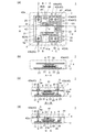
- FIG. 1 (a) is a top view of the inside of the semiconductor device 1
- FIG. 1 (b) is a sectional view taken along the line AA
- FIG. 1 (c) is a sectional view taken along the line BB
- FIG. 1D is a sectional view taken along line CC.
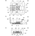
- FIG. 3A is a top view
- FIG. 3B is a cross-sectional view taken along the line DD.
- FIG. 4A is a top view of the inside of the semiconductor device 401
- FIG. 4B is a sectional view taken along line EE
- FIG. 4C is a sectional view taken along line FF.
- FIG. 4A is a top view of the inside of the semiconductor device 401
- FIG. 4B is a sectional view taken along line EE
- FIG. 4C is a sectional view taken along line FF.
- the semiconductor device 1 includes a built-in substrate 2, a semiconductor chip 3, a lead frame 4, and a pin terminal. 5 and a conductive joining member 6 are provided, and the lead frame 4 is resin-sealed with a mold resin 7 except for a part of the lead frame 4 and the tip end side of the pin terminal 5.
- the built-in board 2 is an electric circuit board.
- An appropriate substrate for example, a printed circuit board
- the internal substrate 2 of the embodiment is one surface of the insulating base material 21 and the insulating base material 21 for mounting the chip.
- the chip connection terminal 22 exposed to the surface, the plurality of electric path terminals 23 that are part of the electric circuit and are exposed on one surface of the insulating base material 21, and the insulating base material 21 that is not electrically connected to the electric circuit.
- It is a DCB (Direct C Cincinnatipper Bonding) substrate having an insulating terminal 24 exposed on one surface and a heat-dissipating metal plate 25 exposed on the other surface of the insulating base material 21.
- the heat radiating metal plate 25 is exposed from the mold resin 7.
- the semiconductor chip 3 is mounted on the built-in substrate 2.
- the semiconductor chip 3 has a collector electrode 31 formed on one surface (the surface on the internal substrate 2 side) and an emitter electrode 32 formed on the other surface (the surface opposite to the surface on the internal substrate 2 side).
- an IGBT having a gate electrode 33 formed at a position separated from the emitter electrode 32.
- the collector electrode 31 is bonded to the chip connection terminal 22 of the built-in substrate 2 via the conductive bonding member 6.
- the emitter electrode 32 is bonded to the lead frame 4 via the conductive bonding member 6.
- the gate electrode 33 is connected to the built-in substrate 2 via a conductive member such as a wire or a jumper.
- the lead frame 4 is made of a plurality of pieces of flat metal members, and is formed by being separated from the lead frame material 40 (see FIG. 2) described in 1.
- the lead frame 4 includes a lead frame collector piece 4C that is electrically connected to the collector electrode 31 of the semiconductor chip 3, a lead frame emitter piece 4E that is electrically connected to the emitter electrode 32 of the semiconductor chip 3, and a gate electrode 33 of the semiconductor chip 3. It is divided into a lead frame gate piece 4G that is electrically connected to the semiconductor chip and a lead frame insulation piece 4I that is not electrically connected to the semiconductor chip.
- the lead frame 4 has a larger cross-sectional area than the wire and can pass a large current.
- the lead frame 4 has a chip connection electrode portion 41, a substrate connection electrode portion 42, a horizontal plane support mechanism 43, and an insulating terminal connecting portion 44.
- the chip connection electrode portion 41, the substrate connection electrode portion 42, and the horizontal plane support mechanism 43 extend along the same plane, and the plane height is constant.
- the lead frame 4 is entirely covered with the mold resin 7 except for one end of the insulating terminal connecting portion 44.
- the chip connection electrode portion 41 is electrically connected to the emitter electrode 32 on the surface of the semiconductor chip 3 via the conductive bonding member 6.
- the chip connection electrode portion 41 is formed on the lead frame emitter piece 4E.
- the chip connection electrode portion 41 has an embossed protrusion 41a having a height corresponding to the thickness of the conductive bonding member 6 with the semiconductor chip 3 at the center of the surface on the semiconductor chip 3 side.
- the chip connection electrode portion 41 has a certain amount of gap secured between the surface thereof and the surface of the semiconductor chip 3, and is bonded to the semiconductor chip 3 via a conductive bonding member 6 having a sufficient thickness. ..
- the board connection electrode portion 42 is electrically connected to the electric path terminal 23 of the built-in board 2 via a pin terminal 5 described later.
- the substrate connection electrode portion 42 is formed with a through hole 42a corresponding to the external shape of the pin terminal 5, which will be described later, at a position where it overlaps with the electric path terminal 23 of the internal substrate 2 when it is overlapped with the internal substrate 2. See also FIG. 2).
- the substrate connection electrode portion 42 is formed on each of the lead frame collector piece 4C, the lead frame emitter piece 4E, and the lead frame gate piece 4G. A part of the substrate connection electrode portion 42 in the lead frame emitter piece 4E is connected to the chip connection electrode portion 41.
- Each of the horizontal plane support mechanisms 43 is composed of a plurality of horizontal plane support portions that project outward from the chip connection electrode portion 41 or the substrate connection electrode portion 42 when viewed in a plane.
- the horizontal plane support mechanism 43 is composed of a first horizontal plane support portion 43a and a plurality of second horizontal plane support portions 43b, each of which serves as a horizontal plane support portion.
- the first horizontal plane support portion 43a and the second horizontal plane support portion 43b are each formed to have the same width. Further, the tips of the first horizontal surface support portion 43a and the second horizontal plane support portion 43b are not in contact with the built-in substrate 2 and the semiconductor chip 3, and are not connected to any of them.
- the first horizontal surface support portion 43a projects from the opposite side of one set of the built-in substrate 2 (the side facing in the lateral direction in FIG. 1A).
- the first horizontal surface support portion 43a is formed on each of the lead frame collector piece 4C, the lead frame emitter piece 4E, and the lead frame gate piece 4G.
- the first horizontal surface support portion 43a of the lead frame emitter piece 4E projects from the chip connection electrode portion 41.
- the second horizontal surface support portion 43b projects from the opposite side of the other set of the built-in substrate 2 (the side facing in the vertical direction in FIG. 1A).
- the second horizontal surface support portion 43b is formed on each of the lead frame collector piece 4C, the lead frame emitter piece 4E, and the lead frame gate piece 4G.
- the second horizontal surface support portion 43b of the lead frame emitter piece 4E projects from the substrate connection electrode portion 42.
- the insulating terminal connecting portion 44 is electrically connected to the insulating terminal 24 of the built-in substrate 2 via the conductive joining member 6.
- the insulating terminal connecting portion 44 is bent in a crank shape, one end thereof is connected to the insulating terminal 24, and the other end is slightly exposed from the side surface of the mold resin 7.
- the insulating terminal connecting portion 44 is formed on the lead frame insulating piece 4I.
- the pin terminal 5 is an elongated columnar conductive pin having a flange portion 5a having a large diameter portion in the center portion.
- the pin terminal 5 is inserted into the through hole 42a of the lead frame 4 from one side opposite to the built-in substrate 2 side, and is arranged so as to stand perpendicular to the plane of the substrate connection electrode portion 42.
- One end of the pin terminal 5 is joined to the built-in substrate 2 via the conductive joining member 6, and one surface of the flange portion 5a is joined to the lead frame 4 via the conductive joining member 6. ..
- the pin terminal 5 is electrically connected to the substrate connection electrode portion 42 of the lead frame 4, and is also electrically connected to the electric path terminal 23 on the built-in substrate 2.
- the other side of the pin terminal 5 projects from the surface of the mold resin 7 and functions as an external connection terminal.
- the conductive joining member 6 is an alloy or metal having conductivity and adhesiveness.
- a silver paste, a conductive adhesive having silver nanoparticles, or the like may be adopted, but in the conductive bonding member 6 of the present embodiment, the solder material is heated and melted to be solidified. It is solder.
- the conductive joining member 6 may be lead-free solder.
- the conductive bonding member 6 is used at a plurality of locations between each terminal of the built-in substrate 2, each electrode of the semiconductor chip 3, the lead frame 4, or the pin terminal 5, and mechanically joins and electrically connects the two. To do.
- the mold resin 7 is a part of the heat-dissipating metal plate 25 of the built-in substrate 2, a part of the insulating terminal connecting portion 44 of the lead frame 4, and a part of the pin terminal 5. Except for, the built-in substrate 2, the semiconductor chip 3, the lead frame 4, the pin terminal 5, and the conductive bonding member 6 are resin-sealed.
- the lead frame 4 is composed of a plurality of pieces, but is formed by being separated from the lead frame material 40 of 1 in the manufacturing process.
- the lead frame material 40 used for manufacturing the semiconductor device 1 of the present embodiment will be described.
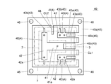
- the lead frame material 40 is a lead frame material processed into the lead frame 4 in the semiconductor device 1, and as shown in FIG. 2, the outer frame portion 45, the chip connection electrode portion 41, and the substrate connection electrode portion 42 It has a first horizontal surface support portion 43a, a second horizontal plane support portion 43b, and an insulated terminal connecting portion 44.
- the outer frame portion 45, the chip connection electrode portion 41, the substrate connection electrode portion 42, the first horizontal plane support portion 43a and the second horizontal plane support portion 43b are spread along the same plane as a whole. Is a rectangular metal flat plate having an opening and a through hole inside.
- the lead frame material 40 is separated along the first cut line CL1 and the second cut line CL2 so that the inside is separated as the lead frame 4. Since the parts of the lead frame material 40 other than the outer frame portion 45 are basically the same as the above-described lead frame 4, the detailed form will be omitted below.
- the outer frame portion 45 of the lead frame material 40 has a frame portion 45a and a connecting portion 45b, and surrounds the periphery of the built-in substrate 2 when superposed on the built-in substrate 2 and viewed in a plane.
- the frame portion 45a is formed in a rectangular frame shape.
- Positioning through holes 46 may be formed in the frame portion 45a at four corners or the like.
- the connecting portion 45b connects the frame portion 45a and the portion serving as the inner lead frame 4.
- the connecting portion 45b connects the frame portion 45a and the first horizontal plane supporting portion 43a.
- the positioning through holes 46 are drawn in a perfect circle at four locations, but may be partially formed into an elliptical shape or formed at only two locations in consideration of relief. May be good.
- the chip connection electrode portion 41 in the lead frame material 40 is a portion that becomes the chip connection electrode portion 41 in the lead frame 4, and when the lead frame material 40 is superposed on the built-in substrate 2 and viewed in a plane, at least a part thereof is connected to the semiconductor chip 3. Overlap. Also in the chip connection electrode portion 41 of the lead frame material 40, a protrusion 41a is formed in the center.
- the substrate connection electrode portion 42 in the lead frame material 40 is a portion that becomes the substrate connection electrode portion 42 in the lead frame 4, and at least a part of the internal substrate 2 is viewed in a plan view by being superposed on the internal substrate 2. It overlaps with the electric path terminal 23. Also in the substrate connection electrode portion 42 of the lead frame material 40, a through hole 42a is formed at a position overlapping the electric path terminal 23 when superposed on the built-in substrate 2 and viewed in a plane.
- the first horizontal plane support portion 43a in the lead frame material 40 is a portion serving as the first horizontal plane support portion 43a in the lead frame 4, and one end thereof is connected to the chip connection electrode portion 41 or the substrate connection electrode portion 42. Further, the first horizontal surface support portion 43a of the lead frame material 40 is not connected to anything when the other end is separated as the lead frame 4, but before being separated, it is connected to the connecting portion 45b of the outer frame portion 45. It is connected.
- the second horizontal plane support portion 43b in the lead frame material 40 is a portion that becomes the second horizontal plane support portion 43b in the lead frame 4, one end is connected to the substrate connection electrode portion 42, and the other end is outside the built-in substrate 2. It is located and not connected to anything.
- the insulated terminal connecting portion 44 in the lead frame material 40 is a portion that becomes the insulated terminal connecting portion 44 in the lead frame 4, and one end of the lead frame material 40 overlaps the insulated terminal 24 when it is overlapped with the built-in substrate 2 and viewed in a plane. Further, the insulated terminal connecting portion 44 of the lead frame material 40 is not connected to anything when the other end is separated as the lead frame 4, but is connected to the frame portion 45a of the outer frame portion 45 before being disconnected. There is.
- a fixing jig 80 having a recess inside as shown in FIG. 3 is used to mount the component.
- the concave portion of the fixing jig 80 has a bottom surface 81 having an outer shape corresponding to the outer shape of the built-in substrate 2 at a depth dimension position corresponding to the distance dimension between one surface of the lead frame 4 and one surface of the semiconductor chip 3.
- the fixing jig 80 has a lead frame material mounting surface 82 on the upper surface, and a positioning pin 83 projects from a part of the lead frame material mounting surface 82 in accordance with the positioning through hole 46 of the lead frame material 40.
- the bottom surface 81 and the lead frame material mounting surface 82 are flat surfaces parallel to each other.
- the fixing jig 80 When mounting components in the manufacturing process of the semiconductor device 1, as shown in FIG. 3B, the fixing jig 80 has a built-in substrate 2, a semiconductor chip 3, a lead frame material 40 having a lead frame 4 inside, and a pin terminal 5. After the conductive joining member 6 in the unsolidified state is arranged, the conductive joining member 6 is solidified.
- the built-in board 2 with the chip connection terminal 22 facing upward is placed on the bottom surface 81 of the fixing jig 80.
- the conductive bonding member 6 (solder material) is applied to the chip connection terminal 22 and the electric path terminal 23 of the built-in substrate 2.
- the semiconductor chip 3 with the collector electrode 31 facing downward is placed on the chip connection terminal 22 of the built-in substrate 2.
- the conductive bonding member 6 (solder material) is applied to the emitter electrode 32 of the semiconductor chip 3.
- the lead frame material 40 is placed on the lead frame material mounting surface 82 of the fixing jig 80.
- the conductive bonding member 6 (solder material) is applied to the substrate connection electrode portion 42 of the lead frame material 40.
- the pin terminal 5 is inserted into the through hole 42a of the substrate connection electrode portion 42 of the lead frame material 40 so that the lower end is in contact with the conductive joining member 6 on the electric path terminal 23 of the built-in substrate 2.
- the built-in substrate 2, the semiconductor chip 3, the lead frame 4, the pin terminal 5, and the conductive joining member 6 are arranged on the fixing jig 80 as shown in FIG.
- the built-in substrate 2, the semiconductor chip 3, the lead frame material 40 having the lead frame 4 inside, and the pin terminal 5 are integrated by the conductive bonding member 6.
- solder material a paste-like solder material (so-called cream solder), a solid-state solder material (so-called plate solder), or a combination thereof can be used.
- the lead frame 4 having the horizontal plane support portions 43a and 43b protruding from the chip connection electrode portion 41 or the substrate connection electrode portion 42 to the outside of the built-in substrate 2 when viewed in a plan view is provided. Therefore, since the lead frame 4 can be arranged while suppressing the inclination by receiving the horizontal plane support portions 43a and 43b with the fixing jig 80 at the time of manufacturing, the tip pitch accuracy of the external connection terminal to be joined to the lead frame 4 can be improved. Further, according to the semiconductor device 1, since the pin terminal 5 standing in the direction perpendicular to the plane of the substrate connection electrode portion 42 is provided, a pin terminal structure in which the external connection terminal is the pin terminal 5 can be configured. As a result, the semiconductor device 1 becomes a semiconductor device having a pin terminal structure with good tip pitch accuracy of the external connection terminal.
- the tips of the horizontal support portions 43a and 43b are not in contact with the built-in substrate 2 and the semiconductor chip 3 and are not connected to any of them. Therefore, when the tips of the horizontal support portions 43a and 43b are manufactured. It can be used for leveling the lead frame 4 in.
- the chip connection electrode portion 41, the substrate connection electrode portion 42, and the horizontal plane support portions 43a and 43b of the lead frame 4 are spread along the same plane, they are bent or the like between the respective portions. Therefore, it is easy to improve the flatness accuracy of each part of the lead frame 4.
- the pin terminal 5 is electrically connected to the electric path terminal 23 on the built-in substrate 2 via the conductive joining member 6. Therefore, according to the semiconductor device 1, the tip pitch accuracy of the pin terminal 5 as the external connection terminal can be easily obtained.
- the lead frame 4 has a horizontal plane support mechanism 43 composed of a plurality of first horizontal plane support portions 43a and a plurality of second horizontal plane support portions 43b.
- the first horizontal plane support portion 43a projects from the opposite side of one set of the built-in substrate 2
- the second horizontal plane support portion 43b projects from the opposite side of the other set of the built-in substrate 2. Therefore, according to the semiconductor device 1, since the lead frame 4 can be supported by a line other than the line along one side at the time of manufacturing, the lead frame 4 can be configured with the inclination suppressed.
- the plurality of horizontal plane support portions 43a and 43b constituting the horizontal plane support mechanism 43 of the lead frame 4 are formed to have the same width. Therefore, according to the semiconductor device 1, when the conductive bonding member 6 is solidified at the time of manufacturing, the bias of the thermal stress in the chip connection electrode portion 41 and the substrate connection electrode portion 42 of the lead frame 4 is suppressed, so that the inclination is suppressed.
- the lead frame 4 can be configured by suppressing the above.
- the chip connection electrode portion 41 of the lead frame 4 has a protrusion 41a having a height corresponding to the thickness of the conductive bonding member 6 on the surface of the semiconductor chip 3. Therefore, according to the semiconductor device 1, when the conductive bonding member 6 is solidified during manufacturing, even if the semiconductor chip 3 floats, it can be suppressed by the embossed protrusion 41a. Therefore, the semiconductor chip 3 and the lead frame A conductive joint member 6 having a sufficient thickness necessary for maintaining performance can be formed between the conductor and the member 4.
- the lead frame 4 has an insulating terminal connecting portion 44 electrically connected to the insulating terminal 24 of the built-in substrate 2 via a conductive joining member 6, and the insulating terminal connecting portion 44 All but a part is covered with the mold resin 7. Therefore, according to the semiconductor device 1, since the terminal connected to the electric circuit of the built-in substrate 2 is not exposed on the side surface, it can be configured to be excellent in high withstand voltage.
- the lead frame material 40 one end is connected to the chip connection electrode portion 41 or the substrate connection electrode portion 42, and the other end is connected to the outer frame portion 45 when the lead frame material 40 is superposed on the built-in substrate 2 and viewed in a plane. It includes a horizontal plane support portion 43a, one end of which is connected to the substrate connection electrode portion 42, the other end of which is located outside the built-in substrate 2, and a second horizontal plane support portion 43b which is not connected to anything. Therefore, according to the lead frame material 40, the lead frame material 40 can be arranged while suppressing the inclination by receiving the first and second horizontal surface support portions 43a and 43b with the fixing jig 80 at the time of manufacturing. The tip pitch accuracy of the external connection terminal to be joined can be improved.
- the lead frame material 40 includes a substrate connection electrode portion 42 in which at least a part thereof overlaps with the electric path terminal 23 of the built-in substrate 2 when superposed on the built-in substrate 2 and viewed in a plane. Therefore, according to the lead frame material 40, since the pin terminal 5 can be joined to the electric path terminal 23 of the built-in board 2 via the substrate connection electrode portion 42, the pin terminal structure in which the external connection terminal is the pin terminal 5 Can be configured. As a result, the lead frame material 40 becomes a lead frame material used in the semiconductor device 1 having a pin terminal structure having a good tip pitch accuracy of the external connection terminal.
- the outer frame portion 45, the chip connection electrode portion 41, the substrate connection electrode portion 42, and the first and second horizontal plane support portions 43a and 43b extend along the same plane. Therefore, the flatness accuracy of each part of the lead frame 4 formed by separating the inside can be improved.
- the tip of the lead frame material 40 is used as the electric path terminal 23.
- the pin terminal 5 to be joined can be erected.
- the lead frame material 40 when the lead frame material 40 is superposed on the built-in substrate 2 on which the insulating terminal 24 is formed and viewed in a plane, one end overlaps the insulating terminal 24 and the other end is connected to the outer frame portion 45. It further has a connecting portion 44. Therefore, according to the lead frame material 40, since the internal parts of the semiconductor device 1 can be supported by the outer frame portion 45 connected to the insulating terminal connecting portion 44 which is not connected to the electric circuit at the time of manufacturing, the resin made of the mold resin 7 is used. The workability of sealing can be improved.
- the semiconductor chip 3 is an IGBT, but the present invention is not limited thereto.
- the semiconductor chip 3 may be another three-terminal semiconductor element (for example, MOSFET), the semiconductor chip 3 may be a two-terminal semiconductor element (for example, a diode), and the semiconductor chip 3 may be a semiconductor element with four or more terminals (4).
- the semiconductor element of the terminal may be, for example, a thyristor).
- the semiconductor device is a semiconductor device including one semiconductor chip, but the present invention is not limited thereto.
- the semiconductor device may be a semiconductor device including two semiconductor chips, or a semiconductor device including three or more semiconductor chips.
- the semiconductor device is a so-called vertical semiconductor device having a collector electrode on one surface of the semiconductor chip and an emitter electrode and a gate electrode on the other surface. It is not limited to this.
- the semiconductor device may be a so-called horizontal semiconductor device having all electrodes on the surface opposite to the substrate side.
- the chip connection electrode portion 41, the substrate connection electrode portion 42, and the first and second horizontal plane support portions 43a and 43b extend along the same plane.
- the present invention is not limited to this.
- the chip connection electrode portion of the lead frame, the substrate connection electrode portion, and the first and second horizontal plane support portions are preferably spread along the same plane, but may be partially displaced in parallel.
- the tip of the first horizontal support portion 43a is connected to the outer frame portion 45 and the tip of the second horizontal support portion 43b is not connected to any part.
- the present invention is not limited to this.
- the tip of the first horizontal support portion may not be connected to any part, and the tip of the second horizontal support portion may be connected to the outer frame portion.
- the lead frame material may be one in which the tips of the first and second horizontal surface support portions are both connected to the outer frame portion.
- the lead frame 4 has been described as having the first and second horizontal surface support portions 43a and 43b, but the present invention is not limited thereto.
- the lead frame may have either a first or second horizontal plane support.
- the pin terminal 5 of the above embodiment has been described as having a columnar shape, the present invention may be limited to this.
- the pin terminal may be a prismatic one or a thin plate-shaped one.
Landscapes
- Lead Frames For Integrated Circuits (AREA)
Abstract
半導体装置1は、半導体チップ3が実装され、表面に電気経路端子23を含む端子が形成された内蔵基板2と、半導体チップ3の表面に導電性接合部材6を介して電気的に接続されたチップ接続電極部41、内蔵基板2の電気経路端子23に電気的に接続された基板接続電極部42、チップ接続電極部41若しくは基板接続電極部42から外側に張り出す水平面支持部43を有するリードフレーム4と、リードフレーム4の基板接続電極部42の平面に対して垂直方向に立つピン端子5とを備え、水平面支持部43は、内蔵基板2より外側まで張り出していることを特徴とする。 本発明によれば、外部接続端子の先端ピッチ精度が良好なピン端子構造の半導体装置を提供することができる。
Description
本発明は、半導体装置、及びリードフレーム材に関する。
特許文献1には、内蔵基板上や、内蔵基板上に実装されている半導体チップ上に、導電性接合部材を介してリードフレームが接合された半導体装置が開示されている。このような半導体装置のリードフレームは、製造時に、リードフレーム材として外枠部内側に繋がった状態で半導体チップ上及び内蔵基板上に接合され、その後外枠部から切り離される。また、特許文献2には、外部接続端子がピン端子構造の半導体装置が開示されている。
特許文献1に開示された従来の半導体装置601は、図4(a)に示すように、半導体チップ403が実装された内蔵基板402と、内蔵基板402及び半導体チップ403上に導電性接合部材406を介して接合されたリードフレーム404と、これらを一部残して樹脂封止しているモールド樹脂407とを備えている。製造時リードフレーム材の状態において、リードフレーム404が外枠部(不図示)と接合している部分445は、図4(a)及び図4(b)に示すように、外部接続端子としてモールド樹脂407から露出している。
また、半導体装置401において、リードフレーム404は、半導体チップ403の電極に接合するチップ接続電極部441と、チップ接続電極部441から半導体チップ403の外形外側まで張り出させた部分443とを有している。張り出させた部分443の先端は、図4(c)に示すように、内蔵基板402上の電気経路端子423の一部に導電性接合部材406を介して接合されている。リードフレーム404は、張り出させた部分443が薄い導電性接合部材406を介して内蔵基板402で受けられているため、製造時、自重による傾きがある程度抑えられた状態で接合される。
特許文献2に開示された従来の半導体装置501は、いわゆるピン端子構造の半導体装置であり、図5に示すように、外部接続端子として、内蔵基板502上に接合されたピン端子505を備えている。ピン端子505は、内蔵基板502表面に対して垂直に立てられ、モールド樹脂507から露出している。このようなピン端子構造の半導体装置は、電気経路を短くできる。
しかしながら、上記した半導体装置401では、張り出させた部分443が、薄いと言っても導電性接合部材406を介して受けられているため、リードフレーム404が自重で傾いて接合されてしまう虞がある。また、半導体装置401では、張り出させた部分443が内蔵基板402によって受けられているため、内蔵基板402が傾いていた場合、リードフレーム404がモールド樹脂407に対して傾いて接合されてしまう虞がある。リードフレームが傾いて接合されてしまうと、外部接続端子の先端ピッチ精度が悪化してしまうという問題がある。特に、ピン端子構造の半導体装置の場合には、ピン端子を立てる表面に傾きがあるとピン端子が傾き、ピン端子の先端ピッチ精度が悪化してしまうという問題がある。
そこで、本発明は、上記した問題を解決するためになされたもので、外部接続端子の先端ピッチ精度が良好なピン端子構造の半導体装置を提供することを目的とする。また、本発明は、外部接続端子の先端ピッチ精度が良好なピン端子構造の半導体装置に用いられるリードフレーム材を提供することを目的とする。
[1]本発明の半導体装置は、半導体チップが実装され、表面に電気経路端子を含む端子が形成された内蔵基板と、前記半導体チップの表面に導電性接合部材を介して電気的に接続されたチップ接続電極部、前記内蔵基板の電気経路端子に電気的に接続された基板接続電極部、及び平面的に見て前記チップ接続電極部若しくは前記基板接続電極部から外側に張り出す水平面支持部を有するリードフレームと、前記リードフレームの前記基板接続電極部に電気的に接続されているとともに前記基板接続電極部の平面に対して垂直方向に立つピン端子とを備え、前記水平面支持部は、平面的に見て前記内蔵基板より外側まで張り出していることを特徴とする。
[2]本発明の半導体装置においては、前記水平面支持部の先端は、前記内蔵基板及び前記半導体チップに接していないことが好ましい。
[3]本発明の半導体装置においては、前記チップ接続電極部、前記基板接続電極部、及び前記水平面支持部は、同一平面に沿って広がっており、前記ピン端子は、前記内蔵基板上の前記電気経路端子に導電性接合部材を介して電気的に接続されていることが好ましい。
[4]本発明の半導体装置においては、前記リードフレームは、前記水平面支持部として、前記内蔵基板の一方組の対辺から張り出している第1の水平面支持部と前記内蔵基板の他方組の対辺から張り出している第2の水平面支持部とを有し、前記第1の水平面支持部及び前記第2の水平面支持部によって、水平面支持機構が構成されていることが好ましい。
[5]本発明の半導体装置においては、前記水平面支持機構を構成する複数の前記水平面支持部は、同等幅で形成されていることが好ましい。
[6]本発明の半導体装置においては、前記チップ接続電極部は、前記半導体チップの表面の導電性接合部材の厚みに対応する高さの打ち出し突起を有することが好ましい。
[7]本発明の半導体装置においては、前記内蔵基板は、絶縁端子をさらに有し、前記リードフレームは、前記絶縁端子に導電性接合部材を介して電気的に接続された絶縁端子連結部をさらに有し、当該絶縁端子連結部の一部以外が全てモールド樹脂に覆われていることが好ましい。
[8]本発明のリードフレーム材は、半導体チップが実装され、表面に電気経路端子を含む端子が形成された内蔵基板と、前記半導体チップ及び前記内蔵基板に電気的に接続されたリードフレームとを備える半導体装置における前記リードフレームに加工されるリードフレーム材であって、前記内蔵基板に重ね合わせて平面的に見た際に、前記内蔵基板を囲う枠状の外枠部と、少なくとも一部が前記半導体チップと重なるチップ接続電極部と、少なくとも一部が前記内蔵基板の前記電気経路端子と重なる基板接続電極部と、一端が前記チップ接続電極部又は前記基板接続電極部に繋がり、他端が前記外枠部に繋がる第1の水平面支持部と、一端が前記基板接続電極部と繋がり、他端が前記内蔵基板の外側に位置するとともに、どことも繋がらない第2の水平面支持部と、を有することを特徴とする。
[9]本発明のリードフレーム材においては、前記外枠部、前記チップ接続電極部、前記基板接続電極部、及び前記水平面支持部は、同一平面に沿って広がっていることが好ましい。
[10]本発明のリードフレーム材においては、前記内蔵基板に重ね合わせて平面的に見た際に、前記電気経路端子と重なる位置に貫通孔が形成されていることが好ましい。
[11]本発明のリードフレーム材においては、前記端子の一部として絶縁端子が形成された前記内蔵基板に重ね合わせて平面的に見た際に、一端が前記絶縁端子に重なり、他端が前記外枠部に繋がる絶縁端子連結部をさらに有することが好ましい。
本発明の半導体装置によれば、平面的に見てチップ接続電極部若しくは基板接続電極部から内蔵基板よりも外側まで張り出す水平面支持部を有するリードフレームを備えるため、製造時に固定冶具で水平面支持部を受けることで傾きを抑えてリードフレームを配置できることから、リードフレームと接合する外部接続端子の先端ピッチ精度を良好にできる。また、本発明の半導体装置によれば、基板接続電極部の平面に対して垂直方向に立つピン端子を備えるため、外部接続端子をピン端子とするピン端子構造を構成できる。その結果、本発明の半導体装置は、外部接続端子の先端ピッチ精度が良好なピン端子構造の半導体装置となる。
本発明のリードフレーム材においては、内蔵基板に重ね合わせて平面的に見た際に、一端がチップ接続電極部又は基板接続電極部に繋がり、他端が外枠部に繋がる第1の水平面支持部と、一端が基板接続電極部と繋がり、他端が内蔵基板の外側に位置するとともに、どことも繋がらない第2の水平面支持部とを備える。このため、本発明のリードフレーム材によれば、製造時に固定冶具で第1及び第2の水平面支持部を受けることで傾きを抑えてリードフレーム材を配置できることから、リードフレーム材と接合する外部接続端子の先端ピッチ精度を良好にできる。また、本発明のリードフレーム材は、内蔵基板に重ね合わせて平面的に見た際に、少なくとも一部が内蔵基板の電気経路端子と重なる基板接続電極部を備えるため、基板接続電極部を介してピン端子を内蔵基板の電気経路端子に接合可能なことから、外部接続端子をピン端子とするピン端子構造を構成できる。その結果、本発明のリードフレーム材は、外部接続端子の先端ピッチ精度が良好なピン端子構造の半導体装置に用いられるリードフレーム材となる。
以下、本発明の半導体装置について、図に示す実施形態に基づいて説明する。なお、各図面は模式図であり、必ずしも実際の寸法を厳密に反映したものではない。
1.実施形態における半導体装置1の構成
実施形態に係る半導体装置1は、図1(a)~(d)に示すように、内蔵基板2と、半導体チップ3と、リードフレーム4と、ピン端子5と、導電性接合部材6と、を備え、リードフレーム4の一部及びピン端子5の先端側を除いてモールド樹脂7で樹脂封止されている。
実施形態に係る半導体装置1は、図1(a)~(d)に示すように、内蔵基板2と、半導体チップ3と、リードフレーム4と、ピン端子5と、導電性接合部材6と、を備え、リードフレーム4の一部及びピン端子5の先端側を除いてモールド樹脂7で樹脂封止されている。
内蔵基板2は、電気回路基板である。内蔵基板としては適宜の基板(例えば、プリント基板)を用いることができるが、実施形態の内蔵基板2は、絶縁性基材21と、チップを搭載するために絶縁性基材21の一方の表面に露出するチップ接続端子22と、電気回路の一部であり絶縁性基材21の一方の表面に露出する複数の電気経路端子23と、電気回路と電気的に繋がらず絶縁性基材21の一方の表面に露出する絶縁端子24と、絶縁性基材21の他方の面に露出する放熱用金属板25とを有するDCB(Direct Cоpper Bonding)基板である。なお、放熱用金属板25はモールド樹脂7から露出している。
半導体チップ3は、内蔵基板2上に実装されている。半導体チップ3は、一方の面(内蔵基板2側の面)に形成されたコレクタ電極31、並びに、他方の面(内蔵基板2側の面とは反対側の面)に形成されたエミッタ電極32、及びエミッタ電極32とは離間した位置に形成されたゲート電極33を有するIGBTである。コレクタ電極31は、導電性接合部材6を介して内蔵基板2のチップ接続端子22に接合されている。エミッタ電極32は、導電性接合部材6を介してリードフレーム4に接合されている。ゲート電極33は、ワイヤやジャンパー等の導電性部材を介して内蔵基板2に接続されている。
リードフレーム4は、複数ピースの平板状の金属部材からなり、後述の1のリードフレーム材40(図2参照)から切り離されて形成されたものである。リードフレーム4は、半導体チップ3のコレクタ電極31と電気的に接続するリードフレームコレクタピース4C、半導体チップ3のエミッタ電極32と電気的に接続するリードフレームエミッタピース4E、半導体チップ3のゲート電極33と電気的に接続するリードフレームゲートピース4G、及び半導体チップと電気的に接続していないリードフレーム絶縁ピース4Iに分割されている。リードフレーム4は、ワイヤよりも断面積が大きく、大電流を流すことができる。リードフレーム4は、チップ接続電極部41と、基板接続電極部42と、水平面支持機構43と、絶縁端子連結部44とを有している。チップ接続電極部41、基板接続電極部42、及び水平面支持機構43は、同一平面に沿って広がっており、平面高さは一定である。リードフレーム4は、絶縁端子連結部44の一端部以外が全てモールド樹脂7に覆われている。
チップ接続電極部41は、導電性接合部材6を介して半導体チップ3の表面のエミッタ電極32に電気的に接続されている。チップ接続電極部41は、リードフレームエミッタピース4Eに形成されている。チップ接続電極部41は、半導体チップ3側の表面中央部に、半導体チップ3との間の導電性接合部材6の厚みに対応する高さの打ち出し突起41aを有する。チップ接続電極部41は、半導体チップ3上に載置された際、打ち出し突起41aの頂点が半導体チップ3に接触する。このため、チップ接続電極部41は、その表面と半導体チップ3の表面との間に一定量の隙間が確保され、十分な厚みの導電性接合部材6を介して半導体チップ3に接合されている。
基板接続電極部42は、後述のピン端子5を介して内蔵基板2の電気経路端子23に電気的に接続されている。基板接続電極部42には、内蔵基板2と重ね合わせた際に内蔵基板2の電気経路端子23と重なる位置に、後述のピン端子5の外形形状に対応した貫通孔42aが形成されている(図2も併せて参照)。基板接続電極部42は、リードフレームコレクタピース4C、リードフレームエミッタピース4E、及びリードフレームゲートピース4Gのそれぞれに形成されている。なお、リードフレームエミッタピース4Eにおける基板接続電極部42は、一部がチップ接続電極部41と繋がっている。
水平面支持機構43は、それぞれが、平面的に見てチップ接続電極部41若しくは基板接続電極部42から外側に張り出す複数の水平面支持部によって構成されている。水平面支持機構43は、それぞれが水平面支持部となる第1の水平面支持部43a及び複数の第2の水平面支持部43bによって構成されている。第1の水平面支持部43a及び第2の水平面支持部43bは、それぞれ同等の幅で形成されている。また、第1の水平面支持部43a及び第2の水平面支持部43bの先端は、内蔵基板2及び半導体チップ3に接しておらず、どことも繋がっていない。
第1の水平面支持部43aは、内蔵基板2の一方組の対辺(図1(a)において横方向に対向する辺)から張り出している。第1の水平面支持部43aは、リードフレームコレクタピース4C、リードフレームエミッタピース4E、及びリードフレームゲートピース4Gのそれぞれに形成されている。なお、リードフレームエミッタピース4Eにおける第1の水平面支持部43aは、チップ接続電極部41から張り出している。
第2の水平面支持部43bは、内蔵基板2の他方組の対辺(図1(a)において縦方向に対向する辺)から張り出している。第2の水平面支持部43bは、リードフレームコレクタピース4C、リードフレームエミッタピース4E、及びリードフレームゲートピース4Gのそれぞれに形成されている。なお、リードフレームエミッタピース4Eにおける第2の水平面支持部43bは、基板接続電極部42から張り出している。
絶縁端子連結部44は、導電性接合部材6を介して内蔵基板2の絶縁端子24に電気的に接続されている。絶縁端子連結部44は、クランク状に曲げられて、一端が絶縁端子24に接続され、他端がモールド樹脂7の側面から僅かに露出している。絶縁端子連結部44は、リードフレーム絶縁ピース4Iに形成されている。
ピン端子5は、中央部に径が大きな部分のフランジ部5aを有する細長い円柱状の導電性ピンである。ピン端子5は、リードフレーム4の貫通孔42aに内蔵基板2側と反対側から一方側を差し込まれ、基板接続電極部42の平面に対して垂直方向に立つよう配置される。ピン端子5は、一方側の端部が導電性接合部材6を介して内蔵基板2に接合され、フランジ部5aの一方側の面が導電性接合部材6を介してリードフレーム4に接合される。これにより、ピン端子5は、リードフレーム4の基板接続電極部42に電気的に接続されるとともに、内蔵基板2上の電気経路端子23に電気的に接続される。ピン端子5は、他方側がモールド樹脂7の表面から突出し、外部接続端子として機能する。
導電性接合部材6は、導電性および接着性を有する合金又は金属である。導電性接合部材としては、銀ペーストや銀ナノ粒子を有する導電性接着剤等を採用してもよいが、本実施形態の導電性接合部材6は、はんだ材を加熱・溶融して固化させたはんだである。導電性接合部材6は、鉛フリーはんだでもよい。導電性接合部材6は、内蔵基板2の各端子、半導体チップ3の各電極、リードフレーム4、又はピン端子5の間で複数箇所に用いられ、両者を機械的に接合するとともに電気的に接続する。
モールド樹脂7には適宜の樹脂が用いられ、モールド樹脂7は、内蔵基板2の放熱用金属板25の一部、リードフレーム4の絶縁端子連結部44の一部、及びピン端子5の一部を除き、内蔵基板2、半導体チップ3、リードフレーム4、ピン端子5、及び導電性接合部材6を樹脂封止している。
2.実施形態におけるリードフレーム材40の構成
前述したように、リードフレーム4は、複数ピースからなるが、製造過程において1のリードフレーム材40から切り離されて形成されたものである。ここで、本実施形態の半導体装置1の製造に用いられるリードフレーム材40について説明する。リードフレーム材40は、半導体装置1におけるリードフレーム4に加工されるリードフレーム材であって、図2に示すように、外枠部45と、チップ接続電極部41と、基板接続電極部42と、第1の水平面支持部43aと、第2の水平面支持部43bと、絶縁端子連結部44とを有している。リードフレーム材40は、外枠部45、チップ接続電極部41、基板接続電極部42、第1の水平面支持部43a及び第2の水平面支持部43bが同一平面に沿って広がっており、全体的には内側に開口と貫通孔とを有する矩形状の金属製平板である。リードフレーム材40は、製造時において、第1カットラインCL1及び第2カットラインCL2に沿って切り離されることで、内側がリードフレーム4として分離する。なお、リードフレーム材40における外枠部45以外の部分については、前述のリードフレーム4として説明した形態と基本的には同様であるため、以下においては詳細な形態を省略して説明する。
前述したように、リードフレーム4は、複数ピースからなるが、製造過程において1のリードフレーム材40から切り離されて形成されたものである。ここで、本実施形態の半導体装置1の製造に用いられるリードフレーム材40について説明する。リードフレーム材40は、半導体装置1におけるリードフレーム4に加工されるリードフレーム材であって、図2に示すように、外枠部45と、チップ接続電極部41と、基板接続電極部42と、第1の水平面支持部43aと、第2の水平面支持部43bと、絶縁端子連結部44とを有している。リードフレーム材40は、外枠部45、チップ接続電極部41、基板接続電極部42、第1の水平面支持部43a及び第2の水平面支持部43bが同一平面に沿って広がっており、全体的には内側に開口と貫通孔とを有する矩形状の金属製平板である。リードフレーム材40は、製造時において、第1カットラインCL1及び第2カットラインCL2に沿って切り離されることで、内側がリードフレーム4として分離する。なお、リードフレーム材40における外枠部45以外の部分については、前述のリードフレーム4として説明した形態と基本的には同様であるため、以下においては詳細な形態を省略して説明する。
リードフレーム材40における外枠部45は、枠部分45aと連結部分45bとを有し、内蔵基板2に重ね合わせて平面的に見た際に、内蔵基板2の周囲を囲う。枠部分45aは、矩形枠状に形成されている。枠部分45aには、4つ角等に位置決め用貫通孔46が形成されていてもよい。連結部分45bは、枠部分45aと内側のリードフレーム4となる部分とを繋いでいる。例えば、連結部分45bは、枠部分45aと第1の水平面支持部43aとを繋いでいる。なお、図2において、位置決め用貫通孔46は、4箇所に真円状で描かれているが、逃がしを考慮して部分的に楕円形状に形成したり、2箇所だけに形成したりしてもよい。
リードフレーム材40におけるチップ接続電極部41は、リードフレーム4におけるチップ接続電極部41となる部分であり、内蔵基板2に重ね合わせて平面的に見た際に、少なくとも一部が半導体チップ3と重なる。リードフレーム材40におけるチップ接続電極部41においても、中央に打ち出し突起41aが形成されている。
リードフレーム材40における基板接続電極部42は、リードフレーム4における基板接続電極部42となる部分であり、内蔵基板2に重ね合わせて平面的に見た際に、少なくとも一部が内蔵基板2の電気経路端子23と重なる。リードフレーム材40における基板接続電極部42においても、内蔵基板2に重ね合わせて平面的に見た際に、電気経路端子23と重なる位置に貫通孔42aが形成されている。
リードフレーム材40における第1の水平面支持部43aは、リードフレーム4における第1の水平面支持部43aとなる部分であり、一端がチップ接続電極部41又は基板接続電極部42に繋がっている。また、リードフレーム材40における第1の水平面支持部43aは、他端がリードフレーム4として切り離された際にはどことも繋がっていないが、切り離される前には外枠部45の連結部分45bに繋がっている。
リードフレーム材40における第2の水平面支持部43bは、リードフレーム4における第2の水平面支持部43bとなる部分であり、一端が基板接続電極部42と繋がり、他端が内蔵基板2の外側に位置するとともに、どことも繋がっていない。
リードフレーム材40における絶縁端子連結部44は、リードフレーム4における絶縁端子連結部44となる部分であり、内蔵基板2に重ね合わせて平面的に見た際に、一端が絶縁端子24に重なる。また、リードフレーム材40における絶縁端子連結部44は、他端がリードフレーム4として切り離された際にはどことも繋がっていないが、切り離される前には外枠部45の枠部分45aに繋がっている。
3.実施形態に係る半導体装置1の製造過程における部品実装
半導体装置1の製造過程においては、図3に示すような内側に凹部を有する固定冶具80が用いられて部品実装される。固定冶具80の凹部は、リードフレーム4の一方の面と半導体チップ3の一方の面との距離寸法に対応した深さ寸法位置において、内蔵基板2の外形形状に対応した外形形状の底面81を有している。固定冶具80は、上面において、リードフレーム材載置面82を有し、リードフレーム材載置面82の一部からは、リードフレーム材40の位置決め用貫通孔46に合わせて位置決めピン83が突出している。底面81とリードフレーム材載置面82とは、互いに平行な平面となっている。
半導体装置1の製造過程においては、図3に示すような内側に凹部を有する固定冶具80が用いられて部品実装される。固定冶具80の凹部は、リードフレーム4の一方の面と半導体チップ3の一方の面との距離寸法に対応した深さ寸法位置において、内蔵基板2の外形形状に対応した外形形状の底面81を有している。固定冶具80は、上面において、リードフレーム材載置面82を有し、リードフレーム材載置面82の一部からは、リードフレーム材40の位置決め用貫通孔46に合わせて位置決めピン83が突出している。底面81とリードフレーム材載置面82とは、互いに平行な平面となっている。
半導体装置1の製造過程における部品実装の際、図3(b)に示すように、固定冶具80に、内蔵基板2、半導体チップ3、内側にリードフレーム4を有するリードフレーム材40、ピン端子5、及び未固化状態の導電性接合部材6が配置された後、導電性接合部材6が固化される。
具体的には、まず、チップ接続端子22を上方に向けた内蔵基板2が固定冶具80の底面81に載置される。次に、内蔵基板2のチップ接続端子22及び電気経路端子23に導電性接合部材6(はんだ材)が塗布される。次に、コレクタ電極31を下方に向けた半導体チップ3が内蔵基板2のチップ接続端子22上に載置される。次に、半導体チップ3のエミッタ電極32に導電性接合部材6(はんだ材)が塗布される。次に、固定冶具80のリードフレーム材載置面82にリードフレーム材40が載置される。次に、リードフレーム材40の基板接続電極部42に導電性接合部材6(はんだ材)が塗布される。次に、ピン端子5が、下端を内蔵基板2の電気経路端子23上の導電性接合部材6に接触させるようにして、リードフレーム材40の基板接続電極部42の貫通孔42aに挿通されて立てられる。そうすると、固定冶具80に内蔵基板2、半導体チップ3、リードフレーム4、ピン端子5、及び導電性接合部材6が図3に示すように配置される。次に、全体が加熱されることで導電性接合部材6により内蔵基板2、半導体チップ3、内側にリードフレーム4を有するリードフレーム材40、及びピン端子5は一体化する。
なお、半導体装置1の製造過程における部品実装の際、半導体チップ3のゲート電極33と内蔵基板2とは、両者を繋ぐためにワイヤが用いられるか導電性接合部材を介する金属板が用いられるかによって、適宜上記具体的な手順の中で電気的に接合される。また、はんだ材としては、ペースト状のはんだ材(いわゆるクリームはんだ)や固体状のはんだ材(いわゆる板はんだ)またはこれらを組み合わせて用いることができる。
4.実施形態に係る効果
半導体装置1によれば、平面的に見てチップ接続電極部41若しくは基板接続電極部42から内蔵基板2よりも外側まで張り出す水平面支持部43a,43bを有するリードフレーム4を備えるため、製造時に固定冶具80で水平面支持部43a,43bを受けることで傾きを抑えてリードフレーム4を配置できることから、リードフレーム4と接合する外部接続端子の先端ピッチ精度を良好にできる。また、半導体装置1によれば、基板接続電極部42の平面に対して垂直方向に立つピン端子5を備えるため、外部接続端子をピン端子5とするピン端子構造を構成できる。その結果、半導体装置1は、外部接続端子の先端ピッチ精度が良好なピン端子構造の半導体装置となる。
半導体装置1によれば、平面的に見てチップ接続電極部41若しくは基板接続電極部42から内蔵基板2よりも外側まで張り出す水平面支持部43a,43bを有するリードフレーム4を備えるため、製造時に固定冶具80で水平面支持部43a,43bを受けることで傾きを抑えてリードフレーム4を配置できることから、リードフレーム4と接合する外部接続端子の先端ピッチ精度を良好にできる。また、半導体装置1によれば、基板接続電極部42の平面に対して垂直方向に立つピン端子5を備えるため、外部接続端子をピン端子5とするピン端子構造を構成できる。その結果、半導体装置1は、外部接続端子の先端ピッチ精度が良好なピン端子構造の半導体装置となる。
また、半導体装置1によれば、水平面支持部43a,43bの先端は、内蔵基板2及び半導体チップ3に接しておらず、どことも繋がっていないため、水平面支持部43a,43bの先端を製造時におけるリードフレーム4の水平出しに使用できる。
また、半導体装置1においては、リードフレーム4のチップ接続電極部41、基板接続電極部42、及び水平面支持部43a,43bは、同一平面に沿って広がっているため、各部間に曲げ加工等されていないことから、リードフレーム4各部の平面精度を高めることが容易である。その上で、半導体装置1においては、ピン端子5が内蔵基板2上の電気経路端子23に導電性接合部材6を介して電気的に接続されている。このため、半導体装置1によれば、外部接続端子としてのピン端子5の先端ピッチ精度を容易に出すことができる。
また、半導体装置1においては、リードフレーム4は、複数の第1の水平面支持部43a及び複数の第2の水平面支持部43bによって構成される水平面支持機構43を有する。この水平面支持機構43は、第1の水平面支持部43aが内蔵基板2の一方組の対辺から張り出し、第2の水平面支持部43bが内蔵基板2の他方組の対辺から張り出している。このため、半導体装置1によれば、製造時にリードフレーム4を一の辺に沿ったライン以外でも支持可能であることから、傾きを抑えてリードフレーム4を構成できる。
また、半導体装置1においては、リードフレーム4の水平面支持機構43を構成する複数の水平面支持部43a,43bは、同等幅で形成されている。このため、半導体装置1によれば、製造時に導電性接合部材6を固化させる際、リードフレーム4のチップ接続電極部41及び基板接続電極部42での熱応力の偏りが抑えられることから、傾きを抑えてリードフレーム4を構成できる。
また、半導体装置1においては、リードフレーム4のチップ接続電極部41は、半導体チップ3の表面の導電性接合部材6の厚みに対応する高さの打ち出し突起41aを有する。このため、半導体装置1によれば、製造時に導電性接合部材6を固化させる際、半導体チップ3が浮いてきたとしても打ち出し突起41aで抑えることが可能であることから、半導体チップ3とリードフレーム4との間に性能維持に必要な十分な厚みの導電性接合部材6を構成できる。
また、半導体装置1においては、リードフレーム4は、内蔵基板2の絶縁端子24に導電性接合部材6を介して電気的に接続された絶縁端子連結部44を有し、絶縁端子連結部44の一部以外が全てモールド樹脂7に覆われている。このため、半導体装置1によれば、側面に内蔵基板2の電気回路と繋がる端子が露出しないことから、高耐圧化に優れるよう構成できる。
リードフレーム材40においては、内蔵基板2に重ね合わせて平面的に見た際に、一端がチップ接続電極部41又は基板接続電極部42に繋がり、他端が外枠部45に繋がる第1の水平面支持部43aと、一端が基板接続電極部42と繋がり、他端が内蔵基板2の外側に位置するとともに、どことも繋がらない第2の水平面支持部43bとを備える。このため、リードフレーム材40によれば、製造時に固定冶具80で第1及び第2の水平面支持部43a,43bを受けることで傾きを抑えてリードフレーム材40を配置できることから、リードフレーム材40と接合する外部接続端子の先端ピッチ精度を良好にできる。また、リードフレーム材40においては、内蔵基板2に重ね合わせて平面的に見た際に、少なくとも一部が内蔵基板2の電気経路端子23と重なる基板接続電極部42を備える。このため、リードフレーム材40によれば、基板接続電極部42を介してピン端子5を内蔵基板2の電気経路端子23に接合可能なことから、外部接続端子をピン端子5とするピン端子構造を構成できる。その結果、リードフレーム材40は、外部接続端子の先端ピッチ精度が良好なピン端子構造の半導体装置1に用いられるリードフレーム材となる。
また、リードフレーム材40によれば、外枠部45、チップ接続電極部41、基板接続電極部42、及び第1及び第2の水平面支持部43a,43bは、同一平面に沿って広がっているため、内側を切り離して形成されたリードフレーム4各部の平面精度を高めることができる。
また、リードフレーム材40によれば、内蔵基板2に重ね合わせて平面的に見た際に、電気経路端子23と重なる位置に貫通孔42aが形成されているため、先端を電気経路端子23に接合させるピン端子5を立てることができる。
また、リードフレーム材40においては、絶縁端子24が形成された内蔵基板2に重ね合わせて平面的に見た際に、一端が絶縁端子24に重なり、他端が外枠部45に繋がる絶縁端子連結部44をさらに有する。このため、リードフレーム材40によれば、製造時において、半導体装置1の内部部品を電気回路と繋がらない絶縁端子連結部44と繋がる外枠部45で支持可能なことから、モールド樹脂7による樹脂封止の作業性を向上できる。
以上、本発明を上記の実施形態に基づき説明したが、本発明は上記の実施形態に限定されるものではない。その趣旨を逸脱しない範囲において種々の態様において実施することが可能であり、例えば、次のような変形も可能である。
(1)上記実施形態において記載した構成要素の数、形状、位置、大きさ等は例示であり、本発明の効果を損なわない範囲において変更することが可能である。
(2)上記実施形態においては、半導体チップ3をIGBTとしたが、本発明はこれに限定されるものではない。半導体チップ3を他の3端子の半導体素子(例えば、MOSFET)としてよいし、半導体チップ3を2端子の半導体素子(例えば、ダイオード)としてよいし、半導体チップ3を4端子以上の半導体素子(4端子の半導体素子としては、例えばサイリスタ)としてもよい。
(3)上記実施形態においては、半導体装置を、半導体チップを1つ備える半導体装置としたが、本発明はこれに限定されるものではない。例えば、半導体装置を、半導体チップを2つ備える半導体装置としてもよいし、半導体チップを3つ以上備える半導体装置としてもよい。
(4)上記実施形態において、半導体装置を、半導体チップの一方の面にコレクタ電極を有し、他方の面にエミッタ電極およびゲート電極を有する、いわゆる縦型の半導体装置としたが、本発明はこれに限定されるものではない。例えば、半導体装置を、基板側とは反対側の面に全ての電極を有する、いわゆる横型の半導体装置としてもよい。
(5)上記実施形態のリードフレーム4においては、チップ接続電極部41、基板接続電極部42、及び第1及び第2の水平面支持部43a,43bは、同一平面に沿って広がっているものとして説明したが、本発明はこれに限定されるものではない。リードフレームのチップ接続電極部、基板接続電極部、及び第1及び第2の水平面支持部は、同一平面に沿って広がっていることが好ましいが、一部平行にずれていてもよい。
(6)上記実施形態のリードフレーム4においては、第1の水平面支持部43aの先端が外枠部45と繋がり、第2の水平面支持部43bの先端がどことも繋がっていないものとして説明したが、本発明はこれに限定されるものではない。例えば、リードフレーム材は、第1の水平面支持部の先端がどことも繋がっておらず、第2の水平面支持部の先端が外枠部と繋がっているものであってもよい。また、例えば、リードフレーム材は、第1及び第2の水平面支持部の先端がいずれも外枠部と繋がっているものであっても良い。
(7)上記実施形態において、リードフレーム4が第1及び第2の水平面支持部43a,43bを有するものとして説明したが、本発明はこれに限定されるものではない。例えば、リードフレームは、第1及び第2の水平面支持部のいずれかを有するものであってもよい。
(8)上記実施形態のピン端子5においては、円柱状のものとして説明したが、本発明はこれに限定されるものであってもよい。例えば、ピン端子は、角柱状のものであってもよく、薄板状のものであってもよい。
1…半導体装置、2…内蔵基板、3…半導体チップ、4…リードフレーム、5…ピン端子、6…導電性接合部材、7…モールド樹脂、23…電気経路端子、24…絶縁端子、40…リードフレーム材、41…チップ接続電極部、41a…打ち出し突起、42…基板接続電極部、43…水平面支持機構、43a…第1の水平面支持部、43b…第2の水平面支持部、44…絶縁端子連結部、45…外枠部
Claims (11)
- 半導体チップが実装され、表面に電気経路端子を含む端子が形成された内蔵基板と、
前記半導体チップの表面に導電性接合部材を介して電気的に接続されたチップ接続電極部、前記内蔵基板の電気経路端子に電気的に接続された基板接続電極部、及び平面的に見て前記チップ接続電極部若しくは前記基板接続電極部から外側に張り出す水平面支持部を有するリードフレームと、
前記リードフレームの前記基板接続電極部に電気的に接続されているとともに前記基板接続電極部の平面に対して垂直方向に立つピン端子とを備え、
前記水平面支持部は、平面的に見て前記内蔵基板より外側まで張り出していることを特徴とする半導体装置。 - 前記水平面支持部の先端は、前記内蔵基板及び前記半導体チップに接していないことを特徴とする請求項1に記載の半導体装置。
- 前記チップ接続電極部、前記基板接続電極部、及び前記水平面支持部は、同一平面に沿って広がっており、
前記ピン端子は、前記内蔵基板上の前記電気経路端子に導電性接合部材を介して電気的に接続されていることを特徴とする請求項1又は2に記載の半導体装置。 - 前記リードフレームは、前記水平面支持部として、前記内蔵基板の一方組の対辺から張り出している第1の水平面支持部と前記内蔵基板の他方組の対辺から張り出している第2の水平面支持部とを有し、
前記第1の水平面支持部及び前記第2の水平面支持部によって、水平面支持機構が構成されていることを特徴とする請求項1~3のいずれかに記載の半導体装置。 - 前記水平面支持機構を構成する複数の前記水平面支持部は、同等幅で形成されていることを特徴とする請求項4に記載の半導体装置。
- 前記チップ接続電極部は、前記半導体チップの表面の導電性接合部材の厚みに対応する高さの打ち出し突起を有することを特徴する請求項1~5のいずれかに記載の半導体装置。
- 前記内蔵基板は、絶縁端子をさらに有し、
前記リードフレームは、前記絶縁端子に導電性接合部材を介して電気的に接続された絶縁端子連結部をさらに有し、当該絶縁端子連結部の一部以外が全てモールド樹脂に覆われていることを特徴とする請求項1~6のいずれかに記載の半導体装置。 - 半導体チップが実装され、表面に電気経路端子を含む端子が形成された内蔵基板と、前記半導体チップ及び前記内蔵基板に電気的に接続されたリードフレームとを備える半導体装置における前記リードフレームに加工されるリードフレーム材であって、前記内蔵基板に重ね合わせて平面的に見た際に、
前記内蔵基板を囲う枠状の外枠部と、
少なくとも一部が前記半導体チップと重なるチップ接続電極部と、
少なくとも一部が前記内蔵基板の前記電気経路端子と重なる基板接続電極部と、
一端が前記チップ接続電極部又は前記基板接続電極部に繋がり、他端が前記外枠部に繋がる第1の水平面支持部と、
一端が前記基板接続電極部と繋がり、他端が前記内蔵基板の外側に位置するとともに、どことも繋がらない第2の水平面支持部と、を有することを特徴とするリードフレーム材。 - 前記外枠部、前記チップ接続電極部、前記基板接続電極部、及び前記水平面支持部は、同一平面に沿って広がっていることを特徴とする請求項8に記載のリードフレーム材。
- 前記内蔵基板に重ね合わせて平面的に見た際に、前記電気経路端子と重なる位置に貫通孔が形成されていることを特徴とする請求項8又は9に記載のリードフレーム材。
- 前記端子の一部として絶縁端子が形成された前記内蔵基板に重ね合わせて平面的に見た際に、一端が前記絶縁端子に重なり、他端が前記外枠部に繋がる絶縁端子連結部をさらに有することを特徴とする請求項8~10のいずれかに記載のリードフレーム材。
Priority Applications (5)
| Application Number | Priority Date | Filing Date | Title |
|---|---|---|---|
| CN201980070979.0A CN112913009B (zh) | 2019-04-10 | 2019-04-10 | 半导体装置以及引线框材料 |
| JP2020501586A JP6850938B1 (ja) | 2019-04-10 | 2019-04-10 | 半導体装置、及びリードフレーム材 |
| PCT/JP2019/015614 WO2020208741A1 (ja) | 2019-04-10 | 2019-04-10 | 半導体装置、及びリードフレーム材 |
| NL2025196A NL2025196B1 (en) | 2019-04-10 | 2020-03-24 | Semiconductor device and lead frame member |
| US15/734,996 US11776929B2 (en) | 2019-04-10 | 2020-12-04 | Semiconductor device and lead frame member |
Applications Claiming Priority (1)
| Application Number | Priority Date | Filing Date | Title |
|---|---|---|---|
| PCT/JP2019/015614 WO2020208741A1 (ja) | 2019-04-10 | 2019-04-10 | 半導体装置、及びリードフレーム材 |
Publications (1)
| Publication Number | Publication Date |
|---|---|
| WO2020208741A1 true WO2020208741A1 (ja) | 2020-10-15 |
Family
ID=72751599
Family Applications (1)
| Application Number | Title | Priority Date | Filing Date |
|---|---|---|---|
| PCT/JP2019/015614 Ceased WO2020208741A1 (ja) | 2019-04-10 | 2019-04-10 | 半導体装置、及びリードフレーム材 |
Country Status (5)
| Country | Link |
|---|---|
| US (1) | US11776929B2 (ja) |
| JP (1) | JP6850938B1 (ja) |
| CN (1) | CN112913009B (ja) |
| NL (1) | NL2025196B1 (ja) |
| WO (1) | WO2020208741A1 (ja) |
Cited By (1)
| Publication number | Priority date | Publication date | Assignee | Title |
|---|---|---|---|---|
| EP4009362A1 (en) * | 2020-12-07 | 2022-06-08 | Hamilton Sundstrand Corporation | Thermal management of electronic devices on a cold plate |
Families Citing this family (6)
| Publication number | Priority date | Publication date | Assignee | Title |
|---|---|---|---|---|
| JP7720181B2 (ja) | 2021-07-12 | 2025-08-07 | 新電元工業株式会社 | 端子部材及び半導体装置 |
| JP7720182B2 (ja) * | 2021-07-12 | 2025-08-07 | 新電元工業株式会社 | 半導体装置 |
| JP7720183B2 (ja) | 2021-07-12 | 2025-08-07 | 新電元工業株式会社 | 半導体装置 |
| JP7720184B2 (ja) | 2021-07-12 | 2025-08-07 | 新電元工業株式会社 | 半導体装置 |
| CN114300451A (zh) * | 2021-12-24 | 2022-04-08 | 江苏长电科技股份有限公司 | 封装结构 |
| JP2024054535A (ja) * | 2022-10-05 | 2024-04-17 | 三菱電機株式会社 | 半導体装置 |
Citations (1)
| Publication number | Priority date | Publication date | Assignee | Title |
|---|---|---|---|---|
| JP2012129336A (ja) * | 2010-12-15 | 2012-07-05 | Fuji Electric Co Ltd | 半導体装置およびその製造方法 |
Family Cites Families (16)
| Publication number | Priority date | Publication date | Assignee | Title |
|---|---|---|---|---|
| DE1907075B2 (de) * | 1969-02-13 | 1974-07-04 | Semikron Gesellschaft Fuer Gleichrichterbau Und Elektronik Mbh, 8500 Nuernberg | Verfahren zur Herstellung von Halbleiter-Kleingleichrichtern |
| DE10008572B4 (de) | 2000-02-24 | 2007-08-09 | Infineon Technologies Ag | Verbindungseinrichtung für Leistungshalbleitermodule |
| JP4459883B2 (ja) * | 2005-04-28 | 2010-04-28 | 三菱電機株式会社 | 半導体装置 |
| US7285849B2 (en) * | 2005-11-18 | 2007-10-23 | Fairchild Semiconductor Corporation | Semiconductor die package using leadframe and clip and method of manufacturing |
| CN101136396B (zh) * | 2006-08-30 | 2011-08-10 | 株式会社电装 | 包括两片带有多个半导体芯片和电子元件的衬底的功率电子封装件 |
| JP5245485B2 (ja) * | 2008-03-25 | 2013-07-24 | 富士電機株式会社 | 半導体装置の製造方法 |
| EP3633723B1 (en) * | 2009-05-14 | 2023-02-22 | Rohm Co., Ltd. | Semiconductor device |
| JP5500936B2 (ja) * | 2009-10-06 | 2014-05-21 | イビデン株式会社 | 回路基板及び半導体モジュール |
| JP6161251B2 (ja) * | 2012-10-17 | 2017-07-12 | ルネサスエレクトロニクス株式会社 | 半導体装置およびその製造方法 |
| WO2014174854A1 (ja) * | 2013-04-25 | 2014-10-30 | 富士電機株式会社 | 半導体装置 |
| JP2016006806A (ja) * | 2013-06-05 | 2016-01-14 | 富士電機株式会社 | 半導体装置 |
| KR102153041B1 (ko) * | 2013-12-04 | 2020-09-07 | 삼성전자주식회사 | 반도체소자 패키지 및 그 제조방법 |
| JP6305302B2 (ja) | 2014-10-02 | 2018-04-04 | 三菱電機株式会社 | 半導体装置およびその製造方法 |
| JP6623811B2 (ja) * | 2016-02-16 | 2019-12-25 | 富士電機株式会社 | 半導体モジュールの製造方法及び半導体モジュール |
| JP2017170627A (ja) * | 2016-03-18 | 2017-09-28 | 富士電機株式会社 | モールド製品の製造方法およびモールド製品 |
| JP6897056B2 (ja) * | 2016-10-20 | 2021-06-30 | 富士電機株式会社 | 半導体装置及び半導体装置製造方法 |
-
2019
- 2019-04-10 CN CN201980070979.0A patent/CN112913009B/zh active Active
- 2019-04-10 JP JP2020501586A patent/JP6850938B1/ja active Active
- 2019-04-10 WO PCT/JP2019/015614 patent/WO2020208741A1/ja not_active Ceased
-
2020
- 2020-03-24 NL NL2025196A patent/NL2025196B1/en active
- 2020-12-04 US US15/734,996 patent/US11776929B2/en active Active
Patent Citations (1)
| Publication number | Priority date | Publication date | Assignee | Title |
|---|---|---|---|---|
| JP2012129336A (ja) * | 2010-12-15 | 2012-07-05 | Fuji Electric Co Ltd | 半導体装置およびその製造方法 |
Cited By (2)
| Publication number | Priority date | Publication date | Assignee | Title |
|---|---|---|---|---|
| EP4009362A1 (en) * | 2020-12-07 | 2022-06-08 | Hamilton Sundstrand Corporation | Thermal management of electronic devices on a cold plate |
| US11439039B2 (en) | 2020-12-07 | 2022-09-06 | Hamilton Sundstrand Corporation | Thermal management of electronic devices on a cold plate |
Also Published As
| Publication number | Publication date |
|---|---|
| CN112913009A (zh) | 2021-06-04 |
| CN112913009B (zh) | 2024-08-16 |
| US11776929B2 (en) | 2023-10-03 |
| JP6850938B1 (ja) | 2021-03-31 |
| NL2025196A (en) | 2020-10-15 |
| US20210233885A1 (en) | 2021-07-29 |
| NL2025196B1 (en) | 2020-10-30 |
| JPWO2020208741A1 (ja) | 2021-05-06 |
Similar Documents
| Publication | Publication Date | Title |
|---|---|---|
| JP6850938B1 (ja) | 半導体装置、及びリードフレーム材 | |
| US9917031B2 (en) | Semiconductor device, and method for assembling semiconductor device | |
| JP5176507B2 (ja) | 半導体装置 | |
| US9966327B2 (en) | Lead frame, semiconductor device, method for manufacturing lead frame, and method for manufacturing semiconductor device | |
| US8916958B2 (en) | Semiconductor package with multiple chips and substrate in metal cap | |
| US20090057855A1 (en) | Semiconductor die package including stand off structures | |
| TW200529406A (en) | Semiconductor apparatus | |
| CN100559557C (zh) | 管芯底部与支撑板分隔开的表面安装封装 | |
| CN1451180A (zh) | 平面混合式二极管整流桥 | |
| US9666557B2 (en) | Small footprint semiconductor package | |
| JP2016006806A (ja) | 半導体装置 | |
| JP5935374B2 (ja) | 半導体モジュールの製造方法 | |
| JP2022006924A (ja) | パワーモジュール | |
| US20150380331A1 (en) | Semiconductor device | |
| CN121712087A (zh) | 半导体装置 | |
| KR101644913B1 (ko) | 초음파 용접을 이용한 반도체 패키지 및 제조 방법 | |
| TW202238888A (zh) | 半導體裝置 | |
| JP5533983B2 (ja) | 半導体装置 | |
| US11978683B2 (en) | Semiconductor apparatus | |
| CN115148691B (zh) | 半导体装置 | |
| CN222762964U (zh) | 半导体封装结构及电子设备 | |
| JP3172393B2 (ja) | 混成集積回路装置 | |
| JP2025124366A (ja) | 電子モジュール | |
| CN121100406A (zh) | 电子模块 | |
| WO2023089810A1 (ja) | 半導体装置 |
Legal Events
| Date | Code | Title | Description |
|---|---|---|---|
| ENP | Entry into the national phase |
Ref document number: 2020501586 Country of ref document: JP Kind code of ref document: A |
|
| 121 | Ep: the epo has been informed by wipo that ep was designated in this application |
Ref document number: 19923845 Country of ref document: EP Kind code of ref document: A1 |
|
| NENP | Non-entry into the national phase |
Ref country code: DE |
|
| 122 | Ep: pct application non-entry in european phase |
Ref document number: 19923845 Country of ref document: EP Kind code of ref document: A1 |