WO2020203029A1 - ガスセンサのセンサ素子 - Google Patents
ガスセンサのセンサ素子 Download PDFInfo
- Publication number
- WO2020203029A1 WO2020203029A1 PCT/JP2020/009601 JP2020009601W WO2020203029A1 WO 2020203029 A1 WO2020203029 A1 WO 2020203029A1 JP 2020009601 W JP2020009601 W JP 2020009601W WO 2020203029 A1 WO2020203029 A1 WO 2020203029A1
- Authority
- WO
- WIPO (PCT)
- Prior art keywords
- protective layer
- sensor element
- tip
- layer
- tip protective
- Prior art date
- Legal status (The legal status is an assumption and is not a legal conclusion. Google has not performed a legal analysis and makes no representation as to the accuracy of the status listed.)
- Ceased
Links
Images
Classifications
-
- G—PHYSICS
- G01—MEASURING; TESTING
- G01N—INVESTIGATING OR ANALYSING MATERIALS BY DETERMINING THEIR CHEMICAL OR PHYSICAL PROPERTIES
- G01N27/00—Investigating or analysing materials by the use of electric, electrochemical, or magnetic means
- G01N27/26—Investigating or analysing materials by the use of electric, electrochemical, or magnetic means by investigating electrochemical variables; by using electrolysis or electrophoresis
- G01N27/403—Cells and electrode assemblies
- G01N27/406—Cells and probes with solid electrolytes
- G01N27/407—Cells and probes with solid electrolytes for investigating or analysing gases
- G01N27/4077—Means for protecting the electrolyte or the electrodes
-
- G—PHYSICS
- G01—MEASURING; TESTING
- G01N—INVESTIGATING OR ANALYSING MATERIALS BY DETERMINING THEIR CHEMICAL OR PHYSICAL PROPERTIES
- G01N27/00—Investigating or analysing materials by the use of electric, electrochemical, or magnetic means
- G01N27/26—Investigating or analysing materials by the use of electric, electrochemical, or magnetic means by investigating electrochemical variables; by using electrolysis or electrophoresis
- G01N27/403—Cells and electrode assemblies
- G01N27/406—Cells and probes with solid electrolytes
- G01N27/407—Cells and probes with solid electrolytes for investigating or analysing gases
- G01N27/4071—Cells and probes with solid electrolytes for investigating or analysing gases using sensor elements of laminated structure
-
- G—PHYSICS
- G01—MEASURING; TESTING
- G01N—INVESTIGATING OR ANALYSING MATERIALS BY DETERMINING THEIR CHEMICAL OR PHYSICAL PROPERTIES
- G01N27/00—Investigating or analysing materials by the use of electric, electrochemical, or magnetic means
- G01N27/26—Investigating or analysing materials by the use of electric, electrochemical, or magnetic means by investigating electrochemical variables; by using electrolysis or electrophoresis
- G01N27/403—Cells and electrode assemblies
- G01N27/406—Cells and probes with solid electrolytes
- G01N27/407—Cells and probes with solid electrolytes for investigating or analysing gases
- G01N27/41—Oxygen pumping cells
Definitions
- the present invention relates to a sensor element of a gas sensor, and particularly to a surface protective layer thereof.
- a gas sensor for knowing the concentration of a desired gas component contained in a gas to be measured such as exhaust gas from an internal combustion engine, it is made of a solid electrolyte having oxygen ion conductivity such as zirconia (ZrO 2 ) on the surface and inside.
- a sensor element having a sensor element provided with several electrodes are widely known.
- Such a sensor element has a long plate-like element shape, and a protective layer made of a porous body (porous protective layer) is provided at an end on the side where a portion for introducing a gas to be measured is provided. Is known (see, for example, Patent Document 1).
- the reason why the protective layer is provided on the surface of the sensor element is to ensure the water resistance of the sensor element when the gas sensor is used. Specifically, this is to prevent thermal shock caused by heat (cold heat) from water droplets adhering to the surface of the sensor element, which causes the sensor element to crack due to water damage.
- the protective layer when such a protective layer is provided for the purpose of improving thermal shock resistance, the heat capacity of the sensor element as a whole increases and the binding force on the sensor element increases. These lead to deterioration of the rapid temperature rise property of the sensor element. Further, depending on the usage environment of the gas sensor, the protective film may be detached from the sensor element due to the vibration generated in the environment, so that it is necessary to ensure the adhesion of the protective layer.
- the condensed water that adheres to the protective layer when the gas sensor is used remains in the protective layer even after use, the water evaporates as the temperature of the sensor element rises when the sensor element is restarted. As a result, volume expansion occurs in the protective layer, which may cause peeling of the protective layer.
- the present invention has been made in view of the above problems, and an object of the present invention is to provide a sensor element of a gas sensor in which peeling of a protective layer due to evaporation of water vapor at the time of temperature rise is suitably suppressed.
- the first aspect of the present invention is an element substrate which is a sensor element of a gas sensor and is a ceramic structure provided with a detection unit for a gas component to be measured, and the element substrate among the element substrates.
- a tip protection layer which is a porous layer provided on an outer peripheral portion within a predetermined range from the end on the side provided with the detection unit, is provided, and the tip protection layer is provided on two main surfaces of the element substrate.
- the second tip is provided so as to cover the first tip protective layer, the end portion, and the four side surfaces of the element substrate including the two main surfaces on which the first tip protective layer is formed.
- the first tip protective layer is 40%. Having the above porosity, the first tip protective layer, the second tip protective layer, and the third tip protective layer extending from the end surface of the device substrate in the longitudinal direction of the device substrate.
- the existing lengths are L1, L2, and L3, respectively, it is characterized in that L1 ⁇ L2 and L1 ⁇ L3.
- the second aspect of the present invention is the sensor element according to the first aspect, characterized in that L1 ⁇ L2 ⁇ L3.
- a third aspect of the present invention is the sensor element according to the first aspect, characterized in that L1 ⁇ L3 ⁇ L2.
- a fourth aspect of the present invention is the sensor element according to any one of the first to third aspects, wherein the porosity of the second tip protective layer is 40% to 80%. ..
- a fifth aspect of the present invention is the sensor element according to any one of the first to fourth aspects, characterized in that the porosity of the first tip protective layer is 40% to 60%. ..
- a sixth aspect of the present invention is the sensor element according to any one of the first to fifth aspects, wherein the third tip protective layer drives the element substrate of the sensor element, which is specified in advance. It is characterized in that it surrounds at least a range of 500 ° C. or higher.
- a gas sensor in which peeling during evaporation of the tip protective layer, which is caused by evaporation of water that has entered the inside of the tip protection layer as the temperature rises, is suitably suppressed. Sensor element is realized.
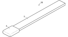
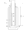
- FIG. 1 is a schematic external perspective view of a sensor element (gas sensor element) 10 according to an embodiment of the present invention.
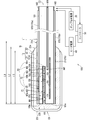
- FIG. 2 is a schematic view of the configuration of the gas sensor 100 including a cross-sectional view taken along the longitudinal direction of the sensor element 10.
- the sensor element 10 is a ceramic structure which is a main component of the gas sensor 100 which detects a predetermined gas component in the gas to be measured and measures the concentration thereof.
- the sensor element 10 is a so-called limit current type gas sensor element.
- the gas sensor 100 mainly includes a pump cell power supply 30, a heater power supply 40, and a controller 50.
- the sensor element 10 generally has a structure in which one end side of a long plate-shaped element substrate 1 is covered with a porous tip protective layer 2.
- the tip protection layer 2 is composed of three layers: a first tip protection layer 21, a second tip protection layer 22, and a third tip protection layer 23. Details of the tip protection layer 2 will be described later.
- the element substrate 1 has a long plate-shaped ceramic body 101 as a main structure, and a main surface protective layer 170 is provided on the two main surfaces of the ceramic body 101.
- the tip protective layer 2 is provided on the end surface on the one tip side (the tip surface 101e of the ceramic body 101) and on the outside of the four side surfaces.
- the four side surfaces of the sensor element 10 (or the element base 1, the ceramic body 101) excluding both end faces in the longitudinal direction are simply referred to as side surfaces of the sensor element 10 (or the element base 1, the ceramic body 101). ..
- the ceramic body 101 is made of ceramics containing zirconia (yttrium-stabilized zirconia), which is an oxygen ion conductive solid electrolyte, as a main component. Further, various components of the sensor element 10 are provided inside and outside the ceramic body 101. The ceramic body 101 having such a structure is dense and airtight.
- the configuration of the sensor element 10 shown in FIG. 2 is merely an example, and the specific configuration of the sensor element 10 is not limited to this.
- the sensor element 10 shown in FIG. 2 is a so-called series three-chamber structure type gas sensor element having a first internal vacancy 102, a second internal vacancy 103, and a third internal vacancy 104 inside the ceramic body 101.
- the first internal vacancy 102 is a gas that opens to the outside on the one end E1 side of the ceramic body 101 (strictly speaking, communicates with the outside via the tip protection layer 2). It communicates with the introduction port 105 through the first diffusion-controlled unit 110 and the second diffusion-controlled unit 120, and the second internal vacancy 103 communicates with the first internal vacancy 102 through the third diffusion-controlled unit 130.
- the third internal vacancy 104 communicates with the second internal vacancy 103 through the fourth diffusion-controlled unit 140.
- the route from the gas introduction port 105 to the third internal vacant room 104 is also referred to as a gas distribution unit.
- the gas flow portion is provided in a straight line along the longitudinal direction of the ceramic body 101.
- the first diffusion-controlled unit 110, the second diffusion-controlled unit 120, the third diffusion-controlled unit 130, and the fourth diffusion-controlled unit 140 are all provided as two slits at the top and bottom of the drawing.
- the first diffusion-controlled unit 110, the second diffusion-controlled unit 120, the third diffusion-controlled unit 130, and the fourth diffusion-controlled unit 140 impart a predetermined diffusion resistance to the passing gas to be measured.
- a buffer space 115 having an effect of buffering the pulsation of the gas to be measured is provided between the first diffusion-controlled unit 110 and the second diffusion-controlled unit 120.
- the outer surface of the ceramic body 101 is provided with the external pump electrode 141, and the first internal vacancy 102 is provided with the internal pump electrode 142. Further, the second internal vacancy 103 is provided with an auxiliary pump electrode 143, and the third internal vacancy 104 is provided with a measurement electrode 145 which is a direct detection unit for the gas component to be measured.
- the other end E2 side of the ceramic body 101 is provided with a reference gas introduction port 106 through which the reference gas is introduced to the outside, and a reference electrode 147 is provided in the reference gas introduction port 106. Has been done.
- the NOx gas concentration in the gas to be measured is calculated by the following process.
- the gas to be measured introduced into the first internal vacancy 102 has an oxygen concentration adjusted to be substantially constant by the pumping action (pumping or pumping out oxygen) of the main pump cell P1, and then the second interior. It is introduced in the vacant room 103.
- the main pump cell P1 is an electrochemical pump cell composed of an external pump electrode 141, an internal pump electrode 142, and a ceramic layer 101a which is a portion of a ceramic body 101 existing between the two electrodes.
- oxygen in the gas to be measured is pumped out to the outside of the element by the pumping action of the auxiliary pump cell P2, which is also an electrochemical pump cell, and the gas to be measured is sufficiently low oxygen. It is in a divided state.
- the auxiliary pump cell P2 is composed of an external pump electrode 141, an auxiliary pump electrode 143, and a ceramic layer 101b which is a portion of a ceramic body 101 existing between the two electrodes.
- the external pump electrode 141, the internal pump electrode 142, and the auxiliary pump electrode 143 are formed as a porous cermet electrode (for example, a cermet electrode of Pt containing 1% Au and ZrO 2 ).
- the internal pump electrode 142 and the auxiliary pump electrode 143 that come into contact with the gas to be measured are formed by using a material having a weakened or non-reducing ability to the NOx component in the gas to be measured.
- the measurement electrode 145 is a porous cermet electrode that also functions as a NOx reduction catalyst that reduces NOx existing in the atmosphere in the third internal vacancy 104.
- the potential difference between the measurement electrode 145 and the reference electrode 147 is kept constant. Then, the oxygen ions generated by the above-mentioned reduction or decomposition are pumped out of the device by the measurement pump cell P3.
- the measurement pump cell P3 is composed of an external pump electrode 141, a measurement electrode 145, and a ceramic layer 101c which is a portion of a ceramic body 101 existing between the two electrodes.
- the measurement pump cell P3 is an electrochemical pump cell that pumps out oxygen generated by decomposition of NOx in the atmosphere around the measurement electrode 145.
- Pumping (pumping or pumping oxygen) in the main pump cell P1, the auxiliary pump cell P2, and the measuring pump cell P3 is pumped between the electrodes provided in each pump cell by the pump cell power supply (variable power supply) 30 under the control of the controller 50. It is realized by applying the voltage required for. In the case of the measurement pump cell P3, a voltage is applied between the external pump electrode 141 and the measurement electrode 145 so that the potential difference between the measurement electrode 145 and the reference electrode 147 is maintained at a predetermined value. ..
- the pump cell power supply 30 is usually provided for each pump cell.
- the controller 50 detects the pump current Ip2 flowing between the measurement electrode 145 and the external pump electrode 141 according to the amount of oxygen pumped by the measurement pump cell P3, and determines the current value (NOx signal) of the pump current Ip2. , The NOx concentration in the gas to be measured is calculated based on the linear relationship with the concentration of the decomposed NOx.
- the gas sensor 100 includes a plurality of electrochemical sensor cells (not shown) that detect a potential difference between each pump electrode and the reference electrode 147, and the controller 50 controls each pump cell. It is performed based on the detection signal of the sensor cell.
- the heater 150 is embedded inside the ceramic body 101.
- the heater 150 is provided on the lower side of the gas flow section in FIG. 2 as viewed from the drawing, over a range from the vicinity of one end E1 to at least the formation positions of the measurement electrode 145 and the reference electrode 147.
- the heater 150 is provided mainly for the purpose of heating the sensor element 10 in order to increase the oxygen ion conductivity of the solid electrolyte constituting the ceramic body 101 when the sensor element 10 is used. More specifically, the heater 150 is provided so as to be surrounded by an insulating layer 151.
- the heater 150 is a resistance heating element made of, for example, platinum.
- the heater 150 generates heat by supplying power from the heater power supply 40 under the control of the controller 50.
- the sensor element 10 is heated by the heater 150 so that the temperature in the range from at least the first internal vacancy 102 to the second internal vacancy 103 is 500 ° C. or higher.
- the entire gas distribution section from the gas introduction port 105 to the third internal vacant room 104 may be heated to 500 ° C. or higher. These are for increasing the oxygen ion conductivity of the solid electrolyte constituting each pump cell so that the capacity of each pump cell can be suitably exhibited.
- the temperature in the vicinity of the first internal vacancy 102 which is the highest temperature, is about 700 ° C. to 800 ° C.
- the set heating temperature of the heater 150 when driving the sensor element 10 is also referred to as an element driving temperature.
- the outer surface of the sensor element 10 provided with the main surface) is referred to as a pump surface
- the main surface on the side provided with the heater 150 (or the outer surface of the sensor element 10 provided with the main surface) located below the drawing in FIG. 2 is the heater surface. It may be called.
- the pump surface is the main surface of the gas inlet 105, the three internal vacant rooms, and the side closer to each pump cell than the heater 150
- the heater surface is the gas inlet 105, the three internal vacant rooms.
- a plurality of electrode terminals 160 for making an electrical connection between the sensor element 10 and the outside are formed on the other end E2 side on each main surface of the ceramic body 101. These electrode terminals 160 pass through a lead wire (not shown) provided inside the ceramic body 101, and have a predetermined correspondence relationship with the above-mentioned five electrodes, both ends of the heater 150, and a lead wire for detecting heater resistance (not shown). It is electrically connected. Therefore, the voltage is applied from the pump cell power supply 30 to each pump cell of the sensor element 10 and the heater 150 is heated by the power supply from the heater power supply 40 through the electrode terminal 160.
- the main surface protective layers 170 (170a, 170b) described above are provided on the pump surface and the heater surface of the ceramic body 101.
- the main surface protective layer 170 is a layer made of alumina, having a thickness of about 5 ⁇ m to 30 ⁇ m and having pores having a porosity of about 20% to 40%, and is a layer having pores on the main surface (pump surface and pump surface) of the ceramic body 101. It is provided for the purpose of preventing foreign matter and toxic substances from adhering to the heater surface) and the external pump electrode 141 provided on the pump surface side. Therefore, the main surface protective layer 170a on the pump surface side also functions as a pump electrode protective layer that protects the external pump electrode 141.
- the porosity is determined by applying a known image processing method (binarization, etc.) to the SEM (scanning electron microscope) image of the evaluation target.
- the main surface protective layer 170 is provided over substantially the entire surface of the pump surface and the heater surface except that a part of the electrode terminal 160 is exposed, but this is merely an example, and is more than the case shown in FIG.
- the main surface protection layer 170 may be provided unevenly in the vicinity of the external pump electrode 141 on the one end E1 side.
- the tip protection layer 2 is provided on the outermost peripheral portion within a predetermined range from one end portion E1 of the element substrate 1 having the above-described configuration.
- the tip protective layer 2 is provided by surrounding a portion of the element substrate 1 that becomes hot (up to about 700 ° C. to 800 ° C.) when the gas sensor 100 is used, thereby ensuring water resistance in the portion. This is to prevent cracks (water-covered cracks) from occurring in the element substrate 1 due to thermal shock caused by a local temperature drop due to the portion being directly exposed to water.
- the tip protective layer 2 is provided to prevent toxic substances such as Mg from entering the inside of the sensor element 10 and to ensure toxicity resistance.
- the configuration of the tip protection layer 2 is determined in consideration of ensuring the rapid temperature rise property.
- the tip protection layer 2 is the first tip protection layer 21, the second tip protection layer 22, and the third tip protection layer 23. It is composed of three layers.
- the first tip protective layer 21 is provided below to ensure adhesiveness (adhesion) between the second tip protective layer 22 (further, the third tip protective layer 23) formed on the first tip protective layer 21 and the element substrate 1. It is a stratum.
- the first tip protective layer 21 is provided on at least two main surfaces of the element substrate 1 on the pump surface side and the heater surface side. That is, the first tip protection layer 21 includes a first tip protection layer 21a on the pump surface side and a first tip protection layer 21b on the heater surface side.
- the first tip protective layer 21 is not provided on the tip surface 101e (of the element substrate 1) and the side surface of the ceramic body 101. This is to ensure adhesion, reduce the binding force on the element substrate 1, and prevent the rapid temperature rise from being impaired.
- the first tip protective layer 21 is made of alumina and has a porosity of 40% or more and a thickness of 20 ⁇ m to 60 ⁇ m. As will be described later, the first tip protective layer 21 is formed together with the element substrate 1 in the process of manufacturing the element substrate 1, unlike the second tip protective layer 22 and the third tip protective layer 23. Preferably, the porosity of the first tip protective layer 21 is 40% or more and 60% or less.
- the second tip protective layer 22 and the third tip protective layer 23 cover the tip surface 101e on the one tip E1 side of the element substrate 1 and the four side surfaces (on the outer periphery of the one tip E1 side of the element substrate 1). ), It is provided in order from the inside.
- the portion on the tip surface 101e side is particularly referred to as the tip portion 221 and the portion on the pump surface side and the heater surface side is particularly referred to as the main surface portion 222.
- the portion on the tip surface 101e side is particularly referred to as the tip portion 231
- the portions on the pump surface side and the heater surface side are particularly referred to as the main surface portion 232.
- the second tip protective layer 22 is made of alumina so as to have a porosity of 20% or more and a thickness of 200 ⁇ m to 800 ⁇ m.
- the second tip protective layer 22 has a porosity of 40% to 80%.
- the third tip protective layer 23 is made of alumina and has a thickness of 100 ⁇ m to 400 ⁇ m and a porosity of 10% to 35%, which is smaller than the porosity of the second tip protective layer 22. It is provided so as to be.
- the second tip protection layer 22 having the lowest thermal conductivity among the three layers has a smaller porosity than the second tip protection layer 22 provided on the outermost side.
- the third tip protective layer 23 is coated.
- the second tip protective layer 22 has a function (heat insulating effect) of suppressing heat conduction from the outside to the element substrate 1 by being provided as a layer having a low thermal conductivity
- the third tip protective layer 23 Has a function of maintaining the overall strength and a function of suppressing the infiltration of water into the inside.
- the second tip protective layer 22 and the third tip protective layer 23 are provided so as to satisfy the above-mentioned thickness and porosity ranges, so that the sensor element 10 rises during driving. Temperature performance (rapid temperature rise performance) is also ensured. That is, the sensor element 10 according to the present embodiment has two different characteristics, that is, the provision of heat and shock resistance (water resistance) and the securing of temperature rise performance.
- the temperature rising performance of the sensor element 10 means that the heater 150 provided inside the sensor element 10 starts heating the entire sensor element 10 including the tip protective layer 2 in order to start using the gas sensor 100. After that, the evaluation can be performed by the time until the sensor element 10 reaches a predetermined temperature (for example, the time until the heater 150 reaches the element drive temperature).
- the thickness of the second tip protective layer 22 is preferably 700 ⁇ m or less, and the thickness of the third tip protective layer 23 is preferably 300 ⁇ m or less.
- the second tip protective layer 22 and the third tip protective layer 23 are obtained by sequentially spraying (plasma spraying) their constituent materials onto the device substrate 1 on which the first tip protective layer 21 is formed on the surface. It is formed. This causes an anchor effect between the first tip protective layer 21 and the second tip protective layer 22 which are formed in advance with the production of the element substrate 1, and the first tip protective layer 21 is formed (formed on the outside). This is to ensure the adhesiveness (adhesion) of the second tip protective layer 22 (including the tip protective layer 23). In other words, this means that the first tip protective layer 21 has a function of ensuring adhesiveness (adhesion) with the second tip protective layer 22. By ensuring the adhesiveness (adhesiveness) in such an embodiment, the peeling of the tip protective layer 2 from the element substrate 1 due to the thermal shock due to the adhesion of water droplets is suitably suppressed.
- the water that has adhered to and condensed on the tip protective layer 2 during use and has entered the inside thereof raises the temperature of the sensor element 10 when the use is started again.
- the peeling of the tip protective layer 2 (hereinafter, peeling during evaporation) caused by the pressure increase inside the tip protective layer 2 caused by evaporation due to the evaporation is preferably suppressed.
- the third tip protective layer 23 has a function of suppressing the intrusion of water into the sensor element 10, but the third tip protective layer 23 As long as is a porous layer, it is difficult to completely block the infiltration of water into the inside of the tip protection layer 2, and some intrusion may occur.
- the above-mentioned peeling during evaporation is a phenomenon caused by water that has entered the inside of the tip protection layer 2 in this way.
- the arrangement range of the first tip protection layer 21, the second tip protection layer 22, and the third tip protection layer 23 constituting the tip protection layer 2 in the element longitudinal direction is preferably determined. As a result, peeling during such evaporation is suitably suppressed.
- the tip surface 101e (end surface of the element substrate 1) of the first tip protection layer 21, the second tip protection layer 22, and the third tip protection layer 23 is used as a starting point.
- the extending length in the element longitudinal direction is the first layer length L1, the second layer length L2, and the third layer length L3, respectively.
- the first tip protection layer 21, the second tip protection layer 22, and the third tip protection layer 23 are provided so as to satisfy the conditional expression.
- the formula (1) is formed in such a manner that the tip protection layer 2 exposes at least the end surface 21e of the first tip protection layer 21 opposite to the one end E1 side in the longitudinal direction of the sensor element 10. Means that.
- the third tip protective layer 23 surrounds at least a range of 500 ° C. or higher in the element substrate 1 when the sensor element 10 is driven (when the heater 150 is heated at the element driving temperature). It is provided to do so.
- the range is usually predetermined at the time of designing the sensor element 10. Further, the range includes at least the position from the tip surface 101e of the ceramic body 101 to the innermost position of the third internal vacancy 104 in the longitudinal direction of the element.
- the portion of the tip protection layer 2 having a high porosity is external.
- a configuration that directly communicates with is realized.
- the water vapor does not stay inside the tip protection layer 2 and is relatively easily outside mainly from a portion having a high porosity. Will be discharged to.
- the increase in water vapor pressure and the resulting peeling during evaporation are less likely to occur.
- the first tip protection layer 21, the second tip protection layer 22, and the third tip protection layer 23 are L1 ⁇ L2 ⁇ L3 ⁇ ⁇ ⁇ ⁇ (2) It may be provided so as to satisfy the conditional expression.
- FIG. 2 illustrates a case where the equation (2) is satisfied (more specifically, a case where L1>L2> L3).
- the end face 22e of the second tip protection layer 22 is also exposed, and peeling is less likely to occur during evaporation.
- the first tip protection layer 21, the second tip protection layer 22, and the third tip protection layer 23 are L1 ⁇ L3 ⁇ L2 ⁇ ⁇ ⁇ ⁇ (3) It may be provided so as to satisfy the conditional expression.
- the end face 21e of the first tip protection layer 21 is exposed, the end face 22e of the second tip protection layer 22 is not exposed, so that the infiltration of water from the latter is suppressed and peeling is less likely to occur during evaporation. ..
- the tip protective layer 2 surrounding the portion of the element substrate 1 that becomes hot when the gas sensor 100 is used is the first tip protective layer 21 and the first.
- the first tip protection layer 21 and the second tip protection layer 22 have a three-layer structure of the tip protection layer 22 and the third tip protection layer 23, and each is provided with a predetermined porosity and thickness.
- the second tip protective layer 22 has a function of suppressing heat conduction from the outside to the element substrate 1, and the third tip protective layer 23 has the function of ensuring the adhesiveness (adhesion) with the device. It has a function of maintaining the temperature and a function of suppressing the ingress of water into the inside. As a result, in the sensor element 10, it is possible to achieve both thermal shock resistance and temperature rise performance while ensuring the adhesion of the tip protective layer.
- the tip generated by the water that has entered the inside of the sensor element 10 evaporates as the temperature of the sensor element 10 rises. Peeling of the protective layer 2 during evaporation is suitably suppressed.
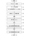
- FIG. 3 is a diagram showing a processing flow when manufacturing the sensor element 10.
- a plurality of blank sheets which are green sheets containing an oxygen ion conductive solid electrolyte such as zirconia as a ceramic component and have no pattern formed, are prepared (not shown). Step S1).
- the blank sheet is provided with a plurality of sheet holes used for positioning during printing and laminating.
- the sheet holes are formed in advance by punching with a punching device or the like at the stage of the blank sheet prior to pattern formation.
- the penetrating portion corresponding to the internal space is also provided in advance by the same punching process or the like.
- the thickness of each blank sheet does not have to be the same, and the thickness may be different depending on the corresponding portion of the finally formed element substrate 1.
- step S2 When a blank sheet corresponding to each layer is prepared, pattern printing / drying processing is performed on each blank sheet (step S2). Specifically, various electrode patterns, heater 150 and insulating layer 151 patterns, electrode terminal 160 patterns, main surface protection layer 170 patterns, internal wiring patterns (not shown), and the like are included. It is formed. Further, at the timing of the pattern printing, a sublimable material for forming the first diffusion-controlled unit 110, the second diffusion-controlled unit 120, the third diffusion-controlled unit 130, and the fourth diffusion-controlled unit 140 ( The disappearing material) is also applied or placed. In addition, a pattern for forming the first tip protective layer 21 (21a, 21b) is printed on the blank sheet which becomes the uppermost layer and the lowermost layer after laminating (step S2a).
- Printing of each pattern is performed by applying a pattern forming paste prepared according to the characteristics required for each forming target to a blank sheet using a known screen printing technique.
- a pattern forming paste prepared according to the characteristics required for each forming target to a blank sheet using a known screen printing technique.
- an alumina paste capable of forming the first tip protective layer 21 having a desired porosity and thickness in the finally obtained sensor element 10 is used.
- Known drying means can also be used for the drying treatment after printing.
- step S3 the adhesive paste for laminating and adhering the green sheets is printed and dried.
- a known screen printing technique can be used for printing the adhesive paste, and a known drying means can also be used for the drying treatment after printing.
- the green sheets coated with the adhesive are stacked in a predetermined order and crimped by applying predetermined temperature and pressure conditions to form a single laminate (step S4).
- the green sheets to be laminated are stacked and held on a predetermined laminating jig (not shown) while being positioned by the sheet holes, and the laminating jig is heated and pressurized by a laminating machine such as a known hydraulic press. Do by.
- the pressure, temperature, and time for heating and pressurizing depend on the laminating machine used, but appropriate conditions may be set so that good laminating can be achieved.
- a pattern for forming the first tip protective layer 21 may be formed on the laminate obtained in the above aspect.
- step S5 When the laminated body is obtained as described above, subsequently, a plurality of parts of the laminated body are cut, and each is cut into a unit body which finally becomes an individual element substrate 1 (step S5).
- the obtained unit body is fired at a firing temperature of about 1300 ° C. to 1500 ° C. (step S6).
- the device substrate 1 having the first tip protective layer 21 on both main surfaces is produced. That is, the element substrate 1 is generated by integrally firing the ceramic body 101 made of a solid electrolyte, each electrode, and the main surface protective layer 170 together with the first tip protective layer 21.
- each electrode has sufficient adhesion strength by being integrally fired in such an embodiment.
- the second tip protective layer 22 and the third tip protective layer 23 are subsequently formed on the device base 1.
- the second tip protective layer 22 is formed by applying a powder (alumina powder) for forming the second tip protective layer prepared in advance to the target position of the second tip protective layer 22 on the element substrate 1 according to the target formation thickness. After thermal spraying (step S7), the element substrate 1 on which the coating film is formed is fired (step S8) in such an embodiment.
- the alumina powder for forming the second tip protective layer contains the alumina powder having a predetermined particle size distribution and the pore-forming material in a ratio corresponding to the desired porosity, and the element substrate 1 is fired after thermal spraying.
- the second tip protective layer 22 having a high porosity of 40% to 80% is suitably formed by thermally decomposing the pore-forming material. It should be noted that known techniques can be applied to thermal spraying and firing.
- a powder (alumina powder) for forming the third tip protective layer which is also prepared in advance and contains alumina powder having a predetermined particle size distribution, is applied to the element substrate 1.
- the third tip protective layer 23 having a desired porosity is formed by spraying the target position of the third tip protective layer 23 according to the target formation thickness (step S9).
- the alumina powder for forming the third tip protective layer does not contain a pore-forming material. Known techniques can also be applied to such thermal spraying.
- the sensor element 10 can be obtained by the above procedure.
- the obtained sensor element 10 is housed in a predetermined housing and incorporated into the main body (not shown) of the gas sensor 100.
- the first tip protection layer 21, the second tip protection layer 22, and the third tip protection layer 23 are provided so as to satisfy the formula (1) or further the formula (2) or the formula (3).
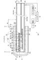
- 4 and 5 are schematic views of the configuration of the gas sensor 100 including a cross-sectional view of the sensor element 10 according to the modified example along the longitudinal direction based on this.
- the sensor element having three internal vacancies is targeted, but it is not essential that the sensor element has a three-chamber structure. That is, the sensor element may have two or one internal vacancies.
- step S7 after the powder for forming the second tip protective layer is sprayed in step S7, the powder is fired in step S8, and then the powder for forming the third tip protective layer is sprayed in step S9.
- step S8 and thermal spraying in step S9 may be interchanged.
- the second tip protective layer 22 and the third tip protective layer 23 are provided with alumina, and alumina powder is used as the thermal spray material when forming both layers.
- alumina powder is used as the thermal spray material when forming both layers.
- metal oxides such as zirconia (ZrO 2 ), spinel (MgAl 2 O 4 ), and mullite (Al 6 O 13 Si 2 ) are used to protect the second tip protective layer 22 and the third tip protective layer 23. May be provided.
- the powder of those metal oxides may be adopted as a thermal spraying material.
- first layer the first tip protective layer
- second layer the second tip protection layer
- third layer the third tip protection layer
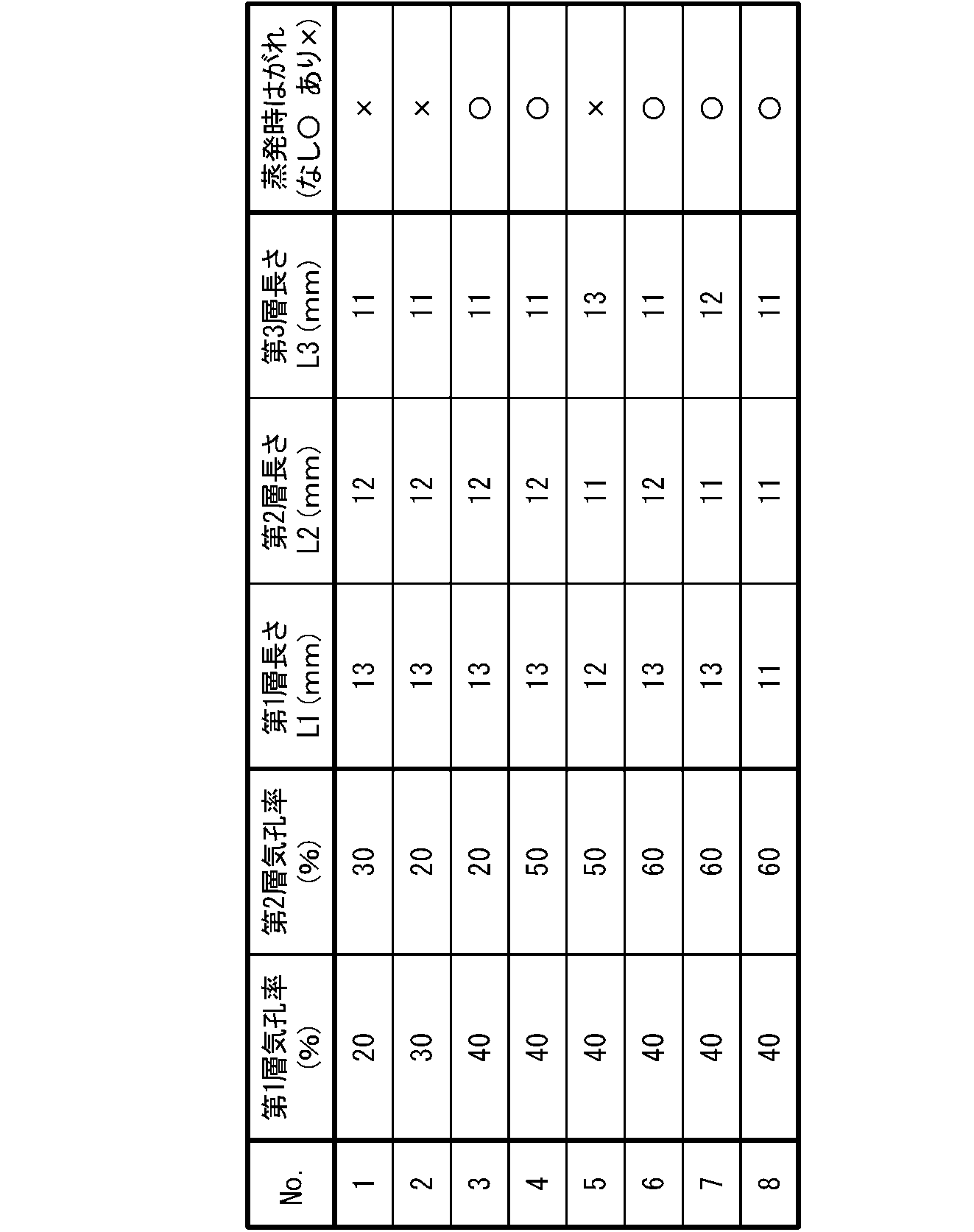
- Sensor elements 10 (Sample Nos. 1 to 8) were produced.
- the first layer 21, the second layer 22, and the third layer 23 are all made of alumina, and the porosity of the first layer 21 and the second layer 22 is determined.
- the combination of the first layer length L1, the second layer length L2, and the third layer length L3 was different for each.
- the porosity of the third layer 23 was 25%, and the thicknesses of the first layer 21, the second layer 22, and the third layer 23 were 40 ⁇ m, 500 ⁇ m, and 200 ⁇ m, respectively.
- the porosities of the first layer 21 and the second layer 22 in each sensor element 10 and the first layer length L1, the second layer length L2, and the third layer length L3 are shown in Table 1 below. Shown in a list. In such a case, No. 1 to No. 4 and No. 6-No. The sample of 8 satisfies the formula (1). In addition, No. 1 to No. 4 and No. The sample of 6 satisfies the formula (2) in addition to the formula (1). On the other hand, No. The sample of No. 7 satisfies the formula (3) in addition to the formula (1). In addition, No. The sample of 8 has the structure shown in FIG.
- the minimum values of the first layer length L1, the second layer length L2, and the third layer length L3 are 11 mm, but the temperature is 500 ° C. or higher when driven. It is common in that the range is surrounded by the tip protection layer 2.
- the produced No. 1 to No. The temperature rising performance was evaluated for the sensor element 10 of 8.
- the temperature rising performance is the length of the time (heating time) from the start of driving the sensor element 10 at room temperature until the temperature of the sensor element 10 reaches 850 ° C., which is assumed as the element driving temperature. Evaluated at.
- the temperature of the sensor element 10 was calculated from the resistance value inside the element.
- the temperature rising time is 30 seconds or less, the temperature rising time is 30 seconds or less in any of the sensor elements 10. That is, each of the sensor elements 10 had the required temperature raising performance.
- sample No. 1 to No. The adhesion of the tip protection layer 2 was evaluated for the sensor element 10 of 8. The adhesion was evaluated by the magnitude of the force required to displace the element substrate 1 by pulling only the element substrate 1 in the longitudinal direction with the tip protective layer 2 fixed.
- the force required to displace the element substrate 1 is 100 N or more, it can be determined that there is no problem in adhesion. However, the force is 100 N or more in any of the sensor elements 10. That is, each of the sensor elements 10 had the necessary adhesion to the tip protection layer 2.
- sample No. 1 to No. The sensor element 10 of No. 8 was evaluated for peeling during evaporation of the tip protection layer 2.
- the sensor element 10 at room temperature immersed in water for a sufficient time is taken out of the water and heated by the heater 150 to evaporate the water, and then the cross section of the sensor element 10 after heating. was observed by SEM.
- the immersion of the sensor element 10 in water in such a case is a process in which water is much more likely to enter the tip protective layer 2 than in the normal use of the gas sensor 100.
- the porosity of the first layer 21 is at least 40%, and the relationship between the first layer length L1, the second layer length L2, and the third layer length L3 is at least the relation of the formula (1).
- the sensor element 10 in which the occurrence of peeling during evaporation is suitably suppressed is realized.
Landscapes
- Chemical & Material Sciences (AREA)
- Life Sciences & Earth Sciences (AREA)
- Health & Medical Sciences (AREA)
- Biochemistry (AREA)
- Chemical Kinetics & Catalysis (AREA)
- Electrochemistry (AREA)
- Physics & Mathematics (AREA)
- Analytical Chemistry (AREA)
- Molecular Biology (AREA)
- General Health & Medical Sciences (AREA)
- General Physics & Mathematics (AREA)
- Immunology (AREA)
- Pathology (AREA)
- Measuring Oxygen Concentration In Cells (AREA)
- Details Of Resistors (AREA)
- Non-Adjustable Resistors (AREA)
Abstract
Description
図1は、本発明の実施の形態に係るセンサ素子(ガスセンサ素子)10の概略的な外観斜視図である。また、図2は、センサ素子10の長手方向に沿った断面図を含むガスセンサ100の構成の概略図である。センサ素子10は、被測定ガス中の所定ガス成分を検知しその濃度を測定するガスセンサ100の、主たる構成要素であるセラミックス構造体である。センサ素子10は、いわゆる限界電流型のガスセンサ素子である。
センサ素子10においては、上述のような構成を有する素子基体1の一方端部E1から所定範囲の最外周部に、先端保護層2が設けられてなる。
L1≧L2かつL1≧L3 ・・・・(1)
なる条件式を満たすように、第1先端保護層21、第2先端保護層22、および第3先端保護層23が設けられる。
L1≧L2≧L3 ・・・・(2)
なる条件式を満たすように、設けられてもよい。図2には、係る式(2)を充足する場合(より詳細にはL1>L2>L3の場合)が、例示されている。この場合、第1先端保護層21の端面21eに加えて第2先端保護層22の端面22eも露出することとなり、蒸発時はがれがさらに生じにくくなる。
L1≧L3≧L2 ・・・・(3)
なる条件式を満たすように、設けられてもよい。この場合、第1先端保護層21の端面21eは露出するものの、第2先端保護層22の端面22eは露出しないため、後者からの水の浸入が抑制され、かつ、蒸発時はがれが生じにくくなる。
次に、上述のような構成および特徴を有するセンサ素子10を製造するプロセスの一例について説明する。図3は、センサ素子10を作製する際の処理の流れを示す図である。
上述したように、第1先端保護層21、第2先端保護層22、および第3先端保護層23は、式(1)あるいはさらに式(2)または式(3)を満たすように、設けられればよい。図4および図5は、これを踏まえた、変形例に係るセンサ素子10の長手方向に沿った断面図を含むガスセンサ100の構成の概略図である。
Claims (6)
- ガスセンサのセンサ素子であって、
測定対象ガス成分の検知部を備えたセラミックス構造体である素子基体と、
前記素子基体のうち、前記検知部が備わる側の端部から所定範囲の外周部に設けられた多孔質層である先端保護層と、
を備え、
前記先端保護層が、
前記素子基体の2つの主面上に設けられてなる第1先端保護層と、
前記端部と、前記第1先端保護層が形成されてなる前記2つの主面を含む前記素子基体の4つの側面とを覆うように設けられてなる第2先端保護層と、
前記第2先端保護層を覆うように設けられてなり、前記第2先端保護層よりも気孔率が小さい第3先端保護層と、
からなり、
前記第1先端保護層が40%以上の気孔率を有してなり、
前記素子基体の長手方向における、前記素子基体の端面を起点とした前記第1先端保護層、前記第2先端保護層、および前記第3先端保護層の延在長さをそれぞれL1、L2、およびL3とするとき、
L1≧L2かつL1≧L3
である、
ことを特徴とする、ガスセンサのセンサ素子。 - 請求項1に記載のセンサ素子であって、
L1≧L2≧L3
である、
ことを特徴とする、ガスセンサのセンサ素子。 - 請求項1に記載のセンサ素子であって、
L1≧L3≧L2
である、
ことを特徴とする、ガスセンサのセンサ素子。 - 請求項1ないし請求項3のいずれかに記載のセンサ素子であって、
前記第2先端保護層の気孔率が40%~80%である、
ことを特徴とする、ガスセンサのセンサ素子。 - 請求項1ないし請求項4のいずれかに記載のセンサ素子であって、
前記第1先端保護層の気孔率が40%~60%である、
ことを特徴とする、ガスセンサのセンサ素子。 - 請求項1ないし請求項5のいずれかに記載のセンサ素子であって、
前記第3先端保護層が、前記センサ素子の素子基体のうち、あらかじめ特定された、駆動時に500℃以上となる範囲を少なくとも囲繞する、
ことを特徴とする、ガスセンサのセンサ素子。
Priority Applications (4)
| Application Number | Priority Date | Filing Date | Title |
|---|---|---|---|
| JP2021511291A JP7060761B2 (ja) | 2019-03-29 | 2020-03-06 | ガスセンサのセンサ素子 |
| DE112020001640.4T DE112020001640T5 (de) | 2019-03-29 | 2020-03-06 | Sensorelement eines Gassensors |
| CN202080017366.3A CN113597552B (zh) | 2019-03-29 | 2020-03-06 | 气体传感器的传感器元件 |
| US17/460,780 US20210389271A1 (en) | 2019-03-29 | 2021-08-30 | Sensor element of gas sensor |
Applications Claiming Priority (2)
| Application Number | Priority Date | Filing Date | Title |
|---|---|---|---|
| JP2019066549 | 2019-03-29 | ||
| JP2019-066549 | 2019-03-29 |
Related Child Applications (1)
| Application Number | Title | Priority Date | Filing Date |
|---|---|---|---|
| US17/460,780 Continuation US20210389271A1 (en) | 2019-03-29 | 2021-08-30 | Sensor element of gas sensor |
Publications (1)
| Publication Number | Publication Date |
|---|---|
| WO2020203029A1 true WO2020203029A1 (ja) | 2020-10-08 |
Family
ID=72668671
Family Applications (1)
| Application Number | Title | Priority Date | Filing Date |
|---|---|---|---|
| PCT/JP2020/009601 Ceased WO2020203029A1 (ja) | 2019-03-29 | 2020-03-06 | ガスセンサのセンサ素子 |
Country Status (5)
| Country | Link |
|---|---|
| US (1) | US20210389271A1 (ja) |
| JP (1) | JP7060761B2 (ja) |
| CN (1) | CN113597552B (ja) |
| DE (1) | DE112020001640T5 (ja) |
| WO (1) | WO2020203029A1 (ja) |
Cited By (2)
| Publication number | Priority date | Publication date | Assignee | Title |
|---|---|---|---|---|
| DE102024104024A1 (de) | 2023-03-27 | 2024-10-02 | Ngk Insulators, Ltd. | Sensorelement |
| DE102024104074A1 (de) | 2023-03-27 | 2024-10-02 | Ngk Insulators, Ltd. | Sensorelement |
Families Citing this family (1)
| Publication number | Priority date | Publication date | Assignee | Title |
|---|---|---|---|---|
| JP7265558B2 (ja) * | 2018-10-03 | 2023-04-26 | 日本碍子株式会社 | センサ素子 |
Citations (4)
| Publication number | Priority date | Publication date | Assignee | Title |
|---|---|---|---|---|
| JP2012189579A (ja) * | 2011-02-22 | 2012-10-04 | Ngk Spark Plug Co Ltd | ガスセンサ素子及びガスセンサ |
| JP2018169324A (ja) * | 2017-03-30 | 2018-11-01 | 日本碍子株式会社 | ガスセンサ素子 |
| JP2020020738A (ja) * | 2018-08-03 | 2020-02-06 | 日本碍子株式会社 | センサ素子 |
| JP2020034443A (ja) * | 2018-08-30 | 2020-03-05 | 日本碍子株式会社 | センサ素子 |
Family Cites Families (8)
| Publication number | Priority date | Publication date | Assignee | Title |
|---|---|---|---|---|
| JPH05344375A (ja) | 1992-06-09 | 1993-12-24 | Victor Co Of Japan Ltd | ラスター歪補正回路 |
| JP5000984B2 (ja) * | 2006-11-06 | 2012-08-15 | 日本特殊陶業株式会社 | ガスセンサ |
| JP2009080099A (ja) * | 2007-09-07 | 2009-04-16 | Denso Corp | ガスセンサ素子及びその製造方法 |
| JP5322965B2 (ja) * | 2010-02-02 | 2013-10-23 | 日本碍子株式会社 | ガスセンサ及びその製造方法 |
| JP6488146B2 (ja) * | 2014-03-28 | 2019-03-20 | 日本碍子株式会社 | 被膜の製造方法及びガスセンサの製造方法 |
| JP6885760B2 (ja) * | 2016-03-30 | 2021-06-16 | 日本碍子株式会社 | センサ素子及びガスセンサ |
| JP2018009817A (ja) * | 2016-07-11 | 2018-01-18 | 株式会社デンソー | ガスセンサ |
| JP6761369B2 (ja) * | 2017-03-30 | 2020-09-23 | 日本碍子株式会社 | ガスセンサ素子 |
-
2020
- 2020-03-06 WO PCT/JP2020/009601 patent/WO2020203029A1/ja not_active Ceased
- 2020-03-06 CN CN202080017366.3A patent/CN113597552B/zh active Active
- 2020-03-06 DE DE112020001640.4T patent/DE112020001640T5/de active Pending
- 2020-03-06 JP JP2021511291A patent/JP7060761B2/ja active Active
-
2021
- 2021-08-30 US US17/460,780 patent/US20210389271A1/en active Pending
Patent Citations (4)
| Publication number | Priority date | Publication date | Assignee | Title |
|---|---|---|---|---|
| JP2012189579A (ja) * | 2011-02-22 | 2012-10-04 | Ngk Spark Plug Co Ltd | ガスセンサ素子及びガスセンサ |
| JP2018169324A (ja) * | 2017-03-30 | 2018-11-01 | 日本碍子株式会社 | ガスセンサ素子 |
| JP2020020738A (ja) * | 2018-08-03 | 2020-02-06 | 日本碍子株式会社 | センサ素子 |
| JP2020034443A (ja) * | 2018-08-30 | 2020-03-05 | 日本碍子株式会社 | センサ素子 |
Cited By (4)
| Publication number | Priority date | Publication date | Assignee | Title |
|---|---|---|---|---|
| DE102024104024A1 (de) | 2023-03-27 | 2024-10-02 | Ngk Insulators, Ltd. | Sensorelement |
| DE102024104074A1 (de) | 2023-03-27 | 2024-10-02 | Ngk Insulators, Ltd. | Sensorelement |
| JP2024139518A (ja) * | 2023-03-27 | 2024-10-09 | 日本碍子株式会社 | センサ素子 |
| JP7813743B2 (ja) | 2023-03-27 | 2026-02-13 | 日本碍子株式会社 | センサ素子 |
Also Published As
| Publication number | Publication date |
|---|---|
| CN113597552A (zh) | 2021-11-02 |
| JPWO2020203029A1 (ja) | 2020-10-08 |
| CN113597552B (zh) | 2025-03-11 |
| JP7060761B2 (ja) | 2022-04-26 |
| US20210389271A1 (en) | 2021-12-16 |
| DE112020001640T5 (de) | 2021-12-16 |
Similar Documents
| Publication | Publication Date | Title |
|---|---|---|
| JP7089990B2 (ja) | センサ素子 | |
| JP2020034435A (ja) | センサ素子 | |
| JP7082921B2 (ja) | センサ素子 | |
| CN108693235B (zh) | 传感器元件 | |
| JP7402297B2 (ja) | センサ素子 | |
| JP7060761B2 (ja) | ガスセンサのセンサ素子 | |
| JP7122248B2 (ja) | センサ素子 | |
| JP7265558B2 (ja) | センサ素子 | |
| JP7227824B2 (ja) | ガスセンサのセンサ素子 | |
| JP2020020742A (ja) | センサ素子 | |
| JP7090211B2 (ja) | ガスセンサのセンサ素子 | |
| US10739300B2 (en) | Sensor element | |
| US11592419B2 (en) | Sensor element for gas sensor | |
| JP7261640B2 (ja) | ガスセンサのセンサ素子 | |
| JP7179968B2 (ja) | ガスセンサのセンサ素子 | |
| JP7360311B2 (ja) | ガスセンサのセンサ素子 | |
| JP7194809B2 (ja) | ガスセンサのセンサ素子 | |
| JP6877219B2 (ja) | センサ素子 | |
| JPWO2020195692A1 (ja) | ガスセンサのセンサ素子 | |
| JP2021105567A (ja) | ガスセンサのセンサ素子 |
Legal Events
| Date | Code | Title | Description |
|---|---|---|---|
| 121 | Ep: the epo has been informed by wipo that ep was designated in this application |
Ref document number: 20785192 Country of ref document: EP Kind code of ref document: A1 |
|
| ENP | Entry into the national phase |
Ref document number: 2021511291 Country of ref document: JP Kind code of ref document: A |
|
| 122 | Ep: pct application non-entry in european phase |
Ref document number: 20785192 Country of ref document: EP Kind code of ref document: A1 |
|
| WWG | Wipo information: grant in national office |
Ref document number: 202080017366.3 Country of ref document: CN |