WO2020201860A1 - Circuit logique configuré à l'aide de transistors unipolaires, et dispositif à semi-conducteurs - Google Patents
Circuit logique configuré à l'aide de transistors unipolaires, et dispositif à semi-conducteurs Download PDFInfo
- Publication number
- WO2020201860A1 WO2020201860A1 PCT/IB2020/052186 IB2020052186W WO2020201860A1 WO 2020201860 A1 WO2020201860 A1 WO 2020201860A1 IB 2020052186 W IB2020052186 W IB 2020052186W WO 2020201860 A1 WO2020201860 A1 WO 2020201860A1
- Authority
- WO
- WIPO (PCT)
- Prior art keywords
- transistor
- drain
- source
- electrically connected
- oxide
- Prior art date
Links
- 239000004065 semiconductor Substances 0.000 title claims abstract description 292
- 229910044991 metal oxide Inorganic materials 0.000 claims description 134
- 150000004706 metal oxides Chemical class 0.000 claims description 126
- 239000012212 insulator Substances 0.000 description 515
- 239000004020 conductor Substances 0.000 description 475
- 239000010408 film Substances 0.000 description 144
- 230000006870 function Effects 0.000 description 141
- 239000001257 hydrogen Substances 0.000 description 106
- 229910052739 hydrogen Inorganic materials 0.000 description 106
- 229910052760 oxygen Inorganic materials 0.000 description 104
- QVGXLLKOCUKJST-UHFFFAOYSA-N atomic oxygen Chemical compound [O] QVGXLLKOCUKJST-UHFFFAOYSA-N 0.000 description 103
- 239000001301 oxygen Substances 0.000 description 103
- UFHFLCQGNIYNRP-UHFFFAOYSA-N Hydrogen Chemical compound [H][H] UFHFLCQGNIYNRP-UHFFFAOYSA-N 0.000 description 95
- 239000010410 layer Substances 0.000 description 95
- 239000000463 material Substances 0.000 description 79
- 239000012535 impurity Substances 0.000 description 68
- 230000004888 barrier function Effects 0.000 description 59
- 229910052814 silicon oxide Inorganic materials 0.000 description 52
- 238000009792 diffusion process Methods 0.000 description 50
- VYPSYNLAJGMNEJ-UHFFFAOYSA-N Silicium dioxide Chemical compound O=[Si]=O VYPSYNLAJGMNEJ-UHFFFAOYSA-N 0.000 description 45
- 239000011701 zinc Substances 0.000 description 41
- 239000013078 crystal Substances 0.000 description 40
- 229910052782 aluminium Inorganic materials 0.000 description 37
- XAGFODPZIPBFFR-UHFFFAOYSA-N aluminium Chemical compound [Al] XAGFODPZIPBFFR-UHFFFAOYSA-N 0.000 description 36
- 125000004429 atom Chemical group 0.000 description 33
- XLYOFNOQVPJJNP-UHFFFAOYSA-N water Substances O XLYOFNOQVPJJNP-UHFFFAOYSA-N 0.000 description 33
- 229910001868 water Inorganic materials 0.000 description 33
- 229910052721 tungsten Inorganic materials 0.000 description 30
- 239000010937 tungsten Substances 0.000 description 30
- 229910052581 Si3N4 Inorganic materials 0.000 description 29
- -1 for example Inorganic materials 0.000 description 29
- WFKWXMTUELFFGS-UHFFFAOYSA-N tungsten Chemical compound [W] WFKWXMTUELFFGS-UHFFFAOYSA-N 0.000 description 29
- 230000002829 reductive effect Effects 0.000 description 28
- HQVNEWCFYHHQES-UHFFFAOYSA-N silicon nitride Chemical compound N12[Si]34N5[Si]62N3[Si]51N64 HQVNEWCFYHHQES-UHFFFAOYSA-N 0.000 description 28
- IJGRMHOSHXDMSA-UHFFFAOYSA-N Atomic nitrogen Chemical compound N#N IJGRMHOSHXDMSA-UHFFFAOYSA-N 0.000 description 27
- TWNQGVIAIRXVLR-UHFFFAOYSA-N oxo(oxoalumanyloxy)alumane Chemical compound O=[Al]O[Al]=O TWNQGVIAIRXVLR-UHFFFAOYSA-N 0.000 description 25
- RYGMFSIKBFXOCR-UHFFFAOYSA-N Copper Chemical compound [Cu] RYGMFSIKBFXOCR-UHFFFAOYSA-N 0.000 description 24
- 230000008859 change Effects 0.000 description 23
- 229910052751 metal Inorganic materials 0.000 description 23
- 239000002184 metal Substances 0.000 description 22
- PXHVJJICTQNCMI-UHFFFAOYSA-N Nickel Chemical group [Ni] PXHVJJICTQNCMI-UHFFFAOYSA-N 0.000 description 20
- 239000010949 copper Substances 0.000 description 20
- 230000007547 defect Effects 0.000 description 20
- 229910052735 hafnium Inorganic materials 0.000 description 20
- 229910052802 copper Inorganic materials 0.000 description 19
- 238000010586 diagram Methods 0.000 description 18
- 238000000034 method Methods 0.000 description 18
- 239000000758 substrate Substances 0.000 description 18
- RTAQQCXQSZGOHL-UHFFFAOYSA-N Titanium Chemical group [Ti] RTAQQCXQSZGOHL-UHFFFAOYSA-N 0.000 description 17
- 230000015572 biosynthetic process Effects 0.000 description 17
- 229910052719 titanium Inorganic materials 0.000 description 17
- 239000010936 titanium Chemical group 0.000 description 17
- 230000003647 oxidation Effects 0.000 description 16
- 238000007254 oxidation reaction Methods 0.000 description 16
- 239000002356 single layer Substances 0.000 description 15
- VBJZVLUMGGDVMO-UHFFFAOYSA-N hafnium atom Chemical compound [Hf] VBJZVLUMGGDVMO-UHFFFAOYSA-N 0.000 description 14
- 229910000449 hafnium oxide Inorganic materials 0.000 description 14
- WIHZLLGSGQNAGK-UHFFFAOYSA-N hafnium(4+);oxygen(2-) Chemical compound [O-2].[O-2].[Hf+4] WIHZLLGSGQNAGK-UHFFFAOYSA-N 0.000 description 14
- 229910052757 nitrogen Inorganic materials 0.000 description 14
- NRTOMJZYCJJWKI-UHFFFAOYSA-N Titanium nitride Chemical compound [Ti]#N NRTOMJZYCJJWKI-UHFFFAOYSA-N 0.000 description 13
- 150000002431 hydrogen Chemical class 0.000 description 13
- ZOKXTWBITQBERF-UHFFFAOYSA-N Molybdenum Chemical compound [Mo] ZOKXTWBITQBERF-UHFFFAOYSA-N 0.000 description 12
- 239000011229 interlayer Substances 0.000 description 12
- 229910052750 molybdenum Inorganic materials 0.000 description 12
- 239000011733 molybdenum Substances 0.000 description 12
- MZLGASXMSKOWSE-UHFFFAOYSA-N tantalum nitride Chemical compound [Ta]#N MZLGASXMSKOWSE-UHFFFAOYSA-N 0.000 description 12
- OKTJSMMVPCPJKN-UHFFFAOYSA-N Carbon Chemical compound [C] OKTJSMMVPCPJKN-UHFFFAOYSA-N 0.000 description 11
- 230000005684 electric field Effects 0.000 description 11
- 229910052715 tantalum Inorganic materials 0.000 description 11
- GUVRBAGPIYLISA-UHFFFAOYSA-N tantalum atom Chemical compound [Ta] GUVRBAGPIYLISA-UHFFFAOYSA-N 0.000 description 11
- 206010021143 Hypoxia Diseases 0.000 description 10
- 229910052799 carbon Inorganic materials 0.000 description 10
- 230000007423 decrease Effects 0.000 description 10
- 229910052759 nickel Inorganic materials 0.000 description 10
- 230000000717 retained effect Effects 0.000 description 10
- 238000001228 spectrum Methods 0.000 description 10
- XUIMIQQOPSSXEZ-UHFFFAOYSA-N Silicon Chemical compound [Si] XUIMIQQOPSSXEZ-UHFFFAOYSA-N 0.000 description 9
- 239000000969 carrier Substances 0.000 description 9
- 239000000470 constituent Substances 0.000 description 9
- 238000010438 heat treatment Methods 0.000 description 9
- 238000004519 manufacturing process Methods 0.000 description 9
- 150000004767 nitrides Chemical class 0.000 description 9
- 125000004430 oxygen atom Chemical group O* 0.000 description 9
- 229910052710 silicon Inorganic materials 0.000 description 9
- 239000010703 silicon Substances 0.000 description 9
- 230000008878 coupling Effects 0.000 description 8
- 238000010168 coupling process Methods 0.000 description 8
- 238000005859 coupling reaction Methods 0.000 description 8
- 230000003071 parasitic effect Effects 0.000 description 8
- 239000012466 permeate Substances 0.000 description 8
- 238000001004 secondary ion mass spectrometry Methods 0.000 description 8
- 238000004544 sputter deposition Methods 0.000 description 8
- 239000000126 substance Substances 0.000 description 8
- 239000000956 alloy Substances 0.000 description 7
- 238000004458 analytical method Methods 0.000 description 7
- AJNVQOSZGJRYEI-UHFFFAOYSA-N digallium;oxygen(2-) Chemical compound [O-2].[O-2].[O-2].[Ga+3].[Ga+3] AJNVQOSZGJRYEI-UHFFFAOYSA-N 0.000 description 7
- 230000000694 effects Effects 0.000 description 7
- 229910001195 gallium oxide Inorganic materials 0.000 description 7
- 125000004435 hydrogen atom Chemical group [H]* 0.000 description 7
- 229910052738 indium Inorganic materials 0.000 description 7
- 239000011810 insulating material Substances 0.000 description 7
- 239000012528 membrane Substances 0.000 description 7
- 239000007769 metal material Substances 0.000 description 7
- BPUBBGLMJRNUCC-UHFFFAOYSA-N oxygen(2-);tantalum(5+) Chemical compound [O-2].[O-2].[O-2].[O-2].[O-2].[Ta+5].[Ta+5] BPUBBGLMJRNUCC-UHFFFAOYSA-N 0.000 description 7
- 229910052707 ruthenium Inorganic materials 0.000 description 7
- 229910001936 tantalum oxide Inorganic materials 0.000 description 7
- OGIDPMRJRNCKJF-UHFFFAOYSA-N titanium oxide Inorganic materials [Ti]=O OGIDPMRJRNCKJF-UHFFFAOYSA-N 0.000 description 7
- ZOXJGFHDIHLPTG-UHFFFAOYSA-N Boron Chemical compound [B] ZOXJGFHDIHLPTG-UHFFFAOYSA-N 0.000 description 6
- MYMOFIZGZYHOMD-UHFFFAOYSA-N Dioxygen Chemical compound O=O MYMOFIZGZYHOMD-UHFFFAOYSA-N 0.000 description 6
- XEEYBQQBJWHFJM-UHFFFAOYSA-N Iron Chemical group [Fe] XEEYBQQBJWHFJM-UHFFFAOYSA-N 0.000 description 6
- QCWXUUIWCKQGHC-UHFFFAOYSA-N Zirconium Chemical group [Zr] QCWXUUIWCKQGHC-UHFFFAOYSA-N 0.000 description 6
- 230000009471 action Effects 0.000 description 6
- 229910052783 alkali metal Inorganic materials 0.000 description 6
- 150000001340 alkali metals Chemical class 0.000 description 6
- 229910052784 alkaline earth metal Inorganic materials 0.000 description 6
- 150000001342 alkaline earth metals Chemical class 0.000 description 6
- 229910052796 boron Inorganic materials 0.000 description 6
- 229910052733 gallium Inorganic materials 0.000 description 6
- APFVFJFRJDLVQX-UHFFFAOYSA-N indium atom Chemical compound [In] APFVFJFRJDLVQX-UHFFFAOYSA-N 0.000 description 6
- 229910052451 lead zirconate titanate Inorganic materials 0.000 description 6
- 230000002093 peripheral effect Effects 0.000 description 6
- 229910052712 strontium Inorganic materials 0.000 description 6
- 229910052727 yttrium Inorganic materials 0.000 description 6
- 229910052726 zirconium Inorganic materials 0.000 description 6
- FYYHWMGAXLPEAU-UHFFFAOYSA-N Magnesium Chemical compound [Mg] FYYHWMGAXLPEAU-UHFFFAOYSA-N 0.000 description 5
- OAICVXFJPJFONN-UHFFFAOYSA-N Phosphorus Chemical compound [P] OAICVXFJPJFONN-UHFFFAOYSA-N 0.000 description 5
- KJTLSVCANCCWHF-UHFFFAOYSA-N Ruthenium Chemical compound [Ru] KJTLSVCANCCWHF-UHFFFAOYSA-N 0.000 description 5
- 229910052732 germanium Inorganic materials 0.000 description 5
- GNPVGFCGXDBREM-UHFFFAOYSA-N germanium atom Chemical compound [Ge] GNPVGFCGXDBREM-UHFFFAOYSA-N 0.000 description 5
- 229910052749 magnesium Inorganic materials 0.000 description 5
- 239000011777 magnesium Substances 0.000 description 5
- 239000000203 mixture Substances 0.000 description 5
- 230000004048 modification Effects 0.000 description 5
- 238000012986 modification Methods 0.000 description 5
- 229910021421 monocrystalline silicon Inorganic materials 0.000 description 5
- 229910052698 phosphorus Inorganic materials 0.000 description 5
- 239000011574 phosphorus Substances 0.000 description 5
- 239000010409 thin film Substances 0.000 description 5
- VWQVUPCCIRVNHF-UHFFFAOYSA-N yttrium atom Chemical group [Y] VWQVUPCCIRVNHF-UHFFFAOYSA-N 0.000 description 5
- JBRZTFJDHDCESZ-UHFFFAOYSA-N AsGa Chemical compound [As]#[Ga] JBRZTFJDHDCESZ-UHFFFAOYSA-N 0.000 description 4
- YCKRFDGAMUMZLT-UHFFFAOYSA-N Fluorine atom Chemical compound [F] YCKRFDGAMUMZLT-UHFFFAOYSA-N 0.000 description 4
- GYHNNYVSQQEPJS-UHFFFAOYSA-N Gallium Chemical group [Ga] GYHNNYVSQQEPJS-UHFFFAOYSA-N 0.000 description 4
- 229910001218 Gallium arsenide Inorganic materials 0.000 description 4
- GWEVSGVZZGPLCZ-UHFFFAOYSA-N Titan oxide Chemical compound O=[Ti]=O GWEVSGVZZGPLCZ-UHFFFAOYSA-N 0.000 description 4
- 238000002441 X-ray diffraction Methods 0.000 description 4
- 229910045601 alloy Inorganic materials 0.000 description 4
- GPBUGPUPKAGMDK-UHFFFAOYSA-N azanylidynemolybdenum Chemical compound [Mo]#N GPBUGPUPKAGMDK-UHFFFAOYSA-N 0.000 description 4
- 150000004770 chalcogenides Chemical class 0.000 description 4
- 239000002131 composite material Substances 0.000 description 4
- 229910052731 fluorine Inorganic materials 0.000 description 4
- 239000011737 fluorine Substances 0.000 description 4
- 239000007789 gas Substances 0.000 description 4
- YBMRDBCBODYGJE-UHFFFAOYSA-N germanium oxide Inorganic materials O=[Ge]=O YBMRDBCBODYGJE-UHFFFAOYSA-N 0.000 description 4
- 230000010354 integration Effects 0.000 description 4
- 238000005468 ion implantation Methods 0.000 description 4
- MRELNEQAGSRDBK-UHFFFAOYSA-N lanthanum(3+);oxygen(2-) Chemical compound [O-2].[O-2].[O-2].[La+3].[La+3] MRELNEQAGSRDBK-UHFFFAOYSA-N 0.000 description 4
- 239000002159 nanocrystal Substances 0.000 description 4
- PLDDOISOJJCEMH-UHFFFAOYSA-N neodymium(3+);oxygen(2-) Chemical compound [O-2].[O-2].[O-2].[Nd+3].[Nd+3] PLDDOISOJJCEMH-UHFFFAOYSA-N 0.000 description 4
- QGLKJKCYBOYXKC-UHFFFAOYSA-N nonaoxidotritungsten Chemical compound O=[W]1(=O)O[W](=O)(=O)O[W](=O)(=O)O1 QGLKJKCYBOYXKC-UHFFFAOYSA-N 0.000 description 4
- SIWVEOZUMHYXCS-UHFFFAOYSA-N oxo(oxoyttriooxy)yttrium Chemical compound O=[Y]O[Y]=O SIWVEOZUMHYXCS-UHFFFAOYSA-N 0.000 description 4
- PVADDRMAFCOOPC-UHFFFAOYSA-N oxogermanium Chemical compound [Ge]=O PVADDRMAFCOOPC-UHFFFAOYSA-N 0.000 description 4
- RVTZCBVAJQQJTK-UHFFFAOYSA-N oxygen(2-);zirconium(4+) Chemical compound [O-2].[O-2].[Zr+4] RVTZCBVAJQQJTK-UHFFFAOYSA-N 0.000 description 4
- 239000011148 porous material Substances 0.000 description 4
- 230000008569 process Effects 0.000 description 4
- 229910001925 ruthenium oxide Inorganic materials 0.000 description 4
- WOCIAKWEIIZHES-UHFFFAOYSA-N ruthenium(iv) oxide Chemical compound O=[Ru]=O WOCIAKWEIIZHES-UHFFFAOYSA-N 0.000 description 4
- 229910001930 tungsten oxide Inorganic materials 0.000 description 4
- 229910001928 zirconium oxide Inorganic materials 0.000 description 4
- VYZAMTAEIAYCRO-UHFFFAOYSA-N Chromium Chemical compound [Cr] VYZAMTAEIAYCRO-UHFFFAOYSA-N 0.000 description 3
- 229910052788 barium Inorganic materials 0.000 description 3
- 238000005229 chemical vapour deposition Methods 0.000 description 3
- 229910052804 chromium Inorganic materials 0.000 description 3
- 239000011651 chromium Substances 0.000 description 3
- PMHQVHHXPFUNSP-UHFFFAOYSA-M copper(1+);methylsulfanylmethane;bromide Chemical compound Br[Cu].CSC PMHQVHHXPFUNSP-UHFFFAOYSA-M 0.000 description 3
- 238000002003 electron diffraction Methods 0.000 description 3
- 230000005669 field effect Effects 0.000 description 3
- 229910003437 indium oxide Inorganic materials 0.000 description 3
- PJXISJQVUVHSOJ-UHFFFAOYSA-N indium(iii) oxide Chemical compound [O-2].[O-2].[O-2].[In+3].[In+3] PJXISJQVUVHSOJ-UHFFFAOYSA-N 0.000 description 3
- AMGQUBHHOARCQH-UHFFFAOYSA-N indium;oxotin Chemical compound [In].[Sn]=O AMGQUBHHOARCQH-UHFFFAOYSA-N 0.000 description 3
- 229910052742 iron Inorganic materials 0.000 description 3
- HFGPZNIAWCZYJU-UHFFFAOYSA-N lead zirconate titanate Chemical compound [O-2].[O-2].[O-2].[O-2].[O-2].[Ti+4].[Zr+4].[Pb+2] HFGPZNIAWCZYJU-UHFFFAOYSA-N 0.000 description 3
- 239000013081 microcrystal Substances 0.000 description 3
- 238000002156 mixing Methods 0.000 description 3
- 239000011819 refractory material Substances 0.000 description 3
- CIOAGBVUUVVLOB-UHFFFAOYSA-N strontium atom Chemical compound [Sr] CIOAGBVUUVVLOB-UHFFFAOYSA-N 0.000 description 3
- VEALVRVVWBQVSL-UHFFFAOYSA-N strontium titanate Chemical compound [Sr+2].[O-][Ti]([O-])=O VEALVRVVWBQVSL-UHFFFAOYSA-N 0.000 description 3
- 229910052714 tellurium Inorganic materials 0.000 description 3
- PORWMNRCUJJQNO-UHFFFAOYSA-N tellurium atom Chemical compound [Te] PORWMNRCUJJQNO-UHFFFAOYSA-N 0.000 description 3
- 229910052723 transition metal Inorganic materials 0.000 description 3
- XKRFYHLGVUSROY-UHFFFAOYSA-N Argon Chemical compound [Ar] XKRFYHLGVUSROY-UHFFFAOYSA-N 0.000 description 2
- 229910052779 Neodymium Inorganic materials 0.000 description 2
- MWUXSHHQAYIFBG-UHFFFAOYSA-N Nitric oxide Chemical compound O=[N] MWUXSHHQAYIFBG-UHFFFAOYSA-N 0.000 description 2
- 229910000577 Silicon-germanium Inorganic materials 0.000 description 2
- BQCADISMDOOEFD-UHFFFAOYSA-N Silver Chemical compound [Ag] BQCADISMDOOEFD-UHFFFAOYSA-N 0.000 description 2
- NINIDFKCEFEMDL-UHFFFAOYSA-N Sulfur Chemical compound [S] NINIDFKCEFEMDL-UHFFFAOYSA-N 0.000 description 2
- XLOMVQKBTHCTTD-UHFFFAOYSA-N Zinc monoxide Chemical compound [Zn]=O XLOMVQKBTHCTTD-UHFFFAOYSA-N 0.000 description 2
- 229910052785 arsenic Inorganic materials 0.000 description 2
- RQNWIZPPADIBDY-UHFFFAOYSA-N arsenic atom Chemical compound [As] RQNWIZPPADIBDY-UHFFFAOYSA-N 0.000 description 2
- 229910052790 beryllium Inorganic materials 0.000 description 2
- ATBAMAFKBVZNFJ-UHFFFAOYSA-N beryllium atom Chemical group [Be] ATBAMAFKBVZNFJ-UHFFFAOYSA-N 0.000 description 2
- 229910000416 bismuth oxide Inorganic materials 0.000 description 2
- 230000000903 blocking effect Effects 0.000 description 2
- 229910052798 chalcogen Inorganic materials 0.000 description 2
- 150000001787 chalcogens Chemical class 0.000 description 2
- 230000000295 complement effect Effects 0.000 description 2
- 150000001875 compounds Chemical class 0.000 description 2
- TYIXMATWDRGMPF-UHFFFAOYSA-N dibismuth;oxygen(2-) Chemical compound [O-2].[O-2].[O-2].[Bi+3].[Bi+3] TYIXMATWDRGMPF-UHFFFAOYSA-N 0.000 description 2
- 230000009977 dual effect Effects 0.000 description 2
- 150000002500 ions Chemical class 0.000 description 2
- 229910052746 lanthanum Inorganic materials 0.000 description 2
- FZLIPJUXYLNCLC-UHFFFAOYSA-N lanthanum atom Chemical compound [La] FZLIPJUXYLNCLC-UHFFFAOYSA-N 0.000 description 2
- CPLXHLVBOLITMK-UHFFFAOYSA-N magnesium oxide Inorganic materials [Mg]=O CPLXHLVBOLITMK-UHFFFAOYSA-N 0.000 description 2
- 239000000395 magnesium oxide Substances 0.000 description 2
- AXZKOIWUVFPNLO-UHFFFAOYSA-N magnesium;oxygen(2-) Chemical compound [O-2].[Mg+2] AXZKOIWUVFPNLO-UHFFFAOYSA-N 0.000 description 2
- 239000011159 matrix material Substances 0.000 description 2
- 239000011156 metal matrix composite Substances 0.000 description 2
- QEFYFXOXNSNQGX-UHFFFAOYSA-N neodymium atom Chemical compound [Nd] QEFYFXOXNSNQGX-UHFFFAOYSA-N 0.000 description 2
- 229910000484 niobium oxide Inorganic materials 0.000 description 2
- URLJKFSTXLNXLG-UHFFFAOYSA-N niobium(5+);oxygen(2-) Chemical compound [O-2].[O-2].[O-2].[O-2].[O-2].[Nb+5].[Nb+5] URLJKFSTXLNXLG-UHFFFAOYSA-N 0.000 description 2
- 230000001590 oxidative effect Effects 0.000 description 2
- BASFCYQUMIYNBI-UHFFFAOYSA-N platinum Chemical compound [Pt] BASFCYQUMIYNBI-UHFFFAOYSA-N 0.000 description 2
- 230000001681 protective effect Effects 0.000 description 2
- 239000002994 raw material Substances 0.000 description 2
- 239000011347 resin Substances 0.000 description 2
- 229920005989 resin Polymers 0.000 description 2
- 229910052709 silver Inorganic materials 0.000 description 2
- 239000004332 silver Substances 0.000 description 2
- 230000003068 static effect Effects 0.000 description 2
- 239000011593 sulfur Substances 0.000 description 2
- 229910052717 sulfur Inorganic materials 0.000 description 2
- 229910052720 vanadium Inorganic materials 0.000 description 2
- GPPXJZIENCGNKB-UHFFFAOYSA-N vanadium Chemical group [V]#[V] GPPXJZIENCGNKB-UHFFFAOYSA-N 0.000 description 2
- 229910052725 zinc Inorganic materials 0.000 description 2
- YVTHLONGBIQYBO-UHFFFAOYSA-N zinc indium(3+) oxygen(2-) Chemical compound [O--].[Zn++].[In+3] YVTHLONGBIQYBO-UHFFFAOYSA-N 0.000 description 2
- 229910000838 Al alloy Inorganic materials 0.000 description 1
- 229910052684 Cerium Inorganic materials 0.000 description 1
- ZAMOUSCENKQFHK-UHFFFAOYSA-N Chlorine atom Chemical compound [Cl] ZAMOUSCENKQFHK-UHFFFAOYSA-N 0.000 description 1
- 229910002601 GaN Inorganic materials 0.000 description 1
- JMASRVWKEDWRBT-UHFFFAOYSA-N Gallium nitride Chemical compound [Ga]#N JMASRVWKEDWRBT-UHFFFAOYSA-N 0.000 description 1
- 229910016001 MoSe Inorganic materials 0.000 description 1
- 241001465382 Physalis alkekengi Species 0.000 description 1
- BUGBHKTXTAQXES-UHFFFAOYSA-N Selenium Chemical compound [Se] BUGBHKTXTAQXES-UHFFFAOYSA-N 0.000 description 1
- 239000004783 Serene Substances 0.000 description 1
- 238000005411 Van der Waals force Methods 0.000 description 1
- HCHKCACWOHOZIP-UHFFFAOYSA-N Zinc Chemical compound [Zn] HCHKCACWOHOZIP-UHFFFAOYSA-N 0.000 description 1
- LEVVHYCKPQWKOP-UHFFFAOYSA-N [Si].[Ge] Chemical compound [Si].[Ge] LEVVHYCKPQWKOP-UHFFFAOYSA-N 0.000 description 1
- MDPILPRLPQYEEN-UHFFFAOYSA-N aluminium arsenide Chemical compound [As]#[Al] MDPILPRLPQYEEN-UHFFFAOYSA-N 0.000 description 1
- 230000003321 amplification Effects 0.000 description 1
- 229910052786 argon Inorganic materials 0.000 description 1
- 230000005540 biological transmission Effects 0.000 description 1
- WVMYSOZCZHQCSG-UHFFFAOYSA-N bis(sulfanylidene)zirconium Chemical compound S=[Zr]=S WVMYSOZCZHQCSG-UHFFFAOYSA-N 0.000 description 1
- 229910052800 carbon group element Inorganic materials 0.000 description 1
- ZMIGMASIKSOYAM-UHFFFAOYSA-N cerium Chemical compound [Ce][Ce][Ce][Ce][Ce][Ce][Ce][Ce][Ce][Ce][Ce][Ce][Ce][Ce][Ce][Ce][Ce][Ce][Ce][Ce][Ce][Ce][Ce][Ce][Ce][Ce][Ce][Ce][Ce][Ce][Ce][Ce][Ce][Ce][Ce][Ce][Ce][Ce] ZMIGMASIKSOYAM-UHFFFAOYSA-N 0.000 description 1
- 229910052801 chlorine Inorganic materials 0.000 description 1
- 239000000460 chlorine Substances 0.000 description 1
- 229910021419 crystalline silicon Inorganic materials 0.000 description 1
- 230000003247 decreasing effect Effects 0.000 description 1
- 238000003795 desorption Methods 0.000 description 1
- 230000006866 deterioration Effects 0.000 description 1
- 239000010432 diamond Substances 0.000 description 1
- 229910003460 diamond Inorganic materials 0.000 description 1
- 238000010894 electron beam technology Methods 0.000 description 1
- 238000005530 etching Methods 0.000 description 1
- 239000000284 extract Substances 0.000 description 1
- 238000000605 extraction Methods 0.000 description 1
- 238000004868 gas analysis Methods 0.000 description 1
- PCHJSUWPFVWCPO-UHFFFAOYSA-N gold Chemical compound [Au] PCHJSUWPFVWCPO-UHFFFAOYSA-N 0.000 description 1
- 229910052737 gold Inorganic materials 0.000 description 1
- 239000010931 gold Substances 0.000 description 1
- 229910021389 graphene Inorganic materials 0.000 description 1
- NRJVMVHUISHHQB-UHFFFAOYSA-N hafnium(4+);disulfide Chemical compound [S-2].[S-2].[Hf+4] NRJVMVHUISHHQB-UHFFFAOYSA-N 0.000 description 1
- 125000005843 halogen group Chemical group 0.000 description 1
- 239000001307 helium Substances 0.000 description 1
- 229910052734 helium Inorganic materials 0.000 description 1
- SWQJXJOGLNCZEY-UHFFFAOYSA-N helium atom Chemical compound [He] SWQJXJOGLNCZEY-UHFFFAOYSA-N 0.000 description 1
- 238000003384 imaging method Methods 0.000 description 1
- 238000002513 implantation Methods 0.000 description 1
- 238000009413 insulation Methods 0.000 description 1
- 229910052741 iridium Inorganic materials 0.000 description 1
- GKOZUEZYRPOHIO-UHFFFAOYSA-N iridium atom Chemical compound [Ir] GKOZUEZYRPOHIO-UHFFFAOYSA-N 0.000 description 1
- 229910052743 krypton Inorganic materials 0.000 description 1
- DNNSSWSSYDEUBZ-UHFFFAOYSA-N krypton atom Chemical compound [Kr] DNNSSWSSYDEUBZ-UHFFFAOYSA-N 0.000 description 1
- 238000010030 laminating Methods 0.000 description 1
- 238000003475 lamination Methods 0.000 description 1
- WPBNNNQJVZRUHP-UHFFFAOYSA-L manganese(2+);methyl n-[[2-(methoxycarbonylcarbamothioylamino)phenyl]carbamothioyl]carbamate;n-[2-(sulfidocarbothioylamino)ethyl]carbamodithioate Chemical compound [Mn+2].[S-]C(=S)NCCNC([S-])=S.COC(=O)NC(=S)NC1=CC=CC=C1NC(=S)NC(=O)OC WPBNNNQJVZRUHP-UHFFFAOYSA-L 0.000 description 1
- 150000002736 metal compounds Chemical class 0.000 description 1
- MHWZQNGIEIYAQJ-UHFFFAOYSA-N molybdenum diselenide Chemical compound [Se]=[Mo]=[Se] MHWZQNGIEIYAQJ-UHFFFAOYSA-N 0.000 description 1
- CWQXQMHSOZUFJS-UHFFFAOYSA-N molybdenum disulfide Chemical compound S=[Mo]=S CWQXQMHSOZUFJS-UHFFFAOYSA-N 0.000 description 1
- 239000002105 nanoparticle Substances 0.000 description 1
- 229910052754 neon Inorganic materials 0.000 description 1
- GKAOGPIIYCISHV-UHFFFAOYSA-N neon atom Chemical compound [Ne] GKAOGPIIYCISHV-UHFFFAOYSA-N 0.000 description 1
- 229910052758 niobium Inorganic materials 0.000 description 1
- 239000010955 niobium Substances 0.000 description 1
- GUCVJGMIXFAOAE-UHFFFAOYSA-N niobium atom Chemical compound [Nb] GUCVJGMIXFAOAE-UHFFFAOYSA-N 0.000 description 1
- 125000004433 nitrogen atom Chemical group N* 0.000 description 1
- 238000003199 nucleic acid amplification method Methods 0.000 description 1
- 230000001151 other effect Effects 0.000 description 1
- 230000000704 physical effect Effects 0.000 description 1
- 238000009832 plasma treatment Methods 0.000 description 1
- 229910052697 platinum Inorganic materials 0.000 description 1
- 238000005498 polishing Methods 0.000 description 1
- 229910052699 polonium Inorganic materials 0.000 description 1
- HZEBHPIOVYHPMT-UHFFFAOYSA-N polonium atom Chemical compound [Po] HZEBHPIOVYHPMT-UHFFFAOYSA-N 0.000 description 1
- 229910021420 polycrystalline silicon Inorganic materials 0.000 description 1
- 229920005591 polysilicon Polymers 0.000 description 1
- 239000000047 product Substances 0.000 description 1
- 230000006798 recombination Effects 0.000 description 1
- 238000005215 recombination Methods 0.000 description 1
- 230000009467 reduction Effects 0.000 description 1
- 239000000523 sample Substances 0.000 description 1
- 229910052706 scandium Inorganic materials 0.000 description 1
- SIXSYDAISGFNSX-UHFFFAOYSA-N scandium atom Chemical compound [Sc] SIXSYDAISGFNSX-UHFFFAOYSA-N 0.000 description 1
- KVXHGSVIPDOLBC-UHFFFAOYSA-N selanylidenetungsten Chemical compound [Se].[W] KVXHGSVIPDOLBC-UHFFFAOYSA-N 0.000 description 1
- JLLMPOYODONDTH-UHFFFAOYSA-N selanylidenezirconium Chemical compound [Se].[Zr] JLLMPOYODONDTH-UHFFFAOYSA-N 0.000 description 1
- 229910052711 selenium Inorganic materials 0.000 description 1
- 239000011669 selenium Substances 0.000 description 1
- 238000000926 separation method Methods 0.000 description 1
- MTCFGRXMJLQNBG-UHFFFAOYSA-N serine Chemical compound OCC(N)C(O)=O MTCFGRXMJLQNBG-UHFFFAOYSA-N 0.000 description 1
- 229910021428 silicene Inorganic materials 0.000 description 1
- HBMJWWWQQXIZIP-UHFFFAOYSA-N silicon carbide Chemical compound [Si+]#[C-] HBMJWWWQQXIZIP-UHFFFAOYSA-N 0.000 description 1
- 229910010271 silicon carbide Inorganic materials 0.000 description 1
- 238000004611 spectroscopical analysis Methods 0.000 description 1
- 238000006467 substitution reaction Methods 0.000 description 1
- 230000003746 surface roughness Effects 0.000 description 1
- JBQYATWDVHIOAR-UHFFFAOYSA-N tellanylidenegermanium Chemical compound [Te]=[Ge] JBQYATWDVHIOAR-UHFFFAOYSA-N 0.000 description 1
- 229910052718 tin Inorganic materials 0.000 description 1
- XOLBLPGZBRYERU-UHFFFAOYSA-N tin dioxide Chemical compound O=[Sn]=O XOLBLPGZBRYERU-UHFFFAOYSA-N 0.000 description 1
- 229910001887 tin oxide Inorganic materials 0.000 description 1
- ITRNXVSDJBHYNJ-UHFFFAOYSA-N tungsten disulfide Chemical compound S=[W]=S ITRNXVSDJBHYNJ-UHFFFAOYSA-N 0.000 description 1
- 239000011800 void material Substances 0.000 description 1
- 230000003313 weakening effect Effects 0.000 description 1
- 229910052724 xenon Inorganic materials 0.000 description 1
- FHNFHKCVQCLJFQ-UHFFFAOYSA-N xenon atom Chemical compound [Xe] FHNFHKCVQCLJFQ-UHFFFAOYSA-N 0.000 description 1
- 239000011787 zinc oxide Substances 0.000 description 1
Images


Classifications
-
- H—ELECTRICITY
- H03—ELECTRONIC CIRCUITRY
- H03K—PULSE TECHNIQUE
- H03K19/00—Logic circuits, i.e. having at least two inputs acting on one output; Inverting circuits
- H03K19/02—Logic circuits, i.e. having at least two inputs acting on one output; Inverting circuits using specified components
- H03K19/08—Logic circuits, i.e. having at least two inputs acting on one output; Inverting circuits using specified components using semiconductor devices
-
- H—ELECTRICITY
- H01—ELECTRIC ELEMENTS
- H01L—SEMICONDUCTOR DEVICES NOT COVERED BY CLASS H10
- H01L21/00—Processes or apparatus adapted for the manufacture or treatment of semiconductor or solid state devices or of parts thereof
- H01L21/70—Manufacture or treatment of devices consisting of a plurality of solid state components formed in or on a common substrate or of parts thereof; Manufacture of integrated circuit devices or of parts thereof
- H01L21/77—Manufacture or treatment of devices consisting of a plurality of solid state components or integrated circuits formed in, or on, a common substrate
- H01L21/78—Manufacture or treatment of devices consisting of a plurality of solid state components or integrated circuits formed in, or on, a common substrate with subsequent division of the substrate into plural individual devices
- H01L21/82—Manufacture or treatment of devices consisting of a plurality of solid state components or integrated circuits formed in, or on, a common substrate with subsequent division of the substrate into plural individual devices to produce devices, e.g. integrated circuits, each consisting of a plurality of components
- H01L21/822—Manufacture or treatment of devices consisting of a plurality of solid state components or integrated circuits formed in, or on, a common substrate with subsequent division of the substrate into plural individual devices to produce devices, e.g. integrated circuits, each consisting of a plurality of components the substrate being a semiconductor, using silicon technology
- H01L21/8232—Field-effect technology
- H01L21/8234—MIS technology, i.e. integration processes of field effect transistors of the conductor-insulator-semiconductor type
-
- H—ELECTRICITY
- H01—ELECTRIC ELEMENTS
- H01L—SEMICONDUCTOR DEVICES NOT COVERED BY CLASS H10
- H01L27/00—Devices consisting of a plurality of semiconductor or other solid-state components formed in or on a common substrate
- H01L27/02—Devices consisting of a plurality of semiconductor or other solid-state components formed in or on a common substrate including semiconductor components specially adapted for rectifying, oscillating, amplifying or switching and having at least one potential-jump barrier or surface barrier; including integrated passive circuit elements with at least one potential-jump barrier or surface barrier
- H01L27/04—Devices consisting of a plurality of semiconductor or other solid-state components formed in or on a common substrate including semiconductor components specially adapted for rectifying, oscillating, amplifying or switching and having at least one potential-jump barrier or surface barrier; including integrated passive circuit elements with at least one potential-jump barrier or surface barrier the substrate being a semiconductor body
- H01L27/06—Devices consisting of a plurality of semiconductor or other solid-state components formed in or on a common substrate including semiconductor components specially adapted for rectifying, oscillating, amplifying or switching and having at least one potential-jump barrier or surface barrier; including integrated passive circuit elements with at least one potential-jump barrier or surface barrier the substrate being a semiconductor body including a plurality of individual components in a non-repetitive configuration
-
- H—ELECTRICITY
- H01—ELECTRIC ELEMENTS
- H01L—SEMICONDUCTOR DEVICES NOT COVERED BY CLASS H10
- H01L27/00—Devices consisting of a plurality of semiconductor or other solid-state components formed in or on a common substrate
- H01L27/02—Devices consisting of a plurality of semiconductor or other solid-state components formed in or on a common substrate including semiconductor components specially adapted for rectifying, oscillating, amplifying or switching and having at least one potential-jump barrier or surface barrier; including integrated passive circuit elements with at least one potential-jump barrier or surface barrier
- H01L27/04—Devices consisting of a plurality of semiconductor or other solid-state components formed in or on a common substrate including semiconductor components specially adapted for rectifying, oscillating, amplifying or switching and having at least one potential-jump barrier or surface barrier; including integrated passive circuit elements with at least one potential-jump barrier or surface barrier the substrate being a semiconductor body
- H01L27/08—Devices consisting of a plurality of semiconductor or other solid-state components formed in or on a common substrate including semiconductor components specially adapted for rectifying, oscillating, amplifying or switching and having at least one potential-jump barrier or surface barrier; including integrated passive circuit elements with at least one potential-jump barrier or surface barrier the substrate being a semiconductor body including only semiconductor components of a single kind
- H01L27/085—Devices consisting of a plurality of semiconductor or other solid-state components formed in or on a common substrate including semiconductor components specially adapted for rectifying, oscillating, amplifying or switching and having at least one potential-jump barrier or surface barrier; including integrated passive circuit elements with at least one potential-jump barrier or surface barrier the substrate being a semiconductor body including only semiconductor components of a single kind including field-effect components only
- H01L27/088—Devices consisting of a plurality of semiconductor or other solid-state components formed in or on a common substrate including semiconductor components specially adapted for rectifying, oscillating, amplifying or switching and having at least one potential-jump barrier or surface barrier; including integrated passive circuit elements with at least one potential-jump barrier or surface barrier the substrate being a semiconductor body including only semiconductor components of a single kind including field-effect components only the components being field-effect transistors with insulated gate
-
- H—ELECTRICITY
- H03—ELECTRONIC CIRCUITRY
- H03K—PULSE TECHNIQUE
- H03K17/00—Electronic switching or gating, i.e. not by contact-making and –breaking
- H03K17/06—Modifications for ensuring a fully conducting state
- H03K17/063—Modifications for ensuring a fully conducting state in field-effect transistor switches
-
- H—ELECTRICITY
- H03—ELECTRONIC CIRCUITRY
- H03K—PULSE TECHNIQUE
- H03K17/00—Electronic switching or gating, i.e. not by contact-making and –breaking
- H03K17/51—Electronic switching or gating, i.e. not by contact-making and –breaking characterised by the components used
- H03K17/56—Electronic switching or gating, i.e. not by contact-making and –breaking characterised by the components used by the use, as active elements, of semiconductor devices
-
- H—ELECTRICITY
- H03—ELECTRONIC CIRCUITRY
- H03K—PULSE TECHNIQUE
- H03K19/00—Logic circuits, i.e. having at least two inputs acting on one output; Inverting circuits
- H03K19/0175—Coupling arrangements; Interface arrangements
- H03K19/0185—Coupling arrangements; Interface arrangements using field effect transistors only
-
- H—ELECTRICITY
- H03—ELECTRONIC CIRCUITRY
- H03K—PULSE TECHNIQUE
- H03K19/00—Logic circuits, i.e. having at least two inputs acting on one output; Inverting circuits
- H03K19/02—Logic circuits, i.e. having at least two inputs acting on one output; Inverting circuits using specified components
- H03K19/08—Logic circuits, i.e. having at least two inputs acting on one output; Inverting circuits using specified components using semiconductor devices
- H03K19/094—Logic circuits, i.e. having at least two inputs acting on one output; Inverting circuits using specified components using semiconductor devices using field-effect transistors
- H03K19/0944—Logic circuits, i.e. having at least two inputs acting on one output; Inverting circuits using specified components using semiconductor devices using field-effect transistors using MOSFET or insulated gate field-effect transistors, i.e. IGFET
-
- H—ELECTRICITY
- H01—ELECTRIC ELEMENTS
- H01L—SEMICONDUCTOR DEVICES NOT COVERED BY CLASS H10
- H01L27/00—Devices consisting of a plurality of semiconductor or other solid-state components formed in or on a common substrate
- H01L27/02—Devices consisting of a plurality of semiconductor or other solid-state components formed in or on a common substrate including semiconductor components specially adapted for rectifying, oscillating, amplifying or switching and having at least one potential-jump barrier or surface barrier; including integrated passive circuit elements with at least one potential-jump barrier or surface barrier
- H01L27/12—Devices consisting of a plurality of semiconductor or other solid-state components formed in or on a common substrate including semiconductor components specially adapted for rectifying, oscillating, amplifying or switching and having at least one potential-jump barrier or surface barrier; including integrated passive circuit elements with at least one potential-jump barrier or surface barrier the substrate being other than a semiconductor body, e.g. an insulating body
- H01L27/1203—Devices consisting of a plurality of semiconductor or other solid-state components formed in or on a common substrate including semiconductor components specially adapted for rectifying, oscillating, amplifying or switching and having at least one potential-jump barrier or surface barrier; including integrated passive circuit elements with at least one potential-jump barrier or surface barrier the substrate being other than a semiconductor body, e.g. an insulating body the substrate comprising an insulating body on a semiconductor body, e.g. SOI
- H01L27/1207—Devices consisting of a plurality of semiconductor or other solid-state components formed in or on a common substrate including semiconductor components specially adapted for rectifying, oscillating, amplifying or switching and having at least one potential-jump barrier or surface barrier; including integrated passive circuit elements with at least one potential-jump barrier or surface barrier the substrate being other than a semiconductor body, e.g. an insulating body the substrate comprising an insulating body on a semiconductor body, e.g. SOI combined with devices in contact with the semiconductor body, i.e. bulk/SOI hybrid circuits
-
- H—ELECTRICITY
- H01—ELECTRIC ELEMENTS
- H01L—SEMICONDUCTOR DEVICES NOT COVERED BY CLASS H10
- H01L27/00—Devices consisting of a plurality of semiconductor or other solid-state components formed in or on a common substrate
- H01L27/02—Devices consisting of a plurality of semiconductor or other solid-state components formed in or on a common substrate including semiconductor components specially adapted for rectifying, oscillating, amplifying or switching and having at least one potential-jump barrier or surface barrier; including integrated passive circuit elements with at least one potential-jump barrier or surface barrier
- H01L27/12—Devices consisting of a plurality of semiconductor or other solid-state components formed in or on a common substrate including semiconductor components specially adapted for rectifying, oscillating, amplifying or switching and having at least one potential-jump barrier or surface barrier; including integrated passive circuit elements with at least one potential-jump barrier or surface barrier the substrate being other than a semiconductor body, e.g. an insulating body
- H01L27/13—Devices consisting of a plurality of semiconductor or other solid-state components formed in or on a common substrate including semiconductor components specially adapted for rectifying, oscillating, amplifying or switching and having at least one potential-jump barrier or surface barrier; including integrated passive circuit elements with at least one potential-jump barrier or surface barrier the substrate being other than a semiconductor body, e.g. an insulating body combined with thin-film or thick-film passive components
-
- H—ELECTRICITY
- H01—ELECTRIC ELEMENTS
- H01L—SEMICONDUCTOR DEVICES NOT COVERED BY CLASS H10
- H01L29/00—Semiconductor devices adapted for rectifying, amplifying, oscillating or switching, or capacitors or resistors with at least one potential-jump barrier or surface barrier, e.g. PN junction depletion layer or carrier concentration layer; Details of semiconductor bodies or of electrodes thereof ; Multistep manufacturing processes therefor
- H01L29/66—Types of semiconductor device ; Multistep manufacturing processes therefor
- H01L29/68—Types of semiconductor device ; Multistep manufacturing processes therefor controllable by only the electric current supplied, or only the electric potential applied, to an electrode which does not carry the current to be rectified, amplified or switched
- H01L29/76—Unipolar devices, e.g. field effect transistors
- H01L29/772—Field effect transistors
- H01L29/78—Field effect transistors with field effect produced by an insulated gate
- H01L29/7842—Field effect transistors with field effect produced by an insulated gate means for exerting mechanical stress on the crystal lattice of the channel region, e.g. using a flexible substrate
- H01L29/7848—Field effect transistors with field effect produced by an insulated gate means for exerting mechanical stress on the crystal lattice of the channel region, e.g. using a flexible substrate the means being located in the source/drain region, e.g. SiGe source and drain
-
- H—ELECTRICITY
- H01—ELECTRIC ELEMENTS
- H01L—SEMICONDUCTOR DEVICES NOT COVERED BY CLASS H10
- H01L29/00—Semiconductor devices adapted for rectifying, amplifying, oscillating or switching, or capacitors or resistors with at least one potential-jump barrier or surface barrier, e.g. PN junction depletion layer or carrier concentration layer; Details of semiconductor bodies or of electrodes thereof ; Multistep manufacturing processes therefor
- H01L29/66—Types of semiconductor device ; Multistep manufacturing processes therefor
- H01L29/68—Types of semiconductor device ; Multistep manufacturing processes therefor controllable by only the electric current supplied, or only the electric potential applied, to an electrode which does not carry the current to be rectified, amplified or switched
- H01L29/76—Unipolar devices, e.g. field effect transistors
- H01L29/772—Field effect transistors
- H01L29/78—Field effect transistors with field effect produced by an insulated gate
- H01L29/786—Thin film transistors, i.e. transistors with a channel being at least partly a thin film
- H01L29/78645—Thin film transistors, i.e. transistors with a channel being at least partly a thin film with multiple gate
- H01L29/78648—Thin film transistors, i.e. transistors with a channel being at least partly a thin film with multiple gate arranged on opposing sides of the channel
-
- H—ELECTRICITY
- H01—ELECTRIC ELEMENTS
- H01L—SEMICONDUCTOR DEVICES NOT COVERED BY CLASS H10
- H01L29/00—Semiconductor devices adapted for rectifying, amplifying, oscillating or switching, or capacitors or resistors with at least one potential-jump barrier or surface barrier, e.g. PN junction depletion layer or carrier concentration layer; Details of semiconductor bodies or of electrodes thereof ; Multistep manufacturing processes therefor
- H01L29/66—Types of semiconductor device ; Multistep manufacturing processes therefor
- H01L29/68—Types of semiconductor device ; Multistep manufacturing processes therefor controllable by only the electric current supplied, or only the electric potential applied, to an electrode which does not carry the current to be rectified, amplified or switched
- H01L29/76—Unipolar devices, e.g. field effect transistors
- H01L29/772—Field effect transistors
- H01L29/78—Field effect transistors with field effect produced by an insulated gate
- H01L29/786—Thin film transistors, i.e. transistors with a channel being at least partly a thin film
- H01L29/7869—Thin film transistors, i.e. transistors with a channel being at least partly a thin film having a semiconductor body comprising an oxide semiconductor material, e.g. zinc oxide, copper aluminium oxide, cadmium stannate
-
- H—ELECTRICITY
- H01—ELECTRIC ELEMENTS
- H01L—SEMICONDUCTOR DEVICES NOT COVERED BY CLASS H10
- H01L29/00—Semiconductor devices adapted for rectifying, amplifying, oscillating or switching, or capacitors or resistors with at least one potential-jump barrier or surface barrier, e.g. PN junction depletion layer or carrier concentration layer; Details of semiconductor bodies or of electrodes thereof ; Multistep manufacturing processes therefor
- H01L29/66—Types of semiconductor device ; Multistep manufacturing processes therefor
- H01L29/68—Types of semiconductor device ; Multistep manufacturing processes therefor controllable by only the electric current supplied, or only the electric potential applied, to an electrode which does not carry the current to be rectified, amplified or switched
- H01L29/76—Unipolar devices, e.g. field effect transistors
- H01L29/772—Field effect transistors
- H01L29/78—Field effect transistors with field effect produced by an insulated gate
- H01L29/786—Thin film transistors, i.e. transistors with a channel being at least partly a thin film
- H01L29/78696—Thin film transistors, i.e. transistors with a channel being at least partly a thin film characterised by the structure of the channel, e.g. multichannel, transverse or longitudinal shape, length or width, doping structure, or the overlap or alignment between the channel and the gate, the source or the drain, or the contacting structure of the channel
-
- H—ELECTRICITY
- H03—ELECTRONIC CIRCUITRY
- H03K—PULSE TECHNIQUE
- H03K17/00—Electronic switching or gating, i.e. not by contact-making and –breaking
- H03K17/06—Modifications for ensuring a fully conducting state
- H03K2017/066—Maximizing the OFF-resistance instead of minimizing the ON-resistance
-
- H—ELECTRICITY
- H03—ELECTRONIC CIRCUITRY
- H03K—PULSE TECHNIQUE
- H03K2217/00—Indexing scheme related to electronic switching or gating, i.e. not by contact-making or -breaking covered by H03K17/00
- H03K2217/0036—Means reducing energy consumption
Definitions
- One embodiment of the present invention relates to a logic circuit configured by using a unipolar transistor.
- the semiconductor device refers to all devices that can function by utilizing semiconductor characteristics.
- an integrated circuit, a chip having an integrated circuit, an electronic component in which the chip is housed in a package, and an electronic device having an integrated circuit are examples of semiconductor devices.
- One form of the present invention is not limited to the above technical fields.
- the technical field of the invention disclosed in the present specification and the like relates to a product, a method, or a manufacturing method.
- one embodiment of the present invention relates to a process, machine, manufacture, or composition (composition of matter).
- CMOS also referred to as a digital circuit or logic circuit
- a circuit also referred to as a digital circuit or logic circuit
- Complementary Metal Oxide Digital Circuit circuits are widely used.
- CMOS circuits are supplied with high and low power potentials, high levels are represented using high power potentials and low levels are represented using low power potentials.
- the CMOS circuit is configured by using, for example, an n-channel transistor and a p-channel transistor formed on a single crystal silicon substrate.
- the CMOS circuit has a circuit configuration in which an n-channel transistor and a p-channel transistor are connected in series between a high power potential and a low power potential, and when the n-channel transistor is in a conductive state, the p-channel transistor is When the n-channel transistor is in the non-conducting state and the n-channel transistor is in the non-conducting state, the p-channel transistor is in the non-conducting state. That is, after the high level or the low level is determined, the through current does not flow from the high power supply potential to the low power supply potential (excluding the off current of the transistor).
- a logic circuit may be configured by using a unipolar transistor or a unichannel transistor).
- Patent Document 1 and Patent Document 2 disclose examples of a drive circuit of a semiconductor device or a display device configured by using a unipolar transistor.
- two unipolar transistors are connected in series between the high power supply potential and the low power supply potential, and the logic (high level or low level) of the first signal and the first signal is inverted.
- the second signal is input to the gate of each transistor, and has a circuit configuration in which a through current does not flow from a high power supply potential to a low power supply potential.
- the method of using the first signal and the second signal in which the logic of the first signal is inverted may be called dual rail.
- Patent Document 1 and Patent Document 2 the problem that one of the high level and the low level of the output signal does not reach the high power supply potential or the low power supply potential is caused by the capacitance between the output terminal and the gate of one transistor. It is solved by providing.
- the method of providing a capacitance between the output terminal and the gate of one of the transistors is sometimes called a bootstrap.
- transistors having metal oxides in the channel formation region have been attracting attention in recent years.
- an OS transistor an n-channel transistor has been put into practical use. It is a thin film transistor that has a very small off-current, can apply a high voltage between the source and drain (also called a high withstand voltage), and is laminated. It has features such as being able to be provided. Further, the OS transistor has a feature that the off-current does not easily increase even in a high-temperature environment and the ratio of the on-current to the off-current is large even in a high-temperature environment, and the semiconductor device configured by using the OS transistor is reliable. Is high.
- Patent Document 3 describes a semiconductor device having a plurality of memory cells using OS transistors on a semiconductor substrate on which peripheral circuits such as a drive circuit and a control circuit are formed, and a memory of a DRAM (Dynamic Random Access Memory).
- an OS transistor is used in a cell.
- a peripheral circuit can be configured by using a Si transistor formed on a single crystal silicon substrate, and a memory cell using an OS transistor can be laminated and provided above the peripheral circuit.
- the chip area can be reduced.
- the off current of the OS transistor is very small, the stored data can be retained for a long time.
- JP-A-9-246936 Japanese Unexamined Patent Publication No. 2002-328634 Japanese Unexamined Patent Publication No. 2012-256820
- Patent Document 1 and Patent Document 2 dual rails and boot straps are adopted, and although it is a logic circuit configured by using a unipolar transistor, it is high after a high level or a low level is determined as in a CMOS circuit. It has a feature that a through current does not flow from a power supply potential to a low power supply potential (also called a steady current does not flow), and a high power supply potential can be used to represent a high level and a low power supply potential can be used to represent a low level. , The circuit is disclosed.
- the voltage Vgs of the gate with respect to the source of the transistor is sufficiently secured in the transistor in which the capacitance is provided between the source and the gate. If the gate voltage Vgs with respect to the source of the transistor is not sufficiently secured, the high level may not rise to the high power supply potential, or the low level may not fall to the low power supply potential.
- the source of the transistor is electrically connected to the output terminal, and a capacitance is provided between the source of the transistor and the gate.
- a capacitive load is connected to the output terminal, the potential of the output terminal may not rise to the high power potential at high level, or may not fall to the low power potential at low level. It was.
- One embodiment of the present invention is a logic circuit configured by using a unipolar transistor, and when a steady current does not flow and the output is high level, the potential of the output terminal rises to a high power supply potential and the output is low level. At this time, one of the problems is to provide a logic circuit in which the potential of the output terminal is lowered to the low power supply potential.
- one embodiment of the present invention is a semiconductor device configured by using a unipolar transistor, and when a steady current does not flow and the output is at a high level, the potential of the output terminal rises to a high power supply potential and the output becomes high.
- One of the problems is to provide a semiconductor device in which the potential of the output terminal drops to a low power supply potential at a low level.
- one embodiment of the present invention does not necessarily have to solve all of the above problems, but may solve at least one problem. Moreover, the description of the above-mentioned problem does not prevent the existence of other problem. Issues other than these are self-evident from the description of the description, claims, drawings, etc., and it is possible to extract issues other than these from the description of the specification, claims, drawings, etc. It is possible.
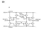
- the first to eighth transistors, the first and second capacitive elements, the first and second wirings, the first and second input terminals, and the first and second output terminals are provided. It is a semiconductor device that has. One of the source or drain of the first transistor is electrically connected to the first wiring, and the other of the source or drain of the first transistor is one of the source or drain of the second transistor, one terminal of the first capacitance element. , And the other of the source or drain of the second transistor is electrically connected to the second wiring.
- the gate of the first transistor includes the gate of the fourth transistor, one of the source or drain of the eighth transistor, one of the source or drain of the seventh transistor, one terminal of the second capacitive element, and the gate of the sixth transistor.
- the gate of the second transistor is the other terminal of the first capacitive element, one of the source or drain of the fourth transistor, one of the source or drain of the third transistor, the gate of the eighth transistor, and It is electrically connected to the gate of the fifth transistor.
- the other of the source or drain of the fourth transistor is electrically connected to the first wiring
- the other of the source or drain of the third transistor is electrically connected to the second wiring
- the gate of the third transistor is the third.
- Electrically connected to the 2 input terminal, the other of the source or drain of the 8th transistor is electrically connected to the 1st wiring, and the other of the source or drain of the 7th transistor is electrically connected to the 2nd wiring.
- the gate of the 7th transistor is electrically connected to the 1st input terminal.
- One of the source or drain of the fifth transistor is electrically connected to the first wiring, and the other of the source or drain of the fifth transistor is one of the source or drain of the sixth transistor, the other terminal of the second capacitive element.
- the second output terminal is electrically connected, and the other of the source or drain of the sixth transistor is electrically connected to the second wiring.
- the first to eighth transistors are n-channel type.
- the first to eighth transistors have a metal oxide in the channel forming region.
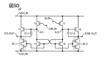
- one embodiment of the present invention includes first to sixth transistors, first and second capacitive elements, first and second wirings, first and second input terminals, and first and second output terminals. It is a semiconductor device having and. One of the source or drain of the first transistor is electrically connected to the first wiring, and the other of the source or drain of the first transistor is one of the source or drain of the second transistor, the gate of the fourth transistor, the first. It is electrically connected to one terminal of the capacitive element and the first output terminal, and the other of the source or drain of the second transistor is electrically connected to the second wiring.
- the gate of the first transistor is electrically connected to one of the source or drain of the fourth transistor, one of the source or drain of the fifth transistor, one terminal of the second capacitive element, and the second output terminal.
- the gate of the two transistors is electrically connected to one of the source or drain of the third transistor and the other terminal of the first capacitive element, and the gate of the third transistor is electrically connected to the second wiring.
- the other of the source or drain of the third transistor is electrically connected to the second input terminal.
- the other of the source or drain of the fourth transistor is electrically connected to the first wiring
- the other of the source or drain of the fifth transistor is electrically connected to the second wiring
- the gate of the fifth transistor is the third.
- the gate of the 6th transistor is electrically connected to the 2nd wiring and the source or drain of the 6th transistor.
- the other is electrically connected to the first input terminal.
- the first to sixth transistors are n-channel type.
- the first to sixth transistors have a metal oxide in the channel forming region.
- one embodiment of the present invention includes first to tenth transistors, first and second capacitive elements, first and second wirings, first to fourth input terminals, and first and second output terminals. It is a semiconductor device having and. One of the source or drain of the first transistor is electrically connected to the first wiring, and the other of the source or drain of the first transistor is one of the source or drain of the second transistor, one terminal of the first capacitance element. , And the other of the source or drain of the second transistor is electrically connected to the second wiring.
- the gate of the first transistor includes the gate of the fifth transistor, one of the source or drain of the tenth transistor, one of the source or drain of the ninth transistor, one terminal of the second capacitance element, and the gate of the seventh transistor.
- the gate of the second transistor is the other terminal of the first capacitive element, one of the source or drain of the fourth transistor, one of the source or drain of the third transistor, the source or drain of the fifth transistor.
- it is electrically connected to the gate of the 10th transistor and the gate of the 6th transistor.
- the other of the source or drain of the fifth transistor is electrically connected to the first wiring, and the other of the source or drain of the fourth transistor is electrically connected to the second wiring of the source or drain of the third transistor.
- the other is electrically connected to the second wiring, the gate of the fourth transistor is electrically connected to the fourth input terminal, and the gate of the third transistor is electrically connected to the second input terminal.
- the other of the source or drain of the tenth transistor is electrically connected to the first wiring
- the other of the source or drain of the ninth transistor is electrically connected to one of the source or drain of the eighth transistor
- the eighth The other of the transistor source or drain is electrically connected to the second wiring
- the gate of the ninth transistor is electrically connected to the third input terminal
- the gate of the eighth transistor is electrically connected to the first input terminal.
- One of the source or drain of the sixth transistor is electrically connected to the first wiring
- the other of the source or drain of the sixth transistor is one of the source or drain of the seventh transistor, the other terminal of the second capacitive element.
- the second output terminal is electrically connected, and the other of the source or drain of the seventh transistor is electrically connected to the second wiring.
- the first to tenth transistors are n-channel type.
- the first to tenth transistors have a metal oxide in the channel forming region.
- one embodiment of the present invention includes first to tenth transistors, first and second capacitive elements, first and second wirings, first to fourth input terminals, and first and second output terminals. It is a semiconductor device having and. One of the source or drain of the first transistor is electrically connected to the first wiring, and the other of the source or drain of the first transistor is one of the source or drain of the second transistor, one terminal of the first capacitance element. , And the other of the source or drain of the second transistor is electrically connected to the second wiring.
- the gate of the first transistor is the gate of the fifth transistor, one of the source or drain of the tenth transistor, one of the source or drain of the eighth transistor, one of the source or drain of the ninth transistor, and one of the second capacitive elements.
- the gate of the 2nd transistor is the other terminal of the 1st capacitive element, one of the source or drain of the 4th transistor, and the source or drain of the 5th transistor.
- it is electrically connected to the gate of the 10th transistor and the gate of the 6th transistor.
- the other of the source or drain of the fifth transistor is electrically connected to the first wiring
- the other of the source or drain of the fourth transistor is electrically connected to one of the source or drain of the third transistor
- the third The other of the transistor source or drain is electrically connected to the second wiring
- the gate of the fourth transistor is electrically connected to the fourth input terminal
- the gate of the third transistor is electrically connected to the second input terminal.
- the other of the source or drain of the tenth transistor is electrically connected to the first wiring
- the other of the source or drain of the eighth transistor is electrically connected to the second wiring of the source or drain of the ninth transistor.
- the other is electrically connected to the second wiring
- the gate of the eighth transistor is electrically connected to the first input terminal
- the gate of the ninth transistor is electrically connected to the third input terminal.
- One of the source or drain of the sixth transistor is electrically connected to the first wiring
- the other of the source or drain of the sixth transistor is one of the source or drain of the seventh transistor, the other terminal of the second capacitive element.
- the second output terminal is electrically connected, and the other of the source or drain of the seventh transistor is electrically connected to the second wiring.
- the first to tenth transistors are n-channel type.
- the first to tenth transistors have a metal oxide in the channel forming region.
- the first to eighth transistors, the first and second capacitive elements, the first and second wirings, the first and second input terminals, and the first and second output terminals are provided. It is a semiconductor device that has. One of the source or drain of the first transistor is electrically connected to the first wiring, and the other of the source or drain of the first transistor is one of the source or drain of the second transistor, one terminal of the first capacitance element. , And the other of the source or drain of the second transistor is electrically connected to the second wiring.
- the gate of the first transistor includes the gate of the fourth transistor, one of the source or drain of the eighth transistor, one of the source or drain of the seventh transistor, one terminal of the second capacitive element, and the gate of the sixth transistor.
- the gate of the second transistor is the other terminal of the first capacitive element, one of the source or drain of the fourth transistor, one of the source or drain of the third transistor, the gate of the eighth transistor, and It is electrically connected to the gate of the fifth transistor.
- the other of the source or drain of the fourth transistor is electrically connected to the first wiring
- the other of the source or drain of the third transistor is electrically connected to the second wiring
- the gate of the third transistor is the third.
- Electrically connected to the 2 input terminal, the other of the source or drain of the 8th transistor is electrically connected to the 1st wiring, and the other of the source or drain of the 7th transistor is electrically connected to the 2nd wiring.
- the gate of the 7th transistor is electrically connected to the 1st input terminal.
- One of the source or drain of the fifth transistor is electrically connected to the first wiring, and the other of the source or drain of the fifth transistor is one of the source or drain of the sixth transistor, the other terminal of the second capacitive element.
- the second output terminal is electrically connected, and the other of the source or drain of the sixth transistor is electrically connected to the second wiring.
- the first potential is supplied to the first wiring
- the second potential is supplied to the second wiring
- the second potential is a potential higher than the first potential
- the first signal is input to the first input terminal.
- the second signal is input to the second input terminal, and the second signal is a signal in which the logic of the first signal is inverted.
- the first to eighth transistors are n-channel type.
- the first to eighth transistors have a metal oxide in the channel forming region.
- one embodiment of the present invention includes first to sixth transistors, first and second capacitive elements, first and second wirings, first and second input terminals, and first and second output terminals. It is a semiconductor device having and. One of the source or drain of the first transistor is electrically connected to the first wiring, and the other of the source or drain of the first transistor is one of the source or drain of the second transistor, the gate of the fourth transistor, the first. It is electrically connected to one terminal of the capacitive element and the first output terminal, and the other of the source or drain of the second transistor is electrically connected to the second wiring.
- the gate of the first transistor is electrically connected to one of the source or drain of the fourth transistor, one of the source or drain of the fifth transistor, one terminal of the second capacitive element, and the second output terminal.
- the gate of the two transistors is electrically connected to one of the source or drain of the third transistor and the other terminal of the first capacitive element, and the gate of the third transistor is electrically connected to the second wiring.
- the other of the source or drain of the third transistor is electrically connected to the second input terminal.
- the other of the source or drain of the fourth transistor is electrically connected to the first wiring
- the other of the source or drain of the fifth transistor is electrically connected to the second wiring
- the gate of the fifth transistor is the third.
- the gate of the 6th transistor is electrically connected to the 2nd wiring and the source or drain of the 6th transistor.
- the other is electrically connected to the first input terminal.
- the first potential is supplied to the first wiring
- the second potential is supplied to the second wiring
- the second potential is a potential higher than the first potential
- the first signal is input to the first input terminal.
- the second signal is input to the second input terminal, and the second signal is a signal in which the logic of the first signal is inverted.
- the first to sixth transistors are n-channel type.
- the first to sixth transistors have a metal oxide in the channel forming region.
- one embodiment of the present invention includes first to tenth transistors, first and second capacitive elements, first and second wirings, first to fourth input terminals, and first and second output terminals. It is a semiconductor device having and. One of the source or drain of the first transistor is electrically connected to the first wiring, and the other of the source or drain of the first transistor is one of the source or drain of the second transistor, one terminal of the first capacitance element. , And the other of the source or drain of the second transistor is electrically connected to the second wiring.
- the gate of the first transistor includes the gate of the fifth transistor, one of the source or drain of the tenth transistor, one of the source or drain of the ninth transistor, one terminal of the second capacitance element, and the gate of the seventh transistor.
- the gate of the second transistor is the other terminal of the first capacitive element, one of the source or drain of the fourth transistor, one of the source or drain of the third transistor, the source or drain of the fifth transistor.
- it is electrically connected to the gate of the 10th transistor and the gate of the 6th transistor.
- the other of the source or drain of the fifth transistor is electrically connected to the first wiring, and the other of the source or drain of the fourth transistor is electrically connected to the second wiring of the source or drain of the third transistor.
- the other is electrically connected to the second wiring, the gate of the fourth transistor is electrically connected to the fourth input terminal, and the gate of the third transistor is electrically connected to the second input terminal.
- the other of the source or drain of the tenth transistor is electrically connected to the first wiring
- the other of the source or drain of the ninth transistor is electrically connected to one of the source or drain of the eighth transistor
- the eighth The other of the transistor source or drain is electrically connected to the second wiring
- the gate of the ninth transistor is electrically connected to the third input terminal
- the gate of the eighth transistor is electrically connected to the first input terminal.
- One of the source or drain of the sixth transistor is electrically connected to the first wiring
- the other of the source or drain of the sixth transistor is one of the source or drain of the seventh transistor, the other terminal of the second capacitive element.
- the second output terminal is electrically connected, and the other of the source or drain of the seventh transistor is electrically connected to the second wiring.
- a first potential is supplied to the first wiring
- a second potential is supplied to the second wiring
- the second potential is a potential higher than the first potential
- the first signal is input to the first input terminal.
- the second signal is input to the second input terminal
- the third signal is input to the third input terminal
- the fourth signal is input to the fourth input terminal
- the second signal is the logic of the first signal. Is an inverted signal
- the fourth signal is a signal in which the logic of the third signal is inverted.
- the first to tenth transistors are n-channel type.
- the first to tenth transistors have a metal oxide in the channel forming region.
- one embodiment of the present invention includes first to tenth transistors, first and second capacitive elements, first and second wirings, first to fourth input terminals, and first and second output terminals. It is a semiconductor device having and. One of the source or drain of the first transistor is electrically connected to the first wiring, and the other of the source or drain of the first transistor is one of the source or drain of the second transistor, one terminal of the first capacitance element. , And the other of the source or drain of the second transistor is electrically connected to the second wiring.
- the gate of the first transistor is the gate of the fifth transistor, one of the source or drain of the tenth transistor, one of the source or drain of the eighth transistor, one of the source or drain of the ninth transistor, and one of the second capacitive elements.
- the gate of the 2nd transistor is the other terminal of the 1st capacitive element, one of the source or drain of the 4th transistor, and the source or drain of the 5th transistor.
- it is electrically connected to the gate of the 10th transistor and the gate of the 6th transistor.
- the other of the source or drain of the fifth transistor is electrically connected to the first wiring
- the other of the source or drain of the fourth transistor is electrically connected to one of the source or drain of the third transistor
- the third The other of the transistor source or drain is electrically connected to the second wiring
- the gate of the fourth transistor is electrically connected to the fourth input terminal
- the gate of the third transistor is electrically connected to the second input terminal.
- the other of the source or drain of the tenth transistor is electrically connected to the first wiring
- the other of the source or drain of the eighth transistor is electrically connected to the second wiring of the source or drain of the ninth transistor.
- the other is electrically connected to the second wiring
- the gate of the eighth transistor is electrically connected to the first input terminal
- the gate of the ninth transistor is electrically connected to the third input terminal.
- One of the source or drain of the sixth transistor is electrically connected to the first wiring
- the other of the source or drain of the sixth transistor is one of the source or drain of the seventh transistor, the other terminal of the second capacitive element.
- the second output terminal is electrically connected, and the other of the source or drain of the seventh transistor is electrically connected to the second wiring.
- a first potential is supplied to the first wiring
- a second potential is supplied to the second wiring
- the second potential is a potential higher than the first potential
- the first signal is input to the first input terminal.
- the second signal is input to the second input terminal
- the third signal is input to the third input terminal
- the fourth signal is input to the fourth input terminal
- the second signal is the logic of the first signal. Is an inverted signal
- the fourth signal is a signal in which the logic of the third signal is inverted.
- the first to tenth transistors are n-channel type.
- the first to tenth transistors have a metal oxide in the channel forming region.
- the logic circuit is configured by using a unipolar transistor, when the steady current does not flow and the output is high level, the potential of the output terminal rises to the high power supply potential and the output is low level. At this time, it is possible to provide a logic circuit in which the potential of the output terminal drops to a low power supply potential.
- the semiconductor device is configured by using a unipolar transistor, when the steady current does not flow and the output is at a high level, the potential of the output terminal rises to a high power supply potential and the output becomes high. It is possible to provide a semiconductor device in which the potential of the output terminal drops to a low power supply potential at a low level.
- FIG. 1 is a circuit diagram showing a configuration example of a semiconductor device.
- FIG. 2 is a timing chart.
- FIG. 3 is a circuit diagram showing a configuration example of a semiconductor device.
- FIG. 4 is a timing chart.
- 5A and 5B are diagrams showing circuit diagram symbols of transistors.
- 5C and 5D are circuit diagrams showing a configuration example of a semiconductor device.
- FIG. 6 is a circuit diagram showing a configuration example of a semiconductor device.
- FIG. 7 is a circuit diagram showing a configuration example of a semiconductor device.
- FIG. 8 is a timing chart.
- FIG. 9 is a cross-sectional view showing a configuration example of the semiconductor device.
- 10A, 10B, and 10C are cross-sectional views showing a structural example of the transistor.
- FIG. 11A is a top view showing a structural example of the transistor.
- 11B and 11C are cross-sectional views showing a structural example of the transistor.
- FIG. 12A is a top view showing a structural example of the transistor.
- 12B and 12C are cross-sectional views showing a structural example of the transistor.
- FIG. 13A is a top view showing a structural example of the transistor.
- 13B and 13C are cross-sectional views showing a structural example of the transistor.
- FIG. 14A is a top view showing a structural example of the transistor.
- 14B and 14C are cross-sectional views showing a structural example of the transistor.
- FIG. 15A is a top view showing a structural example of the transistor.
- 15B and 15C are cross-sectional views showing a structural example of the transistor.
- FIG. 15A is a top view showing a structural example of the transistor.
- 15B and 15C are cross-sectional views showing a structural example of the transistor.
- 16A is a top view showing a structural example of the transistor.
- 16B and 16C are cross-sectional views showing a structural example of the transistor.
- 17A and 17B are cross-sectional views showing a structural example of the transistor.
- FIG. 18 is a cross-sectional view showing a configuration example of the semiconductor device.
- 19A and 19B are cross-sectional views showing a structural example of the transistor.
- FIG. 20A is a diagram illustrating classification of the crystal structure of IGZO.
- FIG. 20B is a diagram illustrating an XRD spectrum of quartz glass.
- FIG. 20C is a diagram illustrating an XRD spectrum of crystalline IGZO.
- FIG. 20D is a diagram illustrating a microelectron diffraction pattern of crystalline IGZO.
- membrane and the term “layer” can be interchanged with each other.
- conductive layer to the term “conductive layer”.
- insulating film to the term “insulating layer”.
- gate electrode on the gate insulating layer does not exclude those containing other components between the gate insulating layer and the gate electrode.
- the code when the same code is used for a plurality of elements, and when it is particularly necessary to distinguish them, the code may be "_1", “_2", “[n]", “[m,”. It may be described with an identification code such as "n]".
- the second wiring GL is described as wiring GL [2].
- “electrically connected” includes a case where they are connected via "something having some kind of electrical action".
- the "thing having some kind of electrical action” is not particularly limited as long as it enables the exchange of electric signals between the connection targets.
- “things having some kind of electrical action” include electrodes, wirings, switching elements such as transistors, resistance elements, inductors, capacitive elements, and other elements having various functions. Further, even when it is expressed as “electrically connected”, there is a case where there is no physical connection part in the actual circuit and only the wiring is extended.
- Electrode and “wiring” do not functionally limit these components.
- an “electrode” may be used as part of a “wiring” and vice versa.
- the "terminal" in the electric circuit means a portion where current or potential input (or output) and signal reception (or transmission) are performed. Therefore, a part of the wiring or the electrode may function as a terminal.
- the “capacity” has a configuration in which two electrodes face each other via an insulator (dielectric).
- the “capacitive element” includes the above-mentioned “capacity”. That is, in the present specification and the like, the “capacitive element” has a structure in which two electrodes face each other via an insulator, a structure in which two wires face each other via an insulator, or a structure in which two wires face each other through an insulator. This includes the case where the two wires are arranged via an insulator.
- the “voltage” often indicates a potential difference between a certain potential and a reference potential (for example, a ground potential). Therefore, the voltage and the potential difference can be rephrased.
- a transistor is an element having at least three terminals including a gate, a drain, and a source. Then, a channel forming region is provided between the drain (drain terminal, drain region, or drain electrode) and the source (source terminal, source region, or source electrode), and the source and drain are passed through the channel forming region. It is possible to pass a current between and.
- the channel forming region means a region in which a current mainly flows.
- the functions of the source and the drain may be interchanged when transistors having different polarities are adopted or when the direction of the current changes in the circuit operation. Therefore, in the present specification and the like, the terms source and drain can be used interchangeably.
- the off current means a drain current when the transistor is in an off state (also referred to as a non-conducting state or a cutoff state).
- the off state means that the gate voltage Vgs with respect to the source is lower than the threshold voltage Vth in the n-channel transistor, and the gate voltage Vgs with respect to the source is the threshold voltage in the p-channel transistor.
- drain may be read as source. That is, the off current may refer to the source current when the transistor is in the off state. In addition, it may be called a leak current in the same meaning as an off current. Further, in the present specification and the like, the off current may refer to the current flowing between the source and the drain when the transistor is in the off state.
- the on-current may refer to the current flowing between the source and the drain when the transistor is in the on state (also referred to as the conduction state).
- a metal oxide is a metal oxide in a broad sense. Metal oxides are classified into oxide insulators, oxide conductors (including transparent oxide conductors), oxide semiconductors, and the like.
- the metal oxide when a metal oxide is used in the channel forming region of a transistor, the metal oxide may be referred to as an oxide semiconductor. That is, when a metal oxide has at least one of an amplification action, a rectifying action, and a switching action, the metal oxide can be referred to as a metal oxide semiconductor (metal oxide semiconductor). That is, a transistor having a metal oxide in the channel forming region can be called an "oxide semiconductor transistor" or an "OS transistor". Similarly, the above-mentioned "transistor using an oxide semiconductor” is also a transistor having a metal oxide in the channel forming region.
- a metal oxide having nitrogen may also be referred to as a metal oxide. Further, a metal oxide having nitrogen may be referred to as a metal oxynitride. Details of the metal oxide will be described later.
- the semiconductor device according to one embodiment of the present invention is a logic circuit configured by using a unipolar transistor, in which a high power supply potential is used to represent a high level, and a low power supply potential is used to represent a low level.
- n-channel type transistor is used for the semiconductor device described in the present specification and the like
- p-channel type transistor can also be used.
- the change from the n-channel transistor to the p-channel transistor is easily understood by those skilled in the art, and the description thereof will be omitted.
- FIG. 1 is a circuit diagram showing a configuration example of the semiconductor device 10.
- the semiconductor device 10 is a semiconductor device according to an embodiment of the present invention, and includes transistors 11 to 18, a capacitive element C11, and a capacitive element C12.
- the transistor 11 to 18 is an n-channel type transistor.
- the semiconductor device 10 provides wiring VSS_IN to which the low power potential VSS is supplied, wiring VDD_IN to which the high power potential VDD is supplied, input terminal SI_IN to which the signal SI is input, input terminal SIB_IN to which the signal SIB is input, and signal SO. It has an output terminal SO_OUT for output and an output terminal SOB_OUT for outputting a signal SOB.
- the high power supply potential VDD is a potential higher than the low power supply potential VSS
- the low power supply potential VSS may be used as a reference potential in the semiconductor device 10.
- the signal SI and the signal SIB are digital signals, the potential representing the high level of the signal SI and the signal SIB can be the high power supply potential VDD, and the potential representing the low level can be the low power supply potential VSS. ..
- the signal SIB is a signal in which the logic of the signal SI is inverted.
- one of the source or drain of the transistor 11 is electrically connected to the wiring VSS_IN
- the other of the source or drain of the transistor 11 is one of the source or drain of the transistor 12, and one terminal of the capacitive element C11.
- the output terminal SO_OUT, and the other of the source or drain of the transistor 12 is electrically connected to the wiring VDD_IN.
- the gate of the transistor 11 is electrically connected to the gate of the transistor 14, one of the source or drain of the transistor 18, one of the source or drain of the transistor 17, one terminal of the capacitive element C12, and the gate of the transistor 16. .. Further, the gate of the transistor 12 is electrically connected to the other terminal of the capacitive element C11, one of the source or drain of the transistor 14, one of the source or drain of the transistor 13, the gate of the transistor 18, and the gate of the transistor 15. Will be done.
- the other of the source or drain of the transistor 14 is electrically connected to the wiring VSS_IN
- the other of the source or drain of the transistor 13 is electrically connected to the wiring VDD_IN
- the gate of the transistor 13 is electrically connected to the input terminal SIB_IN.
- the other of the source or drain of the transistor 18 is electrically connected to the wiring VSS_IN
- the other of the source or drain of the transistor 17 is electrically connected to the wiring VDD_IN
- the gate of the transistor 17 is connected to the input terminal SI_IN. It is electrically connected.
- One of the source or drain of the transistor 15 is electrically connected to the wiring VSS_IN, and the other of the source or drain of the transistor 15 is one of the source or drain of the transistor 16, the other terminal of the capacitive element C12, and the output terminal. It is electrically connected to SOB_OUT and the other of the source or drain of transistor 16 is electrically connected to wiring VDD_IN.
- connection between the gate of the transistor 11 and the gate of the transistor 14, one of the source or drain of the transistor 18, one of the source or drain of the transistor 17, one terminal of the capacitive element C12, and the gate of the transistor 16. Is referred to as node N12.
- connection between the gate of the transistor 12 and the other terminal of the capacitive element C11, one of the source or drain of the transistor 14, one of the source or drain of the transistor 13, the gate of the transistor 18, and the gate of the transistor 15 Called node N11.
- FIG. 2 is a timing chart showing an operation example of the semiconductor device 10.
- FIG. 2 shows the potentials of the signal SI, the signal SIB, the node N11, the node N12, the signal SO, and the signal SOB by dividing them into periods D11 to D14. It is assumed that the threshold voltage of the transistors 11 to 18 is the threshold voltage Vth.
- the period D11 is a period in which the signal SI is at a high level and the signal SIB is at a low level.
- a static state is considered as the initial state. Since the signal SI is at a high level, the transistor 17 is in a conductive state and the node N12 is at a high level. However, the potential of the node N12 in this period is lower than the high power supply potential VDD, and is a value obtained by subtracting the threshold voltage Vth from the high power supply potential VDD. Further, since the signal SIB is at a low level, the transistor 13 is in a non-conducting state.
- the transistor 14, the transistor 11, and the transistor 16 are in a conductive state, and the node N11 is at a low level. Further, the transistor 18, the transistor 15, and the transistor 12 are in a non-conducting state.
- the signal SO is at a low level. Further, since the transistor 16 is in the conductive state and the transistor 15 is in the non-conducting state, the signal SOB is at a high level. However, the potential of the signal SOB during this period is lower than the high power supply potential VDD, similar to the node N12.
- the period D12 is a period in which the signal SI changes from high level to low level and the signal SIB changes from low level to high level (the period in which the signal changes from high level to low level is the falling period, and the period from low level to high level).
- the period during which the signal SI changes to is also referred to as the rise period), and the signal SI is at the low level and the signal SIB is at the high level.
- the transistor 17 changes from the conductive state to the non-conducting state, and the transistor 13 changes from the non-conducting state to the conducting state.
- the node N11 becomes a high level.
- the transistor 18 changes to the conductive state, and the node N12 becomes the low level.
- the transistor 18, the transistor 15, and the transistor 12 become conductive. Further, when the node N12 becomes low level, the transistor 14, the transistor 11, and the transistor 16 are in a non-conducting state.
- the signal SO becomes a high level. Further, since the transistor 16 is in the non-conducting state and the transistor 15 is in the conducting state, the signal SOB is at a low level.
- the time from when the node N11 reaches the high level until the node N12 reaches the low level is defined as the delay time DT12. Even if the node N11 becomes high level and the transistor 12 becomes conductive, the transistor 11 remains conductive until the node N12 becomes low level. Therefore, the signal SO reaches the high level later than the timing when the node N11 becomes the high level.
- the potential difference DV12 is also applied between one terminal of the capacitance element C11 and the other terminal of the capacitance element C11.
- the signal SO changes from a low level to a high level, the potential of the node N11 rises due to the capacitive coupling by the capacitive element C11, and the potential of the node N11 can be made higher than the high power supply potential VDD.
- the potential of the signal SO can be set to the high power supply potential VDD. Further, the potential of the node N11 higher than the high power supply potential VDD is obtained during the period when the signal SI is at a low level (when the signal SIB is at a high level) by using a transistor having a small off current, which will be described later, for the transistor 13 and the transistor 14. It can be retained even if it is long (for a certain period).
- the period D13 is a period in which the signal SI changes from low level to high level and the signal SIB changes from high level to low level, and a period in which the signal SI is high level and the signal SIB is low level.
- the transistor 17 changes from the non-conducting state to the conducting state, and the transistor 13 changes from the conducting state to the non-conducting state.
- the node N12 becomes a high level.
- the transistor 14 changes to a conductive state and the node N11 goes low.
- the transistor 14 When the node N12 reaches a high level, the transistor 14, the transistor 11, and the transistor 16 become conductive. Further, when the node N11 becomes low level, the transistor 18, the transistor 15, and the transistor 12 are in a non-conducting state.
- the signal SO is at a low level. Further, since the transistor 16 is in the conductive state and the transistor 15 is in the non-conducting state, the signal SOB becomes a high level.
- the time from when the node N12 becomes the high level until the node N11 becomes the low level is defined as the delay time DT13. Even if the node N12 becomes high level and the transistor 16 becomes conductive, the transistor 15 remains conductive until the node N11 becomes low level. Therefore, the signal SOB reaches the high level later than the timing when the node N12 becomes the high level.
- the signal SOB becomes high level after the timing when the node N12 becomes high level, a potential difference is generated between the output terminal SOB_OUT and the node N12. Assuming that the potential difference is the potential difference DV13, the potential difference DV13 is also applied between one terminal of the capacitance element C12 and the other terminal of the capacitance element C12.
- the signal SOB changes from a low level to a high level, the potential of the node N12 rises due to the capacitive coupling by the capacitive element C12, and the potential of the node N12 can be made higher than the high power supply potential VDD.
- the potential of the signal SOB can be set to the high power supply potential VDD. Further, the potential of the node N12, which is higher than the high power supply potential VDD, is the period during which the signal SI is at a high level (the signal SIB is at a low level) by using a transistor having a small off current, which will be described later, for the transistor 17 and the transistor 18. It can be retained even if it is long (for a certain period).
- the period D14 is a period in which the signal SI changes from high level to low level and the signal SIB changes from low level to high level, and a period in which the signal SI is low level and the signal SIB is high level. Since the period D14 is the same as the period D12, the description thereof will be omitted.
- the semiconductor device 10 is a logic circuit configured by using an n-channel transistor, and by securing a potential difference DV12 between the output terminal SO_OUT and the node N11 by the delay time DT12, Patent Document 1
- the potential of the node N11 can be made higher than the high power supply potential VDD more reliably than the example disclosed in Patent Document 2.
- the potential of the node N12 can be more reliably set to the higher power supply potential than the example disclosed in Patent Document 1 or Patent Document 2. It can be higher than VDD.
- the potential of the node N11 rises to a high power supply potential VDD by making the potential higher than the high power supply potential VDD.
- the signal SOB output from the output terminal SOB_OUT is at a high level
- the potential of the node N12 rises to a high power supply potential VDD by making the potential higher than the high power supply potential VDD.
- the signal SO and the signal SOB decrease to the low power potential VSS at the low level, and after the high level or the low level of the signal SO and the signal SOB is determined in the semiconductor device 10, the high power potential VDD is low. It has the characteristic that no through current flows through the power supply potential VSS.
- FIG. 3 is a circuit diagram showing a configuration example of the semiconductor device 20.
- the semiconductor device 20 is a semiconductor device according to an embodiment of the present invention, and is a configuration example different from the semiconductor device 10.
- the semiconductor device 20 includes transistors 21 to 26, a capacitive element C21, and a capacitive element C22.
- the transistor 21 to the transistor 26 are n-channel type transistors.
- the semiconductor device 20 has a wiring VSS_IN to which a low power supply potential VSS is supplied, a wiring VDD_IN to which a high power supply potential VDD is supplied, an input terminal SI_IN to which a signal SI is input, and an input to which a signal SIB is input. It has a terminal SIB_IN, an output terminal SO_OUT that outputs a signal SO, and an output terminal SOB_OUT that outputs a signal SOB. Since the description will be repeated, the description of the potential and the signal will be omitted.
- one of the source or drain of the transistor 21 is electrically connected to the wiring VSS_IN, and the other of the source or drain of the transistor 21 is one of the source or drain of the transistor 22, the gate of the transistor 24, and the capacitive element. It is electrically connected to one terminal of C21 and the output terminal SO_OUT, and the other of the source or drain of the transistor 22 is electrically connected to the wiring VDD_IN.
- the gate of the transistor 21 is electrically connected to one of the source or drain of the transistor 24, one of the source or drain of the transistor 25, one terminal of the capacitive element C22, and the output terminal SOB_OUT, and the gate of the transistor 22 is connected to the gate of the transistor 22. It is electrically connected to one of the source or drain of the transistor 23 and the other terminal of the capacitive element C21. Further, the gate of the transistor 23 is electrically connected to the wiring VDD_IN, and the other of the source or drain of the transistor 23 is electrically connected to the input terminal SIB_IN.
- the other of the source or drain of the transistor 24 is electrically connected to the wiring VSS_IN
- the other of the source or drain of the transistor 25 is electrically connected to the wiring VDD_IN
- the gate of the transistor 25 is the source or drain of the transistor 26. It is electrically connected to one terminal and the other terminal of the capacitive element C22. Further, the gate of the transistor 26 is electrically connected to the wiring VDD_IN, and the other of the source or drain of the transistor 26 is electrically connected to the input terminal SI_IN.
- connection portion between the gate of the transistor 22 and one of the source or drain of the transistor 23 and the other terminal of the capacitive element C21 is referred to as a node N21
- the connection portion between one of the drains and the other terminal of the capacitance element C22 is referred to as a node N22.
- FIG. 4 is a timing chart showing an operation example of the semiconductor device 20.
- FIG. 4 shows the potentials of the signal SI, the signal SIB, the node N21, the node N22, the signal SO, and the signal SOB by dividing them into periods D21 to D24. It is assumed that the threshold voltage of the transistors 21 to 26 is the threshold voltage Vth.
- the period D21 is a period in which the signal SI is at a high level and the signal SIB is at a low level.
- a static state is considered as the initial state.
- the transistor 26 is in a conductive state, and the potential of the node N22 is at a high level like the signal SI. Further, the transistor 23 is in a conductive state, and the potential of the node N21 is at a low level like the signal SIB.
- the potential of the node N22 in this period is lower than the high power supply potential VDD, and is a value obtained by subtracting the threshold voltage Vth from the high power supply potential VDD.
- the transistor 25 Since the node N22 is at a high level, the transistor 25 is in a conductive state and the signal SOB is at a high level. However, the potential of the signal SOB during this period is lower than the high power supply potential VDD, similar to the node N22. Further, the transistor 21 is in a conductive state.
- the transistor 22 Since the node N21 is at a low level, the transistor 22 is in a non-conducting state. Further, since the transistor 21 is in a conductive state, the signal SO is at a low level. Further, the transistor 24 is in a non-conducting state.
- the period D22 is a period in which the signal SI changes from high level to low level and the signal SIB changes from low level to high level, and a period in which the signal SI is low level and the signal SIB is high level.
- node N22 changes from high level to low level and transistor 25 changes from conductive to non-conductive. Further, the node N21 changes from a low level to a high level, and the transistor 22 changes from a non-conducting state to a conducting state.
- the signal SO becomes high level.
- the signal SOB does not immediately reach the low level.
- the transistor 24 changes to the conductive state, and the signal SOB becomes low level. Further, when the signal SOB becomes low level, the transistor 21 is in a non-conducting state.
- the transistor 21 is in a conductive state until the signal SOB becomes a low level. Therefore, the potential of the signal SO is lower than the high power supply potential VDD, and the potential of the signal SO rises again after the transistor 21 becomes non-conducting.
- the potential difference DV22 is also applied between one terminal of the capacitance element C21 and the other terminal of the capacitance element C21, when the signal SO changes from a low level to a high level, the capacitance coupling by the capacitance element C21 causes the potential difference DV22.
- the potential of the node N21 can be made higher than the high power supply potential VDD.
- the potential of the signal SO can be set to the high power supply potential VDD. Further, the potential of the node N21 higher than the high power supply potential VDD is the period during which the signal SI is at a low level (the period during which the signal SIB is at a high level) by using a transistor having a small off current, which will be described later, for the transistor 23. Can be retained even if it is long.
- the period D23 is a period in which the signal SI changes from low level to high level and the signal SIB changes from high level to low level, and a period in which the signal SI is high level and the signal SIB is low level.
- the node N21 changes from high level to low level and the transistor 22 changes from a conductive state to a non-conducting state. Further, the node N22 changes from a low level to a high level, and the transistor 25 changes from a non-conducting state to a conducting state.
- the signal SOB becomes high level.
- the signal SO does not immediately reach the low level.
- the transistor 21 changes to a conductive state and the signal SO goes low. Further, when the signal SO becomes low level, the transistor 24 is in a non-conducting state.
- the transistor 24 is in a conductive state until the signal SO becomes a low level. Therefore, the potential of the signal SOB is lower than the high power supply potential VDD, and the potential of the signal SOB rises again after the transistor 24 is in the non-conducting state.
- the potential difference DV23 is also applied between one terminal of the capacitance element C22 and the other terminal of the capacitance element C22, when the signal SOB changes from a low level to a high level, the capacitance coupling by the capacitance element C22 causes the potential difference DV23.
- the potential of the node N22 can be made higher than the high power supply potential VDD.
- the potential of the signal SOB can be set to the high power supply potential VDD. Further, the potential of the node N22, which is higher than the high power supply potential VDD, is the period during which the signal SI is at a high level (the period during which the signal SIB is at a low level) by using a transistor having a small off current, which will be described later, for the transistor 26. Can be retained even if it is long.
- the period D24 is a period in which the signal SI changes from high level to low level and the signal SIB changes from low level to high level, and a period in which the signal SI is low level and the signal SIB is high level. Since the period D24 is the same as the period D22, the description thereof will be omitted.
- the semiconductor device 20 is a logic circuit configured by using an n-channel transistor, and when a potential difference DV22 is generated between the output terminal SO_OUT and the node N21, Patent Document 1 or Patent Document 2
- the potential of the node N21 can be made higher than the high power supply potential VDD more reliably than the example disclosed in.
- the potential difference DV23 is generated between the output terminal SOB_OUT and the node N22, so that the potential of the node N22 is surely higher than the high power supply potential VDD as compared with the example disclosed in Patent Document 1 or Patent Document 2. be able to.
- the potential of the node N21 rises to a high power supply potential VDD by making the potential higher than the high power supply potential VDD.
- the signal SOB output from the output terminal SOB_OUT is at a high level
- the potential of the node N22 rises to a high power supply potential VDD by making the potential higher than the high power supply potential VDD.
- the signal SO and the signal SOB decrease to the low power potential VSS at the low level, and after the high level or the low level of the signal SO and the signal SOB is determined in the semiconductor device 20, the high power potential VDD is low. It has the characteristic that no through current flows through the power supply potential VSS.
- Transistors that make up semiconductor devices Transistors (OS transistors) having a metal oxide in the channel forming region can be used for the transistors 11 to 18 constituting the semiconductor device 10 and the transistors 21 to 26 constituting the semiconductor device 20.
- the OS transistor has features such as a very small off-current, a high voltage can be applied between the source and the drain, and the thin film transistor can be provided in a stacked manner.
- the off current is the drain current when the transistor is in the off state, and the band gap of the oxide semiconductor is 2.5 eV or more, preferably 3.0 eV or more, so that the OS transistor is thermally excited. It has the characteristics that the leakage current is small and the off current is very small.
- the OS transistor can have, for example, an off-current per channel width of 1 ⁇ m of 100 zA / ⁇ m or less, or 10 zA / ⁇ m or less, or 1 zA / ⁇ m or less, or 10 yA / ⁇ m or less.
- the transistor 13 it is preferable to use a transistor having a small off current for the transistor 13, the transistor 14, the transistor 17, the transistor 18, the transistor 23, and the transistor 26.
- the period D12 or the period D22 even if the period during which the signal SI is at a low level (the period during which the signal SIB is at a high level) is long, the potential of the node N11 or the node N21 that has risen beyond the high power supply potential VDD can be increased. , Can be held for a long time.
- the potential of the node N12 or the node N22 that has risen beyond the high power supply potential VDD is applied for a long time. Can be retained.
- the OS transistor is characterized in that the off-current does not easily increase even in a high-temperature environment, and the ratio of the on-current to the off-current is large even in a high-temperature environment.
- the metal oxide used in the channel forming region of the OS transistor is preferably an oxide semiconductor containing at least one of indium (In) and zinc (Zn).
- an oxide semiconductor In—M—Zn oxide (element M is, for example, Al, Ga, Y or Sn) is typical.
- the oxide semiconductor can be made i-type (intrinsic) or substantially i-type.
- Such an oxide semiconductor can be called a highly purified oxide semiconductor.
- the OS transistor is a thin film transistor, it can be provided in a laminated manner.
- an OS transistor can be provided on a circuit configured by using a Si transistor formed on a single crystal silicon substrate. Therefore, the chip area of the semiconductor device 10 or the semiconductor device 20 can be reduced.
- transistors other than OS transistors may be used for the transistors 11 to 18 constituting the semiconductor device 10 and the transistors 21 to 26 constituting the semiconductor device 20.
- a transistor having a semiconductor having a large bandgap in the channel formation region may be used.
- the semiconductor having a large bandgap may refer to a semiconductor having a bandgap of 2.2 eV or more, and examples thereof include silicon carbide, gallium nitride, and diamond.
- a transistor having a back gate may be used for the transistors 11 to 18 constituting the semiconductor device 10 and the transistors 21 to 26 constituting the semiconductor device 20.
- FIG. 5A shows a circuit diagram symbol of the transistor 31.
- the transistor 31 has four terminals called a gate (also referred to as a front gate), a drain, a source, and a back gate.
- a gate also referred to as a front gate
- a drain also referred to as a drain
- a source also referred to as a source
- a back gate In FIG. 5A, they are represented as G (gate), D (drain), S (source), and BG (back gate), respectively.
- the back gate is electrically connected to the gate, the back gate is electrically connected to the source, a predetermined potential is applied to the back gate, or the back gate is electrically suspended (floating). It may be said).
- the back gate is electrically connected to the gate, the on-current of the transistor 31 can be increased.
- the threshold voltage of the transistor 31 can be changed by applying a predetermined potential to the back gate.
- a transistor having a plurality of gates may be used for the transistors 11 to 18 constituting the semiconductor device 10 and the transistors 21 to 26 constituting the semiconductor device 20.
- FIG. 5B shows a circuit diagram symbol of the transistor 32 having two gates (also referred to as a double gate).
- the transistor 32 has four terminals (gate 1, gate 2, drain, source). In FIG. 5B, they are represented as G1 (gate 1), G2 (gate 2), D (drain), and S (source), respectively.
- the gate 1 and the gate 2 may be electrically connected, or a predetermined potential may be applied to the gate 1 or the gate 2.
- a predetermined potential may be applied to the gate 1 or the gate 2.
- the off-current of the transistor 32 may be reduced by electrically connecting the gate 1 and the gate 2.
- the transistor 32 may be made into a transistor having a high withstand voltage.
- FIG. 5C an example in which a transistor 31 having a back gate is used for the transistor 11 and the transistor 15 constituting the semiconductor device 10 is shown in FIG. 5C (in FIG. 5C, the transistor 31_1 and the transistor 31_2 are shown, respectively).
- the back gate of the transistor 31 is electrically connected to the gate of the transistor 31.
- FIG. 5D an example in which a transistor 32 having two gates is used for the transistor 11 and the transistor 15 constituting the semiconductor device 10 is shown in FIG. 5D (in FIG. 5D, the transistor 32_1 and the transistor 32_2 are shown, respectively).
- the gate 1 of the transistor 32 is electrically connected to the gate 2 of the transistor 32.
- Embodiment 2 In this embodiment, an example of forming a general-purpose logic circuit by applying the semiconductor device 10 described in the above embodiment will be described.
- the semiconductor device 10 described in the above embodiment can be used as a NOT circuit that inverts the logic or a buffer circuit that does not invert the logic.
- the semiconductor device 10 receives a signal SI and a signal SIB, and outputs a signal SO and a signal SOB. Since the signal SIB is a signal in which the logic of the signal SI is inverted and the signal SOB is a signal in which the logic of the signal SO is inverted, the output terminal of the semiconductor device 10 is electrically connected to the input terminal of another semiconductor device 10. It is possible to connect to.
- FIG. 6 is a circuit diagram showing a configuration example of the semiconductor device 40.
- the semiconductor device 40 is a semiconductor device to which the semiconductor device 10 is applied, and has a function as a NAND circuit.
- the semiconductor device 40 includes transistors 41 to 50, a capacitive element C41, and a capacitive element C42.
- the transistor 41 to the transistor 50 are n-channel type transistors.
- the wiring VSS_IN to which the low power potential VSS is supplied, the wiring VDD_IN to which the high power potential VDD is supplied, the input terminal SI1_IN to which the signal SI1 is input, the input terminal SI2_IN to which the signal SI2 is input, and the signal SI1B are It has an input input terminal SI1B_IN, an input terminal SI2B_IN into which a signal SI2B is input, an output terminal SO1_OUT for outputting a signal SO1, and an output terminal SO1B_OUT for outputting a signal SO1B.
- the high power supply potential VDD is a potential higher than the low power supply potential VSS
- the low power supply potential VSS may be used as a reference potential in the semiconductor device 40.
- the signal SI1, the signal SI2, the signal SI1B, and the signal SI2B are digital signals, and the potential representing the high level of the signal SI1, the signal SI2, the signal SI1B, and the signal SI2B can be a high power supply potential VDD.
- the potential representing the low level can be a low power supply potential VSS.
- the signal SI1B is a signal in which the logic of the signal SI1 is inverted
- the signal SI2B is a signal in which the logic of the signal SI2 is inverted.
- one of the source or drain of the transistor 41 is electrically connected to the wiring VSS_IN, and the other of the source or drain of the transistor 41 is one of the source or drain of the transistor 42 and one terminal of the capacitive element C41.
- the output terminal SO1_OUT, and the other of the source or drain of the transistor 42 is electrically connected to the wiring VDD_IN.
- the gate of the transistor 41 is electrically connected to the gate of the transistor 45, one of the source or drain of the transistor 50, one of the source or drain of the transistor 49, one terminal of the capacitive element C42, and the gate of the transistor 47. Further, the gate of the transistor 42 is the other terminal of the capacitive element C41, one of the source or drain of the transistor 44, one of the source or drain of the transistor 43, one of the source or drain of the transistor 45, the gate of the transistor 50, and It is electrically connected to the gate of the transistor 46.
- the other of the source or drain of the transistor 45 is electrically connected to the wiring VSS_IN
- the other of the source or drain of the transistor 44 is electrically connected to the wiring VDD_IN
- the other of the source or drain of the transistor 43 is the wiring VDD_IN.
- the gate of the transistor 44 is electrically connected to the input terminal SI2B_IN
- the gate of the transistor 43 is electrically connected to the input terminal SI1B_IN.
- the other of the source or drain of transistor 50 is electrically connected to the wiring VSS_IN
- the other of the source or drain of transistor 49 is electrically connected to one of the source or drain of transistor 48
- the source or drain of transistor 48 is electrically connected to the input terminal SI1_IN.
- One of the source or drain of the transistor 46 is electrically connected to the wiring VSS_IN, and the other of the source or drain of the transistor 46 is one of the source or drain of the transistor 47, the other terminal of the capacitive element C42, and the output terminal. It is electrically connected to SO1B_OUT and the other of the source or drain of the transistor 47 is electrically connected to the wiring VDD_IN.
- connection between the gate of the transistor 41 and the gate of the transistor 45, one of the source or drain of the transistor 50, one of the source or drain of the transistor 49, one terminal of the capacitive element C42, and the gate of the transistor 47. Is referred to as a node N42.
- the gate of the transistor 42 and the other terminal of the capacitive element C41, one of the source or drain of the transistor 45, one of the source or drain of the transistor 44, one of the source or drain of the transistor 43, the gate of the transistor 50, and The connection portion of the transistor 46 with the gate is referred to as a node N41.
- An operation example of the semiconductor device 40 will be described later.
- FIG. 7 is a circuit diagram showing a configuration example of the semiconductor device 60.
- the semiconductor device 60 is a semiconductor device to which the semiconductor device 10 is applied, and has a function as a NOR circuit.
- the semiconductor device 60 includes transistors 61 to 70, a capacitive element C61, and a capacitive element C62.
- the transistor 61 to the transistor 70 are n-channel type transistors.
- the semiconductor device 60 has a wiring VSS_IN to which a low power supply potential VSS is supplied, a wiring VDD_IN to which a high power supply potential VDD is supplied, an input terminal SI1_IN to which a signal SI1 is input, and an input to which a signal SI2 is input. It has a terminal SI2_IN, an input terminal SI1B_IN to which the signal SI1B is input, an input terminal SI2B_IN to which the signal SI2B is input, an output terminal SO2_OUT to output the signal SO2, and an output terminal SO2B_OUT to output the signal SO2B. Since the description will be repeated, the description of the potential and the signal will be omitted.
- one of the source or drain of the transistor 61 is electrically connected to the wiring VSS_IN
- the other of the source or drain of the transistor 61 is one of the source or drain of the transistor 62
- one terminal of the capacitive element C61 is one of the input terminal of the transistor 62
- the output terminal SO2_OUT, and the other of the source or drain of the transistor 62 is electrically connected to the wiring VDD_IN.
- the gate of the transistor 61 is the gate of the transistor 65, one of the source or drain of the transistor 70, one of the source or drain of the transistor 68, one of the source or drain of the transistor 69, one terminal of the capacitive element C62, and the transistor 67. It is electrically connected to the gate of. Further, the gate of the transistor 62 is electrically connected to the other terminal of the capacitive element C61, one of the source or drain of the transistor 64, one of the source or drain of the transistor 65, the gate of the transistor 70, and the gate of the transistor 66. Will be done.
- the other of the source or drain of the transistor 65 is electrically connected to the wiring VSS_IN, the other of the source or drain of the transistor 64 is electrically connected to one of the source or drain of the transistor 63, and the source or drain of the transistor 63.
- the other is electrically connected to the wiring VDD_IN, the gate of the transistor 64 is electrically connected to the input terminal SI2B_IN, and the gate of the transistor 63 is electrically connected to the input terminal SI1B_IN.
- the other of the source or drain of the transistor 70 is electrically connected to the wiring VSS_IN
- the other of the source or drain of the transistor 68 is electrically connected to the wiring VDD_IN
- the other of the source or drain of the transistor 69 is the wiring VDD_IN.
- the gate of the transistor 68 is electrically connected to the input terminal SI1_IN
- the gate of the transistor 69 is electrically connected to the input terminal SI2_IN.
- One of the source or drain of the transistor 66 is electrically connected to the wiring VSS_IN, and the other of the source or drain of the transistor 66 is one of the source or drain of the transistor 67, the other terminal of the capacitive element C62, and the output terminal. It is electrically connected to SO2B_OUT and the other of the source or drain of transistor 67 is electrically connected to wiring VDD_IN.
- the gate of the transistor 61, the gate of the transistor 65, one of the source or drain of the transistor 70, one of the source or drain of the transistor 68, one of the source or drain of the transistor 69, one terminal of the capacitive element C62, and The connection portion of the transistor 67 with the gate is referred to as a node N62.
- the connection between the gate of the transistor 62 and the other terminal of the capacitive element C61, one of the source or drain of the transistor 64, one of the source or drain of the transistor 65, the gate of the transistor 70, and the gate of the transistor 66 Called node N61.
- FIG. 8 is a timing chart showing an operation example of the semiconductor device 40 and the semiconductor device 60.
- FIG. 8 shows the potentials of the signal SI1, the signal SI2, the signal SO1, the signal SO1B, the signal SO2, and the signal SO2B by dividing them into periods D41 to D45.
- the period D41 is a period in which the signal SI1 and the signal SI2 change from a high level to a low level, and a period in which the signal SI1 and the signal SI2 are at a low level. Since the signal SI1B is a signal in which the logic of the signal SI1 is inverted and the signal SI2B is a signal in which the logic of the signal SI2 is inverted, the description thereof will be omitted (not shown).
- the transistor 48 and the transistor 49 change from the conductive state to the non-conducting state, and the transistor 43 and the transistor 44 change from the non-conducting state to the conductive state.
- the node N41 becomes a high level.
- the transistor 48 and the transistor 49 change to the non-conducting state
- the node N42 does not immediately reach the low level.
- the transistor 50 changes to the conductive state, and the node N42 becomes the low level.
- the transistor 50, the transistor 46, and the transistor 42 become conductive. Further, when the node N42 becomes low level, the transistor 45, the transistor 41, and the transistor 47 are in a non-conducting state. Since the transistor 42 is in the conductive state and the transistor 41 is in the non-conducting state, the signal SO1 becomes a high level. Further, since the transistor 47 is in the non-conducting state and the transistor 46 is in the conducting state, the signal SO1B is at a low level.
- the transistor 41 is in a conductive state until the node N42 becomes a low level, so that the signal SO1 becomes a high level of the node N41. It becomes a high level later than the timing. Therefore, a potential difference is generated between the output terminal SO1_OUT and the node N41, and the potential difference is also applied between one terminal of the capacitance element C41 and the other terminal of the capacitance element C41.
- the signal SO1 changes from a low level to a high level while a potential difference is applied between one terminal of the capacitive element C41 and the other terminal of the capacitive element C41, the node N41 due to capacitive coupling by the capacitive element C41.
- the potential of the node N41 can be increased to be higher than the high power supply potential VDD.
- the potential of the signal SO1 can be set to the high power supply potential VDD.
- the potential of the node N41 which is higher than the high power supply potential VDD, is the period during which the signal SO1 is at a high level (the signal SO1B is high) by using the above-mentioned transistor having a small off current for the transistor 43, the transistor 44, and the transistor 45. It can be retained even if the low level period) is long.
- the transistor 68 and the transistor 69 change from the conductive state to the non-conducting state, and the transistor 63 and the transistor 64 change from the non-conducting state to the conductive state.
- the node N61 becomes a high level.
- the transistor 68 and the transistor 69 change to the non-conducting state
- the node N62 does not immediately reach the low level.
- the transistor 70 changes to the conductive state, and the node N62 becomes the low level.
- the transistor 70, the transistor 66, and the transistor 62 become conductive. Further, when the node N62 becomes low level, the transistor 65, the transistor 61, and the transistor 67 are in a non-conducting state. Since the transistor 62 is in the conductive state and the transistor 61 is in the non-conducting state, the signal SO2 becomes a high level. Further, since the transistor 67 is in the non-conducting state and the transistor 66 is in the conducting state, the signal SO2B is at a low level.
- the transistor 61 is in a conductive state until the node N62 becomes a low level, so that the signal SO2 becomes a high level of the node N61. It becomes a high level later than the timing. Therefore, a potential difference is generated between the output terminal SO2_OUT and the node N61, and the potential difference is also applied between one terminal of the capacitance element C61 and the other terminal of the capacitance element C61.
- the signal SO2 changes from low level to high level while a potential difference is applied between one terminal of the capacitive element C61 and the other terminal of the capacitive element C61, the node N61 due to capacitive coupling by the capacitive element C61.
- the potential of the node N61 rises, and the potential of the node N61 can be made higher than the high power supply potential VDD.
- the potential of the signal SO2 can be set to the high power supply potential VDD.
- the potential of the node N61 which is higher than the high power supply potential VDD, is the period during which the signal SO2 is at a high level (the signal SO2B is high) by using the above-mentioned transistor having a small off current for the transistor 63, the transistor 64, and the transistor 65. It can be retained even if the low level period) is long.
- the period D42 is a period in which the signal SI1 changes from a low level to a high level, and a period in which the signal SI1 is at a high level and the signal SI2 is at a low level.
- the transistor 48 changes from the non-conducting state to the conducting state, and the transistor 43 changes from the conducting state to the non-conducting state.
- the transistor 49 does not change from the non-conducting state, and the transistor 44 does not change from the conducting state. Therefore, node N41 remains at high level and node N42 remains at low level.
- the transistor 50, the transistor 46, and the transistor 42 are in a conductive state. Further, since the node N42 is at a low level, the transistor 45, the transistor 41, and the transistor 47 are in a non-conducting state. Since the transistor 42 is in the conductive state and the transistor 41 is in the non-conducting state, the signal SO1 remains at a high level. Further, since the transistor 47 is in the non-conducting state and the transistor 46 is in the conducting state, the signal SO1B remains at a low level. That is, the semiconductor device 40 in the period D42 holds the state of the period D41.
- the transistor 69 changes from the non-conducting state and the transistor 64 does not change from the conducting state, but the transistor 68 changes from the non-conducting state to the conducting state, and the transistor 63 changes from the conducting state to the non-conducting state.
- the transistor 68 changes to the conductive state
- the node N62 becomes a high level.
- the transistor 65 changes to the conductive state, and the node N61 becomes the low level.
- the transistor 70, the transistor 66, and the transistor 62 are in a non-conducting state. Further, when the node N62 reaches a high level, the transistor 65, the transistor 61, and the transistor 67 are in a conductive state. Since the transistor 62 is in the non-conducting state and the transistor 61 is in the conducting state, the signal SO2 is at a low level. Further, since the transistor 67 is in the conductive state and the transistor 66 is in the non-conducting state, the signal SO2B becomes a high level.
- the transistor 66 is in a conductive state until the node N61 becomes a low level, so that the signal SO2B has a high level at the node N62. It becomes a high level later than the timing. Therefore, a potential difference is generated between the output terminal SO2B_OUT and the node N62, and the potential difference is also applied between one terminal of the capacitance element C62 and the other terminal of the capacitance element C62.
- the signal SO2B changes from a low level to a high level while a potential difference is applied between one terminal of the capacitive element C62 and the other terminal of the capacitive element C62, the node N62 due to capacitive coupling by the capacitive element C62.
- the potential of the node N62 can be increased to be higher than the high power supply potential VDD.
- the potential of the signal SO2B can be set to the high power supply potential VDD.
- the potential of the node N62 which is higher than the high power supply potential VDD, is the period during which the signal SO2B is at a high level (the signal SO2 is high) by using the above-mentioned transistor having a small off current for the transistor 68, the transistor 69, and the transistor 70. It can be retained even if the low level period) is long.
- the period D43 is a period in which the signal SI1 changes from high level to low level and the signal SI2 changes from low level to high level, and a period in which signal SI1 is low level and signal SI2 is high level.
- node N41 remains at high level and node N42 remains at low level.
- the transistor 50, the transistor 46, and the transistor 42 are in a conductive state. Further, since the node N42 is at a low level, the transistor 45, the transistor 41, and the transistor 47 are in a non-conducting state. Since the transistor 42 is in the conductive state and the transistor 41 is in the non-conducting state, the signal SO1 remains at a high level. Further, since the transistor 47 is in the non-conducting state and the transistor 46 is in the conducting state, the signal SO1B remains at a low level. That is, the semiconductor device 40 in the period D43 holds the state of the period D42.
- the transistor 68 and the transistor 64 change from the conductive state to the non-conducting state, and the transistor 69 and the transistor 63 change from the non-conducting state to the conductive state. Therefore, node N61 remains at low level and node N62 remains at high level.
- the transistor 70, the transistor 66, and the transistor 62 are in a non-conducting state. Further, since the node N62 is at a high level, the transistor 65, the transistor 61, and the transistor 67 are in a conductive state. Since the transistor 62 is in the non-conducting state and the transistor 61 is in the conducting state, the signal SO2 remains at a low level. Further, since the transistor 67 is in the conductive state and the transistor 66 is in the non-conducting state, the signal SO2B remains at a high level. That is, the semiconductor device 60 in the period D43 holds the state of the period D42.
- the period D44 is a period during which the signal SI1 changes from a low level to a high level, and a period during which the signal SI1 and the signal SI2 are at a high level.
- the transistor 49 changes from the conductive state and the transistor 44 does not change from the non-conducting state, but the transistor 48 changes from the non-conducting state to the conductive state, and the transistor 43 changes from the conductive state to the non-conducting state.
- the transistor 48 changes to the conductive state
- the node N42 becomes a high level.
- the transistor 45 changes to the conductive state, and the node N41 becomes the low level.
- the transistor 50, the transistor 46, and the transistor 42 become non-conducting. Further, when the node N42 reaches a high level, the transistor 45, the transistor 41, and the transistor 47 become conductive. Since the transistor 42 is in the non-conducting state and the transistor 41 is in the conducting state, the signal SO1 is at a low level. Further, since the transistor 47 is in the conductive state and the transistor 46 is in the non-conducting state, the signal SO1B becomes a high level.
- the transistor 46 is in a conductive state until the node N41 becomes a low level, so that the signal SO1B causes the node N42 to become a high level. It becomes a high level later than the timing. Therefore, a potential difference is generated between the output terminal SO1B_OUT and the node N42, and the potential difference is also applied between one terminal of the capacitance element C42 and the other terminal of the capacitance element C42.
- the signal SO1B changes from a low level to a high level while a potential difference is applied between one terminal of the capacitive element C42 and the other terminal of the capacitive element C42, the node N42 due to capacitive coupling by the capacitive element C42.
- the potential of the node N42 rises, and the potential of the node N42 can be made higher than the high power supply potential VDD.
- the potential of the signal SO1B can be set to the high power supply potential VDD.
- the potential of the node N42 which is higher than the high power supply potential VDD, is the period during which the signal SO1B is at a high level (the signal SO1 is high) by using the above-mentioned transistor having a small off current for the transistor 48, the transistor 49, and the transistor 50. It can be retained even if the low level period) is long.
- the transistor 68 changes from the non-conducting state to the conducting state, and the transistor 63 changes from the conducting state to the non-conducting state.
- the transistor 64 does not change from the non-conducting state, and the transistor 69 does not change from the conducting state. Therefore, node N61 remains at low level and node N62 remains at high level.
- the transistor 70, the transistor 66, and the transistor 62 are in a non-conducting state. Further, since the node N62 is at a high level, the transistor 65, the transistor 61, and the transistor 67 are in a conductive state. Since the transistor 62 is in the non-conducting state and the transistor 61 is in the conducting state, the signal SO2 remains at a low level. Further, since the transistor 67 is in the conductive state and the transistor 66 is in the non-conducting state, the signal SO2B remains at a high level. That is, the semiconductor device 60 in the period D44 holds the state of the period D43.
- Period D45 is a period during which the signal SI1 and the signal SI2 change from a high level to a low level, and a period during which the signal SI1 and the signal SI2 are at a low level. Since the period D45 is the same as the period D41, the description thereof will be omitted.
- the signal SI1, the signal SI2, the signal SI1B, and the signal SI2B are input to the semiconductor device 40, and the semiconductor device 40 outputs the signal SO1 and the signal SO1B. That is, the semiconductor device 40 has a function as a NAND circuit. Further, the signal SI1, the signal SI2, the signal SI1B, and the signal SI2B are input to the semiconductor device 60, and the semiconductor device 60 outputs the signal SO2 and the signal SO2B. That is, the semiconductor device 60 has a function as a NOR circuit.
- the semiconductor device 10 having a function as a NOT circuit or a buffer circuit and a function as a NAND circuit.
- the semiconductor device 40 and the semiconductor device 60 having a function as a NOR circuit can be electrically connected to each other. That is, a general-purpose logic circuit can be configured by using the semiconductor device 10, the semiconductor device 40, and the semiconductor device 60.
- the transistor that constitutes the semiconductor device 10 it is used for the transistor that constitutes the semiconductor device 10, the transistor that constitutes the semiconductor device 20, the transistor that constitutes the semiconductor device 40, and the transistor that constitutes the semiconductor device 60 described in the above embodiment.
- An example of the configuration of the OS transistor that can be used will be described. Since the OS transistor is a thin film transistor and can be provided in a laminated manner, in the present embodiment, a configuration example of a semiconductor device in which the OS transistor is provided above the Si transistor formed on the single crystal silicon substrate will be described. To do.
- the semiconductor device shown in FIG. 9 includes a transistor 300, a transistor 500, and a capacitance element 600.
- 10A is a cross-sectional view of the transistor 500 in the channel length direction
- FIG. 10B is a cross-sectional view of the transistor 500 in the channel width direction
- FIG. 10C is a cross-sectional view of the transistor 300 in the channel width direction.
- the transistor 500 is a transistor (OS transistor) having a metal oxide in the channel forming region.
- the transistor 500 has the characteristics that a high voltage can be applied between the source and the drain, the off-current does not easily increase even in a high-temperature environment, and the ratio of the on-current to the off-current is large even in a high-temperature environment.
- the semiconductor device 20 the semiconductor device 40, and the semiconductor device 60, the semiconductor device can be made into a highly reliable semiconductor device.
- the semiconductor device described in this embodiment includes a transistor 300, a transistor 500, and a capacitive element 600.
- the transistor 500 is provided above the transistor 300
- the capacitive element 600 is provided above the transistor 300 and the transistor 500.
- the transistor 300 is provided on the substrate 311 and includes a conductor 316, an insulator 315, a semiconductor region 313 composed of a part of the substrate 311 and a low resistance region 314a and a low resistance region 314b that function as a source region or a drain region.
- a conductor 316 an insulator 315
- a semiconductor region 313 composed of a part of the substrate 311 and a low resistance region 314a and a low resistance region 314b that function as a source region or a drain region.
- the transistor 300 has a top surface of the semiconductor region 313 and a side surface in the channel width direction covered with a conductor 316 via an insulator 315.
- the on-characteristics of the transistor 300 can be improved by increasing the effective channel width. Further, since the contribution of the electric field of the gate electrode can be increased, the off characteristic of the transistor 300 can be improved.
- the transistor 300 may be either a p-channel type or an n-channel type.
- a semiconductor such as a silicon-based semiconductor is included in a region in which a channel of the semiconductor region 313 is formed, a region in the vicinity thereof, a low resistance region 314a serving as a source region or a drain region, a low resistance region 314b, and the like. It preferably contains crystalline silicon. Alternatively, it may be formed of a material having Ge (germanium), SiGe (silicon germanium), GaAs (gallium arsenide), GaAlAs (gallium aluminum arsenide), or the like. A configuration using silicon in which the effective mass is controlled by applying stress to the crystal lattice and changing the lattice spacing may be used. Alternatively, the transistor 300 may be a HEMT (High Electron Mobility Transistor) by using GaAs, GaAlAs, or the like.
- HEMT High Electron Mobility Transistor
- the low resistance region 314a and the low resistance region 314b impart n-type conductivity-imparting elements such as arsenic and phosphorus, or p-type conductivity such as boron, in addition to the semiconductor material applied to the semiconductor region 313. Contains elements that
- the conductor 316 that functions as a gate electrode is a semiconductor material such as silicon, a metal material, or an alloy that contains an element that imparts n-type conductivity such as arsenic or phosphorus, or an element that imparts p-type conductivity such as boron.
- a material or a conductive material such as a metal oxide material can be used.
- the Vth of the transistor can be adjusted by changing the material of the conductor. Specifically, it is preferable to use a material such as titanium nitride or tantalum nitride for the conductor. Further, in order to achieve both conductivity and embedding property, it is preferable to use a metal material such as tungsten or aluminum laminated on the conductor, and it is particularly preferable to use tungsten in terms of heat resistance.
- the transistor 300 shown in FIG. 9 is an example, and the transistor 300 is not limited to the structure thereof, and an appropriate transistor may be used according to the circuit configuration and the driving method.
- An insulator 320, an insulator 322, an insulator 324, and an insulator 326 are laminated in this order so as to cover the transistor 300.
- the insulator 320, the insulator 322, the insulator 324, and the insulator 326 for example, silicon oxide, silicon oxide, silicon nitride, silicon nitride, aluminum oxide, aluminum oxide, aluminum nitride, aluminum nitride, etc. are used. Just do it.
- the insulator 322 may have a function as a flattening film for flattening a step generated by a transistor 300 or the like provided below the insulator 322.
- the upper surface of the insulator 322 may be flattened by a flattening treatment using a chemical mechanical polishing (CMP) method or the like in order to improve the flatness.
- CMP chemical mechanical polishing
- the insulator 324 it is preferable to use a film having a barrier property so that hydrogen and impurities do not diffuse in the region where the transistor 500 is provided from the substrate 311 or the transistor 300.
- a film having a barrier property against hydrogen for example, silicon nitride formed by the CVD method can be used.
- hydrogen may diffuse into a semiconductor element having an oxide semiconductor such as a transistor 500, so that the characteristics of the semiconductor element may deteriorate. Therefore, it is preferable to use a film that suppresses the diffusion of hydrogen between the transistor 500 and the transistor 300.
- the membrane that suppresses the diffusion of hydrogen is a membrane that desorbs a small amount of hydrogen.
- the amount of hydrogen desorbed can be analyzed using, for example, a thermal desorption gas analysis (TDS analysis: Thermal Desoption Spectroscopy) method or the like.
- TDS analysis Thermal Desoption Spectroscopy
- the amount of hydrogen desorbed from the insulator 324 is such that the amount desorbed in terms of hydrogen atoms is converted per area of the insulator 324 when the surface temperature of the film is in the range of 50 ° C. to 500 ° C. It may be 10 ⁇ 10 15 atoms / cm 2 or less, preferably 5 ⁇ 10 15 atoms / cm 2 or less.
- the insulator 326 preferably has a lower dielectric constant than the insulator 324.
- the relative permittivity of the insulator 326 is preferably less than 4, more preferably less than 3.
- the relative permittivity of the insulator 326 is preferably 0.7 times or less, more preferably 0.6 times or less, the relative permittivity of the insulator 324.
- a capacitance element 600, a conductor 328 connected to the transistor 500, a conductor 330, and the like are embedded.
- the conductor 328 and the conductor 330 have a function as a plug or a wiring.
- a conductor having a function as a plug or a wiring may collectively give a plurality of structures the same reference numerals.
- the wiring and the plug connected to the wiring may be integrated. That is, a part of the conductor may function as a wiring, and a part of the conductor may function as a plug.
- each plug and wiring As the material of each plug and wiring (conductor 328, conductor 330, etc.), a conductive material such as a metal material, an alloy material, a metal nitride material, or a metal oxide material is single-layered or laminated. Can be used. It is preferable to use a refractory material such as tungsten or molybdenum that has both heat resistance and conductivity, and it is preferable to use tungsten. Alternatively, it is preferably formed of a low resistance conductive material such as aluminum or copper. Wiring resistance can be reduced by using a low resistance conductive material.
- a conductive material such as a metal material, an alloy material, a metal nitride material, or a metal oxide material is single-layered or laminated. Can be used. It is preferable to use a refractory material such as tungsten or molybdenum that has both heat resistance and conductivity, and it is preferable to use tungsten. Alternatively, it is preferably formed of a
- a wiring layer may be provided on the insulator 326 and the conductor 330.
- the insulator 350, the insulator 352, and the insulator 354 are laminated in this order.
- a conductor 356 is formed on the insulator 350, the insulator 352, and the insulator 354.
- the conductor 356 has a function as a plug or wiring for connecting to the transistor 300.
- the conductor 356 can be provided by using the same material as the conductor 328 and the conductor 330.
- the insulator 350 it is preferable to use an insulator having a barrier property against hydrogen, similarly to the insulator 324.
- the conductor 356 preferably contains a conductor having a barrier property against hydrogen.
- a conductor having a barrier property against hydrogen is formed in the opening of the insulator 350 having a barrier property against hydrogen.
- the conductor having a barrier property against hydrogen for example, tantalum nitride or the like may be used. Further, by laminating tantalum nitride and tungsten having high conductivity, it is possible to suppress the diffusion of hydrogen from the transistor 300 while maintaining the conductivity as wiring. In this case, it is preferable that the tantalum nitride layer having a barrier property against hydrogen has a structure in contact with the insulator 350 having a barrier property against hydrogen.
- a wiring layer may be provided on the insulator 354 and the conductor 356.
- the insulator 360, the insulator 362, and the insulator 364 are laminated in this order.
- a conductor 366 is formed on the insulator 360, the insulator 362, and the insulator 364.
- the conductor 366 has a function as a plug or wiring.
- the conductor 366 can be provided by using the same material as the conductor 328 and the conductor 330.
- the insulator 360 it is preferable to use an insulator having a barrier property against hydrogen, similarly to the insulator 324.
- the conductor 366 preferably contains a conductor having a barrier property against hydrogen.
- a conductor having a barrier property against hydrogen is formed in the opening of the insulator 360 having a barrier property against hydrogen.
- a wiring layer may be provided on the insulator 364 and the conductor 366.
- the insulator 370, the insulator 372, and the insulator 374 are laminated in this order.
- a conductor 376 is formed on the insulator 370, the insulator 372, and the insulator 374.
- the conductor 376 has a function as a plug or wiring.
- the conductor 376 can be provided by using the same material as the conductor 328 and the conductor 330.
- the insulator 370 it is preferable to use an insulator having a barrier property against hydrogen, similarly to the insulator 324.
- the conductor 376 preferably contains a conductor having a barrier property against hydrogen.
- a conductor having a barrier property against hydrogen is formed in the opening of the insulator 370 having a barrier property against hydrogen.
- a wiring layer may be provided on the insulator 374 and the conductor 376.
- the insulator 380, the insulator 382, and the insulator 384 are laminated in this order.
- a conductor 386 is formed on the insulator 380, the insulator 382, and the insulator 384.
- the conductor 386 has a function as a plug or wiring.
- the conductor 386 can be provided by using the same material as the conductor 328 and the conductor 330.
- the insulator 380 it is preferable to use an insulator having a barrier property against hydrogen, similarly to the insulator 324.
- the conductor 386 preferably contains a conductor having a barrier property against hydrogen.
- a conductor having a barrier property against hydrogen is formed in the opening of the insulator 380 having a barrier property against hydrogen.
- the semiconductor device according to the present embodiment has been described. It is not limited to this.
- the number of wiring layers similar to the wiring layer containing the conductor 356 may be three or less, or the number of wiring layers similar to the wiring layer including the conductor 356 may be five or more.
- the insulator 510, the insulator 512, the insulator 514, and the insulator 516 are laminated in this order.
- the insulator 510, the insulator 512, the insulator 514, and the insulator 516 it is preferable to use a substance having a barrier property against oxygen and hydrogen.
- the insulator 510 and the insulator 514 it is preferable to use a film having a barrier property so that hydrogen and impurities do not diffuse in the region where the transistor 500 is provided from the region where the substrate 311 or the transistor 300 is provided. .. Therefore, the same material as the insulator 324 can be used.
- Silicon nitride formed by the CVD method can be used as an example of a film having a barrier property against hydrogen.
- hydrogen may diffuse into a semiconductor element having an oxide semiconductor such as a transistor 500, so that the characteristics of the semiconductor element may deteriorate. Therefore, it is preferable to use a film that suppresses the diffusion of hydrogen between the transistor 500 and the transistor 300.
- the membrane that suppresses the diffusion of hydrogen is a membrane that desorbs a small amount of hydrogen.
- the film having a barrier property against hydrogen for example, it is preferable to use metal oxides such as aluminum oxide, hafnium oxide, and tantalum oxide for the insulator 510 and the insulator 514.
- metal oxides such as aluminum oxide, hafnium oxide, and tantalum oxide for the insulator 510 and the insulator 514.
- aluminum oxide has a high blocking effect that does not allow the membrane to permeate both oxygen and impurities such as hydrogen and water that cause fluctuations in the electrical characteristics of the transistor. Therefore, aluminum oxide can prevent impurities such as hydrogen and moisture from being mixed into the transistor 500 during and after the manufacturing process of the transistor. In addition, the release of oxygen from the oxides constituting the transistor 500 can be suppressed. Therefore, it is suitable for use as a protective film for the transistor 500.
- the same material as that of the insulator 320 can be used for the insulator 512 and the insulator 516.
- a material having a relatively low dielectric constant as an interlayer film it is possible to reduce the parasitic capacitance generated between the wirings.
- a silicon oxide film, a silicon nitride film, or the like can be used as the insulator 512 and the insulator 516.
- the insulator 510, the insulator 512, the insulator 514, and the insulator 516 are embedded with the conductor 518 and the conductors (conductor 503 (see FIG. 10A)) constituting the transistor 500. ..
- the conductor 518 has a function as a plug or wiring for connecting to the capacitance element 600 or the transistor 300.
- the conductor 518 can be provided by using the same material as the conductor 328 and the conductor 330.
- the conductor 510 in the region in contact with the insulator 510 and the insulator 514 is preferably a conductor having a barrier property against oxygen, hydrogen, and water.
- the transistor 300 and the transistor 500 can be separated by a layer having a barrier property against oxygen, hydrogen, and water, and the diffusion of hydrogen from the transistor 300 to the transistor 500 can be suppressed.
- a transistor 500 is provided above the insulator 516.
- the transistor 500 includes a conductor 503 arranged so as to be embedded in the insulator 514 and the insulator 516, and an insulator 520 arranged on the insulator 516 and the insulator 503. And on the insulator 522 placed on the insulator 520, the insulator 524 placed on the insulator 522, the oxide 530a placed on the insulator 524, and the oxide 530a.
- the arranged oxide 530b, the conductor 542a and the conductor 542b arranged apart from each other on the oxide 530b, and the conductor 542a and the conductor 542b arranged on the conductor 542a and the conductor 542b.
- An insulator 580 having an opening formed by superimposing between them, a conductor 560 arranged in the opening, an oxide 530b, a conductor 542a, a conductor 542b, an insulator 580, and a conductor 560. It has an insulator 550 arranged between the insulators 550, an oxide 530b, a conductor 542a, a conductor 542b, and an insulator 580, and an oxide 530c arranged between the insulator 550.
- the insulator 544 is arranged between the oxide 530a, the oxide 530b, the conductor 542a, and the conductor 542b and the insulator 580.
- the conductor 560 preferably has a conductor 560a provided inside the insulator 550 and a conductor 560b provided so as to be embedded inside the conductor 560a.
- the insulator 574 is arranged on the insulator 580, the conductor 560, and the insulator 550.
- the oxide 530a, the oxide 530b, and the oxide 530c may be collectively referred to as the oxide 530.
- the conductor 542a and the conductor 542b may be collectively referred to as the conductor 542.
- the transistor 500 a configuration in which three layers of oxide 530a, oxide 530b, and oxide 530c are laminated is shown in a region where a channel is formed and in the vicinity thereof, but the present invention is limited to this. It's not a thing.
- a single layer of oxide 530b, a two-layer structure of oxide 530b and oxide 530a, a two-layer structure of oxide 530b and oxide 530c, or a laminated structure of four or more layers may be provided.
- the conductor 560 is shown as a two-layer laminated structure, but the present invention is not limited to this.
- the conductor 560 may have a single-layer structure or a laminated structure of three or more layers.
- the transistor 500 shown in FIGS. 9, 10A, and 10B is an example, and the transistor 500 is not limited to the structure thereof, and an appropriate transistor may be used according to the circuit configuration and the driving method.
- the conductor 560 functions as a gate electrode of the transistor, and the conductor 542a and the conductor 542b function as a source electrode or a drain electrode, respectively.
- the conductor 560 is formed so as to be embedded in the opening of the insulator 580 and the region sandwiched between the conductor 542a and the conductor 542b.
- the arrangement of the conductor 560, the conductor 542a and the conductor 542b is self-aligned with respect to the opening of the insulator 580. That is, in the transistor 500, the gate electrode can be arranged in a self-aligned manner between the source electrode and the drain electrode. Therefore, since the conductor 560 can be formed without providing the alignment margin, the occupied area of the transistor 500 can be reduced. As a result, the semiconductor device can be miniaturized and highly integrated.
- the conductor 560 is formed in a region between the conductor 542a and the conductor 542b in a self-aligned manner, the conductor 560 does not have a region that overlaps with the conductor 542a or the conductor 542b. Thereby, the parasitic capacitance formed between the conductor 560 and the conductors 542a and 542b can be reduced. Therefore, the switching speed of the transistor 500 can be improved and a high frequency characteristic can be provided.
- the conductor 560 may function as a first gate (also referred to as a top gate) electrode. Further, the conductor 503 may function as a second gate (also referred to as a bottom gate) electrode. In that case, the Vth of the transistor 500 can be controlled by changing the potential applied to the conductor 503 independently without interlocking with the potential applied to the conductor 560. In particular, by applying a negative potential to the conductor 503, it is possible to make the Vth of the transistor 500 larger than 0V and reduce the off-current. Therefore, when a negative potential is applied to the conductor 503, the drain current when the potential applied to the conductor 560 is 0 V can be made smaller than when it is not applied.
- the conductor 503 is arranged so as to overlap the oxide 530 and the conductor 560. As a result, when a potential is applied to the conductor 560 and the conductor 503, the electric field generated from the conductor 560 and the electric field generated from the conductor 503 are connected to cover the channel forming region formed in the oxide 530. Can be done.
- the structure of the transistor that electrically surrounds the channel formation region by the electric fields of the first gate electrode and the second gate electrode is called a slurried channel (S-channel) structure.
- the side surface and the periphery of the oxide 530 in contact with the conductor 542a and the conductor 542b functioning as the source electrode and the drain electrode are said to be type I as in the channel formation region. It has characteristics. Further, since the side surface and the periphery of the oxide 530 in contact with the conductor 542a and the conductor 542b are in contact with the insulator 544, it can be type I as in the channel forming region. In addition, in this specification and the like, type I can be treated as the same as high-purity authenticity described later. Further, the S-channel structure disclosed in the present specification and the like is different from the Fin type structure and the planar type structure. By adopting the S-channel structure, it is possible to increase the resistance to the short-channel effect, in other words, to make a transistor in which the short-channel effect is unlikely to occur.
- the conductor 503 has the same structure as the conductor 518, and the conductor 503a is formed in contact with the inner walls of the openings of the insulator 514 and the insulator 516, and the conductor 503b is further formed inside.
- the insulator 520, the insulator 522, the insulator 524, and the insulator 550 have a function as a gate insulating film.
- the insulator 524 in contact with the oxide 530 it is preferable to use an insulator containing more oxygen than oxygen satisfying the stoichiometric composition. That is, it is preferable that the insulator 524 is formed with an excess oxygen region. By providing such an insulator containing excess oxygen in contact with the oxide 530, oxygen deficiency in the oxide 530 can be reduced and the reliability of the transistor 500 can be improved.
- an oxide material in which a part of oxygen is desorbed by heating is 1.0 ⁇ 10 18 atoms / cm 3 or more, preferably 1.0 ⁇ 10 19 in TDS analysis. It is an oxide film having atoms / cm 3 or more, more preferably 2.0 ⁇ 10 19 atoms / cm 3 or more, or 3.0 ⁇ 10 20 atoms / cm 3 or more.
- the surface temperature of the film during the TDS analysis is preferably in the range of 100 ° C. or higher and 700 ° C. or lower, or 100 ° C. or higher and 400 ° C. or lower.
- the insulator 524 has an excess oxygen region, it is preferable that the insulator 522 has a function of suppressing the diffusion of oxygen (for example, oxygen atom, oxygen molecule, etc.) (the oxygen is difficult to permeate).
- oxygen for example, oxygen atom, oxygen molecule, etc.
- the insulator 522 has a function of suppressing the diffusion of oxygen and impurities, the oxygen contained in the oxide 530 does not diffuse to the insulator 520 side, which is preferable. Further, it is possible to suppress the conductor 503 from reacting with the oxygen contained in the insulator 524 and the oxide 530.
- the insulator 522 includes, for example, aluminum oxide, hafnium oxide, tantalum oxide, zirconate oxide, lead zirconate titanate (PZT), strontium titanate (SrTiO 3 ) or (Ba, Sr) TiO 3 (BST) and the like. It is preferable to use the body in a single layer or in a laminated manner. As the miniaturization and high integration of transistors progress, problems such as leakage current may occur due to the thinning of the gate insulating film. By using a high-k material for the insulator that functions as a gate insulating film, it is possible to reduce the gate potential during transistor operation while maintaining the physical film thickness.
- an insulator containing an oxide of one or both of aluminum and hafnium which are insulating materials having a function of suppressing diffusion of impurities and oxygen (the above-mentioned oxygen is difficult to permeate).
- an insulator containing one or both oxides of aluminum and hafnium it is preferable to use aluminum oxide, hafnium oxide, an oxide containing aluminum and hafnium (hafnium aluminate), and the like.
- the insulator 522 is formed by using such a material, the insulator 522 suppresses the release of oxygen from the oxide 530 and the mixing of impurities such as hydrogen from the peripheral portion of the transistor 500 into the oxide 530. Acts as a layer.
- aluminum oxide, bismuth oxide, germanium oxide, niobium oxide, silicon oxide, titanium oxide, tungsten oxide, yttrium oxide, and zirconium oxide may be added to these insulators.
- these insulators may be nitrided. Silicon oxide, silicon oxide or silicon nitride may be laminated on the above insulator.
- the insulator 520 is preferably thermally stable.
- silicon oxide and silicon oxide nitride are suitable because they are thermally stable.
- by combining the insulator of the high-k material with silicon oxide or silicon oxide nitride it is possible to obtain an insulator 520 having a laminated structure that is thermally stable and has a high relative permittivity.
- the insulator 520, the insulator 522, and the insulator 524 may have a laminated structure of two or more layers.
- the laminated structure is not limited to the same material, and may be a laminated structure made of different materials.
- oxide 530 a metal oxide that functions as an oxide semiconductor for the oxide 530 containing the channel forming region.
- oxide 530 In-M-Zn oxide (element M is aluminum, gallium, yttrium, copper, vanadium, beryllium, boron, titanium, iron, nickel, germanium, zirconium, molybdenum, lantern, cerium, neodymium).
- Hafnium, tantalum, tungsten, magnesium, etc. (one or more) and the like may be used.
- a metal oxide having a low carrier density for the transistor 500.
- the impurity concentration in the metal oxide may be lowered and the defect level density may be lowered.
- a low impurity concentration and a low defect level density is referred to as high-purity intrinsic or substantially high-purity intrinsic.
- impurities in the metal oxide include hydrogen, nitrogen, alkali metal, alkaline earth metal, iron, nickel, silicon and the like.
- hydrogen contained in a metal oxide reacts with oxygen bonded to a metal atom to become water, which may form an oxygen deficiency in the metal oxide. If the channel forming region in the metal oxide contains oxygen deficiency, the transistor may have a normally-on characteristic.
- a defect containing hydrogen in an oxygen deficiency may function as a donor and generate electrons as carriers.
- a part of hydrogen may be combined with oxygen that is bonded to a metal atom to generate an electron as a carrier. Therefore, a transistor using a metal oxide containing a large amount of hydrogen tends to have a normally-on characteristic.
- Defects containing hydrogen in oxygen deficiencies can function as donors for metal oxides. However, it is difficult to quantitatively evaluate the defect. Therefore, in the case of metal oxides, the carrier density may be evaluated instead of the donor concentration. Therefore, in the present specification and the like, as the parameter of the metal oxide, the carrier density assuming a state in which an electric field is not applied may be used instead of the donor concentration. That is, the "carrier density" described in the present specification and the like may be paraphrased as the "donor concentration".
- the hydrogen concentration obtained by secondary ion mass spectrometry is less than 1 ⁇ 10 20 atoms / cm 3 , preferably 1 ⁇ 10 19 atoms / cm. It is less than 3 , more preferably less than 5 ⁇ 10 18 atoms / cm 3 , and even more preferably less than 1 ⁇ 10 18 atoms / cm 3 .
- the carrier density of the metal oxide in the channel formation region is preferably 1 ⁇ 10 18 cm -3 or less, and preferably less than 1 ⁇ 10 17 cm -3. Is more preferably less than 1 ⁇ 10 16 cm -3 , even more preferably less than 1 ⁇ 10 13 cm -3 , even more preferably less than 1 ⁇ 10 12 cm -3 .
- the lower limit of the carrier density of the metal oxide in the channel formation region is not particularly limited, but may be, for example, 1 ⁇ 10 -9 cm -3 .
- the oxygen in the oxide 530 diffuses to the conductor 542 when the conductor 542 (conductor 542a and the conductor 542b) and the oxide 530 come into contact with each other.
- the conductor 542 may oxidize. It is highly probable that the conductivity of the conductor 542 will decrease due to the oxidation of the conductor 542.
- the diffusion of oxygen in the oxide 530 into the conductor 542 can be rephrased as the conductor 542 absorbing the oxygen in the oxide 530.
- oxygen in the oxide 530 diffuses into the conductor 542 (conductor 542a and the conductor 542b), so that the oxygen in the oxide 530 diffuses between the conductor 542a and the oxide 530b, and the conductor 542b and the oxide 530b.
- Different layers may be formed between them. Since the different layer contains more oxygen than the conductor 542, it is presumed that the different layer has an insulating property.
- the three-layer structure of the conductor 542, the different layer, and the oxide 530b can be regarded as a three-layer structure composed of a metal, an insulator, and a semiconductor, and can be regarded as a MIS (Metal-Insulator-Semiconductor) structure. It may be called, or it may be called a diode junction structure mainly composed of a MIS structure.
- the different layer is not limited to being formed between the conductor 542 and the oxide 530b.
- the different layer is formed between the conductor 542 and the oxide 530c, or when the different layer is conductive. It may be formed between the body 542 and the oxide 530b, and between the conductor 542 and the oxide 530c.
- a metal oxide having a band gap of 2 eV or more, preferably 2.5 eV or more, which functions as a channel forming region in the oxide 530 it is preferable to use a metal oxide having a band gap of 2 eV or more, preferably 2.5 eV or more, which functions as a channel forming region in the oxide 530. As described above, by using a metal oxide having a large bandgap, the off-current of the transistor can be reduced.
- the semiconductor material that can be used for the oxide 530 is not limited to the above-mentioned metal oxide.
- a semiconductor material having a bandgap (a semiconductor material that is not a zero-gap semiconductor) may be used.
- a semiconductor of a single element such as silicon, a compound semiconductor such as gallium arsenide, a layered substance (also referred to as an atomic layer substance, a two-dimensional material, or the like) that functions as a semiconductor as a semiconductor material.
- a layered substance also referred to as an atomic layer substance, a two-dimensional material, or the like
- the layered substance is a general term for a group of materials having a layered crystal structure.
- a layered crystal structure is a structure in which layers formed by covalent bonds or ionic bonds are laminated via bonds weaker than covalent bonds or ionic bonds, such as van der Waals forces.
- the layered material has high electrical conductivity in the unit layer, that is, high two-dimensional electrical conductivity.
- Layered materials include graphene, silicene, chalcogenides and the like.
- a chalcogenide is a compound containing a chalcogen.
- chalcogen is a general term for elements belonging to Group 16, and includes oxygen, sulfur, selenium, tellurium, polonium, and livermorium.
- Examples of chalcogenides include transition metal chalcogenides and group 13 chalcogenides.
- oxide 530 for example, it is preferable to use a transition metal chalcogenide that functions as a semiconductor.
- transition metal chalcogenides applicable as oxide 530 specifically, molybdenum sulfide (typically MoS 2 ), molybdenum selenide (typically MoSe 2 ), molybdenum tellurium (typically MoTe 2 ).
- Tungsten sulfide typically WS 2
- Tungsten selenium typically WSe 2
- Tungsten tellurium typically WTe 2
- Hafnium sulfide typically HfS 2
- Hafnium serene typically HfS 2
- Typical examples include HfSe 2 ), zirconium sulfide (typically ZrS 2 ), and zirconium selenium (typically ZrSe 2 ).
- the oxide 530 can suppress the diffusion of impurities from the structure formed below the oxide 530a to the oxide 530b. Further, by having the oxide 530c on the oxide 530b, it is possible to suppress the diffusion of impurities into the oxide 530b from the structure formed above the oxide 530c.
- the oxide 530 preferably has a laminated structure of a plurality of oxide layers having different atomic number ratios of each metal atom. Specifically, in the metal oxide used for the oxide 530a, the atomic number ratio of the element M in the constituent elements is larger than the atomic number ratio of the element M in the constituent elements in the metal oxide used in the oxide 530b. Is preferable. Further, in the metal oxide used for the oxide 530a, the atomic number ratio of the element M to In is preferably larger than the atomic number ratio of the element M to In in the metal oxide used for the oxide 530b.
- the atomic number ratio of In to the element M is preferably larger than the atomic number ratio of In to the element M in the metal oxide used for the oxide 530a.
- the oxide 530c a metal oxide that can be used for the oxide 530a or the oxide 530b can be used.
- the energy at the lower end of the conduction band of the oxide 530a and the oxide 530c is higher than the energy at the lower end of the conduction band of the oxide 530b.
- the electron affinity of the oxide 530a and the oxide 530c is smaller than the electron affinity of the oxide 530b.
- the energy level at the lower end of the conduction band changes gently.
- the energy level at the lower end of the conduction band at the junction of the oxide 530a, the oxide 530b, and the oxide 530c is continuously changed or continuously bonded.
- the oxide 530a and the oxide 530b, and the oxide 530b and the oxide 530c have a common element (main component) other than oxygen, so that a mixed layer having a low defect level density is formed.
- a common element (main component) other than oxygen so that a mixed layer having a low defect level density is formed.
- the oxide 530b is an In-Ga-Zn oxide, In-Ga-Zn oxide, Ga-Zn oxide, gallium oxide or the like may be used as the oxide 530a and the oxide 530c.
- the main path of the carrier is oxide 530b.
- the defect level density at the interface between the oxide 530a and the oxide 530b and the interface between the oxide 530b and the oxide 530c can be lowered. Therefore, the influence of interfacial scattering on carrier conduction is reduced, and the transistor 500 can obtain a high on-current.
- a conductor 542 (conductor 542a and conductor 542b) that functions as a source electrode and a drain electrode is provided on the oxide 530b.
- the conductors 542 include aluminum, chromium, copper, silver, gold, platinum, tantalum, nickel, titanium, molybdenum, tungsten, hafnium, vanadium, niobium, manganese, magnesium, zirconium, beryllium, indium, ruthenium, iridium, and strontium. It is preferable to use a metal element selected from lanterns, an alloy containing the above-mentioned metal element as a component, an alloy in which the above-mentioned metal element is combined, or the like.
- tantalum nitride, titanium nitride, tungsten, nitrides containing titanium and aluminum, nitrides containing tantalum and aluminum, ruthenium oxide, ruthenium nitride, oxides containing strontium and ruthenium, oxides containing lanthanum and nickel, etc. are used. Is preferable.
- tantalum nitride, titanium nitride, nitrides containing titanium and aluminum, nitrides containing tantalum and aluminum, ruthenium oxide, ruthenium nitride, oxides containing strontium and ruthenium, and oxides containing lanthanum and nickel are difficult to oxidize. It is preferable because it is a conductive material or a material that maintains conductivity even if it absorbs oxygen.
- a region 543 may be formed as a low resistance region in the interface of the oxide 530 with the conductor 542 and its vicinity thereof.
- the region 543a functions as one of the source region or the drain region
- the region 543b functions as the other of the source region or the drain region.
- a channel formation region is formed in a region sandwiched between the region 543a and the region 543b.
- the oxygen concentration in the region 543 may be reduced.
- a metal compound layer containing the metal contained in the conductor 542 and the component of the oxide 530 may be formed in the region 543. In such a case, the carrier density of the region 543 increases, and the region 543 becomes a low resistance region.
- the insulator 544 is provided so as to cover the conductor 542 and suppresses the oxidation of the conductor 542. At this time, the insulator 544 may be provided so as to cover the side surface of the oxide 530 and come into contact with the insulator 524.
- a metal oxide containing one or more selected from hafnium, aluminum, gallium, yttrium, zirconium, tungsten, titanium, tantalum, nickel, germanium, magnesium and the like can be used. it can.
- the insulator 544 it is preferable to use aluminum or an oxide containing one or both oxides of hafnium, such as aluminum oxide, hafnium oxide, and an oxide containing aluminum and hafnium (hafnium aluminate).
- hafnium aluminate has higher heat resistance than the hafnium oxide film. Therefore, it is preferable because it is difficult to crystallize in the heat treatment in the subsequent step.
- the insulator 544 is not an indispensable configuration when the conductor 542 is a material having oxidation resistance or the conductivity does not significantly decrease even if oxygen is absorbed. It may be appropriately designed according to the desired transistor characteristics.
- the insulator 550 functions as a gate insulating film.
- the insulator 550 is preferably arranged in contact with the inside (upper surface and side surface) of the oxide 530c.
- the insulator 550 is preferably formed by using an insulator that releases oxygen by heating.
- the amount of oxygen desorbed in terms of oxygen atoms is 1.0 ⁇ 10 18 atoms / cm 3 or more, preferably 1.0 ⁇ 10 19 atoms / cm 3 or more, and more preferably 2.
- the surface temperature of the film during the TDS analysis is preferably in the range of 100 ° C. or higher and 700 ° C. or lower.
- silicon oxide with excess oxygen silicon oxide, silicon nitride, silicon nitride, silicon oxide with fluorine added, silicon oxide with carbon added, silicon oxide with carbon and nitrogen added, and vacancies.
- Silicon oxide can be used.
- silicon oxide and silicon oxide nitride are preferable because they are stable against heat.
- oxygen can be effectively applied from the insulator 550 through the oxide 530c to the channel forming region of the oxide 530b. Can be supplied. Further, similarly to the insulator 524, it is preferable that the concentration of impurities such as water or hydrogen in the insulator 550 is reduced.
- the film thickness of the insulator 550 is preferably 1 nm or more and 20 nm or less.
- a metal oxide may be provided between the insulator 550 and the conductor 560.
- the metal oxide preferably suppresses oxygen diffusion from the insulator 550 to the conductor 560.
- the diffusion of excess oxygen from the insulator 550 to the conductor 560 is suppressed. That is, it is possible to suppress a decrease in the amount of excess oxygen supplied to the oxide 530.
- oxidation of the conductor 560 due to excess oxygen can be suppressed.
- a material that can be used for the insulator 544 may be used.
- the conductor 560 functioning as the first gate electrode is shown as a two-layer structure in FIGS. 10A and 10B, it may have a single-layer structure or a laminated structure of three or more layers.
- Conductor 560a is a hydrogen atom, a hydrogen molecule, a water molecule, a nitrogen atom, a nitrogen molecule, nitric oxide molecule (N 2 O, NO, etc. NO 2), conductive having a function of suppressing the diffusion of impurities such as copper atoms It is preferable to use a material. Alternatively, it is preferable to use a conductive material having a function of suppressing the diffusion of oxygen (for example, at least one oxygen atom, oxygen molecule, etc.). Since the conductor 560a has a function of suppressing the diffusion of oxygen, it is possible to prevent the conductor 560b from being oxidized by the oxygen contained in the insulator 550 to reduce the conductivity. As the conductive material having a function of suppressing the diffusion of oxygen, for example, tantalum, tantalum nitride, ruthenium, ruthenium oxide and the like are preferably used.
- the conductor 560b it is preferable to use a conductive material containing tungsten, copper, or aluminum as a main component. Further, since the conductor 560b also functions as wiring, it is preferable to use a conductor having high conductivity. For example, a conductive material containing tungsten, copper, or aluminum as a main component can be used. Further, the conductor 560b may have a laminated structure, for example, a laminated structure of titanium or titanium nitride and the conductive material.
- the insulator 580 is provided on the conductor 542 via the insulator 544.
- the insulator 580 preferably has an excess oxygen region.
- silicon oxide, silicon oxide nitride, silicon nitride oxide, silicon nitride, silicon oxide to which fluorine is added, silicon oxide to which carbon is added, silicon oxide to which carbon and nitrogen are added, silicon oxide having pores , Or a resin or the like is preferable.
- silicon oxide and silicon oxide nitride are preferable because they are thermally stable.
- silicon oxide and silicon oxide having pores are preferable because an excess oxygen region can be easily formed in a later step.
- the insulator 580 preferably has an excess oxygen region. By providing the insulator 580 from which oxygen is released by heating in contact with the oxide 530c, the oxygen in the insulator 580 can be efficiently supplied to the oxide 530 through the oxide 530c. It is preferable that the concentration of impurities such as water and hydrogen in the insulator 580 is reduced.
- the opening of the insulator 580 is formed so as to overlap the region between the conductor 542a and the conductor 542b.
- the conductor 560 is formed so as to be embedded in the opening of the insulator 580 and the region sandwiched between the conductor 542a and the conductor 542b.
- the conductor 560 may have a shape having a high aspect ratio.
- the conductor 560 is provided so as to be embedded in the opening of the insulator 580, even if the conductor 560 has a shape having a high aspect ratio, the conductor 560 is formed without collapsing during the process. Can be done.
- the insulator 574 is preferably provided in contact with the upper surface of the insulator 580, the upper surface of the conductor 560, and the upper surface of the insulator 550.
- an excess oxygen region can be provided in the insulator 550 and the insulator 580.
- oxygen can be supplied into the oxide 530 from the excess oxygen region.
- the insulator 574 use one or more metal oxides selected from hafnium, aluminum, gallium, yttrium, zirconium, tungsten, titanium, tantalum, nickel, germanium, magnesium and the like. Can be done.
- the aluminum oxide film formed by the sputtering method can have a function as a barrier film for impurities such as hydrogen as well as an oxygen supply source.
- the insulator 581 that functions as an interlayer film on the insulator 574.
- the insulator 581 preferably has a reduced concentration of impurities such as water or hydrogen in the film.
- the conductor 540a and the conductor 540b are arranged in the openings formed in the insulator 581, the insulator 574, the insulator 580, and the insulator 544.
- the conductor 540a and the conductor 540b are provided so as to face each other with the conductor 560 interposed therebetween.
- the conductor 540a and the conductor 540b have the same configuration as the conductor 546 and the conductor 548 described later.
- An insulator 582 is provided on the insulator 581.
- the insulator 582 it is preferable to use a substance having a barrier property against oxygen and hydrogen. Therefore, the same material as the insulator 514 can be used for the insulator 582.
- a metal oxide such as aluminum oxide, hafnium oxide, and tantalum oxide for the insulator 582.
- aluminum oxide has a high blocking effect that does not allow the membrane to permeate both oxygen and impurities such as hydrogen and water that cause fluctuations in the electrical characteristics of the transistor. Therefore, aluminum oxide can prevent impurities such as hydrogen and moisture from being mixed into the transistor 500 during and after the manufacturing process of the transistor. In addition, the release of oxygen from the oxides constituting the transistor 500 can be suppressed. Therefore, it is suitable for use as a protective film for the transistor 500.
- an insulator 586 is provided on the insulator 582.
- the same material as the insulator 320 can be used.
- a material having a relatively low dielectric constant as an interlayer film it is possible to reduce the parasitic capacitance generated between the wirings.
- a silicon oxide film, a silicon nitride film, or the like can be used as the insulator 586.
- the insulator 520, the insulator 522, the insulator 524, the insulator 544, the insulator 580, the insulator 574, the insulator 581, the insulator 582, and the insulator 586 include the conductor 546 and the conductor 548. Is embedded.
- the conductor 546 and the conductor 548 have a function as a plug or wiring for connecting to the capacitive element 600, the transistor 500, or the transistor 300.
- the conductor 546 and the conductor 548 can be provided by using the same materials as the conductor 328 and the conductor 330.
- the capacitive element 600 has a conductor 610, a conductor 620, and an insulator 630.
- the conductor 612 may be provided on the conductor 546 and the conductor 548.
- the conductor 612 has a function as a plug or wiring for connecting to the transistor 500.
- the conductor 610 has a function as an electrode of the capacitive element 600.
- the conductor 612 and the conductor 610 can be formed at the same time.
- the conductor 612 and the conductor 610 include a metal film containing an element selected from molybdenum, titanium, tantalum, tungsten, aluminum, copper, chromium, neodymium, and scandium, or a metal nitride film containing the above-mentioned elements as components.
- a metal nitride film, titanium nitride film, molybdenum nitride film, tungsten nitride film and the like can be used.
- indium tin oxide, indium oxide containing tungsten oxide, indium zinc oxide containing tungsten oxide, indium oxide containing titanium oxide, indium tin oxide containing titanium oxide, indium zinc oxide, and silicon oxide are added. It is also possible to apply a conductive material such as indium tin oxide.
- the conductor 612 and the conductor 610 are shown as a single-layer structure, but the structure is not limited to this, and a laminated structure of two or more layers may be used.
- a conductor having a barrier property and a conductor having a high adhesion to a conductor having a high conductivity may be formed between a conductor having a barrier property and a conductor having a high conductivity.
- the conductor 620 is provided so as to overlap the conductor 610 via the insulator 630.
- a conductive material such as a metal material, an alloy material, or a metal oxide material can be used. It is preferable to use a refractory material such as tungsten or molybdenum that has both heat resistance and conductivity, and it is particularly preferable to use tungsten.
- tungsten When it is formed at the same time as another structure such as a conductor, Cu (copper), Al (aluminum), or the like, which are low resistance metal materials, may be used.
- An insulator 650 is provided on the conductor 620 and the insulator 630.
- the insulator 650 can be provided by using the same material as the insulator 320. Further, the insulator 650 may function as a flattening film that covers the uneven shape below the insulator 650.
- a transistor having an oxide semiconductor By using this structure, in a semiconductor device using a transistor having an oxide semiconductor, fluctuations in electrical characteristics can be suppressed and reliability can be improved. Alternatively, a transistor having an oxide semiconductor having a large on-current can be provided. Alternatively, a transistor having an oxide semiconductor having a small off-current can be provided. Alternatively, it is possible to provide a semiconductor device with reduced power consumption. Alternatively, in a semiconductor device using a transistor having an oxide semiconductor, miniaturization or high integration can be achieved.
- the transistor 500 of the semiconductor device shown in this embodiment is not limited to the above structure.
- structural examples that can be used for the transistor 500 will be described.
- FIG. 11A is a top view of the transistor 510A.
- FIG. 11B is a cross-sectional view of the portion shown by the alternate long and short dash line L1-L2 in FIG. 11A.
- FIG. 11C is a cross-sectional view of the portion shown by the alternate long and short dash line W1-W2 in FIG. 11A.
- some elements are omitted for the sake of clarity.
- 11A, 11B and 11C show the transistor 510A and the insulator 511, insulator 512, insulator 514, insulator 516, insulator 580, insulator 582, and insulator 584 that function as interlayer films. There is. Further, a conductor 546 (conductor 546a and a conductor 546b) that is electrically connected to the transistor 510A and functions as a contact plug, and a conductor 503 that functions as wiring are shown.
- the transistor 510A includes a conductor 560 (conductor 560a and a conductor 560b) that functions as a first gate electrode, a conductor 505 that functions as a second gate electrode (conductor 505a, and a conductor 505b), and a conductor 505b.
- An insulator 550 that functions as a first gate insulating film, an insulator 521 that functions as a second gate insulating film, an insulator 522, and an insulator 524, and an oxide 530 (oxidation) having a region in which a channel is formed.
- It has a material 530a, an oxide 530b, and an oxide 530c), a conductor 542a that functions as one of the source or drain, a conductor 542b that functions as the other of the source or drain, and an insulator 574.
- the oxide 530c, the insulator 550, and the conductor 560 are arranged in the opening provided in the insulator 580 via the insulator 574. .. Further, the oxide 530c, the insulator 550, and the conductor 560 are arranged between the conductor 542a and the conductor 542b.
- the insulator 511 and the insulator 512 function as an interlayer film.
- silicon oxide, silicon nitride nitride, silicon oxide, aluminum oxide, hafnium oxide, tantalum oxide, zirconate oxide, lead zirconate titanate (PZT), strontium titanate (SrTiO 3 ) or (Ba, Sr) Insulators such as TiO 3 (BST) can be used in single layers or in layers.
- aluminum oxide, bismuth oxide, germanium oxide, niobium oxide, silicon oxide, titanium oxide, tungsten oxide, yttrium oxide, and zirconium oxide may be added to these insulators.
- these insulators may be nitrided. Silicon oxide, silicon oxide nitride, or silicon nitride may be laminated on the above insulator.
- the insulator 511 preferably functions as a barrier film that suppresses impurities such as water and hydrogen from being mixed into the transistor 510A from the substrate side. Therefore, it is preferable to use an insulating material having a function of suppressing the diffusion of impurities such as hydrogen atoms, hydrogen molecules, water molecules, and copper atoms (the above impurities are difficult to permeate) for the insulator 511. Alternatively, it is preferable to use an insulating material having a function of suppressing the diffusion of oxygen (for example, at least one such as an oxygen atom and an oxygen molecule) (the oxygen is difficult to permeate). Further, for example, aluminum oxide, silicon nitride, or the like may be used as the insulator 511. With this configuration, it is possible to prevent impurities such as hydrogen and water from diffusing from the substrate side to the transistor 510A side of the insulator 511.
- the insulator 512 preferably has a lower dielectric constant than the insulator 511.
- a material having a low dielectric constant as an interlayer film, it is possible to reduce the parasitic capacitance generated between the wirings.
- the conductor 503 is formed so as to be embedded in the insulator 512.
- the height of the upper surface of the conductor 503 and the height of the upper surface of the insulator 512 can be made about the same.
- the conductor 503 is shown to have a single layer structure, the present invention is not limited to this.
- the conductor 503 may have a multilayer structure of two or more layers.
- the conductor 560 may function as a first gate (also referred to as a top gate) electrode. Further, the conductor 505 may function as a second gate (also referred to as a bottom gate) electrode.
- the threshold voltage of the transistor 510A can be controlled by changing the potential applied to the conductor 505 independently without interlocking with the potential applied to the conductor 560. In particular, by applying a negative potential to the conductor 505, the threshold voltage of the transistor 510A can be made larger than 0V, and the off-current can be reduced. Therefore, when a negative potential is applied to the conductor 505, the drain current when the potential applied to the conductor 560 is 0 V can be made smaller than when it is not applied.
- the electric field generated from the conductor 560 and the electric field generated from the conductor 505 are generated. Can cover the channel-forming region formed in the oxide 530.
- the channel forming region can be electrically surrounded by the electric field of the conductor 560 having the function of the first gate electrode and the electric field of the conductor 505 having the function of the second gate electrode. That is, it has a surroundd channel (S-channel) structure, similar to the transistor 500 described above.
- the insulator 514 and the insulator 516 function as an interlayer film in the same manner as the insulator 511 or the insulator 512.
- the insulator 514 preferably functions as a barrier film that suppresses impurities such as water and hydrogen from being mixed into the transistor 510A from the substrate side. With this configuration, it is possible to prevent impurities such as hydrogen and water from diffusing from the substrate side to the transistor 510A side of the insulator 514.
- the insulator 516 preferably has a lower dielectric constant than the insulator 514. By using a material having a low dielectric constant as an interlayer film, it is possible to reduce the parasitic capacitance generated between the wirings.
- the conductor 505 that functions as the second gate
- the conductor 505a is formed in contact with the inner wall of the opening of the insulator 514 and the insulator 516, and the conductor 505b is further formed inside.
- the height of the upper surface of the conductor 505a and the conductor 505b and the height of the upper surface of the insulator 516 can be made about the same.
- the transistor 510A shows a configuration in which the conductor 505a and the conductor 505b are laminated
- the present invention is not limited to this.
- the conductor 505 may have a single layer or a laminated structure of three or more layers.
- the conductor 505a it is preferable to use a conductive material having a function of suppressing the diffusion of impurities such as hydrogen atoms, hydrogen molecules, water molecules, and copper atoms (the above impurities are difficult to permeate).
- a conductive material having a function of suppressing the diffusion of oxygen for example, at least one such as an oxygen atom and an oxygen molecule (the oxygen is difficult to permeate).
- the function of suppressing the diffusion of impurities or oxygen is a function of suppressing the diffusion of any one or all of the above impurities or the above oxygen.
- the conductor 505a since the conductor 505a has a function of suppressing the diffusion of oxygen, it is possible to prevent the conductor 505b from being oxidized and the conductivity from being lowered.
- the conductor 505 also functions as a wiring
- a highly conductive conductive material containing tungsten, copper, or aluminum as a main component for the conductor 505b.
- the conductor 503 does not necessarily have to be provided.
- the conductor 505b is shown as a single layer, it may have a laminated structure, for example, titanium or titanium nitride may be laminated with the conductive material.
- the insulator 521, the insulator 522, and the insulator 524 have a function as a second gate insulating film.
- the insulator 522 preferably has a barrier property. Since the insulator 522 has a barrier property, it functions as a layer for suppressing the mixing of impurities such as hydrogen from the peripheral portion of the transistor 510A into the transistor 510A.
- the insulator 522 may be, for example, aluminum oxide, hafnium oxide, an oxide containing aluminum and hafnium (hafnium aluminate), tantalum oxide, zirconate oxide, lead zirconate titanate (PZT), strontium titanate (SrTIO 3 ) or ( It is preferable to use an insulator containing Ba, Sr) TiO 3 (BST) or the like in a single layer or in a laminated manner. As the miniaturization and high integration of transistors progress, problems such as leakage current may occur due to the thinning of the gate insulating film. By using a high-k material for the insulator that functions as a gate insulating film, it is possible to reduce the gate potential during transistor operation while maintaining the physical film thickness.
- the insulator 521 is preferably thermally stable.
- silicon oxide and silicon oxide nitride are suitable because they are thermally stable.
- an insulator 521 having a laminated structure that is thermally stable and has a high relative permittivity can be obtained.
- FIGS. 11B and 11C show a three-layer laminated structure as the second gate insulating film, a laminated structure of two or less layers or four or more layers may be used. In that case, the laminated structure is not limited to the same material, and may be a laminated structure made of different materials.
- the oxide 530 having a region functioning as a channel forming region has an oxide 530a, an oxide 530b on the oxide 530a, and an oxide 530c on the oxide 530b.
- the oxide 530a under the oxide 530b it is possible to suppress the diffusion of impurities into the oxide 530b from the structure formed below the oxide 530a.
- the oxide 530c on the oxide 530b it is possible to suppress the diffusion of impurities into the oxide 530b from the structure formed above the oxide 530c.
- the oxide 530 an oxide semiconductor which is a kind of the above-mentioned metal oxide can be used.
- the oxide 530c is preferably provided in the opening provided in the insulator 580 via the insulator 574.
- the insulator 574 has a barrier property, it is possible to prevent impurities from the insulator 580 from diffusing into the oxide 530.
- One of the conductors 542 (conductor 542a and conductor 542b) functions as a source electrode and the other functions as a drain electrode.
- a metal such as aluminum, titanium, chromium, nickel, copper, yttrium, zirconium, molybdenum, silver, tantalum, or tungsten, or an alloy containing the same as a main component can be used. ..
- a metal nitride film such as tantalum nitride is preferable because it has a barrier property against hydrogen or oxygen and has high oxidation resistance.
- the conductor 542a and the conductor 542b show a single-layer structure, but a laminated structure of two or more layers may be used.
- a tantalum nitride film and a tungsten film may be laminated.
- the titanium film and the aluminum film may be laminated.
- a two-layer structure in which an aluminum film is laminated on a tungsten film a two-layer structure in which a copper film is laminated on a copper-magnesium-aluminum alloy film, a two-layer structure in which a copper film is laminated on a titanium film, and a tungsten film. It may have a two-layer structure in which copper films are laminated.
- a molybdenum nitride film and an aluminum film or a copper film are laminated on the molybdenum film or the molybdenum nitride film, and a molybdenum film or a molybdenum nitride film is further formed on the aluminum film or the copper film.
- a transparent conductive material containing indium oxide, tin oxide or zinc oxide may be used.
- a barrier layer may be provided on the conductor 542.
- the barrier layer it is preferable to use a substance having a barrier property against oxygen or hydrogen. With this configuration, it is possible to suppress the oxidation of the conductor 542 when the insulator 574 is formed.
- a metal oxide can be used for the barrier layer.
- an insulating film having a barrier property against oxygen and hydrogen such as aluminum oxide, hafnium oxide, and gallium oxide.
- silicon nitride formed by the CVD method may be used.
- the range of material selection of the conductor 542 can be expanded.
- a material having low oxidation resistance but high conductivity such as tungsten or aluminum, can be used.
- a conductor that is easy to form a film or process can be used.
- the insulator 550 functions as a first gate insulating film.
- the insulator 550 is preferably provided in the opening provided in the insulator 580 via the oxide 530c and the insulator 574.
- the insulator 550 may have a laminated structure as in the case of the second gate insulating film.
- an insulator that functions as a gate insulating film in a laminated structure of a high-k material and a thermally stable material, it is possible to reduce the gate potential during transistor operation while maintaining the physical film thickness. It becomes.
- a laminated structure that is thermally stable and has a high relative permittivity can be obtained.
- the conductor 560 functioning as the first gate electrode has a conductor 560a and a conductor 560b on the conductor 560a.
- the conductor 560a it is preferable to use a conductive material having a function of suppressing the diffusion of impurities such as hydrogen atoms, hydrogen molecules, water molecules, and copper atoms, similarly to the conductor 505a.
- a conductive material having a function of suppressing the diffusion of oxygen for example, at least one oxygen atom, oxygen molecule, etc.
- the conductor 560a has a function of suppressing the diffusion of oxygen, the range of material selection for the conductor 560b can be expanded. That is, by having the conductor 560a, it is possible to suppress the oxidation of the conductor 560b and prevent the conductivity from being lowered.
- the conductive material having a function of suppressing the diffusion of oxygen for example, tantalum, tantalum nitride, ruthenium, ruthenium oxide and the like are preferably used.
- an oxide semiconductor that can be used as the oxide 530 can be used as the conductor 560a. In that case, by forming the conductor 560b into a film by a sputtering method, the electric resistance value of the conductor 560a can be reduced to form a conductor. This can be called an OC (Oxide Conductor) electrode.
- the conductor 560b it is preferable to use a conductive material containing tungsten, copper, or aluminum as a main component. Further, since the conductor 560b also functions as wiring, it is preferable to use a conductor having high conductivity. For example, a conductive material containing tungsten, copper, or aluminum as a main component can be used. Further, the conductor 560b may have a laminated structure, for example, a laminated structure of titanium or titanium nitride and the conductive material.
- Insulator 574 is placed between the insulator 580 and the transistor 510A.
- the insulator 574 it is preferable to use an insulating material having a function of suppressing the diffusion of impurities such as water and hydrogen and oxygen.
- impurities such as water and hydrogen and oxygen.
- metal oxides such as magnesium oxide, gallium oxide, germanium oxide, yttrium oxide, zirconium oxide, lanthanum oxide, neodymium oxide or tantalum oxide, silicon nitride or silicon nitride can be used.
- the insulator 574 By having the insulator 574, it is possible to prevent impurities such as water and hydrogen contained in the insulator 580 from diffusing into the oxide 530b via the oxide 530c and the insulator 550. Further, it is possible to suppress the oxidation of the conductor 560 due to the excess oxygen contained in the insulator 580.
- the insulator 580, the insulator 582, and the insulator 584 function as an interlayer film.
- the insulator 582 preferably functions as a barrier insulating film that prevents impurities such as water and hydrogen from being mixed into the transistor 510A from the outside.
- the insulator 580 and the insulator 584 like the insulator 516, preferably have a lower dielectric constant than the insulator 582.
- a material having a low dielectric constant as an interlayer film, it is possible to reduce the parasitic capacitance generated between the wirings.
- the transistor 510A may be electrically connected to another structure via a plug or wiring such as an insulator 580, an insulator 582, and a conductor 546 embedded in the insulator 584.
- a conductive material such as a metal material, an alloy material, a metal nitride material, or a metal oxide material can be used as a single layer or laminated. ..
- a refractory material such as tungsten or molybdenum that has both heat resistance and conductivity.
- it is preferably formed of a low resistance conductive material such as aluminum or copper. Wiring resistance can be reduced by using a low resistance conductive material.
- tantalum nitride which is a conductor having a barrier property against hydrogen and oxygen, and tungsten having high conductivity as the conductor 546, the conductivity as a wiring is maintained. , It is possible to suppress the diffusion of impurities from the outside.
- FIG. 12A is a top view of the transistor 510B.
- FIG. 12B is a cross-sectional view of the portion shown by the alternate long and short dash line L1-L2 in FIG. 12A.
- FIG. 12C is a cross-sectional view of the portion shown by the alternate long and short dash line W1-W2 in FIG. 12A.
- some elements are omitted for the sake of clarity.
- Transistor 510B is a modification of transistor 510A. Therefore, in order to prevent repetition of the description, the points different from the transistor 510A will be mainly described.
- the transistor 510B has a region in which the conductor 542 (conductor 542a and conductor 542b) and the oxide 530c, the insulator 550, and the conductor 560 overlap. With this structure, it is possible to provide a transistor having a high on-current. Further, it is possible to provide a transistor having high controllability.
- the conductor 560 functioning as the first gate electrode has a conductor 560a and a conductor 560b on the conductor 560a.
- the conductor 560a it is preferable to use a conductive material having a function of suppressing the diffusion of impurities such as hydrogen atoms, hydrogen molecules, water molecules, and copper atoms, similarly to the conductor 505a.
- a conductive material having a function of suppressing the diffusion of oxygen for example, at least one oxygen atom, oxygen molecule, etc.
- the conductor 560a has a function of suppressing the diffusion of oxygen, the width of the conductor 560b can be widened. That is, by having the conductor 560a, it is possible to suppress the oxidation of the conductor 560b and prevent the conductivity from being lowered.
- the insulator 574 it is preferable to provide the insulator 574 so as to cover the upper surface and the side surface of the conductor 560, the side surface of the insulator 550, and the side surface of the oxide 530c.
- the insulator 574 it is preferable to use an insulating material having a function of suppressing the diffusion of impurities such as water and hydrogen and oxygen.
- impurities such as water and hydrogen and oxygen.
- metal oxides such as magnesium oxide, gallium oxide, germanium oxide, yttrium oxide, zirconium oxide, lanthanum oxide, neodymium oxide or tantalum oxide, silicon nitride or silicon nitride can be used.
- oxidation of the conductor 560 can be suppressed. Further, by having the insulator 574, it is possible to suppress the diffusion of impurities such as water and hydrogen contained in the insulator 580 to the transistor 510B.
- an insulator 576 having a barrier property may be arranged between the conductor 546 and the insulator 580.
- insulator 576a and insulator 576b may be arranged between the conductor 546 and the insulator 580.
- the insulator 576 having a barrier property it is possible to widen the range of material selection of the conductor used for the plug and the wiring.
- a metal material having a property of absorbing oxygen and having high conductivity in the conductor 546 it is possible to provide a semiconductor device having low power consumption.
- a material such as tungsten or aluminum, which has low oxidation resistance but high conductivity, can be used.
- a conductor that is easy to form a film or process can be used.
- FIG. 13A is a top view of the transistor 510C.
- FIG. 13B is a cross-sectional view of the portion shown by the alternate long and short dash line L1-L2 in FIG. 13A.
- FIG. 13C is a cross-sectional view of the portion shown by the alternate long and short dash line W1-W2 in FIG. 13A.
- some elements are omitted for the sake of clarity.
- Transistor 510C is a modification of transistor 510A. Therefore, in order to prevent repetition of the description, the points different from the transistor 510A will be mainly described.
- the conductor 547a is arranged between the conductor 542a and the oxide 530b, and the conductor 547b is arranged between the conductor 542b and the oxide 530b.
- the conductor 542a extends beyond the upper surface of the conductor 547a (conductor 547b) and the side surface on the conductor 560 side, and has a region in contact with the upper surface of the oxide 530b.
- the conductor 547 a conductor that can be used for the conductor 542 may be used.
- the film thickness of the conductor 547 is preferably at least thicker than that of the conductor 542.
- the transistor 510C shown in FIGS. 13A, 13B and 13C can bring the conductor 542 closer to the conductor 560 than the transistor 510A.
- the conductor 560 can be overlapped with the end of the conductor 542a and the end of the conductor 542b.
- the substantial channel length of the transistor 510C can be shortened, and the on-current and frequency characteristics can be improved.
- the conductor 547a (conductor 547b) is provided so as to overlap with the conductor 542a (conductor 542b).
- the conductor 547a (conductor 547b) functions as a stopper and the oxide 530b is overetched. Can be prevented.
- the transistor 510C shown in FIGS. 13A, 13B and 13C may be configured such that the insulator 545 is arranged in contact with the insulator 544.
- the insulator 544 preferably functions as a barrier insulating film that suppresses impurities such as water and hydrogen and excess oxygen from being mixed into the transistor 510C from the insulator 580 side.
- an insulator that can be used for the insulator 544 can be used.
- a nitride insulator such as aluminum nitride, titanium nitride, titanium nitride, silicon nitride, or silicon nitride may be used.
- the transistor 510C shown in FIGS. 13A, 13B and 13C may be provided with the conductor 505 in a single layer structure.
- an insulating film to be an insulator 516 is formed on the patterned conductor 505, and the upper portion of the insulating film is removed by a CMP method or the like until the upper surface of the conductor 505 is exposed. Good.
- the average surface roughness (Ra) of the upper surface of the conductor 505 may be 1 nm or less, preferably 0.5 nm or less, and more preferably 0.3 nm or less.
- the flatness of the insulating layer formed on the conductor 505 can be improved, and the crystallinity of the oxides 530b and 530c can be improved.
- FIG. 14A is a top view of the transistor 510D.
- FIG. 14B is a cross-sectional view of the portion shown by the alternate long and short dash line L1-L2 in FIG. 14A.
- 14C is a cross-sectional view of the portion shown by the alternate long and short dash line W1-W2 in FIG. 14A.
- some elements are omitted for the sake of clarity.
- the transistor 510D is a modification of the above transistor. Therefore, in order to prevent repetition of the description, the points different from the above-mentioned transistor will be mainly described.
- the conductor 503 which has a function as a second gate, is also used as wiring without providing the conductor 503. Further, it has an insulator 550 on the oxide 530c and a metal oxide 552 on the insulator 550. Further, the conductor 560 is provided on the metal oxide 552, and the insulator 570 is provided on the conductor 560. Further, the insulator 571 is provided on the insulator 570.
- the metal oxide 552 preferably has a function of suppressing oxygen diffusion.
- the metal oxide 552 that suppresses the diffusion of oxygen between the insulator 550 and the conductor 560 the diffusion of oxygen into the conductor 560 is suppressed. That is, it is possible to suppress a decrease in the amount of oxygen supplied to the oxide 530.
- the oxidation of the conductor 560 by oxygen can be suppressed.
- the metal oxide 552 may have a function as a part of the first gate.
- an oxide semiconductor that can be used as the oxide 530 can be used as the metal oxide 552.
- the conductor 560 by forming the conductor 560 into a film by a sputtering method, the electric resistance value of the metal oxide 552 can be lowered to form a conductive layer. This can be called an OC (Oxide Conductor) electrode.
- the metal oxide 552 may have a function as a part of the gate insulating film. Therefore, when silicon oxide, silicon oxide nitride, or the like is used for the insulator 550, it is preferable to use a metal oxide which is a high-k material having a high relative permittivity as the metal oxide 552.
- a metal oxide which is a high-k material having a high relative permittivity as the metal oxide 552.
- the laminated structure it is possible to obtain a laminated structure that is stable against heat and has a high relative permittivity. Therefore, it is possible to reduce the gate potential applied during transistor operation while maintaining the physical film thickness.
- the equivalent oxide film thickness (EOT) of the insulating layer that functions as the gate insulating film can be thinned.
- the metal oxide 552 is shown as a single layer, but a laminated structure of two or more layers may be used.
- a metal oxide that functions as a part of the gate electrode and a metal oxide that functions as a part of the gate insulating film may be laminated and provided.
- the on-current of the transistor 510D can be improved without weakening the influence of the electric field from the conductor 560.
- the physical thickness of the insulator 550 and the metal oxide 552 keeps the distance between the conductor 560 and the oxide 530, so that the conductor 560 and the conductor 560 are separated from each other. The leakage current with the oxide 530 can be suppressed. Therefore, by providing the laminated structure of the insulator 550 and the metal oxide 552, the physical distance between the conductor 560 and the oxide 530 and the electric field strength applied from the conductor 560 to the oxide 530 can be determined. It can be easily adjusted as appropriate.
- the metal oxide 552 it can be used as the metal oxide 552 by lowering the resistance of the oxide semiconductor that can be used for the oxide 530.
- a metal oxide containing one or more selected from hafnium, aluminum, gallium, yttrium, zirconium, tungsten, titanium, tantalum, nickel, germanium, magnesium and the like can be used.
- hafnium oxide an oxide containing aluminum and hafnium (hafnium aluminate), which is an insulating layer containing one or both oxides of aluminum or hafnium.
- hafnium aluminate has higher heat resistance than the hafnium oxide film. Therefore, it is preferable because it is difficult to crystallize in the heat treatment in the subsequent step.
- the metal oxide 552 is not an essential configuration. It may be appropriately designed according to the desired transistor characteristics.
- the insulator 570 it is preferable to use an insulating material having a function of suppressing the permeation of impurities such as water and hydrogen and oxygen.
- an insulating material having a function of suppressing the permeation of impurities such as water and hydrogen and oxygen For example, it is preferable to use aluminum oxide or hafnium oxide. As a result, it is possible to suppress the oxidation of the conductor 560 by oxygen from above the insulator 570. Further, it is possible to prevent impurities such as water or hydrogen from above the insulator 570 from being mixed into the oxide 530 via the conductor 560 and the insulator 550.
- the insulator 571 functions as a hard mask. By providing the insulator 571, when the conductor 560 is processed, the side surface of the conductor 560 is approximately vertical, specifically, the angle formed by the side surface of the conductor 560 and the surface of the substrate is 75 degrees or more and 100 degrees or less. It can be preferably 80 degrees or more and 95 degrees or less.
- the insulator may also function as a barrier layer. In that case, the insulator 570 does not have to be provided.
- the insulator 571 As a hard mask and selectively removing a part of the insulator 570, the conductor 560, the metal oxide 552, the insulator 550, and the oxide 530c, these sides are made to substantially match. Moreover, a part of the surface of the oxide 530b can be exposed.
- the transistor 510D has a region 531a and a region 531b on a part of the surface of the exposed oxide 530b.
- One of the regions 531a or 531b functions as a source region and the other functions as a drain region.
- regions 531a and 531b introduces impurity elements such as phosphorus or boron into the exposed oxide 530b surface using, for example, ion implantation, ion doping, plasma implantation ion implantation, or plasma treatment. It can be realized by.
- the “impurity element” refers to an element other than the main component element.
- a metal film is formed after exposing a part of the surface of the oxide 530b, and then heat treatment is performed to diffuse the elements contained in the metal film into the oxide 530b to form a region 531a and a region 531b. You can also do it.
- the region 531a and the region 531b may be referred to as an "impurity region” or a "low resistance region”.
- the region 531a and the region 531b can be formed in a self-alignment manner. Therefore, the region 531a and / or the region 531b and the conductor 560 do not overlap, and the parasitic capacitance can be reduced. Further, an offset region is not formed between the channel forming region and the source / drain region (region 531a or region 531b). By forming the region 531a and the region 531b in a self-alignment manner, it is possible to increase the on-current, reduce the threshold voltage, improve the operating frequency, and the like.
- An offset region may be provided between the channel formation region and the source / drain region in order to further reduce the off current.
- the offset region is a region having a high electrical resistivity and is a region in which the above-mentioned impurity elements are not introduced.
- the formation of the offset region can be realized by introducing the above-mentioned impurity element after the formation of the insulator 575.
- the insulator 575 also functions as a mask in the same manner as the insulator 571 and the like. Therefore, the impurity element is not introduced into the region of the oxide 530b that overlaps with the insulator 575, and the electrical resistivity of the region can be kept high.
- the transistor 510D has an insulator 570, a conductor 560, a metal oxide 552, an insulator 550, and an insulator 575 on the side surface of the oxide 530c.
- the insulator 575 is preferably an insulator having a low relative permittivity. For example, with silicon oxide, silicon oxide, silicon nitride, silicon nitride, silicon oxide with fluorine, silicon oxide with carbon, silicon oxide with carbon and nitrogen, silicon oxide with pores, or resin. It is preferable to have.
- silicon oxide, silicon oxide nitride, silicon nitride oxide, or silicon oxide having pores in the insulator 575 because an excess oxygen region can be easily formed in the insulator 575 in a later step.
- silicon oxide and silicon oxide nitride are preferable because they are thermally stable.
- the insulator 575 preferably has a function of diffusing oxygen.
- the transistor 510D has an insulator 574 on the insulator 575 and the oxide 530.
- the insulator 574 is preferably formed by a sputtering method. By using the sputtering method, an insulator having few impurities such as water or hydrogen can be formed. For example, aluminum oxide may be used as the insulator 574.
- the oxide film using the sputtering method may extract hydrogen from the structure to be filmed. Therefore, the insulator 574 absorbs hydrogen and water from the oxide 530 and the insulator 575, so that the hydrogen concentration of the oxide 530 and the insulator 575 can be reduced.
- FIG. 15A is a top view of the transistor 510E.
- FIG. 15B is a cross-sectional view of the portion shown by the alternate long and short dash line L1-L2 in FIG. 15A.
- FIG. 15C is a cross-sectional view of the portion shown by the alternate long and short dash line W1-W2 in FIG. 15A.
- some elements are omitted for the sake of clarity.
- the transistor 510E is a modification of the above transistor. Therefore, in order to prevent repetition of the description, the points different from the above-mentioned transistor will be mainly described.
- a region 531a and a region 531b are provided on a part of the surface of the exposed oxide 530b without providing the conductor 542.
- One of the regions 531a or 531b functions as a source region and the other functions as a drain region.
- an insulator 573 is provided between the oxide 530b and the insulator 574.
- the region 531 (region 531a and region 531b) shown in FIG. 15B is a region in which the following elements are added to the oxide 530b.
- Region 531 can be formed, for example, by using a dummy gate.
- the dummy gate on the oxide 530b, use the dummy gate as a mask, and add an element that lowers the resistance of the oxide 530b. That is, the element is added to the region where the oxide 530 does not overlap with the dummy gate, and the region 531 is formed.
- the method for adding the element include an ion implantation method in which ionized raw material gas is mass-separated and added, an ion doping method in which ionized raw material gas is added without mass separation, and a plasma imaging ion implantation method. Can be used.
- Typical examples of the element that lowers the resistance of the oxide 530 include boron and phosphorus. Further, hydrogen, carbon, nitrogen, fluorine, sulfur, chlorine, titanium, rare gas and the like may be used. Typical examples of rare gases include helium, neon, argon, krypton, xenon and the like. The concentration of the element may be measured using SIMS or the like.
- boron and phosphorus are preferable because, for example, equipment on a low-temperature polysilicon production line can be used. Existing equipment can be diverted and capital investment can be suppressed.
- an insulating film to be an insulator 573 and an insulating film to be an insulator 574 may be formed on the oxide 530b and the dummy gate.
- one of the insulating films that becomes the insulator 580 by providing an insulating film that becomes the insulator 580 on the insulating film that becomes the insulator 574 and then performing CMP treatment on the insulating film that becomes the insulator 580. Remove the part and expose the dummy gate. Subsequently, when removing the dummy gate, it is preferable to remove a part of the insulator 573 in contact with the dummy gate. Therefore, the insulator 574 and the insulator 573 are exposed on the side surface of the opening provided in the insulator 580, and a part of the region 531 provided in the oxide 530b is exposed on the bottom surface of the opening. To do.
- an oxide film to be an oxide 530c, an insulating film to be an insulator 550, and a conductive film to be a conductor 560 are sequentially formed in the opening, and then CMP treatment or the like is performed until the insulator 580 is exposed.
- the transistor shown in FIGS. 15A to 15C can be formed by removing a part of the oxide film to be the oxide 530c, the insulating film to be the insulator 550, and the conductive film to be the conductor 560.
- the insulator 573 and the insulator 574 are not essential configurations. It may be appropriately designed according to the desired transistor characteristics.
- the existing device can be diverted, and further, since the conductor 542 is not provided, the cost can be reduced.
- FIG. 16A is a top view of the transistor 510F.
- FIG. 16B is a cross-sectional view of the portion shown by the alternate long and short dash line L1-L2 in FIG. 16A.
- 16C is a cross-sectional view of the portion shown by the alternate long and short dash line W1-W2 in FIG. 16A.
- some elements are omitted for the sake of clarity.
- the transistor 510F is a modified example of the transistor 510A. Therefore, in order to prevent repetition of the description, the points different from the above-mentioned transistor will be mainly described.
- a part of the insulator 574 is provided in the opening provided in the insulator 580 and is provided so as to cover the side surface of the conductor 560.
- an opening is formed by removing a part of the insulator 580 and the insulator 574.
- an insulator 576 having a barrier property may be arranged between the conductor 546 and the insulator 580.
- insulator 576a and insulator 576b may be arranged between the conductor 546 and the insulator 580.
- the oxide 530 When an oxide semiconductor is used as the oxide 530, it is preferable to have a laminated structure of a plurality of oxide layers having different atomic number ratios of each metal atom. Specifically, in the metal oxide used for the oxide 530a, the atomic number ratio of the element M in the constituent elements is larger than the atomic number ratio of the element M in the constituent elements in the metal oxide used in the oxide 530b. Is preferable. Further, in the metal oxide used for the oxide 530a, the atomic number ratio of the element M to In is preferably larger than the atomic number ratio of the element M to In in the metal oxide used for the oxide 530b.
- the atomic number ratio of In to the element M is preferably larger than the atomic number ratio of In to the element M in the metal oxide used for the oxide 530a.
- the oxide 530c a metal oxide that can be used for the oxide 530a or the oxide 530b can be used.
- the oxides 530a, 530b, and 530c are preferably crystalline, and it is particularly preferable to use CAAC-OS.
- Crystalline oxides such as CAAC-OS have a dense structure with high crystallinity with few impurities and defects (oxygen deficiency, etc.). Therefore, it is possible to suppress the extraction of oxygen from the oxide 530b by the source electrode or the drain electrode. As a result, oxygen can be reduced from being extracted from the oxide 530b even if heat treatment is performed, so that the transistor 510F is stable against a high temperature (so-called thermal budget) in the manufacturing process.
- oxide 530a and oxide 530c may be omitted.
- Oxide 530 may be a single layer of oxide 530b.
- the oxide 530 is a laminate of the oxide 530a, the oxide 530b, and the oxide 530c
- the energy of the lower end of the conduction band of the oxide 530a and the oxide 530c is higher than the energy of the lower end of the conduction band of the oxide 530b.
- the electron affinity of the oxide 530a and the oxide 530c is smaller than the electron affinity of the oxide 530b.
- the atomic number ratio of the element M in the constituent elements is larger than the atomic number ratio of the element M in the constituent elements in the metal oxide used in the oxide 530b. Is preferable.
- the atomic number ratio of the element M to In is preferably larger than the atomic number ratio of the element M to In in the metal oxide used for the oxide 530b.
- the atomic number ratio of In to the element M is preferably larger than the atomic number ratio of In to the element M in the metal oxide used for the oxide 530c.
- the energy level at the lower end of the conduction band changes gently.
- the energy level at the lower end of the conduction band at the junction of the oxide 530a, the oxide 530b, and the oxide 530c is continuously changed or continuously bonded.
- the oxide 530a and the oxide 530b, and the oxide 530b and the oxide 530c have a common element (main component) other than oxygen, so that a mixed layer having a low defect level density is formed.
- a common element (main component) other than oxygen so that a mixed layer having a low defect level density is formed.
- the oxide 530b is an In-Ga-Zn oxide, In-Ga-Zn oxide, Ga-Zn oxide, gallium oxide or the like may be used as the oxide 530a and the oxide 530c.
- the oxide 530c may have a laminated structure.
- a laminated structure with gallium oxide can be used.
- a laminated structure of an In-Ga-Zn oxide and an oxide containing no In may be used as the oxide 530c.
- the oxide 530c has a laminated structure
- the main path of the carrier is oxide 530b.
- the defect level density at the interface between the oxide 530a and the oxide 530b and the interface between the oxide 530b and the oxide 530c can be lowered. Therefore, the influence of interfacial scattering on carrier conduction is reduced, and the transistor 510F can obtain high on-current and high frequency characteristics.
- the oxide 530c has a laminated structure, in addition to the effect of lowering the defect level density at the interface between the oxide 530b and the oxide 530c, the constituent elements of the oxide 530c are on the insulator 550 side. It is expected to suppress the spread to.
- the oxide 530c has a laminated structure and the oxide containing no In is positioned above the laminated structure, In that can be diffused to the insulator 550 side can be suppressed. Since the insulator 550 functions as a gate insulator, if In is diffused, the characteristics of the transistor become poor. Therefore, by forming the oxide 530c in a laminated structure, it is possible to provide a highly reliable semiconductor device.
- the oxide 530 it is preferable to use a metal oxide that functions as an oxide semiconductor.
- the metal oxide serving as the channel forming region of the oxide 530 it is preferable to use an oxide having a band gap of 2 eV or more, preferably 2.5 eV or more.
- the off-current of the transistor can be reduced.
- a semiconductor device having low power consumption can be provided.
- Transistor structure example 7 A structural example of the transistor 510G will be described with reference to FIGS. 17A and 17B.
- the transistor 510G is a modification of the transistor 500. Therefore, in order to prevent repetition of the description, the points different from the above-mentioned transistor will be mainly described.
- the configurations shown in FIGS. 17A and 17B can also be applied to other transistors included in the semiconductor device of one embodiment of the present invention, such as the transistor 300.
- FIG. 17A is a cross-sectional view of the transistor 510G in the channel length direction
- FIG. 17B is a cross-sectional view of the transistor 510G in the channel width direction.
- the transistor 510G shown in FIGS. 17A and 17B differs from the transistor 500 shown in FIGS. 10A and 10B in that it has an insulator 402 and an insulator 404. Further, it is different from the transistor 500 shown in FIGS. 10A and 10B in that the insulator 551 is provided in contact with the side surface of the conductor 540a and the insulator 551 is provided in contact with the side surface of the conductor 540b. Further, it differs from the transistor 500 shown in FIGS. 10A and 10B in that it does not have the insulator 520.
- an insulator 402 is provided on the insulator 512. Further, the insulator 404 is provided on the insulator 574 and on the insulator 402.
- the insulator 514, the insulator 516, the insulator 522, the insulator 524, the insulator 544, the insulator 580, and the insulator 574 are patterned, and the insulator 404 is these. It has a structure that covers. That is, the insulator 404 includes an upper surface of the insulator 574, a side surface of the insulator 574, a side surface of the insulator 580, a side surface of the insulator 544, a side surface of the insulator 524, a side surface of the insulator 522, a side surface of the insulator 516, and an insulator. It is in contact with the side surface of the body 514 and the upper surface of the insulator 402, respectively. As a result, the oxide 530 and the like are separated from the outside by the insulator 404 and the insulator 402.
- the insulator 402 and the insulator 404 have a high function of suppressing the diffusion of hydrogen (for example, at least one hydrogen atom, hydrogen molecule, etc.) or water molecule.
- hydrogen for example, at least one hydrogen atom, hydrogen molecule, etc.
- the insulator 402 and the insulator 404 it is preferable to use silicon nitride or silicon nitride oxide, which is a material having a high hydrogen barrier property.
- silicon nitride or silicon nitride oxide which is a material having a high hydrogen barrier property.
- the insulator 551 is provided in contact with the insulator 581, the insulator 404, the insulator 574, the insulator 580, and the insulator 544.
- the insulator 551 preferably has a function of suppressing the diffusion of hydrogen or water molecules.
- an insulator such as silicon nitride, aluminum oxide, or silicon nitride, which is a material having a high hydrogen barrier property.
- silicon nitride is a material having a high hydrogen barrier property, it is suitable to be used as an insulator 551.
- the insulator 551 By using a material having a high hydrogen barrier property as the insulator 551, it is possible to prevent impurities such as water and hydrogen from diffusing from the insulator 580 and the like to the oxide 530 through the conductor 540a and the conductor 540b. Further, it is possible to suppress the oxygen contained in the insulator 580 from being absorbed by the conductor 540a and the conductor 540b. As described above, the reliability of the semiconductor device of one embodiment of the present invention can be enhanced.
- FIG. 18 is a cross-sectional view showing a configuration example of a semiconductor device when the transistor 500 and the transistor 300 have the configurations shown in FIGS. 17A and 17B.
- An insulator 551 is provided on the side surface of the conductor 546.
- FIGS. 19A and 19B are modified examples of the transistors shown in FIGS. 17A and 17B.
- FIG. 19A is a cross-sectional view of the transistor in the channel length direction
- FIG. 19B is a cross-sectional view of the transistor in the channel width direction.
- the transistors shown in FIGS. 19A and 19B differ from the transistors shown in FIGS. 17A and 17B in that the oxide 530c has a two-layer structure of an oxide 530c1 and an oxide 530c2.
- the oxide 530c1 is in contact with the upper surface of the insulator 524, the side surface of the oxide 530a, the upper surface and the side surface of the oxide 530b, the side surface of the conductor 542a and the conductor 542b, the side surface of the insulator 544, and the side surface of the insulator 580.
- the oxide 530c2 is in contact with the insulator 550.
- the oxide 530c1 for example, In—Zn oxide can be used.
- the oxide 530c2 the same material as the material that can be used for the oxide 530c when the oxide 530c has a one-layer structure can be used.
- Metal oxides can be used.
- the oxide 530c By forming the oxide 530c into a two-layer structure of the oxide 530c1 and the oxide 530c2, the on-current of the transistor can be increased as compared with the case where the oxide 530c has a one-layer structure. Therefore, the transistor can be, for example, a power MOS transistor.
- the oxide 530c of the transistors shown in FIGS. 10A and 10B can also have a two-layer structure of oxide 530c1 and oxide 530c2.
- the transistors shown in FIGS. 19A and 19B can be applied to, for example, the transistor 500, the transistor 300, or both.
- CAC-OS Cloud-Aligned Composite Oxide Semiconductor
- CAAC-OS c-axis Aligned Semiconductor Oxide Semiconductor
- the CAC-OS or CAC-metal oxide has a conductive function in a part of the material and an insulating function in a part of the material, and has a function as a semiconductor in the whole material.
- the conductive function is the function of flowing electrons (or holes) that serve as carriers
- the insulating function is the function of flowing electrons (or holes) that serve as carriers. It is a function that does not shed.
- CAC-OS or CAC-metal oxide has a conductive region and an insulating region.
- the conductive region has the above-mentioned conductive function
- the insulating region has the above-mentioned insulating function.
- the conductive region and the insulating region may be separated at the nanoparticle level. Further, the conductive region and the insulating region may be unevenly distributed in the material. In addition, the conductive region may be observed with the periphery blurred and connected in a cloud shape.
- CAC-OS or CAC-metal oxide when the conductive region and the insulating region are dispersed in the material in a size of 0.5 nm or more and 10 nm or less, preferably 0.5 nm or more and 3 nm or less, respectively. There is.
- CAC-OS or CAC-metal oxide is composed of components having different band gaps.
- CAC-OS or CAC-metal oxide is composed of a component having a wide gap due to an insulating region and a component having a narrow gap due to a conductive region.
- the carriers when the carriers flow, the carriers mainly flow in the components having a narrow gap.
- the component having a narrow gap acts complementarily to the component having a wide gap, and the carrier flows to the component having a wide gap in conjunction with the component having a narrow gap. Therefore, when the CAC-OS or CAC-metal oxide is used in the channel formation region of the transistor, a high current driving force, that is, a large on-current and a high field effect mobility can be obtained in the ON state of the transistor.
- CAC-OS or CAC-metal oxid can also be referred to as a matrix composite material (matrix composite) or a metal matrix composite material (metal matrix composite).
- Oxide semiconductors are divided into single crystal oxide semiconductors and other non-single crystal oxide semiconductors.
- the non-single crystal oxide semiconductor include CAAC-OS, a polycrystalline oxide semiconductor, an nc-OS (nanocrystalline oxide semiconductor), a pseudo-amorphous oxide semiconductor (a-like OS: amorphous-like oxide semiconductor), and the like. There are amorphous oxide semiconductors and the like.
- FIG. 20A is a diagram illustrating the classification of crystal structures of oxide semiconductors, typically IGZO (metal oxides containing In, Ga, and Zn).
- IGZO metal oxides containing In, Ga, and Zn
- IGZO is roughly classified into Amorphous (amorphous), Crystalline (crystallinity), and Crystal (crystal).
- Amorphous includes complete amorphous.
- the Crystalline includes CAAC (c-axis aligned crystalline), nc (nanocrystalline), and CAC (Cloud-Aligned Composite).
- CAAC c-axis aligned crystalline
- nc nanocrystalline
- CAC Cloud-Aligned Composite
- single crystal, poly crystal, and single crystal amorphous are excluded from the classification of Crystal line.
- Crystal includes single crystal and poly crystal.
- the structure in the thick frame shown in FIG. 20A is an intermediate state between Amorphous (amorphous) and Crystal (crystal), and belongs to a new boundary region (New crystal line phase).
- the structure is in the boundary region between Amorphous and Crystal. That is, the structure can be rephrased as a structure completely different from the energetically unstable Amorphous (amorphous) and Crystal (crystal).
- the crystal structure of the film or substrate can be evaluated by using an X-ray diffraction (XRD: X-Ray Diffraction) image.
- XRD X-ray diffraction
- FIGS. 20B and 20C the XRD spectra of quartz glass and IGZO (also referred to as crystalline IGZO) having a crystal structure classified into Crystalline are shown in FIGS. 20B and 20C.
- FIG. 20B is a quartz glass
- FIG. 20C is an XRD spectrum of crystalline IGZO.
- the thickness of the crystalline IGZO shown in FIG. 20C is 500 nm.
- the peak shape of the XRD spectrum (denoted as “Intensity” in FIGS. 20B and 20C) of the quartz glass is substantially symmetrical.
- the crystalline IGZO has asymmetrical peak shapes in the XRD spectrum.
- the asymmetrical shape of the peaks in the XRD spectrum clearly indicates the existence of crystals. In other words, if the shape of the peak of the XRD spectrum is not symmetrical, it cannot be said that it is amorphous.
- the crystal structure of the film can be evaluated by a diffraction pattern (also referred to as a microelectron diffraction pattern) observed by a micro electron diffraction method (NBED: Nano Beam Electron Diffraction).
- a diffraction pattern also referred to as a microelectron diffraction pattern
- the diffraction pattern of the IGZO film formed with the substrate temperature at room temperature is shown in FIG. 20D.
- CAAC-OS has a c-axis orientation and has a distorted crystal structure in which a plurality of nanocrystals are connected in the ab plane direction.
- the strain refers to a region in which a plurality of nanocrystals are connected, in which the orientation of the lattice arrangement changes between a region in which the lattice arrangement is aligned and a region in which another lattice arrangement is aligned.
- nanocrystals are basically hexagonal, they are not limited to regular hexagons and may have non-regular hexagons. Further, in the strain, it may have a lattice arrangement such as a pentagon and a heptagon.
- a clear grain boundary also referred to as grain boundary
- CAAC-OS can tolerate distortion because the arrangement of oxygen atoms is not dense in the ab plane direction and the bond distance between atoms changes due to the substitution of metal elements. It is thought that this is the reason.
- CAAC-OS for which no clear crystal grain boundary is confirmed, is one of the crystalline oxides having a crystal structure suitable for the semiconductor layer of the transistor.
- a configuration having Zn is preferable.
- In-Zn oxide and In-Ga-Zn oxide are more suitable than In oxide because they can suppress the generation of grain boundaries.
- CAAC-OS is a layered crystal in which a layer having indium and oxygen (hereinafter, In layer) and a layer having elements M, zinc, and oxygen (hereinafter, (M, Zn) layer) are laminated. It tends to have a structure (also called a layered structure). Indium and the element M can be replaced with each other, and when the element M of the (M, Zn) layer is replaced with indium, it can be expressed as the (In, M, Zn) layer. Further, when the indium of the In layer is replaced with the element M, it can be expressed as the (In, M) layer.
- CAAC-OS is a highly crystalline oxide semiconductor.
- CAAC-OS since a clear crystal grain boundary cannot be confirmed, it can be said that a decrease in electron mobility due to the crystal grain boundary is unlikely to occur. Further, since the crystallinity of the oxide semiconductor may be lowered due to the mixing of impurities or the generation of defects, CAAC-OS can be said to be an oxide semiconductor having few impurities and defects (oxygen deficiency, etc.). Therefore, the oxide semiconductor having CAAC-OS has stable physical properties. Therefore, the oxide semiconductor having CAAC-OS is resistant to heat and has high reliability. CAAC-OS is also stable against high temperatures (so-called thermal budgets) in the manufacturing process. Therefore, if CAAC-OS is used for the OS transistor, the degree of freedom in the manufacturing process can be expanded.
- the nc-OS has periodicity in the atomic arrangement in a minute region (for example, a region of 1 nm or more and 10 nm or less, particularly a region of 1 nm or more and 3 nm or less).
- nc-OS does not show regularity in crystal orientation between different nanocrystals. Therefore, no orientation is observed in the entire film. Therefore, nc-OS may be indistinguishable from a-like OS and amorphous oxide semiconductors depending on the analysis method.
- the a-like OS is an oxide semiconductor having a structure between the nc-OS and the amorphous oxide semiconductor.
- the a-like OS has a void or low density region. That is, the a-like OS has lower crystallinity than the nc-OS and CAAC-OS.
- Oxide semiconductors have various structures, and each has different characteristics.
- the oxide semiconductor of one aspect of the present invention may have two or more of amorphous oxide semiconductor, polycrystalline oxide semiconductor, a-like OS, nc-OS, and CAAC-OS.
- the oxide semiconductor as a transistor, a transistor having high field effect mobility can be realized. Moreover, a highly reliable transistor can be realized.
- an oxide semiconductor having a low carrier density for the transistor it is preferable to use an oxide semiconductor having a low carrier density for the transistor.
- the impurity concentration in the oxide semiconductor film may be lowered to lower the defect level density.
- a low impurity concentration and a low defect level density is referred to as high-purity intrinsic or substantially high-purity intrinsic.
- the trap level density may also be low.
- the charge captured at the trap level of the oxide semiconductor takes a long time to disappear, and may behave as if it were a fixed charge. Therefore, a transistor in which a channel forming region is formed in an oxide semiconductor having a high trap level density may have unstable electrical characteristics.
- Impurities include hydrogen, nitrogen, alkali metals, alkaline earth metals, iron, nickel, silicon and the like.
- the concentration of silicon and carbon in the oxide semiconductor and the concentration of silicon and carbon near the interface with the oxide semiconductor are set to 2. ⁇ 10 18 atoms / cm 3 or less, preferably 2 ⁇ 10 17 atoms / cm 3 or less.
- the oxide semiconductor contains an alkali metal or an alkaline earth metal
- a defect level may be formed and carriers may be generated. Therefore, a transistor using an oxide semiconductor containing an alkali metal or an alkaline earth metal tends to have a normally-on characteristic. Therefore, it is preferable to reduce the concentration of alkali metal or alkaline earth metal in the oxide semiconductor.
- the concentration of the alkali metal or alkaline earth metal in the oxide semiconductor obtained by SIMS is set to 1 ⁇ 10 18 atoms / cm 3 or less, preferably 2 ⁇ 10 16 atoms / cm 3 or less.
- the nitrogen concentration in the oxide semiconductor is less than 5 ⁇ 10 19 atoms / cm 3 in SIMS, preferably 5 ⁇ 10 18 atoms / cm 3 or less, more preferably 1 ⁇ 10 18 atoms / cm 3 or less, and further. It is preferably 5 ⁇ 10 17 atoms / cm 3 or less.
- hydrogen contained in an oxide semiconductor reacts with oxygen bonded to a metal atom to become water, which may form an oxygen deficiency.
- oxygen deficiency When hydrogen enters the oxygen deficiency, electrons that are carriers may be generated.
- a part of hydrogen may be combined with oxygen that is bonded to a metal atom to generate an electron as a carrier. Therefore, a transistor using an oxide semiconductor containing hydrogen tends to have a normally-on characteristic. Therefore, it is preferable that hydrogen in the oxide semiconductor is reduced as much as possible.
- the hydrogen concentration obtained by SIMS is less than 1 ⁇ 10 20 atoms / cm 3 , preferably less than 1 ⁇ 10 19 atoms / cm 3 , more preferably 5 ⁇ 10 18 atoms / cm. Less than 3 , more preferably less than 1 ⁇ 10 18 atoms / cm 3 .
Abstract
L'invention concerne un dispositif à semi-conducteurs qui est configuré à l'aide de transistors unipolaires, dans lequel aucun courant à régime permanent ne circule, et qui permet de représenter un niveau élevé ou un niveau faible à l'aide d'un potentiel d'alimentation électrique élevé et d'un potentiel d'alimentation électrique faible. Le dispositif à semi-conducteurs comprend une pluralité de transistors unipolaires, des éléments capacitifs, des première et seconde bornes d'entrée, et une borne de sortie. L'entrée d'un signal est fournie à la seconde borne d'entrée selon une logique inversée par rapport à celle d'un signal entré au niveau de la première borne d'entrée. Dans le dispositif à semi-conducteurs, qui a une configuration de circuit d'amorçage dans laquelle deux transistors unipolaires sont connectés en série entre le potentiel d'alimentation électrique élevé et le potentiel d'alimentation électrique faible et une capacité est disposée entre la borne de sortie et la grille d'un transistor, un délai est provoqué entre des signaux sortant à partir de la grille du transistor et de la borne de sortie, moyennant quoi un amorçage fiable peut être réalisé.
Priority Applications (2)
| Application Number | Priority Date | Filing Date | Title |
|---|---|---|---|
| JP2021510569A JPWO2020201860A5 (ja) | 2020-03-12 | 半導体装置 | |
| US17/441,804 US11777502B2 (en) | 2019-03-29 | 2020-03-12 | Logic circuit and semiconductor device formed using unipolar transistor |
Applications Claiming Priority (2)
| Application Number | Priority Date | Filing Date | Title |
|---|---|---|---|
| JP2019-066785 | 2019-03-29 | ||
| JP2019066785 | 2019-03-29 |
Publications (1)
| Publication Number | Publication Date |
|---|---|
| WO2020201860A1 true WO2020201860A1 (fr) | 2020-10-08 |
Family
ID=72666570
Family Applications (1)
| Application Number | Title | Priority Date | Filing Date |
|---|---|---|---|
| PCT/IB2020/052186 WO2020201860A1 (fr) | 2019-03-29 | 2020-03-12 | Circuit logique configuré à l'aide de transistors unipolaires, et dispositif à semi-conducteurs |
Country Status (2)
| Country | Link |
|---|---|
| US (1) | US11777502B2 (fr) |
| WO (1) | WO2020201860A1 (fr) |
Families Citing this family (2)
| Publication number | Priority date | Publication date | Assignee | Title |
|---|---|---|---|---|
| CN113196666A (zh) * | 2018-12-20 | 2021-07-30 | 株式会社半导体能源研究所 | 使用单极晶体管构成的逻辑电路以及半导体装置 |
| CN116345891A (zh) * | 2021-12-22 | 2023-06-27 | 群创光电股份有限公司 | 电压转换器电路 |
Citations (2)
| Publication number | Priority date | Publication date | Assignee | Title |
|---|---|---|---|---|
| JPS61264820A (ja) * | 1985-05-20 | 1986-11-22 | Fujitsu Ltd | ダイナミツク論理回路 |
| JP2003115758A (ja) * | 2001-10-03 | 2003-04-18 | Nec Corp | サンプリングレベル変換回路と2相及び多相展開回路並びに表示装置 |
Family Cites Families (19)
| Publication number | Priority date | Publication date | Assignee | Title |
|---|---|---|---|---|
| US5694061A (en) | 1995-03-27 | 1997-12-02 | Casio Computer Co., Ltd. | Semiconductor device having same conductive type MIS transistors, a simple circuit design, and a high productivity |
| JP3092506B2 (ja) | 1995-03-27 | 2000-09-25 | カシオ計算機株式会社 | 半導体装置およびこれを用いた表示駆動装置 |
| JP2939865B2 (ja) | 1995-07-03 | 1999-08-25 | カシオ計算機株式会社 | 薄膜半導体装置およびそれを用いた表示装置 |
| JP4785271B2 (ja) | 2001-04-27 | 2011-10-05 | 株式会社半導体エネルギー研究所 | 液晶表示装置、電子機器 |
| US6788108B2 (en) | 2001-07-30 | 2004-09-07 | Semiconductor Energy Laboratory Co., Ltd. | Semiconductor device |
| KR101721850B1 (ko) * | 2009-11-13 | 2017-03-31 | 가부시키가이샤 한도오따이 에네루기 켄큐쇼 | 반도체 장치 |
| US8300039B2 (en) | 2010-03-30 | 2012-10-30 | Sony Corporation | Inverter circuit and display |
| WO2012029638A1 (fr) | 2010-09-03 | 2012-03-08 | Semiconductor Energy Laboratory Co., Ltd. | Dispositif semi-conducteur |
| TWI501226B (zh) | 2011-05-20 | 2015-09-21 | Semiconductor Energy Lab | 記憶體裝置及驅動記憶體裝置的方法 |
| US8994439B2 (en) | 2012-04-19 | 2015-03-31 | Semiconductor Energy Laboratory Co., Ltd. | Semiconductor device, image display device, storage device, and electronic device |
| JP6581765B2 (ja) | 2013-10-02 | 2019-09-25 | 株式会社半導体エネルギー研究所 | ブートストラップ回路、およびブートストラップ回路を有する半導体装置 |
| US9450581B2 (en) | 2014-09-30 | 2016-09-20 | Semiconductor Energy Laboratory Co., Ltd. | Logic circuit, semiconductor device, electronic component, and electronic device |
| US9520872B2 (en) * | 2014-12-23 | 2016-12-13 | Qualcomm Incorporated | Linear equalizer with variable gain |
| US9935633B2 (en) | 2015-06-30 | 2018-04-03 | Semiconductor Energy Laboratory Co., Ltd. | Logic circuit, semiconductor device, electronic component, and electronic device |
| KR102588078B1 (ko) | 2016-11-21 | 2023-10-13 | 엘지디스플레이 주식회사 | 표시장치 |
| JP2018093483A (ja) | 2016-11-29 | 2018-06-14 | 株式会社半導体エネルギー研究所 | 半導体装置、表示装置及び電子機器 |
| WO2019202431A1 (fr) | 2018-04-20 | 2019-10-24 | 株式会社半導体エネルギー研究所 | Dispositif à semi-conducteur |
| CN113196666A (zh) * | 2018-12-20 | 2021-07-30 | 株式会社半导体能源研究所 | 使用单极晶体管构成的逻辑电路以及半导体装置 |
| US11005475B1 (en) * | 2020-01-06 | 2021-05-11 | Innolux Corporation | Emission driver and pump unit |
-
2020
- 2020-03-12 US US17/441,804 patent/US11777502B2/en active Active
- 2020-03-12 WO PCT/IB2020/052186 patent/WO2020201860A1/fr active Application Filing
Patent Citations (2)
| Publication number | Priority date | Publication date | Assignee | Title |
|---|---|---|---|---|
| JPS61264820A (ja) * | 1985-05-20 | 1986-11-22 | Fujitsu Ltd | ダイナミツク論理回路 |
| JP2003115758A (ja) * | 2001-10-03 | 2003-04-18 | Nec Corp | サンプリングレベル変換回路と2相及び多相展開回路並びに表示装置 |
Also Published As
| Publication number | Publication date |
|---|---|
| US11777502B2 (en) | 2023-10-03 |
| JPWO2020201860A1 (fr) | 2020-10-08 |
| US20220173737A1 (en) | 2022-06-02 |
Similar Documents
| Publication | Publication Date | Title |
|---|---|---|
| KR102295449B1 (ko) | 반도체 장치 및 반도체 장치의 제작 방법 | |
| KR20200050926A (ko) | 반도체 장치 | |
| JP2014042005A (ja) | 半導体装置 | |
| WO2021053453A1 (fr) | Dispositif à semi-conducteur | |
| WO2020201860A1 (fr) | Circuit logique configuré à l'aide de transistors unipolaires, et dispositif à semi-conducteurs | |
| JP7352568B2 (ja) | 半導体装置 | |
| JP2023175881A (ja) | 半導体装置 | |
| JP2024029175A (ja) | 撮像装置 | |
| TW201834198A (zh) | 半導體裝置及製造方法 | |
| WO2021009586A1 (fr) | Dispositif à semi-conducteur comprenant un circuit de multiplication-accumulation et un dispositif de stockage, composant électronique et équipement électronique | |
| CN113424445A (zh) | 半导体装置及半导体装置的工作方法 | |
| WO2020128713A1 (fr) | Circuit logique configuré au moyen de transistors unipolaires, et dispositif semi-conducteur | |
| WO2021005439A1 (fr) | Dispositif semi-conducteur, dispositif de stockage électrique, et procédé de fonctionnement d'un dispositif semi-conducteur | |
| JP7412346B2 (ja) | 半導体装置 | |
| WO2021038390A1 (fr) | Dispositif à semi-conducteur et son procédé de fonctionnement | |
| WO2020245696A1 (fr) | Circuit d'adaptation, dispositif à semi-conducteur et appareil électronique | |
| WO2021019356A1 (fr) | Système de traitement d'informations et son procédé de fonctionnement | |
| JPWO2020075010A1 (ja) | 音源分離装置、半導体装置、および、電子機器 | |
| WO2020222068A1 (fr) | Dispositif de stockage comprenant une cellule de mémoire redondante, dispositif semi-conducteur, et dispositif électronique | |
| JP7344904B2 (ja) | 半導体装置 | |
| TW202404056A (zh) | 半導體裝置、記憶體裝置及半導體裝置的製造方法 |
Legal Events
| Date | Code | Title | Description |
|---|---|---|---|
| 121 | Ep: the epo has been informed by wipo that ep was designated in this application |
Ref document number: 20781910 Country of ref document: EP Kind code of ref document: A1 |
|
| ENP | Entry into the national phase |
Ref document number: 2021510569 Country of ref document: JP Kind code of ref document: A |
|
| NENP | Non-entry into the national phase |
Ref country code: DE |
|
| 122 | Ep: pct application non-entry in european phase |
Ref document number: 20781910 Country of ref document: EP Kind code of ref document: A1 |