WO2020197201A1 - 광범위 앙각을 갖는 안테나 장치 - Google Patents
광범위 앙각을 갖는 안테나 장치 Download PDFInfo
- Publication number
- WO2020197201A1 WO2020197201A1 PCT/KR2020/003916 KR2020003916W WO2020197201A1 WO 2020197201 A1 WO2020197201 A1 WO 2020197201A1 KR 2020003916 W KR2020003916 W KR 2020003916W WO 2020197201 A1 WO2020197201 A1 WO 2020197201A1
- Authority
- WO
- WIPO (PCT)
- Prior art keywords
- antenna
- parasitic element
- dipole antenna
- plane
- power
- Prior art date
- Legal status (The legal status is an assumption and is not a legal conclusion. Google has not performed a legal analysis and makes no representation as to the accuracy of the status listed.)
- Ceased
Links
Images


Classifications
-
- H—ELECTRICITY
- H01—ELECTRIC ELEMENTS
- H01Q—ANTENNAS, i.e. RADIO AERIALS
- H01Q5/00—Arrangements for simultaneous operation of antennas on two or more different wavebands, e.g. dual-band or multi-band arrangements
- H01Q5/30—Arrangements for providing operation on different wavebands
- H01Q5/378—Combination of fed elements with parasitic elements
-
- H—ELECTRICITY
- H01—ELECTRIC ELEMENTS
- H01Q—ANTENNAS, i.e. RADIO AERIALS
- H01Q3/00—Arrangements for changing or varying the orientation or the shape of the directional pattern of the waves radiated from an antenna or antenna system
- H01Q3/44—Arrangements for changing or varying the orientation or the shape of the directional pattern of the waves radiated from an antenna or antenna system varying the electric or magnetic characteristics of reflecting, refracting, or diffracting devices associated with the radiating element
- H01Q3/46—Active lenses or reflecting arrays
-
- H—ELECTRICITY
- H01—ELECTRIC ELEMENTS
- H01Q—ANTENNAS, i.e. RADIO AERIALS
- H01Q9/00—Electrically-short antennas having dimensions not more than twice the operating wavelength and consisting of conductive active radiating elements
- H01Q9/04—Resonant antennas
- H01Q9/16—Resonant antennas with feed intermediate between the extremities of the antenna, e.g. centre-fed dipole
- H01Q9/28—Conical, cylindrical, cage, strip, gauze, or like elements having an extended radiating surface; Elements comprising two conical surfaces having collinear axes and adjacent apices and fed by two-conductor transmission lines
- H01Q9/285—Planar dipole
Definitions
- the technique described below relates to an antenna having a wide elevation angle.
- the antenna device having a wide elevation angle is a first antenna that emits a first beam, is linearly arranged at 1/4 wavelength intervals in the X-axis direction from the first antenna on a plane where the first antenna is disposed, and radiates a second beam.
- a second antenna, at least one first parasitic element linearly arranged at 1/8 wavelength intervals in a direction outside the X-axis from the first antenna in the plane, 1/in a direction outside the X-axis from the second antenna in the plane At least one second parasitic element linearly arranged at 8 wavelength intervals, a reflector arranged on another plane having an interval of less than 1/2 wavelength from the plane, and power of the same phase are supplied to the first antenna and the second antenna It includes a feeding device to do.
- the antenna device having a wide elevation angle emits a first beam, and when the first antenna and the second beam arranged linearly on the X axis in a plane are radiated, 1 in the X axis direction from the first antenna in the plane.
- a first antenna set including a second antenna linearly arranged on the X-axis with a /4 wavelength interval, and radiates a third beam, and a third antenna and a fourth beam that are linearly arranged on the Y-axis in the plane
- a second antenna set including a fourth antenna arranged linearly on a Y axis with a 1/4 wavelength interval in the X axis direction from the third antenna in the plane, and an X axis outside from the first antenna in the plane
- the technique described below forms a broad side beam having a wide elevation angle using a linear array antenna and a parasitic element. Through this, the technique described below can provide coverage for a wide elevation angle range.
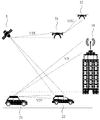
- 1 is an example of an environment in which wireless communication is performed.
- 2 is an example of an antenna device including two dipole antennas.
- 3 is another example of an antenna device including two dipole antennas.
- 4 is another example of an antenna device including two dipole antennas.
- 5 is another example of an antenna device including two dipole antennas.
- 6 is an example of an antenna device including four dipole antennas.
- FIG. 7 is an example of a radiation pattern of the antenna device of FIG. 6.
- FIG. 8 is another example of a radiation pattern of the antenna device of FIG. 6.
- Terms such as 1st, 2nd, A, B, etc. may be used to describe various components, but the components are not limited by the above terms, only for the purpose of distinguishing one component from other components. Is only used.
- a first component may be referred to as a second component, and similarly, a second component may be referred to as a first component.
- the term and/or includes a combination of a plurality of related listed items or any of a plurality of related listed items.
- each constituent part in the present specification is merely divided by the main function that each constituent part is responsible for. That is, two or more constituent parts to be described below may be combined into one constituent part, or one constituent part may be divided into two or more according to more subdivided functions.
- each of the constituent units to be described below may additionally perform some or all of the functions of other constituent units in addition to its own main function, and some of the main functions of each constituent unit are different. It goes without saying that it may be performed exclusively by.
- each of the processes constituting the method may occur differently from the specified order unless a specific order is clearly stated in the context. That is, each process may occur in the same order as the specified order, may be performed substantially simultaneously, or may be performed in the reverse order.
- the vehicle 21 performs vehicle-to-vehicle communication (V2V) with another vehicle 22. Furthermore, vehicles can communicate with infrastructure installed around the road.
- the vehicle 21 communicates with the infrastructure 10 disposed on the building (V2I: Vehicle to Infra).
- the infrastructure 10 may be a device such as an AP that collects surrounding information.
- Vehicle 22 communicates with satellite 5 in the air.
- drones have a similar communication environment.
- the drone 31 can communicate with other drones 32 (U2U: UAV to UAV). In addition, the drone 31 may communicate with the satellite 50. In this way, objects such as vehicles and drones are not on a horizontal plane and can communicate with objects having a large height (altitude) difference.
- the current antenna has a problem that the gain is high only in a limited elevation range.
- the World Radio Conference (WRC) under the International Telecommunication Union (ITU) distributed 5030 to 5150 MHz bands exclusively for ground control of unmanned aerial vehicles worldwide.
- the 5030 ⁇ 5150MHz band was allocated to create an environment that enables communication up to several kilometers.
- the array antenna described below can also serve a 5000MHz band.
- the technique to be described below relates to an array antenna.
- the technology to be described below relates to an array antenna generating multiple beams.
- the technique to be described below relates to an array antenna supporting a wide elevation angle range.
- the array antenna will be briefly described first.
- a single antenna element does not have various radiation patterns. Developers can use array antennas to develop antennas with specific directivity (radiation pattern).
- the array antenna includes an array using two or more antenna elements simultaneously.
- the array antenna may generate a constant radiation pattern by arranging the antenna elements in a certain shape (geometrically).
- antennas There are various types of antennas according to the arrangement of antenna elements.
- a linear array antenna is an antenna in which the center of an array element is arranged along a straight line.
- the spacing between antenna elements may be constant.
- an antenna element constituting the array antenna is assumed to be a dipole antenna.
- the array antenna in addition to a dipole antenna, other types of antennas such as a monopole antenna, a loop antenna, a yagi antenna, a Vivaldi antenna, and a Quasi-yagi antenna may be used.
- the array antenna also generates a desired radiation pattern by controlling the phase of the current supplied to the arrayed antenna elements.
- the array antenna generates a specific radiation pattern by electrically controlling the amplitude and/or phase of a feed signal (current) supplied to the antenna element. Phase adjustment can be performed using a phase shifter. The amplitude can be adjusted using an attenuator.
- the antenna element will be described based on a dipole antenna.
- the antenna device may use another type of antenna.
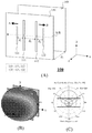
- 2 is an example of an antenna device including two dipole antennas.
- 2(A) is an example of an antenna device 100 comprising two dipole antennas and a parasitic element.
- the antenna device 100 includes a first dipole antenna 111, a second dipole antenna 112, a first parasitic element 121, a second parasitic element 122, and a reflector 140.
- the first dipole antenna 111 and the second dipole antenna 112 transmit and receive signals of a certain band according to performance requirements.
- the first dipole antenna 111 and the second dipole antenna 112 may process a 5GHz band signal.
- the first dipole antenna 111 and the second dipole antenna 112 are disposed on the substrate 130.
- the substrate 130 may be made of a dielectric material.
- a plane in which the first dipole antenna 111 and the second dipole antenna 112 are disposed is referred to as a first XY plane.
- the substrate 130 can be said to be parallel to the XY plane.
- the first dipole antenna 111 and the second dipole antenna 112 are linearly arranged on the substrate 130 along the X axis.
- the centers of the first dipole antenna 111 and the second dipole antenna 112 may be arranged along the X axis.
- Each of the first dipole antenna 111 and the second dipole antenna 112 has a longitudinal direction perpendicular to the X axis.
- d 1 ⁇ /4.
- the lengths of the first dipole antenna 111 and the second dipole antenna 112 may vary depending on the size of the antenna device and the performance of the target antenna device.
- the first parasitic element 121 and the second parasitic element 122 are disposed on the substrate 130.
- the first parasitic element 121 and the second parasitic element 122 are linearly arranged along the X axis on the substrate 130.
- the centers of the first parasitic element 121 and the second parasitic element 122 may be arranged along the X axis.
- Each of the first parasitic element 121 and the second parasitic element 122 has a longitudinal direction perpendicular to the X axis. That is, the first parasitic element 121 and the second parasitic element 122 may be disposed horizontally with the first dipole antenna 111 and the second dipole antenna 112.
- the first parasitic element 121 is disposed at a distance regularly spaced apart from the first dipole antenna 111 in the X-axis outer direction (A direction).
- the second parasitic element 122 is disposed at a distance regularly spaced apart from the second dipole antenna 112 in the X-axis outer direction (B direction).
- the first parasitic element 121 and the second parasitic element 122 may serve as a kind of waveguide.
- the first parasitic element 121 and the second parasitic element 122 allow the beam of the antenna to have a wide elevation angle.
- the length of the parasitic elements 121 and 122 may vary depending on the size of the antenna device and the performance of the target antenna device.
- the reflector 130 is disposed in a direction opposite to the main beam formed by the antenna.
- the distance d 3 between the substrate 130 and the reflector 140 may be within 1/2 wavelength (d 3 ⁇ ⁇ /3).
- the reflector 140 may also be disposed on the XY plane.
- the plane on which the reflector 140 is disposed is referred to as a second XY plane.
- Reflector 140 reduces back lobe gain.
- the reflector 140 allows the beam of the antenna to have a wide elevation angle.
- the reflector 140 may be formed of various shapes or materials used in a typical antenna device.
- the reflector 140 may be made of a metal, ceramic, or PCB material.
- the substrate 130 and the reflector 140 may be connected to each other by a support having a certain shape.
- Fig. 2(A) does not show a power supply device.
- the power supply device may have a line connected to the support and the substrate 130.
- the power feeding device may supply the same power having the same phase to the first dipole antenna 111 and the second dipole antenna 112.
- the power supply device may be implemented in various forms.
- the power supply device may include a half power divider that distributes the input power with the same half power.
- the first dipole antenna 111 and the second dipole antenna 112 receiving power correspond to a radiator.
- Each of the first dipole antenna 111 and the second dipole antenna 112 may emit broad side beams.
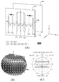
- 2B is an example of a radiation pattern of the antenna device 100.
- 2(C) is an example of a beam pattern of the antenna device 100 in the zy plane (elevation cut).
- Table 1 shows the maximum gain and half power beam width of the antenna device 100. According to the experimental results, it can be seen that the beam width of the antenna device 100 is increased compared to an antenna device (reference) composed of only two dipole antennas. Therefore, the antenna device 100 has a wide elevation angle range. For reference, the antenna device 100 has no parasitic element only.
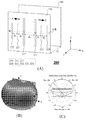
- 3 is another example of an antenna device including two dipole antennas.
- 3(A) is an example of an antenna device 200 comprising two dipole antennas and a parasitic element.
- the antenna device 200 includes a first dipole antenna 211, a second dipole antenna 212, a first parasitic element 221, a second parasitic element 222, a third parasitic element 223, and a fourth parasitic element 224 and a reflector 240.
- the first dipole antenna 211 and the second dipole antenna 212 transmit and receive signals of a certain band according to performance requirements.
- the first dipole antenna 211 and the second dipole antenna 212 may process a 5GHz band signal.
- the first dipole antenna 211 and the second dipole antenna 212 are disposed on the substrate 230.
- the substrate 230 may be made of a dielectric material.
- a plane on which the first dipole antenna 211 and the second dipole antenna 212 are disposed is referred to as a first XY plane.
- the substrate 230 can be said to be parallel to the XY plane.
- the first dipole antenna 211 and the second dipole antenna 212 are linearly arranged on the substrate 230 along the X axis.
- the centers of the first dipole antenna 211 and the second dipole antenna 212 may be arranged along the X axis.
- Each of the first dipole antenna 211 and the second dipole antenna 212 has a longitudinal direction perpendicular to the X axis.
- the lengths of the first dipole antenna 211 and the second dipole antenna 212 may vary depending on the size of the antenna device and the performance of the target antenna device.
- the antenna device 200 includes four parasitic elements.
- the first parasitic element 221, the second parasitic element 222, the third parasitic element 223, and the fourth parasitic element 224 are disposed on the substrate 230.
- the first parasitic element 221, the second parasitic element 222, the third parasitic element 223, and the fourth parasitic element 224 are linearly arranged on the substrate 230 along the X axis.
- the centers of the first parasitic element 221, the second parasitic element 222, the third parasitic element 223, and the fourth parasitic element 224 may be arranged along the X axis.
- Each of the first parasitic element 221, the second parasitic element 222, the third parasitic element 223, and the fourth parasitic element 224 has a longitudinal direction perpendicular to the X-axis. That is, the first parasitic element 221, the second parasitic element 222, the third parasitic element 223, and the fourth parasitic element 224 are the first dipole antenna 211 and the second dipole antenna 212 Can be placed horizontally.
- the first parasitic element 221 is disposed at a distance regularly spaced apart from the first dipole antenna 211 in an X-axis outer direction (A direction).
- the second parasitic element 222 is disposed at a distance regularly spaced apart from the first parasitic element 221 in the X-axis outer direction (A direction).
- the third parasitic element 223 is disposed at a distance regularly spaced apart from the second dipole antenna 212 in the X-axis outer direction (B direction).
- the fourth parasitic element 224 is disposed at a distance regularly spaced apart from the third parasitic element 223 in the X-axis outer direction (B direction).
- the first parasitic element 221, the second parasitic element 222, the third parasitic element 223, and the fourth parasitic element 224 may serve as a kind of waveguide.
- the first parasitic element 221, the second parasitic element 222, the third parasitic element 223, and the fourth parasitic element 224 allow the beam of the antenna to have a wide elevation angle.
- the lengths of the parasitic elements 221, 222, 223, and 224 may vary depending on the size of the antenna device and the performance of the target antenna device.
- the reflector 240 is disposed in a direction opposite to the main beam formed by the antenna.
- the distance d 3 between the substrate 230 and the reflector 240 may be within 1/2 wavelength (d 3 ⁇ ⁇ /3).
- the reflector 240 may also be disposed on the XY plane.
- the plane on which the reflector 240 is disposed is referred to as a second XY plane.
- Reflector 240 reduces back lobe gain.
- the reflector 240 allows the beam of the antenna to have a wide elevation angle.
- the reflector 240 may be formed of various shapes or materials used in a typical antenna device.
- the reflector 240 may be made of metal, ceramic, or PCB material.
- the substrate 230 and the reflector 240 may be connected to a support having a certain shape.
- Fig. 3(A) does not show a power supply device.
- the power supply device may have a line connected to the support and the substrate 230.
- the power feeding device may supply the same power having the same phase to the first dipole antenna 211 and the second dipole antenna 212.
- the power supply device may be implemented in various forms.
- the power supply device may include a half power divider that distributes the input power with the same half power.
- the first dipole antenna 211 and the second dipole antenna 212 receiving power correspond to a radiator.
- Each of the first dipole antenna 211 and the second dipole antenna 212 may emit a broad side beam.
- 3(B) is an example of a radiation pattern of the antenna device 200.
- 3(C) is an example of a beam pattern of the antenna device 200 in the zy plane (elevation plane, elevation cut).
- Table 2 shows the maximum gain and half power beam width of the antenna device 300. According to the experimental results, it can be seen that the beam width of the antenna device 200 is increased compared to the antenna device 100. Accordingly, the antenna device 200 has a wider elevation angle range than the antenna device 100.
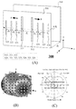
- 4 is another example of an antenna device including two dipole antennas.
- 4(A) is an example of an antenna device 300 comprising two dipole antennas and a parasitic element.
- the antenna device 300 includes a first dipole antenna 311, a second dipole antenna 312, a first parasitic element 321, a second parasitic element 322, a third parasitic element 323, and a fourth parasitic element 324, a fifth parasitic element 325, a sixth parasitic element 326, and a reflector 340.
- the first dipole antenna 311 and the second dipole antenna 312 transmit and receive signals of a certain band according to performance requirements.
- the first dipole antenna 311 and the second dipole antenna 312 may process a 5GHz band signal.
- the first dipole antenna 311 and the second dipole antenna 312 are disposed on the substrate 330.
- the substrate 330 may be made of a dielectric material.
- a plane in which the first dipole antenna 311 and the second dipole antenna 312 are disposed is referred to as a first XY plane.
- the substrate 330 can be said to be parallel to the XY plane.
- the first dipole antenna 311 and the second dipole antenna 312 are linearly arranged on the substrate 330 along the X axis.
- the centers of the first dipole antenna 311 and the second dipole antenna 312 may be arranged along the X axis.
- Each of the first dipole antenna 311 and the second dipole antenna 312 has a longitudinal direction perpendicular to the X axis.
- the lengths of the first dipole antenna 311 and the second dipole antenna 312 may vary depending on the size of the antenna device and the performance of the target antenna device.
- the antenna device 300 includes six parasitic elements.
- the first parasitic element 321, the second parasitic element 322, the third parasitic element 323, the fourth parasitic element 324, the fifth parasitic element 325, and the sixth parasitic element 326 are a substrate ( 330).
- the first parasitic element 321, the second parasitic element 322, the third parasitic element 323, the fourth parasitic element 324, the fifth parasitic element 325, and the sixth parasitic element 326 are a substrate ( 330) are arranged linearly along the X axis.
- the center of the first parasitic element 321, the second parasitic element 322, the third parasitic element 323, the fourth parasitic element 324, the fifth parasitic element 325, and the sixth parasitic element 326 It can be arranged along the X axis.
- the first parasitic element 321, the second parasitic element 322, the third parasitic element 323, the fourth parasitic element 324, the fifth parasitic element 325, and the sixth parasitic element 326 are each length The direction is perpendicular to the X axis. That is, the first parasitic element 321, the second parasitic element 322, the third parasitic element 323, the fourth parasitic element 324, the fifth parasitic element 325, and the sixth parasitic element 326 It may be disposed horizontally with the first dipole antenna 311 and the second dipole antenna 312.
- the first parasitic element 321 is disposed at a distance regularly spaced apart from the first dipole antenna 311 in an X-axis outer direction (A direction).
- the second parasitic element 322 is disposed at a distance regularly spaced apart from the first parasitic element 321 in an X-axis outer direction (A direction). It may be a distance d 2 between the first parasitic element 321 and the second parasitic element 322.
- the third parasitic element 323 is disposed at a distance regularly spaced apart from the second parasitic element 322 in the X-axis outer direction (A direction). It may be a distance d 2 between the third parasitic element 323 and the second parasitic element 322.
- the fourth parasitic element 324 is disposed at a distance regularly spaced apart from the second dipole antenna 312 in the X-axis outer direction (B direction).
- the fifth parasitic element 325 is disposed at a distance regularly spaced apart from the fourth parasitic element 324 in the X-axis outer direction (B direction). It may be a distance d 2 between the fourth parasitic element 324 and the fifth parasitic element 325.
- the sixth parasitic element 326 is disposed at a distance regularly spaced apart from the fifth parasitic element 325 in the X-axis outer direction (B direction). It may be a distance d 2 between the fifth parasitic element 325 and the sixth parasitic element 326.
- the first parasitic element 321, the second parasitic element 322, the third parasitic element 323, the fourth parasitic element 324, the fifth parasitic element 325, and the sixth parasitic element 326 are a kind of waveguide. Can play a role.
- the first parasitic element 321, the second parasitic element 322, the third parasitic element 323, the fourth parasitic element 324, the fifth parasitic element 325, and the sixth parasitic element 326 are Make the beam have a wide elevation angle.
- the lengths of the parasitic elements 321, 322, 323, 324, 325, and 326 may vary depending on the size of the antenna device and the performance of the target antenna device.
- the reflector 340 is disposed in a direction opposite to the main beam formed by the antenna.
- the distance d 3 between the substrate 330 and the reflector 340 may be within 1/2 wavelength (d 3 ⁇ ⁇ /3).
- the reflector 340 may also be disposed on the XY plane.
- the plane on which the reflector 340 is disposed is referred to as a second XY plane.
- Reflector 340 reduces back lobe gain.
- the reflector 340 allows the beam of the antenna to have a wide elevation angle.
- the reflector 340 may be formed of various shapes or materials used in a typical antenna device.
- the reflector 340 may be made of a metal, ceramic, or PCB material.
- the substrate 330 and the reflector 340 may be connected to a support having a certain shape.
- Fig. 4A does not show a power supply device.
- the power supply device may have a line connected to the support and the substrate 330.
- the power feeding device may supply the same power having the same phase to the first dipole antenna 311 and the second dipole antenna 312.
- the power supply device may be implemented in various forms.
- the power supply device may include a half power divider that distributes the input power with the same half power.
- the first dipole antenna 311 and the second dipole antenna 312 receiving power correspond to a radiator.
- Each of the first dipole antenna 311 and the second dipole antenna 312 may emit a broad side beam.
- 4B is an example of a radiation pattern of the antenna device 300.
- 4(C) is an example of a beam pattern of the antenna device 300 in a zy plane (a elevation cut).
- Antenna device 200 4.8dBi 161°
- Antenna device 300 6.1dBi 63°
- Table 3 shows the maximum gain and half power beam width of the antenna device 300. According to the experimental results, the beams radiated by the first dipole antenna 311 and the second dipole antenna 312 in the antenna device 300 are separated.
- the antenna device 200 has a shape of a beam connected in the hemisphere region, thereby providing communication for the hemisphere region.
- 5 is another example of an antenna device including two dipole antennas.
- 5A is an example of an antenna device 400 comprising two dipole antennas and a parasitic element.
- the antenna device 400 includes a first dipole antenna 411, a second dipole antenna 412, a first parasitic element 421, a second parasitic element 422, a third parasitic element 423, and a fourth parasitic element 424, a fifth parasitic element 425, and a reflector 440.
- the first dipole antenna 411 and the second dipole antenna 412 transmit and receive signals of a certain band according to performance requirements.
- the first dipole antenna 411 and the second dipole antenna 412 may process a 5GHz band signal.
- the first dipole antenna 411 and the second dipole antenna 412 are disposed on the substrate 430.
- the substrate 430 may be made of a dielectric material.
- a plane in which the first dipole antenna 411 and the second dipole antenna 412 are disposed is referred to as a first XY plane.
- the substrate 430 can be said to be parallel to the XY plane.
- the first dipole antenna 411 and the second dipole antenna 412 are linearly arranged on the substrate 430 along the X axis.
- the centers of the first dipole antenna 411 and the second dipole antenna 412 may be arranged along the X axis.
- Each of the first dipole antenna 411 and the second dipole antenna 412 has a longitudinal direction perpendicular to the X axis.
- the lengths of the first dipole antenna 411 and the second dipole antenna 412 may vary depending on the size of the antenna device and the performance of the target antenna device.
- the antenna device 400 includes five parasitic elements.
- the first parasitic element 421, the second parasitic element 422, the third parasitic element 423, and the fourth parasitic element 424 are disposed on the substrate 430.
- a fifth parasitic element 425 is disposed on the substrate 430 between the first dipole antenna 411 and the second dipole antenna 412.
- the first parasitic element 421, the second parasitic element 422, the third parasitic element 423, the fourth parasitic element 424, and the fifth parasitic element 425 are linear along the X-axis on the substrate 430. Are arranged as.
- the centers of the first parasitic element 421, the second parasitic element 422, the third parasitic element 423, the fourth parasitic element 424, and the fifth parasitic element 425 may be arranged along the X axis.
- Each of the first parasitic element 421, the second parasitic element 422, the third parasitic element 423, the fourth parasitic element 424, and the fifth parasitic element 425 has a longitudinal direction perpendicular to the X-axis. That is, the first parasitic element 421, the second parasitic element 422, the third parasitic element 423, the fourth parasitic element 424 and the fifth parasitic element 425 are the first dipole antenna 411 and It may be disposed horizontally with the second dipole antenna 412.
- the first parasitic element 421 is disposed at a distance regularly spaced apart from the first dipole antenna 411 in the X-axis outer direction (A direction).
- the second parasitic element 422 is disposed at a distance regularly spaced apart from the first parasitic element 421 in the X-axis outer direction (A direction).
- the third parasitic element 423 is disposed at a distance regularly spaced apart from the second dipole antenna 412 in the X-axis outer direction (B direction).
- the fourth parasitic element 424 is disposed at a distance regularly spaced apart from the third parasitic element 423 in an X-axis outer direction (B direction).
- the fifth parasitic element 425 may be located at the center between the first dipole antenna 411 and the second dipole antenna 412.
- the first parasitic element 421, the second parasitic element 422, the third parasitic element 423, the fourth parasitic element 424, and the fifth parasitic element 425 may serve as a kind of waveguide.
- the first parasitic element 421, the second parasitic element 422, the third parasitic element 423, and the fourth parasitic element 424 have a wide elevation angle of the antenna beam.
- the lengths of the parasitic elements 421, 222, 223, and 224 may vary depending on the size of the antenna device and the performance of the target antenna device.
- the reflector 440 is disposed in a direction opposite to the main beam formed by the antenna.
- the distance d 3 between the substrate 430 and the reflector 440 may be within 1/2 wavelength (d 3 ⁇ ⁇ /3).
- the reflector 440 may also be disposed on the XY plane.
- the plane on which the reflector 440 is disposed is referred to as a second XY plane.
- Reflector 440 reduces back lobe gain.
- the reflector 440 allows the beam of the antenna to have a wide elevation angle.
- the reflector 440 may be formed of various shapes or materials used in a typical antenna device.
- the reflector 440 may be made of metal, ceramic, or PCB material.
- the substrate 430 and the reflector 440 may be connected to a support having a certain shape.
- Fig. 5A does not show a power supply device.
- the power supply device may have a line connected to the support and the substrate 430.
- the power feeding device may supply the same power having the same phase to the first dipole antenna 411 and the second dipole antenna 412.
- the power supply device may be implemented in various forms.
- the power supply device may include a half power divider that distributes the input power with the same half power.
- the first dipole antenna 411 and the second dipole antenna 412 receiving power correspond to a radiator.
- Each of the first dipole antenna 411 and the second dipole antenna 412 may emit a broad side beam.
- 5B is an example of a radiation pattern of the antenna device 400.
- 5(C) is an example of a beam pattern of the antenna device 400 in the zy plane (elevation cut).
- Table 4 shows the maximum gain and half power beam width of the antenna device 400. According to the experimental results, it can be seen that the beam width of the antenna device 400 is increased compared to the antenna device 300. That is, due to the added parasitic element 425, the antenna device 400 has a wider elevation angle range than the antenna device 200.
- the antenna device 500 includes a first dipole antenna 511, a second dipole antenna 512, a third dipole antenna 513, a fourth dipole antenna 514, a first parasitic element 521, and a second parasitic element 522, a third parasitic element 523, a fourth parasitic element 524, and a reflector 540.
- the first dipole antenna 511, the second dipole antenna 512, the third dipole antenna 513, and the fourth dipole antenna 514 transmit and receive signals of a certain band according to performance requirements.
- the first dipole antenna 511, the second dipole antenna 512, the third dipole antenna 513, and the fourth dipole antenna 514 may process a 5GHz band signal.
- the first dipole antenna 511, the second dipole antenna 512, the third dipole antenna 513, and the fourth dipole antenna 514 are disposed on the substrate 530.
- the substrate 530 may be made of a dielectric material.
- a plane on which the first dipole antenna 511, the second dipole antenna 512, the third dipole antenna 513, and the fourth dipole antenna 514 are disposed is referred to as a first XY plane.
- the substrate 530 can be said to be parallel to the XY plane.
- the first dipole antenna 511 and the second dipole antenna 512 are linearly arranged on the substrate 530 along the X axis.
- the centers of the first dipole antenna 511 and the second dipole antenna 512 may be arranged along the X axis.
- Each of the first dipole antenna 511 and the second dipole antenna 512 has a longitudinal direction perpendicular to the X axis.
- d 1 is ⁇ /4.
- the lengths of the first dipole antenna 511 and the second dipole antenna 512 may vary depending on the size of the antenna device and the performance of the target antenna device.
- the third dipole antenna 513 and the fourth dipole antenna 514 are linearly arranged along the Y axis on the substrate 530.
- the centers of the third dipole antenna 513 and the fourth dipole antenna 514 may be arranged along the Y axis.
- Each of the third dipole antenna 513 and the fourth dipole antenna 514 has a longitudinal direction perpendicular to the Y axis.
- the lengths of the third dipole antenna 513 and the fourth dipole antenna 514 may vary depending on the size of the antenna device and the performance of the target antenna device.
- the first parasitic element 521 and the second parasitic element 522 are linearly arranged along the X axis on the substrate 530.
- the centers of the first parasitic element 521 and the second parasitic element 522 may be arranged along the X axis.
- Each of the first parasitic element 521 and the second parasitic element 522 has a longitudinal direction perpendicular to the X axis. That is, the first parasitic element 521 and the second parasitic element 522 may be disposed horizontally with the first dipole antenna 511 and the second dipole antenna 512.
- the first parasitic element 521 is disposed at a distance regularly spaced apart from the first dipole antenna 511 in the X-axis outer direction (A direction).
- the second parasitic element 522 is disposed at a distance regularly spaced apart from the second dipole antenna 512 in the X-axis outer direction (B direction).
- the third parasitic element 523 and the fourth parasitic element 524 are linearly arranged along the Y axis on the substrate 530.
- the centers of the third parasitic element 523 and the fourth parasitic element 524 may be arranged along the Y axis.
- Each of the third parasitic element 523 and the fourth parasitic element 524 has a longitudinal direction perpendicular to the Y axis. That is, the third parasitic element 523 and the fourth parasitic element 522 may be disposed horizontally with the third dipole antenna 513 and the fourth dipole antenna 514.
- the third parasitic element 523 is disposed at a distance regularly spaced apart from the third dipole antenna 513 in the Y-axis outer direction (C direction).
- the fourth parasitic element 524 is disposed at a distance regularly spaced apart from the fifth dipole antenna 515 in the Y-axis outer direction (D direction).
- the first parasitic element 521, the second parasitic element 522, the third parasitic element 523, and the fourth parasitic element 524 may serve as a kind of waveguide.
- the first parasitic element 521, the second parasitic element 522, the third parasitic element 523, and the fourth parasitic element 524 allow the beam of the antenna to have a wide elevation angle.
- the length of the parasitic elements 521, 522, 523, and 524 may vary depending on the size of the antenna device and the performance of the target antenna device.
- the reflector 530 is disposed in a direction opposite to the main beam formed by the antenna.
- the distance d 3 between the substrate 530 and the reflector 540 may be within 1/2 wavelength (d 3 ⁇ ⁇ /3).
- the reflector 540 may also be disposed on the XY plane.
- the plane on which the reflector 540 is disposed is referred to as a second XY plane.
- Reflector 540 reduces back lobe gain.
- the reflector 540 allows the beam of the antenna to have a wide elevation angle.
- the reflector 540 may be formed of various shapes or materials used in a typical antenna device.
- the reflector 540 may be made of a metal, ceramic, or PCB material.
- the substrate 530 and the reflector 540 may be connected to each other by a support having a certain shape. 6 does not show a power supply device.
- the power supply device may have a line connected to the support and the substrate 530.
- the power feeding device supplies constant power to the first dipole antenna 511, the second dipole antenna 512, the third dipole antenna 513, and the fourth dipole antenna 514.
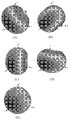
- 7 is an example of a radiation pattern of the antenna device 500 of FIG. 6.
- 7 is an example of radiation patterns for the beam patterns shown in Table 5 below.
- 7(A) is an example of a radiation pattern for beam pattern 1.
- 7(B) is an example of a radiation pattern for beam pattern 2.
- 7(C) is an example of a radiation pattern for beam pattern 3;
- 7(D) is an example of a radiation pattern for beam pattern 4.
- 7(E) is an example of a radiation pattern for all beams in which beam patterns 1 to 4 are combined.
- the antenna device 500 has a maximum gain of 5.1dBi.
- Beam pattern First dipole antenna phase 2nd dipole antenna phase 3rd dipole antenna phase 4th dipole antenna phase Beam pattern 1 0° 0° 150° 60° Beam pattern 2 0° 0° 60° 150° Beam pattern 3 150° 60° 0° 0° Beam pattern 4 60° 150° 0° 0°
- the power feeding device applies power of the same power to the first dipole antenna 511, the second dipole antenna 512, the third dipole antenna 513, and the fourth dipole antenna 514.
- the power supply device may include a power divider that equally distributes the input power.
- the power feeding device may apply power of different phases to individual dipole antennas using a coupler or a hybrid coupler.
- the first dipole antenna 511, the second dipole antenna 512, the third dipole antenna 513, and the fourth dipole antenna 514 may be divided into two sets.
- the first antenna set includes a first dipole antenna 511 and a second dipole antenna 512.
- the second antenna set includes a third dipole antenna 513 and a fourth dipole antenna 514.
- the power feeding device applies power of the same phase to the first dipole antenna 511 and the second dipole antenna 512 included in the first antenna set.
- the power feeding device applies power of the same phase 0° to the first dipole antenna 511 and the second dipole antenna 512.
- the power feeding device applies power having a phase different from that of the first antenna set to the second antenna set.
- the power supply device applies power of different phases to the third dipole antenna 513 and the fourth dipole antenna 514.
- the power feeding device may apply power of 150° phase to the third dipole antenna 511 and apply power of 60° phase to the fourth dipole antenna 514.
- the power feeding device applies power of the same phase to the first dipole antenna 511 and the second dipole antenna 512 included in the first antenna set.
- the power feeding device applies power of the same phase 0° to the first dipole antenna 511 and the second dipole antenna 512.
- the power feeding device applies power having a phase different from that of the first antenna set to the second antenna set.
- the power supply device applies power of different phases to the third dipole antenna 513 and the fourth dipole antenna 514.
- the power feeding device may apply power of 60° phase to the third dipole antenna 511 and apply power of 150° phase to the fourth dipole antenna 514.
- the power feeding device applies power of the same phase to the first dipole antenna 511 and the second dipole antenna 512 included in the first antenna set.
- the power feeding device applies power of different phases to the first dipole antenna 511 and the second dipole antenna 512.
- the power feeding device may apply power of 150° phase to the first dipole antenna 511 and apply power of 60° phase to the second dipole antenna 512.
- the power feeding device applies power having a phase different from that of the first antenna set to the second antenna set.
- the power feeding device applies power of the same phase to the third dipole antenna 513 and the fourth dipole antenna 514.
- the power feeding device applies power of the same phase 0° to the third dipole antenna 513 and the fourth dipole antenna 514.
- the power feeding device applies power of the same phase to the first dipole antenna 511 and the second dipole antenna 512 included in the first antenna set.
- the power feeding device applies power of different phases to the first dipole antenna 511 and the second dipole antenna 512.
- the power feeding device may apply power of 60° phase to the first dipole antenna 511 and apply power of 150° phase to the second dipole antenna 512.
- the power feeding device applies power having a phase different from that of the first antenna set to the second antenna set.
- the power feeding device applies power of the same phase to the third dipole antenna 513 and the fourth dipole antenna 514.
- the power feeding device applies power of the same phase 0° to the third dipole antenna 513 and the fourth dipole antenna 514.
- the power feeding device may generate an entire radiation pattern such as 7(E) while repeating the power feeding method in which the beam patterns 1 to 4 are generated over time.
- 8 is another example of a radiation pattern of the antenna device of FIG. 6.
- 8 is an example of radiation patterns for the beam patterns shown in Table 6 below.
- 8(A) is an example of a radiation pattern for beam pattern 1.
- 8(B) is an example of a radiation pattern for beam pattern 2;
- 8(C) is an example of a radiation pattern for beam pattern 3;
- 8(D) is an example of a radiation pattern for beam pattern 4.
- 8(E) is an example of a radiation pattern for all beams in which beam patterns 1 to 4 are combined.
- the antenna device 500 has a maximum gain of 5.5dBi.
- Beam pattern First dipole antenna phase 2nd dipole antenna phase 3rd dipole antenna phase 4th dipole antenna phase Beam pattern 1 0° 0° 0° 0° Beam pattern 2 0° 0° 180° 180° Beam pattern 3 0° 0° - - Beam pattern 4 - - 0° 0°
- the first dipole antenna 511, the second dipole antenna 512, the third dipole antenna 513, and the fourth dipole antenna 514 may be divided into two sets.
- the first antenna set includes a first dipole antenna 511 and a second dipole antenna 512.
- the second antenna set includes a third dipole antenna 513 and a fourth dipole antenna 514.
- the power feeding device may apply power of the same power to the first dipole antenna 511, the second dipole antenna 512, the third dipole antenna 513, and the fourth dipole antenna 514. Furthermore, the power feeding device may not apply power to any one of the first antenna set and the second antenna set.
- the power supply device may include a power divider that equally distributes the input power.
- the power feeding device may apply power of different phases to individual dipole antennas using a coupler or a hybrid coupler.
- the power feeding device applies power of the same phase to the first dipole antenna 511, the second dipole antenna 512, the third dipole antenna 513, and the fourth dipole antenna 514.
- the power feeding device applies power of the same phase 0° to the first dipole antenna 511, the second dipole antenna 512, the third dipole antenna 513, and the fourth dipole antenna 514.
- the power feeding device applies power of the same phase to the first dipole antenna 511 and the second dipole antenna 512 included in the first antenna set.
- the power feeding device applies power of the same phase 0° to the first dipole antenna 511 and the second dipole antenna 512.
- the power feeding device applies power having a phase different from that of the first antenna set to the second antenna set.
- the power supply device may apply power of the same phase to the third dipole antenna 513 and the fourth dipole antenna 514.
- the power feeding device may apply power of 180° phase to the third dipole antenna 513 and the fourth dipole antenna 514.
- the power feeding device applies power of the same phase to the first dipole antenna 511 and the second dipole antenna 512 included in the first antenna set.
- the power feeding device applies power of the same phase 0° to the first dipole antenna 511 and the second dipole antenna 512.
- the power supply device may not apply power to the third dipole antenna 513 and the fourth dipole antenna 514.
- the power feeding device applies power of the same phase to the third dipole antenna 513 and the fourth dipole antenna 514 included in the second antenna set.
- the power feeding device applies power of the same phase 0° to the third dipole antenna 513 and the fourth dipole antenna 514.
- the power supply device may not apply power to the first dipole antenna 511 and the second dipole antenna 512.
- the power feeding device may generate an entire radiation pattern such as 8 (E) by repeating the power feeding method in which the beam patterns 1 to 4 are generated over time.
- the power supply method of the power supply device described above may be implemented as a program (or application) including an executable algorithm that can be executed on a computer.
- the program may be provided by being stored in a non-transitory computer readable medium.
- the non-transitory readable medium refers to a medium that stores data semi-permanently and can be read by a device, not a medium that stores data for a short moment, such as a register, cache, or memory.
Landscapes
- Aerials With Secondary Devices (AREA)
- Variable-Direction Aerials And Aerial Arrays (AREA)
Abstract
광범위 앙각을 갖는 안테나 장치는 제1 빔을 방사하는 제1 안테나, 상기 제1 안테나가 배치되는 평면에서 상기 제1 안테나로부터 X축 방향으로 1/4 파장 간격으로 선형 배치되며, 제2 빔을 방사하는 제2 안테나, 상기 평면에서 상기 제1 안테나로부터 X축 외측 방향으로 1/8 파장 간격에 선형 배치되는 적어도 하나의 제1 기생소자, 상기 평면에서 상기 제2 안테나로부터 X축 외측 방향으로 1/8 파장 간격에 선형 배치되는 적어도 하나의 제2 기생소자, 상기 평면으로부터 1/2 파장 이내의 간격을 갖는 다른 평면에 배치되는 반사기 및 상기 제1 안테나와 상기 제2 안테나에 동일 위상의 전력을 공급하는 급전 장치를 포함한다.
Description
이하 설명하는 기술은 넓은 앙각을 갖는 안테나에 관한 것이다.
무선 통신 환경 발전과 변화에 따라 다양한 안테나가 연구되었다. 종래 안테나는 주로 방위각면에서 넓은 범위를 서비스하는 기술에 초점이 있었다. 최근 안테나 기술은 방위각뿐만 아니라 앙각(elevation)에 대한 정밀한 빔 포밍 또는 넓은 앙각 범위에 대한 요구가 증가하고 있다. 예컨대, 5G 통신을 위한 3D 빔포밍 기술은 앙각 범위에서도 정밀한 빔포밍이 필요하다. 나아가 IoT 서비스 등장과 함께 서로 높낮이가 다른 객체 사이의 통신 필요성이 증가하고 있다.
종래 안테나는 넓은 앙각에서는 이득이 감소하는 구조를 갖는다. 따라서 넓은 앙각 범위에서 이득이 높은 안테나가 요구되고 있다. 이하 설명하는 기술은 기생소자를 이용하여 넓은 앙각의 브로드 사이드 (broadside) 빔을 갖는 안테나 장치를 제공하고자 한다.
광범위 앙각을 갖는 안테나 장치는 제1 빔을 방사하는 제1 안테나, 상기 제1 안테나가 배치되는 평면에서 상기 제1 안테나로부터 X축 방향으로 1/4 파장 간격으로 선형 배치되며, 제2 빔을 방사하는 제2 안테나, 상기 평면에서 상기 제1 안테나로부터 X축 외측 방향으로 1/8 파장 간격에 선형 배치되는 적어도 하나의 제1 기생소자, 상기 평면에서 상기 제2 안테나로부터 X축 외측 방향으로 1/8 파장 간격에 선형 배치되는 적어도 하나의 제2 기생소자, 상기 평면으로부터 1/2 파장 이내의 간격을 갖는 다른 평면에 배치되는 반사기 및 상기 제1 안테나와 상기 제2 안테나에 동일 위상의 전력을 공급하는 급전 장치를 포함한다.
다른 측면에서 광범위 앙각을 갖는 안테나 장치는 제1 빔을 방사하며, 평면에서 X축 상에 선형 배치되는 제1 안테나 및 제2 빔을 방사하면, 상기 평면에서 상기 제1 안테나로부터 X축 방향으로 1/4 파장 간격을 갖고 X축 상에 선형 배치되는 제2 안테나를 포함하는 제1 안테나 세트, 제3 빔을 방사하며, 상기 평면에서 Y축 상에 선형 배치되는 제3 안테나 및 제4 빔을 방사하면, 상기 평면에서 상기 제3 안테나로부터 X축 방향으로 1/4 파장 간격을 갖고 Y축 상에 선형 배치되는 제4 안테나를 포함하는 제2 안테나 세트, 상기 평면에서 상기 제1 안테나로부터 X축 외측 방향으로 1/8 파장 간격에 선형 배치되는 적어도 하나의 제1 기생소자, 상기 평면에서 상기 제2 안테나로부터 X축 외측 방향으로 1/8 파장 간격에 선형 배치되는 적어도 하나의 제2 기생소자, 상기 평면에서 상기 제3 안테나로부터 Y축 외측 방향으로 1/8 파장 간격에 선형 배치되는 적어도 하나의 제3 기생소자, 상기 평면에서 상기 제4 안테나로부터 Y축 외측 방향으로 1/8 파장 간격에 선형 배치되는 적어도 하나의 제4 기생소자, 상기 평면으로부터 1/2 파장 이내의 간격을 갖는 다른 평면에 배치되는 반사기 및 상기 제1 안테나 세트 및 상기 제2 안테나 세트 중 적어도 하나에 동일 위상의 전력을 공급하는 급전 장치를 포함한다.
이하 설명하는 기술은 선형 배열 안테나와 기생소자를 이용하여 넓은 앙각을 갖는 브로드 사이드 빔을 형성한다. 이를 통해 이하 설명하는 기술은 넓은 앙각 범위에 대한 커버리지(coverage)를 제공할 수 있다.
도 1은 무선 통신을 수행하는 환경에 대한 예이다.
도 2는 2개의 다이폴 안테나를 포함하는 안테나 장치에 대한 예이다.
도 3은 2개의 다이폴 안테나를 포함하는 안테나 장치에 대한 다른 예이다.
도 4는 2개의 다이폴 안테나를 포함하는 안테나 장치에 대한 또 다른 예이다.
도 5는 2개의 다이폴 안테나를 포함하는 안테나 장치에 대한 또 다른 예이다.
도 6은 4개의 다이폴 안테나를 포함하는 안테나 장치에 대한 예이다.
도 7은 도 6의 안테나 장치의 방사 패턴에 대한 예이다.
도 8은 도 6의 안테나 장치의 방사 패턴에 대한 다른 예이다.
이하 설명하는 기술은 다양한 변경을 가할 수 있고 여러 가지 실시례를 가질 수 있는 바, 특정 실시례들을 도면에 예시하고 상세하게 설명하고자 한다. 그러나, 이는 이하 설명하는 기술을 특정한 실시 형태에 대해 한정하려는 것이 아니며, 이하 설명하는 기술의 사상 및 기술 범위에 포함되는 모든 변경, 균등물 내지 대체물을 포함하는 것으로 이해되어야 한다.
제1, 제2, A, B 등의 용어는 다양한 구성요소들을 설명하는데 사용될 수 있지만, 해당 구성요소들은 상기 용어들에 의해 한정되지는 않으며, 단지 하나의 구성요소를 다른 구성요소로부터 구별하는 목적으로만 사용된다. 예를 들어, 이하 설명하는 기술의 권리 범위를 벗어나지 않으면서 제1 구성요소는 제2 구성요소로 명명될 수 있고, 유사하게 제2 구성요소도 제1 구성요소로 명명될 수 있다. 및/또는 이라는 용어는 복수의 관련된 기재된 항목들의 조합 또는 복수의 관련된 기재된 항목들 중의 어느 항목을 포함한다.
본 명세서에서 사용되는 용어에서 단수의 표현은 문맥상 명백하게 다르게 해석되지 않는 한 복수의 표현을 포함하는 것으로 이해되어야 하고, "포함한다" 등의 용어는 설시된 특징, 개수, 단계, 동작, 구성요소, 부분품 또는 이들을 조합한 것이 존재함을 의미하는 것이지, 하나 또는 그 이상의 다른 특징들이나 개수, 단계 동작 구성요소, 부분품 또는 이들을 조합한 것들의 존재 또는 부가 가능성을 배제하지 않는 것으로 이해되어야 한다.
도면에 대한 상세한 설명을 하기에 앞서, 본 명세서에서의 구성부들에 대한 구분은 각 구성부가 담당하는 주기능 별로 구분한 것에 불과함을 명확히 하고자 한다. 즉, 이하에서 설명할 2개 이상의 구성부가 하나의 구성부로 합쳐지거나 또는 하나의 구성부가 보다 세분화된 기능별로 2개 이상으로 분화되어 구비될 수도 있다. 그리고 이하에서 설명할 구성부 각각은 자신이 담당하는 주기능 이외에도 다른 구성부가 담당하는 기능 중 일부 또는 전부의 기능을 추가적으로 수행할 수도 있으며, 구성부 각각이 담당하는 주기능 중 일부 기능이 다른 구성부에 의해 전담되어 수행될 수도 있음은 물론이다.
또, 방법 또는 동작 방법을 수행함에 있어서, 상기 방법을 이루는 각 과정들은 문맥상 명백하게 특정 순서를 기재하지 않은 이상 명기된 순서와 다르게 일어날 수 있다. 즉, 각 과정들은 명기된 순서와 동일하게 일어날 수도 있고 실질적으로 동시에 수행될 수도 있으며 반대의 순서대로 수행될 수도 있다.
도 1은 무선 통신을 수행하는 환경에 대한 예이다. 도 1은 무선 통신을 위한 안테나가 사용되는 환경에 대한 예이다. 도 1은 IoT 환경 중 자율주행 차량과 드론에 대한 예를 도시한다. 차량(21)은 다른 차량(22)과 차량 간 통신(V2V:Vehicle to Vehicle)을 수행한다. 나아가 차량은 도로주변에 설치된 인프라와 통신할 수 있다. 차량(21)은 건물 위에 배치된 인프라(10)와 통신(V2I:Vehicle to Infra)한다. 인프라(10)는 주변 정보를 수집하는 AP와 같은 장치일 수 있다. 차량(22)은 공중에 있는 위성(5)과 통신을 한다. 한편, 드론도 유사한 통신 환경을 갖는다. 드론(31)은 다른 드론(32)과 통신할 수 있다(U2U: UAV to UAV). 또 드론(31)은 위성(50)과 통신을 할 수도 있다. 이와 같이 차량이나 드론과 같은 객체는 수평면에 있지 않고, 높이(고도) 차이가 큰 객체와 통신을 할 수 있다. 다만, 현재 안테나는 제한된 앙각 범위에서만 이득이 높다는 문제가 있다.
최근 국제전기통신연합(ITU, International Telecommunication Union) 산하의 세계 전파통신회의(WRC, World Radio Conference)는 전세계적으로 무인항공기 지상제어 전용으로 5030~5150MHz 대역을 분배하였다. 지상의 무인 항공기 제어 목적으로 5030~5150MHz 대역을 할당하여 수 km까지 통신이 가능하도록 환경을 조성하였다. 이하 설명하는 배열 안테나도 5000MHz 대역 서비스가 가능하다.
이하 설명하는 기술은 배열 안테나에 관한 것이다. 이하 설명하는 기술은 다중 빔을 생성하는 배열 안테나에 관한 것이다. 이하 설명하는 기술은 넓은 앙각 범위를 지원하는 배열 안테나에 관한 것이다. 배열 안테나에 대하여 먼저 간략하게 설명한다.
단일 안테나 소자는 다양한 방사 패턴을 갖지 못한다. 개발자는 특정한 지향성(방사 패턴)을 갖는 안테나를 개발하고자 할 때 배열 안테나를 사용할 수 있다. 배열 안테나는 2개 이상의 안테나 소자를 동시에 사용한 배열을 포함한다.
배열 안테나는 안테나 소자를 일정한 형태로(기하학적으로) 배열하여 일정한 방사 패턴을 생성할 수 있다. 안테나 소자의 배열 형태에 따라 다양한 종류의 안테나가 있다. 예컨대, 선형 배열 안테나(linear array antenna)는 배열 소자 중심이 직선을 따라 배치되는 안테나이다. 선형 배열 안테나에서 안테나 소자 사이의 간격을 일정할 수 있다.
이하 배열 안테나를 구성하는 안테나 요소를 다이폴 안테나로 가정하고 설명한다. 다만, 배열 안테나는 다이폴 안테나 외에 모노폴 안테나, 루프 안테나, 야기 안테나, 비발디 안테나(Vivaldi antenna), 준-야기 안테나 (Quasi-yagi antenna) 등과 같은 다른 유형의 안테나가 사용될 수도 있다.
배열 안테나는 배열된 안테나 소자에 공급되는 전류 위상을 제어하여 원하는 방사 패턴을 생성하기도 한다. 배열 안테나는 안테나 소자에 공급되는 급전 신호(전류)의 진폭 및/또는 위상을 전기적으로 제어하여 특정한 방사 패턴을 생성한다. 위상 조정은 위상 변환기(Phase Shifter)를 이용할 수 있다. 진폭 조정은 감쇠기(Attenuator)를 이용할 수 있다.
이하 안테나 소자는 다이폴 안테나를 기준으로 설명한다. 다만, 전술한 바와 같이 안테나 장치는 다른 유형의 안테나를 사용할 수도 있다.
제1 실시예
도 2는 2개의 다이폴 안테나를 포함하는 안테나 장치에 대한 예이다. 도 2(A)는 2개의 다이폴 안테나와 기생 소자로 구성되는 안테나 장치(100)에 대한 예이다.
안테나 장치(100)는 제1 다이폴 안테나(111), 제2 다이폴 안테나(112), 제1 기생소자(121), 제2 기생소자(122) 및 반사기(140)를 포함한다.
제1 다이폴 안테나(111) 및 제2 다이폴 안테나(112)는 성능 요구에 따라 일정한 대역의 신호를 송수신한다. 예컨대, 제1 다이폴 안테나(111) 및 제2 다이폴 안테나(112)는 5GHz 대역 신호를 처리할 수 있다.
제1 다이폴 안테나(111) 및 제2 다이폴 안테나(112)는 기판(130)에 배치된다. 기판(130)은 유전체 소재로 구성될 수 있다. 설명의 편의를 위하여 제1 다이폴 안테나(111) 및 제2 다이폴 안테나(112)가 배치되는 평면을 제1 XY 평면이라고 명명한다. 이 경우 기판(130)은 XY 평면에 평행하다고 할 수 있다. 제1 다이폴 안테나(111) 및 제2 다이폴 안테나(112)는 기판(130)상에 X축을 따라 선형으로 배열된다. 제1 다이폴 안테나(111) 및 제2 다이폴 안테나(112)의 중심이 X 축을 따라 배열될 수 있다. 제1 다이폴 안테나(111) 및 제2 다이폴 안테나(112) 각각은 길이방향이 X축과 수직이다. 제1 다이폴 안테나(111) 및 제2 다이폴 안테나(112) 사이의 거리 d1는 1/4 파장(d1 = λ/4)일 수 있다. 이하 d1는 λ/4라고 전제한다. 제1 다이폴 안테나(111) 및 제2 다이폴 안테나(112)의 길이는 안테나 장치의 크기, 목표하는 안테나 장치의 성능 등에 따라 달라질 수 있다.
제1 기생소자(121) 및 제2 기생소자(122)는 기판(130)에 배치된다. 제1 기생소자(121) 및 제2 기생소자(122)는 기판(130)상에 X축을 따라 선형으로 배열된다. 제1 기생소자(121) 및 제2 기생소자(122)의 중심이 X 축을 따라 배열될 수 있다. 제1 기생소자(121) 및 제2 기생소자(122) 각각은 길이방향이 X축과 수직이다. 즉, 제1 기생소자(121) 및 제2 기생소자(122)는 제1 다이폴 안테나(111) 및 제2 다이폴 안테나(112)와 수평하게 배치될 수 있다.
제1 기생소자(121)는 제1 다이폴 안테나(111)로부터 X축 외측 방향(A 방향)으로 일정하게 이격된 거리에 배치된다. 제1 기생소자(121)와 제1 다이폴 안테나(111) 사이의 거리 d2는 1/8 파장(d2 = λ/8)일 수 있다. 제2 기생소자(122)는 제2 다이폴 안테나(112)로부터 X축 외측 방향(B 방향)으로 일정하게 이격된 거리에 배치된다. 제2 기생소자(122)와 제2 다이폴 안테나(112) 사이의 거리 d2는 1/8 파장(d2 = λ/8)일 수 있다.
제1 기생소자(121) 및 제2 기생소자(122)는 일종의 도파기 역할을 할 수 있다. 제1 기생소자(121) 및 제2 기생소자(122)는 안테나의 빔이 넓은 앙각을 갖게 한다. 기생소자(121, 122)의 길이는 안테나 장치의 크기, 목표하는 안테나 장치의 성능 등에 따라 달라질 수 있다.
반사기(130)는 안테나가 형성하는 주된 빔의 반대 방향에 배치된다. 기판(130)과 반사기(140) 사이의 거리 d3는 1/2 파장 이내(d3 ≤ λ/3)일 수 있다. 예컨대, d3는 1/3 파장(d3 = λ/3)일 수 있다. 반사기(140)도 XY 평면에 배치될 수 있다. 반사기(140)가 배치되는 평면을 제2 XY 평면이라고 명명한다. 반사기(140)는 후엽(back lobe) 이득을 줄인다. 나아가 반사기(140)는 안테나의 빔이 넓은 앙각을 갖게 한다. 반사기(140)는 통상적인 안테나 장치에 사용되는 다양한 형태 내지 재질로 구성될 수 있다. 예컨대, 반사기(140)는 금속, 세라믹 또는 PCB 재질로 구성될 수 있다.
도 2(A)에 도시하지 않았지만, 기판(130)과 반사기(140)는 일정한 형태의 지지대로 연결될 수 있다. 도 2(A)는 급전 장치를 도시하지 않고 있다. 급전 장치는 지지대와 기판(130)에 연결되는 선로를 가질 수 있다. 기본적으로 급전 장치는 제1 다이폴 안테나(111) 및 제2 다이폴 안테나(112)에 동일한 위상을 갖는 동일한 전력을 공급할 수 있다. 다양한 형태로 급전 장치가 구현될 수 있다. 예컨대, 급전 장치는 입력 전력을 동일한 반전력으로 분배하는 반 전력 분배기를 포함할 수 있다. 전력을 공급받는 제1 다이폴 안테나(111) 및 제2 다이폴 안테나(112)는 방사기에 해당한다. 제1 다이폴 안테나(111) 및 제2 다이폴 안테나(112)는 각각 브로드 사이드 빔을 방사할 수 있다.
도 2(B)는 안테나 장치(100)의 방사 패턴에 대한 예이다. 도 2(C)는 zy 평면(앙각 평면, elevation cut)에서 안테나 장치(100)의 빔 패턴을 도시한 예이다.
| 최대 이득 | 반 전력 빔폭 | |
| 2개의 다이폴 안테나(reference) | 5.95dBi | 104° |
| 안테나 장치(100) | 6.1dBi | 116° |
상기 표 1은 안테나 장치(100)의 최대 이득 및 반 전력 빔 폭을 나타낸다. 실험 결과에 따르면 2개의 다이폴 안테나만으로 구성된 안테나 장치(reference)보다 안테나 장치(100)의 빔 폭이 증가된 것을 알 수 있다. 따라서 안테나 장치(100)는 넓은 앙각 범위를 갖는다. 참고로 안테나 장치(reference)는 안테나 장치(100)에서 기생소자만 없는 형태이다.
제2 실시예
도 3은 2개의 다이폴 안테나를 포함하는 안테나 장치에 대한 다른 예이다. 도 3(A)는 2개의 다이폴 안테나와 기생 소자로 구성되는 안테나 장치(200)에 대한 예이다.
안테나 장치(200)는 제1 다이폴 안테나(211), 제2 다이폴 안테나(212), 제1 기생소자(221), 제2 기생소자(222), 제3 기생소자(223), 제4 기생소자(224) 및 반사기(240)를 포함한다.
제1 다이폴 안테나(211) 및 제2 다이폴 안테나(212)는 성능 요구에 따라 일정한 대역의 신호를 송수신한다. 예컨대, 제1 다이폴 안테나(211) 및 제2 다이폴 안테나(212)는 5GHz 대역 신호를 처리할 수 있다.
제1 다이폴 안테나(211) 및 제2 다이폴 안테나(212)는 기판(230)에 배치된다. 기판(230)은 유전체 소재로 구성될 수 있다. 설명의 편의를 위하여 제1 다이폴 안테나(211) 및 제2 다이폴 안테나(212)가 배치되는 평면을 제1 XY 평면이라고 명명한다. 이 경우 기판(230)은 XY 평면에 평행하다고 할 수 있다. 제1 다이폴 안테나(211) 및 제2 다이폴 안테나(212)는 기판(230)상에 X축을 따라 선형으로 배열된다. 제1 다이폴 안테나(211) 및 제2 다이폴 안테나(212)의 중심이 X 축을 따라 배열될 수 있다. 제1 다이폴 안테나(211) 및 제2 다이폴 안테나(212) 각각은 길이방향이 X축과 수직이다. 제1 다이폴 안테나(211) 및 제2 다이폴 안테나(212) 사이의 거리 d1는 1/4 파장(d1 = λ/4)일 수 있다. 제1 다이폴 안테나(211) 및 제2 다이폴 안테나(212)의 길이는 안테나 장치의 크기, 목표하는 안테나 장치의 성능 등에 따라 달라질 수 있다.
안테나 장치(200)는 4개의 기생소자를 포함한다. 제1 기생소자(221), 제2 기생소자(222), 제3 기생소자(223) 및 제4 기생소자(224)는 기판(230)에 배치된다. 제1 기생소자(221), 제2 기생소자(222), 제3 기생소자(223) 및 제4 기생소자(224)는 기판(230)상에 X축을 따라 선형으로 배열된다. 제1 기생소자(221), 제2 기생소자(222), 제3 기생소자(223) 및 제4 기생소자(224)의 중심이 X 축을 따라 배열될 수 있다. 제1 기생소자(221), 제2 기생소자(222), 제3 기생소자(223) 및 제4 기생소자(224) 각각은 길이방향이 X축과 수직이다. 즉, 제1 기생소자(221), 제2 기생소자(222), 제3 기생소자(223) 및 제4 기생소자(224)는 제1 다이폴 안테나(211) 및 제2 다이폴 안테나(212)와 수평하게 배치될 수 있다.
제1 기생소자(221)는 제1 다이폴 안테나(211)로부터 X축 외측 방향(A 방향)으로 일정하게 이격된 거리에 배치된다. 제1 기생소자(221)와 제1 다이폴 안테나(211) 사이의 거리 d2는 1/8 파장(d2 = λ/8)일 수 있다. 제2 기생소자(222)는 제1 기생소자(221)로부터 X축 외측 방향(A 방향)으로 일정하게 이격된 거리에 배치된다. 제1 기생소자(221)와 제2 기생소자(222) 사이의 거리 d2는 1/8 파장(d2 = λ/8)일 수 있다.
제3 기생소자(223)는 제2 다이폴 안테나(212)로부터 X축 외측 방향(B 방향)으로 일정하게 이격된 거리에 배치된다. 제3 기생소자(223)와 제2 다이폴 안테나(212) 사이의 거리 d2는 1/8 파장(d2 = λ/8)일 수 있다. 제4 기생소자(224)는 제3 기생소자(223)로부터 X축 외측 방향(B 방향)으로 일정하게 이격된 거리에 배치된다. 제3 기생소자(223)와 제4 기생소자(224) 사이의 거리 d2는 1/8 파장(d2 = λ/8)일 수 있다.
제1 기생소자(221), 제2 기생소자(222), 제3 기생소자(223) 및 제4 기생소자(224)는 일종의 도파기 역할을 할 수 있다. 제1 기생소자(221), 제2 기생소자(222), 제3 기생소자(223) 및 제4 기생소자(224)는 안테나의 빔이 넓은 앙각을 갖게 한다. 기생소자(221, 222, 223, 224)의 길이는 안테나 장치의 크기, 목표하는 안테나 장치의 성능 등에 따라 달라질 수 있다.
반사기(240)는 안테나가 형성하는 주된 빔의 반대 방향에 배치된다. 기판(230)과 반사기(240) 사이의 거리 d3는 1/2 파장 이내(d3 ≤ λ/3)일 수 있다. 예컨대, d3는 1/3 파장(d3 = λ/3)일 수 있다. 반사기(240)도 XY 평면에 배치될 수 있다. 반사기(240)가 배치되는 평면을 제2 XY 평면이라고 명명한다. 반사기(240)는 후엽(back lobe) 이득을 줄인다. 나아가 반사기(240)는 안테나의 빔이 넓은 앙각을 갖게 한다. 반사기(240)는 통상적인 안테나 장치에 사용되는 다양한 형태 내지 재질로 구성될 수 있다. 예컨대, 반사기(240)는 금속, 세라믹 또는 PCB 재질로 구성될 수 있다.
도 3(A)에 도시하지 않았지만, 기판(230)과 반사기(240)는 일정한 형태의 지지대로 연결될 수 있다. 도 3(A)는 급전 장치를 도시하지 않고 있다. 급전 장치는 지지대와 기판(230)에 연결되는 선로를 가질 수 있다. 기본적으로 급전 장치는 제1 다이폴 안테나(211) 및 제2 다이폴 안테나(212)에 동일한 위상을 갖는 동일한 전력을 공급할 수 있다. 다양한 형태로 급전 장치가 구현될 수 있다. 예컨대, 급전 장치는 입력 전력을 동일한 반전력으로 분배하는 반 전력 분배기를 포함할 수 있다. 전력을 공급받는 제1 다이폴 안테나(211) 및 제2 다이폴 안테나(212)는 방사기에 해당한다. 제1 다이폴 안테나(211) 및 제2 다이폴 안테나(212)는 각각 브로드 사이드 빔을 방사할 수 있다.
도 3(B)는 안테나 장치(200)의 방사 패턴에 대한 예이다. 도 3(C)는 zy 평면(앙각 평면, elevation cut)에서 안테나 장치(200)의 빔 패턴을 도시한 예이다.
| 최대 이득 | 반 전력 빔폭 | |
| 안테나 장치(100) | 6.1dBi | 116° |
| 안테나 장치(200) | 4.8dBi | 161° |
상기 표 2는 안테나 장치(300)의 최대 이득 및 반 전력 빔 폭을 나타낸다. 실험 결과에 따르면 안테나 장치(100)보다 안테나 장치(200)의 빔 폭이 증가된 것을 알 수 있다. 따라서 안테나 장치(200)는 안테나 장치(100)보다 더 넓은 앙각 범위를 갖는다.
도 4는 2개의 다이폴 안테나를 포함하는 안테나 장치에 대한 또 다른 예이다. 도 4(A)는 2개의 다이폴 안테나와 기생 소자로 구성되는 안테나 장치(300)에 대한 예이다.
안테나 장치(300)는 제1 다이폴 안테나(311), 제2 다이폴 안테나(312), 제1 기생소자(321), 제2 기생소자(322), 제3 기생소자(323), 제4 기생소자(324), 제5 기생소자(325), 제6 기생소자(326) 및 반사기(340)를 포함한다.
제1 다이폴 안테나(311) 및 제2 다이폴 안테나(312)는 성능 요구에 따라 일정한 대역의 신호를 송수신한다. 예컨대, 제1 다이폴 안테나(311) 및 제2 다이폴 안테나(312)는 5GHz 대역 신호를 처리할 수 있다.
제1 다이폴 안테나(311) 및 제2 다이폴 안테나(312)는 기판(330)에 배치된다. 기판(330)은 유전체 소재로 구성될 수 있다. 설명의 편의를 위하여 제1 다이폴 안테나(311) 및 제2 다이폴 안테나(312)가 배치되는 평면을 제1 XY 평면이라고 명명한다. 이 경우 기판(330)은 XY 평면에 평행하다고 할 수 있다. 제1 다이폴 안테나(311) 및 제2 다이폴 안테나(312)는 기판(330)상에 X축을 따라 선형으로 배열된다. 제1 다이폴 안테나(311) 및 제2 다이폴 안테나(312)의 중심이 X 축을 따라 배열될 수 있다. 제1 다이폴 안테나(311) 및 제2 다이폴 안테나(312) 각각은 길이방향이 X축과 수직이다. 제1 다이폴 안테나(311) 및 제2 다이폴 안테나(312) 사이의 거리 d1는 1/4 파장(d1 = λ/4)일 수 있다. 제1 다이폴 안테나(311) 및 제2 다이폴 안테나(312)의 길이는 안테나 장치의 크기, 목표하는 안테나 장치의 성능 등에 따라 달라질 수 있다.
안테나 장치(300)는 6개의 기생소자를 포함한다. 제1 기생소자(321), 제2 기생소자(322), 제3 기생소자(323), 제4 기생소자(324), 제5 기생소자(325), 제6 기생소자(326)는 기판(330)에 배치된다. 제1 기생소자(321), 제2 기생소자(322), 제3 기생소자(323), 제4 기생소자(324), 제5 기생소자(325), 제6 기생소자(326)는 기판(330)상에 X축을 따라 선형으로 배열된다. 제1 기생소자(321), 제2 기생소자(322), 제3 기생소자(323), 제4 기생소자(324), 제5 기생소자(325), 제6 기생소자(326)의 중심이 X 축을 따라 배열될 수 있다. 제1 기생소자(321), 제2 기생소자(322), 제3 기생소자(323), 제4 기생소자(324), 제5 기생소자(325), 제6 기생소자(326) 각각은 길이방향이 X축과 수직이다. 즉, 제1 기생소자(321), 제2 기생소자(322), 제3 기생소자(323), 제4 기생소자(324), 제5 기생소자(325), 제6 기생소자(326)는 제1 다이폴 안테나(311) 및 제2 다이폴 안테나(312)와 수평하게 배치될 수 있다.
제1 기생소자(321)는 제1 다이폴 안테나(311)로부터 X축 외측 방향(A 방향)으로 일정하게 이격된 거리에 배치된다. 제1 기생소자(321)와 제1 다이폴 안테나(311) 사이의 거리 d2는 1/8 파장(d2 = λ/8)일 수 있다. 제2 기생소자(322)는 제1 기생소자(321)로부터 X축 외측 방향(A 방향)으로 일정하게 이격된 거리에 배치된다. 제1 기생소자(321)와 제2 기생소자(322) 사이의 거리 d2일 수 있다. 제3 기생소자(323)는 제2 기생소자(322)로부터 X축 외측 방향(A 방향)으로 일정하게 이격된 거리에 배치된다. 제3 기생소자(323)와 제2 기생소자(322) 사이의 거리 d2일 수 있다.
제4 기생소자(324)는 제2 다이폴 안테나(312)로부터 X축 외측 방향(B 방향)으로 일정하게 이격된 거리에 배치된다. 제4 기생소자(324)와 제2 다이폴 안테나(312) 사이의 거리 d2는 1/8 파장(d2 = λ/8)일 수 있다. 제5 기생소자(325)는 제4 기생소자(324)로부터 X축 외측 방향(B 방향)으로 일정하게 이격된 거리에 배치된다. 제4 기생소자(324)와 제5 기생소자(325) 사이의 거리 d2일 수 있다. 제6 기생소자(326)는 제5 기생소자(325)로부터 X축 외측 방향(B 방향)으로 일정하게 이격된 거리에 배치된다. 제5 기생소자(325)와 제6 기생소자(326) 사이의 거리 d2일 수 있다.
제1 기생소자(321), 제2 기생소자(322), 제3 기생소자(323), 제4 기생소자(324), 제5 기생소자(325), 제6 기생소자(326)는 일종의 도파기 역할을 할 수 있다. 제1 기생소자(321), 제2 기생소자(322), 제3 기생소자(323), 제4 기생소자(324), 제5 기생소자(325), 제6 기생소자(326)는 안테나의 빔이 넓은 앙각을 갖게 한다. 기생소자(321, 322, 323, 324, 325, 326)의 길이는 안테나 장치의 크기, 목표하는 안테나 장치의 성능 등에 따라 달라질 수 있다.
반사기(340)는 안테나가 형성하는 주된 빔의 반대 방향에 배치된다. 기판(330)과 반사기(340) 사이의 거리 d3는 1/2 파장 이내(d3 ≤ λ/3)일 수 있다. 예컨대, d3는 1/3 파장(d3 = λ/3)일 수 있다. 반사기(340)도 XY 평면에 배치될 수 있다. 반사기(340)가 배치되는 평면을 제2 XY 평면이라고 명명한다. 반사기(340)는 후엽(back lobe) 이득을 줄인다. 나아가 반사기(340)는 안테나의 빔이 넓은 앙각을 갖게 한다. 반사기(340)는 통상적인 안테나 장치에 사용되는 다양한 형태 내지 재질로 구성될 수 있다. 예컨대, 반사기(340)는 금속, 세라믹 또는 PCB 재질로 구성될 수 있다.
도 4(A)에 도시하지 않았지만, 기판(330)과 반사기(340)는 일정한 형태의 지지대로 연결될 수 있다. 도 4(A)는 급전 장치를 도시하지 않고 있다. 급전 장치는 지지대와 기판(330)에 연결되는 선로를 가질 수 있다. 기본적으로 급전 장치는 제1 다이폴 안테나(311) 및 제2 다이폴 안테나(312)에 동일한 위상을 갖는 동일한 전력을 공급할 수 있다. 다양한 형태로 급전 장치가 구현될 수 있다. 예컨대, 급전 장치는 입력 전력을 동일한 반전력으로 분배하는 반 전력 분배기를 포함할 수 있다. 전력을 공급받는 제1 다이폴 안테나(311) 및 제2 다이폴 안테나(312)는 방사기에 해당한다. 제1 다이폴 안테나(311) 및 제2 다이폴 안테나(312)는 각각 브로드 사이드 빔을 방사할 수 있다.
도 4(B)는 안테나 장치(300)의 방사 패턴에 대한 예이다. 도 4(C)는 zy 평면(앙각 평면, elevation cut)에서 안테나 장치(300)의 빔 패턴을 도시한 예이다.
| 최대 이득 | 반 전력 빔폭 | |
| 안테나 장치(200) | 4.8dBi | 161° |
| 안테나 장치(300) | 6.1dBi | 63° |
상기 표 3은 안테나 장치(300)의 최대 이득 및 반 전력 빔 폭을 나타낸다. 실험 결과에 따르면 안테나 장치(300)에서 제1 다이폴 안테나(311) 및 제2 다이폴 안테나(312)가 방사하는 빔이 분리된 형태를 갖는다. 안테나 장치(200)는 반구 영역에서 연결된 빔 형태를 가져 반구 영역에 대한 통신을 제공할 수 있었다. 이에 반하여 안테나 장치(300)는 반구 영역 전체에 걸쳐 통신 서비스를 제공하기 어려울 수 있다. 즉, 일정한 개수 이상의 기생소자를 갖는 안테나 장치는 특정한 방향성을 갖는 빔을 제공할 수 있다는 것을 암시한다.
제3 실시예
도 5는 2개의 다이폴 안테나를 포함하는 안테나 장치에 대한 또 다른 예이다.
도 5(A)는 2개의 다이폴 안테나와 기생 소자로 구성되는 안테나 장치(400)에 대한 예이다.
안테나 장치(400)는 제1 다이폴 안테나(411), 제2 다이폴 안테나(412), 제1 기생소자(421), 제2 기생소자(422), 제3 기생소자(423), 제4 기생소자(424), 제5 기생소자(425) 및 반사기(440)를 포함한다.
제1 다이폴 안테나(411) 및 제2 다이폴 안테나(412)는 성능 요구에 따라 일정한 대역의 신호를 송수신한다. 예컨대, 제1 다이폴 안테나(411) 및 제2 다이폴 안테나(412)는 5GHz 대역 신호를 처리할 수 있다.
제1 다이폴 안테나(411) 및 제2 다이폴 안테나(412)는 기판(430)에 배치된다. 기판(430)은 유전체 소재로 구성될 수 있다. 설명의 편의를 위하여 제1 다이폴 안테나(411) 및 제2 다이폴 안테나(412)가 배치되는 평면을 제1 XY 평면이라고 명명한다. 이 경우 기판(430)은 XY 평면에 평행하다고 할 수 있다. 제1 다이폴 안테나(411) 및 제2 다이폴 안테나(412)는 기판(430)상에 X축을 따라 선형으로 배열된다. 제1 다이폴 안테나(411) 및 제2 다이폴 안테나(412)의 중심이 X 축을 따라 배열될 수 있다. 제1 다이폴 안테나(411) 및 제2 다이폴 안테나(412) 각각은 길이방향이 X축과 수직이다. 제1 다이폴 안테나(411) 및 제2 다이폴 안테나(412) 사이의 거리 d1는 1/4 파장(d1 = λ/4)일 수 있다. 제1 다이폴 안테나(411) 및 제2 다이폴 안테나(412)의 길이는 안테나 장치의 크기, 목표하는 안테나 장치의 성능 등에 따라 달라질 수 있다.
안테나 장치(400)는 5개의 기생소자를 포함한다. 제1 기생소자(421), 제2 기생소자(422), 제3 기생소자(423) 및 제4 기생소자(424)는 기판(430)에 배치된다. 또 추가로 제1 다이폴 안테나(411) 및 제2 다이폴 안테나(412) 사이에 제5 기생소자(425)가 기판(430)에 배치된다. 제1 기생소자(421), 제2 기생소자(422), 제3 기생소자(423), 제4 기생소자(424) 및 제5 기생소자(425)는 기판(430)상에 X축을 따라 선형으로 배열된다. 제1 기생소자(421), 제2 기생소자(422), 제3 기생소자(423), 제4 기생소자(424) 및 제5 기생소자(425)의 중심이 X 축을 따라 배열될 수 있다. 제1 기생소자(421), 제2 기생소자(422), 제3 기생소자(423), 제4 기생소자(424) 및 제5 기생소자(425) 각각은 길이방향이 X축과 수직이다. 즉, 제1 기생소자(421), 제2 기생소자(422), 제3 기생소자(423), 제4 기생소자(424) 및 제5 기생소자(425)는 제1 다이폴 안테나(411) 및 제2 다이폴 안테나(412)와 수평하게 배치될 수 있다.
제1 기생소자(421)는 제1 다이폴 안테나(411)로부터 X축 외측 방향(A 방향)으로 일정하게 이격된 거리에 배치된다. 제1 기생소자(421)와 제1 다이폴 안테나(411) 사이의 거리 d2는 1/8 파장(d2 = λ/8)일 수 있다. 제2 기생소자(422)는 제1 기생소자(421)로부터 X축 외측 방향(A 방향)으로 일정하게 이격된 거리에 배치된다. 제1 기생소자(421)와 제2 기생소자(422) 사이의 거리 d2는 1/8 파장(d2 = λ/8)일 수 있다.
제3 기생소자(423)는 제2 다이폴 안테나(412)로부터 X축 외측 방향(B 방향)으로 일정하게 이격된 거리에 배치된다. 제3 기생소자(423)와 제2 다이폴 안테나(412) 사이의 거리 d2는 1/8 파장(d2 = λ/8)일 수 있다. 제4 기생소자(424)는 제3 기생소자(423)로부터 X축 외측 방향(B 방향)으로 일정하게 이격된 거리에 배치된다. 제3 기생소자(423)와 제4 기생소자(424) 사이의 거리 d2는 1/8 파장(d2 = λ/8)일 수 있다.
제5 기생소자(425)는 제1 다이폴 안테나(411) 및 제2 다이폴 안테나(412) 사이의 중심에 위치할 수 있다. 제5 기생소자(425)와 제1 다이폴 안테나(411) 사이의 거리 d2는 1/8 파장(d2 = λ/8)일 수 있다. 제5 기생소자(425)와 제2 다이폴 안테나(412) 사이의 거리 d2는 1/8 파장(d2 = λ/8)일 수 있다.
제1 기생소자(421), 제2 기생소자(422), 제3 기생소자(423), 제4 기생소자(424) 및 제5 기생소자(425)는 일종의 도파기 역할을 할 수 있다. 제1 기생소자(421), 제2 기생소자(422), 제3 기생소자(423) 및 제4 기생소자(424)는 안테나의 빔이 넓은 앙각을 갖게 한다. 기생소자(421, 222, 223, 224)의 길이는 안테나 장치의 크기, 목표하는 안테나 장치의 성능 등에 따라 달라질 수 있다.
반사기(440)는 안테나가 형성하는 주된 빔의 반대 방향에 배치된다. 기판(430)과 반사기(440) 사이의 거리 d3는 1/2 파장 이내(d3 ≤ λ/3)일 수 있다. 예컨대, d3는 1/3 파장(d3 = λ/3)일 수 있다. 반사기(440)도 XY 평면에 배치될 수 있다. 반사기(440)가 배치되는 평면을 제2 XY 평면이라고 명명한다. 반사기(440)는 후엽(back lobe) 이득을 줄인다. 나아가 반사기(440)는 안테나의 빔이 넓은 앙각을 갖게 한다. 반사기(440)는 통상적인 안테나 장치에 사용되는 다양한 형태 내지 재질로 구성될 수 있다. 예컨대, 반사기(440)는 금속, 세라믹 또는 PCB 재질로 구성될 수 있다.
도 5(A)에 도시하지 않았지만, 기판(430)과 반사기(440)는 일정한 형태의 지지대로 연결될 수 있다. 도 5(A)는 급전 장치를 도시하지 않고 있다. 급전 장치는 지지대와 기판(430)에 연결되는 선로를 가질 수 있다. 기본적으로 급전 장치는 제1 다이폴 안테나(411) 및 제2 다이폴 안테나(412)에 동일한 위상을 갖는 동일한 전력을 공급할 수 있다. 다양한 형태로 급전 장치가 구현될 수 있다. 예컨대, 급전 장치는 입력 전력을 동일한 반전력으로 분배하는 반 전력 분배기를 포함할 수 있다. 전력을 공급받는 제1 다이폴 안테나(411) 및 제2 다이폴 안테나(412)는 방사기에 해당한다. 제1 다이폴 안테나(411) 및 제2 다이폴 안테나(412)는 각각 브로드 사이드 빔을 방사할 수 있다.
도 5(B)는 안테나 장치(400)의 방사 패턴에 대한 예이다. 도 5(C)는 zy 평면(앙각 평면, elevation cut)에서 안테나 장치(400)의 빔 패턴을 도시한 예이다.
| 최대 이득 | 반 전력 빔폭 | |
| 안테나 장치(200) | 4.8dBi | 161° |
| 안테나 장치(400) | 5.1dBi | 173° |
상기 표 4는 안테나 장치(400)의 최대 이득 및 반 전력 빔 폭을 나타낸다. 실험 결과에 따르면 안테나 장치(300)보다 안테나 장치(400)의 빔 폭이 증가된 것을 알 수 있다. 즉 추가된 기생 소자(425)로 인하여 안테나 장치(400)는 안테나 장치(200)보다 더 넓은 앙각 범위를 갖는다.
제4 실시예
도 6은 4개의 다이폴 안테나를 포함하는 안테나 장치(500)에 대한 예이다. 안테나 장치(500)는 제1 다이폴 안테나(511), 제2 다이폴 안테나(512), 제3 다이폴 안테나(513), 제4 다이폴 안테나(514), 제1 기생소자(521), 제2 기생소자(522), 제3 기생소자(523), 제4 기생소자(524) 및 반사기(540)를 포함한다.
제1 다이폴 안테나(511), 제2 다이폴 안테나(512), 제3 다이폴 안테나(513) 및 제4 다이폴 안테나(514)는 성능 요구에 따라 일정한 대역의 신호를 송수신한다. 예컨대, 제1 다이폴 안테나(511), 제2 다이폴 안테나(512), 제3 다이폴 안테나(513) 및 제4 다이폴 안테나(514)는 5GHz 대역 신호를 처리할 수 있다.
제1 다이폴 안테나(511), 제2 다이폴 안테나(512), 제3 다이폴 안테나(513) 및 제4 다이폴 안테나(514)는 기판(530)에 배치된다. 기판(530)은 유전체 소재로 구성될 수 있다. 설명의 편의를 위하여 제1 다이폴 안테나(511), 제2 다이폴 안테나(512), 제3 다이폴 안테나(513) 및 제4 다이폴 안테나(514)가 배치되는 평면을 제1 XY 평면이라고 명명한다. 이 경우 기판(530)은 XY 평면에 평행하다고 할 수 있다.
제1 다이폴 안테나(511) 및 제2 다이폴 안테나(512)는 기판(530)상에 X축을 따라 선형으로 배열된다. 제1 다이폴 안테나(511) 및 제2 다이폴 안테나(512)의 중심이 X 축을 따라 배열될 수 있다. 제1 다이폴 안테나(511) 및 제2 다이폴 안테나(512) 각각은 길이방향이 X축과 수직이다. 제1 다이폴 안테나(511) 및 제2 다이폴 안테나(512) 사이의 거리 d1는 1/4 파장(d1 = λ/4)일 수 있다. 이하 d1는 λ/4라고 전제한다. 제1 다이폴 안테나(511) 및 제2 다이폴 안테나(512)의 길이는 안테나 장치의 크기, 목표하는 안테나 장치의 성능 등에 따라 달라질 수 있다.
제3 다이폴 안테나(513) 및 제4 다이폴 안테나(514)는 기판(530)상에 Y축을 따라 선형으로 배열된다. 제3 다이폴 안테나(513) 및 제4 다이폴 안테나(514)의 중심이 Y 축을 따라 배열될 수 있다. 제3 다이폴 안테나(513) 및 제4 다이폴 안테나(514) 각각은 길이방향이 Y축과 수직이다. 제3 다이폴 안테나(513) 및 제4 다이폴 안테나(514) 사이의 거리 d1는 1/4 파장(d1 = λ/4)일 수 있다. 제3 다이폴 안테나(513) 및 제4 다이폴 안테나(514)의 길이는 안테나 장치의 크기, 목표하는 안테나 장치의 성능 등에 따라 달라질 수 있다.
제1 기생소자(521) 및 제2 기생소자(522)는 기판(530)상에 X축을 따라 선형으로 배열된다. 제1 기생소자(521) 및 제2 기생소자(522)의 중심이 X 축을 따라 배열될 수 있다. 제1 기생소자(521) 및 제2 기생소자(522) 각각은 길이방향이 X축과 수직이다. 즉, 제1 기생소자(521) 및 제2 기생소자(522)는 제1 다이폴 안테나(511) 및 제2 다이폴 안테나(512)와 수평하게 배치될 수 있다.
제1 기생소자(521)는 제1 다이폴 안테나(511)로부터 X축 외측 방향(A 방향)으로 일정하게 이격된 거리에 배치된다. 제1 기생소자(521)와 제1 다이폴 안테나(511) 사이의 거리 d2는 1/8 파장(d2 = λ/8)일 수 있다. 제2 기생소자(522)는 제2 다이폴 안테나(512)로부터 X축 외측 방향(B 방향)으로 일정하게 이격된 거리에 배치된다. 제2 기생소자(522)와 제2 다이폴 안테나(512) 사이의 거리 d2는 1/8 파장(d2 = λ/8)일 수 있다.
제3 기생소자(523) 및 제4 기생소자(524)는 기판(530)상에 Y축을 따라 선형으로 배열된다. 제3 기생소자(523) 및 제4 기생소자(524)의 중심이 Y 축을 따라 배열될 수 있다. 제3 기생소자(523) 및 제4 기생소자(524) 각각은 길이방향이 Y축과 수직이다. 즉, 제3 기생소자(523) 및 제4 기생소자(522)는 제3 다이폴 안테나(513) 및 제4 다이폴 안테나(514)와 수평하게 배치될 수 있다.
제3 기생소자(523)는 제3 다이폴 안테나(513)로부터 Y축 외측 방향(C 방향)으로 일정하게 이격된 거리에 배치된다. 제3 기생소자(523)와 제3 다이폴 안테나(513) 사이의 거리 d2는 1/8 파장(d2 = λ/8)일 수 있다. 제4 기생소자(524)는 제5 다이폴 안테나(515)로부터 Y축 외측 방향(D 방향)으로 일정하게 이격된 거리에 배치된다. 제4 기생소자(524)와 제4 다이폴 안테나(514) 사이의 거리 d2는 1/8 파장(d2 = λ/8)일 수 있다.
제1 기생소자(521), 제2 기생소자(522), 제3 기생소자(523) 및 제4 기생소자(524)는 일종의 도파기 역할을 할 수 있다. 제1 기생소자(521), 제2 기생소자(522), 제3 기생소자(523) 및 제4 기생소자(524)는 안테나의 빔이 넓은 앙각을 갖게 한다. 기생소자(521, 522, 523, 524)의 길이는 안테나 장치의 크기, 목표하는 안테나 장치의 성능 등에 따라 달라질 수 있다.
반사기(530)는 안테나가 형성하는 주된 빔의 반대 방향에 배치된다. 기판(530)과 반사기(540) 사이의 거리 d3는 1/2 파장 이내(d3 ≤ λ/3)일 수 있다. 예컨대, d3는 1/3 파장(d3 = λ/3)일 수 있다. 반사기(540)도 XY 평면에 배치될 수 있다. 반사기(540)가 배치되는 평면을 제2 XY 평면이라고 명명한다. 반사기(540)는 후엽(back lobe) 이득을 줄인다. 나아가 반사기(540)는 안테나의 빔이 넓은 앙각을 갖게 한다. 반사기(540)는 통상적인 안테나 장치에 사용되는 다양한 형태 내지 재질로 구성될 수 있다. 예컨대, 반사기(540)는 금속, 세라믹 또는 PCB 재질로 구성될 수 있다.
도 6에 도시하지 않았지만, 기판(530)과 반사기(540)는 일정한 형태의 지지대로 연결될 수 있다. 도 6은 급전 장치를 도시하지 않고 있다. 급전 장치는 지지대와 기판(530)에 연결되는 선로를 가질 수 있다. 급전 장치는 제1 다이폴 안테나(511), 제2 다이폴 안테나(512), 제3 다이폴 안테나(513) 및 제4 다이폴 안테나(514)에 일정한 전력을 공급한다.
도 7은 도 6의 안테나 장치(500)의 방사 패턴에 대한 예이다. 도 7은 아래 표 5에 도시한 빔 패턴들에 대한 방사 패턴의 예이다. 도 7(A)는 빔 패턴 1에 대한 방사패턴의 예이다. 도 7(B)는 빔 패턴 2에 대한 방사패턴의 예이다. 도 7(C)는 빔 패턴 3에 대한 방사패턴의 예이다. 도 7(D)는 빔 패턴 4에 대한 방사패턴의 예이다. 도 7(E)는 빔 패턴 1 내지 빔 패턴 4가 조합된 전체 빔에 대한 방사 패턴의 예이다. 시뮬레이션 결과 안테나 장치(500)는 5.1dBi의 최대 이득을 갖는 것으로 확인되었다.
| 빔 패턴 | 제1 다이폴 안테나 위상 | 제2 다이폴 안테나 위상 | 제3 다이폴 안테나 위상 | 제4 다이폴 안테나 위상 |
| 빔 패턴 1 | 0° | 0° | 150° | 60° |
| 빔 패턴 2 | 0° | 0° | 60° | 150° |
| 빔 패턴 3 | 150° | 60° | 0° | 0° |
| 빔 패턴 4 | 60° | 150° | 0° | 0° |
급전 장치는 제1 다이폴 안테나(511), 제2 다이폴 안테나(512), 제3 다이폴 안테나(513) 및 제4 다이폴 안테나(514)에 동일한 파워의 전력을 인가한다. 급전 장치는 입력 전력을 동일하게 분배하는 전력 분배기를 포함할 수 있다. 급전 장치는 커플러 내지 하이브리드 커플러를 이용하여 개별 다이폴 안테나에 서로 다른 위상의 전력을 인가할 수도 있다.
제1 다이폴 안테나(511), 제2 다이폴 안테나(512), 제3 다이폴 안테나(513) 및 제4 다이폴 안테나(514)를 두 개의 세트로 구분할 수 있다. 제1 안테나 세트는 제1 다이폴 안테나(511) 및 제2 다이폴 안테나(512)를 포함한다. 제2 안테나 세트는 제3 다이폴 안테나(513) 및 제4 다이폴 안테나(514)를 포함한다.
빔 패턴 1이 생성되는 경우를 설명한다. 급전 장치는 제1 안테나 세트에 포함된 제1 다이폴 안테나(511) 및 제2 다이폴 안테나(512)에 동일한 위상의 전력을 인가한다. 급전 장치는 제1 다이폴 안테나(511) 및 제2 다이폴 안테나(512)에 동일한 위상 0°의 전력을 인가한다. 급전 장치는 제2 안테나 세트에 제1 안테나 세트와 다른 위상의 전력을 인가한다. 이때 급전 장치는 제3 다이폴 안테나(513)와 제4 다이폴 안테나(514)에 서로 다른 위상의 전력을 인가한다. 급전 장치는 제3 다이폴 안테나(511)에 150°위상의 전력을 인가하고, 제4 다이폴 안테나(514)에 60°위상의 전력을 인가할 수 있다.
빔 패턴 2가 생성되는 경우를 설명한다. 급전 장치는 제1 안테나 세트에 포함된 제1 다이폴 안테나(511) 및 제2 다이폴 안테나(512)에 동일한 위상의 전력을 인가한다. 급전 장치는 제1 다이폴 안테나(511) 및 제2 다이폴 안테나(512)에 동일한 위상 0°의 전력을 인가한다. 급전 장치는 제2 안테나 세트에 제1 안테나 세트와 다른 위상의 전력을 인가한다. 이때 급전 장치는 제3 다이폴 안테나(513)와 제4 다이폴 안테나(514)에 서로 다른 위상의 전력을 인가한다. 급전 장치는 제3 다이폴 안테나(511)에 60°위상의 전력을 인가하고, 제4 다이폴 안테나(514)에 150°위상의 전력을 인가할 수 있다.
빔 패턴 3이 생성되는 경우를 설명한다. 급전 장치는 제1 안테나 세트에 포함된 제1 다이폴 안테나(511) 및 제2 다이폴 안테나(512)에 동일한 위상의 전력을 인가한다. 급전 장치는 제1 다이폴 안테나(511) 및 제2 다이폴 안테나(512)에 서로 다른 위상의 전력을 인가한다. 급전 장치는 제1 다이폴 안테나(511)에 150°위상의 전력을 인가하고, 제2 다이폴 안테나(512)에 60°위상의 전력을 인가할 수 있다. 급전 장치는 제2 안테나 세트에 제1 안테나 세트와 다른 위상의 전력을 인가한다. 급전 장치는 제3 다이폴 안테나(513)와 제4 다이폴 안테나(514)에 동일한 위상의 전력을 인가한다. 급전 장치는 제3 다이폴 안테나(513)와 제4 다이폴 안테나(514)에 동일한 위상 0°의 전력을 인가한다.
빔 패턴 4가 생성되는 경우를 설명한다. 급전 장치는 제1 안테나 세트에 포함된 제1 다이폴 안테나(511) 및 제2 다이폴 안테나(512)에 동일한 위상의 전력을 인가한다. 급전 장치는 제1 다이폴 안테나(511) 및 제2 다이폴 안테나(512)에 서로 다른 위상의 전력을 인가한다. 급전 장치는 제1 다이폴 안테나(511)에 60°위상의 전력을 인가하고, 제2 다이폴 안테나(512)에 150°위상의 전력을 인가할 수 있다. 급전 장치는 제2 안테나 세트에 제1 안테나 세트와 다른 위상의 전력을 인가한다. 급전 장치는 제3 다이폴 안테나(513)와 제4 다이폴 안테나(514)에 동일한 위상의 전력을 인가한다. 급전 장치는 제3 다이폴 안테나(513)와 제4 다이폴 안테나(514)에 동일한 위상 0°의 전력을 인가한다.
급전 장치는 상기 빔 패턴 1 내지 빔 패턴 4가 생성되는 급전 방식을 시간 흐름에 따라 반복하면서 7(E)와 같은 전체 방사 패턴을 생성할 수도 있다.
도 8은 도 6의 안테나 장치의 방사 패턴에 대한 다른 예이다. 도 8은 아래 표 6에 도시한 빔 패턴들에 대한 방사 패턴의 예이다. 도 8(A)는 빔 패턴 1에 대한 방사패턴의 예이다. 도 8(B)는 빔 패턴 2에 대한 방사패턴의 예이다. 도 8(C)는 빔 패턴 3에 대한 방사패턴의 예이다. 도 8(D)는 빔 패턴 4에 대한 방사패턴의 예이다. 도 8(E)는 빔 패턴 1 내지 빔 패턴 4가 조합된 전체 빔에 대한 방사 패턴의 예이다. 시뮬레이션 결과 안테나 장치(500)는 5.5dBi의 최대 이득을 갖는 것으로 확인되었다.
| 빔 패턴 | 제1 다이폴 안테나 위상 | 제2 다이폴 안테나 위상 | 제3 다이폴 안테나 위상 | 제4 다이폴 안테나 위상 |
| 빔 패턴 1 | 0° | 0° | 0° | 0°° |
| 빔 패턴 2 | 0° | 0° | 180° | 180° |
| 빔 패턴 3 | 0° | 0° | - | - |
| 빔 패턴 4 | - | - | 0° | 0° |
제1 다이폴 안테나(511), 제2 다이폴 안테나(512), 제3 다이폴 안테나(513) 및 제4 다이폴 안테나(514)를 두 개의 세트로 구분할 수 있다. 제1 안테나 세트는 제1 다이폴 안테나(511) 및 제2 다이폴 안테나(512)를 포함한다. 제2 안테나 세트는 제3 다이폴 안테나(513) 및 제4 다이폴 안테나(514)를 포함한다.
급전 장치는 제1 다이폴 안테나(511), 제2 다이폴 안테나(512), 제3 다이폴 안테나(513) 및 제4 다이폴 안테나(514)에 동일한 파워의 전력을 인가할 수 있다. 나아가 급전 장치는 제1 안테나 세트와 제2 안테나 세트 중 어느 하나의 세트에 전력을 인가하지 않을 수도 있다.
급전 장치는 입력 전력을 동일하게 분배하는 전력 분배기를 포함할 수 있다. 급전 장치는 커플러 내지 하이브리드 커플러를 이용하여 개별 다이폴 안테나에 서로 다른 위상의 전력을 인가할 수도 있다.
빔 패턴 1이 생성되는 경우를 설명한다. 급전 장치는 제1 다이폴 안테나(511), 제2 다이폴 안테나(512), 제3 다이폴 안테나(513) 및 제4 다이폴 안테나(514)에 동일한 위상의 전력을 인가한다. 급전 장치는 제1 다이폴 안테나(511), 제2 다이폴 안테나(512), 제3 다이폴 안테나(513) 및 제4 다이폴 안테나(514)에 동일한 위상 0°의 전력을 인가한다.
빔 패턴 2가 생성되는 경우를 설명한다. 급전 장치는 제1 안테나 세트에 포함된 제1 다이폴 안테나(511) 및 제2 다이폴 안테나(512)에 동일한 위상의 전력을 인가한다. 급전 장치는 제1 다이폴 안테나(511) 및 제2 다이폴 안테나(512)에 동일한 위상 0°의 전력을 인가한다. 급전 장치는 제2 안테나 세트에 제1 안테나 세트와 다른 위상의 전력을 인가한다. 이때 급전 장치는 제3 다이폴 안테나(513)와 제4 다이폴 안테나(514)에 동일한 위상의 전력을 인가할 수 있다. 급전 장치는 제3 다이폴 안테나(513)와 제4 다이폴 안테나(514)에 180°위상의 전력을 인가할 수 있다.
빔 패턴 3이 생성되는 경우를 설명한다. 급전 장치는 제1 안테나 세트에 포함된 제1 다이폴 안테나(511) 및 제2 다이폴 안테나(512)에 동일한 위상의 전력을 인가한다. 급전 장치는 제1 다이폴 안테나(511) 및 제2 다이폴 안테나(512)에 동일한 위상 0°의 전력을 인가한다. 이때 급전 장치는 제3 다이폴 안테나(513)와 제4 다이폴 안테나(514)에는 전력을 인가하지 않을 수 있다.
빔 패턴 4가 생성되는 경우를 설명한다. 급전 장치는 제2 안테나 세트에 포함된 제3 다이폴 안테나(513)와 제4 다이폴 안테나(514)에 동일한 위상의 전력을 인가한다. 급전 장치는 제3 다이폴 안테나(513)와 제4 다이폴 안테나(514)에 동일한 위상 0°의 전력을 인가한다. 이때 급전 장치는 제1 다이폴 안테나(511) 및 제2 다이폴 안테나(512)에는 전력을 인가하지 않을 수 있다.
급전 장치는 상기 빔 패턴 1 내지 빔 패턴 4가 생성되는 급전 방식을 시간 흐름에 따라 반복하면서 8(E)와 같은 전체 방사 패턴을 생성할 수도 있다.
또한, 상술한 급전 장치의 급전 방법은 컴퓨터에서 실행될 수 있는 실행가능한 알고리즘을 포함하는 프로그램(또는 어플리케이션)으로 구현될 수 있다. 상기 프로그램은 비일시적 판독 가능 매체(non-transitory computer readable medium)에 저장되어 제공될 수 있다. 비일시적 판독 가능 매체란 레지스터, 캐쉬, 메모리 등과 같이 짧은 순간 동안 데이터를 저장하는 매체가 아니라 반영구적으로 데이터를 저장하며, 기기에 의해 판독(reading)이 가능한 매체를 의미한다.
본 실시례 및 본 명세서에 첨부된 도면은 전술한 기술에 포함되는 기술적 사상의 일부를 명확하게 나타내고 있는 것에 불과하며, 전술한 기술의 명세서 및 도면에 포함된 기술적 사상의 범위 내에서 당업자가 용이하게 유추할 수 있는 변형 예와 구체적인 실시례는 모두 전술한 기술의 권리범위에 포함되는 것이 자명하다고 할 것이다.
Claims (16)
- 제1 빔을 방사하는 제1 안테나;상기 제1 안테나가 배치되는 평면에서 상기 제1 안테나로부터 X축 방향으로 1/4 파장 간격으로 선형 배치되며, 제2 빔을 방사하는 제2 안테나;상기 평면에서 상기 제1 안테나로부터 X축 외측 방향으로 1/8 파장 간격에 선형 배치되는 적어도 하나의 제1 기생소자;상기 평면에서 상기 제2 안테나로부터 X축 외측 방향으로 1/8 파장 간격에 선형 배치되는 적어도 하나의 제2 기생소자;상기 평면으로부터 1/2 파장 이내의 간격을 갖는 다른 평면에 배치되는 반사기; 및상기 제1 안테나와 상기 제2 안테나에 동일 위상의 전력을 공급하는 급전 장치를 포함하는 광범위 앙각을 갖는 안테나 장치.
- 제1항에 있어서,상기 제1 안테나 및 상기 제2 안테나는 브로드 사이드 빔을 방사하는 광범위 앙각을 갖는 안테나 장치.
- 제1항에 있어서,상기 제1 안테나 및 상기 제2 안테나는 다이폴 안테나인 광범위 앙각을 갖는 안테나 장치.
- 제1항에 있어서,상기 적어도 하나의 제1 기생소자가 복수인 경우, 상기 복수의 제1 기생소자는 서로 1/8 파장 간격으로 선형 배치되고,상기 적어도 하나의 제2 기생소자가 복수인 경우, 상기 복수의 제2 기생소자는 서로 1/8 파장 간격으로 선형 배치되는 광범위 앙각을 갖는 안테나 장치.
- 제1항에 있어서,상기 제1 안테나, 상기 제2 안테나, 상기 적어도 하나의 제1 기생소자 및 상기 적어도 하나의 제2 기생소자는 동일한 방향으로 선형 배치되는 광범위 앙각을 갖는 안테나 장치.
- 제1항에 있어서,상기 제1 안테나 및 상기 제2 안테나의 중심 위치에 상기 제1 안테나 및 상기 제2 안테나와 같은 방향으로 선형 배치되는 추가 기생소자를 더 포함하는 광범위 앙각을 갖는 안테나 장치.
- 제1 빔을 방사하며, 평면에서 X축 상에 선형 배치되는 제1 안테나 및 제2 빔을 방사하면, 상기 평면에서 상기 제1 안테나로부터 X축 방향으로 1/4 파장 간격을 갖고 X축 상에 선형 배치되는 제2 안테나를 포함하는 제1 안테나 세트;제3 빔을 방사하며, 상기 평면에서 Y축 상에 선형 배치되는 제3 안테나 및 제4 빔을 방사하면, 상기 평면에서 상기 제3 안테나로부터 X축 방향으로 1/4 파장 간격을 갖고 Y축 상에 선형 배치되는 제4 안테나를 포함하는 제2 안테나 세트;상기 평면에서 상기 제1 안테나로부터 X축 외측 방향으로 1/8 파장 간격에 선형 배치되는 적어도 하나의 제1 기생소자;상기 평면에서 상기 제2 안테나로부터 X축 외측 방향으로 1/8 파장 간격에 선형 배치되는 적어도 하나의 제2 기생소자;상기 평면에서 상기 제3 안테나로부터 Y축 외측 방향으로 1/8 파장 간격에 선형 배치되는 적어도 하나의 제3 기생소자;상기 평면에서 상기 제4 안테나로부터 Y축 외측 방향으로 1/8 파장 간격에 선형 배치되는 적어도 하나의 제4 기생소자;상기 평면으로부터 1/2 파장 이내의 간격을 갖는 다른 평면에 배치되는 반사기; 및상기 제1 안테나 세트 및 상기 제2 안테나 세트 중 적어도 하나에 동일 위상의 전력을 공급하는 급전 장치를 포함하는 광범위 앙각을 갖는 안테나 장치.
- 제7항에 있어서,상기 제1 안테나 세트에 속한 안테나 및 상기 제2 안테나 세트에 속한 안테나 중 적어도 하나는 브로드 사이드 빔을 방사하는 광범위 앙각을 갖는 안테나 장치.
- 제7항에 있어서,상기 제1 안테나, 상기 제2 안테나, 상기 제3 안테나 및 상기 제4 안테나는 다이폴 안테나인 광범위 앙각을 갖는 안테나 장치.
- 제7항에 있어서,상기 적어도 하나의 제1 기생소자가 복수인 경우, 상기 복수의 제1 기생소자는 서로 1/8 파장 간격으로 선형 배치되고,상기 적어도 하나의 제2 기생소자가 복수인 경우, 상기 복수의 제2 기생소자는 서로 1/8 파장 간격으로 선형 배치되고,상기 적어도 하나의 제3 기생소자가 복수인 경우, 상기 복수의 제3 기생소자는 서로 1/8 파장 간격으로 선형 배치되고,상기 적어도 하나의 제4 기생소자가 복수인 경우, 상기 복수의 제4 기생소자는 서로 1/8 파장 간격으로 선형 배치되는 광범위 앙각을 갖는 안테나 장치.
- 제7항에 있어서,상기 제1 안테나, 상기 제2 안테나, 상기 적어도 하나의 제1 기생소자 및 상기 적어도 하나의 제2 기생소자는 동일한 방향으로 선형 배치되고,상기 제3 안테나, 상기 제4 안테나, 상기 적어도 하나의 제3 기생소자 및 상기 적어도 하나의 제4 기생소자는 동일한 방향으로 선형 배치되는 광범위 앙각을 갖는 안테나 장치.
- 제7항에 있어서,상기 급전 장치는 상기 제1 안테나 세트에 동일한 위상의 전력을 공급하고, 상기 제2 안테나 세트에 동일한 위상의 전력을 공급하는 광범위 앙각을 갖는 안테나 장치.
- 제7항에 있어서,상기 급전 장치는 상기 제1 안테나 세트에 동일한 위상의 전력을 공급하고, 상기 제2 안테나 세트에 상기 제1 안테나 세트와 다른 위상의 전력을 공급하는 광범위 앙각을 갖는 안테나 장치.
- 제7항에 있어서,상기 급전 장치는 상기 제1 안테나 세트에 동일한 위상의 전력을 공급하고, 상기 제2 안테나 세트에 상기 제1 안테나 세트와 다른 위상의 전력을 공급하되, 상기 제3 안테나와 상기 제4 안테나는 서로 다른 위상의 전력을 공급하는 광범위 앙각을 갖는 안테나 장치.
- 제7항에 있어서,상기 급전 장치는 상기 제2 안테나 세트에 동일한 위상의 전력을 공급하고, 상기 제1 안테나 세트에 상기 제2 안테나 세트와 다른 위상의 전력을 공급하되, 상기 제1 안테나와 상기 제2 안테나는 서로 다른 위상의 전력을 공급하는 광범위 앙각을 갖는 안테나 장치.
- 제7항에 있어서,상기 급전 장치는 상기 제1 안테나 세트 또는 상기 제2 안테나 세트 중 어느 하나에만 전력을 공급하는 광범위 앙각을 갖는 안테나 장치.
Applications Claiming Priority (2)
| Application Number | Priority Date | Filing Date | Title |
|---|---|---|---|
| KR10-2019-0035817 | 2019-03-28 | ||
| KR1020190035817A KR102149598B1 (ko) | 2019-03-28 | 2019-03-28 | 광범위 앙각을 갖는 안테나 장치 |
Publications (1)
| Publication Number | Publication Date |
|---|---|
| WO2020197201A1 true WO2020197201A1 (ko) | 2020-10-01 |
Family
ID=72234313
Family Applications (1)
| Application Number | Title | Priority Date | Filing Date |
|---|---|---|---|
| PCT/KR2020/003916 Ceased WO2020197201A1 (ko) | 2019-03-28 | 2020-03-23 | 광범위 앙각을 갖는 안테나 장치 |
Country Status (2)
| Country | Link |
|---|---|
| KR (1) | KR102149598B1 (ko) |
| WO (1) | WO2020197201A1 (ko) |
Families Citing this family (1)
| Publication number | Priority date | Publication date | Assignee | Title |
|---|---|---|---|---|
| KR20220099349A (ko) * | 2021-01-06 | 2022-07-13 | 삼성전자주식회사 | 차량용 안테나 장치 및 이를 포함한 차량 |
Citations (5)
| Publication number | Priority date | Publication date | Assignee | Title |
|---|---|---|---|---|
| JP2534734B2 (ja) * | 1987-10-14 | 1996-09-18 | 八木アンテナ株式会社 | ブロ―ドサイド・アレ―アンテナ |
| KR20120008283A (ko) * | 2010-07-16 | 2012-01-30 | 한국항공대학교산학협력단 | Pcb 기판형 방향성 다이폴 안테나 |
| JP2013038577A (ja) * | 2011-08-08 | 2013-02-21 | Ntt Docomo Inc | アンテナ装置 |
| US20140118191A1 (en) * | 2012-10-26 | 2014-05-01 | Ericsson Canada | Controllable Directional Antenna Apparatus And Method |
| KR101664401B1 (ko) * | 2015-08-24 | 2016-10-10 | 순천향대학교 산학협력단 | 전기적 스위칭 회로를 이용하는 평면형 방사 빔 제어 안테나 |
Family Cites Families (7)
| Publication number | Priority date | Publication date | Assignee | Title |
|---|---|---|---|---|
| JP3477478B2 (ja) * | 1994-03-04 | 2003-12-10 | 日本電信電話株式会社 | 双指向性アンテナ |
| JP3542064B2 (ja) * | 1998-02-17 | 2004-07-14 | 株式会社エヌ・ティ・ティ・ドコモ | アンテナ装置 |
| JP4247174B2 (ja) * | 2004-10-01 | 2009-04-02 | 株式会社エヌ・ティ・ティ・ドコモ | アンテナ装置 |
| JP4565186B2 (ja) * | 2005-02-23 | 2010-10-20 | 国立大学法人 東京大学 | アレーアンテナ |
| JP4417395B2 (ja) * | 2007-02-27 | 2010-02-17 | 日本電信電話株式会社 | 無線通信用アンテナ装置及び無線通信方法 |
| US7830312B2 (en) | 2008-03-11 | 2010-11-09 | Intel Corporation | Wireless antenna array system architecture and methods to achieve 3D beam coverage |
| CN102694244B (zh) * | 2011-03-23 | 2014-12-10 | 鸿富锦精密工业(深圳)有限公司 | 天线 |
-
2019
- 2019-03-28 KR KR1020190035817A patent/KR102149598B1/ko active Active
-
2020
- 2020-03-23 WO PCT/KR2020/003916 patent/WO2020197201A1/ko not_active Ceased
Patent Citations (5)
| Publication number | Priority date | Publication date | Assignee | Title |
|---|---|---|---|---|
| JP2534734B2 (ja) * | 1987-10-14 | 1996-09-18 | 八木アンテナ株式会社 | ブロ―ドサイド・アレ―アンテナ |
| KR20120008283A (ko) * | 2010-07-16 | 2012-01-30 | 한국항공대학교산학협력단 | Pcb 기판형 방향성 다이폴 안테나 |
| JP2013038577A (ja) * | 2011-08-08 | 2013-02-21 | Ntt Docomo Inc | アンテナ装置 |
| US20140118191A1 (en) * | 2012-10-26 | 2014-05-01 | Ericsson Canada | Controllable Directional Antenna Apparatus And Method |
| KR101664401B1 (ko) * | 2015-08-24 | 2016-10-10 | 순천향대학교 산학협력단 | 전기적 스위칭 회로를 이용하는 평면형 방사 빔 제어 안테나 |
Also Published As
| Publication number | Publication date |
|---|---|
| KR102149598B1 (ko) | 2020-08-31 |
Similar Documents
| Publication | Publication Date | Title |
|---|---|---|
| CN1273443A (zh) | 天线结构与安装 | |
| WO2019139281A1 (ko) | 안테나 장치 | |
| WO2016027997A1 (ko) | 이동통신 서비스용 옴니 안테나 | |
| WO2020040624A1 (ko) | 빔 조향 및 집속을 위한 안테나 장치 | |
| WO2020263060A1 (en) | Antenna structure and electronic device including the same | |
| WO2015041422A1 (ko) | 안테나 장치 및 그를 구비하는 전자 기기 | |
| WO2021040254A1 (en) | Dual-band and dual-polarized mm-wave array antennas with improved side lobe level (sll) for 5g terminals | |
| WO2022060170A1 (ko) | 안테나 구조 및 이를 포함하는 전자 장치 | |
| WO2018088669A1 (en) | Antenna device including parabolic-hyperbolic reflector | |
| WO2018182109A1 (ko) | 다중대역 기지국 안테나 | |
| WO2022061937A1 (zh) | 一种天线阵列、装置及无线通信设备 | |
| WO2018236174A1 (ko) | 고 이득 안테나 | |
| WO2019139437A1 (ko) | 유전체를 포함하는 안테나 모듈 및 이를 포함하는 기지국 | |
| WO2019124737A1 (ko) | 수직편파 방사를 지원하는 안테나 모듈 및 이를 포함하는 전자장치 | |
| WO2019194357A1 (ko) | 1차원 강한 결합 다이폴 배열 안테나 | |
| WO2014088311A1 (en) | Method and apparatus for beam-forming | |
| WO2021201529A1 (ko) | 메탈 플레이트 및 안테나 필터 유닛을 포함하는 안테나 유닛 | |
| WO2022173193A1 (ko) | 안테나 구조 및 이를 포함하는 전자 장치 | |
| WO2022025581A1 (ko) | 안테나 장치 | |
| WO2017007075A1 (ko) | 비아를 이용한 엔드-파이어 안테나 및 그 제조 방법 | |
| WO2023059050A1 (ko) | 안테나 구조 및 이를 포함하는 전자 장치 | |
| WO2020197201A1 (ko) | 광범위 앙각을 갖는 안테나 장치 | |
| EP3516738A1 (en) | Antenna device including parabolic-hyperbolic reflector | |
| WO2011065706A2 (ko) | 슬로우 웨이브 구조를 이용하는 엔포트 피딩 시스템 및 이에 포함된 피딩 소자 | |
| WO2023204464A1 (ko) | 안테나 어레이의 편파들 간 디커플링을 위한 정합 네트워크 및 이를 포함하는 전자 장치 |
Legal Events
| Date | Code | Title | Description |
|---|---|---|---|
| 121 | Ep: the epo has been informed by wipo that ep was designated in this application |
Ref document number: 20777642 Country of ref document: EP Kind code of ref document: A1 |
|
| NENP | Non-entry into the national phase |
Ref country code: DE |
|
| 122 | Ep: pct application non-entry in european phase |
Ref document number: 20777642 Country of ref document: EP Kind code of ref document: A1 |