WO2020196271A1 - 画像表示装置の製造方法および画像表示装置 - Google Patents
画像表示装置の製造方法および画像表示装置 Download PDFInfo
- Publication number
- WO2020196271A1 WO2020196271A1 PCT/JP2020/012313 JP2020012313W WO2020196271A1 WO 2020196271 A1 WO2020196271 A1 WO 2020196271A1 JP 2020012313 W JP2020012313 W JP 2020012313W WO 2020196271 A1 WO2020196271 A1 WO 2020196271A1
- Authority
- WO
- WIPO (PCT)
- Prior art keywords
- light emitting
- wiring
- image display
- layer
- semiconductor layer
- Prior art date
Links
- 238000004519 manufacturing process Methods 0.000 title claims abstract description 61
- 238000000034 method Methods 0.000 title claims abstract description 34
- 239000004065 semiconductor Substances 0.000 claims abstract description 240
- 239000000758 substrate Substances 0.000 claims abstract description 78
- 238000005530 etching Methods 0.000 claims abstract description 16
- 238000006243 chemical reaction Methods 0.000 claims description 29
- 150000004767 nitrides Chemical class 0.000 claims description 4
- 230000000149 penetrating effect Effects 0.000 claims description 3
- 229910052594 sapphire Inorganic materials 0.000 claims description 2
- 239000010980 sapphire Substances 0.000 claims description 2
- 229910052710 silicon Inorganic materials 0.000 claims 3
- 239000010703 silicon Substances 0.000 claims 3
- 229910002601 GaN Inorganic materials 0.000 claims 2
- JMASRVWKEDWRBT-UHFFFAOYSA-N Gallium nitride Chemical compound [Ga]#N JMASRVWKEDWRBT-UHFFFAOYSA-N 0.000 claims 2
- 150000001875 compounds Chemical class 0.000 claims 2
- 238000010030 laminating Methods 0.000 abstract description 3
- 239000010410 layer Substances 0.000 description 381
- 239000010408 film Substances 0.000 description 144
- 239000011229 interlayer Substances 0.000 description 93
- 238000012986 modification Methods 0.000 description 31
- 230000004048 modification Effects 0.000 description 31
- 239000013078 crystal Substances 0.000 description 20
- 239000011347 resin Substances 0.000 description 17
- 229920005989 resin Polymers 0.000 description 17
- OAICVXFJPJFONN-UHFFFAOYSA-N Phosphorus Chemical compound [P] OAICVXFJPJFONN-UHFFFAOYSA-N 0.000 description 10
- 238000010586 diagram Methods 0.000 description 8
- 239000003990 capacitor Substances 0.000 description 7
- 230000000694 effects Effects 0.000 description 6
- 238000012545 processing Methods 0.000 description 6
- 230000006798 recombination Effects 0.000 description 6
- 238000005215 recombination Methods 0.000 description 6
- 238000012546 transfer Methods 0.000 description 6
- 239000011248 coating agent Substances 0.000 description 5
- 238000000576 coating method Methods 0.000 description 5
- 230000007423 decrease Effects 0.000 description 5
- 239000000463 material Substances 0.000 description 5
- 239000002184 metal Substances 0.000 description 5
- 229910052751 metal Inorganic materials 0.000 description 5
- 238000000206 photolithography Methods 0.000 description 5
- 238000001312 dry etching Methods 0.000 description 4
- 238000002844 melting Methods 0.000 description 4
- 230000008018 melting Effects 0.000 description 4
- 229910004298 SiO 2 Inorganic materials 0.000 description 3
- 239000012790 adhesive layer Substances 0.000 description 3
- 229910045601 alloy Inorganic materials 0.000 description 3
- 239000000956 alloy Substances 0.000 description 3
- 238000005229 chemical vapour deposition Methods 0.000 description 3
- 239000003086 colorant Substances 0.000 description 3
- 230000006870 function Effects 0.000 description 3
- 239000011521 glass Substances 0.000 description 3
- 239000003973 paint Substances 0.000 description 3
- 238000001020 plasma etching Methods 0.000 description 3
- 239000010409 thin film Substances 0.000 description 3
- 238000001039 wet etching Methods 0.000 description 3
- 229910052738 indium Inorganic materials 0.000 description 2
- 238000009413 insulation Methods 0.000 description 2
- 230000007257 malfunction Effects 0.000 description 2
- 239000007769 metal material Substances 0.000 description 2
- 230000003071 parasitic effect Effects 0.000 description 2
- 229910021420 polycrystalline silicon Inorganic materials 0.000 description 2
- 239000002096 quantum dot Substances 0.000 description 2
- 229910052718 tin Inorganic materials 0.000 description 2
- HIVGXUNKSAJJDN-UHFFFAOYSA-N [Si].[P] Chemical compound [Si].[P] HIVGXUNKSAJJDN-UHFFFAOYSA-N 0.000 description 1
- MXSJNBRAMXILSE-UHFFFAOYSA-N [Si].[P].[B] Chemical compound [Si].[P].[B] MXSJNBRAMXILSE-UHFFFAOYSA-N 0.000 description 1
- 229910052782 aluminium Inorganic materials 0.000 description 1
- 230000005540 biological transmission Effects 0.000 description 1
- 230000015572 biosynthetic process Effects 0.000 description 1
- 229910052797 bismuth Inorganic materials 0.000 description 1
- 230000000740 bleeding effect Effects 0.000 description 1
- 238000004040 coloring Methods 0.000 description 1
- 238000004891 communication Methods 0.000 description 1
- 239000004020 conductor Substances 0.000 description 1
- 229910052802 copper Inorganic materials 0.000 description 1
- 238000002788 crimping Methods 0.000 description 1
- 230000007547 defect Effects 0.000 description 1
- 238000011161 development Methods 0.000 description 1
- 238000001035 drying Methods 0.000 description 1
- 238000005516 engineering process Methods 0.000 description 1
- 238000000605 extraction Methods 0.000 description 1
- 229910052733 gallium Inorganic materials 0.000 description 1
- 239000011810 insulating material Substances 0.000 description 1
- 230000010354 integration Effects 0.000 description 1
- 238000004020 luminiscence type Methods 0.000 description 1
- 239000011159 matrix material Substances 0.000 description 1
- 238000002488 metal-organic chemical vapour deposition Methods 0.000 description 1
- 238000002156 mixing Methods 0.000 description 1
- 238000000465 moulding Methods 0.000 description 1
- 230000002093 peripheral effect Effects 0.000 description 1
- 238000009832 plasma treatment Methods 0.000 description 1
- 238000005498 polishing Methods 0.000 description 1
- 230000001681 protective effect Effects 0.000 description 1
- 239000010453 quartz Substances 0.000 description 1
- 239000003870 refractory metal Substances 0.000 description 1
- 238000007650 screen-printing Methods 0.000 description 1
- 229910021332 silicide Inorganic materials 0.000 description 1
- FVBUAEGBCNSCDD-UHFFFAOYSA-N silicide(4-) Chemical compound [Si-4] FVBUAEGBCNSCDD-UHFFFAOYSA-N 0.000 description 1
- VYPSYNLAJGMNEJ-UHFFFAOYSA-N silicon dioxide Inorganic materials O=[Si]=O VYPSYNLAJGMNEJ-UHFFFAOYSA-N 0.000 description 1
- 239000002356 single layer Substances 0.000 description 1
- 238000004544 sputter deposition Methods 0.000 description 1
- 239000000126 substance Substances 0.000 description 1
- 238000007740 vapor deposition Methods 0.000 description 1
- 238000001947 vapour-phase growth Methods 0.000 description 1
- 229910052725 zinc Inorganic materials 0.000 description 1
Images


Classifications
-
- H—ELECTRICITY
- H01—ELECTRIC ELEMENTS
- H01L—SEMICONDUCTOR DEVICES NOT COVERED BY CLASS H10
- H01L25/00—Assemblies consisting of a plurality of individual semiconductor or other solid state devices ; Multistep manufacturing processes thereof
- H01L25/03—Assemblies consisting of a plurality of individual semiconductor or other solid state devices ; Multistep manufacturing processes thereof all the devices being of a type provided for in the same subgroup of groups H01L27/00 - H01L33/00, or in a single subclass of H10K, H10N, e.g. assemblies of rectifier diodes
- H01L25/04—Assemblies consisting of a plurality of individual semiconductor or other solid state devices ; Multistep manufacturing processes thereof all the devices being of a type provided for in the same subgroup of groups H01L27/00 - H01L33/00, or in a single subclass of H10K, H10N, e.g. assemblies of rectifier diodes the devices not having separate containers
- H01L25/075—Assemblies consisting of a plurality of individual semiconductor or other solid state devices ; Multistep manufacturing processes thereof all the devices being of a type provided for in the same subgroup of groups H01L27/00 - H01L33/00, or in a single subclass of H10K, H10N, e.g. assemblies of rectifier diodes the devices not having separate containers the devices being of a type provided for in group H01L33/00
- H01L25/0753—Assemblies consisting of a plurality of individual semiconductor or other solid state devices ; Multistep manufacturing processes thereof all the devices being of a type provided for in the same subgroup of groups H01L27/00 - H01L33/00, or in a single subclass of H10K, H10N, e.g. assemblies of rectifier diodes the devices not having separate containers the devices being of a type provided for in group H01L33/00 the devices being arranged next to each other
-
- H—ELECTRICITY
- H10—SEMICONDUCTOR DEVICES; ELECTRIC SOLID-STATE DEVICES NOT OTHERWISE PROVIDED FOR
- H10K—ORGANIC ELECTRIC SOLID-STATE DEVICES
- H10K59/00—Integrated devices, or assemblies of multiple devices, comprising at least one organic light-emitting element covered by group H10K50/00
- H10K59/30—Devices specially adapted for multicolour light emission
- H10K59/35—Devices specially adapted for multicolour light emission comprising red-green-blue [RGB] subpixels
-
- H—ELECTRICITY
- H01—ELECTRIC ELEMENTS
- H01L—SEMICONDUCTOR DEVICES NOT COVERED BY CLASS H10
- H01L25/00—Assemblies consisting of a plurality of individual semiconductor or other solid state devices ; Multistep manufacturing processes thereof
- H01L25/16—Assemblies consisting of a plurality of individual semiconductor or other solid state devices ; Multistep manufacturing processes thereof the devices being of types provided for in two or more different main groups of groups H01L27/00 - H01L33/00, or in a single subclass of H10K, H10N, e.g. forming hybrid circuits
- H01L25/167—Assemblies consisting of a plurality of individual semiconductor or other solid state devices ; Multistep manufacturing processes thereof the devices being of types provided for in two or more different main groups of groups H01L27/00 - H01L33/00, or in a single subclass of H10K, H10N, e.g. forming hybrid circuits comprising optoelectronic devices, e.g. LED, photodiodes
-
- H—ELECTRICITY
- H01—ELECTRIC ELEMENTS
- H01L—SEMICONDUCTOR DEVICES NOT COVERED BY CLASS H10
- H01L27/00—Devices consisting of a plurality of semiconductor or other solid-state components formed in or on a common substrate
- H01L27/02—Devices consisting of a plurality of semiconductor or other solid-state components formed in or on a common substrate including semiconductor components specially adapted for rectifying, oscillating, amplifying or switching and having at least one potential-jump barrier or surface barrier; including integrated passive circuit elements with at least one potential-jump barrier or surface barrier
- H01L27/12—Devices consisting of a plurality of semiconductor or other solid-state components formed in or on a common substrate including semiconductor components specially adapted for rectifying, oscillating, amplifying or switching and having at least one potential-jump barrier or surface barrier; including integrated passive circuit elements with at least one potential-jump barrier or surface barrier the substrate being other than a semiconductor body, e.g. an insulating body
- H01L27/1214—Devices consisting of a plurality of semiconductor or other solid-state components formed in or on a common substrate including semiconductor components specially adapted for rectifying, oscillating, amplifying or switching and having at least one potential-jump barrier or surface barrier; including integrated passive circuit elements with at least one potential-jump barrier or surface barrier the substrate being other than a semiconductor body, e.g. an insulating body comprising a plurality of TFTs formed on a non-semiconducting substrate, e.g. driving circuits for AMLCDs
-
- H—ELECTRICITY
- H01—ELECTRIC ELEMENTS
- H01L—SEMICONDUCTOR DEVICES NOT COVERED BY CLASS H10
- H01L31/00—Semiconductor devices sensitive to infrared radiation, light, electromagnetic radiation of shorter wavelength or corpuscular radiation and specially adapted either for the conversion of the energy of such radiation into electrical energy or for the control of electrical energy by such radiation; Processes or apparatus specially adapted for the manufacture or treatment thereof or of parts thereof; Details thereof
- H01L31/08—Semiconductor devices sensitive to infrared radiation, light, electromagnetic radiation of shorter wavelength or corpuscular radiation and specially adapted either for the conversion of the energy of such radiation into electrical energy or for the control of electrical energy by such radiation; Processes or apparatus specially adapted for the manufacture or treatment thereof or of parts thereof; Details thereof in which radiation controls flow of current through the device, e.g. photoresistors
- H01L31/10—Semiconductor devices sensitive to infrared radiation, light, electromagnetic radiation of shorter wavelength or corpuscular radiation and specially adapted either for the conversion of the energy of such radiation into electrical energy or for the control of electrical energy by such radiation; Processes or apparatus specially adapted for the manufacture or treatment thereof or of parts thereof; Details thereof in which radiation controls flow of current through the device, e.g. photoresistors characterised by at least one potential-jump barrier or surface barrier, e.g. phototransistors
- H01L31/101—Devices sensitive to infrared, visible or ultraviolet radiation
- H01L31/102—Devices sensitive to infrared, visible or ultraviolet radiation characterised by only one potential barrier or surface barrier
- H01L31/107—Devices sensitive to infrared, visible or ultraviolet radiation characterised by only one potential barrier or surface barrier the potential barrier working in avalanche mode, e.g. avalanche photodiode
-
- H—ELECTRICITY
- H01—ELECTRIC ELEMENTS
- H01L—SEMICONDUCTOR DEVICES NOT COVERED BY CLASS H10
- H01L33/00—Semiconductor devices with at least one potential-jump barrier or surface barrier specially adapted for light emission; Processes or apparatus specially adapted for the manufacture or treatment thereof or of parts thereof; Details thereof
- H01L33/005—Processes
- H01L33/0062—Processes for devices with an active region comprising only III-V compounds
- H01L33/0075—Processes for devices with an active region comprising only III-V compounds comprising nitride compounds
-
- H—ELECTRICITY
- H01—ELECTRIC ELEMENTS
- H01L—SEMICONDUCTOR DEVICES NOT COVERED BY CLASS H10
- H01L33/00—Semiconductor devices with at least one potential-jump barrier or surface barrier specially adapted for light emission; Processes or apparatus specially adapted for the manufacture or treatment thereof or of parts thereof; Details thereof
- H01L33/005—Processes
- H01L33/0093—Wafer bonding; Removal of the growth substrate
-
- H—ELECTRICITY
- H01—ELECTRIC ELEMENTS
- H01L—SEMICONDUCTOR DEVICES NOT COVERED BY CLASS H10
- H01L33/00—Semiconductor devices with at least one potential-jump barrier or surface barrier specially adapted for light emission; Processes or apparatus specially adapted for the manufacture or treatment thereof or of parts thereof; Details thereof
- H01L33/48—Semiconductor devices with at least one potential-jump barrier or surface barrier specially adapted for light emission; Processes or apparatus specially adapted for the manufacture or treatment thereof or of parts thereof; Details thereof characterised by the semiconductor body packages
- H01L33/62—Arrangements for conducting electric current to or from the semiconductor body, e.g. lead-frames, wire-bonds or solder balls
-
- H—ELECTRICITY
- H10—SEMICONDUCTOR DEVICES; ELECTRIC SOLID-STATE DEVICES NOT OTHERWISE PROVIDED FOR
- H10K—ORGANIC ELECTRIC SOLID-STATE DEVICES
- H10K59/00—Integrated devices, or assemblies of multiple devices, comprising at least one organic light-emitting element covered by group H10K50/00
- H10K59/30—Devices specially adapted for multicolour light emission
- H10K59/38—Devices specially adapted for multicolour light emission comprising colour filters or colour changing media [CCM]
-
- H—ELECTRICITY
- H01—ELECTRIC ELEMENTS
- H01L—SEMICONDUCTOR DEVICES NOT COVERED BY CLASS H10
- H01L33/00—Semiconductor devices with at least one potential-jump barrier or surface barrier specially adapted for light emission; Processes or apparatus specially adapted for the manufacture or treatment thereof or of parts thereof; Details thereof
- H01L33/005—Processes
- H01L33/0062—Processes for devices with an active region comprising only III-V compounds
- H01L33/0066—Processes for devices with an active region comprising only III-V compounds with a substrate not being a III-V compound
- H01L33/007—Processes for devices with an active region comprising only III-V compounds with a substrate not being a III-V compound comprising nitride compounds
-
- H—ELECTRICITY
- H01—ELECTRIC ELEMENTS
- H01L—SEMICONDUCTOR DEVICES NOT COVERED BY CLASS H10
- H01L33/00—Semiconductor devices with at least one potential-jump barrier or surface barrier specially adapted for light emission; Processes or apparatus specially adapted for the manufacture or treatment thereof or of parts thereof; Details thereof
- H01L33/02—Semiconductor devices with at least one potential-jump barrier or surface barrier specially adapted for light emission; Processes or apparatus specially adapted for the manufacture or treatment thereof or of parts thereof; Details thereof characterised by the semiconductor bodies
- H01L33/20—Semiconductor devices with at least one potential-jump barrier or surface barrier specially adapted for light emission; Processes or apparatus specially adapted for the manufacture or treatment thereof or of parts thereof; Details thereof characterised by the semiconductor bodies with a particular shape, e.g. curved or truncated substrate
- H01L33/22—Roughened surfaces, e.g. at the interface between epitaxial layers
-
- H—ELECTRICITY
- H01—ELECTRIC ELEMENTS
- H01L—SEMICONDUCTOR DEVICES NOT COVERED BY CLASS H10
- H01L33/00—Semiconductor devices with at least one potential-jump barrier or surface barrier specially adapted for light emission; Processes or apparatus specially adapted for the manufacture or treatment thereof or of parts thereof; Details thereof
- H01L33/02—Semiconductor devices with at least one potential-jump barrier or surface barrier specially adapted for light emission; Processes or apparatus specially adapted for the manufacture or treatment thereof or of parts thereof; Details thereof characterised by the semiconductor bodies
- H01L33/26—Materials of the light emitting region
- H01L33/30—Materials of the light emitting region containing only elements of group III and group V of the periodic system
- H01L33/32—Materials of the light emitting region containing only elements of group III and group V of the periodic system containing nitrogen
-
- H—ELECTRICITY
- H01—ELECTRIC ELEMENTS
- H01L—SEMICONDUCTOR DEVICES NOT COVERED BY CLASS H10
- H01L33/00—Semiconductor devices with at least one potential-jump barrier or surface barrier specially adapted for light emission; Processes or apparatus specially adapted for the manufacture or treatment thereof or of parts thereof; Details thereof
- H01L33/36—Semiconductor devices with at least one potential-jump barrier or surface barrier specially adapted for light emission; Processes or apparatus specially adapted for the manufacture or treatment thereof or of parts thereof; Details thereof characterised by the electrodes
- H01L33/40—Materials therefor
- H01L33/42—Transparent materials
-
- H—ELECTRICITY
- H01—ELECTRIC ELEMENTS
- H01L—SEMICONDUCTOR DEVICES NOT COVERED BY CLASS H10
- H01L33/00—Semiconductor devices with at least one potential-jump barrier or surface barrier specially adapted for light emission; Processes or apparatus specially adapted for the manufacture or treatment thereof or of parts thereof; Details thereof
- H01L33/48—Semiconductor devices with at least one potential-jump barrier or surface barrier specially adapted for light emission; Processes or apparatus specially adapted for the manufacture or treatment thereof or of parts thereof; Details thereof characterised by the semiconductor body packages
- H01L33/50—Wavelength conversion elements
-
- H—ELECTRICITY
- H01—ELECTRIC ELEMENTS
- H01L—SEMICONDUCTOR DEVICES NOT COVERED BY CLASS H10
- H01L33/00—Semiconductor devices with at least one potential-jump barrier or surface barrier specially adapted for light emission; Processes or apparatus specially adapted for the manufacture or treatment thereof or of parts thereof; Details thereof
- H01L33/48—Semiconductor devices with at least one potential-jump barrier or surface barrier specially adapted for light emission; Processes or apparatus specially adapted for the manufacture or treatment thereof or of parts thereof; Details thereof characterised by the semiconductor body packages
- H01L33/52—Encapsulations
-
- H—ELECTRICITY
- H10—SEMICONDUCTOR DEVICES; ELECTRIC SOLID-STATE DEVICES NOT OTHERWISE PROVIDED FOR
- H10K—ORGANIC ELECTRIC SOLID-STATE DEVICES
- H10K59/00—Integrated devices, or assemblies of multiple devices, comprising at least one organic light-emitting element covered by group H10K50/00
- H10K59/10—OLED displays
Definitions
- An embodiment of the present invention relates to a method for manufacturing an image display device and an image display device.
- a self-luminous element As a self-luminous element, the appearance of a display device using a micro LED, which is a fine light emitting element, is expected.
- a method of manufacturing a display device using micro LEDs a method of sequentially transferring individually formed micro LEDs to a drive circuit has been introduced.
- the number of micro LED elements increases as the image quality becomes higher, such as full high-definition, 4K, 8K, etc.
- a large number of micro LEDs may be individually formed and sequentially transferred to a substrate on which a drive circuit or the like is formed.
- the transfer process requires a huge amount of time. Further, a poor connection between the micro LED and the drive circuit or the like may occur, resulting in a decrease in yield.
- a technique is known in which a semiconductor layer including a light emitting layer is grown on a Si substrate, electrodes are formed on the semiconductor layer, and then the electrodes are attached to a circuit board on which a drive circuit is formed (for example, Patent Document 1).
- the embodiment provides a method for manufacturing an image display device and an image display device in which the transfer process of the light emitting element is shortened and the yield is improved.
- the method for manufacturing an image display device includes a step of preparing a substrate in which a semiconductor layer including a light emitting layer is formed on a first substrate, and a second substrate in which a circuit including a circuit element is formed. , A step of laminating the semiconductor layer, a step of etching the semiconductor layer to form a light emitting element, a step of forming an insulating film covering the light emitting element, and a via penetrating the insulating film to reach the circuit. And the step of forming the light emitting element, the light emitting element and the circuit element on the side of the surface of the light emitting element facing the surface of the second substrate, and the light emitting element and the circuit element are electrically connected via the via. It is provided with a process of connecting the devices. The via connects the light emitting element and the circuit element provided in different layers to each other.
- the image display device includes a circuit element, a first wiring layer electrically connected to the circuit element, a first insulating film covering the circuit element and the first wiring layer, and the first insulating film.
- a light emitting element disposed on the insulating film, a second insulating film covering at least a part of the light emitting element, and a second insulating film electrically connected to the light emitting element and arranged on the second insulating film. It includes a wiring layer and a first via that penetrates the first insulating film and the second insulating film and electrically connects the first wiring layer and the second wiring layer.
- the image display device includes a plurality of transistors, a first wiring layer electrically connected to the plurality of conductors, the plurality of transistors, and a first insulating film covering the first wiring layer.
- a first conductive type first semiconductor layer disposed on the first insulating film, a light emitting layer disposed on the first semiconductor layer, and the first conductive layer disposed on the light emitting layer.
- a second semiconductor layer having a second conductive shape different from the shape, a second insulating film covering the first insulating film, the first semiconductor layer and the light emitting layer, and a second insulating film covering at least a part of the second semiconductor layer.
- a second wiring layer connected to transparent electrodes arranged on a plurality of exposed surfaces of the second semiconductor layer, which are each exposed from the second insulating film according to the plurality of transistors, and the first insulation. It includes a first via that penetrates the film and the second insulating film and electrically connects the wiring of the first wiring layer and the wiring of the second wiring layer.
- a manufacturing method of an image display device and an image display device in which the transfer process of the light emitting element is shortened and the yield is improved are realized.
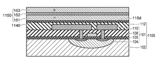
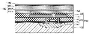
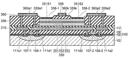
- FIG. 1 is a schematic cross-sectional view illustrating a part of the image display device according to the embodiment.
- FIG. 1 schematically shows the configuration of the sub-pixel 20 of the image display device of the present embodiment.
- the pixel 10 constituting the image displayed on the image display device is composed of a plurality of subpixels 20. In the following, it may be described using the three-dimensional coordinate system of XYZ.
- the subpixels 20 are arranged on a two-dimensional plane. Let the two-dimensional plane in which the subpixels 20 are arranged be the XY plane.
- the subpixels 20 are arranged along the X-axis direction and the Y-axis direction.
- the subpixel 20 has a light emitting surface 153S substantially parallel to the XY plane.
- the light emitting surface 153S mainly outputs light in the positive direction of the Z axis orthogonal to the XY plane.
- FIG. 1 schematically shows a cross section when the subpixel 20 is cut along a plane parallel to the XZ plane.
- This cross-sectional view is a cross-sectional view taken along the line AA'in FIG. 4, which will be described later.
- the subpixel 20 of the image display device includes a transistor 103, a first wiring layer 110, a first insulating film (interlayer insulating film) 112, a light emitting element 150, and a second insulation.
- a film (interlayer insulating film) 156, a second wiring layer 160, and a via 161d are provided.
- the subpixel 20 further includes a color filter 180.
- the color filter (wavelength conversion member) 180 is provided on the surface resin layer 170 via a transparent thin film adhesive layer 188.
- the surface resin layer 170 is provided on the light emitting element 150, the interlayer insulating film 156, and the wiring layer 160.
- the transistor 103 is formed on the substrate 102. As shown in FIGS. 3 and 12 described later, in addition to the transistor 103, circuit elements such as other transistors, resistors, and capacitors are formed on the substrate 102, and the circuit 101 is formed by wiring or the like. In the following, it is assumed that the circuit 101 includes an element forming region 104 in which a circuit element is formed, an insulating layer 105, a wiring layer 110, a via connecting the wiring layer 110 and the circuit element, and an insulating film 108 that insulates between the circuit elements. ..
- the circuit board 100 may include other components such as the substrate 102, the circuit 101, and the interlayer insulating film 112.
- the transistor 103 includes a p-type semiconductor region 104b, an n-type semiconductor region 104s and 104d, and a gate 107.
- the gate 107 is provided on the p-type semiconductor region 104b via the insulating layer 105.
- the insulating layer 105 is provided to insulate the element forming region 104 and the gate 107 and to sufficiently insulate the other adjacent circuit elements. When a voltage is applied to the gate 107, a channel can be formed in the p-type semiconductor region 104b.
- the transistor 103 is an n-channel MOSFET.
- the element forming region 104 is provided on the substrate 102.
- the substrate 102 is, for example, a Si substrate.
- the element forming region 104 includes a p-type semiconductor region 104b and an n-type semiconductor region 104s and 104d.
- the p-type semiconductor region 104b is provided near the surface of the substrate 102.
- the n-type semiconductor regions 104s and 104d are provided in the p-type semiconductor region 104b in the vicinity of the surface of the p-type semiconductor region 104b so as to be separated from each other.
- An insulating layer 105 is provided on the surface of the substrate 102.
- the insulating layer 105 also covers the element forming region 104, and also covers the surfaces of the p-type semiconductor region 104b and the n-type semiconductor regions 104s and 104d.
- the insulating layer 105 is, for example, SiO 2 .
- the insulating layer 105 may be a multi-layered insulating layer containing SiO 2 or Si 3 N 4 depending on the covering region.
- the insulating layer 105 may include a layer of an insulating material having a high dielectric constant.
- a gate 107 is provided on the p-type semiconductor region 104b via the insulating layer 105.
- the gate 107 is provided between the n-type semiconductor regions 104s and 104d.
- the gate 107 is, for example, polycrystalline Si.
- the gate 107 may contain silicide or the like having a resistance lower than that of polycrystalline Si.
- the gate 107 and the insulating layer 105 are covered with the insulating film 108.
- the insulating film 108 is, for example, SiO 2 or Si 3 N 4 or the like.
- an organic insulating film such as PSG (Phosphorus Silicon Glass) or BPSG (Boron Phosphorus Silicon Glass) may be further provided.
- a first wiring layer (first wiring layer) 110 is formed on the insulating film 108.
- the first wiring layer 110 includes a plurality of wirings having different potentials, and includes wirings 110s and 110d. As described above, in the cross-sectional views after FIG. 1, the code of the wiring layer is assumed to be displayed at a position next to one wiring included in the wiring layer.
- Vias 111s and 111d are provided between the wirings 110s and 110d of the wiring layer 110 and the n-type semiconductor regions 104s and 104d, respectively, and are electrically connected to each other.
- the wiring layer 110 and the vias 111s and 111d are formed of, for example, a metal such as Al or Cu.
- the wiring layer 110 and the vias 111s and 111d may contain a refractory metal or the like.
- a first interlayer insulating film 112 is further provided as a flattening film on the insulating film 108 and the wiring layer 110.
- the interlayer insulating film (first insulating film) 112 is, for example, an organic insulating film such as PSG or BPSG.
- the first interlayer insulating film 112 also functions as a protective film that protects the surface of the circuit board 100.
- a buffer layer 140 is provided over the interlayer insulating film 112.
- the buffer layer (buffer layer) 140 includes a nitride such as AlN. By providing the buffer layer 140, it can be expected to reduce crystal defects generated when the light emitting element 150 is epitaxially grown. As described above, the light emitting element 150 is directly provided on the first interlayer insulating film 112, not only when the buffer layer 140 is provided between the light emitting element 150 and the first interlayer insulating film 112. It may be.
- the wiring 110s in the circuit board 100 is provided so as to extend in the X-axis direction to the position where the light emitting element 150 is placed. As shown in FIG. 4, which will be described later, the wiring 110s extends in the Y-axis direction as long as or longer than the length of the light emitting element in the Y-axis direction.
- the outer circumference of the wiring 110s includes the outer circumference when the light emitting element 150 is projected from above the Z axis in the XY plan view.
- the wiring 110s can block the scattering of light downward from the light emitting element 150 so that it does not reach the transistor 103.
- the downward scattering of the light emitting element 150 can be reflected on the light emitting surface 153S side to improve the luminous efficiency.
- the wiring 110s blocks the scattered light below the light emitting element 150, the arrival of the light to the transistor 103 is suppressed, and the malfunction of the transistor 103 can be prevented.
- the light emitting element 150 includes an n-type semiconductor layer (first semiconductor layer) 151, a light emitting layer 152, and a p-type semiconductor layer (second semiconductor layer) 153.
- the n-type semiconductor layer 151, the light emitting layer 152, and the p-type semiconductor layer 153 are laminated in this order from the interlayer insulating film 112 of the circuit board 100 toward the positive direction of the Z axis, that is, toward the light emitting surface 153S.
- the light emitting element 150 has, for example, a substantially square or rectangular shape in XY plan view, but the corners may be rounded.
- the light emitting element 150 may have, for example, an elliptical shape or a circular shape in an XY plan view.
- the degree of freedom in layout is improved by appropriately selecting the shape and arrangement of the light emitting elements in a plan view.
- the n-type semiconductor layer 151 has a stepped portion 151a extending on the buffer layer 140 in the X-axis direction.
- the light emitting element 150 for example, a nitride semiconductor such as In X Al Y Ga 1-XY N (0 ⁇ X, 0 ⁇ Y, X + Y ⁇ 1) is preferably used.
- the light emitting element 150 is a so-called blue light emitting diode, and the wavelength of the light emitted by the light emitting element 150 is, for example, about 467 nm ⁇ 20 nm.
- the wavelength of the light emitted by the light emitting element 150 may be bluish purple emission of about 410 nm ⁇ 20 nm.
- the wavelength of the light emitted by the light emitting element 150 is not limited to the above-mentioned value, and may be appropriate.
- the second interlayer insulating film (second insulating film) 156 covers the buffer layer 140 and the light emitting element 150.
- the second interlayer insulating film 156 is formed of a transparent resin.
- the interlayer insulating film 156 also has a function of protecting the light emitting element 150 and flattening the surface due to the wiring layer 160 formed on the second interlayer insulating film 156.
- a via (second via) 161k is provided so as to penetrate the second interlayer insulating film 156.
- One end of the via 161k is connected to the step portion 151a.
- the via (first via) 161d is provided so as to penetrate the interlayer insulating films 112 and 156. One end of the via 161d is connected to the wiring 110d.
- the wiring layer 160 is provided on the flattened interlayer insulating film 156.
- the wiring layer 160 includes wirings 160a and 160k.
- the wiring 160a is connected to the p-type semiconductor layer 153 via a contact hole opened in the interlayer insulating film 156. Although not shown in this figure, the wiring 160a is connected to a power line that supplies power to the subpixel 20.
- the wiring 160k is connected to the other ends of the vias 161k and 161d. Therefore, the n-type semiconductor layer 151 of the light emitting element 150 is electrically connected to the main electrode of the transistor 103 via the vias 161k and 161d and the wirings 160k and 110d.
- the surface resin layer 170 covers the second interlayer insulating film 156 and the second wiring layer 160.
- the surface resin layer 170 is a transparent resin, protects the interlayer insulating film 156 and the wiring layer 160, and provides a flattening surface for adhering the color filter 180.
- the color filter 180 includes a light-shielding unit 181 and a color conversion unit 182.
- the color conversion unit 182 is provided directly above the light emitting surface 153S of the light emitting element 150 according to the shape of the light emitting surface 153S.
- the portion other than the color conversion unit 182 is a light-shielding unit 181.
- the light-shielding unit 181 is a so-called black matrix, which reduces bleeding due to color mixing of light emitted from the adjacent color conversion unit 182 and makes it possible to display a sharp image.
- the color conversion unit 182 has one layer or two layers.
- FIG. 1 shows a two-layer portion. Whether it is one layer or two layers is determined by the color of the light emitted by the subpixel 20, that is, the wavelength.
- the color conversion unit 182 preferably has two layers.
- the emission color of the subpixel 20 is blue, it is preferably one layer.
- the first layer closer to the light emitting element 150 is the color conversion layer 183
- the second layer is the filter layer 184. That is, the filter layer 184 is laminated on the color conversion layer 183.
- the color conversion layer 183 is a layer that converts the wavelength of the light emitted by the light emitting element 150 into a desired wavelength.
- the light having a wavelength of 467 nm ⁇ 20 nm of the light emitting element 150 is converted into light having a wavelength of, for example, about 630 nm ⁇ 20 nm.
- the light having a wavelength of 467 nm ⁇ 20 nm of the light emitting element 150 is converted into light having a wavelength of, for example, about 532 nm ⁇ 20 nm.
- the filter layer 184 blocks the wavelength component of blue light emission remaining without color conversion in the color conversion layer 183.
- the subpixel 20 may output the light through the color conversion layer 183, or outputs the light as it is without passing through the color conversion layer 183. You may do so.
- the wavelength of the light emitted by the light emitting element 150 is about 467 nm ⁇ 20 nm
- the subpixel 20 may output the light without passing through the color conversion layer 183.
- the wavelength of the light emitted by the light emitting element 150 is 410 nm ⁇ 20 nm, it is preferable to provide one color conversion layer 183 in order to convert the wavelength of the output light to about 467 nm ⁇ 20 nm.
- the subpixel 20 may have the filter layer 184.
- the filter layer 184 By providing the filter layer 184 on the blue subpixel 20, minute external light reflection generated on the surface of the light emitting element 150 is suppressed.
- FIGS. 2A and later are schematic cross-sectional views illustrating each modification of the image display device of the present embodiment.
- the display of the surface resin layer 170 and the color filter 180 is omitted in order to avoid complication.
- a surface resin layer and a color filter are provided on the second interlayer insulating film and the second wiring layer. The same applies to the cases of other embodiments and modifications thereof described later.
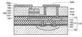
- the subpixels 20a and 20b have a configuration of the light emitting element 150a different from that of the first embodiment described above.
- the other components are the same as those in the first embodiment described above, and detailed description thereof will be omitted as appropriate.
- the subpixel 20a includes a light emitting element 150a.
- the light emitting element 150a is covered with a second interlayer insulating film (second insulating film) 256.
- the second interlayer insulating film 256 is preferably a white resin.
- the interlayer insulating film 256 as a white resin, the light emitting element 150a can reflect the light emitted in the lateral direction or the downward direction, and the brightness of the light emitting element 150a can be substantially improved.
- the second interlayer insulating film 256 may be a black resin.
- the interlayer insulating film 256 as a black resin, scattering of light in the subpixels is suppressed, and stray light is suppressed more effectively.
- An image display device in which stray light is suppressed can display a sharper image.
- the second interlayer insulating film 256 has an opening 158.
- the opening 158 is formed by removing a part of the interlayer insulating film 256 above the light emitting element 150a.
- the wiring 160a1 is connected to the p-type semiconductor layer 153a exposed by the opening 158.
- the p-type semiconductor layer 153a has a light emitting surface 153S exposed by the opening 158.
- the light emitting surface 153S is a surface of the p-type semiconductor layer 153a facing the surface in contact with the light emitting layer 152.
- the light emitting surface 153S is preferably roughened. When the light emitting surface 153S is a rough surface, the light emitting element 150a can improve the light extraction efficiency.
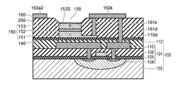
- transparent electrodes 159a and 159k are provided on the wirings 160a and 160k, respectively.
- the transparent electrode 159a is provided on the light emitting surface 153S of the opened p-type semiconductor layer 153a, and electrically connects the wiring 160a2 and the p-type semiconductor layer 153a.
- the connection area with the p-type semiconductor layer 153a can be increased, and the luminous efficiency can be improved.
- the connection area between the light emitting surface 153S and the transparent electrode 159a can be increased, and the contact resistance can be reduced.
- FIG. 2C shows a case where the circuit element such as the transistor 103 and the light emitting element 150 are arranged so as to be offset from each other on the XY plane.
- the light emitting element 150 and the transistor 130 may be arranged so as not to overlap each other in a plan view.
- a depletion layer region is generated between the p-type semiconductor region 104b and the n-type substrate 102, and this depletion layer region may function as a parasitic photodiode. It is preferable that the parasitic photodiode does not overlap with the light-irradiated region generated immediately below the light emitting element 150.
- the distance between the end portion when the light emitting layer 152 is projected onto the surface of the substrate 102 in XY plan view and the boundary of the p-type semiconductor region 104b is at least about 1 ⁇ m or more.
- the wiring 110s3 is not extended to the position where the light emitting element 150 is placed. That is, the wiring 110s3 does not necessarily include the outer peripheral portion of the light emitting element 150 when projected from above the Z axis in the XY plane view.
- the wiring 160k3 is extended longer in the X-axis direction than in the case of the above-described embodiment and other modifications.
- the light emitting element 150 when the light emitting element 150 is arranged sufficiently away from the circuit element, the scattered light in the negative direction of the Z axis is reduced, so that the circuit element such as the transistor 103 is less likely to malfunction due to the light. Become.
- the wiring in the circuit board 100 the wiring is not used for shading, so that the degree of freedom in circuit arrangement is improved and the integration density can be improved.
- any of the configurations of the subpixels 20 to 20c shown above can be included.
- FIG. 3 is a schematic block diagram illustrating an image display device according to the present embodiment.
- the image display device 1 of the present embodiment includes a display area 2.
- Subpixels 20 are arranged in the display area 2.
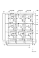
- the subpixels 20 are arranged in a grid pattern, for example. For example, n subpixels 20 are arranged along the X axis, and m subpixels 20 are arranged along the Y axis.
- Pixel 10 includes a plurality of subpixels 20 that emit light of different colors.
- the subpixel 20R emits red light.
- the subpixel 20G emits green light.
- the subpixel 20B emits blue light.
- the emission color and brightness of one pixel 10 are determined by the three types of sub-pixels 20R, 20G, and 20B emitting light with desired brightness.
- One pixel 10 includes three sub-pixels 20R, 20G, 20B, and the sub-pixels 20R, 20G, 20B are linearly arranged on the X-axis, for example, as in this example.
- subpixels of the same color may be arranged in the same column, or subpixels of different colors may be arranged for each column as in this example.
- the image display device 1 further includes a power supply line 3 and a ground line 4.
- the power line 3 and the ground line 4 are arranged in a grid pattern along the array of subpixels 20.
- the power supply line 3 and the ground line 4 are electrically connected to each subpixel 20, and power is supplied to each subpixel 20 from a DC power source connected between the power terminal 3a and the GND terminal 4a.
- the power supply terminal 3a and the GND terminal 4a are provided at the ends of the power supply line 3 and the ground line 4, respectively, and are connected to a DC power supply circuit provided outside the display area 2. A positive voltage is supplied to the power supply terminal 3a with reference to the GND terminal 4a.
- the image display device 1 further has a scanning line 6 and a signal line 8.
- the scanning line 6 is laid out in a direction parallel to the X axis. That is, the scanning lines 6 are laid out along the array in the row direction of the subpixels 20.
- the signal line 8 is laid out in a direction parallel to the Y axis. That is, the signal line 8 is laid out along the array of the subpixels 20 in the column direction.
- the image display device 1 further includes a row selection circuit 5 and a signal voltage output circuit 7.
- the row selection circuit 5 and the signal voltage output circuit 7 are provided along the outer edge of the display area 2.
- the row selection circuit 5 is provided along the Y-axis direction of the outer edge of the display area 2.
- the row selection circuit 5 is electrically connected to the subpixels 20 of each column via the scanning line 6 to supply a selection signal to each subpixel 20.
- the signal voltage output circuit 7 is provided along the outer edge of the display area 2.
- the signal voltage output circuit 7 is provided along the X-axis direction of the outer edge of the display area 2.
- the signal voltage output circuit 7 is electrically connected to the subpixel 20 of each line via the signal line 8 to supply a signal voltage to each subpixel 20.
- the subpixel 20 includes a light emitting element 22, a selection transistor 24, a drive transistor 26, and a capacitor 28.
- the selection transistor 24 may be displayed as T1
- the drive transistor 26 may be displayed as T2
- the capacitor 28 may be displayed as Cm.
- the light emitting element 22 is connected in series with the drive transistor 26.
- the drive transistor 26 is an n-channel MOSFET, and the cathode electrode, which is the n electrode of the light emitting element 22, is connected to the drain electrode, which is the main electrode of the drive transistor 26.
- the series circuit of the light emitting element 22 and the drive transistor 26 is connected between the power supply line 3 and the ground line 4.
- the drive transistor 26 corresponds to the transistor 103 in FIG. 1 and the like
- the light emitting element 22 corresponds to the light emitting element 150 in FIG. 1 and the like.
- the voltage applied between the gate and the source of the drive transistor 26 determines the current flowing through the light emitting element 22, and the light emitting element 22 emits light with a brightness corresponding to the current flowing through the light emitting element 22.
- the selection transistor 24 is connected between the gate electrode of the drive transistor 26 and the signal line 8 via a main electrode.
- the gate electrode of the selection transistor 24 is connected to the scanning line 6.
- a capacitor 28 is connected between the gate electrode of the drive transistor 26 and the ground wire 4.
- the row selection circuit 5 selects one row from the array of subpixels 20 in the m row and supplies the selection signal to the scanning line 6.
- the signal voltage output circuit 7 supplies a signal voltage having the required analog voltage value for each subpixel 20 in the selected row.
- a signal voltage is applied between the gate and source of the drive transistor 26 of the subpixel 20 in the selected row.
- the signal voltage is held by the capacitor 28.
- the drive transistor 26 causes a current corresponding to the signal voltage to flow through the light emitting element 22.
- the light emitting element 22 emits light with a brightness corresponding to the flowing current.
- the row selection circuit 5 sequentially switches the rows to be selected and supplies the selection signal. That is, the row selection circuit 5 scans the row in which the subpixels 20 are arranged. A current corresponding to the signal voltage flows through the light emitting element 22 of the subpixel 20 that is sequentially scanned to emit light. Each pixel 10 emits light with an emission color and brightness determined by the emission color and brightness of each of the RGB color subpixels 20, and an image is displayed in the display area 2.
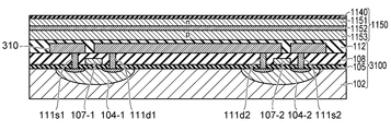
- FIG. 4 is a schematic plan view illustrating a part of the image display device of the present embodiment.
- the light emitting element 22 (150) and the drive transistor 26 (103) are laminated in the Z-axis direction, and the cathode electrode of the light emitting element 22 (150) is formed by the via 161d. Is electrically connected to the drain electrode of the drive transistor 26 (103).
- the plan view of the I layer is schematically displayed in the upper part of FIG. 4, and the plan view of the II layer is schematically displayed in the lower part.
- the first layer is referred to as “I” and the second layer is referred to as “II”.
- the I-th layer is a layer on which the light emitting element 22 (150) is formed. That is, in FIG. 1, the first layer includes layers from the buffer layer 140 to the second wiring layer 160 in the positive direction of the Z axis. In FIG. 4, the buffer layer 140 and the second interlayer insulating film 156 are not shown.
- the second layer includes the layers from the substrate 102 to the first interlayer insulating film 112 in the positive direction of the Z axis in FIG. In FIG. 4, the substrate 102, the insulating layer 105, the insulating film 108, and the first interlayer insulating film 112 are not shown. In this figure, the channel region 104c is shown as the element forming region 104.
- FIG. 1 is an arrow cross section of the AA'line at the location indicated by the alternate long and short dash line in each of the I layer and the II layer.
- a wiring 160k is connected to the n-type semiconductor layer 151 which is a cathode electrode of the light emitting element 150 via a via 161k (FIG. 1) and a contact hole 161k1 thereof.
- the wiring 160k is connected to one end of the via 161d via a contact hole 161d1 provided in the second interlayer insulating film 156.
- the via 161d is schematically shown by a chain double-dashed line in the figure.
- the other end of the via 161d is connected to the wiring 110d via the contact hole 161d2 provided in the first interlayer insulating film 112.
- the wiring 110d is connected to the via 111d (FIG. 1) via the contact hole 111c1 opened in the insulating film 108, and is connected to the drain electrode of the transistor 103.
- the light emitting element 150 and the transistor 103 formed in the first layer and the second layer, which are different layers, can be electrically connected by the via 161d penetrating the interlayer insulating films 156 and 112.
- the wiring 110s has a light-shielding portion 110s1.
- the light-shielding portion (part) 110s1 is a rectangular portion having a length L2 in the X-axis direction and a length W2 in the Y-axis direction.
- the light-shielding portion 110s1 is provided directly below the light-emitting element 150.
- the light emitting element 150 has a rectangular bottom surface having a length L1 in the X-axis direction and a length W1 in the Y-axis direction.
- the length of each part is set so that L2> L1 and W2> W1. Since the light-shielding portion 110s1 is provided directly below the light-emitting element 150, the outer circumference of the light-shielding portion 110s1 includes the outer circumference of the light-emitting element 150. The outer circumference of the light-shielding portion 110s1 may include the outer circumference of the light emitting element 150, and the shape of the light-shielding portion 110s1 is not limited to a square shape and can be any suitable shape.
- the light emitting element 150 emits light upward, and also emits light downward, and includes reflected light, scattered light, and the like at the interface between the interlayer insulating film 112 and the surface resin layer 170. Therefore, preferably, the outer circumference of the light-shielding portion 110s1 is set to include the outer circumference of the light emitting element 150 projected on the light-shielding portion 110s1 in the XY plan view. By setting the light-shielding portion 110s1 in this way, it is possible to suppress the arrival of light below the light emitting element 150 and reduce the influence of light on the circuit element.
- the manufacturing method of the image display device 1 of this embodiment will be described.
- 5A to 6C are schematic cross-sectional views illustrating the method of manufacturing the image display device of the present embodiment.
- the semiconductor growth substrate 1194 is prepared.
- the semiconductor growth substrate 1194 has a semiconductor layer 1150 grown on the crystal growth substrate (first substrate) 1001.
- the crystal growth substrate 1001 is, for example, a Si substrate, a sapphire substrate, or the like.
- a Si substrate is used.
- the buffer layer 1140 is formed on one surface of the crystal growth substrate 1001.
- nitride such as AlN is preferably used as the buffer layer (buffer layer) 1140.
- the buffer layer 1140 is used to alleviate the mismatch at the interface between the GaN crystal and the crystal growth substrate 1001 when epitaxially growing GaN.
- the n-type semiconductor layer 1151, the light emitting layer 1152, and the p-type semiconductor layer 1153 are laminated on the buffer layer 1140 in this order from the buffer layer 1140 side.
- a vapor phase growth method (Chemical Vapor Deposition, CVD method) is used, and an organic metal vapor deposition method (Metal Organic Chemical Vapor Deposition, MOCVD method) is preferably used.
- the semiconductor layer 1150 is, for example, In X Al Y Ga 1-XY N (0 ⁇ X, 0 ⁇ Y, X + Y ⁇ 1) or the like.
- the support substrate 1190 is adhered to the open surface of the p-type semiconductor layer 1153 on the side facing the side on which the crystal growth substrate 1001 is provided.
- the support substrate 1190 is made of, for example, Si or quartz.
- the crystal growth substrate 1001 is removed. For example, a laser is used to remove the crystal growth substrate 1001.
- the circuit board 1100 is prepared.
- the circuit board (second board) 1100 has a circuit 101 described with reference to FIG. 1 and the like for the configuration of the subpixel 20.
- one surface of the circuit board 1100 and the surface of the buffer layer 1140 of the semiconductor layer 1150 are aligned, and both are bonded together.
- the bonded surface of the circuit board 1100 is an exposed surface of the interlayer insulating film 112 formed on the wiring layer 160.
- a low melting point metal or a low melting point alloy may be used for heat crimping.
- the low melting point metal is, for example, Sn, In, or the like, and the low melting point alloy can be, for example, an alloy containing Zn, In, Ga, Sn, Bi, or the like as a main component.
- the bonded surfaces of each substrate are flattened using chemical mechanical polishing (CMP), etc., and then the bonded surfaces are cleaned and adhered in vacuum by plasma treatment. You may let it.
- CMP chemical mechanical polishing
- the semiconductor layer 1150 may be attached to the support substrate 1190, the crystal growth substrate 1001 may be removed, and then the buffer layer 1140 may also be removed.
- the surface of the n-type semiconductor layer 1151 opened by removing the buffer layer 1140 is bonded to the circuit board 1100.
- a semiconductor growth substrate in which the semiconductor layer 1150 is crystal-grown may be used without providing the buffer layer 1140.
- the circuit board 1100 is bonded to the semiconductor layer 1150 via the buffer layer 1140 by wafer bonding.
- the semiconductor layer 1150 is formed in the shape of the light emitting element 150.
- a dry etching process is used, and preferably anisotropic plasma etching (Reactive Ion Etching, RIE) is used.
- an interlayer insulating film is formed so as to cover the light emitting element 150.
- Via holes are formed in the interlayer insulating film. After that, the via hole is filled with a conductive metal material. Either wet etching or dry etching can be used to form the via holes.
- a conductive layer is formed in the via hole by sputtering or the like, and a wiring layer 160 is formed by photolithography. After forming the via hole, the via and the wiring layer may be formed at the same time.
- a part of the circuit other than the subpixel 20 is formed in the circuit board 100.
- the row selection circuit 5 (FIG. 3) can be formed in the circuit board 100 together with the drive transistor, the selection transistor, and the like. That is, the row selection circuit 5 may be incorporated at the same time by the manufacturing process described above.
- the signal voltage output circuit 7 is mounted on another board together with the CPU and other circuit elements, and is mutually connected with the wiring of the circuit board 100, for example, before incorporating the color filter described later or after incorporating the color filter. Connected to.
- the circuit board 1100 is a wafer containing the circuit 101.
- the circuit board 1100 is formed with circuits 101 for one or more image display devices.
- the circuit 101 for forming one image display device is divided into a plurality of circuit boards 1100 and formed, and all of the divided circuits are combined to form 1 One image display device may be configured.
- the crystal growth substrate 1001 is a wafer having the same size as the wafer-shaped circuit board 1100.
- the semiconductor layers 1150 formed on the plurality of crystal growth substrates 1001 may be bonded to one circuit board 1100.
- FIGS. 7A and 7B are schematic cross-sectional views illustrating a manufacturing method of a modified example of the image display device of the present embodiment.
- 7A and 7B show the manufacturing process for forming the subpixel 20a of FIG. 2A.
- the same steps as in the case of the first embodiment are performed until the second interlayer insulating film 256 (156) is formed.
- FIGS. 7A and 7B are executed after the step of FIG. 6B or FIG. 6C.
- the second interlayer insulating film 256 is etched to form an opening 158 to expose the surface of the p-type semiconductor layer 153.
- the etching may be wet etching or dry etching.
- the light emitting surface 153S of the exposed p-type semiconductor layer 153 is roughened in order to improve the luminous efficiency.
- each wiring 160a1,160k is formed by photolithography.
- the wiring 160a1 is formed so as to be connected to the light emitting surface 153S of the exposed p-type semiconductor layer 153.
- the subpixel 20a of the modified example is formed.
- 8A and 8B are schematic cross-sectional views illustrating a manufacturing method of one modification of the image display device of the present embodiment.
- 8A and 8B show the manufacturing process for forming the subpixel 20b of FIG. 2B.
- the same steps as in the case of the above-mentioned modified example are obtained until the opening 158 is formed. Therefore, in the following description, it is assumed that the steps of FIGS. 8A and 8B are executed after FIG. 7A.
- each wiring 160a2, 160k is formed.
- the wiring 160a2 is not connected to the light emitting surface 153S of the p-type semiconductor layer 153.
- a transparent conductive film covering the wiring layer 160, the second interlayer insulating film 256 (156), and the light emitting surface 153S of the p-type semiconductor layer 153 is formed.
- the transparent conductive film an ITO film, a ZnO film, or the like is preferably used.
- the required transparent electrodes 159a, 159k are formed by photolithography.
- the transparent electrode 159a is formed on the wiring 160a2 and also on the light emitting surface 153S of the p-type semiconductor layer 153. Therefore, the wiring 160a2 and the p-type semiconductor layer 153 are electrically connected.
- the transparent electrode 159a is provided so as to cover the entire surface of the exposed light emitting surface 153S and is connected to the light emitting surface 153S.
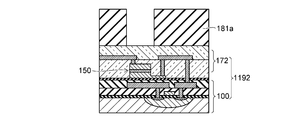
- FIG. 9 is a schematic cross-sectional view illustrating the method for manufacturing the image display device of the present embodiment.
- the wiring and the like in the circuit board 100 and the interlayer insulating films 112 and 156 are not shown. Further, in FIG. 9, a part of the color conversion member such as the color filter 180 is displayed.
- a structure including a buffer layer 140, a light emitting element 150, vias 161k, 161d, a wiring layer 160, an interlayer insulating film 156, and a surface resin layer 170 is referred to as a light emitting circuit unit 172.
- a structure in which the light emitting circuit unit 172 is provided on the circuit board 100 is referred to as a structure 1192.
- the color filter 180 is adhered to the structure 1192 on one side.
- the other surface of the color filter 180 is adhered to the glass substrate 186.
- a transparent thin film adhesive layer 188 is provided on one surface of the color filter 180, and is adhered to the surface of the structure 1192 on the light emitting circuit portion 172 side via the transparent thin film adhesive layer 188.
- the color filter 180 has color conversion units arranged in the positive direction of the X-axis in the order of red, green, and blue.
- a red color conversion layer 183R and a green color conversion layer 183G are provided on the first layer, and a filter layer 184 is provided on the second layer, respectively.
- a single-layer color conversion layer 183B is provided for blue.
- a light-shielding unit 181 is provided between the color conversion units.
- the color filter 180 is attached to the structure 1192 by aligning the positions of the color conversion layers 183R, 183G, and 183B of each color with the positions of the light emitting element 150.
- 10A to 10D are schematic cross-sectional views showing a manufacturing method of a modified example of the image display device of the present embodiment.
- 10A-10D show a method of forming a color filter by an inkjet.
- a structure 1192 having a light emitting circuit unit 172 attached to the circuit board 100 is prepared.
- a light-shielding portion 181a is formed on the structure 1192.
- the light-shielding portion 181a is formed by using, for example, screen printing, photolithography technology, or the like.
- the phosphor 183a corresponding to the emission color is ejected from the inkjet nozzle.
- the phosphor 183a colors the region where the light-shielding portion 181a is not formed.
- a fluorescent paint using a general phosphor material or a quantum dot phosphor material is used as the phosphor 183a.
- a quantum dot phosphor material it is preferable because each emission color can be realized, monochromaticity is high, and color reproducibility can be high.
- the drying process is performed at an appropriate temperature and time. The thickness of the coating film at the time of coloring is set to be thinner than the thickness of the light-shielding portion 181a.
- the blue light emitting subpixel may not form a color conversion part, so that the phosphor is not ejected.
- the color conversion unit may be one layer, so that the thickness of the coating film of the blue phosphor is preferably set to that of the light shielding portion 181a. It is about the same as the thickness.
- the paint 184a for the filter layer is ejected from the inkjet nozzle.
- the paint 184a is applied over the coating film of the phosphor 183a.
- the total thickness of the coating film of the phosphor 183a and the coating film 184a is about the same as the thickness of the light-shielding portion 181a.
- the image display device 1 can be manufactured.
- the semiconductor layer 1150 including the light emitting layer 1152 for the light emitting element 150 is mounted on the circuit board 1100 (100) including the circuit elements such as the transistor 103 for driving the light emitting element 150. to paste together. Then, the semiconductor layer 1150 is etched to form the light emitting element 150. Therefore, the step of transferring the light emitting element can be remarkably shortened as compared with the case of individually transferring the light emitting element separated into the circuit board 1100 (100).
- the number of subpixels exceeds 24 million, and in the case of an 8K image quality image display device, the number of subpixels exceeds 99 million. It would take an enormous amount of time to mount such a large number of light emitting elements individually on a circuit board, and it is difficult to realize an image display device using micro LEDs at a realistic cost. Further, if a large number of light emitting elements are individually mounted, the yield is reduced due to poor connection at the time of mounting, and further cost increase is unavoidable.
- the entire semiconductor layer 1150 is attached to the circuit board 1100 (100) before the semiconductor layer 1150 is fragmented, so that the transfer step is performed once. Complete with.
- the light emitting element is directly formed on the circuit board by etching or the like, the light emitting element and the circuit element in the circuit board 1100 (100) are electrically connected by via formation, so that a uniform connection structure is realized. It is possible to suppress a decrease in yield.
- the semiconductor layer 1150 is attached to the circuit board 1100 (100) at the wafer level without being fragmented in advance or forming an electrode at a position corresponding to the circuit element, it is not necessary to perform alignment. Therefore, the pasting process can be easily performed in a short time. Since it is not necessary to align the light emitting element 150 at the time of pasting, the light emitting element 150 can be easily miniaturized, which is suitable for a high-definition display.
- FIG. 11 is a schematic cross-sectional view illustrating a part of the image display device according to the present embodiment.
- the configuration of the light emitting element 250 and the configuration of the transistor 203 for driving the light emitting element 250 are different from those of the other embodiments described above.
- the same components as in the case of the other embodiments described above are designated by the same reference numerals, and detailed description thereof will be omitted as appropriate.
- the subpixel 220 of the image display device of the present embodiment includes the transistor 203 and the light emitting element 250.
- the transistor 203 is formed in the element forming region 204 formed on the substrate 102.
- the element forming region 204 includes an n-type semiconductor region 204b and a p-type semiconductor region 204s and 204d.
- the n-type semiconductor region 204b is provided near the surface of the substrate 102.
- the p-type semiconductor regions 204s and 204d are provided in the n-type semiconductor region 204b in the vicinity of the surface of the n-type semiconductor region 204b so as to be separated from each other.
- a gate 107 is provided on the n-type semiconductor region 204b via the insulating layer 105.
- the gate 107 is provided between the p-type semiconductor regions 204s and 204d.
- the transistor 203 is a p-channel MOSFET.
- the light emitting element 250 includes a p-type semiconductor layer (first semiconductor layer) 253, a light emitting layer 252, and an n-type semiconductor layer (second semiconductor layer) 251.
- the p-type semiconductor layer 253, the light emitting layer 252, and the n-type semiconductor layer 251 are laminated in this order from the first interlayer insulating film 112 of the circuit board 100 toward the light emitting surface 251S.
- the light emitting element 250 has, for example, a substantially square or rectangular shape in XY plan view, but the corners may be rounded.
- the light emitting element 250 may have, for example, an elliptical shape or a circular shape in an XY plan view.
- the degree of freedom in layout is improved by appropriately selecting the shape and arrangement of the light emitting elements in a plan view.
- the p-type semiconductor layer 253 has a stepped portion 253a extending in the X-axis direction on the first interlayer insulating film 112.
- the light emitting element 250 may be made of the same material as in the other embodiments described above.
- the light emitting element 250 emits, for example, blue light having a wavelength of about 467 nm ⁇ 20 nm or blue-purple light having a wavelength of 410 nm ⁇ 20 nm.
- the light emitting element 250 is provided on the interlayer insulating film (first insulating film) 112 without interposing the buffer layer.
- the second interlayer insulating film (second insulating film) 256 covers the first interlayer insulating film 112 and the light emitting element 250.
- the second interlayer insulating film 256 has an opening 258.
- the opening 258 is formed on the light emitting element 250, and the interlayer insulating film 256 is not provided on the light emitting surface 251S of the light emitting element 250.
- a white resin is preferably used so that the light emitting element 250 reflects the light emitted and is effectively output from the opening 258.
- the light emitting surface 251S is a surface of the n-type semiconductor layer 251 facing the surface in contact with the light emitting layer 252.
- the light emitting surface 251S is roughened.
- a via (second via) 261a is provided so as to penetrate the interlayer insulating film 256.
- One end of the via 261a is connected to the step portion 253a.
- the via (first via) 161d is provided so as to penetrate the interlayer insulating films 112 and 256. One end of the via 161d is connected to the wiring 110d.
- the wiring layer 260 is provided on the interlayer insulating film 256.
- the wiring layer 260 includes wirings 260k and 260a.
- the wiring 260a is connected to the other ends of the vias 261a and 161d. Therefore, the p-type semiconductor layer 253 of the light emitting element 250 is electrically connected to the main electrode of the transistor 203 via the vias 261a and 161d.
- Wiring 260k is not shown, but is connected to the ground wire.
- a transparent electrode 259k is provided on the wiring 260k.
- the transparent electrode 259k extends to the light emitting surface 251S and is provided over the entire surface of the light emitting surface 251S. Therefore, the n-type semiconductor layer 251 is connected to the ground wire via the transparent electrode 259k and the wiring 260k.
- a transparent electrode 259a is also arranged on the wiring 260a.
- a surface resin layer 170 is provided on the interlayer insulating film 256 and the transparent electrodes 259k and 259a.
- FIG. 12 is a schematic block diagram illustrating an image display device according to the present embodiment.
- the image display device 201 of the present embodiment includes a display area 2, a row selection circuit 205, and a signal voltage output circuit 207.
- the sub-pixels 220 are arranged in a grid pattern as in the case of the other embodiments described above.
- the light emitting element 222 is provided on the ground wire 4, and the drive transistor 226 connected in series with the light emitting element 222 is provided on the power supply line 3. That is, the drive transistor 226 is connected to the higher potential side than the light emitting element 222.
- the drive transistor 226 is a p-channel MOSFET.
- a selection transistor 224 is connected between the gate electrode of the drive transistor 226 and the signal line 208.
- the capacitor 228 is connected between the gate electrode of the drive transistor 226 and the power supply line 3.
- the row selection circuit 205 and the signal voltage output circuit 207 perform selection signals and signal voltages having different polarities from those of the other embodiments described above in order to drive the drive transistor 226, which is a p-channel MOSFET, in scanning lines 206 and signal lines 208. Supply to.
- the row selection circuit 205 supplies a selection signal to the scanning line 206 so as to sequentially select one row from the array of m rows of subpixels 220.
- the signal voltage output circuit 207 supplies a signal voltage having the required analog voltage value to each subpixel 220 in the selected row.
- the drive transistor 226 of the subpixel 220 in the selected row causes a current corresponding to the signal voltage to flow through the light emitting element 222.
- the light emitting element 222 emits light with a brightness corresponding to the flowing current.
- FIG. 13A to 14B are schematic cross-sectional views illustrating the method of manufacturing the image display device of the present embodiment.
- the semiconductor growth substrate 1194 already described in FIG. 5A is used.
- the subsequent steps of preparing the semiconductor growth substrate 1194 having the semiconductor layer 1150 epitaxially grown via the buffer layer 1140 on the crystal growth substrate 1001 will be described.
- the semiconductor growth substrate 1194 is turned upside down and attached to the circuit board 1100 without removing the crystal growth substrate 1001 from the semiconductor growth substrate 1194. That is, the exposed surface of the p-type semiconductor layer 1153 on the opposite side of the crystal growth substrate 1001 is attached to the flattened surface of the interlayer insulating film 112 of the circuit board 1100 by wafer bonding as shown by the arrows in the figure. wear. Wafer bonding can be performed in the same manner as in the other embodiments described above.
- the crystal growth substrate 1001 is removed by laser irradiation or the like.
- the semiconductor layer 1150 is etched together with the buffer layer 1140 to form the light emitting element 250. Since the buffer layer 240 remains on the light emitting element 250, the buffer layer 240 is removed by further etching. The buffer layer 240 may be removed before forming the light emitting element 250.
- the first interlayer insulating film 112 and the second interlayer insulating film 256 covering the light emitting element 250 are formed. After that, a via hole is formed so as to penetrate the second interlayer insulating film 256. The via hole is filled with a conductive metal material.
- An opening 258 is formed in the second interlayer insulating film 256 to expose the light emitting surface 251S of the n-type semiconductor layer 251.
- the opening 258 is formed by either a wet or dry etching method.
- the light emitting surface 251S of the exposed n-type semiconductor layer 251 is roughened in order to improve the luminous efficiency.
- a wiring layer including the opening 258 is formed, and each wiring 260k and 260a is formed by photolithography.
- the wiring 260a is connected to the vias 261a and 161d.
- the wiring 260k is connected to a ground wire (not shown).
- transparent electrodes 259a and 259k are provided on the wirings 260a and 260k, respectively.
- the transparent electrode 259k is provided so as to extend to the light emitting surface 251S.
- the transparent electrode 259k is provided over the entire surface of the light emitting surface 251S. Therefore, the n-type semiconductor layer 251 is connected to the ground wire 4 via the transparent electrode 259k and the wiring 260k.
- FIG. 15 is a schematic cross-sectional view illustrating a part of a modified example of the image display device of the present embodiment. As shown in FIG. 15, in this modification, the wiring and the light emitting surface are electrically connected without using the transparent electrode. In the subpixel 220a, the wiring 260k1 is patterned so as to be directly connected to the n-type semiconductor layer 251 without a transparent electrode.
- the transparent interlayer insulating film is not roughened. It may be made to emit light via 156.
- This embodiment also has the same effect as that of the other embodiments described above. That is, since the semiconductor layer 1150 is bonded to the circuit board 1100 and then the individual light emitting elements 250 are formed by etching, the transfer process of the light emitting elements can be significantly shortened.
- the n-type semiconductor layer 251 as the light emitting surface 251S, the surface can be roughened more easily, and the wiring 260k1 is connected to the light emitting surface 251S.
- the wiring 260k1 is connected to the light emitting surface 251S.
- FIG. 16 is a schematic cross-sectional view illustrating a part of the image display device according to the present embodiment. As shown in FIG. 16, the image display device includes a subpixel group 320.
- the subpixel group 320 includes transistors 103-1 and 103-2, a first wiring layer 310, a first interlayer insulating film 112, a semiconductor layer 350, a second interlayer insulating film 356, and a second interlayer insulating film.
- the wiring layer 360 and vias 361d1 and 361d2 are included.
- the semiconductor layer 350 includes two light emitting surfaces 351S1 and 351S2, and the subpixel group 320 contains substantially two subpixels.
- the display area is formed by arranging the subpixel group 320 including substantially two subpixels in a grid pattern.
- Transistors 103-1 and 103-2 are formed in the element forming regions 104-1 and 104-2, respectively.
- the element forming regions 104-1 and 104-2 are n-type semiconductor layers, and p-type semiconductor layers are formed separated from the n-type semiconductor layers.
- the n-type semiconductor layer includes a channel region, and the p-type semiconductor layer includes a source region and a drain region, respectively.
- An insulating layer 105 is formed on the element forming regions 104-1 and 104-2, and gates 107-1 and 107-2 are formed via the insulating layer 105, respectively.
- Gates 107-1 and 107-2 are gates of transistors 103-1 and 103-2.
- the transistors 103-1 and 103-2 are p-channel MOSFETs.
- the insulating film 108 covers the two transistors 103-1 and 103-2.
- a wiring layer (first wiring layer) 310 is formed on the insulating film 108.
- Vias 111s1 and 111d1 are provided between the p-type semiconductor layer of the transistor (first transistor) 103-1 and the wiring layer 310, respectively. Vias 111s2 and 111d2 are provided between the p-type semiconductor layer of the transistor (second transistor) 103-2 and the wiring layer 310.
- the first wiring layer 310 includes wiring 310s, 310d1, 310d2.
- the wiring 310s is electrically connected to the p-type semiconductor layer corresponding to the source electrodes of the transistors 103-1 and 103-2 via the vias 111s1 and 111s2.
- Wiring 310s is not shown, but is connected to a power line.
- the wiring 310d1 is connected to the p-type semiconductor layer corresponding to the drain electrode of the transistor 103-1 via the via 111d1.
- the wiring 310d2 is connected to the drain electrode of the transistor 103-2 via the via 111d2.
- the first interlayer insulating film (first insulating film) 112 covers the transistors 103-1 and 103-2 and the wiring layer 310.
- the semiconductor layer 350 is provided above the interlayer insulating film 112.
- the single semiconductor layer 350 is provided between two driving transistors 103-1 and 103-2 arranged along the X-axis direction.
- the semiconductor layer 350 includes a p-type semiconductor layer (first semiconductor layer) 353, a light emitting layer 352, and an n-type semiconductor layer (second semiconductor layer) 351.
- the semiconductor layer 350 is laminated in the order of the p-type semiconductor layer 353, the light emitting layer 352, and the n-type semiconductor layer 351 from the side of the interlayer insulating film 112 toward the light emitting surfaces 351S1 and 351S2.
- the p-type semiconductor layer 353 has stepped portions 353a1 and 353a2.
- the step portion 353a1 is provided on the side of the transistor 103-1 and the step portion 353a2 is provided on the side of the transistor 103-2.
- the second interlayer insulating film (second insulating film) 356 covers the first interlayer insulating film 112 and the semiconductor layer 350.
- the interlayer insulating film 356 covers a part of the semiconductor layer 350.
- the interlayer insulating film 356 covers the surface of the n-type semiconductor layer 351 except for the light emitting surfaces (exposed surfaces) 351S1 and 351S2 of the semiconductor layer 350.
- the interlayer insulating film 356 covers the side surface of the semiconductor layer 350 and the stepped portions 353a1 and 353a2.
- the interlayer insulating film 356 is preferably a white resin.
- the transparent electrode 359k covers the portion of the semiconductor layer 350 that is not covered with the interlayer insulating film 356.
- the transparent electrode 359k is provided on the light emitting surfaces 351S1 and 351S2 of the n-type semiconductor layer 351 exposed from the openings 358-1 and 358-2 of the interlayer insulating film 356, respectively.
- the transparent electrode 359k is electrically connected to the n-type semiconductor layer 351.
- the vias 361a1 and 361a2 are provided so as to penetrate the interlayer insulating film 356. One ends of the vias 361a1 and 361a2 are connected to the stepped portions 353a1 and 353a2, respectively.
- the vias 361d1 and 361d2 are provided so as to penetrate the interlayer insulating films 356 and 112. One end of the vias 361d1 and 361d2 is connected to the wirings 310d1 and 310d2, respectively.
- the second wiring layer (second wiring layer) 360 is provided on the interlayer insulating film 356.
- the wiring layer 360 includes wirings 360a1 and 360a2.
- the via (first via) 361d1 is provided between the wiring (first wiring) 310d1 and the wiring (second wiring) 360a1.
- the via (second via) 361d2 is provided between the wiring (third wiring) 310d2 and the wiring (fourth wiring) 360a2.
- the wiring 360a1 is connected to the p-type semiconductor layer 353 via the via 361a1.
- the wiring 360a2 is connected to the p-type semiconductor layer 353 via the via 361a2. Therefore, the p-type semiconductor layer 353 is connected to the drain electrode of the transistor 103-1 via the wiring 360a1, the via 361d1, and the wiring 310d1.
- the p-type semiconductor layer 353 is connected to the drain electrode of the transistor 103-2 via the wiring 360a2, the via 361d2, and the wiring 310d2.
- the wiring layer 360 includes the wiring 360k.
- a transparent electrode 359k is provided on the wiring 360k, and the wiring 360k and the transparent electrode 359k are electrically connected to each other.
- the transparent electrode 359k is extended to openings 358-1, 358-2.
- the transparent electrodes 359k are provided over the entire surface of the light emitting surfaces 351S1 and 351S2 exposed from the openings 358-1 and 358-2, respectively, and are electrically connected to each other.
- Transparent electrodes 359a1 and 359a2 are also provided on the wirings 360a1 and 360a2, respectively, and are electrically connected to each other.
- the opening 358-1 is provided between the wirings 360a and 360k.
- the opening 358-2 is provided between the wirings 360k and 360a2.
- the wiring 360k is provided between the openings 358-1 and 358-2 in this example.
- the openings 358-1 and 358-2 are, for example, square or rectangular in XY plan view.
- the shape is not limited to a square, and may be a polygon such as a circle, an ellipse, or a hexagon.
- the light emitting surfaces 351S1 and 351S2 are also squares, rectangles, other polygons, circles, etc. in XY plan view.
- the shapes of the light emitting surfaces 351S1 and 351S2 may be similar to or different from the shapes of the openings 358-1 and 358-2.
- the transparent electrodes 359k are connected to the light emitting surfaces 351S1 and 351S2 exposed from the openings 358-1 and 358-2, respectively. Therefore, the electrons supplied from the transparent electrode 359k are injected into the n-type semiconductor layer 351 from the exposed light emitting surfaces 351S1 and 351S2.
- holes are injected into the p-type semiconductor layer 353 from the transistor 103-1 via the wiring 360a1, the via 361d1 and the wiring 310d1. Further, holes are injected into the p-type semiconductor layer 353 from the transistor 103-2 via the wiring 360a2, the via 361d2, and the wiring 310d2.
- Transistors 103-1 and 103-2 are driving transistors of adjacent subpixels, and are driven sequentially. Therefore, the holes injected from either one of the two transistors 103-1 and 103-2 are injected into the light emitting layer 352, and the electrons injected from the wiring 360k are injected into the light emitting layer 352 to emit light.
- the opening 358-1 is provided between the wiring 360k and the wiring 360a1, when the transistor 103-1 is turned on, light is emitted from the light emitting surface 351S1 exposed from the opening 358-1.
- the opening 358-2 is provided between the wiring 360k and the wiring 360a2, when the transistor 103-2 is turned on, light is emitted from the light emitting surface 351S2 exposed from the opening 358-2.
- 17A to 18B are schematic cross-sectional views illustrating the method of manufacturing the image display device of the embodiment.
- the semiconductor growth substrate 1194 including the crystal growth substrate 1001 in which the semiconductor layer 1150 is epitaxially grown is bonded to the circuit board 3100 by wafer bonding.
- the semiconductor layer 1150 and the like on the crystal growth substrate 1001 are the same as those already described in the case of the other embodiments described above, and detailed description thereof will be omitted.
- the circuit board 3100 is also the same as the structure already described in most of the other parts, although the circuit configuration is different from that of the other embodiments described above. In the following, only the reference numerals will be replaced and detailed description will be omitted as appropriate.
- the surface of the semiconductor layer 1150 opposite to the surface of the crystal growth substrate 1001 is joined to the flat surface of the interlayer insulating film 112 of the circuit board 3100. That is, the exposed surface of the p-type semiconductor layer 1153 of the semiconductor layer 1150 is bonded to the interlayer insulating film 112.
- the semiconductor layer 1150 is etched to form an end portion of the p-type semiconductor layer 353.
- Stepped portions 353a1 and 353a2 for connecting vias are formed at the ends of the p-type semiconductor layer 353.
- a light emitting layer 352 and an n-type semiconductor layer 351 are formed on the p-type semiconductor layer 353 other than the stepped portion.
- the interlayer insulating film 356 and the interlayer insulating film covering the semiconductor layer 350 are formed, and vias are formed. Further, a wiring layer 360 is formed, and wirings 360a1, 360k and the like are formed by etching.
- openings 358-1 and 358-2 are formed in the portion between the wirings 360a and 360k and the portion between the wirings 360a and 360k, respectively.
- the light emitting surfaces 351S1 and 351S2 of the n-type semiconductor layer exposed by the openings 358-1 and 358-2 are roughened, respectively.
- transparent electrodes 359a1,359a2,359k are formed.
- two light emitting surfaces 351S1 and 351S2 are provided on one semiconductor layer 350, but the number of light emitting surfaces is not limited to two, and three or more light emitting surfaces are one semiconductor. It can also be provided on the layer 350. As an example, one row or two rows of subpixels may be realized by a single semiconductor layer 350. As a result, as will be described later, it is possible to reduce the recombination current that does not contribute to light emission per light emitting surface and increase the effect of realizing a finer light emitting element.
- FIG. 19 is a schematic cross-sectional view illustrating a part of a modified example of the image display device according to the present embodiment.
- This modification is different from the case of the third embodiment described above in that two n-type semiconductor layers 3351a1 and 3351a2 are provided on the light emitting layer 352. In other respects, it is the same as in the third embodiment.
- the image display device of this modification includes a subpixel group 320a.
- the subpixel group 320a includes a semiconductor layer 350a.
- the semiconductor layer 350a includes a p-type semiconductor layer 353, a light emitting layer 352, and n-type semiconductor layers 3351a1, 3351a2.
- the p-type semiconductor layer 353, the light emitting layer 352, and the n-type semiconductor layers 3351a1, 3351a2 are laminated in this order from the interlayer insulating film 356 toward the light emitting surface 3351S1, 3351S2.
- the n-type semiconductor layers 3351a1 and 3351a2 are arranged on the light emitting layer 352 so as to be separated from each other along the X-axis direction.
- An interlayer insulating film 356 is provided between the n-type semiconductor layers 3351a1 and 3351a2, and the n-type semiconductor layers 3351a1 and 3351a2 are separated by an interlayer insulating film 356.
- a wiring 360k is provided on the interlayer insulating film 356.
- the n-type semiconductor layers 3351a1 and 3351a2 have substantially the same shape in XY plan view, and the shape is substantially square or rectangular, and may be another polygonal shape, circular shape, or the like.
- the n-type semiconductor layers 3351a1 and 3351a2 have light emitting surfaces 3351S1 and 3351S2, respectively.
- the light emitting surfaces 3351S1 and 3351S2 are surfaces of the n-type semiconductor layers 3351a1 and 3351a2 exposed by the openings 358-1 and 358-2, respectively.
- the shapes of the light emitting surfaces 3351S1 and 3351S2 in the XY plan view have substantially the same shape as the shape of the light emitting surface in the case of the third embodiment, and have a shape such as a square.
- the shape of the light emitting surfaces 3351S1 and 3351S2 is not limited to the square as in this embodiment, and may be a polygon such as a circle, an ellipse, or a hexagon.
- the shapes of the light emitting surfaces 3351S1 and 3351S2 may be similar to or different from the shapes of the openings 358-1 and 358-2.
- a transparent electrode 359k is provided on the light emitting surface 3351S1.
- a transparent electrode 359k is also provided on the light emitting surface 3351S2.
- the transparent electrode 359k is also provided on the wiring 360k, and the n-type semiconductor layers 3351a1, 3351a2 are connected to the wiring 360k via the transparent electrodes 359k connected to the light emitting surfaces 3351S1 and 3351S2.
- the wiring 360k is not shown, but is connected to a GND line.
- 20A and 20B are schematic cross-sectional views illustrating a method of manufacturing an image display device of this modified example.
- the same steps as those described in FIGS. 17A to 18A are adopted in the case of the third embodiment until the semiconductor layer 1150 is formed. The subsequent steps will be described below.
- the buffer layer 1140, the n-type semiconductor layer 1151, the light emitting layer 1152 and the p-type semiconductor layer 1153 are etched to form the light emitting layer 352 and the p-type semiconductor layer 353, and then the light emitting layer 352 and the p-type semiconductor layer 353 are formed. Further, two n-type semiconductor layers 3351a1 and 3351a2 are formed by etching. The buffer layer 340a on the two n-type semiconductor layers 3351a1 and 3351a2 is subsequently removed. The buffer layer 340a may be removed before etching the n-type semiconductor layers 3351a1 and 3351a2, depending on the situation of the manufacturing process to be used.
- the n-type semiconductor layers 3351a1 and 3351a2 may be formed by deeper etching. For example, etching for forming the n-type semiconductor layers 3351a1 and 3351a2 may be performed until the depth in the light emitting layer 352 or the p-type semiconductor layer 353 is reached. When the n-type semiconductor layer is deeply etched in this way, it is desirable that the etching position of the n-type semiconductor layer 351 is 1 ⁇ m or more away from the light emitting surfaces 3351S1 and 3351S2 of the n-type semiconductor layer described later. By separating the etching position from the light emitting surfaces 3351S1 and 3351S2, the recombination current can be suppressed.
- an interlayer insulating film 112 and an interlayer insulating film covering the semiconductor layer 3350a are formed, and then vias are formed. Further, a wiring layer 360 is formed, and wirings 360a1, 360k and the like are formed by etching.
- Apertures 358-1 and 358-2 are formed in the interlayer insulating film, respectively.
- the light emitting surfaces 3351S1 and 3351S2 of the n-type semiconductor layer exposed by the openings 358-1 and 358-2 are roughened, respectively. After that, transparent electrodes 359a1,359a2,359k are formed.
- the subpixel group 320a having two light emitting surfaces 3351S1 and 3351S2 is formed.
- the number of light emitting surfaces is not limited to two, and three or more light emitting surfaces are provided on one semiconductor layer 3350. May be good.
- FIG. 21 is a graph illustrating the characteristics of the pixel LED.
- the vertical axis of FIG. 21 represents the luminous efficiency [%].
- the horizontal axis represents the current density of the current flowing through the pixel LED as a relative value.
- the luminous efficiency of the pixel LED increases substantially constant or monotonously.
- the luminous efficiency decreases monotonically. That is, the pixel LED has an appropriate current density that maximizes the luminous efficiency.
- the light emitting element is formed by individually separating all the layers of the semiconductor layer 1150 including the light emitting layer by etching or the like. At this time, the joint surface between the light emitting layer and the n-type semiconductor layer is exposed at the end. Similarly, the joint surface between the light emitting layer and the p-type semiconductor layer is exposed at the end.
- the ends are formed in all directions for each light emitting element, so that recombination may occur at a total of eight ends.
- the semiconductor layers 350, 350a and 3350a having two light emitting surfaces have four ends. Since the region between the openings 358-1 and 358-2 has few electrons and holes injected and hardly contributes to light emission, it can be considered that there are six ends that contribute to light emission. As described above, in the present embodiment, by substantially reducing the number of ends, recombination that does not contribute to light emission can be reduced, and the drive current can be reduced accordingly.
- the distance between the light emitting surfaces 351S1 and 351S2 in the subpixel group 320 of the third embodiment is used. Becomes shorter. In this case, if the n-type semiconductor layer 351 is shared, a part of the electrons injected on the side of the adjacent light emitting surface may be diverted, and the light emitting surface on the non-driven side may emit a small amount of light. .. In the modified example, since the n-type semiconductor layer is separated for each light emitting surface, it is possible to reduce the occurrence of slight light emission on the light emitting surface on the side that is not driven.
- the semiconductor layer including the light emitting layer is formed by laminating the p-type semiconductor layer, the light emitting layer, and the n-type semiconductor layer in this order from the side of the interlayer insulating film, and the exposed surface of the n-type semiconductor layer is roughened. It is preferable from the viewpoint of improving the light emission efficiency.
- the stacking order of the p-type semiconductor layer and the n-type semiconductor layer may be changed, and the n-type semiconductor layer, the light emitting layer, and the p-type semiconductor layer may be laminated in this order.
- the image display device described above can be an image display module having an appropriate number of pixels, for example, a computer display, a television, a portable terminal such as a smartphone, a car navigation system, or the like.
- FIG. 22 is a block diagram illustrating an image display device according to the present embodiment.
- FIG. 22 shows the main parts of the configuration of a computer display.
- the image display device 401 includes an image display module 402.
- the image display module 402 is, for example, an image display device having the configuration in the case of the first embodiment described above.
- the image display module 402 includes a display area 2 in which subpixels 20 are arranged, a row selection circuit 5, and a signal voltage output circuit 7.
- the image display device 401 further includes a controller 470.
- the controller 470 inputs control signals separated and generated by an interface circuit (not shown) to control the drive and drive order of each subpixel with respect to the row selection circuit 5 and the signal voltage output circuit 7.
- FIG. 23 is a block diagram illustrating an image display device of this modified example.
- FIG. 23 shows the configuration of a high-definition flat-screen television.
- the image display device 501 includes an image display module 502.
- the image display module 502 is, for example, an image display device 1 having the configuration in the case of the first embodiment described above.
- the image display device 501 includes a controller 570 and a frame memory 580.
- the controller 570 controls the drive order of each subpixel in the display area 2 based on the control signal supplied by the bus 540.
- the frame memory 580 stores display data for one frame and is used for processing such as smooth moving image reproduction.
- the image display device 501 has an I / O circuit 510.
- the I / O circuit 510 provides an interface circuit or the like for connecting to an external terminal or device.
- the I / O circuit 510 includes, for example, a USB interface for connecting an external hard disk device or the like, an audio interface, or the like.
- the image display device 501 has a tuner 520 and a signal processing circuit 530.
- An antenna 522 is connected to the tuner 520, and a necessary signal is separated and generated from the radio wave received by the antenna 522.
- the signal processing circuit 530 includes a DSP (Digital Signal Processor), a CPU (Central Processing Unit), etc., and the signal separated and generated by the tuner 520 is separated into image data, audio data, etc. by the signal processing circuit 530. , Is generated.
- an image display device provided with an image display module having an appropriate screen size and resolution can be a mobile information terminal such as a smartphone or a car navigation system.
- the image display module in the case of the present embodiment is not limited to the configuration of the image display device in the case of the first embodiment, and may be a modified example thereof or the case of another embodiment.
- FIG. 24 is a perspective view schematically illustrating an image display device of the first to third embodiments and modified examples thereof.
- a light emitting circuit 172 having a large number of subpixels is provided on the circuit board 100.
- a color filter 180 is provided on the light emitting circuit unit 172.
- the structure including the circuit board 100, the light emitting circuit unit 172, and the color filter 180 is referred to as the image display modules 402 and 502, and is incorporated in the image display devices 401 and 501.
- 1,201,401,501 image display device 2 display area, 3 power supply line, 4 ground line, 5,205 line selection circuit, 6,206 scanning line, 7,207 signal voltage output circuit, 8 signal line, 10 pixels , 20, 20a, 20b, 20c subpixel, 22,222 light emitting element, 24,224 selection transistor, 26,226 drive transistor, 28,228 capacitor, 100 circuit board, 101 circuit, 103,103-1,103-2 Transistor, 104,104-1,104-2 element forming region, 105 insulating layer, 107,107-1,107-2 gate, 108 insulating film, 110,210,310 first wiring layer, 112 first interlayer Insulating film, 140 buffer layer, 150,250 light emitting element, 156,256,356 second interlayer insulating film, 160,260,360 second wiring layer, 161d, 161k, 261a, 361a1,361a2,361d1,361d2 via , 180 color filter, 320, 320a subpixel group, 470, 570 controller, 1001 crystal growth substrate, 1100,
Abstract
実施形態に係る画像表示装置の製造方法は、発光層を含む半導体層を第1基板上に形成した基板を準備する工程と、回路素子を含む回路が形成された第2基板に、前記半導体層を貼り合わせる工程と、前記半導体層をエッチングして発光素子を形成する工程と、前記発光素子を覆う絶縁膜を形成する工程と、前記絶縁膜を貫通して前記回路に達するビアを形成する工程と、前記発光素子の前記第2基板の側の面に対向する面の側で前記発光素子と前記回路素子とを、前記発光素子と前記回路素子とを前記ビアを介して電気的に接続する工程と、を備える。前記ビアは、異なる層に設けられた前記発光素子および前記回路素子を互いに接続する。
Description
本発明の実施形態は、画像表示装置の製造方法および画像表示装置に関する。
高輝度、広視野角、高コントラストで低消費電力の薄型の画像表示装置の実現が望まれている。このような市場要求に対応するように、自発光素子を利用した表示装置の開発が進められている。
自発光素子として、微細発光素子であるマイクロLEDを用いた表示装置の登場が期待されている。マイクロLEDを用いた表示装置の製造方法として、個々に形成されたマイクロLEDを駆動回路に順次転写する方法が紹介されている。しかしながら、フルハイビジョンや4K、8K等と高画質になるにつれて、マイクロLEDの素子数が多くなると、多数のマイクロLEDを個々に形成して、駆動回路等を形成した基板に順次転写するのでは、転写工程に膨大な時間を要する。さらに、マイクロLEDと駆動回路等との接続不良等が発生し、歩留りの低下を生じるおそれがある。
Si基板上に発光層を含む半導体層を成長させ、半導体層に電極を形成した後、駆動回路が形成された回路基板に貼り合わせる技術が知られている(たとえば、特許文献1)。
実施形態は、発光素子の転写工程を短縮し、歩留りを向上した画像表示装置の製造方法および画像表示装置を提供する。
本発明の一実施形態に係る画像表示装置の製造方法は、発光層を含む半導体層を第1基板上に形成した基板を準備する工程と、回路素子を含む回路が形成された第2基板に、前記半導体層を貼り合わせる工程と、前記半導体層をエッチングして発光素子を形成する工程と、前記発光素子を覆う絶縁膜を形成する工程と、前記絶縁膜を貫通して前記回路に達するビアを形成する工程と、前記発光素子の前記第2基板の側の面に対向する面の側で前記発光素子と前記回路素子とを、前記発光素子と前記回路素子とを前記ビアを介して電気的に接続する工程と、を備える。前記ビアは、異なる層に設けられた前記発光素子および前記回路素子を互いに接続する。
本実施形態に係る画像表示装置は、回路素子と、前記回路素子に電気的に接続された第1配線層と、前記回路素子および前記第1配線層を覆う第1絶縁膜と、前記第1絶縁膜上に配設された発光素子と、前記発光素子の少なくとも一部を覆う第2絶縁膜と、前記発光素子に電気的に接続され、前記第2絶縁膜上に配設された第2配線層と、前記第1絶縁膜および前記第2絶縁膜を貫通し、前記第1配線層および前記第2配線層を電気的に接続する第1ビアと、を備える。
本実施形態に係る画像表示装置は、複数のトランジスタと、前記複数のトランジスタに電気的に接続された第1配線層と、前記複数のトランジスタおよび前記第1配線層を覆う第1絶縁膜と、前記第1絶縁膜上に配設された第1導電形の第1半導体層と、前記第1半導体層上に配設された発光層と、前記発光層上に配設され、前記第1導電形とは異なる第2導電形の第2半導体層と、前記第1絶縁膜、前記第1半導体層および前記発光層を覆うとともに前記第2半導体層の少なくとも一部を覆う第2絶縁膜と、前記複数のトランジスタに応じて前記第2絶縁膜からそれぞれ露出された、前記第2半導体層の複数の露出面上に配設された透明電極に接続された第2配線層と、前記第1絶縁膜および前記第2絶縁膜を貫通し、前記第1配線層の配線および前記第2配線層の配線を電気的に接続する第1ビアと、を備える。
本実施形態の一実施形態によれば、発光素子の転写工程を短縮し、歩留りを向上した画像表示装置の製造方法および画像表示装置が実現される。
以下、図面を参照しつつ、本発明の実施形態について説明する。
なお、図面は模式的または概念的なものであり、各部分の厚みと幅との関係、部分間の大きさの比率などは、必ずしも現実のものと同一とは限らない。また、同じ部分を表す場合であっても、図面により互いの寸法や比率が異なって表される場合もある。
なお、本願明細書と各図において、既出の図に関して前述したものと同様の要素には、同一の符号を付して詳細な説明を適宜省略する。
なお、図面は模式的または概念的なものであり、各部分の厚みと幅との関係、部分間の大きさの比率などは、必ずしも現実のものと同一とは限らない。また、同じ部分を表す場合であっても、図面により互いの寸法や比率が異なって表される場合もある。
なお、本願明細書と各図において、既出の図に関して前述したものと同様の要素には、同一の符号を付して詳細な説明を適宜省略する。
(第1の実施形態)
図1は、実施形態に係る画像表示装置の一部を例示する模式的な断面図である。
図1には、本実施形態の画像表示装置のサブピクセル20の構成が模式的に示されている。画像表示装置に表示される画像を構成するピクセル10は、複数のサブピクセル20によって構成されている。
以下では、XYZの3次元座標系を用いて説明することがある。サブピクセル20は、2次元平面上に配列されている。サブピクセル20が配列された2次元平面をXY平面とする。サブピクセル20は、X軸方向およびY軸方向に沿って配列されている。
図1は、実施形態に係る画像表示装置の一部を例示する模式的な断面図である。
図1には、本実施形態の画像表示装置のサブピクセル20の構成が模式的に示されている。画像表示装置に表示される画像を構成するピクセル10は、複数のサブピクセル20によって構成されている。
以下では、XYZの3次元座標系を用いて説明することがある。サブピクセル20は、2次元平面上に配列されている。サブピクセル20が配列された2次元平面をXY平面とする。サブピクセル20は、X軸方向およびY軸方向に沿って配列されている。
サブピクセル20は、XY平面にほぼ平行な発光面153Sを有している。発光面153Sは、主として、XY平面に直交するZ軸の正方向に向かって光を出力する。
図1は、サブピクセル20をXZ平面に平行な面で切断した場合の断面を模式的に示している。この断面図は、後述する図4のA-A’線における矢視断面である。
図1に示すように、画像表示装置のサブピクセル20は、トランジスタ103と、第1の配線層110と、第1の絶縁膜(層間絶縁膜)112と、発光素子150と、第2の絶縁膜(層間絶縁膜)156と、第2の配線層160と、ビア161dと、を備える。サブピクセル20は、カラーフィルタ180をさらに備える。カラーフィルタ(波長変換部材)180は、表面樹脂層170上に、透明薄膜接着層188を介して設けられている。表面樹脂層170は、発光素子150、層間絶縁膜156および配線層160上に設けられている。
図1に示すように、画像表示装置のサブピクセル20は、トランジスタ103と、第1の配線層110と、第1の絶縁膜(層間絶縁膜)112と、発光素子150と、第2の絶縁膜(層間絶縁膜)156と、第2の配線層160と、ビア161dと、を備える。サブピクセル20は、カラーフィルタ180をさらに備える。カラーフィルタ(波長変換部材)180は、表面樹脂層170上に、透明薄膜接着層188を介して設けられている。表面樹脂層170は、発光素子150、層間絶縁膜156および配線層160上に設けられている。
トランジスタ103は、基板102に形成されている。後述する図3および図12に示すように、基板102には、トランジスタ103のほか、他のトランジスタや抵抗、キャパシタ等の回路素子が形成され、配線等によって回路101を構成している。以下では、回路101は、回路素子が形成された素子形成領域104、絶縁層105、配線層110、配線層110と回路素子を接続するビアおよび回路素子間等を絶縁する絶縁膜108を含むものとする。基板102、回路101および層間絶縁膜112等のその他の構成要素を含めて回路基板100と呼ぶことがある。
トランジスタ103は、p形半導体領域104bと、n形半導体領域104s,104dと、ゲート107と、を含む。ゲート107は、絶縁層105を介して、p形半導体領域104bの上に設けられている。絶縁層105は、素子形成領域104とゲート107とを絶縁するとともに、隣接する他の回路素子との絶縁を十分にとるために設けられている。ゲート107に電圧が印加されると、p形半導体領域104bにチャネルが形成され得る。トランジスタ103は、nチャネルMOSFETである。
素子形成領域104は、基板102に設けられている。基板102は、たとえばSi基板である。素子形成領域104は、p形半導体領域104bとn形半導体領域104s,104dとを含む。p形半導体領域104bは、基板102の表面付近に設けられている。n形半導体領域104s,104dは、p形半導体領域104b内でp形半導体領域104bの表面付近に互いに離隔して設けられている。
基板102の表面には、絶縁層105が設けられている。絶縁層105は、素子形成領域104も覆っており、p形半導体領域104bおよびn形半導体領域104s,104dの表面も覆っている。絶縁層105は、たとえばSiO2である。絶縁層105は、覆っている領域に応じてSiO2やSi3N4等を含む多層の絶縁層であってもよい。絶縁層105は、高誘電率を有する絶縁材料の層を含んでもよい。
絶縁層105を介して、p形半導体領域104bの上にゲート107が設けられている。ゲート107は、n形半導体領域104s,104dの間に設けられている。ゲート107は、たとえば多結晶Siである。ゲート107は、多結晶Siよりも低抵抗のシリサイド等を含んでもよい。
この例では、ゲート107および絶縁層105は、絶縁膜108で覆われている。絶縁膜108は、たとえばSiO2やSi3N4等である。配線層110を形成するのに表面を平坦化するために、さらにPSG(Phosphorus Silicon Glass)やBPSG(Boron Phosphorus Silicon Glass)等の有機絶縁膜を設けるようにしてもよい。
絶縁膜108には、ビア111s,111dが形成されている。絶縁膜108上には、第1の配線層(第1配線層)110が形成されている。第1の配線層110は、電位の異なり得る複数の配線を含んでおり、配線110s,110dを含んでいる。なお、このように、図1以降の断面図においては、配線層の符号は、その配線層に含まれる1つの配線の横の位置に表示されているものとする。ビア111s,111dは、配線層110の配線110s,110dとn形半導体領域104s,104dとの間にそれぞれ設けられ、これらを電気的に接続している。配線層110およびビア111s,111dは、たとえばAlやCu等の金属によって形成されている。配線層110およびビア111s,111dは、高融点金属等を含んでもよい。
絶縁膜108および配線層110上には、さらに平坦化膜として、第1の層間絶縁膜112が設けられている。層間絶縁膜(第1絶縁膜)112は、たとえばPSGやBPSG等の有機絶縁膜である。第1の層間絶縁膜112は、回路基板100においてその表面を保護する保護膜としても機能する。
層間絶縁膜112上にわたってバッファ層140が設けられている。バッファ層(緩衝層)140は、たとえばAlN等のナイトライドを含む。バッファ層140を設けることによって、発光素子150をエピタキシャル成長させたときに発生する結晶欠陥を低減することが期待できる。このように、発光素子150と第1の層間絶縁膜112との間には、バッファ層140が設けられている場合に限らず、第1の層間絶縁膜112上に直接発光素子150が設けられていてもよい。
回路基板100中の配線110sは、発光素子150が載置されている位置までX軸方向に延伸して設けられている。後述する図4に示すように、配線110sは、発光素子のY軸方向の長さ程度かそれよりも長くY軸方向にも延伸している。
換言すると、配線110sの外周は、XY平面視で発光素子150をZ軸上方から投影したときの外周を含んでいる。これにより、配線110sは、発光素子150の下方への光の散乱を遮光して、トランジスタ103に到達しないようすることができる。配線110sの材料を適切に選択することによって、発光素子150の下方への散乱を発光面153S側に反射させて発光効率を向上させることができる。また、配線110sが、発光素子150の下方への散乱光を遮光することによって、トランジスタ103への光の到達が抑制され、トランジスタ103の誤動作を防止することもできる。
発光素子150は、n形半導体層(第1半導体層)151と、発光層152と、p形半導体層(第2半導体層)153と、を含む。n形半導体層151、発光層152およびp形半導体層153は、回路基板100の層間絶縁膜112からZ軸の正方向、つまり発光面153Sに向かってこの順に積層されている。発光素子150は、XY平面視で、たとえばほぼ正方形または長方形状を有しているが、角部は丸くなっていてもよい。発光素子150はXY平面視で、たとえば楕円形状や円形状を有していてもよい。平面視での発光素子の形状や配置等を適切に選定することによって、レイアウトの自由度が向上する。n形半導体層151は、この例では、バッファ層140上をX軸方向に延伸する段差部151aを有している。
発光素子150には、たとえば、InXAlYGa1-X-YN(0≦X、0≦Y、X+Y<1)等の窒化物半導体が好適に用いられる。発光素子150は、いわゆる青色発光ダイオードであり、発光素子150が発光する光の波長は、たとえば467nm±20nm程度である。発光素子150が発光する光の波長は、410nm±20nm程度の青紫発光としてもよい。発光素子150が発光する光の波長は、上述の値に限らず、適切なものとすることができる。
第2の層間絶縁膜(第2絶縁膜)156は、バッファ層140および発光素子150を覆っている。第2の層間絶縁膜156は、透明樹脂によって形成されている。層間絶縁膜156は、発光素子150を保護するとともに、第2の層間絶縁膜156上に形成される配線層160のために表面を平坦化する機能も有する。
第2の層間絶縁膜156を貫通して、ビア(第2ビア)161kが設けられている。ビア161kの一端は、段差部151aに接続されている。
ビア(第1ビア)161dは、層間絶縁膜112,156を貫通して設けられている。ビア161dの一端は、配線110dに接続されている。
配線層160は、平坦化された層間絶縁膜156上に設けられている。配線層160は、配線160a,160kを含んでいる。配線160aは、層間絶縁膜156に開口されたコンタクトホールを介して、p形半導体層153に接続されている。配線160aは、この図には示されないが、サブピクセル20に電源を供給する電源線に接続されている。
配線160kは、ビア161k,161dの他端に接続されている。したがって、発光素子150のn形半導体層151は、ビア161k,161dおよび配線160k,110dを介して、トランジスタ103の主電極に電気的に接続される。
表面樹脂層170は、第2の層間絶縁膜156および第2の配線層160を覆っている。表面樹脂層170は、透明樹脂であり、層間絶縁膜156および配線層160を保護するとともに、カラーフィルタ180を接着するための平坦化面を提供する。
カラーフィルタ180は、遮光部181と色変換部182とを含む。色変換部182は、発光素子150の発光面153Sの直上に発光面153Sの形状に応じて設けられている。カラーフィルタ180では、色変換部182以外の部分は、遮光部181とされている。遮光部181は、いわゆるブラックマトリクスであり、隣接する色変換部182から発光される光の混色等によるにじみを低減し、シャープな画像を表示することを可能にする。
色変換部182は、1層または2層とされる。図1には、2層の部分が示されている。1層であるか2層であるかは、サブピクセル20が発光する光の色、すなわち波長によって決定される。サブピクセル20の発光色が赤または緑の場合には、色変換部182は、好ましくは2層とされる。サブピクセル20の発光色が青の場合には、好ましくは1層とされる。
色変換部182が2層の場合には、発光素子150により近い1層目が色変換層183であり、2層目がフィルタ層184である。つまり、フィルタ層184は、色変換層183上に積層されている。
色変換層183は、発光素子150が発光する光の波長を所望の波長に変換する層である。赤色を発光するサブピクセル20の場合には、発光素子150の波長、467nm±20nmの光を、たとえば630nm±20nm程度の波長の光に変換する。緑色を発光するサブピクセル20の場合には、発光素子150の波長、467nm±20nmの光を、たとえば532nm±20nm程度の波長の光に変換する。
フィルタ層184は、色変換層183で色変換されずに残存した青色発光の波長成分を遮断する。
サブピクセル20が発光する光の色が青色の場合には、サブピクセル20は、色変換層183を介して光を出力してもよいし、色変換層183を介さずにそのまま光を出力するようにしてもよい。発光素子150が発光する光の波長が467nm±20nm程度の場合には、サブピクセル20は、色変換層183を介さずに光を出力してもよい。発光素子150が発光する光の波長を410nm±20nmとする場合には、出力する光の波長を467nm±20nm程度に変換するために、1層の色変換層183を設けることが好ましい。
青色のサブピクセル20の場合であっても、サブピクセル20は、フィルタ層184を有していてもよい。青色のサブピクセル20にフィルタ層184を設けることによって、発光素子150の表面で生じる微小な外光反射が抑制される。
(変形例)
サブピクセルの構成の変形例について説明する。
図2A~図2Cは、本実施形態の画像表示装置の変形例をそれぞれ例示する模式的な断面図である。
図2A以降のサブピクセルの断面図では、煩雑さを避けるため、表面樹脂層170およびカラーフィルタ180の表示が省略されている。特に記載のない場合には、第2の層間絶縁膜および第2の配線層上には、表面樹脂層およびカラーフィルタが設けられる。後述の他の実施形態およびその変形例の場合についても同様である。
サブピクセルの構成の変形例について説明する。
図2A~図2Cは、本実施形態の画像表示装置の変形例をそれぞれ例示する模式的な断面図である。
図2A以降のサブピクセルの断面図では、煩雑さを避けるため、表面樹脂層170およびカラーフィルタ180の表示が省略されている。特に記載のない場合には、第2の層間絶縁膜および第2の配線層上には、表面樹脂層およびカラーフィルタが設けられる。後述の他の実施形態およびその変形例の場合についても同様である。
図2Aおよび図2Bの場合には、サブピクセル20a,20bは、発光素子150aの構成が上述の第1の実施形態の場合と相違する。他の構成要素は、上述の第1の実施形態の場合と同一であり、詳細な説明を適宜省略する。
図2Aに示すように、サブピクセル20aは、発光素子150aを含む。発光素子150aは、第2の層間絶縁膜(第2絶縁膜)256で覆われている。第2の層間絶縁膜256は、好ましくは白色樹脂である。層間絶縁膜256を白色樹脂とすることによって、発光素子150aが横方向や下方向に発光する光を反射させて、実質的に発光素子150aの輝度を向上させることができる。
図2Aに示すように、サブピクセル20aは、発光素子150aを含む。発光素子150aは、第2の層間絶縁膜(第2絶縁膜)256で覆われている。第2の層間絶縁膜256は、好ましくは白色樹脂である。層間絶縁膜256を白色樹脂とすることによって、発光素子150aが横方向や下方向に発光する光を反射させて、実質的に発光素子150aの輝度を向上させることができる。
第2の層間絶縁膜256は、黒色樹脂であってもよい。層間絶縁膜256を黒色樹脂とすることによって、サブピクセル内における光の散乱が抑制され、迷光がより効果的に抑制される。迷光が抑制された画像表示装置は、よりシャープな画像を表示することが可能である。
第2の層間絶縁膜256は、開口158を有している。開口158は、発光素子150aの上方の層間絶縁膜256の一部を除去することによって形成されている。配線160a1は、開口158で露出されたp形半導体層153aに接続されている。
p形半導体層153aは、開口158により露出された発光面153Sを有する。発光面153Sは、p型半導体層153aの面のうち発光層152に接する面に対向する面である。発光面153Sは、好ましくは粗面加工されている。発光素子150aは、発光面153Sが粗面とされている場合には、光の取出効率を向上させることができる。
図2Bに示すように、サブピクセル20bでは、透明電極159a,159kが配線160a2,160k上にそれぞれ設けられている。透明電極159aは、開口されたp形半導体層153aの発光面153S上に設けられ、配線160a2とp形半導体層153aとを電気的に接続している。
発光面153S上に透明電極159aを設けることによって、p形半導体層153aとの接続面積を大きくすることができ、発光効率を向上させることができる。発光面153Sが粗面とされている場合には、発光面153Sと透明電極159aとの接続面積を増大させることができ、接触抵抗を低減することができる。
図2Cは、トランジスタ103等の回路素子と発光素子150とのXY平面上の位置が互いにずれて配置されている場合を示している。
以下の理由により、発光素子150とトランジスタ130とを、平面視で重ならないように配置することがある。p形半導体領域104bとn形の基板102との間に空乏層領域が発生し、この空乏層領域は、寄生フォトダイオードとして機能することがある。この寄生フォトダイオードは、発光素子150の直下に生じる光被照射領域と重ならないようにすることが好ましい。その場合には、発光層152を基板102の表面にXY平面視で投影したときの端部と、p形半導体領域104bの境界との距離を、少なくとも1μm程度以上離すことが好ましい。
以下の理由により、発光素子150とトランジスタ130とを、平面視で重ならないように配置することがある。p形半導体領域104bとn形の基板102との間に空乏層領域が発生し、この空乏層領域は、寄生フォトダイオードとして機能することがある。この寄生フォトダイオードは、発光素子150の直下に生じる光被照射領域と重ならないようにすることが好ましい。その場合には、発光層152を基板102の表面にXY平面視で投影したときの端部と、p形半導体領域104bの境界との距離を、少なくとも1μm程度以上離すことが好ましい。
図2Cに示すように、サブピクセル20cでは、配線110s3は、発光素子150が載置されている位置まで延伸していない。つまり、配線110s3は、XY平面視でZ軸上方から投影したとき、発光素子150の外周部を必ずしも含んでいない。一方、配線160k3は、上述の実施形態や他の変形例の場合に比べてX軸方向により長く延伸されている。
このように、発光素子150が回路素子から十分離れて配置されているような場合には、Z軸の負方向に向かう散乱光が少なくなるので、光によるトランジスタ103等回路素子の誤動作を生じにくくなる。回路基板100内の配線によって遮光する必要がない場合には、配線を遮光に用いないので、回路配置の自由度が向上し、集積密度を向上させることが可能になる。
本実施形態では、上述に示したサブピクセル20~20cの構成のいずれかを含むことができる。
図3は、本実施形態に係る画像表示装置を例示する模式的なブロック図である。
図3に示すように、本実施形態の画像表示装置1は、表示領域2を備える。表示領域2には、サブピクセル20が配列されている。サブピクセル20は、たとえば格子状に配列されている。たとえば、サブピクセル20は、X軸に沿ってn個配列され、Y軸に沿ってm個配列される。
図3に示すように、本実施形態の画像表示装置1は、表示領域2を備える。表示領域2には、サブピクセル20が配列されている。サブピクセル20は、たとえば格子状に配列されている。たとえば、サブピクセル20は、X軸に沿ってn個配列され、Y軸に沿ってm個配列される。
ピクセル10は、異なる色の光を発光する複数のサブピクセル20を含む。サブピクセル20Rは、赤色の光を発光する。サブピクセル20Gは、緑色の光を発光する。サブピクセル20Bは、青色の光を発光する。3種類のサブピクセル20R,20G,20Bが所望の輝度で発光することによって、1つのピクセル10の発光色および輝度が決定される。
1つのピクセル10は、3つのサブピクセル20R,20G,20Bを含み、サブピクセル20R,20G,20Bは、たとえばこの例のように、X軸上を直線状に配列されている。各ピクセル10は、同じ色のサブピクセルが同じ列に配列されていてもよいし、この例のように、列ごとに異なる色のサブピクセルが配列されていてもよい。
画像表示装置1は、電源線3および接地線4をさらに有する。電源線3および接地線4は、サブピクセル20の配列に沿って、格子状に布線されている。電源線3および接地線4は、各サブピクセル20に電気的に接続され、電源端子3aとGND端子4aとの間に接続された直流電源から各サブピクセル20に電力を供給する。電源端子3aおよびGND端子4aは、電源線3および接地線4の端部にそれぞれ設けられ、表示領域2の外部に設けられた直流電源回路に接続される。電源端子3aは、GND端子4aを基準にして正の電圧が供給される。
画像表示装置1は、走査線6および信号線8をさらに有する。走査線6は、X軸に平行な方向に布線されている。つまり、走査線6は、サブピクセル20の行方向の配列に沿って布線されている。信号線8は、Y軸に平行な方向に布線されている。つまり、信号線8は、サブピクセル20の列方向の配列に沿って布線されている。
画像表示装置1は、行選択回路5および信号電圧出力回路7をさらに有する。行選択回路5および信号電圧出力回路7は、表示領域2の外縁に沿って設けられている。行選択回路5は、表示領域2の外縁のY軸方向に沿って設けられている。行選択回路5は、各列のサブピクセル20に走査線6を介して電気的に接続され、各サブピクセル20に選択信号を供給する。
信号電圧出力回路7は、表示領域2の外縁に沿って設けられている。信号電圧出力回路7は、表示領域2の外縁のX軸方向に沿って設けられている。信号電圧出力回路7は、各行のサブピクセル20に信号線8を介して電気的に接続され、各サブピクセル20に信号電圧を供給する。
サブピクセル20は、発光素子22と、選択トランジスタ24と、駆動トランジスタ26と、キャパシタ28と、を含む。図3において、選択トランジスタ24はT1と表示され、駆動トランジスタ26はT2と表示され、キャパシタ28はCmと表示されることがある。
発光素子22は、駆動トランジスタ26と直列に接続されている。本実施形態では、駆動トランジスタ26はnチャネルMOSFETであり、駆動トランジスタ26の主電極であるドレイン電極に発光素子22のn電極であるカソード電極が接続されている。発光素子22および駆動トランジスタ26の直列回路は、電源線3と接地線4との間に接続されている。駆動トランジスタ26は、図1等におけるトランジスタ103に対応し、発光素子22は、図1等における発光素子150に対応する。駆動トランジスタ26のゲート-ソース間に印加される電圧によって、発光素子22に流れる電流が決定され、発光素子22は、発光素子22に流れる電流に応じた輝度で発光する。
選択トランジスタ24は、駆動トランジスタ26のゲート電極と信号線8との間に主電極を介して接続されている。選択トランジスタ24のゲート電極は、走査線6に接続されている。駆動トランジスタ26のゲート電極と接地線4との間には、キャパシタ28が接続されている。
行選択回路5は、m行のサブピクセル20の配列から、1行を選択して走査線6に選択信号を供給する。信号電圧出力回路7は、選択された行の各サブピクセル20に必要なアナログ電圧値を有する信号電圧を供給する。選択された行のサブピクセル20の駆動トランジスタ26のゲート-ソース間には、信号電圧が印加される。信号電圧は、キャパシタ28によって保持される。駆動トランジスタ26は、信号電圧に応じた電流を発光素子22に流す。発光素子22は、流れた電流に応じた輝度で発光する。
行選択回路5は、選択する行を順次切り替えて選択信号を供給する。つまり、行選択回路5は、サブピクセル20が配列された行を走査する。順次走査されたサブピクセル20の発光素子22には、信号電圧に応じた電流が流れて発光する。RGB各色のサブピクセル20が発光する発光色および輝度によって決定された発光色および輝度で各ピクセル10が発光して表示領域2に画像が表示される。
図4は、本実施形態の画像表示装置の一部を例示する模式的な平面図である。
本実施形態では、図1において説明したように、発光素子22(150)と駆動トランジスタ26(103)が、Z軸方向に積層されており、ビア161dによって、発光素子22(150)のカソード電極と駆動トランジスタ26(103)のドレイン電極とを電気的に接続している。
本実施形態では、図1において説明したように、発光素子22(150)と駆動トランジスタ26(103)が、Z軸方向に積層されており、ビア161dによって、発光素子22(150)のカソード電極と駆動トランジスタ26(103)のドレイン電極とを電気的に接続している。
図4の上部には、第I層の平面図が模式的に表示され、下部には、第II層の平面図が模式的に表示されている。図4では、第I層を“I”と表記し、第2層を“II”と表記している。第I層は、発光素子22(150)が形成された層である。すなわち、第I層は、図1において、バッファ層140からZ軸の正方向に、第2の配線層160までの層を含んでいる。図4では、バッファ層140および第2の層間絶縁膜156は示されていない。第II層は、図1において、基板102からZ軸の正方向に、第1の層間絶縁膜112までの層を含んでいる。図4では、基板102、絶縁層105、絶縁膜108および第1の層間絶縁膜112は示されていない。この図では、素子形成領域104としてチャネル領域104cが示されている。
図1の断面は、第I層および第II層それぞれに一点鎖線で示した箇所のAA’線の矢視断面である。
図4に示すように、発光素子150のカソード電極となるn形半導体層151には、ビア161k(図1)およびそのコンタクトホール161k1を介して、配線160kが接続されている。配線160kは、第2の層間絶縁膜156に設けられたコンタクトホール161d1を介してビア161dの一端に接続されている。ビア161dは、図上、二点鎖線で模式的に示されている。
ビア161dの他端は、第1の層間絶縁膜112に設けられたコンタクトホール161d2を介して、配線110dに接続されている。配線110dは、絶縁膜108に開口されたコンタクトホール111c1を介して、ビア111d(図1)に接続され、トランジスタ103のドレイン電極に接続される。このようにして、層間絶縁膜156,112を貫通するビア161dによって、異なる層である第I層および第II層にそれぞれ形成された発光素子150およびトランジスタ103を電気的に接続することができる。
配線110sによって、発光素子150の発光を遮光する配置について、図4を用いて説明する。
配線110sは、遮光部110s1を有する。遮光部(部分)110s1は、X軸方向の長さL2およびY軸方向の長さW2を有する長方形状の部分である。遮光部110s1は、発光素子150の直下に設けられている。発光素子150は、X軸方向の長さL1およびY軸方向の長さW1を有する長方形の底面を有する。
配線110sは、遮光部110s1を有する。遮光部(部分)110s1は、X軸方向の長さL2およびY軸方向の長さW2を有する長方形状の部分である。遮光部110s1は、発光素子150の直下に設けられている。発光素子150は、X軸方向の長さL1およびY軸方向の長さW1を有する長方形の底面を有する。
各部の長さは、L2>L1、W2>W1となるように設定されている。遮光部110s1は、発光素子150の直下に設けられているので、遮光部110s1の外周は、発光素子150の外周を含んでいることになる。遮光部110s1の外周が発光素子150の外周を含んでいればよく、遮光部110s1の形状は、方形である場合に限らず適切な任意の形状とすることができる。
発光素子150は、上方に向かって発光するとともに、下方に向かう発光や、層間絶縁膜112と表面樹脂層170との界面での反射光や散乱光等が存在する。したがって、好ましくは、遮光部110s1の外周は、XY平面視で遮光部110s1に投影された発光素子150の外周を含むように設定される。このように遮光部110s1が設定されることによって、発光素子150の下方への光の到達を抑制して、回路素子への光の影響を軽減することができる。
本実施形態の画像表示装置1の製造方法について説明する。
図5A~図6Cは、本実施形態の画像表示装置の製造方法を例示する模式的な断面図である。
図5Aに示すように、半導体成長基板1194を準備する。半導体成長基板1194は、結晶成長用基板(第1基板)1001上に成長させた半導体層1150を有する。結晶成長用基板1001は、たとえばSi基板やサファイア基板等である。好ましくは、Si基板が用いられる。
図5A~図6Cは、本実施形態の画像表示装置の製造方法を例示する模式的な断面図である。
図5Aに示すように、半導体成長基板1194を準備する。半導体成長基板1194は、結晶成長用基板(第1基板)1001上に成長させた半導体層1150を有する。結晶成長用基板1001は、たとえばSi基板やサファイア基板等である。好ましくは、Si基板が用いられる。
この例では、結晶成長用基板1001の一方の面には、バッファ層1140が形成されている。バッファ層(緩衝層)1140は、AlN等のナイトライドが好適に用いられる。バッファ層1140は、GaNをエピタキシャル成長させるときに、GaNの結晶と結晶成長用基板1001との界面での不整合を緩和するために用いられる。
半導体成長基板1194では、バッファ層1140上に、n形半導体層1151、発光層1152およびp形半導体層1153が、バッファ層1140側からこの順に積層される。半導体層1150の成長には、たとえば気相成長法(Chemical Vapor Deposition、CVD法)が用いられ、有機金属気相成長法(Metal Organic Chemical Vapor Deposition、MOCVD法)が好適に用いられる。半導体層1150は、たとえば、InXAlYGa1-X-YN(0≦X、0≦Y、X+Y<1)等である。
図5Bに示すように、半導体層1150を形成した後、結晶成長用基板1001が設けられた側とは対向する側のp形半導体層1153の開放された面に支持基板1190が接着される。支持基板1190は、たとえばSiや石英等によって形成されている。その後、結晶成長用基板1001は、除去される。結晶成長用基板1001の除去には、たとえばレーザが用いられる。
回路基板1100が準備される。回路基板(第2基板)1100は、サブピクセル20の構成について図1等で説明した回路101を有する。
図の矢印のように、回路基板1100の一方の面と、半導体層1150のバッファ層1140の面とを合わせて、両者を貼り合わせる。回路基板1100の貼り合わせ面は、配線層160上に形成された層間絶縁膜112の露出面である。
2つの基板を貼り合わせるウェハボンディングでは、たとえば、2つの基板を加熱して熱圧着により2つの基板を貼り合わせる。加熱圧着する際に、低融点金属や低融点合金を用いてもよい。低融点金属は、たとえばSnやIn等であり、低融点合金は、たとえばZnやIn、Ga、Sn、Bi等を主成分とした合金とすることができる。
ウェハボンディングでは、上述のほか、それぞれの基板の貼り合わせ面を化学機械研磨(Chemical Mechanical Polishing、CMP)等を用いて平坦化した上で、真空中で貼り合わせ面をプラズマ処理により清浄化して密着させるようにしてもよい。
図5Cに示すように、ウェハボンディングにおいては、支持基板1190に半導体層1150を貼り付け、結晶成長用基板1001を除去した後に、バッファ層1140も除去してもよい。支持基板1190に支持された半導体層1150は、バッファ層1140が除去されて開放されたn形半導体層1151の面を、回路基板1100に貼り合わせる。あるいは、バッファ層1140を設けずに、半導体層1150を結晶成長させた半導体成長基板を用いてもよい。以下では、バッファ層1140を設けた状態でウェハボンディングした場合について説明するが、バッファ層1140を削除した場合も同様に製造することができる。
図6Aおよび図6Bに示すように、回路基板1100は、ウェハボンディングによってバッファ層1140を介して半導体層1150に接合される。半導体層1150は、発光素子150の形状に成形される。発光素子150の成形には、たとえばドライエッチングプロセスが用いられ、好適には、異方性プラズマエッチング(Reactive Ion Etching、RIE)が用いられる。
図6Cに示すように、発光素子150を覆って層間絶縁膜が形成される。層間絶縁膜には、ビアホールが形成される。その後、ビアホールに導電性の金属材料が充填される。ビアホールの形成にはウェットエッチングまたはドライエッチングいずれかを用いることができる。
その後、スパッタ等によって、ビアホール内に導電層を形成し、フォトリソグラフィによって配線層160を形成する。ビアホールを形成した後、ビアおよび配線層を同時に形成するようにしてもよい。
サブピクセル20以外の回路の一部は、回路基板100中に形成されている。たとえば行選択回路5(図3)は、駆動トランジスタや選択トランジスタ等とともに、回路基板100中に形成されることができる。つまり、行選択回路5は、上述の製造工程によって同時に組み込まれている場合がある。一方、信号電圧出力回路7は、CPUや他の回路要素とともに別の基板に実装され、たとえば後述するカラーフィルタの組み込みの前に、あるいは、カラーフィルタの組み込みの後に、回路基板100の配線と相互に接続される。
好ましくは、回路基板1100は、回路101を含むウェハである。回路基板1100には、1つまたは複数の画像表示装置のための回路101が形成されている。あるいは、より大きな画面サイズ等の場合には、1つの画像表示装置を構成するための回路101が複数の回路基板1100に分割されて形成されており、分割された回路のすべてを組み合わせて、1つの画像表示装置を構成するようにしてもよい。
また、好ましくは、結晶成長用基板1001は、ウェハ状の回路基板1100と同じ大きさのウェハである。あるいは、1つの回路基板1100に複数の結晶成長用基板1001に形成された半導体層1150を接合するようにしてもよい。
図7Aおよび図7Bは、本実施形態の画像表示装置の変形例の製造方法を例示する模式的な断面図である。
図7Aおよび図7Bは、図2Aのサブピクセル20aを形成するための製造工程を示している。本変形例では、第2の層間絶縁膜256(156)を形成するまでは、第1の実施形態の場合と同一の工程を有している。以下では、図6Bまたは図6Cの工程以降に図7A、図7Bの工程が実行されるものとして説明する。
図7Aおよび図7Bは、図2Aのサブピクセル20aを形成するための製造工程を示している。本変形例では、第2の層間絶縁膜256(156)を形成するまでは、第1の実施形態の場合と同一の工程を有している。以下では、図6Bまたは図6Cの工程以降に図7A、図7Bの工程が実行されるものとして説明する。
図7Aに示すように、第2の層間絶縁膜256(156)をエッチングにより開口158を形成し、p形半導体層153の面を露出させる。エッチングは、ウェットエッチングでもよいし、ドライエッチングでもよい。
その後、露出されたp形半導体層153の発光面153Sは、発光効率を向上させるために粗面化される。
図7Bに示すように、開口158を含めて配線層を成膜し、フォトリソグラフィによって各配線160a1,160kを形成する。配線160a1は、露出されたp形半導体層153の発光面153Sに接続されるように形成される。
このようにして、変形例のサブピクセル20aが形成される。
図8Aおよび図8Bは、本実施形態の画像表示装置の1つの変形例の製造方法を例示する模式的な断面図である。
図8Aおよび図8Bは、図2Bのサブピクセル20bを形成するための製造工程を示している。本変形例では、開口158を形成するまでは、上述の変形例の場合と同一の工程を有している。したがって、以下では、図7A以降に、図8A、図8Bの工程が実行されるものとして説明する。
図8Aおよび図8Bは、図2Bのサブピクセル20bを形成するための製造工程を示している。本変形例では、開口158を形成するまでは、上述の変形例の場合と同一の工程を有している。したがって、以下では、図7A以降に、図8A、図8Bの工程が実行されるものとして説明する。
図8Aに示すように、p形半導体層153の発光面153Sを露出するように開口158を形成した後、各配線160a2,160kを形成する。配線160a2は、p形半導体層153の発光面153Sに接続されていない。
図8Bに示すように、配線層160、第2の層間絶縁膜256(156)およびp形半導体層153の発光面153Sを覆う透明導電膜を形成する。透明導電膜は、ITO膜やZnO膜等が好適に用いられる。フォトリソグラフィにより、必要な透明電極159a,159kが形成される。透明電極159aは、配線160a2上に形成されるとともに、p形半導体層153の発光面153S上にも形成されている。したがって、配線160a2およびp形半導体層153は、電気的に接続される。好ましくは、透明電極159aは、露出されている発光面153Sの全面を覆うように設けられ、発光面153Sに接続されている。
このようにして、変形例のサブピクセル20bが形成される。
図9は、本実施形態の画像表示装置の製造方法を例示する模式的な断面図である。
なお、図9では、煩雑さを避けるために、回路基板100内や層間絶縁膜112,156内等の配線等については、表示が省略されている。また、図9には、カラーフィルタ180等の色変換部材の一部が表示されている。ここでは、バッファ層140、発光素子150、ビア161k,161d、配線層160、層間絶縁膜156および表面樹脂層170を含む構造物を発光回路部172と呼ぶ。また、回路基板100上に発光回路部172を設けた構造物を構造体1192と呼ぶ。
なお、図9では、煩雑さを避けるために、回路基板100内や層間絶縁膜112,156内等の配線等については、表示が省略されている。また、図9には、カラーフィルタ180等の色変換部材の一部が表示されている。ここでは、バッファ層140、発光素子150、ビア161k,161d、配線層160、層間絶縁膜156および表面樹脂層170を含む構造物を発光回路部172と呼ぶ。また、回路基板100上に発光回路部172を設けた構造物を構造体1192と呼ぶ。
図9に示すように、カラーフィルタ180は、一方の面で構造体1192に接着される。カラーフィルタ180の他方の面は、ガラス基板186に接着されている。カラーフィルタ180の一方の面には、透明薄膜接着層188が設けられており、透明薄膜接着層188を介して、構造体1192の発光回路部172の側の面に接着される。
カラーフィルタ180は、この例では、赤色、緑色、青色の順にX軸の正方向に色変換部が配列されている。赤色および緑色については、1層目に赤色の色変換層183Rおよび緑色の色変換層183Gがそれぞれ設けられており、2層目にフィルタ層184がそれぞれ設けられている。青色については、単層の色変換層183Bが設けられている。各色変換部の間には、遮光部181が設けられている。
各色の色変換層183R,183G,183Bの位置を発光素子150の位置に合わせて、カラーフィルタ180は、構造体1192に貼り付けられる。
図10A~図10Dは、本実施形態の画像表示装置の変形例の製造方法を示す模式的な断面図である。
図10A~図10Dには、カラーフィルタをインクジェットで形成する方法が示されている。
図10A~図10Dには、カラーフィルタをインクジェットで形成する方法が示されている。
図10Aに示すように、回路基板100に発光回路部172が貼り付けられた構造体1192が準備される。
図10Bに示すように、構造体1192上に遮光部181aが形成される。遮光部181aは、たとえばスクリーン印刷やフォトリソグラフィ技術等を用いて形成される。
図10Cに示すように、発光色に応じた蛍光体183aは、インクジェットノズルから噴出される。蛍光体183aは、遮光部181aが形成されていない領域を着色する。蛍光体183aは、たとえば一般的な蛍光体材料や量子ドット蛍光体材料を用いた蛍光塗料が用いられる。量子ドット蛍光体材料を用いた場合には、各発光色を実現できるとともに、単色性が高く、色再現性を高くできるので好ましい。インクジェットノズルによる描画の後、適切な温度および時間で乾燥処理を行う。着色時の塗膜の厚さは、遮光部181aの厚さよりも薄く設定されている。
すでに説明したように、青色発光のサブピクセルについては、色変換部を形成しない場合があるので、蛍光体は噴出されない。また、青色発光のサブピクセルについて、青色の色変換層を形成する場合には、色変換部は1層でよいので、好ましくは、青色の蛍光体の塗膜の厚さは、遮光部181aの厚さと同じ程度とされる。
図10Dに示すように、フィルタ層のための塗料184aは、インクジェットノズルから噴出される。塗料184aは、蛍光体183aの塗膜に重ねて塗布される。蛍光体183aおよび塗料184aの塗膜の合計の厚さは、遮光部181aの厚さと同じ程度とされる。
このようにして、画像表示装置1を製造することができる。
本実施形態の画像表示装置1の効果について説明する。
本実施形態の画像表示装置1の製造方法では、発光素子150を駆動するトランジスタ103等の回路素子を含む回路基板1100(100)に、発光素子150のための発光層1152を含む半導体層1150を貼り合わせる。その後、半導体層1150をエッチングして発光素子150を形成する。そのため、回路基板1100(100)に個片化された発光素子を個々に転写するのに比べて、発光素子を転写する工程を著しく短縮することができる。
本実施形態の画像表示装置1の製造方法では、発光素子150を駆動するトランジスタ103等の回路素子を含む回路基板1100(100)に、発光素子150のための発光層1152を含む半導体層1150を貼り合わせる。その後、半導体層1150をエッチングして発光素子150を形成する。そのため、回路基板1100(100)に個片化された発光素子を個々に転写するのに比べて、発光素子を転写する工程を著しく短縮することができる。
たとえば、4K画質の画像表示装置では、サブピクセルの数は2400万個を超え、8K画質の画像表示装置の場合には、サブピクセルの数は9900万個を超える。これだけ大量の発光素子を個々に回路基板に実装するのでは、膨大な時間を要することとなり、マイクロLEDによる画像表示装置を現実的なコストで実現することは困難である。また、大量の発光素子を個々に実装したのでは、実装時の接続不良等による歩留りが低下し、さらなるコスト上昇が避けられない。
これに対して、本実施形態の画像表示装置1の製造方法では、半導体層1150を個片化する前に、半導体層1150全体を回路基板1100(100)に貼り付けるので、転写工程が1回で完了する。
回路基板上で、エッチング等により発光素子を直接形成した後に、発光素子と、回路基板1100(100)内の回路素子とを、ビア形成により電気的に接続するので、均一な接続構造を実現することができ、歩留りの低下を抑制することができる。
さらに、半導体層1150をあらかじめ個片化したり、回路素子に対応した位置に電極を形成したりすることなく、ウェハレベルで回路基板1100(100)に貼り付けるので、アライメントをとる必要がない。そのため、貼り付け工程を短時間で容易に行うことが可能になる。貼り付け時にアライメントをとる必要がないので、発光素子150の小型化も容易であり、高精細化されたディスプレイに好適である。
(第2の実施形態)
図11は、本実施形態に係る画像表示装置の一部を例示する模式的な断面図である。
本実施形態では、発光素子250の構成および発光素子250を駆動するトランジスタ203の構成が上述の他の実施形態の場合と相違する。上述の他の実施形態の場合と同一の構成要素には、同一の符号を付して詳細な説明を適宜省略する。
図11は、本実施形態に係る画像表示装置の一部を例示する模式的な断面図である。
本実施形態では、発光素子250の構成および発光素子250を駆動するトランジスタ203の構成が上述の他の実施形態の場合と相違する。上述の他の実施形態の場合と同一の構成要素には、同一の符号を付して詳細な説明を適宜省略する。
図11に示すように、本実施形態の画像表示装置のサブピクセル220は、トランジスタ203と、発光素子250と、を含む。トランジスタ203は、基板102に形成された素子形成領域204に形成されている。素子形成領域204は、n形半導体領域204bとp形半導体領域204s,204dとを含む。n形半導体領域204bは、基板102の表面付近に設けられている。p形半導体領域204s,204dは、n形半導体領域204b内でn形半導体領域204bの表面付近に互いに離隔して設けられている。
絶縁層105を介して、n形半導体領域204bの上にゲート107が設けられている。ゲート107は、p形半導体領域204s,204dの間に設けられている。
トランジスタ203の上部の構造および配線の構造は、上述した他の実施形態の場合と同じである。本実施形態では、トランジスタ203は、pチャネルMOSFETである。
発光素子250は、p形半導体層(第1半導体層)253と、発光層252と、n形半導体層(第2半導体層)251と、を含む。p形半導体層253、発光層252およびn形半導体層251は、回路基板100の第1の層間絶縁膜112から発光面251Sに向かってこの順に積層されている。発光素子250は、XY平面視で、たとえば、ほぼ正方形または長方形状をなしているが、角部は丸くなっていてもよい。発光素子250はXY平面視で、たとえば楕円形状や円形状を有していてもよい。平面視での発光素子の形状や配置等を適切に選定することによって、レイアウトの自由度が向上する。p形半導体層253は、この例では、第1の層間絶縁膜112上をX軸方向に延伸する段差部253aを有する。
発光素子250は、上述の他の実施形態の場合と同じ材料でよい。発光素子250は、たとえば467nm±20nm程度の青色光あるいは410nm±20nmの波長の青紫色光を発光する。
本実施形態では、発光素子250は、バッファ層を介することなく、層間絶縁膜(第1絶縁膜)112上に設けられている。
第2の層間絶縁膜(第2絶縁膜)256は、第1の層間絶縁膜112および発光素子250を覆っている。第2の層間絶縁膜256は、開口258を有している。開口258は、発光素子250上に形成されており、層間絶縁膜256は、発光素子250の発光面251S上に設けられていない。層間絶縁膜256は、発光素子250が発光する光を反射して開口258から効果的に出力されるように、白色樹脂が好適に用いられる。
発光面251Sは、n形半導体層251の面のうち発光層252に接する面に対向する面である。発光面251Sは、粗面化されている。
層間絶縁膜256を貫通して、ビア(第2ビア)261aが設けられている。ビア261aの一端は、段差部253aに接続されている。
ビア(第1ビア)161dは、層間絶縁膜112,256を貫通して設けられている。ビア161dの一端は、配線110dに接続されている。
配線層260は、層間絶縁膜256上に設けられている。配線層260は、配線260k,260aを含む。配線260aは、ビア261a,161dの他端に接続されている。したがって、発光素子250のp形半導体層253は、ビア261a,161dを介して、トランジスタ203の主電極に電気的に接続される。
配線260kは、図示しないが、接地線に接続されている。配線260k上には、透明電極259kが設けられている。透明電極259kは、発光面251Sまで延伸しており、発光面251Sの全面にわたって設けられている。したがって、n形半導体層251は、透明電極259kおよび配線260kを介して、接地線に接続されている。
配線260a上にも透明電極259aが配設されている。
層間絶縁膜256および透明電極259k,259a上には、表面樹脂層170が設けられている。
図12は、本実施形態に係る画像表示装置を例示する模式的なブロック図である。
図12に示すように、本実施形態の画像表示装置201は、表示領域2、行選択回路205および信号電圧出力回路207を備える。表示領域2には、上述の他の実施形態の場合と同様に、たとえばサブピクセル220が格子状に配列されている。
図12に示すように、本実施形態の画像表示装置201は、表示領域2、行選択回路205および信号電圧出力回路207を備える。表示領域2には、上述の他の実施形態の場合と同様に、たとえばサブピクセル220が格子状に配列されている。
本実施形態では、発光素子222が接地線4側に設けられており、発光素子222に直列に接続された駆動トランジスタ226は、電源線3側に設けられている。つまり、駆動トランジスタ226は、発光素子222よりも高電位側に接続されている。駆動トランジスタ226は、pチャネルMOSFETである。
駆動トランジスタ226のゲート電極と信号線208との間には、選択トランジスタ224が接続されている。キャパシタ228は、駆動トランジスタ226のゲート電極と電源線3との間に接続されている。
行選択回路205および信号電圧出力回路207は、pチャネルMOSFETである駆動トランジスタ226を駆動するために、上述の他の実施形態と異なる極性の選択信号および信号電圧を、走査線206および信号線208に供給する。
本実施形態では、駆動トランジスタ226の極性がpチャネルであることから、選択信号および信号電圧の極性等が上述の他の実施形態の場合と相違する。すなわち、行選択回路205は、m行のサブピクセル220の配列から、順次1行を選択するように走査線206に選択信号を供給する。信号電圧出力回路207は、選択された行の各サブピクセル220に必要なアナログ電圧値を有する信号電圧を供給する。選択された行のサブピクセル220の駆動トランジスタ226は、信号電圧に応じた電流を発光素子222に流す。発光素子222は、流れた電流に応じた輝度で発光する。
本実施形態の画像表示装置201の製造方法について説明する。
図13A~図14Bは、本実施形態の画像表示装置の製造方法を例示する模式的な断面図である。
本実施形態では、図5Aにおいてすでに説明した半導体成長基板1194を用いる。以下では、結晶成長用基板1001上にバッファ層1140を介してエピタキシャル成長された半導体層1150を有する半導体成長基板1194を準備した以降の工程について説明する。
図13A~図14Bは、本実施形態の画像表示装置の製造方法を例示する模式的な断面図である。
本実施形態では、図5Aにおいてすでに説明した半導体成長基板1194を用いる。以下では、結晶成長用基板1001上にバッファ層1140を介してエピタキシャル成長された半導体層1150を有する半導体成長基板1194を準備した以降の工程について説明する。
図13Aに示すように、本実施形態では、半導体成長基板1194から結晶成長用基板1001を除去せずに、半導体成長基板1194の上下を反転させて、回路基板1100に貼り付ける。つまり、結晶成長用基板1001とは反対側のp形半導体層1153の露出面を、図の矢印で示したように、回路基板1100の層間絶縁膜112の平坦化された面にウェハボンディングによって貼り付ける。ウェハボンディングは、上述の他の実施形態の場合と同様に行うことができる。
図13Bに示すように、レーザ照射等によって、結晶成長用基板1001は除去される。
図14Aに示すように、半導体層1150をバッファ層1140とともに、エッチングして発光素子250を形成する。発光素子250上には、バッファ層240が残るので、さらにエッチングして、バッファ層240は除去される。バッファ層240は、発光素子250を形成する前に除去されてもよい。
図14Bに示すように、第1の層間絶縁膜112および発光素子250を覆う第2の層間絶縁膜256が形成される。その後、第2の層間絶縁膜256を貫通するようにビアホールが形成される。導電性の金属材料がビアホールに充填される。
第2の層間絶縁膜256には、開口258が形成され、n形半導体層251の発光面251Sを露出させる。開口258は、ウェットまたはドライいずれかのエッチング法により形成される。
その後、露出されたn形半導体層251の発光面251Sは、発光効率を向上させるために粗面化される。
開口258を含めて配線層を成膜し、フォトリソグラフィによって各配線260k,260aを形成する。配線260aは、ビア261a,161dに接続される。配線260kは、図示しない接地線に接続される。
その後、配線260a,260k上に透明電極259a,259kがそれぞれ設けられる。透明電極259kは、発光面251Sまで延伸されて設けられる。透明電極259kは、発光面251Sの全面にわたって設けられる。したがって、n形半導体層251は、透明電極259kおよび配線260kを介して接地線4に接続される。
図15は、本実施形態の画像表示装置の変形例の一部を例示する模式的な断面図である。
図15に示すように、この変形例では、透明電極を用いずに配線と発光面との電気的接続をとる。サブピクセル220aでは、配線260k1は、透明電極を介さずに直接n形半導体層251に接続されるようにパターニングされる。
図15に示すように、この変形例では、透明電極を用いずに配線と発光面との電気的接続をとる。サブピクセル220aでは、配線260k1は、透明電極を介さずに直接n形半導体層251に接続されるようにパターニングされる。
本実施形態では、発光効率の観点から、n形半導体層の発光面を粗面化することが好ましいが、第1の実施形態の場合のように、粗面化せずに透明な層間絶縁膜156を介して発光させるようにしてもよい。
本実施形態の画像表示装置201の効果について説明する。
本実施形態においても、上述の他の実施形態の場合と同様の効果を有する。すなわち、回路基板1100に半導体層1150を貼り合わせた後、個別の発光素子250をエッチングにより形成するので、発光素子の転写工程を著しく短縮することができる。
本実施形態においても、上述の他の実施形態の場合と同様の効果を有する。すなわち、回路基板1100に半導体層1150を貼り合わせた後、個別の発光素子250をエッチングにより形成するので、発光素子の転写工程を著しく短縮することができる。
上述の他の実施形態の場合の効果に加えて、本実施形態では、n形半導体層251を発光面251Sとすることによって、より容易に粗面化することができ、発光面251Sに配線260k1を接続することによって、発光効率の高いサブピクセルを形成することができる。
(第3の実施形態)
本実施形態では、発光層を含む単一の半導体層に、複数の発光素子に相当する複数の発光面を形成することによって、より発光効率の高い画像表示装置を実現する。以下の説明では、上述の他の実施形態の場合と同一の構成要素には、同一の符号を付して詳細な説明を適宜省略する。
図16は、本実施形態に係る画像表示装置の一部を例示する模式的な断面図である。
図16に示すように、画像表示装置は、サブピクセル群320を備える。サブピクセル群320は、トランジスタ103-1,103-2と、第1の配線層310と、第1の層間絶縁膜112と、半導体層350と、第2の層間絶縁膜356と、第2の配線層360と、ビア361d1,361d2と、を含む。
半導体層350は、2つの発光面351S1,351S2を含んでおり、サブピクセル群320が実質的2つのサブピクセルを含む。本実施形態では、上述の他の実施形態の場合と同様に、実質的に2つのサブピクセルを含むサブピクセル群320が格子状に配列されることによって、表示領域が形成される。
トランジスタ103-1,103-2は、素子形成領域104-1,104-2にそれぞれ形成されている。この例では、素子形成領域104-1,104-2は、n形の半導体層であり、n形の半導体層に離隔してp形の半導体層が形成されている。n形の半導体層はチャネル領域を含んでおり、p形の半導体層は、ソース領域およびドレイン領域をそれぞれ含んでいる。
素子形成領域104-1,104-2上には、絶縁層105が形成され、絶縁層105を介して、ゲート107-1,107-2がそれぞれ形成されている。ゲート107-1,107-2は、トランジスタ103-1,103-2のゲートである。この例では、トランジスタ103-1,103-2は、pチャネルMOSFETである。
2つのトランジスタ103-1,103-2上には、絶縁膜108が覆っている。絶縁膜108上に配線層(第1配線層)310が形成されている。
トランジスタ(第1トランジスタ)103-1のp形の半導体層と配線層310との間には、ビア111s1,111d1がそれぞれ設けられている。トランジスタ(第2トランジスタ)103-2のp形の半導体層と配線層310との間には、ビア111s2,111d2が設けられている。
第1の配線層310は、配線310s,310d1,310d2を含む。配線310sは、ビア111s1,111s2を介して、トランジスタ103-1,103-2のソース電極に対応するp形の半導体層に電気的に接続されている。配線310sは、図示しないが、電源線に接続される。
配線310d1は、ビア111d1を介して、トランジスタ103-1のドレイン電極に対応するp形の半導体層に接続されている。配線310d2は、ビア111d2を介して、トランジスタ103-2のドレイン電極に接続されている。
第1の層間絶縁膜(第1絶縁膜)112は、トランジスタ103-1,103-2および配線層310を覆っている。半導体層350は、層間絶縁膜112の上方に設けられている。単一の半導体層350は、X軸方向に沿って配置された2つの駆動用のトランジスタ103-1,103-2の間に設けられている。
半導体層350は、p形半導体層(第1半導体層)353と、発光層352と、n形半導体層(第2半導体層)351と、を含む。半導体層350は、層間絶縁膜112の側から発光面351S1,351S2に向かって、p形半導体層353、発光層352およびn形半導体層351の順に積層されている。p形半導体層353は、段差部353a1,353a2を有する。段差部353a1はトランジスタ103-1の側に設けられており、段差部353a2はトランジスタ103-2の側に設けられている。
第2の層間絶縁膜(第2絶縁膜)356は、第1の層間絶縁膜112および半導体層350上を覆っている。層間絶縁膜356は、半導体層350の一部を覆っている。好ましくは、層間絶縁膜356は、半導体層350の発光面(露出面)351S1,351S2を除き、n形半導体層351の面を覆っている。層間絶縁膜356は、半導体層350の側面および段差部353a1,353a2を覆っている。層間絶縁膜356は、好ましくは白色樹脂である。
半導体層350のうち層間絶縁膜356で覆われていない部分は、透明電極359kが覆っている。透明電極359kは、層間絶縁膜356の開口358-1,358-2からそれぞれ露出されたn形半導体層351の発光面351S1,351S2上に設けられている。透明電極359kは、n形半導体層351に電気的に接続されている。
ビア361a1,361a2は、層間絶縁膜356を貫通して設けられている。ビア361a1,361a2の一端は、段差部353a1,353a2にそれぞれ接続されている。
ビア361d1,361d2は、層間絶縁膜356,112を貫通して設けられている。ビア361d1,361d2の一端は、配線310d1,310d2にそれぞれ接続されている。
第2の配線層(第2配線層)360は、層間絶縁膜356上に設けられている。配線層360は、配線360a1,360a2を含む。ビア(第1ビア)361d1は、配線(第1配線)310d1と配線(第2配線)360a1との間に設けられている。ビア(第2ビア)361d2は、配線(第3配線)310d2と配線(第4配線)360a2との間に設けられている。
配線360a1は、ビア361a1を介してp形半導体層353に接続されている。配線360a2は、ビア361a2を介して、p形半導体層353に接続されている。したがって、p形半導体層353は、配線360a1、ビア361d1および配線310d1を介してトランジスタ103-1のドレイン電極に接続される。p形半導体層353は、配線360a2、ビア361d2および配線310d2を介してトランジスタ103-2のドレイン電極に接続される。
配線層360は、配線360kを含む。配線360k上には、透明電極359kが設けられており、配線360kと透明電極359kとは電気的に接続されている。透明電極359kは、開口358-1,358-2に延伸されている。透明電極359kは、開口358-1,358-2からそれぞれ露出された発光面351S1,351S2の全面にわたって設けられ、電気的に接続されている。配線360a1,360a2上にも、透明電極359a1,359a2がそれぞれ設けられており、相互に電気的に接続されている。
開口358-1は、配線360a1,360kの間に設けられている。開口358-2は、配線360k,360a2の間に設けられている。配線360kは、この例では、開口358-1,358-2の間に設けられている。開口358-1,358-2は、XY平面視で、たとえば正方形または長方形状である。方形に限らず、円形、楕円形あるいは六角形等の多角形であってもよい。発光面351S1,351S2もXY平面視で、正方形や長方形、その他の多角形や円形等である。発光面351S1,351S2の形状は、開口358-1,358-2の形状と相似であってもよいし、異なる形状としてもよい。
上述したように、開口358-1,358-2から露出されている発光面351S1,351S2には、それぞれ透明電極359kが接続されている。そのため、透明電極359kから供給された電子は、露出された発光面351S1,351S2からn形半導体層351に注入される。一方、p形半導体層353には、配線360a1、ビア361d1および配線310d1を介して、トランジスタ103-1から正孔が注入される。また、p形半導体層353には、配線360a2、ビア361d2および配線310d2を介して、トランジスタ103-2から正孔が注入される。
トランジスタ103-1,103-2は、隣接するサブピクセルの駆動トランジスタであり、順次駆動される。したがって、2つのトランジスタ103-1,103-2のいずれか一方から注入された正孔が発光層352に注入され、配線360kから注入された電子が発光層352に注入されて、発光する。
ここで、開口358-1は、配線360kと配線360a1との間に設けられているので、トランジスタ103-1がオンしたときには、開口358-1から露出された発光面351S1から発光する。一方、開口358-2は、配線360kと配線360a2との間に設けられているので、トランジスタ103-2がオンしたときに、開口358-2から露出された発光面351S2から発光する。
本実施形態の画像表示装置の製造方法について説明する。
図17A~図18Bは、実施形態の画像表示装置の製造方法を例示する模式的な断面図である。
図17Aに示すように、半導体層1150がエピタキシャル成長された結晶成長用基板1001を含む半導体成長基板1194は、回路基板3100と、ウェハボンディングによって互いに接合される。結晶成長用基板1001上の半導体層1150等については、上述の他の実施形態の場合においてすでに説明した構造と同様であり、詳細な説明を省略する。また、回路基板3100についても、回路の構成が上述の他の実施形態の場合と相違するが、他のほとんどの部分ですでに説明した構造と同様である。以下では、符号のみを代えて、詳細な説明を適宜省略する。
図17Bに示すように、この例では、半導体層1150は、結晶成長用基板1001のある面とは反対側の面が回路基板3100の層間絶縁膜112の平坦面に接合される。つまり、半導体層1150のp形半導体層1153の露出面が層間絶縁膜112に接合される。
図18Aに示すように、半導体層1150は、エッチングされて、p形半導体層353の端部が形成される。p形半導体層353の端部は、ビア接続用の段差部353a1,353a2が形成されている。p形半導体層353の段差部以外の上には、発光層352およびn形半導体層351が形成される。
その後、層間絶縁膜356および半導体層350を覆う層間絶縁膜が形成され、ビアが形成される。さらに配線層360が形成され、エッチングによって配線360a1,360k等が形成される。
図18Bに示すように、配線360a1,360kの間の部分および配線360a2,360kの間の部分に開口358-1,358-2がそれぞれ形成される。開口358-1,358-2によって露出されたn形の半導体層の発光面351S1,351S2は、それぞれ粗面化される。その後、透明電極359a1,359a2,359kが形成される。
このようにして、2つの発光面351S1,351S2部を共用する半導体層350を有するサブピクセルが形成される。
本実施例では、1つの半導体層350に2つの発光面351S1,351S2を設けたが、発光面の数は2つに制限されることはなく、3つあるいはそれ以上の発光面を1つの半導体層350に設けることも可能である。一例として、1列あるいは2列分のサブピクセルを、単一の半導体層350で実現してもよい。これによって後述するように、発光面1つあたりの発光に寄与しない再結合電流を削減するとともに、より微細な発光素子を実現する効果を増大させることができる。
(変形例)
図19は、本実施形態に係る画像表示装置の変形例の一部を例示する模式的な断面図である。
本変形例では、発光層352上に2つのn形半導体層3351a1,3351a2を設けた点で上述の第3の実施形態の場合と異なっている。他の点では、第3の実施形態の場合と同じである。
図19に示すように、本変形例の画像表示装置は、サブピクセル群320aを備える。サブピクセル群320aは、半導体層350aを含む。半導体層350aは、p形半導体層353と、発光層352と、n形半導体層3351a1,3351a2と、を含む。p形半導体層353、発光層352およびn形半導体層3351a1,3351a2は、層間絶縁膜356から発光面3351S1,3351S2に向かってこの順に積層されている。
n形半導体層3351a1,3351a2は、発光層352上をX軸方向に沿って離隔して配置されている。n形半導体層3351a1,3351a2の間には、層間絶縁膜356が設けられ、n形半導体層3351a1,3351a2は、層間絶縁膜356によって分離されている。その層間絶縁膜356上には、配線360kが設けられている。
n形半導体層3351a1,3351a2は、XY平面視で、ほぼ同一の形状を有しており、その形状は、ほぼ正方形または長方形状であり、他の多角形状や円形等であってもよい。
n形半導体層3351a1,3351a2は、発光面3351S1,3351S2をそれぞれ有する。発光面3351S1,3351S2は、開口358-1,358-2によってそれぞれ露出されたn形半導体層3351a1,3351a2の面である。
発光面3351S1,3351S2のXY平面視での形状は、第3の実施形態の場合の発光面の形状と同様に、ほぼ同一の形状を有し、ほぼ正方形等の形状を有する。発光面3351S1,3351S2の形状は、本実施形態のような方形に限らず、円形、楕円形あるいは六角形等の多角形であってもよい。発光面3351S1,3351S2の形状は、開口358-1,358-2の形状と相似であってもよいし、異なる形状としてもよい。
発光面3351S1上には、透明電極359kが設けられている。発光面3351S2上にも透明電極359kが設けられている。透明電極359kは、配線360k上にも設けられており、発光面3351S1,3351S2に接続された透明電極359kを介して、n形半導体層3351a1,3351a2は、配線360kに接続されている。配線360kは、図示しないが、GND線に接続されている。
図20Aおよび図20Bは、本変形例の画像表示装置の製造方法を例示する模式的な断面図である。
本変形例では、半導体層1150を形成するまでは、第3の実施形態の場合に図17A~図18Aにおいて説明した工程と同様の工程が採用される。以下では、それ以降の工程について説明する。
本変形例では、半導体層1150を形成するまでは、第3の実施形態の場合に図17A~図18Aにおいて説明した工程と同様の工程が採用される。以下では、それ以降の工程について説明する。
図20Aに示すように、本変形例では、バッファ層1140、n形半導体層1151、発光層1152およびp形半導体層1153をエッチングして、発光層352およびp形半導体層353を形成した後、さらにエッチングにより2つのn形半導体層3351a1,3351a2を形成する。2つのn形半導体層3351a1,3351a2上のバッファ層340aは、その後除去される。バッファ層340aは、利用する製造プロセスの状況に応じて、n形半導体層3351a1,3351a2のエッチングを行うよりも前に除去されてもよい。
n形半導体層3351a1,3351a2は、さらに深いエッチングによって形成されてもよい。たとえば、n形半導体層3351a1,3351a2を形成するためのエッチングは、発光層352内やp形半導体層353内の深さに到達するまで行ってもよい。このように、n形半導体層を深くエッチングする場合には、n形半導体層351のエッチング位置は、後述するn形の半導体層の発光面3351S1,3351S2から1μm以上離すことが望ましい。エッチング位置を発光面3351S1,3351S2から離すことによって、再結合電流を抑制することができる。
図20Bを示すように、層間絶縁膜112および半導体層3350aを覆う層間絶縁膜が形成され、その後ビアが形成される。さらに配線層360が形成され、エッチングによって配線360a1,360k等が形成される。
層間絶縁膜に開口358-1,358-2がそれぞれ形成される。開口358-1,358-2によって露出されたn形の半導体層の発光面3351S1,3351S2は、それぞれ粗面化される。その後、透明電極359a1,359a2,359kが形成される。
このようにして、2つの発光面3351S1,3351S2を有するサブピクセル群320aが形成される。
本変形例の場合も、第3の実施形態の場合と同様に、発光面の数は2つに限定されることはなく、3つあるいはそれ以上の発光面を1つの半導体層3350に設けてもよい。
本実施形態の画像表示装置の効果について説明する。
図21は、画素LEDの特性を例示するグラフである。
図21の縦軸は、発光効率[%]を表している。横軸は、画素LEDに流す電流の電流密度を相対値によって表している。
図21に示すように、電流密度の相対値が1.0より小さい領域では、画素LEDの発光効率は、ほぼ一定か、単調に増加する。電流密度の相対値が1.0よりも大きい領域では、発光効率は単調に減少する。つまり、画素LEDには、発光効率が最大になるような適切な電流密度が存在する。
図21は、画素LEDの特性を例示するグラフである。
図21の縦軸は、発光効率[%]を表している。横軸は、画素LEDに流す電流の電流密度を相対値によって表している。
図21に示すように、電流密度の相対値が1.0より小さい領域では、画素LEDの発光効率は、ほぼ一定か、単調に増加する。電流密度の相対値が1.0よりも大きい領域では、発光効率は単調に減少する。つまり、画素LEDには、発光効率が最大になるような適切な電流密度が存在する。
発光素子から十分な輝度が得られる程度に電流密度を抑制することによって、高効率な画像表示装置を実現することが期待される。しかしながら、低電流密度では、電流密度の低下とともに、発光効率が低下する傾向にあることが、図21によって示されている。
第1の実施形態や第2の実施形態において説明したように、発光素子は、発光層を含む半導体層1150の全層をエッチング等で個別に分離することによって形成される。このとき、発光層とn形の半導体層との接合面が端部に露出する。同様に、発光層とp形半導体層との接合面が端部に露出する。
このような端部が存在する場合には、端部において電子および正孔が再結合する。一方で、このような再結合は、発光に寄与しない。端部での再結合は、発光素子に流す電流とはほとんど関係なく発生する。再結合は、端部の発光に寄与する接合面の長さに応じて発生するものと考えられる。
同一寸法の立方体形状の発光素子を2個発光させる場合には、端部は、発光素子ごとに四方に形成されるため、合計8つの端部において再結合が発生し得る。
これに対して、本実施形態では、2つの発光面を有する半導体層350,350a,3350aでは、端部は4つである。開口358-1,358-2の間の領域は、電子や正孔の注入が少なく、発光にほとんど寄与しないので、発光に寄与する端部としては、6個となると考えることができる。このように、本実施形態では、端部の数が実質的に低減されることによって、発光に寄与しない再結合を低減し、その分、駆動電流を引き下げることが可能になる。
高精細化等のために、サブピクセル間の距離を短縮するような場合や電流密度が比較的高い場合等には、第3の実施形態のサブピクセル群320では、発光面351S1,351S2の距離が短くなる。この場合に、n形半導体層351が共有されていると、隣接する発光面の側に注入された電子の一部が分流して、駆動されていない側の発光面が微発光するおそれがある。変形例では、n形半導体層を発光面ごとに分離しているので、駆動されていない側の発光面に微発光を生じることを低減させることができる。
本実施形態では、発光層を含む半導体層は、層間絶縁膜の側から、p形半導体層、発光層およびn形半導体層の順に積層するものであり、n形半導体層の露出面を粗面化して発光効率を向上させる観点からは好ましい。第1の実施形態の場合と同様に、p形半導体層とn形半導体層の積層順を代えて、n形半導体層、発光層およびp形半導体層の順に積層するようにしてもよい。
(第4の実施形態)
上述した画像表示装置は、適切なピクセル数を有する画像表示モジュールとして、たとえばコンピュータ用ディスプレイ、テレビ、スマートフォンのような携帯用端末、あるいは、カーナビゲーション等とすることができる。
上述した画像表示装置は、適切なピクセル数を有する画像表示モジュールとして、たとえばコンピュータ用ディスプレイ、テレビ、スマートフォンのような携帯用端末、あるいは、カーナビゲーション等とすることができる。
図22は、本実施形態に係る画像表示装置を例示するブロック図である。
図22には、コンピュータ用ディスプレイの構成の主要な部分が示されている。
図22に示すように、画像表示装置401は、画像表示モジュール402を備える。画像表示モジュール402は、たとえば上述した第1の実施形態の場合の構成を備えた画像表示装置である。画像表示モジュール402は、サブピクセル20が配列された表示領域2、行選択回路5および信号電圧出力回路7を含む。
図22には、コンピュータ用ディスプレイの構成の主要な部分が示されている。
図22に示すように、画像表示装置401は、画像表示モジュール402を備える。画像表示モジュール402は、たとえば上述した第1の実施形態の場合の構成を備えた画像表示装置である。画像表示モジュール402は、サブピクセル20が配列された表示領域2、行選択回路5および信号電圧出力回路7を含む。
画像表示装置401は、コントローラ470をさらに備えている。コントローラ470は、図示しないインタフェース回路によって分離、生成される制御信号を入力して、行選択回路5および信号電圧出力回路7に対して、各サブピクセルの駆動および駆動順序を制御する。
(変形例)
図23は、本変形例の画像表示装置を例示するブロック図である。
図23には、高精細薄型テレビの構成が示されている。
図23に示すように、画像表示装置501は、画像表示モジュール502を備える。画像表示モジュール502は、たとえば上述した第1の実施形態の場合の構成を備えた画像表示装置1である。画像表示装置501は、コントローラ570およびフレームメモリ580を備える。コントローラ570は、バス540によって供給される制御信号にもとづいて、表示領域2の各サブピクセルの駆動順序を制御する。フレームメモリ580は、1フレーム分の表示データを格納し、円滑な動画再生等の処理のために用いられる。
図23は、本変形例の画像表示装置を例示するブロック図である。
図23には、高精細薄型テレビの構成が示されている。
図23に示すように、画像表示装置501は、画像表示モジュール502を備える。画像表示モジュール502は、たとえば上述した第1の実施形態の場合の構成を備えた画像表示装置1である。画像表示装置501は、コントローラ570およびフレームメモリ580を備える。コントローラ570は、バス540によって供給される制御信号にもとづいて、表示領域2の各サブピクセルの駆動順序を制御する。フレームメモリ580は、1フレーム分の表示データを格納し、円滑な動画再生等の処理のために用いられる。
画像表示装置501は、I/O回路510を有する。I/O回路510は、外部の端末や装置等と接続するためのインタフェース回路等を提供する。I/O回路510には、たとえば外付けのハードディスク装置等を接続するUSBインタフェースや、オーディオインタフェース等が含まれる。
画像表示装置501は、チューナ520および信号処理回路530を有する。チューナ520には、アンテナ522が接続され、アンテナ522によって受信された電波から必要な信号を分離、生成する。信号処理回路530は、DSP(Digital Signal Processor)やCPU(Central Processing Unit)等を含んでおり、チューナ520によって分離、生成された信号は、信号処理回路530によって、画像データや音声データ等に分離、生成される。
チューナ520および信号処理回路530を、携帯電話の送受信用やWiFi用、GPS受信器等の高周波通信モジュールとすることによって、他の画像表示装置とすることもできる。たとえば、適切な画面サイズおよび解像度の画像表示モジュールを備えた画像表示装置は、スマートフォンやカーナビゲーションシステム等の携帯情報端末とすることができる。
本実施形態の場合の画像表示モジュールは、第1の実施形態の場合の画像表示装置の構成に限らず、その変形例や他の実施形態の場合としてもよい。
図24は、第1~第3の実施形態およびこれらの変形例の画像表示装置を模式的に例示する斜視図である。
図24に示すように、第1~第3の実施形態の画像表示装置は、上述したように、回路基板100上に、多数のサブピクセルを有する発光回路172が設けられている。発光回路部172上には、カラーフィルタ180が設けられている。なお、第6の実施形態においては、回路基板100、発光回路部172およびカラーフィルタ180を含む構造物は、画像表示モジュール402,502とされ、画像表示装置401,501に組み込まれている。
図24に示すように、第1~第3の実施形態の画像表示装置は、上述したように、回路基板100上に、多数のサブピクセルを有する発光回路172が設けられている。発光回路部172上には、カラーフィルタ180が設けられている。なお、第6の実施形態においては、回路基板100、発光回路部172およびカラーフィルタ180を含む構造物は、画像表示モジュール402,502とされ、画像表示装置401,501に組み込まれている。
以上説明した実施形態によれば、発光素子の転写工程を短縮し、歩留りを向上した画像表示装置の製造方法および画像表示装置を実現することができる。
以上、本発明のいくつかの実施形態を説明したが、これらの実施形態は、例として提示したものであり、発明の範囲を限定することは意図していない。これら新規な実施形態は、その他のさまざまな形態で実施されることが可能であり、発明の要旨を逸脱しない範囲で、種々の省略、置き換え、変更を行うことができる。これら実施形態やその変形は、発明の範囲や要旨に含まれるとともに、請求の範囲に記載された発明およびその等価物の範囲に含まれる。また、前述の各実施形態は、相互に組み合わせて実施することができる。
1,201,401,501 画像表示装置、2 表示領域、3 電源線、4 接地線、5,205 行選択回路、6,206 走査線、7,207 信号電圧出力回路、8 信号線、10 ピクセル、20,20a,20b,20c サブピクセル、22,222 発光素子、24,224 選択トランジスタ、26,226 駆動トランジスタ、28,228 キャパシタ、100 回路基板、101 回路、103,103-1,103-2 トランジスタ、104,104-1,104-2 素子形成領域、105 絶縁層、107,107-1,107-2 ゲート、108 絶縁膜、110,210,310 第1の配線層、112 第1の層間絶縁膜、140 バッファ層、150,250 発光素子、156,256,356 第2の層間絶縁膜、160,260,360 第2の配線層、161d,161k,261a,361a1,361a2,361d1,361d2 ビア、180 カラーフィルタ、320,320a サブピクセル群、470,570 コントローラ、1001 結晶成長用基板、1100,3100 回路基板、1140 バッファ層、1150 半導体層、1190 支持基板、1192 構造体、1194 半導体成長基板
Claims (25)
- 発光層を含む半導体層を第1基板上に形成した基板を準備する工程と、
回路素子を含む回路が形成された第2基板に、前記半導体層を貼り合わせる工程と、
前記半導体層をエッチングして発光素子を形成する工程と、
前記発光素子を覆う絶縁膜を形成する工程と、
前記絶縁膜を貫通して前記回路に達するビアを形成する工程と、
前記発光素子と前記回路素子とを前記ビアを介して電気的に接続する工程と、
を備え、
前記ビアは、異なる層に設けられた前記発光素子および前記回路素子を互いに接続する画像表示装置の製造方法。 - 前記半導体層を前記第2基板に貼り合わせる前に前記第1基板を除去する工程をさらに備えた請求項1記載の画像表示装置の製造方法。
- 前記半導体層を前記第2基板に貼り合わせた後に前記第1基板を除去する工程をさらに備えた請求項1記載の画像表示装置の製造方法。
- 前記発光素子の表面を露出させる工程をさらに備えた請求項2記載の画像表示装置の製造方法。
- 露出された前記発光素子の露出面に透明電極を形成する工程をさらに備えた請求項4記載の画像表示装置の製造方法。
- 前記半導体層を、前記第1基板上に形成された緩衝層上に成長させる請求項1記載の画像表示装置の製造方法。
- 前記緩衝層は、窒化物を含む請求項6記載の画像表示装置の製造方法。
- 前記第1基板は、シリコンまたはサファイアを含む請求項1記載の画像表示装置の製造方法。
- 前記半導体層は、窒化ガリウム系化合物半導体を含み、
前記第2基板は、シリコンを含む請求項1記載の画像表示装置の製造方法。 - 前記発光素子上に波長変換部材を形成する工程をさらに備えた請求項1記載の画像表示装置の製造方法。
- 回路素子と、
前記回路素子に電気的に接続された第1配線層と、
前記回路素子および前記第1配線層を覆う第1絶縁膜と、
前記第1絶縁膜上に配設された発光素子と、
前記発光素子の少なくとも一部を覆う第2絶縁膜と、
前記発光素子に電気的に接続され、前記第2絶縁膜上に配設された第2配線層と、
前記第1絶縁膜および前記第2絶縁膜を貫通し、前記第1配線層および前記第2配線層を電気的に接続する第1ビアと、
を備えた画像表示装置。 - 前記発光素子の前記第1絶縁膜の側の面に対向する発光面を露出させる開口を有しており、前記発光面上に透明電極を備えた請求項11記載の画像表示装置。
- 前記開口から露出された露出面は、粗面を含む請求項12記載の画像表示装置。
- 前記第1配線層は、第1配線を含み、
前記第1配線の少なくとも一部を含む部分は、前記発光素子の直下に設けられ、
前記部分の外周は、平面視で、前記部分に投影された前記発光素子の外周を含む請求項11記載の画像表示装置。 - 前記第1絶縁膜と前記発光素子との間に緩衝層をさらに備えた請求項11記載の画像表示装置。
- 前記回路素子は、トランジスタを含み、
前記発光素子は、第1導電形の第1半導体層と、前記第1導電形とは異なる第2導電形の第2半導体層と、前記第1半導体層と前記第2半導体層との間に設けられた発光層と、を含み、前記第1絶縁膜から前記第2配線層に向かって、前記第1半導体層、前記発光層、および前記第2半導体層の順に積層され、
前記第1配線層は、前記トランジスタの第1主電極に接続された第2配線を含み、
前記第2配線層は、前記第1半導体層に接続された第3配線を含み、
前記第1ビアの一端は、前記第2配線に接続され、
前記第1ビアの他端は、前記第3配線に接続された請求項11記載の画像表示装置。 - 前記第2絶縁膜を貫通する第2ビアをさらに備え、
前記第2ビアの一端は、前記第1半導体層に接続され、
前記第2ビアの他端は、前記第3配線に接続された請求項16記載の画像表示装置。 - 前記第1導電形は、p形であり、
前記第2導電形は、n形であり、
前記トランジスタは、pチャネルトランジスタである請求項16記載の画像表示装置。 - 前記第1導電形は、n形であり、
前記第2導電形は、p形であり、
前記トランジスタは、nチャネルトランジスタである請求項16記載の画像表示装置。 - 前記発光素子は、窒化ガリウム系化合物半導体を含み、
前記回路素子は、基板に形成され、前記基板は、シリコンを含む請求項11記載の画像表示装置。 - 前記発光素子上に波長変換部材をさらに備えた請求項11記載の画像表示装置。
- 複数のトランジスタと、
前記複数のトランジスタに電気的に接続された第1配線層と、
前記複数のトランジスタおよび前記第1配線層を覆う第1絶縁膜と、
前記第1絶縁膜上に配設された第1導電形の第1半導体層と、
前記第1半導体層上に配設された発光層と、
前記発光層上に配設され、前記第1導電形とは異なる第2導電形の第2半導体層と、
前記第1絶縁膜、前記発光層および前記第1半導体層を覆うとともに前記第2半導体層の少なくとも一部を覆う第2絶縁膜と、
前記複数のトランジスタに応じて前記第2絶縁膜からそれぞれ露出された、前記第2半導体層の複数の露出面上に配設された透明電極に接続された第2配線層と、
前記第1絶縁膜および前記第2絶縁膜を貫通し、前記第1配線層の配線および前記第2配線層の配線を電気的に接続する第1ビアと、
を備えた画像表示装置。 - 前記第1配線層は、前記複数のトランジスタのうちの第1トランジスタの主電極に接続された第1配線を含み、
前記第2配線層は、前記第1半導体層に接続された第2配線を含み、
前記第1ビアは、前記第1配線と前記第2配線との間に設けられた請求項22記載の画像表示装置。 - 前記第1配線層は、前記複数のトランジスタのうちの前記第1トランジスタとは異なる第2トランジスタの主電極に接続された第3配線を含み、
前記第2配線層は、前記第1半導体層に接続された第4配線を含み、
前記第1ビアとは異なる第2ビアは、前記第3配線と前記第4配線との間に設けられた請求項23記載の画像表示装置。 - 前記第2半導体層は、前記第2絶縁膜によって分離された請求項22記載の画像表示装置。
Priority Applications (4)
| Application Number | Priority Date | Filing Date | Title |
|---|---|---|---|
| CN202080014086.7A CN113439343A (zh) | 2019-03-22 | 2020-03-19 | 图像显示装置的制造方法和图像显示装置 |
| KR1020217025067A KR20210143729A (ko) | 2019-03-22 | 2020-03-19 | 화상 표시 장치의 제조 방법 및 화상 표시 장치 |
| EP20778215.2A EP3944343A4 (en) | 2019-03-22 | 2020-03-19 | METHOD FOR MAKING IMAGE DISPLAY DEVICE AND IMAGE DISPLAY DEVICE |
| JP2021509314A JPWO2020196271A1 (ja) | 2019-03-22 | 2020-03-19 |
Applications Claiming Priority (2)
| Application Number | Priority Date | Filing Date | Title |
|---|---|---|---|
| JP2019-055382 | 2019-03-22 | ||
| JP2019055382 | 2019-03-22 |
Publications (1)
| Publication Number | Publication Date |
|---|---|
| WO2020196271A1 true WO2020196271A1 (ja) | 2020-10-01 |
Family
ID=72514662
Family Applications (1)
| Application Number | Title | Priority Date | Filing Date |
|---|---|---|---|
| PCT/JP2020/012313 WO2020196271A1 (ja) | 2019-03-22 | 2020-03-19 | 画像表示装置の製造方法および画像表示装置 |
Country Status (6)
| Country | Link |
|---|---|
| US (2) | US11476308B2 (ja) |
| EP (1) | EP3944343A4 (ja) |
| JP (1) | JPWO2020196271A1 (ja) |
| KR (1) | KR20210143729A (ja) |
| CN (1) | CN113439343A (ja) |
| WO (1) | WO2020196271A1 (ja) |
Families Citing this family (1)
| Publication number | Priority date | Publication date | Assignee | Title |
|---|---|---|---|---|
| US20230187591A1 (en) * | 2021-12-15 | 2023-06-15 | Meta Platforms Technologies, Llc | P-side-up micro-leds |
Citations (6)
| Publication number | Priority date | Publication date | Assignee | Title |
|---|---|---|---|---|
| JP2007242645A (ja) * | 2006-03-03 | 2007-09-20 | Rohm Co Ltd | 窒化物半導体発光素子及びその製造方法 |
| US20090078963A1 (en) * | 2007-07-09 | 2009-03-26 | Salah Khodja | Nano-optoelectronic chip structure and method |
| JP2009094144A (ja) * | 2007-10-04 | 2009-04-30 | Canon Inc | 発光素子の製造方法 |
| JP2014072215A (ja) * | 2012-09-27 | 2014-04-21 | Sharp Corp | 表示装置 |
| WO2018132070A1 (en) * | 2017-01-13 | 2018-07-19 | Massachusetts Institute Of Technology | A method of forming a multilayer structure for a pixelated display and a multilayer structure for a pixelated display |
| JP2018205456A (ja) * | 2017-06-01 | 2018-12-27 | 株式会社ブイ・テクノロジー | フルカラーled表示パネル |
Family Cites Families (18)
| Publication number | Priority date | Publication date | Assignee | Title |
|---|---|---|---|---|
| JP2002141492A (ja) | 2000-10-31 | 2002-05-17 | Canon Inc | 発光ダイオードディスプレイパネル及びその製造方法 |
| JP3681992B2 (ja) | 2001-06-13 | 2005-08-10 | 日本電信電話株式会社 | 半導体集積回路の製造方法 |
| AU2003253719A1 (en) | 2002-03-20 | 2003-09-29 | Koninklijke Philips Electronics N.V. | Active matrix display devices, and their manufacture |
| JP2008147608A (ja) | 2006-10-27 | 2008-06-26 | Canon Inc | Ledアレイの製造方法とledアレイ、及びledプリンタ |
| JP4827698B2 (ja) | 2006-10-27 | 2011-11-30 | キヤノン株式会社 | 発光素子の形成方法 |
| JPWO2008155940A1 (ja) | 2007-06-20 | 2010-08-26 | 京セラ株式会社 | 発光装置およびその製造方法ならびに画像形成装置 |
| US9093356B2 (en) | 2010-12-28 | 2015-07-28 | Nichia Corporation | Semiconductor light emitting element |
| US9105813B1 (en) | 2014-05-30 | 2015-08-11 | Mikro Mesa Technology Co., Ltd. | Micro-light-emitting diode |
| CN105405943A (zh) | 2015-05-21 | 2016-03-16 | 美科米尚技术有限公司 | 微型发光二极管 |
| JP6245319B1 (ja) | 2016-06-30 | 2017-12-13 | 富士ゼロックス株式会社 | 発光部品、プリントヘッド、画像形成装置及び半導体積層基板 |
| US10157572B2 (en) * | 2016-11-01 | 2018-12-18 | Innolux Corporation | Pixel driver circuitry for a display device |
| KR102605174B1 (ko) * | 2016-12-19 | 2023-11-22 | 엘지디스플레이 주식회사 | 발광 다이오드 디스플레이 장치 |
| KR20180071743A (ko) | 2016-12-20 | 2018-06-28 | 엘지디스플레이 주식회사 | 발광 다이오드 칩 및 이를 포함하는 발광 다이오드 디스플레이 장치 |
| JP6798952B2 (ja) | 2017-08-31 | 2020-12-09 | 京セラ株式会社 | 半導体装置、発光装置および半導体装置の製造方法 |
| WO2019049360A1 (ja) | 2017-09-11 | 2019-03-14 | 凸版印刷株式会社 | 表示装置及び表示装置基板 |
| JP6975603B2 (ja) | 2017-09-27 | 2021-12-01 | 京セラ株式会社 | 発光装置 |
| JP6870592B2 (ja) * | 2017-11-24 | 2021-05-12 | 豊田合成株式会社 | 発光装置 |
| TWI688933B (zh) * | 2018-07-16 | 2020-03-21 | 友達光電股份有限公司 | 顯示裝置 |
-
2020
- 2020-03-19 US US16/824,041 patent/US11476308B2/en active Active
- 2020-03-19 EP EP20778215.2A patent/EP3944343A4/en active Pending
- 2020-03-19 JP JP2021509314A patent/JPWO2020196271A1/ja active Pending
- 2020-03-19 KR KR1020217025067A patent/KR20210143729A/ko unknown
- 2020-03-19 WO PCT/JP2020/012313 patent/WO2020196271A1/ja active Application Filing
- 2020-03-19 CN CN202080014086.7A patent/CN113439343A/zh active Pending
-
2022
- 2022-09-13 US US17/943,543 patent/US20230006001A1/en active Pending
Patent Citations (6)
| Publication number | Priority date | Publication date | Assignee | Title |
|---|---|---|---|---|
| JP2007242645A (ja) * | 2006-03-03 | 2007-09-20 | Rohm Co Ltd | 窒化物半導体発光素子及びその製造方法 |
| US20090078963A1 (en) * | 2007-07-09 | 2009-03-26 | Salah Khodja | Nano-optoelectronic chip structure and method |
| JP2009094144A (ja) * | 2007-10-04 | 2009-04-30 | Canon Inc | 発光素子の製造方法 |
| JP2014072215A (ja) * | 2012-09-27 | 2014-04-21 | Sharp Corp | 表示装置 |
| WO2018132070A1 (en) * | 2017-01-13 | 2018-07-19 | Massachusetts Institute Of Technology | A method of forming a multilayer structure for a pixelated display and a multilayer structure for a pixelated display |
| JP2018205456A (ja) * | 2017-06-01 | 2018-12-27 | 株式会社ブイ・テクノロジー | フルカラーled表示パネル |
Non-Patent Citations (1)
| Title |
|---|
| See also references of EP3944343A4 * |
Also Published As
| Publication number | Publication date |
|---|---|
| US20230006001A1 (en) | 2023-01-05 |
| CN113439343A (zh) | 2021-09-24 |
| EP3944343A4 (en) | 2022-12-07 |
| US20200303471A1 (en) | 2020-09-24 |
| US11476308B2 (en) | 2022-10-18 |
| EP3944343A1 (en) | 2022-01-26 |
| JPWO2020196271A1 (ja) | 2020-10-01 |
| KR20210143729A (ko) | 2021-11-29 |
| TW202105710A (zh) | 2021-02-01 |
Similar Documents
| Publication | Publication Date | Title |
|---|---|---|
| WO2020226044A1 (ja) | 画像表示装置の製造方法および画像表示装置 | |
| WO2021065918A1 (ja) | 画像表示装置の製造方法および画像表示装置 | |
| US20230006001A1 (en) | Method for manufacturing image display device and image display device | |
| US20220069188A1 (en) | Method for manufacturing image display device and image display device | |
| US20220069187A1 (en) | Image display device manufacturing method and image display device | |
| US20220149113A1 (en) | Method for manufacturing image display device and image display device | |
| WO2021095603A1 (ja) | 画像表示装置の製造方法および画像表示装置 | |
| WO2021065917A1 (ja) | 画像表示装置の製造方法および画像表示装置 | |
| TW202228280A (zh) | 圖像顯示裝置之製造方法及圖像顯示裝置 | |
| WO2021014972A1 (ja) | 画像表示装置の製造方法および画像表示装置 | |
| WO2022113950A1 (ja) | 画像表示装置の製造方法および画像表示装置 | |
| WO2021256190A1 (ja) | 画像表示装置の製造方法および画像表示装置 | |
| WO2022196446A1 (ja) | 画像表示装置の製造方法および画像表示装置 | |
| WO2022004308A1 (ja) | 画像表示装置の製造方法および画像表示装置 | |
| TW202303544A (zh) | 圖像顯示裝置之製造方法及圖像顯示裝置 | |
| TW202224232A (zh) | 圖像顯示裝置之製造方法及圖像顯示裝置 |
Legal Events
| Date | Code | Title | Description |
|---|---|---|---|
| 121 | Ep: the epo has been informed by wipo that ep was designated in this application |
Ref document number: 20778215 Country of ref document: EP Kind code of ref document: A1 |
|
| ENP | Entry into the national phase |
Ref document number: 2021509314 Country of ref document: JP Kind code of ref document: A |
|
| NENP | Non-entry into the national phase |
Ref country code: DE |
|
| WWE | Wipo information: entry into national phase |
Ref document number: 2020778215 Country of ref document: EP |