WO2020196173A1 - 半導体集積回路 - Google Patents
半導体集積回路 Download PDFInfo
- Publication number
- WO2020196173A1 WO2020196173A1 PCT/JP2020/012043 JP2020012043W WO2020196173A1 WO 2020196173 A1 WO2020196173 A1 WO 2020196173A1 JP 2020012043 W JP2020012043 W JP 2020012043W WO 2020196173 A1 WO2020196173 A1 WO 2020196173A1
- Authority
- WO
- WIPO (PCT)
- Prior art keywords
- transistor
- pin
- semiconductor integrated
- enable
- integrated circuit
- Prior art date
- Legal status (The legal status is an assumption and is not a legal conclusion. Google has not performed a legal analysis and makes no representation as to the accuracy of the status listed.)
- Ceased
Links
Images





Classifications
-
- H—ELECTRICITY
- H03—ELECTRONIC CIRCUITRY
- H03K—PULSE TECHNIQUE
- H03K17/00—Electronic switching or gating, i.e. not by contact-making and –breaking
- H03K17/51—Electronic switching or gating, i.e. not by contact-making and –breaking characterised by the components used
- H03K17/56—Electronic switching or gating, i.e. not by contact-making and –breaking characterised by the components used by the use, as active elements, of semiconductor devices
- H03K17/687—Electronic switching or gating, i.e. not by contact-making and –breaking characterised by the components used by the use, as active elements, of semiconductor devices the devices being field-effect transistors
- H03K17/6871—Electronic switching or gating, i.e. not by contact-making and –breaking characterised by the components used by the use, as active elements, of semiconductor devices the devices being field-effect transistors the output circuit comprising more than one controlled field-effect transistor
-
- G—PHYSICS
- G06—COMPUTING OR CALCULATING; COUNTING
- G06F—ELECTRIC DIGITAL DATA PROCESSING
- G06F1/00—Details not covered by groups G06F3/00 - G06F13/00 and G06F21/00
- G06F1/26—Power supply means, e.g. regulation thereof
- G06F1/263—Arrangements for using multiple switchable power supplies, e.g. battery and AC
-
- G—PHYSICS
- G06—COMPUTING OR CALCULATING; COUNTING
- G06F—ELECTRIC DIGITAL DATA PROCESSING
- G06F1/00—Details not covered by groups G06F3/00 - G06F13/00 and G06F21/00
- G06F1/26—Power supply means, e.g. regulation thereof
- G06F1/266—Arrangements to supply power to external peripherals either directly from the computer or under computer control, e.g. supply of power through the communication port, computer controlled power-strips
Definitions
- the present invention relates to a terminal circuit.
- Battery-powered devices such as mobile phone terminals, smartphones, tablet terminals, notebook computers, and portable audio players include rechargeable secondary batteries as well as charging circuits for charging them.
- Some charging circuits charge a secondary battery based on a DC voltage (bus voltage V BUS ) supplied from the outside via a USB cable or a DC voltage from an external AC adapter.
- V BUS DC voltage
- USB Battery Charging Specification There are several types of USB hosts or chargers (hereinafter collectively referred to as USB power supply devices).
- SDP Standard Downstream Port
- DCP Dedicated Charging Port
- CDP Charging Downstream Port
- the current (current capacity) that can be supplied by the USB power supply device is defined according to the type. Specifically, DCP and CDP are defined as 1500 mA, and SDP is defined as 100 mA, 500 mA, and 900 mA depending on the USB version.
- USB-PD USB Power Delivery
- the power that can be supplied is greatly increased from the BC standard of 7.5 W to a maximum of 100 W.
- the USB-PD standard allows the supply of a voltage higher than 5V (specifically, 9V, 12V, 15V, 20V, etc.) as the USB bus voltage, and the charging current is also higher than the BC standard.
- a large amount specifically, 2A, 3A, 5A, etc.
- the USB-PD standard is also adopted in the USB type-C standard.
- FIG. 1 is a block diagram of the power supply system 100R.
- This power supply system 100R conforms to the USB Type-C standard, and includes a power supply device 200R and a power receiving device 300R connected via a USB cable 106.
- the power supply device 200R is mounted on the AC adapter 102 or mounted on an electronic device.
- the power receiving device 300R is mounted on a battery-powered electronic device 400 such as a smartphone, a tablet terminal, a digital camera, a digital video camera, and a portable audio player.
- the power supply device 200R includes a power supply circuit 202, a PD controller on the power supply side (hereinafter referred to as a power supply side controller) 204, and a bus switch SW1.
- a USB cable 106 is detachably connected to the receptacle 108 of the electronic device 400.
- the receptacle 108 includes a VBUS terminal for supplying a bus voltage V BUS , a GND terminal for supplying a ground voltage V GND , and a CC (Configuration Channel) port. Actually, two CC ports are provided, but in FIG. 1, they are simplified to one.
- the power supply circuit 202 generates a bus voltage V BUS .
- the power supply circuit 202 may include an AC / DC converter that receives AC100V from an external power source (for example, a commercial AC power source) (not shown) and converts it into a DC bus voltage V BUS .
- the bus voltage V BUS generated by the power supply circuit 202 is supplied to the power receiving device 300R via the bus line of the USB cable 106 and the bus switch SW1.
- the power supply side controller 204 and the power reception side controller 310 are port controllers related to USB Type-C, respectively, and are connected to each other via a CC line to provide a communication function.
- the power feeding side controller 204 and the power receiving side controller 310 negotiate the voltage level of the bus voltage V BUS to be supplied by the power feeding device 200R.
- the power supply side controller 204 controls the power supply circuit 202 so that the determined voltage level can be obtained, and also controls the on / off of the bus switch SW1.
- the electronic device 400 includes a battery 402, a receptacle 404, a load (system) 406, and a power receiving device 300R.
- the battery 402 is a rechargeable secondary battery.
- the load circuit 406 includes a CPU, a memory, a liquid crystal display, an audio circuit, and the like.
- the AC adapter 102 is detachably connected to the receptacle 404 via the USB cable 106.
- the power receiving device 300R receives the power from the adapter 102 and charges the charging circuit 302.
- the power receiving device 300R includes a charging circuit 302, a power receiving side controller 310, and a bus switch SW2.
- the charging circuit 302 receives the bus voltage V BUS (also referred to as the adapter voltage V ADP on the power receiving device 300R side) from the power feeding device 200R via the USB cable 106 and the bus switch SW2, and charges the battery 402.
- the charging circuit 302 is composed of a step-down DC / DC converter, a linear regulator, or a combination thereof.
- the system voltage VSYS corresponding to at least one of the adapter voltage V ADP and the voltage V BAT of the battery 402 is supplied from the charging circuit 302 to the load circuit 406.
- the load circuit 406 includes a power management IC (Integrated Circuit), a multi-channel power supply including a DC / DC converter, a linear regulator, and the like, a microcomputer, a liquid crystal display, a display driver, and the like.
- the power receiving side controller 310 is defined with data (requested PDO: Power Data Object) that defines the bus voltage VBUS and the maximum current required by the power receiving device 300R.
- data quested PDO: Power Data Object
- the power feeding side controller 204 and the power receiving side controller 310 negotiate, and the voltage level of the bus voltage V BUS is determined based on the requested PDO. Further, the power receiving side controller 310 controls the on / off of the bus switch SW2.
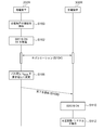
- FIG. 2 is an operation sequence diagram of the power supply system 100 of FIG.
- the power feeding side controller 204 detects the connection based on the state of the CC port (S100). Specifically, the power receiving side controller 310 of the power receiving device 300R stands by in a state where the CC port is pulled down by a pull-down resistor (terminating resistor) Rd having a predetermined resistance value.
- a pull-down resistor Rd on the power receiving device 300R side and a voltage corresponding to its own state are generated in the CC port of the power receiving device 200R.
- the power feeding side controller 204 of the power feeding device 200R can detect the connection of the power receiving device 300R (electronic device 400).
- the bus switch SW1 is turned on (S102) to supply the default bus voltage V BUS of 5 V.
- the power receiving side controller 310 can operate.
- the power supply side controller 204 and the power reception side controller 310 negotiate to determine the bus voltage V BUS based on the required voltage (S104).
- the power supply side controller 204 changes the bus voltage V BUS from the initial voltage of 5 V to the required voltage (S106).
- the power feeding side controller 204 notifies the power receiving side controller 310 (S108). In response to this notification, the power receiving side controller 310 turns on the bus switch SW2 (S110). As a result, the bus voltage V BUS is supplied to the charging circuit 302 and the load circuit 406 (S112).
- FIG. 3 is a circuit diagram of the PD controller 500.
- the PD controller 500 includes a logic circuit 510, pull-down resistors Rd 1 and Rd 2 , and transistors Md 1 and Md 2 .
- the logic circuit 510 controls the on / off of the transistors Md 1 and Md 2 .
- the transistors Md 1 and Md 2 are turned on, the CC1 port and the CC2 port are pulled down by the resistors Rd 1 and Rd 2 .
- the PD controller 500 is mounted on the electronic device 400 of FIG. 1 and used as the power receiving side controller 310.
- the logic circuit 510 operates using the voltage supplied to the power supply terminal VCS of the PD controller 500 as a power source.
- the logic circuit 510 becomes inoperable, so that the transistors Md 1 and Md 2 cannot be turned on. Therefore, the PD controller 500 is provided with voltage clamp circuits 520_1 and 520_2.
- the voltage clamp circuits 520_1 and 520_2 are activated in the dead battery state, and the CC1 port and CC2 port are pulled down by the pull-down resistors R2 1 and R2 2 .
- the voltage clamp circuits 520_1 and 520_2 are similarly configured.
- the transistor M2 # is turned on, the transistor M1 # is turned off, and the voltage clamp circuit 520_ # is inactive.
- the transistor M2 # cannot be kept on.
- the voltage clamp circuit 520_ # is active.
- the power supply side controller 204 of the power feeding device 200R is connected, the gate of the transistor M1 # is pulled up via the resistor R3 #, the transistor M1 # is turned on.
- the resistor R2 # is connected to the CC # port as a terminating resistor.
- the PD controller 500 is configured to be operable as both the power feeding side controller 204 and the power receiving side controller 310 in FIG. If the PD controller 500 is used as the power supply side controller 204, it is desirable to stop (disable) the functions of the voltage clamp circuits 520_1 and 520_2 because there is no dead battery state. Therefore, the gate of the transistor M1 # is connected to the enable pin EN #. By connecting the enable pin EN # to an external ground, the transistor M1 # can be fixedly turned off and the voltage clamp circuit 520_ # can be disabled. When the PD controller 500 is used as the power receiving side controller 310, the enable pin EN # may be opened.
- the setting of the state (enable / disable) of the voltage clamp circuits 520_1 and 520_2 is common, it can be originally set by one enable pin EN. However, the gate of transistor M1 1 and M1 2, can not be connected to a common one of the enable pin EN. This is because it causes mutual interference between the voltage clamp circuits 520_1 and 520_2.
- the present invention has been made in view of the above problems, and one of the exemplary purposes of the present invention is to provide a terminal circuit capable of setting an enable state and a disable state with a single enable pin.
- the semiconductor integrated circuit includes a plurality of target pins to be terminated, an enable pin, and a plurality of termination circuits corresponding to the plurality of target pins.
- the plurality of termination circuits consist of a first resistor and a first transistor provided in series between the corresponding target pin and the ground, and a second resistor provided between the corresponding target pin and the control electrode of the first transistor, respectively.
- the semiconductor integrated circuit includes a plurality of target pins to be terminated, an enable pin, and a plurality of termination circuits corresponding to the plurality of target pins.
- the plurality of termination circuits consist of a first resistor and a first transistor provided in series between the corresponding target pin and the ground, and a second resistor provided between the corresponding target pin and the control electrode of the first transistor, respectively.
- the output node is connected to the control electrode of the first transistor, (i) has an output impedance greater than the second resistor when the enable pin is in the first state, and (ii) the enable pin is in the second state.
- the semiconductor integrated circuit includes a plurality of target pins to be terminated, an enable pin, and a plurality of termination circuits corresponding to the plurality of target pins.
- the plurality of termination circuits consist of a first resistor and a first transistor provided in series between the corresponding target pin and the ground, and a second resistor provided between the corresponding target pin and the control electrode of the first transistor, respectively.
- the enable pin When the enable pin is set to the first state, the current synced by the enable circuit causes a voltage drop in the second resistor, and a voltage slightly lower than the voltage of the target pin is generated in the control electrode of the first transistor.
- the transistor can be turned on. That is, the terminal circuit is in the enabled state.
- the enable pin When the enable pin is set to the second state, the output node, that is, the control electrode of the first transistor is fixed to low, and the first transistor can be fixed to off. That is, the terminal circuit is disabled.
- mutual interference between a plurality of terminal circuits can be suppressed by interposing an enable circuit, and an enable state and a disable state of a plurality of terminal circuits can be set with a single enable pin.
- the enable circuit has (i) an output impedance greater than the second resistor when the enable pin is in the first state, and (ii) a second when the enable pin is in the second state. It can be said that it has an output impedance smaller than that of a resistor.
- the enable circuit may include a second transistor provided between the output node and the ground, and a bias circuit that changes the state of the second transistor according to the state of the enable pin.
- the bias circuit applies a relatively low voltage to the control electrode of the second transistor when the enable pin is in the first state, and relatively to the control electrode of the second transistor when the enable pin is in the second state. It may be configured to apply a high voltage. This makes it possible to change the output impedance of the enable circuit.
- the bias circuit includes a third resistor whose one end is connected to the target pin and a third transistor whose high potential side electrode and control electrode are connected to the other end of the third resistor and whose low potential side electrode is connected to the enable pin. , May be included.
- the back gate of the third transistor may be grounded.
- the isolation between the plurality of target pins can be enhanced by the body diode between the back gate and the source of the third transistor.
- the enable circuit may include a current mirror circuit that folds back the current flowing from the target pin to the enable pin and sinks it from the output node.
- a current flows to the input side of the current mirror circuit, which can be folded back to sink the current from the output node.
- the enable pin is open, no current flows to the input side of the current mirror circuit and the output node is fixed low.
- the enable pin may be low or high impedance.
- Each of the plurality of termination circuits may further include a Zener diode provided between the control electrode of the first transistor and the ground. This can protect the circuit element.
- the "state in which the member A is connected to the member B" means that the member A and the member B are physically directly connected, or the member A and the member B are electrically connected to each other. It also includes the case of being indirectly connected via other members, which does not substantially affect the connection state or does not impair the functions and effects performed by the combination thereof.
- a state in which the member C is provided between the member A and the member B means that the member A and the member C, or the member B and the member C are directly connected, and their electricity. It also includes the case of being indirectly connected via other members, which does not substantially affect the connection state, or does not impair the functions and effects performed by the combination thereof.
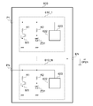
- FIG. 4 is a circuit diagram of the semiconductor integrated circuit 600 according to the embodiment.
- the semiconductor integrated circuit 600 includes a plurality of N target pins P1 to PN (N ⁇ 2) to be terminated, an enable pin EN, and a plurality of termination circuits 610_1 to 610_N corresponding to the plurality of target pins P1 to PN. Be prepared.
- the plurality of terminal circuits 610_1 to 610_N are similarly configured.
- the first resistor R1 and the first transistor M1 are provided in series between the corresponding target pin P # and ground.
- the second resistor R2 is provided between the corresponding target pin P # and the control electrode (gate) of the first transistor M1.
- the output node 622 of the enable circuit 620 is connected to the gate of the first transistor M1.
- the enable circuit 620 (i) sinks the current Is from the output node 622 when the enable pin EN is in the first state (for example, ground), and (ii) when the enable pin EN is in the second state (for example, open).
- the output node 622 is configured to be fixed low.
- the Zener diode ZD1 is provided between the gate of the first transistor M1 and the ground.
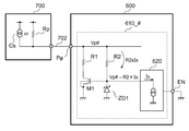
- FIG. 5 is an equivalent circuit diagram of the semiconductor integrated circuit 600 when the enable pin EN is in the first state. Only pin P # and related parts are shown here.
- the target pin P # of the semiconductor integrated circuit 600 is connected to the pin 704 of the external circuit 700 via the wiring 702. Inside the external circuit 700, the pin 704 is pulled up by a pull-up resistor Rp or connected to the source current source CS. The voltage generated at the target pin P # at this time is defined as Vp #.
- the gate voltage Vg1 of the first transistor M1 is Vp # ⁇ R2 ⁇ Is.
- Vgs (th) is the threshold voltage between the gate and source of the N-channel MOSFET (Metal Oxide Semiconductor Field Effect Transistor).
- MOSFET Metal Oxide Semiconductor Field Effect Transistor
- FIG. 6 is an equivalent circuit diagram of the semiconductor integrated circuit 600 when the enable pin EN is in the second state.
- the output impedance of the enable circuit 620 is sufficiently smaller than the resistance value of the second resistor R2.
- the output node 622 of the enable circuit 620 is fixed to low (near the ground voltage 0V).
- the first transistor M1 can be turned off.
- the target pin P # is not terminated (pulled down) by the resistor R1, and therefore the termination circuit 610_ # is disabled.
- the enable state and the disable state of the plurality of terminal circuits 610_1 to 610_N can be set by one enable pin EN. Further, by interposing the enable circuit 620 between the gate of the first transistor M1 and the enable pin EN, mutual interference of a plurality of terminal circuits 610_1 to 610_N can be suppressed.
- the Zener diode ZD1 when a high voltage is generated at the target pin P #, the voltage of the gate of the first transistor M1 and the output node of the enable circuit 620 can be clamped, and the voltage of the first transistor M1 and the enable The internal element of the circuit 620 can be protected.
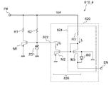
- FIG. 7 is a circuit diagram showing a specific configuration example of the enable circuit 620.
- the enable circuit 620 includes a second transistor M2 provided between the output node 622 and the ground, and a bias circuit 624 that changes the state of the second transistor M2 according to the state of the enable pin EN.
- the enable circuit 620 applies a relatively low voltage VL to the gate of the second transistor M2 when the enable pin EN is in the first state (short), and when the enable pin EN is in the second state (open). , A relatively high voltage VH is applied to the gate of the second transistor M2.
- the bias circuit 624 includes a third resistor R3 and a third transistor M3. One end of the third resistor R3 is connected to the target pin P #. In the third transistor M3, the electrode (drain) on the high potential side and the control electrode (gate) are connected to the other end of the third resistor R3, and the electrode (source) on the low potential side is connected to the enable pin EN.
- the back gate of the third transistor M3 is grounded.
- Transistors M2 and M3 form a current mirror circuit 626.
- the size ratio of the transistors M2 and M3 is 1: N.
- FIG. 8 is a circuit diagram showing another configuration example of the terminal circuit 610_ #.
- the third transistor M3 of FIG. 7 is replaced by the rectifier circuit D1.
- the rectifier circuit D1 includes one or a plurality of diodes connected in series.
- Vf When the enable pin EN is grounded, the forward voltage Vf of the rectifier circuit D1 is applied to the gate of the second transistor M2.
- Vf may be designed so that an appropriate sink current Is flows through the second transistor M2.
- the enable pin EN When the enable pin EN is open, the high voltage Vp # of the target pin P # is applied to the gate of the second transistor M2 via the third resistor R3. As a result, the second transistor M2 is fully turned on.
- the rectifier circuit D1 may be replaced with a resistor (the resistance value is R4).
- FIG. 9 is a circuit diagram showing another configuration example of the terminal circuit 610_ #.
- the enable circuit 620 has (i) an output impedance Ro1 larger than the second resistor R2 when the enable pin EN is in the first state, and (ii) from the second resistor R2 when the enable pin is in the second state. It has a small output impedance Ro2.
- Ro1 R2
- the gate voltage Vg1 becomes high and the first transistor M1 can be turned on.
- Ro2 R2
- the gate voltage Vg1 becomes low and the first transistor M1 can be turned off.
- the enable circuit 620 includes a variable impedance element 628 provided between the output node 622 and the ground, and an impedance control unit 630 that controls the impedance of the variable impedance element 628 (that is, the output impedance Ro of the enable circuit 620).
- the impedance control unit 630 changes the impedance Ro of the variable impedance element 628 according to the state of the enable pin EN.
- FIG. 10 is a circuit diagram of a USB (Universal Serial Bus) PD (Power Delivery) controller 800.
- the PD controller 800 is used as the power receiving side controller 310 or the power feeding side controller 204 in FIG.
- the PD controller 800 has two CC (Configuration Channel) pins CC1 and CC2.
- the PD controller 800 includes a logic circuit 810, pull-down circuits 820_1 and 820_2, and a voltage clamp circuit 830_1 and 830_2.
- the battery voltage or the power supply voltage generated based on the battery voltage is supplied to the power supply terminal VCS of the logic circuit 810.
- the logic circuit 810 controls the state of the pull-down circuits 820_1 and 820_2 when the power supply voltage is higher than the UVLO (low voltage lockout) threshold value. Further, the fourth transistor M4 of the voltage clamp circuits 830_1 and 830_2 is fixed on, and the voltage clamp circuits 830_1 and 830_2 are invalidated.
- the voltage clamp circuits 830_1 and 830_2 correspond to the terminal circuit 610 described above.
- the voltage clamp circuits 830_1 and 830_2 are connected to a common enable pin EN to control enable / disable.
- the enable pin EN is set to the first state.
- the CC1 pin and the CC2 pin can be pulled down when the logic circuit 810 is inoperable in the dead battery state.
- the enable pin EN is in the second state.
- the voltage clamp circuits 830_1 and 830_2 are disabled.
- FIG. 11 is a diagram showing an electronic device 900 including a power receiving device 300.
- the electronic device 900 illustrated here is a smartphone or a tablet terminal.
- the electronic device 900 includes a receptacle 902, a housing 904, a display panel 906, a CPU 910, and a baseband IC 912, in addition to the battery 402 and the power receiving device 300 described above.
- the power receiving device 300 receives the bus voltage supplied to the receptacle 902, charges the battery 402, and supplies the power supply voltage to the load such as the CPU 910 and the baseband IC 912.
- the electronic device 900 may be a notebook PC, a digital camera, a digital video camera, an audio player, or the like.
- the present invention relates to an electronic circuit.
- Power supply system 102 Adapter 106 USB cable 108 Receptor 200 Power supply device 202 Power supply circuit 204 Power supply side controller SW1 Bus switch 206 5V power supply 400 Electronic equipment 402 Battery 404 Transistor 406 Load 300 Power receiving device 302 Charging circuit 310 Power receiving side controller SW2 Bus switch 900 Electronic Equipment 500 PD controller 520 Voltage clamp circuit 600 Semiconductor integrated circuit P1, P2 Target pin EN Enable pin 610 Termination circuit M1 1st transistor M2 2nd transistor M3 3rd transistor M4 4th transistor R1 1st resistance R2 2nd resistance R3 3rd Resistance 620 Enable circuit 622 Output node 624 Bias circuit 630 Impedance control unit 800 PD controller 810 Logic circuit 820 Pull-down circuit 830 Voltage clamp circuit
Landscapes
- Engineering & Computer Science (AREA)
- Theoretical Computer Science (AREA)
- General Engineering & Computer Science (AREA)
- Physics & Mathematics (AREA)
- General Physics & Mathematics (AREA)
- Power Engineering (AREA)
- Computer Hardware Design (AREA)
- Semiconductor Integrated Circuits (AREA)
- Power Sources (AREA)
- Metal-Oxide And Bipolar Metal-Oxide Semiconductor Integrated Circuits (AREA)
Abstract
半導体集積回路600は、複数の対象ピンP1~P#に対応する複数の終端回路610_1~610_Nを備える。複数の終端回路610_1~610_Nはそれぞれ、対応する対象ピンP#と接地の間に直列に設けられた第1抵抗R1および第1トランジスタM1を備える。対応する対象ピンP#と第1トランジスタM1の制御電極の間には、第2抵抗R2が設けられる。イネーブル回路620は、その出力ノード622が第1トランジスタM1の制御電極と接続されており、(i)イネーブルピンENが第1状態であるとき、出力ノード622から電流Isをシンクし、(ii)イネーブルピンが第2状態であるとき、出力ノード622をローに固定する。
Description
本発明は、終端回路に関する。
携帯電話端末、スマートホン、タブレット端末、ノート型コンピュータ、ポータブルオーディオプレイヤをはじめとする電池駆動デバイスは、再充電可能な二次電池とともに、それを充電するための充電回路を内蔵する。充電回路には、外部からUSBケーブルを介して供給されたDC電圧(バス電圧VBUS)や、外部のACアダプタからのDC電圧にもとづいて二次電池を充電するものが存在する。
現在、モバイル機器に搭載される充電回路は、USB Battery Charging Specificationと呼ばれる規格(以下、BC規格という)に準拠したものが主流である。USBホストあるいはチャージャ(以下、USB給電装置と総称する)には、いくつかの種類が存在する。BC revision 1.2規格においては、USB給電装置の種類として、SDP(Standard Downstream Port)、DCP(Dedicated Charging Port)、CDP(Charging Downstream Port)が定義されている。そしてUSB給電装置が供給できる電流(電流容量)は、その種類に応じて規定されている。具体的には、DCP、CDPでは1500mA、SDPでは、USBのバージョンに応じて100mA、500mA、900mAのように規定されている。
USBを利用した二次電池充電の方式、システムとして、USB Power Deliveryと呼ばれる規格(以下、USB-PD規格という)が策定されている。USB-PD規格では、供給可能な電力がBC規格の7.5Wから、最大100Wまで大幅に増大する。具体的にはUSB-PD規格では、USBバス電圧として、5Vより高い電圧(具体的には、9V,12V,15V,20V等)の供給が許容されており、充電電流も、BC規格よりも大きな量(具体的には、2A,3A、5A等)の供給が許容される。USB-PD規格は、USB type-C規格にも採用されている。
図1は、給電システム100Rのブロック図である。この給電システム100Rは、USB Type-C規格に準拠しており、USBケーブル106を介して接続される給電装置200Rと受電装置300Rを備える。たとえば給電装置200RはACアダプタ102に搭載され、あるいは電子機器に搭載される。受電装置300Rは、スマートホン、タブレット端末、デジタルカメラ、デジタルビデオカメラ、ポータブルオーディオプレイヤなど、電池駆動型の電子機器400に搭載される。
給電装置200Rは、電源回路202、給電側のPDコントローラ(以下、給電側コントローラという)204およびバススイッチSW1を含む。電子機器400のレセプタクル108にはUSBケーブル106が着脱可能に接続される。なおレセプタクル108が省略され、USBケーブル106がACアダプタ102と一体となっている充電アダプタも存在する。
レセプタクル108は、バス電圧VBUSを供給するためのVBUS端子、接地電圧VGNDを供給するためのGND端子ならびにCC(Configuration Channel)ポートを含む。実際には、CCポートは2個設けられるが、図1では1個に簡略化して示す。電源回路202は、バス電圧VBUSを発生する。電源回路202は、図示しない外部電源(たとえば商用交流電源)からのAC100Vを受け、それを直流のバス電圧VBUSに変換するAC/DCコンバータを含んでもよい。電源回路202が発生したバス電圧VBUSは、USBケーブル106のバスラインおよびバススイッチSW1を介して受電装置300Rに供給される。
給電側コントローラ204および受電側コントローラ310はそれぞれ、USB Type-Cに関するポートコントローラであり、CCラインを介して互いに接続され、通信機能を提供する。給電側コントローラ204と受電側コントローラ310は、給電装置200Rが供給すべきバス電圧VBUSの電圧レベルをネゴシエートする。給電側コントローラ204は、決定した電圧レベルが得られるように電源回路202を制御し、またバススイッチSW1のオン、オフを制御する。
電子機器400は、バッテリ402、レセプタクル404、負荷(システム)406および受電装置300Rを備える。バッテリ402は再充電可能な2次電池である。負荷回路406は、CPUやメモリ、液晶ディスプレイ、オーディオ回路などを含む。レセプタクル404にはUSBケーブル106を介してACアダプタ102が着脱可能に接続される。
受電装置300Rは、アダプタ102からの電力を受け、充電回路302を充電する。受電装置300Rは、充電回路302、受電側コントローラ310、バススイッチSW2を備える。
充電回路302は、USBケーブル106およびバススイッチSW2を介して給電装置200Rからのバス電圧VBUS(受電装置300R側において、アダプタ電圧VADPとも表記する)を受け、バッテリ402を充電する。充電回路302は、降圧DC/DCコンバータ、リニアレギュレータあるいはそれらの組み合わせで構成される。
充電回路302から負荷回路406へは、アダプタ電圧VADPおよびバッテリ402の電圧VBATの少なくとも一方に応じたシステム電圧VSYSが供給される。負荷回路406は、パワーマネージメントIC(Integrated Circuit)、DC/DCコンバータやリニアレギュレータなどを含むマルチチャンネル電源や、マイコン、液晶ディスプレイ、ディスプレイドライバなどを含む。
受電側コントローラ310には、受電装置300Rが要求するバス電圧VBUSおよび最大電流を規定するデータ(要求PDO:Power Data Object)が規定されている。ACアダプタ102と電子機器400が接続されると、給電側コントローラ204と受電側コントローラ310とがネゴシエーションを行い、要求PDOにもとづいてバス電圧VBUSの電圧レベルが決定される。また受電側コントローラ310は、バススイッチSW2のオン、オフを制御する。
図2は、図1の給電システム100の動作シーケンス図である。給電装置200Rと受電装置300RがUSBケーブル106を介して接続されると、給電側コントローラ204は、CCポートの状態にもとづいてその接続を検出する(S100)。具体的には、受電装置300Rの受電側コントローラ310は、CCポートを、所定の抵抗値を有するプルダウン抵抗(終端抵抗)Rdによってプルダウンした状態で待機する。給電装置200Rと受電装置300Rが接続されると、給電装置200RのCCポートには、受電装置300R側のプルダウン抵抗Rdと、自分自身の状態に応じた電圧が発生する。これをもって給電装置200Rの給電側コントローラ204は、受電装置300R(電子機器400)の接続を検出できる。
そしてバススイッチSW1をオンし(S102)、デフォルトの5Vのバス電圧VBUSを供給する。バススイッチSW1がオンすると、受電側コントローラ310が動作可能となる。
続いて、給電側コントローラ204と受電側コントローラ310がネゴシエーションを行い、要求電圧にもとづいてバス電圧VBUSを決定する(S104)。給電側コントローラ204は、バス電圧VBUSを、5Vの初期電圧から要求電圧に変更する(S106)。
バス電圧VBUSの要求電圧への変更が完了すると、そのことが給電側コントローラ204から受電側コントローラ310に通知される(S108)。受電側コントローラ310は、この通知に応答して、バススイッチSW2をオンする(S110)。これにより充電回路302および負荷回路406にバス電圧VBUSが供給される(S112)。
図3は、PDコントローラ500の回路図である。PDコントローラ500は、ロジック回路510、プルダウン抵抗Rd1,Rd2、トランジスタMd1,Md2を備える。
ロジック回路510は、トランジスタMd1,Md2のオン、オフを制御する。トランジスタMd1,Md2がオンとなると、CC1ポートとCC2ポートは、抵抗Rd1,Rd2によってプルダウンされる。
PDコントローラ500が、図1の電子機器400に搭載され、受電側コントローラ310として使用される場合を考える。ロジック回路510は、PDコントローラ500の電源端子VCCに供給される電圧を電源として動作する。バッテリ402の残量がゼロのデッドバッテリー状態では、ロジック回路510が動作不能となるため、トランジスタMd1,Md2をオンできなくなる。そこで、PDコントローラ500には、電圧クランプ回路520_1,520_2が設けられる。
電圧クランプ回路520_1,520_2は、デッドバッテリー状態においてアクティブとなり、CC1ポート、CC2ポートを、プルダウン抵抗R21,R22によってプルダウンする。電圧クランプ回路520_1,520_2は同様に構成される。
電圧クランプ回路520_#(#=1,2)は、抵抗R2#,R3#,トランジスタM1#,M2#を含む。バッテリ残量が残っており、ロジック回路510が動作可能であるとき、トランジスタM2#はオンされ、トランジスタM1#がオフとなり、電圧クランプ回路520_#は非アクティブとなる。
デッドバッテリー状態においてロジック回路510が動作不能となると、トランジスタM2#のオンが維持できなくなる。トランジスタM2#がオフの状態は、電圧クランプ回路520_#がアクティブの状態である。対応するCC#ポートに、給電装置200Rの給電側コントローラ204が接続されると、トランジスタM1#のゲートが、抵抗R3#を介してプルアップされ、トランジスタM1#がオンとなる。これにより抵抗R2#が終端抵抗としてCC#ポートに接続される。
PDコントローラ500は、図1の給電側コントローラ204としても、受電側コントローラ310としても動作可能に構成される。もしPDコントローラ500を給電側コントローラ204として用いる場合、デッドバッテリー状態は存在しないから、電圧クランプ回路520_1,520_2の機能を停止(ディセーブル)することが望まれる。そのために、トランジスタM1#のゲートは、イネーブルピンEN#と接続される。イネーブルピンEN#を外部の接地と接続することにより、トランジスタM1#が固定的にオフとなり、電圧クランプ回路520_#をディセーブルとすることができる。PDコントローラ500を受電側コントローラ310として使用する場合、イネーブルピンEN#をオープンとすればよい。
ここで、電圧クランプ回路520_1,520_2の状態(イネーブル/ディセーブル)の設定は共通であるため、本来的には、1個のイネーブルピンENで設定することができる。しかしながら、トランジスタM11とM12のゲートを、共通の1個のイネーブルピンENに接続することはできない。なぜなら電圧クランプ回路520_1,520_2の相互干渉を引き起こすからである。
本発明はかかる課題に鑑みてなされたものであり、そのある態様の例示的な目的のひとつは、単一のイネーブルピンで、イネーブル状態、ディセーブル状態を設定可能な終端回路の提供にある。
本発明のある態様は、半導体集積回路に関する。半導体集積回路は、終端すべき複数の対象ピンと、イネーブルピンと、複数の対象ピンに対応する複数の終端回路と、を備える。複数の終端回路はそれぞれ、対応する対象ピンと接地の間に直列に設けられた第1抵抗および第1トランジスタと、対応する対象ピンと第1トランジスタの制御電極の間に設けられた第2抵抗と、出力ノードが第1トランジスタの制御電極と接続され、(i)イネーブルピンが第1状態であるとき、出力ノードから電流をシンクし、(ii)イネーブルピンが第2状態であるとき、出力ノードをローに固定するイネーブル回路と、を備える。
本発明のある態様は、半導体集積回路に関する。半導体集積回路は、終端すべき複数の対象ピンと、イネーブルピンと、複数の対象ピンに対応する複数の終端回路と、を備える。複数の終端回路はそれぞれ、対応する対象ピンと接地の間に直列に設けられた第1抵抗および第1トランジスタと、対応する対象ピンと第1トランジスタの制御電極の間に設けられた第2抵抗と、出力ノードが第1トランジスタの制御電極と接続されており、(i)イネーブルピンが第1状態であるとき、第2抵抗より大きい出力インピーダンスを有し、(ii)イネーブルピンが第2状態であるとき、出力ノードをローに固定するイネーブル回路と、を備える。
本発明のある態様によれば、単一のイネーブルピンで、複数の終端回路のイネーブル状態、ディセーブル状態を設定できる。
(実施の形態の概要)
本明細書に開示される一実施の形態は、半導体集積回路に関する。半導体集積回路は、終端すべき複数の対象ピンと、イネーブルピンと、複数の対象ピンに対応する複数の終端回路と、を備える。複数の終端回路はそれぞれ、対応する対象ピンと接地の間に直列に設けられた第1抵抗および第1トランジスタと、対応する対象ピンと第1トランジスタの制御電極の間に設けられた第2抵抗と、出力ノードが第1トランジスタの制御電極と接続され、(i)イネーブルピンが第1状態であるとき、出力ノードから電流をシンクし、(ii)イネーブルピンが第2状態であるとき、出力ノードをローに固定するイネーブル回路と、を備える。
本明細書に開示される一実施の形態は、半導体集積回路に関する。半導体集積回路は、終端すべき複数の対象ピンと、イネーブルピンと、複数の対象ピンに対応する複数の終端回路と、を備える。複数の終端回路はそれぞれ、対応する対象ピンと接地の間に直列に設けられた第1抵抗および第1トランジスタと、対応する対象ピンと第1トランジスタの制御電極の間に設けられた第2抵抗と、出力ノードが第1トランジスタの制御電極と接続され、(i)イネーブルピンが第1状態であるとき、出力ノードから電流をシンクし、(ii)イネーブルピンが第2状態であるとき、出力ノードをローに固定するイネーブル回路と、を備える。
イネーブルピンを第1状態に設定すると、イネーブル回路がシンクする電流によって、第2抵抗に電圧降下が発生し、第1トランジスタの制御電極に対象ピンの電圧よりわずかに低い電圧を発生し、第1トランジスタをオンさせることができる。つまり終端回路はイネーブル状態となる。イネーブルピンを第2状態に設定すると、出力ノード、すなわち第1トランジスタの制御電極がローに固定され、第1トランジスタをオフに固定することができる。つまり終端回路はディセーブル状態となる。この実施の形態によれば、イネーブル回路を介在させることにより、複数の終端回路間の相互干渉を抑制でき、単一のイネーブルピンで、複数の終端回路のイネーブル状態、ディセーブル状態を設定できる。
別の観点から見ると、イネーブル回路は、(i)イネーブルピンが第1状態であるとき、第2抵抗より大きい出力インピーダンスを有し、(ii)イネーブルピンが第2状態であるとき、第2抵抗より小さい出力インピーダンスを有すると言える。
イネーブル回路は、出力ノードと接地の間に設けられた第2トランジスタと、イネーブルピンの状態に応じて、第2トランジスタの状態を変化させるバイアス回路と、を含んでもよい。
バイアス回路は、イネーブルピンが第1状態であるとき、第2トランジスタの制御電極に相対的に低い電圧を印加し、イネーブルピンが第2状態であるとき、第2トランジスタの制御電極に相対的に高い電圧を印加するように構成されてもよい。これによりイネーブル回路の出力インピーダンスを変化させることができる。
バイアス回路は、一端が対象ピンと接続される第3抵抗と、高電位側の電極および制御電極が第3抵抗の他端と接続され、低電位側の電極がイネーブルピンと接続される第3トランジスタと、を含んでもよい。
第3トランジスタのバックゲートは接地されてもよい。これにより、第3トランジスタのバックゲートとソース間のボディダイオードによって、複数の対象ピン間のアイソレーションを高めることができる。
イネーブル回路は、前記対象ピンから前記イネーブルピンに流れる電流を折り返し、出力ノードからシンクするカレントミラー回路を含んでもよい。イネーブルピンが接地されるとき、カレントミラー回路の入力側に電流が流れ、それが折り返されて、出力ノードから電流をシンクできる。イネーブルピンがオープンであるとき、カレントミラー回路の入力側には電流が流れず、出力ノードはローに固定される。
イネーブルピンは、ローまたはハイインピーダンスとされてもよい。
複数の終端回路はそれぞれ、第1トランジスタの制御電極と接地の間に設けられたツェナーダイオードをさらに備えてもよい。これにより回路素子を保護できる。
以下、本発明を好適な実施の形態をもとに図面を参照しながら説明する。各図面に示される同一または同等の構成要素、部材、処理には、同一の符号を付するものとし、適宜重複した説明は省略する。また、実施の形態は、発明を限定するものではなく例示であって、実施の形態に記述されるすべての特徴やその組み合わせは、必ずしも発明の本質的なものであるとは限らない。
本明細書において、「部材Aが、部材Bと接続された状態」とは、部材Aと部材Bが物理的に直接的に接続される場合や、部材Aと部材Bが、それらの電気的な接続状態に実質的な影響を及ぼさない、あるいはそれらの結合により奏される機能や効果を損なわせない、その他の部材を介して間接的に接続される場合も含む。
同様に、「部材Cが、部材Aと部材Bの間に設けられた状態」とは、部材Aと部材C、あるいは部材Bと部材Cが直接的に接続される場合のほか、それらの電気的な接続状態に実質的な影響を及ぼさない、あるいはそれらの結合により奏される機能や効果を損なわせない、その他の部材を介して間接的に接続される場合も含む。
図4は、実施の形態に係る半導体集積回路600の回路図である。半導体集積回路600は、終端すべき複数N個(N≧2)の対象ピンP1~PNと、イネーブルピンENと、複数の対象ピンP1~PNに対応する複数の終端回路610_1~610_Nと、を備える。複数の終端回路610_1~610_Nは同様に構成される。
複数の終端回路610_#(#=1,…N)はそれぞれ、第1抵抗R1、第1トランジスタM1、第2抵抗R2、ツェナーダイオードZD1、イネーブル回路620を備える。第1抵抗R1および第1トランジスタM1は、対応する対象ピンP#と接地の間に直列に設けられる。第2抵抗R2は、対応する対象ピンP#と第1トランジスタM1の制御電極(ゲート)の間に設けられる。
イネーブル回路620はその出力ノード622が第1トランジスタM1のゲートと接続される。イネーブル回路620は、(i)イネーブルピンENが第1状態(たとえば接地)であるとき、出力ノード622から電流Isをシンクし、(ii)イネーブルピンENが第2状態(たとえばオープン)であるとき、出力ノード622をローに固定するように構成される。
ツェナーダイオードZD1は、第1トランジスタM1のゲートと接地の間に設けられる。
以上が半導体集積回路600の構成である。続いてその動作を説明する。図5は、イネーブルピンENが第1状態であるときの半導体集積回路600の等価回路図である。ここではピンP#とそれに関する部分のみを示す。使用において半導体集積回路600の対象ピンP#は、配線702を介して、外部回路700のピン704と接続される。外部回路700の内部において、ピン704は、プルアップ抵抗Rpによってプルアップされ、あるいはソース電流源CSと接続される。このときに対象ピンP#に発生する電圧をVp#とする。
イネーブル回路620が電流Isをシンクすることにより、第2抵抗R2には、電圧降下R2×Isが発生する。したがって、第1トランジスタM1のゲート電圧Vg1は、Vp#-R2×Isとなる。
Vg1>Vgs(th)となるように、言い換えれば、Vp#-R2×Is>Vgs(th)が成り立つように、抵抗値R2,電流量Isが定められる。Vgs(th)はNチャンネルMOSFET(Metal Oxide Semiconductor Field Effect Transistor)のゲートソース間しきい値電圧である。これにより第1トランジスタM1をオンすることができる。つまり対象ピンP#は抵抗R1によって終端(プルダウン)され、終端回路610_#はイネーブル状態となる。
図6は、イネーブルピンENが第2状態であるときの半導体集積回路600の等価回路図である。
第2状態において、イネーブル回路620の出力インピーダンスは、第2抵抗R2の抵抗値より十分に小さくなる。これによりイネーブル回路620の出力ノード622はロー(接地電圧0V付近)に固定される。これにより、第1トランジスタM1をオフすることができる。このとき、対象ピンP#は抵抗R1によって終端(プルダウン)されず、したがって終端回路610_#はディセーブル状態となる。
以上が半導体集積回路600の動作である。この半導体集積回路600によれば、複数の終端回路610_1~610_Nのイネーブル状態、ディセーブル状態を、ひとつのイネーブルピンENによって設定できる。また、第1トランジスタM1のゲートとイネーブルピンENの間にイネーブル回路620を介在させることにより、複数の終端回路610_1~610_Nの相互干渉を抑制できる。
またツェナーダイオードZD1を設けることにより、対象ピンP#に高電圧が発生したときに、第1トランジスタM1のゲートおよびイネーブル回路620の出力ノードの電圧をクランプすることができ、第1トランジスタM1およびイネーブル回路620の内部素子を保護することができる。
図7は、イネーブル回路620の具体的な構成例を示す回路図である。イネーブル回路620は、出力ノード622と接地の間に設けられた第2トランジスタM2と、イネーブルピンENの状態に応じて、第2トランジスタM2の状態を変化させるバイアス回路624と、を含む。
イネーブル回路620は、イネーブルピンENが第1状態(ショート)であるとき、第2トランジスタM2のゲートに相対的に低い電圧VLを印加し、イネーブルピンENが第2状態(オープン)であるとき、第2トランジスタM2のゲートに相対的に高い電圧VHを印加するように構成される。
バイアス回路624は、第3抵抗R3と第3トランジスタM3を含む。第3抵抗R3の一端は、対象ピンP#と接続される。第3トランジスタM3は、高電位側の電極(ドレイン)および制御電極(ゲート)が第3抵抗R3の他端と接続され、低電位側の電極(ソース)がイネーブルピンENと接続される。
好ましくは第3トランジスタM3のバックゲートは接地される。これにより、第3トランジスタM3のバックゲートとソース間のボディダイオードBDによって、複数の対象ピンP#(#=1~N)間のアイソレーションを高めることができる。
以上が終端回路610の構成例である。続いてその動作を説明する。トランジスタM2とM3は、カレントミラー回路626を構成する。トランジスタM2とM3のサイズ比を1:Nとする。このカレントミラー回路626は、対象ピンP#からイネーブルピンENに流れる電流I1を折り返し、1/N倍の電流Is(=I1/N)を出力ノード622からシンクする。
イネーブルピンENが接地される第1状態では、対象ピンP#から接地に対して電流経路(第3抵抗R3および第3トランジスタM3)が有効になるから、電流I1が流れ、それに比例する電流Isが出力ノード622からシンクされ、第1トランジスタM1のゲートに高い電圧を発生し、第1トランジスタM1をオンすることができる。
イネーブルピンENがオープン(あるいは高電位が印加される)となる第2状態では、対象ピンP#から接地に対して電流経路が存在しない。したがって電流I1が流れず、第2トランジスタM2のゲートは第3抵抗R3によって高電圧Vp#にプルアップされる。これにより、第2トランジスタM2がフルオンし、第1トランジスタM1のゲートがローに固定される。
図8は、終端回路610_#の別の構成例を示す回路図である。図8において図7の第3トランジスタM3は、整流回路D1に置換されている。整流回路D1は、ひとつあるいは直列に接続される複数のダイオードを含む。整流回路D1は、イネーブルピンENが接地されるときに、電位差ΔV(=Vf)を発生する定電圧源と把握することもできる。
イネーブルピンENが接地されるとき、第2トランジスタM2のゲートには、整流回路D1の順方向電圧Vfが印加される。Vfは、第2トランジスタM2に適切なシンク電流Isが流れるように設計すればよい。
イネーブルピンENがオープンのとき、第2トランジスタM2のゲートには、第3抵抗R3を介して、対象ピンP#の高電圧Vp#が印加される。これにより第2トランジスタM2はフルオンする。
なお対象ピンP#の高電圧Vp#が予め規定されているアプリケーションでは、整流回路D1を抵抗(抵抗値をR4とする)で置換してもよい。イネーブルピンENが接地されるとき、抵抗R3とR4が形成する分圧回路によって電圧Vp#が分圧され、分圧後の電圧VL=Vp#×R4/(R3+R4)が、第2トランジスタM2のゲートに印加される。
図7や図8において、第2トランジスタM2は可変インピーダンス素子とみなすことができる。この観点から、終端回路610は、図9のように把握することもできる。図9は、終端回路610_#の別の構成例を示す回路図である。
イネーブル回路620は、(i)イネーブルピンENが第1状態であるとき、第2抵抗R2より大きい出力インピーダンスRo1を有し、(ii)イネーブルピンが第2状態であるとき、第2抵抗R2より小さい出力インピーダンスRo2を有する。
第1トランジスタM1のゲート電圧Vg1は、Vg1=Vp#×Ro/(R2+Ro)で与えられる。Ro1≫R2であるとき、ゲート電圧Vg1は、高くなり、第1トランジスタM1をオンすることができる。Ro2≪R2であるとき、ゲート電圧Vg1は低くなり、第1トランジスタM1をオフすることができる。
イネーブル回路620は、出力ノード622と接地の間に設けられた可変インピーダンス素子628と、可変インピーダンス素子628のインピーダンス(すなわちイネーブル回路620の出力インピーダンスRo)を制御するインピーダンス制御部630を含む。インピーダンス制御部630は、イネーブルピンENの状態に応じて、可変インピーダンス素子628のインピーダンスRoを変化させる。
続いて半導体集積回路600の用途を説明する。図10は、USB(Universal Serial Bus)PD(Power Delivery)コントローラ800の回路図である。このPDコントローラ800は、図1の受電側コントローラ310あるいは給電側コントローラ204として利用される。
PDコントローラ800は、2個のCC(Configuration Channel)ピンCC1,CC2を有する。PDコントローラ800は、ロジック回路810、プルダウン回路820_1、820_2、電圧クランプ回路830_1,830_2を備える。
ロジック回路810の電源端子VCCには、バッテリ電圧あるいはそれにもとづいて生成される電源電圧が供給される。ロジック回路810は、この電源電圧がUVLO(低電圧ロックアウト)のしきい値より高いときに、プルダウン回路820_1,820_2の状態を制御する。また電圧クランプ回路830_1、830_2の第4トランジスタM4をオンに固定し、電圧クランプ回路830_1,830_2を無効化する。
電圧クランプ回路830_1,830_2は、上述の終端回路610に対応する。電圧クランプ回路830_1,830_2は共通のイネーブルピンENと接続され、イネーブル・ディセーブルが制御される。PDコントローラ800が、シンクデバイスに実装される場合、イネーブルピンENは第1状態とされる。これによりデッドバッテリー状態において、ロジック回路810が動作不能であるときに、CC1ピン、CC2ピンをプルダウンすることができる。
PDコントローラ800が、ソースデバイスに実装される場合、イネーブルピンENは第2状態とされる。これにより電圧クランプ回路830_1,830_2はディセーブル状態となる。
(用途)
最後に受電装置300の用途を説明する。図11は、受電装置300を備える電子機器900を示す図である。ここで例示する電子機器900は、スマートホンやタブレット端末である。電子機器900は、上述のバッテリ402や受電装置300に加えて、レセプタクル902、筐体904、ディスプレイパネル906、CPU910やベースバンドIC912を備える。受電装置300は、レセプタクル902に供給されるバス電圧を受け、バッテリ402を充電するとともに、CPU910やベースバンドIC912などの負荷に、電源電圧を供給する。なお電子機器900は、ノートPCやデジタルカメラ、デジタルビデオカメラ、オーディオプレイヤなどであってもよい。
最後に受電装置300の用途を説明する。図11は、受電装置300を備える電子機器900を示す図である。ここで例示する電子機器900は、スマートホンやタブレット端末である。電子機器900は、上述のバッテリ402や受電装置300に加えて、レセプタクル902、筐体904、ディスプレイパネル906、CPU910やベースバンドIC912を備える。受電装置300は、レセプタクル902に供給されるバス電圧を受け、バッテリ402を充電するとともに、CPU910やベースバンドIC912などの負荷に、電源電圧を供給する。なお電子機器900は、ノートPCやデジタルカメラ、デジタルビデオカメラ、オーディオプレイヤなどであってもよい。
実施の形態にもとづき、具体的な用語を用いて本発明を説明したが、実施の形態は、本発明の原理、応用を示しているにすぎず、実施の形態には、請求の範囲に規定された本発明の思想を逸脱しない範囲において、多くの変形例や配置の変更が認められる。
本発明は、電子回路に関する。
100 給電システム
102 アダプタ
106 USBケーブル
108 レセプタクル
200 給電装置
202 電源回路
204 給電側コントローラ
SW1 バススイッチ
206 5V電源
400 電子機器
402 バッテリ
404 レセプタクル
406 負荷
300 受電装置
302 充電回路
310 受電側コントローラ
SW2 バススイッチ
900 電子機器
500 PDコントローラ
520 電圧クランプ回路
600 半導体集積回路
P1,P2 対象ピン
EN イネーブルピン
610 終端回路
M1 第1トランジスタ
M2 第2トランジスタ
M3 第3トランジスタ
M4 第4トランジスタ
R1 第1抵抗
R2 第2抵抗
R3 第3抵抗
620 イネーブル回路
622 出力ノード
624 バイアス回路
630 インピーダンス制御部
800 PDコントローラ
810 ロジック回路
820 プルダウン回路
830 電圧クランプ回路
102 アダプタ
106 USBケーブル
108 レセプタクル
200 給電装置
202 電源回路
204 給電側コントローラ
SW1 バススイッチ
206 5V電源
400 電子機器
402 バッテリ
404 レセプタクル
406 負荷
300 受電装置
302 充電回路
310 受電側コントローラ
SW2 バススイッチ
900 電子機器
500 PDコントローラ
520 電圧クランプ回路
600 半導体集積回路
P1,P2 対象ピン
EN イネーブルピン
610 終端回路
M1 第1トランジスタ
M2 第2トランジスタ
M3 第3トランジスタ
M4 第4トランジスタ
R1 第1抵抗
R2 第2抵抗
R3 第3抵抗
620 イネーブル回路
622 出力ノード
624 バイアス回路
630 インピーダンス制御部
800 PDコントローラ
810 ロジック回路
820 プルダウン回路
830 電圧クランプ回路
Claims (10)
- 終端すべき複数の対象ピンと、
イネーブルピンと、
前記複数の対象ピンに対応する複数の終端回路と、
を備え、
前記複数の終端回路はそれぞれ、
対応する対象ピンと接地の間に直列に設けられた第1抵抗および第1トランジスタと、
対応する対象ピンと前記第1トランジスタの制御電極の間に設けられた第2抵抗と、
出力ノードが前記第1トランジスタの制御電極と接続されており、(i)前記イネーブルピンが第1状態であるとき、前記出力ノードから電流をシンクし、(ii)前記イネーブルピンが第2状態であるとき、前記出力ノードをローに固定するイネーブル回路と、
を備えることを特徴とする半導体集積回路。 - 終端すべき複数の対象ピンと、
イネーブルピンと、
前記複数の対象ピンに対応する複数の終端回路と、
を備え、
前記複数の終端回路はそれぞれ、
対応する対象ピンと接地の間に直列に設けられた第1抵抗および第1トランジスタと、
対応する対象ピンと前記第1トランジスタの制御電極の間に設けられた第2抵抗と、
出力ノードが前記第1トランジスタの制御電極と接続されており、(i)前記イネーブルピンが第1状態であるとき、前記第2抵抗より大きい出力インピーダンスを有し、(ii)前記イネーブルピンが第2状態であるとき、前記第2抵抗より小さい出力インピーダンスを有するイネーブル回路と、
を備えることを特徴とする半導体集積回路。 - 前記イネーブル回路は、
前記出力ノードと接地の間に設けられた第2トランジスタと、
前記イネーブルピンの状態に応じて、前記第2トランジスタの状態を変化させるバイアス回路と、
を含むことを特徴とする請求項1または2に記載の半導体集積回路。 - 前記バイアス回路は、前記イネーブルピンが前記第1状態であるとき、前記第2トランジスタの制御電極に相対的に低い電圧を印加し、前記イネーブルピンが前記第2状態であるとき、前記第2トランジスタの制御電極に相対的に高い電圧を印加するように構成されることを特徴とする請求項3に記載の半導体集積回路。
- 前記バイアス回路は、
一端が前記イネーブルピンと接続される第3抵抗と、
高電位側の電極および制御電極が前記第3抵抗の他端と接続され、低電位側の電極が前記イネーブルピンと接続される第3トランジスタと、
を含むことを特徴とする請求項3または4に記載の半導体集積回路。 - 前記第3トランジスタのバックゲートは接地されることを特徴とする請求項5に記載の半導体集積回路。
- 前記イネーブル回路は、前記対象ピンから前記イネーブルピンに流れる電流を折り返し、前記出力ノードからシンクするカレントミラー回路を含むことを特徴とする請求項1または2に記載の半導体集積回路。
- 前記イネーブルピンは、ローまたはハイインピーダンスとされることを特徴とする請求項1から7のいずれかに記載の半導体集積回路。
- 前記複数の終端回路はそれぞれ、前記第1トランジスタの制御電極と接地の間に設けられたツェナーダイオードをさらに備えることを特徴とする請求項1から8のいずれかに記載の半導体集積回路。
- 前記半導体集積回路はUSB(Universal Serial Bus)PD(Power Delivery)コントローラであり、
前記複数の対象ピンは、2個のCC(Configuration Channel)ピンであることを特徴とする請求項1から9のいずれかに記載の半導体集積回路。
Priority Applications (4)
| Application Number | Priority Date | Filing Date | Title |
|---|---|---|---|
| JP2021509262A JP7407796B2 (ja) | 2019-03-22 | 2020-03-18 | 半導体集積回路 |
| DE112020001398.7T DE112020001398T5 (de) | 2019-03-22 | 2020-03-18 | Integrierte Halbleiterschaltung |
| CN202080022121.XA CN113614919B (zh) | 2019-03-22 | 2020-03-18 | 半导体集成电路 |
| US17/481,885 US11463085B2 (en) | 2019-03-22 | 2021-09-22 | Semiconductor integrated circuit |
Applications Claiming Priority (2)
| Application Number | Priority Date | Filing Date | Title |
|---|---|---|---|
| JP2019-054504 | 2019-03-22 | ||
| JP2019054504 | 2019-03-22 |
Related Child Applications (1)
| Application Number | Title | Priority Date | Filing Date |
|---|---|---|---|
| US17/481,885 Continuation US11463085B2 (en) | 2019-03-22 | 2021-09-22 | Semiconductor integrated circuit |
Publications (1)
| Publication Number | Publication Date |
|---|---|
| WO2020196173A1 true WO2020196173A1 (ja) | 2020-10-01 |
Family
ID=72609798
Family Applications (1)
| Application Number | Title | Priority Date | Filing Date |
|---|---|---|---|
| PCT/JP2020/012043 Ceased WO2020196173A1 (ja) | 2019-03-22 | 2020-03-18 | 半導体集積回路 |
Country Status (5)
| Country | Link |
|---|---|
| US (1) | US11463085B2 (ja) |
| JP (1) | JP7407796B2 (ja) |
| CN (1) | CN113614919B (ja) |
| DE (1) | DE112020001398T5 (ja) |
| WO (1) | WO2020196173A1 (ja) |
Families Citing this family (2)
| Publication number | Priority date | Publication date | Assignee | Title |
|---|---|---|---|---|
| US11688374B2 (en) * | 2019-12-04 | 2023-06-27 | Nicholas J. Macias | Motion/position-sensing responsive light-up musical instrument |
| CN116049067B (zh) * | 2023-02-10 | 2023-08-15 | 芯动微电子科技(武汉)有限公司 | 一种死电池电路及通用串行总线Type-C设备 |
Citations (6)
| Publication number | Priority date | Publication date | Assignee | Title |
|---|---|---|---|---|
| JPH05136346A (ja) * | 1991-08-30 | 1993-06-01 | Fujitsu Ltd | 終端機能付半導体装置 |
| JPH08293778A (ja) * | 1995-04-25 | 1996-11-05 | Hitachi Ltd | 低電力ダイナミック終端バスシステム |
| JP2000036733A (ja) * | 1998-07-17 | 2000-02-02 | Nec Corp | 終端回路 |
| JP2003133943A (ja) * | 2001-10-29 | 2003-05-09 | Elpida Memory Inc | 入出力回路と基準電圧生成回路及び半導体集積回路 |
| JP2007028330A (ja) * | 2005-07-19 | 2007-02-01 | Nec Electronics Corp | 半導体回路及び抵抗値制御方法 |
| JP2014187162A (ja) * | 2013-03-22 | 2014-10-02 | Toshiba Corp | 半導体装置とそのトリミング方法 |
Family Cites Families (5)
| Publication number | Priority date | Publication date | Assignee | Title |
|---|---|---|---|---|
| JP4545525B2 (ja) | 2004-08-24 | 2010-09-15 | ルネサスエレクトロニクス株式会社 | 直流電圧変換用の半導体集積回路およびスイッチング電源装置 |
| JP4657789B2 (ja) | 2005-04-21 | 2011-03-23 | ローム株式会社 | 昇圧型スイッチング電源装置及びこれを備えた電子機器 |
| JP5773920B2 (ja) | 2012-03-19 | 2015-09-02 | ルネサスエレクトロニクス株式会社 | 充電装置 |
| CN107209539B (zh) * | 2015-01-26 | 2020-04-28 | 罗姆股份有限公司 | 供电装置及其控制电路、受电装置及其控制电路、使用它的电子设备及充电适配器、异常检测方法 |
| TWI670937B (zh) * | 2018-12-03 | 2019-09-01 | 瑞昱半導體股份有限公司 | 通用序列匯流排控制電路 |
-
2020
- 2020-03-18 WO PCT/JP2020/012043 patent/WO2020196173A1/ja not_active Ceased
- 2020-03-18 DE DE112020001398.7T patent/DE112020001398T5/de active Pending
- 2020-03-18 CN CN202080022121.XA patent/CN113614919B/zh active Active
- 2020-03-18 JP JP2021509262A patent/JP7407796B2/ja active Active
-
2021
- 2021-09-22 US US17/481,885 patent/US11463085B2/en active Active
Patent Citations (6)
| Publication number | Priority date | Publication date | Assignee | Title |
|---|---|---|---|---|
| JPH05136346A (ja) * | 1991-08-30 | 1993-06-01 | Fujitsu Ltd | 終端機能付半導体装置 |
| JPH08293778A (ja) * | 1995-04-25 | 1996-11-05 | Hitachi Ltd | 低電力ダイナミック終端バスシステム |
| JP2000036733A (ja) * | 1998-07-17 | 2000-02-02 | Nec Corp | 終端回路 |
| JP2003133943A (ja) * | 2001-10-29 | 2003-05-09 | Elpida Memory Inc | 入出力回路と基準電圧生成回路及び半導体集積回路 |
| JP2007028330A (ja) * | 2005-07-19 | 2007-02-01 | Nec Electronics Corp | 半導体回路及び抵抗値制御方法 |
| JP2014187162A (ja) * | 2013-03-22 | 2014-10-02 | Toshiba Corp | 半導体装置とそのトリミング方法 |
Also Published As
| Publication number | Publication date |
|---|---|
| JPWO2020196173A1 (ja) | 2020-10-01 |
| US11463085B2 (en) | 2022-10-04 |
| US20220014188A1 (en) | 2022-01-13 |
| JP7407796B2 (ja) | 2024-01-04 |
| CN113614919B (zh) | 2023-11-24 |
| DE112020001398T5 (de) | 2022-01-13 |
| CN113614919A (zh) | 2021-11-05 |
Similar Documents
| Publication | Publication Date | Title |
|---|---|---|
| US11677260B2 (en) | Managing power in a portable device comprising multiple batteries | |
| JP6838879B2 (ja) | 受電装置およびその制御回路、電子機器、給電システムの動作方法 | |
| US10664029B2 (en) | Power supply apparatus and power receiving apparatus | |
| US10574073B2 (en) | Electronic device and method for controlling power supply | |
| US20190278731A1 (en) | Programmable vbus discharge in usb power delivery | |
| TW201939298A (zh) | 通用序列匯流排功率遞送中的可程式閘極驅動器控制 | |
| US11183864B2 (en) | Multimode battery charging | |
| US11588402B2 (en) | Systems and methods for charging a battery | |
| US9977475B2 (en) | Over voltage protection for a communication line of a bus | |
| CN106249830B (zh) | 电能传输系统及方法 | |
| CN105958984A (zh) | 快速阻断开关 | |
| US20230079553A1 (en) | Usb port controller and electronic apparatus | |
| TWM623543U (zh) | 開關電源系統及其功率傳輸協議晶片 | |
| CN103166251B (zh) | 备用电池充电电路 | |
| JP7407796B2 (ja) | 半導体集積回路 | |
| US11088559B2 (en) | Current protection for battery charger | |
| US8569996B2 (en) | Power management circuit to manage distribution of received power and a portable apparatus having the same | |
| CN110912239B (zh) | 一种多口充电设备 | |
| JP6446181B2 (ja) | 充電回路およびそれを利用した電子機器 | |
| US7679321B2 (en) | Power circuit | |
| JP7684141B2 (ja) | Usbポートコントローラ、電子機器 | |
| CN108879880A (zh) | 备用电池充电电路 | |
| US9846466B1 (en) | Single output channel adapter for charging during laptop sleep mode | |
| CN121618662A (zh) | 一种双向理想二极管芯片及电源管理系统及电子设备 |
Legal Events
| Date | Code | Title | Description |
|---|---|---|---|
| 121 | Ep: the epo has been informed by wipo that ep was designated in this application |
Ref document number: 20779837 Country of ref document: EP Kind code of ref document: A1 |
|
| ENP | Entry into the national phase |
Ref document number: 2021509262 Country of ref document: JP Kind code of ref document: A |
|
| 122 | Ep: pct application non-entry in european phase |
Ref document number: 20779837 Country of ref document: EP Kind code of ref document: A1 |