WO2020194107A1 - 表示装置およびその動作方法 - Google Patents
表示装置およびその動作方法 Download PDFInfo
- Publication number
- WO2020194107A1 WO2020194107A1 PCT/IB2020/052265 IB2020052265W WO2020194107A1 WO 2020194107 A1 WO2020194107 A1 WO 2020194107A1 IB 2020052265 W IB2020052265 W IB 2020052265W WO 2020194107 A1 WO2020194107 A1 WO 2020194107A1
- Authority
- WO
- WIPO (PCT)
- Prior art keywords
- region
- light emitting
- abbreviation
- layer
- display device
- Prior art date
- Legal status (The legal status is an assumption and is not a legal conclusion. Google has not performed a legal analysis and makes no representation as to the accuracy of the status listed.)
- Ceased
Links
Images


Classifications
-
- G—PHYSICS
- G06—COMPUTING OR CALCULATING; COUNTING
- G06F—ELECTRIC DIGITAL DATA PROCESSING
- G06F1/00—Details not covered by groups G06F3/00 - G06F13/00 and G06F21/00
- G06F1/16—Constructional details or arrangements
- G06F1/1613—Constructional details or arrangements for portable computers
- G06F1/1633—Constructional details or arrangements of portable computers not specific to the type of enclosures covered by groups G06F1/1615 - G06F1/1626
- G06F1/1637—Details related to the display arrangement, including those related to the mounting of the display in the housing
- G06F1/1652—Details related to the display arrangement, including those related to the mounting of the display in the housing the display being flexible, e.g. mimicking a sheet of paper, or rollable
-
- H—ELECTRICITY
- H10—SEMICONDUCTOR DEVICES; ELECTRIC SOLID-STATE DEVICES NOT OTHERWISE PROVIDED FOR
- H10K—ORGANIC ELECTRIC SOLID-STATE DEVICES
- H10K77/00—Constructional details of devices covered by this subclass and not covered by groups H10K10/80, H10K30/80, H10K50/80 or H10K59/80
- H10K77/10—Substrates, e.g. flexible substrates
- H10K77/111—Flexible substrates
-
- G—PHYSICS
- G02—OPTICS
- G02F—OPTICAL DEVICES OR ARRANGEMENTS FOR THE CONTROL OF LIGHT BY MODIFICATION OF THE OPTICAL PROPERTIES OF THE MEDIA OF THE ELEMENTS INVOLVED THEREIN; NON-LINEAR OPTICS; FREQUENCY-CHANGING OF LIGHT; OPTICAL LOGIC ELEMENTS; OPTICAL ANALOGUE/DIGITAL CONVERTERS
- G02F1/00—Devices or arrangements for the control of the intensity, colour, phase, polarisation or direction of light arriving from an independent light source, e.g. switching, gating or modulating; Non-linear optics
- G02F1/01—Devices or arrangements for the control of the intensity, colour, phase, polarisation or direction of light arriving from an independent light source, e.g. switching, gating or modulating; Non-linear optics for the control of the intensity, phase, polarisation or colour
- G02F1/13—Devices or arrangements for the control of the intensity, colour, phase, polarisation or direction of light arriving from an independent light source, e.g. switching, gating or modulating; Non-linear optics for the control of the intensity, phase, polarisation or colour based on liquid crystals, e.g. single liquid crystal display cells
- G02F1/133—Constructional arrangements; Operation of liquid crystal cells; Circuit arrangements
- G02F1/1333—Constructional arrangements; Manufacturing methods
-
- G—PHYSICS
- G06—COMPUTING OR CALCULATING; COUNTING
- G06F—ELECTRIC DIGITAL DATA PROCESSING
- G06F1/00—Details not covered by groups G06F3/00 - G06F13/00 and G06F21/00
- G06F1/16—Constructional details or arrangements
- G06F1/1613—Constructional details or arrangements for portable computers
- G06F1/1633—Constructional details or arrangements of portable computers not specific to the type of enclosures covered by groups G06F1/1615 - G06F1/1626
- G06F1/1635—Details related to the integration of battery packs and other power supplies such as fuel cells or integrated AC adapter
-
- G—PHYSICS
- G06—COMPUTING OR CALCULATING; COUNTING
- G06F—ELECTRIC DIGITAL DATA PROCESSING
- G06F1/00—Details not covered by groups G06F3/00 - G06F13/00 and G06F21/00
- G06F1/16—Constructional details or arrangements
- G06F1/1613—Constructional details or arrangements for portable computers
- G06F1/1633—Constructional details or arrangements of portable computers not specific to the type of enclosures covered by groups G06F1/1615 - G06F1/1626
- G06F1/1637—Details related to the display arrangement, including those related to the mounting of the display in the housing
- G06F1/1641—Details related to the display arrangement, including those related to the mounting of the display in the housing the display being formed by a plurality of foldable display components
-
- G—PHYSICS
- G06—COMPUTING OR CALCULATING; COUNTING
- G06F—ELECTRIC DIGITAL DATA PROCESSING
- G06F1/00—Details not covered by groups G06F3/00 - G06F13/00 and G06F21/00
- G06F1/16—Constructional details or arrangements
- G06F1/1613—Constructional details or arrangements for portable computers
- G06F1/1633—Constructional details or arrangements of portable computers not specific to the type of enclosures covered by groups G06F1/1615 - G06F1/1626
- G06F1/1675—Miscellaneous details related to the relative movement between the different enclosures or enclosure parts
- G06F1/1677—Miscellaneous details related to the relative movement between the different enclosures or enclosure parts for detecting open or closed state or particular intermediate positions assumed by movable parts of the enclosure, e.g. detection of display lid position with respect to main body in a laptop, detection of opening of the cover of battery compartment
-
- G—PHYSICS
- G06—COMPUTING OR CALCULATING; COUNTING
- G06F—ELECTRIC DIGITAL DATA PROCESSING
- G06F1/00—Details not covered by groups G06F3/00 - G06F13/00 and G06F21/00
- G06F1/16—Constructional details or arrangements
- G06F1/1613—Constructional details or arrangements for portable computers
- G06F1/1633—Constructional details or arrangements of portable computers not specific to the type of enclosures covered by groups G06F1/1615 - G06F1/1626
- G06F1/1675—Miscellaneous details related to the relative movement between the different enclosures or enclosure parts
- G06F1/1681—Details related solely to hinges
-
- G—PHYSICS
- G06—COMPUTING OR CALCULATING; COUNTING
- G06F—ELECTRIC DIGITAL DATA PROCESSING
- G06F1/00—Details not covered by groups G06F3/00 - G06F13/00 and G06F21/00
- G06F1/16—Constructional details or arrangements
- G06F1/1613—Constructional details or arrangements for portable computers
- G06F1/1633—Constructional details or arrangements of portable computers not specific to the type of enclosures covered by groups G06F1/1615 - G06F1/1626
- G06F1/1684—Constructional details or arrangements related to integrated I/O peripherals not covered by groups G06F1/1635 - G06F1/1675
- G06F1/1694—Constructional details or arrangements related to integrated I/O peripherals not covered by groups G06F1/1635 - G06F1/1675 the I/O peripheral being a single or a set of motion sensors for pointer control or gesture input obtained by sensing movements of the portable computer
-
- G—PHYSICS
- G06—COMPUTING OR CALCULATING; COUNTING
- G06F—ELECTRIC DIGITAL DATA PROCESSING
- G06F1/00—Details not covered by groups G06F3/00 - G06F13/00 and G06F21/00
- G06F1/26—Power supply means, e.g. regulation thereof
- G06F1/32—Means for saving power
- G06F1/3203—Power management, i.e. event-based initiation of a power-saving mode
- G06F1/3206—Monitoring of events, devices or parameters that trigger a change in power modality
- G06F1/3215—Monitoring of peripheral devices
- G06F1/3218—Monitoring of peripheral devices of display devices
-
- G—PHYSICS
- G06—COMPUTING OR CALCULATING; COUNTING
- G06F—ELECTRIC DIGITAL DATA PROCESSING
- G06F1/00—Details not covered by groups G06F3/00 - G06F13/00 and G06F21/00
- G06F1/26—Power supply means, e.g. regulation thereof
- G06F1/32—Means for saving power
- G06F1/3203—Power management, i.e. event-based initiation of a power-saving mode
- G06F1/3234—Power saving characterised by the action undertaken
- G06F1/325—Power saving in peripheral device
- G06F1/3265—Power saving in display device
-
- G—PHYSICS
- G06—COMPUTING OR CALCULATING; COUNTING
- G06F—ELECTRIC DIGITAL DATA PROCESSING
- G06F3/00—Input arrangements for transferring data to be processed into a form capable of being handled by the computer; Output arrangements for transferring data from processing unit to output unit, e.g. interface arrangements
- G06F3/01—Input arrangements or combined input and output arrangements for interaction between user and computer
- G06F3/03—Arrangements for converting the position or the displacement of a member into a coded form
- G06F3/041—Digitisers, e.g. for touch screens or touch pads, characterised by the transducing means
- G06F3/0412—Digitisers structurally integrated in a display
-
- G—PHYSICS
- G06—COMPUTING OR CALCULATING; COUNTING
- G06F—ELECTRIC DIGITAL DATA PROCESSING
- G06F3/00—Input arrangements for transferring data to be processed into a form capable of being handled by the computer; Output arrangements for transferring data from processing unit to output unit, e.g. interface arrangements
- G06F3/01—Input arrangements or combined input and output arrangements for interaction between user and computer
- G06F3/048—Interaction techniques based on graphical user interfaces [GUI]
- G06F3/0487—Interaction techniques based on graphical user interfaces [GUI] using specific features provided by the input device, e.g. functions controlled by the rotation of a mouse with dual sensing arrangements, or of the nature of the input device, e.g. tap gestures based on pressure sensed by a digitiser
- G06F3/0488—Interaction techniques based on graphical user interfaces [GUI] using specific features provided by the input device, e.g. functions controlled by the rotation of a mouse with dual sensing arrangements, or of the nature of the input device, e.g. tap gestures based on pressure sensed by a digitiser using a touch-screen or digitiser, e.g. input of commands through traced gestures
- G06F3/04886—Interaction techniques based on graphical user interfaces [GUI] using specific features provided by the input device, e.g. functions controlled by the rotation of a mouse with dual sensing arrangements, or of the nature of the input device, e.g. tap gestures based on pressure sensed by a digitiser using a touch-screen or digitiser, e.g. input of commands through traced gestures by partitioning the display area of the touch-screen or the surface of the digitising tablet into independently controllable areas, e.g. virtual keyboards or menus
-
- G—PHYSICS
- G09—EDUCATION; CRYPTOGRAPHY; DISPLAY; ADVERTISING; SEALS
- G09F—DISPLAYING; ADVERTISING; SIGNS; LABELS OR NAME-PLATES; SEALS
- G09F9/00—Indicating arrangements for variable information in which the information is built-up on a support by selection or combination of individual elements
- G09F9/30—Indicating arrangements for variable information in which the information is built-up on a support by selection or combination of individual elements in which the desired character or characters are formed by combining individual elements
- G09F9/301—Indicating arrangements for variable information in which the information is built-up on a support by selection or combination of individual elements in which the desired character or characters are formed by combining individual elements flexible foldable or roll-able electronic displays, e.g. thin LCD, OLED
-
- G—PHYSICS
- G09—EDUCATION; CRYPTOGRAPHY; DISPLAY; ADVERTISING; SEALS
- G09G—ARRANGEMENTS OR CIRCUITS FOR CONTROL OF INDICATING DEVICES USING STATIC MEANS TO PRESENT VARIABLE INFORMATION
- G09G5/00—Control arrangements or circuits for visual indicators common to cathode-ray tube indicators and other visual indicators
- G09G5/36—Control arrangements or circuits for visual indicators common to cathode-ray tube indicators and other visual indicators characterised by the display of a graphic pattern, e.g. using an all-points-addressable [APA] memory
-
- H—ELECTRICITY
- H05—ELECTRIC TECHNIQUES NOT OTHERWISE PROVIDED FOR
- H05B—ELECTRIC HEATING; ELECTRIC LIGHT SOURCES NOT OTHERWISE PROVIDED FOR; CIRCUIT ARRANGEMENTS FOR ELECTRIC LIGHT SOURCES, IN GENERAL
- H05B33/00—Electroluminescent light sources
- H05B33/02—Details
-
- H—ELECTRICITY
- H05—ELECTRIC TECHNIQUES NOT OTHERWISE PROVIDED FOR
- H05B—ELECTRIC HEATING; ELECTRIC LIGHT SOURCES NOT OTHERWISE PROVIDED FOR; CIRCUIT ARRANGEMENTS FOR ELECTRIC LIGHT SOURCES, IN GENERAL
- H05B33/00—Electroluminescent light sources
- H05B33/12—Light sources with substantially two-dimensional [2D] radiating surfaces
- H05B33/14—Light sources with substantially two-dimensional [2D] radiating surfaces characterised by the chemical or physical composition or the arrangement of the electroluminescent material, or by the simultaneous addition of the electroluminescent material in or onto the light source
-
- H—ELECTRICITY
- H10—SEMICONDUCTOR DEVICES; ELECTRIC SOLID-STATE DEVICES NOT OTHERWISE PROVIDED FOR
- H10K—ORGANIC ELECTRIC SOLID-STATE DEVICES
- H10K50/00—Organic light-emitting devices
- H10K50/80—Constructional details
- H10K50/84—Passivation; Containers; Encapsulations
- H10K50/841—Self-supporting sealing arrangements
-
- G—PHYSICS
- G06—COMPUTING OR CALCULATING; COUNTING
- G06F—ELECTRIC DIGITAL DATA PROCESSING
- G06F2200/00—Indexing scheme relating to G06F1/04 - G06F1/32
- G06F2200/16—Indexing scheme relating to G06F1/16 - G06F1/18
- G06F2200/163—Indexing scheme relating to constructional details of the computer
- G06F2200/1637—Sensing arrangement for detection of housing movement or orientation, e.g. for controlling scrolling or cursor movement on the display of an handheld computer
-
- G—PHYSICS
- G06—COMPUTING OR CALCULATING; COUNTING
- G06F—ELECTRIC DIGITAL DATA PROCESSING
- G06F2203/00—Indexing scheme relating to G06F3/00 - G06F3/048
- G06F2203/048—Indexing scheme relating to G06F3/048
- G06F2203/04803—Split screen, i.e. subdividing the display area or the window area into separate subareas
-
- G—PHYSICS
- G09—EDUCATION; CRYPTOGRAPHY; DISPLAY; ADVERTISING; SEALS
- G09G—ARRANGEMENTS OR CIRCUITS FOR CONTROL OF INDICATING DEVICES USING STATIC MEANS TO PRESENT VARIABLE INFORMATION
- G09G2320/00—Control of display operating conditions
- G09G2320/02—Improving the quality of display appearance
- G09G2320/028—Improving the quality of display appearance by changing the viewing angle properties, e.g. widening the viewing angle, adapting the viewing angle to the view direction
-
- H—ELECTRICITY
- H02—GENERATION; CONVERSION OR DISTRIBUTION OF ELECTRIC POWER
- H02J—ELECTRIC POWER NETWORKS; CIRCUIT ARRANGEMENTS OR SYSTEMS FOR SUPPLYING OR DISTRIBUTING ELECTRIC POWER; SYSTEMS FOR STORING ELECTRIC ENERGY
- H02J50/00—Circuit arrangements or systems for wireless supply or distribution of electric power
- H02J50/10—Circuit arrangements or systems for wireless supply or distribution of electric power using inductive coupling
-
- H—ELECTRICITY
- H02—GENERATION; CONVERSION OR DISTRIBUTION OF ELECTRIC POWER
- H02J—ELECTRIC POWER NETWORKS; CIRCUIT ARRANGEMENTS OR SYSTEMS FOR SUPPLYING OR DISTRIBUTING ELECTRIC POWER; SYSTEMS FOR STORING ELECTRIC ENERGY
- H02J7/00—Circuit arrangements for charging or discharging batteries or for supplying loads from batteries
- H02J7/34—Parallel operation in networks using both storage and other DC sources, e.g. providing buffering
- H02J7/35—Parallel operation in networks using both storage and other DC sources, e.g. providing buffering with light sensitive cells
-
- H—ELECTRICITY
- H10—SEMICONDUCTOR DEVICES; ELECTRIC SOLID-STATE DEVICES NOT OTHERWISE PROVIDED FOR
- H10K—ORGANIC ELECTRIC SOLID-STATE DEVICES
- H10K2102/00—Constructional details relating to the organic devices covered by this subclass
- H10K2102/301—Details of OLEDs
- H10K2102/311—Flexible OLED
-
- H—ELECTRICITY
- H10—SEMICONDUCTOR DEVICES; ELECTRIC SOLID-STATE DEVICES NOT OTHERWISE PROVIDED FOR
- H10K—ORGANIC ELECTRIC SOLID-STATE DEVICES
- H10K59/00—Integrated devices, or assemblies of multiple devices, comprising at least one organic light-emitting element covered by group H10K50/00
- H10K59/80—Constructional details
- H10K59/87—Passivation; Containers; Encapsulations
- H10K59/871—Self-supporting sealing arrangements
- H10K59/8722—Peripheral sealing arrangements, e.g. adhesives, sealants
-
- Y—GENERAL TAGGING OF NEW TECHNOLOGICAL DEVELOPMENTS; GENERAL TAGGING OF CROSS-SECTIONAL TECHNOLOGIES SPANNING OVER SEVERAL SECTIONS OF THE IPC; TECHNICAL SUBJECTS COVERED BY FORMER USPC CROSS-REFERENCE ART COLLECTIONS [XRACs] AND DIGESTS
- Y02—TECHNOLOGIES OR APPLICATIONS FOR MITIGATION OR ADAPTATION AGAINST CLIMATE CHANGE
- Y02E—REDUCTION OF GREENHOUSE GAS [GHG] EMISSIONS, RELATED TO ENERGY GENERATION, TRANSMISSION OR DISTRIBUTION
- Y02E10/00—Energy generation through renewable energy sources
- Y02E10/50—Photovoltaic [PV] energy
- Y02E10/549—Organic PV cells
Definitions
- the present invention relates to a product, a method, or a manufacturing method.
- the present invention relates to a process, machine, manufacture, or composition (composition of matter).
- one aspect of the present invention relates to semiconductor devices, light emitting devices, display devices, electronic devices, lighting devices, driving methods thereof, or manufacturing methods thereof.
- the present invention relates to a display device having a flexible display surface, an operation method thereof, or a manufacturing method thereof.
- the semiconductor device refers to all devices that can function by utilizing the semiconductor characteristics.
- Transistors, semiconductor circuits, arithmetic units, storage devices, and the like are aspects of semiconductor devices.
- the light emitting device, the display device, the lighting device and the electronic device may have a semiconductor device.
- Patent Document 1 discloses a tri-fold type light emitting panel. By using the light emitting panel, it is possible to integrate the functions of a plurality of electronic devices and manufacture an electronic device having a variable size.
- One aspect of the present invention is to provide a foldable display device having excellent portability. Another object of the present invention is to provide a foldable display device having excellent display visibility. Another object of the present invention is to provide a foldable display device having a power saving function. Another object of the present invention is to provide a foldable display device that is easy to hold. Alternatively, one of the purposes is to provide a new display device. Alternatively, one of the purposes is to provide a new operation method of the display device.
- One aspect of the present invention relates to a tri-fold type foldable display device having excellent portability.
- One aspect of the present invention has a flexible display panel, the display panel having a first region, a second region, and a third region, when unfolded flat.
- the first region, the second region, and the third region are positioned in parallel to form a surface, and the second region is provided between the first region and the third region.
- Another aspect of the present invention has a flexible display panel, the display panel having a first region, a second region, and a third region, which are spread flat.
- the first region, the second region, and the third region are respectively positioned in parallel to form a surface, and the second region is provided between the first region and the third region.
- the radius of curvature R2 of the curved surface of the second surface is larger than the radius of curvature R2
- the radius of curvature R3 of the third curved surface is larger than the radius of curvature R2
- the radius of curvature R1 is substantially equal to the radius of curvature R3.
- a first housing, a second housing, a third housing, a first hinge, and a second hinge are further provided, and the first region is provided. At least a part of the above is fixed to the first housing, at least a part of the second region is fixed to the second housing, and at least a part of the third region is fixed to the third housing. It is fixed and a first hinge is provided between the first housing and the second housing, and a second hinge is provided between the second housing and the third housing.
- the first hinge has a function of forming a first curved surface
- the second hinge has a function of forming a second curved surface, and when unfolded flat, the entire center of gravity is
- the configuration may be in the first housing or in the third housing.
- a battery may be provided in the first housing or the third housing.
- a power receiving coil for wireless charging may be provided in the third housing.
- the display panel preferably has a light emitting device.
- another aspect of the present invention is an operation method of a display device that displays only a part of a region when folded. Further, when the display panel is expanded flat, the orientation of the image may be changed according to the inclination of the display panel.
- a foldable display device having excellent portability it is possible to provide a foldable display device having excellent display visibility.
- a foldable display device having a power saving function can be provided.
- a foldable display device having excellent ease of holding can be provided.
- a new display device can be provided.
- FIG. 1A and 1B are views for explaining a display device.
- 2A to 2C are views for explaining a display device.
- 3A and 3B are diagrams for explaining the display device.
- 4A to 4C are views for explaining the hinge.
- 5A-5C are diagrams illustrating hinges.
- 6A to 6C are views for explaining the hinge.
- 7A to 7C are views for explaining the hinge.
- 8A to 8D are views for explaining the display device.
- 9A and 9B are diagrams illustrating the operation of the display device.
- FIG. 10 is a flowchart illustrating the operation of the display device.
- FIG. 11A is a circuit diagram of the protection circuit.
- FIG. 11B is a block diagram illustrating a connection mode of the protection circuit.
- FIG. 12A is a diagram illustrating a display device.
- FIG. 12B is a diagram illustrating wireless charging of the display device.
- 13A to 13C are diagrams for explaining the operation of the display device.
- 14A to 14C are diagrams illustrating the operation of the display device.
- 15A to 15C are diagrams for explaining the operation of the display device.
- 16A and 16B are diagrams for explaining an application example of the display device.
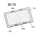
- 17A to 17D are diagrams for explaining an application example of the display device.
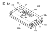
- 18A and 18B are diagrams for explaining an application example of the display device.
- FIG. 19 is a block diagram illustrating an example of a television device.
- FIG. 20 is a diagram illustrating a configuration example of a display panel.
- FIG. 21 is a diagram illustrating a configuration example of a display panel.
- FIG. 22 is a diagram illustrating a configuration example of the display panel.
- FIG. 23A is a block diagram of the display panel.
- 23B and 23C are circuit diagrams of pixels.
- 24A, 24C, and 24D are circuit diagrams of pixels.
- FIG. 24B is a timing chart illustrating the operation of the pixels.
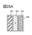
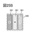
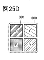
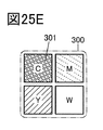
- 25A to 25E are diagrams for explaining a pixel configuration example.
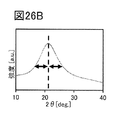
- FIG. 26A is a diagram illustrating the classification of the crystal structure of IGZO.
- FIG. 26B is a diagram illustrating an XRD spectrum of quartz glass.
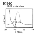
- FIG. 26C is a diagram illustrating an XRD spectrum of crystalline IGZO.
- FIG. 26D is a diagram illustrating a microelectron diffraction pattern of crystalline IGZO.
- 27A to 27D are cross-sectional views of the light emitting device.
- 28A to 28C are conceptual diagrams illustrating a light emitting model of the light emitting device.
- FIG. 28D is a diagram illustrating the normalized brightness of the light emitting device over time.
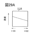
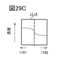
- 29A to 29D are diagrams illustrating the concentration of the organometallic complex in the electron transport layer.
- the element may be composed of a plurality of elements as long as there is no functional inconvenience.
- a plurality of transistors operating as switches may be connected in series or in parallel.
- the capacitor may be divided and arranged at a plurality of positions.
- one conductor may have a plurality of functions such as wiring, electrodes, and terminals, and in the present specification, a plurality of names may be used for the same element. Further, even if the elements are shown to be directly connected on the circuit diagram, the elements may actually be connected via one or a plurality of conductors. , In the present specification, such a configuration is also included in the category of direct connection.
- the display device refers to all devices having a function of displaying. That is, an electronic device having a display unit is included in the display device.
- an electronic device having a display unit such as a mobile phone, a smartphone, a smart watch, a tablet computer, or a television device is included in the display device.
- One aspect of the present invention is a display device that has a flexible display panel and can be folded into a small size.
- the display device has a tri-folding mechanism, and includes an area in which the first surfaces of the display device are folded so as to face each other and an area in which the second surface facing the first surface is folded so as to face each other. Can be formed. Therefore, even a display panel having a relatively large aspect ratio such as 16: 9, 18: 9, 21: 9 can be folded small by providing creases in the short axis direction, and portability can be improved. In addition, power consumption can be greatly reduced by hiding the invisible display area when folded into small pieces.
- FIG. 1A is a diagram showing a state in which the display device 100A of one aspect of the present invention is folded to the minimum size.
- the display device 100A can be deformed as shown in FIGS. 2A to 2C.
- the initial state is the folded state (see FIG. 2A)
- it can be brought into a flat unfolded state (see FIG. 2C) through a deformed state (see FIG. 2B). If you transform it in the reverse order, you can fold it.
- the display device 100A can be modified manually, but electrical power or mechanical power such as a spring may be used.
- the display device 100A includes a flexible display panel 101, a housing 102a, a housing 102b, a housing 102c, a hinge 103a, and a hinge 103b.
- the display panel 101 is divided into three regions, region 101a, region 101b, and region 101c, for the sake of clarity of explanation (see FIG. 2C).
- the regions 101a, 101b, and 101c are regions that are located parallel to the horizontal direction (the direction in which the surface of the display panel 101 extends) to form a surface when the display panel 101 is expanded flat, and the hinges. Is an area bordered by the position where is provided or its vicinity. In reality, there is no structural difference between the regions 101a to 101c and their boundaries.
- a seamless and flexible display panel can be used as the display panel 101.
- FIG. 1B is a diagram corresponding to a cross section of A1-A2 shown in FIG. 1A.
- the housing 102a is connected to the housing 102b via a hinge 103a.
- the housing 102b is connected to the housing 102c via a hinge 103b.
- the display panel 101 is provided on the first surface side of the housings 102a to 102c. At least a part of the area 101a can be fixed to the housing 102a. At least a part of the area 101b can be fixed to the housing 102b. At least a part of the region 101c can be fixed to the housing 102c.
- the surface of the display panel 101 fixed to the housing is the non-display surface and the surface of the display panel 101 facing the housing is the display surface, as shown in FIGS. 1A and 1B, when folded.
- the non-display surfaces of the region 101a and the region 101b face each other, and a curved surface 104a having a convex display surface is formed from the region 101a to the region 101b.
- the curved surface 104a is a region formed by a part of the region 101a and a part of the region 101b.
- the display surfaces of the region 101b and the region 101c face each other, and a curved surface 104b having a concave display surface is formed from the region 101b to the region 101c.
- the curved surface 104b is a region formed by a part of the region 101b and a part of the region 101c.
- the distance to the center of curvature is defined as the radius of curvature with respect to the surface (display surface) of the curved surface, the radius of curvature of the curved surface 104a when the display panel 101 is folded to the minimum size is R1, and the radius of curvature of the curved surface 104b is R2. To do. At this time, it is preferable that R1> R2.
- R1 is the radius of curvature when the display surface is bent outward, and even if the thicknesses of the housings 102a and 102a are formed thin within an appropriate range, the value is relatively large and forms the curved surface 104a of the display panel 101. The stress on the part is small.
- R2 is the radius of curvature when the display surface is bent inward, and is a relatively small value regardless of the thickness of the housings 102b and 102c, and the stress applied to the portion forming the curved surface 104b of the display panel 101. Is easy to grow.
- R2 is the same as or greater than R1
- the stress applied to the curved surface 104b can be reduced and the reliability can be improved.
- R2 is increased, the overall thickness when folded increases, resulting in inferior portability.
- a display panel resistant to bending stress can be realized without impairing reliability.
- a display panel resistant to bending stress can be realized by using a transistor (hereinafter, OS transistor) having a metal oxide (oxide semiconductor) in a channel forming region in a pixel circuit.
- the metal oxide can be formed by a film forming method such as a sputtering method, and can be produced by a relatively low temperature process. Therefore, there is little residual stress in devices such as transistors and peripheral members such as protective films, and it has strong resistance to bending stress applied later.
- examples of the transistor having the same level of electrical characteristics as the OS transistor include a transistor having silicon (low temperature polysilicon, single crystal silicon, etc.) in the channel forming region (hereinafter, Si transistor).
- Si transistor a transistor having silicon (low temperature polysilicon, single crystal silicon, etc.) in the channel forming region
- a laser crystallization step of a silicon film is used in the step of manufacturing a low-temperature polysilicon transistor.
- the temperature of the silicon film rises to a high temperature (at least the melting point of silicon) in the laser crystallization step for a short time, and the silicon film is rapidly cooled. Therefore, there is a large amount of residual stress on the silicon film and the peripheral members, and if bending stress is further applied later, the electrical characteristics and the like deteriorate, and the reliability is lowered.
- the display device of one aspect of the present invention it is easy to set R1> R2, and it can be folded into a small size without impairing reliability. Since the bending resistance varies depending on the radius of curvature, the number of times of bending, and the like, a Si tradista may be used in the pixel circuit depending on the situation.
- a metal oxide having an energy gap of 2 eV or more, preferably 2.5 eV or more, more preferably 3 eV or more can be used.
- a typical example is an oxide semiconductor containing indium, and for example, CAAC-OS or CAC-OS described later can be used.
- CAAC-OS is suitable for transistors and the like in which the atoms constituting the crystal are stable and reliability is important. Further, since CAC-OS exhibits high mobility characteristics, it is suitable for a transistor or the like that performs high-speed driving.
- the OS transistor Since the OS transistor has a large energy gap in the semiconductor layer, it can exhibit an extremely low off-current characteristic of several yA / ⁇ m (current value per 1 ⁇ m of channel width). Further, the OS transistor has features different from those of the Si transistor such as impact ionization, avalanche breakdown, and short channel effect, and can form a highly reliable circuit. In addition, variations in electrical characteristics due to crystallinity non-uniformity, which is a problem with Si transistors, are unlikely to occur with OS transistors.
- the semiconductor layer of the OS transistor is an In-M-Zn-based oxide containing, for example, indium, zinc and M (metals such as indium, titanium, gallium, germanium, ittrium, zirconium, lanthanum, cerium, tin, neodymium or hafnium). It can be a film represented by. Further, as the semiconductor layer of the OS transistor, an In oxide, an In—Ga oxide, or an In—Zn oxide may be used in addition to the In—M—Zn oxide. By using a semiconductor layer having a composition having a high proportion of indium, it is possible to increase the on-current of the OS transistor, the mobility of the field effect, and the like.
- the In-M-Zn-based oxide can be formed by, for example, a sputtering method, an ALD (Atomic layer deposition) method, a MOCVD (Metal organic chemical vapor deposition) method, or the like.
- the atomic number ratio of the metal element of the sputtering target preferably satisfies In ⁇ M and Zn ⁇ M.
- the oxide semiconductor constituting the semiconductor layer is In—Zn oxide
- the atomic number ratio of the metal element of the sputtering target used for forming the In—Zn oxide preferably satisfies In ⁇ Zn. ..
- the semiconductor layer an oxide semiconductor having a low carrier concentration is used.
- the semiconductor layer has a carrier concentration of 1 ⁇ 10 17 / cm 3 or less, preferably 1 ⁇ 10 15 / cm 3 or less, more preferably 1 ⁇ 10 13 / cm 3 or less, and more preferably 1 ⁇ 10 11 / cm. 3 or less, more preferably less than 1 ⁇ 10 10 / cm 3, it is possible to use an oxide semiconductor of 1 ⁇ 10 -9 / cm 3 or more carrier concentration.
- Such oxide semiconductors are referred to as high-purity intrinsic or substantially high-purity intrinsic oxide semiconductors. It can be said that the oxide semiconductor is an oxide semiconductor having a low defect level density and stable characteristics.
- a transistor having an appropriate composition may be used according to the required semiconductor characteristics and electrical characteristics (field effect mobility, threshold voltage, etc.) of the transistor. Further, in order to obtain the required semiconductor characteristics of the transistor, it is preferable that the carrier concentration, impurity concentration, defect density, atomic number ratio of metal element and oxygen, interatomic distance, density, etc. of the semiconductor layer are appropriate. ..
- the hinges 103a and 103b are abstracted and shown, and the form thereof does not matter. Specific examples of the hinges 103a and 103b will be described later, but elastic bodies such as rubber, connected columnar bodies, gears, and the like can be used. Although the housing and the hinge are shown as different elements in FIGS. 1A and 1B, the boundary is not clear and the housing and the hinge may be integrated. Further, the display panel 101 may not be in contact with the hinge.
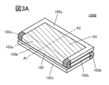
- one aspect of the present invention may have the configuration shown in FIG. 3A.
- the display device 100B shown in FIG. 3A has a configuration in which the hinge 103a of the display device 100A is replaced with the hinge 103c.
- the hinge 103c included in the display device 100B has a function of forming a curved surface 105a having a convex display surface, a flat surface 105, and a curved surface 105b having a convex display surface in this order from the region 101a to the region 101b when bent. ..
- the curved surface 105a is a region formed by a part of the region 101a
- the plane 105 is a region formed by a part of the region 101a and a part of the region 101b
- the curved surface 105b is formed by a part of the region 101c.
- R3> R2 and R4> R2 the radius of curvature of the curved surface 105a when folded to the minimum size
- R3> R2 and R4> R2 the overall thickness can be reduced as in the display device 100A.
- R3 and R4 are equal or substantially equal. By making R3 and R4 equal, it can be folded with good symmetry, and the reliability of the hinge mechanism can be improved. If R3 and R4 are significantly different, one of the region where the curved surface 105a is formed or the region where the curved surface 105b is formed becomes more easily bent than the other when folded or unfolded, which may impair reliability.
- the plane 105 is formed by the hinge 103c when bent. Therefore, the proportion of the flat surface in the bent portion is increased, and the visibility of the image can be improved.
- ⁇ Hinge> 4A to 4C are diagrams illustrating an example of a hinge 103a that can be used in the display device 100A shown in FIG. 1A.
- the hinge 103a has a plurality of columnar bodies 111 having a trapezoidal or substantially trapezoidal cross section in the minor axis direction.
- Each columnar body 111 is connected so that the bottom surface (corresponding to the lower bottom of the trapezoid) is continuous.
- the bottom surface of the columnar body 111 at one end of the hinge 103a is connected so as to be continuous with the first surface of the housing 102a.
- the bottom surface of the columnar body 111 at the other end of the hinge 103a is connected so as to be continuous with the first surface of the housing 102b.
- the shape of the upper surface (corresponding to the upper bottom of the trapezoid) of each columnar body 111 is arbitrary as long as it does not interfere with the other columnar bodies and the housing.
- the side surfaces (corresponding to trapezoidal legs) of adjacent columnar bodies 111 are deformed so as to be in contact with each other, so that the folded state can be obtained.
- the bottom surfaces of the plurality of columnar bodies 111 are connected at a constant angle, a region having a substantially arcuate cross section is formed as a whole. Therefore, the flexible display panel can form a curved surface at a portion overlapping the region.
- the cross section of the columnar body 111 is trapezoidal, but it may be triangular.
- the configuration for connecting each columnar body and the housing is not limited.
- a stopper may be provided to prevent bending in the direction opposite to the intended direction.
- a spacer may be provided to maintain a gap between the housings when folded.
- the housing or the hinge may be appropriately changed to a shape suitable for the installation of the display panel. These can also be applied to the hinge 103c described below.
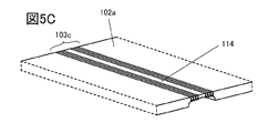
- 5A to 5C are diagrams illustrating an example of a hinge 103c that can be used in the display device 100B shown in FIG. 3A.
- the hinge 103c has units 113a, 113b having substantially the same elements as the hinge 103a.
- the units 113a and 113b may have a different number of columnar bodies from the hinge 103a.
- a columnar body 114 having a flat bottom surface and a side surface perpendicular to the bottom surface.
- the upper surface shape of the columnar body 114 is arbitrary as long as it does not interfere with other columnar bodies and the housing.
- the side surface of the columnar body of the unit 113a and the side surface of the columnar body of the columnar bodies 114 and 113b are deformed so as to be in contact with each other, so that the folded state can be obtained.
- the bottom surfaces of the columnar bodies of the unit 113a are connected at a constant angle, a region having a substantially arcuate cross section is formed.
- the flexible display panel can form a curved surface, a flat surface, or a curved surface at a portion overlapping the region.
- the columnar body of the unit 113a and the columnar body of the columnar body 114 and the unit 113b are connected so that the bottom surfaces are continuous. Further, the bottom surface of the columnar body at one end of the unit 113a is connected so as to be continuous with the first surface of the housing 102a. Further, the bottom surface of the columnar body at one end of the unit 113b is connected so as to be continuous with the first surface of the housing 102b.
- the first surface of the housing 102a, the bottom surface of the columnar body of the unit 113a, the bottom surface of the columnar body 114, and the columnar body of the unit 113b are connected so as to be flat.
- the curved surface of the display panel changes to a flat surface, and the display panel is developed flat as a whole. It can be folded by performing the deformation operation in the reverse order of the above.
- FIG. 6A to 6C are diagrams illustrating an example of a hinge 103b that can be used for the display device 100A shown in FIG. 1A or the display device 100B shown in FIG. 3A.
- the hinge 103b has a plurality of columnar bodies 115 having a rectangular cross section in the minor axis direction. Each columnar body 115 is connected so that the bottom surface is continuous. Further, the bottom surface of the columnar body 115 at one end of the hinge 103b is connected so as to be continuous with the first surface of the housing 102a. Further, the bottom surface of the columnar body 115 at the other end of the hinge 103b is connected so as to be continuous with the first surface of the housing 102c.
- the shape of the upper surface of each columnar body 115 is arbitrary as long as it does not interfere with the other columnar bodies and the housing.
- the folded state can be obtained by deforming the side surfaces of the adjacent columnar bodies 115 in the direction in which they are separated from each other. At this time, since the bottom surfaces of the plurality of columnar bodies 115 are connected at a constant angle, a region having a substantially arcuate cross section is formed as a whole. Therefore, the flexible display panel can form a curved surface at a portion overlapping the region.
- the first surface of the housing 102b, the bottom surface of each columnar body 115, and the first surface of the housing 102c become flat.
- the curved surface portion of the display panel also changes to be flat, and is in a state of being developed flat as a whole. It can be folded by performing the deformation operation in the reverse order of the above.
- the hinge 103b does not cause the display panel to bend in the opposite direction, and the stopper can be eliminated.
- a spacer may be provided to maintain a gap between the housings when folded. Further, the housing or the hinge may be appropriately deformed into a shape suitable for installing the display panel.
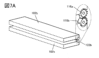
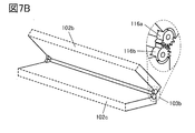
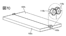
- FIG. 7A-7C are views illustrating another example of the hinge 103b.
- the hinge 103b has a gear 116a and a gear 116b.
- the gear 116a is fixed to the housing 102a.
- the gear 116b is fixed to the housing 102b.
- the central axis of the gear 116a preferably overlaps the first surface of the housing 102a. Further, it is preferable that the central axis of the gear 116b overlaps with the first surface of the housing 102b.
- the flexible display panel can form a curved surface having a radius of curvature of about 1/2 of the gap.
- the housing 102b and the housing 102c are synchronized according to the meshing of the gears 116a and 116b, and move so as to open with the hinge 103b as a fulcrum (FIG. 7B). reference).
- the radius of curvature of the curved surface portion changes so as to increase.
- the first surface of the housing 102b and the first surface of the housing 102c are connected so as to be flat.
- the curved surface of the display panel changes to a flat surface, and the display panel is developed flat as a whole. It can be folded by performing the deformation operation in the reverse order of the above.
- a mechanism for holding the meshing of the gear 116a and the gear 116b may be provided. Further, when deployed flat, the side surface of the housing 102c and the side surface of the housing 102c come into contact with each other. Therefore, the hinge 103b does not cause the display panel to bend in the opposite direction, and the stopper can be eliminated.
- a spacer may be provided to maintain a gap between the housings when folded. Alternatively, a mechanism for maintaining the gap may be provided in the gear 116a and the gear 116b. Further, the housing or the hinge may be appropriately deformed into a shape suitable for installing the display panel.
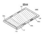
- FIG. 8A is a diagram illustrating a display device 100C which is a modification of the display device 100A.
- the shape of the housing 102c of the display device 100C is different from that of the display device 100A.
- the housing 102c included in the display device 100C is formed to be thicker than the housing 102a and the housing 102b. As shown in FIG. 8B, by forming the housing 102c thickly, a relatively large battery 117 can be contained therein, and the display device can be operated for a long time. Further, by incorporating the relatively heavy battery 117 in the housing 102c, the position of the center of gravity of the display device 100C can be set inside the housing 102c not only in the state of FIG. 8A but also in the state of FIG. 8B. .. Due to the thickness of the housing 102c and the center of gravity inside the housing 102c, it is possible to improve the ease of holding the display device when it is deployed flat.
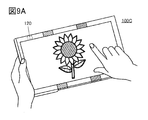
- FIG. 9A is a diagram showing a case where the housing 102c side of the display device 100C is held by the left hand and the screen touch operation is performed by the right hand.
- FIG. 9B is a diagram showing a case where the housing 102c side of the display device 100C is held by the right hand and the screen touch operation is performed by the left hand. In either case, the image can be displayed in an orientation that is easy for the user to see.
- This operation is performed by detecting the inclination of the display device 100C with a sensor 120 (acceleration sensor, gyro sensor, etc.) included in the display device 100C, and determining the orientation of the image display from the inclination. Further, the sensor 120 can detect the shaking of the display device 100C from the change in inclination. Since there are individual differences in shaking, it is possible to make the user judge by learning the shaking information with artificial intelligence (AI). Personal authentication can also be performed using this function.
- the sensor 120 can also be provided in other display devices shown in the present embodiment.
- FIG. 10 is a flowchart for determining the orientation of the displayed image and performing personal authentication using the sensor 120.
- the path from S1 to S2 is an operation of determining the orientation of the image display by using the tilt detection result of the sensor.
- the inclination has a plurality of directions, and the inclination A, the inclination B, and the inclination C include the conditions of the inclination in the plurality of directions.
- the inclination A is the range including the inclination of the display device 100C shown in FIG. 9A
- the inclination C is the range including the inclination of the display device 100C shown in FIG. 9B
- the inclination B is the longitudinal direction of the display device 100C.
- the range includes the inclination of time. Since there are two types of inclination B that are upside down, it is possible to actually make a judgment on four inclination ranges.
- A is displayed.
- the A display is a mode in which an image is displayed in the direction shown in FIG. 9A.
- C display is performed.
- the C display is a mode in which an image is displayed in the orientation shown in FIG. 9B.
- B display is performed.
- the B display is, for example, a mode in which the image of the display device 100C shown in FIG. 9A is rotated by approximately 90 degrees and displayed. In this way, the sensor 120 can be used to change the orientation of the image so that it can be easily viewed.
- the path of S1, S3, and S4 is an operation of accumulating the shaking data detected by the sensor 120 and registering the data and the individual.
- the data registered here is data for identifying an individual. The data can be updated each time the display device is used.
- the route passing through S1, S5, and S6 is an operation of collating the above data with the data related to the shaking output from the sensor 120 in real time to authenticate the individual.
- artificial intelligence AI which is deep learning of individual accumulated data on shaking
- the operation can be performed after the personal information is stored in the database. In this way, personal authentication can be performed using the sensor 120.
- the orientation of the display device 100c that the individual prefers to use can be known, so that the default display orientation can be set in advance.
- the sensor 120 may react sensitively due to a slight shaking of the display device 100C or the like. In this situation, it may take some time before the image can be visually recognized normally, such as the image being frequently rotated. In addition, wasteful power is consumed.
- the display orientation By setting the display orientation by default, the time required for visual recognition can be shortened and the power consumption can be reduced.
- the A display can be the default.
- the C display can be the default. It should be noted that the operation using the sensor 120 may be performed without using the function.
- FIG. 8C and 8D are views for explaining the display device 100D in which the battery is embedded in the housing 102a.
- the display device 100D has a grip portion 106 that is easy to grip at the end of the housing 102a, and the battery 117 can be embedded in the grip portion 106. Since the center of gravity of the display device 100D is located at the grip portion 106 containing the heavy battery 117, the ease of holding can be improved. Further, as shown in FIG. 8D, when the grip portion is deployed flat, the grip portion serves as a leg and can be used in a stable form even on a desk. In addition, since the display surface is slanted, visibility can be improved.
- the battery 117 is provided with the protection circuit 118.
- the battery 117 it is preferable to use a lithium ion battery capable of increasing the capacity, but in rare cases, an abnormality (micro short circuit or the like) inside the battery may cause a fire accident.
- the protection circuit 118 can be configured to include a comparator 121, a transistor 122, and a capacitor 123.
- the comparator 121 compares the voltage (V bat ) of the battery 117 with, for example, the reference potential (V ref ) which is the lower limit of the normal value, and outputs from the output terminal (OUT) when the V bat falls below the V ref. Invert the value.
- the V ref can be written and held in the node N to which one of the input terminals of the transistor 122, the capacitor 123 and the comparator 121 is connected.
- a circuit in which the transistor 122 and the capacitor 123 are combined is used as a memory circuit or a DOSRAM (Dynamic Oxide Semiconductor). It can be called a Random Access Memory). Since the DOSRAM can be composed of one transistor and one capacitance, it is possible to realize a high density of the memory. Further, by using the OS transistor, the data retention period can be increased.
- DOSRAM Dynamic Oxide Semiconductor
- the V ref is rewritten at regular intervals according to a change in voltage due to charging / discharging of the battery 117.
- the protection circuit 118 it is preferable to use an OS transistor for the transistor 122.
- the OS transistor has a low off current and can hold the potential written to the node N for a long time with substantially no fluctuation.
- the protection circuit 118 including the memory circuit may be referred to as a BTOS (Battery operating system or Battery oxide semiconductor).
- the battery 117 is electrically connected to the protection circuit 118, and the output of the protection circuit 118 is connected to the control circuit 119.
- the protection circuit 118 inverts the logical value of the signal output to the control circuit 119 when it detects a sudden voltage drop of the battery 117 or the like.
- the control circuit 119 controls the battery 117 to shut off charging and discharging to ensure the safety of the user.
- the antenna 125 is a 4th generation mobile communication system (4G) communication antenna
- the antenna 126 is a 5th generation mobile communication system (5G) communication antenna.
- 5G communication can perform high-speed communication 10 to 20 times faster than 4G communication.
- FIG. 8B and FIG. 8D the configuration in which both the antenna 125 and the antenna 126 are provided has been illustrated, but the present invention is not limited to this.
- the housing 102a may be configured to have only the antenna 125 or only the antenna 126.
- FIGS. 8B and 8D a configuration in which one antenna 125 and one antenna 126 are provided is illustrated, but the present invention is not limited to this.
- a plurality of antennas 125 may be provided, or a plurality of antennas 126 may be provided.
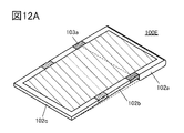
- FIGS. 8A and 8B an example in which the shape of the housing 102c is made thicker than other housings and a battery or the like is embedded is shown, but as in the display device 100E shown in FIG. 12A, the housing 102a The shape may be thicker than other housings.
- the hinge 103a corresponding to the outer bending can be appropriately bent so that the hinge 103a can be installed on a desk or the like in a well-balanced manner.
- the flat surface portion of the display surface can be divided into two with the hinge 103a as a boundary, an appropriate image can be assigned to each flat surface portion when displaying a plurality of images, and visibility is improved. Can be made to. It is also possible to hide one of the flat surface portions to perform a power saving operation.
- the housing 102c of the display device 100C may be further provided with a power receiving coil 107, a power receiving circuit 108, and the like. Wireless charging can be performed by overlapping the power receiving coil 107 and the power transmission coil of the charger 109.
- the housing 102c having a center of gravity can be placed in contact with the charger 109. Therefore, as shown in FIG. 12B, it can be stably placed on the charger 109 even when it is not folded. In addition, it can be used without impairing visibility even during charging.
- the power receiving coil 107 can be provided in all of the housings 102a, 102b, and 102c, any two, or any one.
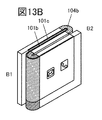
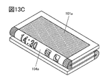
- FIGS. 13A to 13C are diagrams for explaining an operation example common to the display devices 100A to 100E of one aspect of the present invention.
- 13A to 13C show a case where the display device 100A is typically used.
- FIG. 13A is an operation in which the curved surface 104a is hidden when the flat surface portion of the region 101a is in the displayed state in the folded state.
- the folded and invisible regions region 101b including the curved surface 104b and region 101c are also hidden.
- the curved surface 104a may be in the display state.
- the folded and invisible area is also hidden. In this way, in the folded state, the power saving operation can be performed by displaying only a part of the area.
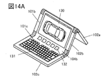
- ⁇ Display operation example 2> 14A to 14C are diagrams showing an example of a case where the display unit of the display devices 100A to 100D according to one aspect of the present invention is divided into three surfaces and used.
- FIG. 14A is a diagram showing an example in which the angle formed by the housing 102c and the housing 102b is an obtuse angle and the angle formed by the housing 102b and the housing 102a is an acute angle so that the housing 102b and the housing 102a are installed in a well-balanced manner on the desk.
- the housing 102a By using the housing 102a as a leg, it can be used like a laptop computer.
- the keyboard 131 is displayed on the area 101c
- the icon 132 is displayed on the curved surface 104b
- the image 130 of the application software is displayed on the area 101b, and the operation can be performed by touching the screen.
- the area 101a may be hidden and operated in the power saving mode.
- ⁇ Display operation example 3> 15A to 15C are diagrams showing an example of a case where the display unit of the display devices 100A to 100E according to one aspect of the present invention is used by being divided into two surfaces.
- the angle formed by the housing 102a and the housing 102b is approximately 60 ° or more and less than 180 ° (for example, about 90 °), and the angle formed by the housing 102b and the housing 102c is approximately 180 °.
- FIG. 15A It is a figure which shows an example of installing it on a desk in a well-balanced manner. Visibility can be improved by enlarging the screen as a continuous flat surface of the area 101b and the area 101c, and by inclining the display surface (area 101b and the area 101c) with the housing 102a as a leg.
- the area 101a may be hidden and operated in the power saving mode.
- the angle formed by the housing 102c and the housing 102b is smaller than approximately 180 ° and 90 ° or more (for example, about 135 °), and the angle formed by the housing 102b and the housing 102a is approximately 180 °.
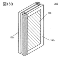
- 16A and 16B are diagrams showing an example in which the display device shown in the present embodiment is applied as an information terminal such as a smartphone.
- the same reference numerals are given to the elements common to the above-mentioned display devices.
- the display device 200 includes audio input / output units 135a and 135b, cameras 136a and 136b, a sensor 137, and a sensor 120.
- the audio input / output units 135a and 135b can be made to function as a speaker when one functions as a microphone. Therefore, when using the telephone function, it is possible to have a conversation without any inconvenience regardless of the orientation.
- the microphone function and the speaker function can be switched by the sensor 120 that detects the tilt. Further, the cameras 136a and 136b can also be made to function by giving priority to any of them by the sensor 120.
- the input / output units 135a and 135b may have both a device functioning as a microphone and a device functioning as a speaker, or may have one device having both functions.
- both the input / output units 135a and 135b can function as microphones to record stereo sound. Further, both the input / output units 135a and 135b can function as speakers to reproduce stereo sound.
- both cameras 136a and 136b can be operated to capture a 3D image.
- the sensor 137 is an optical sensor, and the brightness of the display can be adjusted so as to be easily visible according to the ambient illuminance.
- the display panel 138 may be provided on the rear surface opposite to the front surface on which the display panel 101 of the display device 200 is provided.
- the display panel 138 can display the same image as the display panel 101, and can also be used as a sub-display for displaying simple information, pictures, patterns, photographs, or the like, or as lighting.
- a display panel using a light emitting device or a liquid crystal device can be used, or low power consumption electronic paper or the like may be used.
- a display panel using a hard substrate as a support can also be used.
- the display panel 138 may be provided in each of the housings 102a to 102c.
- a flexible display panel 139 may be provided on the rear surface of the display device 200. In this case, since the display panel 139 can be bent, it can be provided over the housings 102a to 102c in the same manner as the display panel 101 provided on the front surface.
- the solar cell 140 may be provided on the rear surface of the display device 200.
- the electric power generated by the solar cell 140 can be charged to the battery in the display device 200, and can also be supplied to the outside through the external interface 145.
- FIG. 17C shows an example of a solar cell having a hard support.
- the solar cell for example, a silicon solar cell having crystalline silicon as a photoelectric conversion layer, or a solar cell having a silicon solar cell and a perovskite type solar cell having a tandem structure can be used.
- the solar cell may have a flexible substrate as a support.
- the solar cell for example, an amorphous silicon solar cell, a CIGS (Cu-In-Ga-Se) type solar cell, an organic solar cell, or a thin film solar cell 141 such as a perovskite type solar cell can be used. .. Similar to the display panel 139, the solar cell having the flexible substrate as a support can be provided over the housings 102a to 102c.
- 18A and 18B are diagrams showing an example of a case where the display units of the display devices 100A to 100D according to one aspect of the present invention are used properly according to the intended use.
- the display device 210 includes a transmission / reception unit 146, a speaker 147, a camera 148, a microphone 149, and the like.
- the display device 210 may have a function of a general tablet computer in addition to the function of one aspect of the present invention.
- the normal state it can be in a folded state as shown in FIG. 18A, and the clerk's calling function and the intercom function can be used.
- a menu is displayed and you can place an order.
- the order contents can be transmitted via the transmission / reception unit 146.
- payment can be made by displaying the total amount of orders or using a barcode captured by the camera 148.
- FIG. 19 is a block diagram showing an example in which the display device shown in the present embodiment is applied as a television device.
- FIG. 19 the components are classified by function and blocks that are independent of each other are shown. However, it is difficult to completely separate the actual components for each function, and one component can be divided into a plurality of functions. It can be involved.
- the television device 600 includes a control unit 601, a storage unit 602, a communication control unit 603, an image processing circuit 604, a decoder circuit 605, a video signal receiving unit 606, a timing controller 607, a source driver 608, a gate driver 609, a display panel 620, and the like.
- a control unit 601 a storage unit 602, a communication control unit 603, an image processing circuit 604, a decoder circuit 605, a video signal receiving unit 606, a timing controller 607, a source driver 608, a gate driver 609, a display panel 620, and the like.
- the display panel 620 corresponds to the display panel 101 shown in the first embodiment, and other elements can be contained in any of the housings 102a to 102c. Note that some elements such as the source driver 608 and the gate driver 609 may be elements of the display panel 101.
- the control unit 601 can function as, for example, a central processing unit (CPU: Central Processing Unit).
- CPU Central Processing Unit
- the control unit 601 has a function of controlling components such as a storage unit 602, a communication control unit 603, an image processing circuit 604, a decoder circuit 605, and a video signal receiving unit 606 via a system bus 630.
- control unit 601 Signals are transmitted between the control unit 601 and each component via the system bus 630. Further, the control unit 601 has a function of processing a signal input from each component connected via the system bus 630, a function of generating a signal output to each component, and the like, thereby being connected to the system bus 630. Each component can be controlled collectively.
- the storage unit 602 functions as a register, a cache memory, a main memory, a secondary memory, and the like that can be accessed by the control unit 601 and the image processing circuit 604.
- a storage device to which a rewritable non-volatile memory is applied can be used.
- flash memory MRAM (Magnetoresistive Random Access Memory), PRAM (Phasechange RAM), ReRAM (Resistive RAM), FeRAM (Ferroelectric RAM) and the like can be used.
- MRAM Magneticoresistive Random Access Memory
- PRAM Phasechange RAM
- ReRAM Resistive RAM
- FeRAM Feroelectric RAM
- a storage device that can be used as a temporary memory such as a register, a cache memory, and a main memory
- a volatile memory such as a DRAM (Dynamic RAM) or a SRAM (Static Random Access Memory) may be used.
- the RAM provided in the main memory for example, a DRAM is used, and a memory space is virtually allocated and used as a work space of the control unit 601.
- the operating system, application program, program module, program data, and the like stored in the storage unit 602 are loaded into the RAM for execution. These data, programs, and program modules loaded in the RAM are directly accessed and operated by the control unit 601.
- the ROM can store a BIOS (Basic Input / Output System), firmware, and the like that do not require rewriting.
- BIOS Basic Input / Output System
- a mask ROM an OTPROM (One Time Program Read Only Memory), an EPROM (Erasable Program Read Only Memory), or the like can be used.
- EPROM include UV-EPROM (Ultra-Violet Erasable Program Read Only Memory), EEPROM (Electrically Erasable Program Memory), etc., which enable erasure of stored data by irradiation with ultraviolet rays.
- a removable storage device may be connected.
- a recording medium drive such as a hard disk drive (Hard Disk Drive: HDD) or a solid state drive (Solid State Drive: SSD) that functions as a storage device, a flash memory, a Blu-ray disk, or a recording medium such as a DVD.
- HDD Hard Disk Drive
- SSD Solid State Drive
- the video can be recorded.
- the communication control unit 603 has a function of controlling communication performed via a computer network. That is, the technology of IoT (Internet of Things) is applied to the television device 600.
- IoT Internet of Things
- the communication control unit 603 controls, for example, a control signal for connecting to the computer network in response to a command from the control unit 601 and transmits the signal to the computer network.
- the Internet Intranet, Extranet, PAN (Personal Area Network), LAN (Local Area Network), CAN (Campus Area Network), MAN (Monet), which are the foundations of the World Wide Web (WWW) It is possible to connect to a computer network such as Wide Area Network) and GAN (Global Area Network) and perform communication.
- the communication control unit 603 has a function of communicating with a computer network or other electronic devices using communication standards such as Wi-Fi (registered trademark), Bluetooth (registered trademark), and ZigBee (registered trademark). May be good.
- Wi-Fi registered trademark
- Bluetooth registered trademark
- ZigBee registered trademark
- the communication control unit 603 may have a function of wirelessly communicating.
- an antenna and a high frequency circuit RF circuit
- the high-frequency circuit is a circuit for mutually converting an electromagnetic signal and an electric signal in a frequency band defined by the legislation of each country and wirelessly communicating with another communication device using the electromagnetic signal. Several tens of kHz to several tens of GHz are generally used as a practical frequency band.
- the high-frequency circuit connected to the antenna may have a high-frequency circuit section corresponding to a plurality of frequency bands, and the high-frequency circuit section may have an amplifier, a mixer, a filter, a DSP, an RF transceiver, and the like. it can.
- the video signal receiving unit 606 includes, for example, an antenna, a demodulation circuit, an AD conversion circuit (analog-digital conversion circuit), and the like.
- the demodulation circuit has a function of demodulating the signal input from the antenna.
- the AD conversion circuit has a function of converting the demodulated analog signal into a digital signal.
- the signal processed by the video signal receiving unit 606 is sent to the decoder circuit 605.
- the decoder circuit 605 has a function of decoding the video data included in the digital signal input from the video signal receiving unit 606 according to the specifications of the broadcasting standard to be transmitted and generating a signal to be transmitted to the image processing circuit.
- the broadcasting standard in 8K broadcasting
- Examples of the broadcast radio wave that can be received by the antenna included in the video signal receiving unit 606 include terrestrial waves and radio waves transmitted from satellites. Broadcasting radio waves that can be received by the antenna include analog broadcasting, digital broadcasting, and video and audio, or audio-only broadcasting. For example, it is possible to receive broadcast radio waves transmitted in a specific frequency band within the UHF band (about 300 MHz to 3 GHz) or the VHF band (30 MHz to 300 MHz). Further, for example, by using a plurality of data received in a plurality of frequency bands, the transfer rate can be increased and more information can be obtained. As a result, an image having a resolution exceeding full high definition can be displayed on the display panel 620. For example, it is possible to display an image having a resolution of 4K2K, 8K4K, 16K8K, or higher.
- the video signal receiving unit 606 and the decoder circuit 605 may be configured to generate a signal to be transmitted to the image processing circuit 604 by using the broadcast data transmitted by the data transmission technology via the computer network. At this time, if the signal to be received is a digital signal, the video signal receiving unit 606 does not have to have a demodulation circuit, an AD conversion circuit, or the like.
- the image processing circuit 604 has a function of generating a video signal to be output to the timing controller 607 based on the video signal input from the decoder circuit 605.
- the timing controller 607 generates signals (clock signals, start pulse signals, and other signals) to be output to the gate driver 609 and the source driver 608 based on the synchronization signal included in the video signal or the like processed by the image processing circuit 604. Has the function of Further, the timing controller 607 has a function of generating a video signal to be output to the source driver 608 in addition to the above signal.
- the display panel 620 has a plurality of pixels 621. Each pixel 621 is driven by signals supplied by the gate driver 609 and the source driver 608.
- a display panel having a pixel count of 7680 ⁇ 4320 and a resolution corresponding to the 8K4K standard is shown.
- the resolution of the display panel 620 is not limited to this, and may be a resolution according to a standard such as full high-definition (number of pixels 1920 ⁇ 1080) or 4K2K (number of pixels 3840 ⁇ 2160).
- the control unit 601 and the image processing circuit 604 shown in FIG. 19 may have, for example, a processor.
- the control unit 601 can use a processor that functions as a CPU.
- the image processing circuit 604 for example, another processor such as a DSP (Digital Signal Processor) or a GPU (Graphics Processing Unit) can be used.
- the control unit 601 and the image processing circuit 604 may be configured such that the processor is realized by a PLD (Programmable Logic Device) such as FPGA (Field Programmable Gate Array) or FPGA (Field Programmable Analog Array).
- PLD Programmable Logic Device
- FPGA Field Programmable Gate Array
- FPGA Field Programmable Analog Array
- the processor performs various data processing and program control by interpreting and executing instructions from various programs.
- the program that can be executed by the processor may be stored in a memory area of the processor, or may be stored in a storage device provided separately.
- a system LSI may be configured by consolidating them into one IC chip.
- it may be a system LSI having a processor, a decoder circuit, a tuner circuit, an AD conversion circuit, a DRAM, an SRAM, and the like.
- a transistor in which an oxide semiconductor is used in the channel forming region and an extremely low off-current is realized can also be used for the control unit 601 and the IC and the like possessed by other components. Since the transistor has an extremely low off current, the data retention period can be secured for a long period of time by using the transistor as a switch for holding the electric charge (data) that has flowed into the capacitance that functions as a memory.
- the control unit 601 is operated only when necessary, and in other cases, the information of the immediately preceding process is saved in the memory, thereby normally off. Computing becomes possible. As a result, the power consumption of the television device 600 can be reduced.
- the configuration of the television device 600 in FIG. 19 is an example, and it is not necessary to include all the components.
- the television device 600 may have the necessary components among the components shown in FIG. Further, the television device 600 may have components other than the components shown in FIG.
- the television device 600 may have an external interface, an audio output unit, a touch panel unit, a sensor unit, a camera unit, and the like, in addition to the configuration shown in FIG.
- an external interface for example, a USB (Universal Serial Bus) terminal, a LAN (Local Area Network) connection terminal, a power receiving terminal, an audio output terminal, an audio input terminal, a video output terminal, a video input terminal, etc.
- a USB Universal Serial Bus
- LAN Local Area Network
- the audio input / output unit includes a sound controller, a microphone, a speaker, and the like.
- the image processing circuit 604 preferably has a function of executing image processing based on a video signal input from the decoder circuit 605.
- Examples of the image processing include noise removal processing, gradation conversion processing, color tone correction processing, and luminance correction processing.
- Examples of the color tone correction process and the brightness correction process include gamma correction.
- the image processing circuit 604 has a function of executing processing such as inter-pixel interpolation processing associated with resolution up-conversion and inter-frame interpolation processing associated with frame frequency up-conversion.
- noise removal processing various noises such as mosquito noise generated around contours such as characters, block noise generated in high-speed moving images, random noise causing flicker, and dot noise generated by up-conversion of resolution are removed.
- the gradation conversion process is a process of converting the gradation of an image into a gradation corresponding to the output characteristics of the display panel 620. For example, when increasing the number of gradations, it is possible to perform a process of smoothing the histogram by interpolating and assigning gradation values corresponding to each pixel to an image input with a small number of gradations. High dynamic range (HDR) processing that expands the dynamic range is also included in the gradation conversion processing.
- HDR High dynamic range
- the inter-pixel interpolation process interpolates data that does not originally exist when the resolution is up-converted. For example, the pixels around the target pixel are referenced, and the data is interpolated so as to display their intermediate colors.
- the color tone correction process is a process for correcting the color tone of an image.
- the brightness correction process is a process for correcting the brightness (luminance contrast) of an image. For example, the type and brightness of the illumination in the space where the television device 600 is provided, the color purity, and the like are detected, and the brightness and color tone of the image displayed on the display panel 620 are corrected accordingly. Alternatively, it has a function of collating the image to be displayed with the image of various scenes in the image list saved in advance and correcting the image to be displayed with the brightness and color tone suitable for the image of the closest scene. You may.
- Inter-frame interpolation generates an image of a frame (interpolation frame) that does not originally exist when the frame frequency of the image to be displayed is increased.
- an image of an interpolation frame to be inserted between two images is generated from the difference between two images.
- the frame frequency of the video signal input from the decoder circuit 605 is 60 Hz
- the frame frequency of the video signal output to the timing controller 607 is doubled to 120 Hz or 120 Hz by generating a plurality of interpolated frames. It can be increased to 4 times 240 Hz, 8 times 480 Hz, and the like.
- This embodiment can be implemented in combination with at least a part thereof as appropriate with other embodiments described in the present specification.
- FIG. 20 shows a top view of the display panel 700.
- the display panel 700 is a display panel to which a flexible support substrate 745 is applied and can be used as a flexible display. Further, the display panel 700 has a pixel portion 702 provided on the flexible support substrate 745. Further, a source driver circuit unit 704, a pair of gate driver circuit units 706, wiring 710, and the like are provided on the support board 745. Further, the pixel unit 702 is provided with a plurality of display devices.
- an FPC terminal portion 708 to which an FPC 716 (FPC: Flexible printed circuit board) is connected is provided as a part of the support substrate 745.
- FPC 716 Flexible printed circuit board
- Various signals and the like are supplied by the FPC 716 to the pixel unit 702, the source driver circuit unit 704, and the gate driver circuit unit 706 via the FPC terminal unit 708 and the wiring 710.
- a pair of gate driver circuit units 706 are provided on both sides of the pixel unit 702.
- the gate driver circuit unit 706 and the source driver circuit unit 704 may be in the form of an IC chip that is separately formed and packaged on a semiconductor substrate or the like.
- the IC chip can be mounted on a support substrate 745 by COF (Chip On Film) technology or the like.
- the OS transistor it is preferable to apply the OS transistor to the transistor included in the pixel unit 702, the source driver circuit unit 704, and the gate driver circuit unit 706.
- a light emitting device or the like can be used as the display device provided in the pixel unit 702.
- the light emitting device include self-luminous light emitting devices such as an LED (Light Emitting Diode), an OLED (Organic LED), a QLED (Quantum-dot LED), and a semiconductor laser.
- a liquid crystal device such as a transmissive liquid crystal device, a reflective liquid crystal device, or a semi-transmissive liquid crystal device can also be used.
- a shutter type or optical interference type MEMS (Micro Electroelectric Mechanical Systems) device a display device to which a microcapsule method, an electrophoresis method, an electrowetting method, an electronic powder fluid (registered trademark) method, or the like is applied is used. You can also do it.
- MEMS Micro Electroelectric Mechanical Systems
- FIG. 20 shows an example of the support substrate 745 in which the portion where the FPC terminal portion 708 is provided has a protruding shape.
- a part of the support substrate 745 including the FPC terminal portion 708 can be folded back in the region P1 in FIG. 20.
- the display panel 700 can be mounted on an electronic device or the like in a state where the FPC 716 is overlapped on the back side of the pixel portion 702, and the space and size of the electronic device or the like can be reduced. Can be planned.
- the IC 717 is mounted on the FPC 716 connected to the display panel 700.
- the IC717 has a function as, for example, a source driver circuit.
- the source driver circuit unit 704 in the display panel 700 can be configured to include at least one of a protection circuit, a buffer circuit, a demultiplexer circuit, and the like.
- FIGS. 21 and 22 are schematic cross-sectional views taken along the alternate long and short dash line ST of the display panel 700 shown in FIG. 20, respectively.
- 21 and 22 show a cross section including a pixel unit 702, a gate driver circuit unit 706, and an FPC terminal unit 708.
- the pixel unit 702 has a transistor 750 and a capacitor 790.
- the gate driver circuit unit 706 has a transistor 752.
- the transistor 750 and the transistor 752 are transistors in which an oxide semiconductor is applied to a semiconductor layer on which a channel is formed. Not limited to this, a transistor using silicon (amorphous silicon, polycrystalline silicon, or single crystal silicon) or an organic semiconductor can be applied to the semiconductor layer.
- the transistor used in this embodiment has an oxide semiconductor film that is highly purified and suppresses the formation of oxygen deficiency.
- the transistor can significantly reduce the off current. Therefore, the pixel to which such a transistor is applied can have a long holding time of an electric signal such as an image signal, and a long writing interval of the image signal or the like can be set. Therefore, the frequency of refresh operations can be reduced, and power consumption can be reduced.
- the transistor used in this embodiment can be driven at high speed because a relatively high field effect mobility can be obtained.
- a transistor capable of high-speed driving for the display panel it is possible to form the switching transistor of the pixel portion and the driver transistor used for the driving circuit portion on the same substrate. That is, a configuration in which a drive circuit formed of a silicon wafer or the like is not applied is also possible, and the number of parts of the display device can be reduced. Further, also in the pixel portion, it is possible to provide a high-quality image by using a transistor capable of high-speed driving.
- the capacitor 790 has a lower electrode formed by processing the same film as the first gate electrode of the transistor 750, and an upper electrode formed by processing the same metal oxide film as the semiconductor layer. ..
- the upper electrode has a low resistance as in the source region and drain region of the transistor 750. Further, a part of an insulating film that functions as a first gate insulating layer of the transistor 750 is provided between the lower electrode and the upper electrode. That is, the capacitor 790 has a laminated structure in which an insulating film functioning as a dielectric film is sandwiched between a pair of electrodes. Further, a wiring obtained by processing the same film as the source electrode and the drain electrode of the transistor 750 is connected to the upper electrode.
- an insulating layer 770 that functions as a flattening film is provided on the transistor 750, the transistor 752, and the capacitor 790.
- the transistor 750 included in the pixel unit 702 and the transistor 752 included in the gate driver circuit unit 706 may use transistors having different structures. For example, a top gate type transistor may be applied to either one, and a bottom gate type transistor may be applied to the other.
- the source driver circuit unit 704 is the same as the gate driver circuit unit 706.
- the FPC terminal portion 708 has a wiring 760, an anisotropic conductive film 780, and an FPC 716, which partially function as connection electrodes.
- the wiring 760 is electrically connected to the terminal of the FPC 716 via the anisotropic conductive film 780.
- the wiring 760 is formed of the same conductive film as the source electrode and the drain electrode of the transistor 750 and the like.
- the display panel 700 shown in FIG. 21 has a support substrate 745 and a support substrate 740.
- a flexible substrate such as a glass substrate or a plastic substrate can be used.
- the transistor 750, the transistor 752, the capacitor 790, and the like are provided on the insulating layer 744.
- the support substrate 745 and the insulating layer 744 are bonded to each other by the adhesive layer 742.
- the display panel 700 has a light emitting device 782, a colored layer 736, a light shielding layer 738, and the like.
- the light emitting device 782 has a conductive layer 772, an EL layer 786, and a conductive layer 788.
- the conductive layer 772 is electrically connected to the source electrode or drain electrode of the transistor 750.
- the conductive layer 772 is provided on the insulating layer 770 and functions as a pixel electrode. Further, an insulating layer 730 is provided so as to cover the end portion of the conductive layer 772, and an EL layer 786 and a conductive layer 788 are laminated on the insulating layer 730 and the conductive layer 772.
- the light emitting device 782 is a top emission type light emitting device that emits light to the side opposite to the surface to be formed (support substrate 740 side).
- the EL layer 786 has an organic compound or an inorganic compound such as a quantum dot.
- the EL layer 786 contains a light emitting material that exhibits blue light when an electric current flows through it.
- a fluorescent material As the light emitting material, a fluorescent material, a phosphorescent material, a thermally activated delayed fluorescence (TADF) material, an inorganic compound (quantum dot material, etc.) and the like can be used.
- TADF thermally activated delayed fluorescence
- quantum dot material an inorganic compound
- examples of materials that can be used for quantum dots include colloidal quantum dot materials, alloy-type quantum dot materials, core-shell type quantum dot materials, and core-type quantum dot materials.
- the light-shielding layer 738 and the colored layer 736 are provided on one surface of the insulating layer 746.
- the colored layer 736 is provided at a position overlapping the light emitting device 782.
- the light-shielding layer 738 is provided in the pixel portion 702 in a region that does not overlap with the light emitting device 782. Further, the light-shielding layer 738 may be provided so as to be overlapped with the gate driver circuit unit 706 or the like.
- the support substrate 740 is bonded to the other surface of the insulating layer 746 by an adhesive layer 747. Further, the support substrate 740 and the support substrate 745 are bonded to each other by the sealing layer 732.
- the EL layer 786 of the light emitting device 782 a light emitting material exhibiting white light emission is applied.
- the white light emitted by the light emitting device 782 is colored by the colored layer 736 and emitted to the outside.
- the EL layer 786 is provided over pixels that exhibit different colors. By arranging pixels provided with a colored layer 736 that transmits any of red (R), green (G), and blue (B) in a matrix in the pixel portion, the display panel 700 can be made full-color. Can be displayed.
- a conductive film having semi-transmissive and semi-reflective properties may be used as the conductive layer 788.
- a microcavity structure can be realized between the conductive layer 772 and the conductive layer 788, and the light having a specific wavelength can be strengthened and emitted.
- an optical adjustment layer for adjusting the optical distance is arranged between the conductive layer 772 and the conductive layer 788, and the thickness of the optical adjustment layer is made different between pixels of different colors. It may be configured to increase the color purity of the light emitted from the pixel.
- the colored layer 736 or the above-mentioned optical adjustment layer may not be provided.
- the insulating layer 744 and the insulating layer 746 each use an inorganic insulating film that functions as a barrier film having low moisture permeability.
- a resin layer 743 is provided between the adhesive layer 742 and the insulating layer 744 shown in FIG. 21. Further, instead of the support substrate 740, the protective layer 749 is provided.
- the resin layer 743 is a layer containing an organic resin such as polyimide or acrylic.
- the insulating layer 744 includes an inorganic insulating film such as silicon oxide, silicon oxide nitride, or silicon nitride.
- the resin layer 743 and the support substrate 745 are attached to each other by the adhesive layer 742.
- the resin layer 743 is preferably thinner than the support substrate 745.
- the protective layer 749 is attached to the sealing layer 732.
- a glass substrate, a resin film, or the like can be used.
- an optical member such as a polarizing plate (including a circular polarizing plate) and a scattering plate, an input device such as a touch sensor panel, or a configuration in which two or more of these are laminated may be applied.
- the EL layer 786 of the light emitting device 782 is provided in an island shape on the insulating layer 730 and the conductive layer 772. By forming the EL layer 786 so that the emission color is different for each sub-pixel, color display can be realized without using the coloring layer 736.
- a protective layer 741 is provided so as to cover the light emitting device 782.
- the protective layer 741 has a function of preventing impurities such as water from diffusing into the light emitting device 782.
- the protective layer 741 has a laminated structure in which the insulating layer 741a, the insulating layer 741b, and the insulating layer 741c are laminated in this order from the conductive layer 788 side. At this time, it is preferable to use an inorganic insulating film having a high barrier property against impurities such as water for the insulating layer 741a and the insulating layer 741c, and an organic insulating film functioning as a flattening film for the insulating layer 741b. .. Further, the protective layer 741 is preferably provided so as to extend to the gate driver circuit unit 706.
- an organic insulating film covering the transistor 750, the transistor 752, and the like is formed in an island shape inside the sealing layer 732.
- the end portion of the organic insulating film is located inside the sealing layer 732 or in a region overlapping the end portion of the sealing layer 732.
- FIG. 22 shows an example in which the insulating layer 770, the insulating layer 730, and the insulating layer 741b are processed into an island shape.
- the insulating layer 741c and the insulating layer 741a are provided in contact with each other.
- the surface of the organic insulating film covering the transistor 750 and the transistor 752 is not exposed to the outside of the sealing layer 732, so that water is supplied to the transistor 750 and the transistor 752 from the outside via the organic insulating film. And hydrogen can be suitably prevented from diffusing. As a result, fluctuations in the electrical characteristics of the transistor can be suppressed, and a display device with extremely high reliability can be realized.
- the bendable region P1 has a portion in which an inorganic insulating film such as an insulating layer 744 is not provided in addition to the support substrate 745 and the adhesive layer 742. Further, in the region P1, in order to prevent the wiring 760 from being exposed, the insulating layer 770 containing an organic material covers the wiring 760. By forming a structure in which an inorganic insulating film is not provided as much as possible in the bendable region P1 and only a conductive layer containing a metal or an alloy and a layer containing an organic material are laminated, cracks are generated when bent. Can be prevented. Further, by not providing the support substrate 745 in the region P1, a part of the display panel 700A can be bent with an extremely small radius of curvature.
- a conductive layer 761 is provided on the protective layer 741.
- the conductive layer 761 can be used as wiring or electrodes.
- the conductive layer 761 functions as an electrostatic shielding film for preventing electrical noise when driving the pixels from being transmitted to the touch sensor. be able to.
- the conductive layer 761 may be configured to be provided with a predetermined constant potential.
- the conductive layer 761 can be used, for example, as an electrode of a touch sensor.
- the display panel 700A can function as a touch panel.
- the conductive layer 761 can be used as an electrode or wiring of a capacitance type touch sensor.
- the conductive layer 761 can be used as a wiring or electrode to which the detection circuit is connected or as a wiring or electrode to which the sensor signal is input.
- the conductive layer 761 is preferably provided at a portion that does not overlap with the light emitting device 782.
- the conductive layer 761 can be provided at a position overlapping the insulating layer 730.
- the touch sensor method that can be configured by using the conductive layer 761 is not limited to the capacitance method, but various methods such as a resistance film method, a surface acoustic wave method, an infrared method, an optical method, and a pressure sensitive method. Can be used. Alternatively, two or more of these may be used in combination.
- the transistor has a conductive layer that functions as a gate electrode, a semiconductor layer, a conductive layer that functions as a source electrode, a conductive layer that functions as a drain electrode, and an insulating layer that functions as a gate insulating layer.
- the structure of the transistor included in the display device of one aspect of the present invention is not particularly limited.
- it may be a planar type transistor, a stagger type transistor, or an inverted stagger type transistor.
- a top gate type or a bottom gate type transistor structure may be used.
- gate electrodes may be provided above and below the channel.
- the crystallinity of the semiconductor material used for the transistor is also not particularly limited, and either an amorphous semiconductor or a semiconductor having crystallinity (microcrystalline semiconductor, polycrystalline semiconductor, single crystal semiconductor, or semiconductor having a partially crystalline region). May be used. It is preferable to use a semiconductor having crystallinity because deterioration of transistor characteristics can be suppressed.
- ⁇ Conductive layer> Materials that can be used for conductive layers such as transistor gates, sources and drains, as well as various wiring and electrodes that make up display devices include aluminum, titanium, chromium, nickel, copper, yttrium, zirconium, molybdenum, and silver. Examples thereof include tantalum, metals such as tungsten, and alloys containing this as a main component. Further, a film containing these materials can be used as a single layer or as a laminated structure.
- a single-layer structure of an aluminum film containing silicon a two-layer structure in which an aluminum film is laminated on a titanium film, a two-layer structure in which an aluminum film is laminated on a tungsten film, and a copper film on a copper-magnesium-aluminum alloy film.
- Two-layer structure for laminating, two-layer structure for laminating copper film on titanium film, two-layer structure for laminating copper film on tungsten film, titanium film or titanium nitride film, and aluminum film or copper film on top of it A three-layer structure, a molybdenum film or a molybdenum nitride film, on which a titanium film or a titanium nitride film is formed, and an aluminum film or a copper film on which an aluminum film or a copper film is laminated, and then a molybdenum film or There is a three-layer structure for forming a molybdenum nitride film.
- Oxides such as indium oxide, tin oxide, and zinc oxide may be used. Further, it is preferable to use copper containing manganese because the controllability of the shape by etching is improved.
- Insulating materials that can be used for each insulating layer include, for example, resins such as acrylic and epoxy, resins having a siloxane bond, and inorganic insulation such as silicon oxide, silicon oxide nitride, silicon nitride oxide, silicon nitride, and aluminum oxide. Materials can also be used.
- the light emitting device is preferably provided between a pair of insulating films having low water permeability. As a result, impurities such as water can be suppressed from entering the light emitting device, and deterioration of the reliability of the device can be suppressed.
- the insulating film having low water permeability examples include a film containing nitrogen and silicon such as a silicon nitride film and a silicon nitride film, and a film containing nitrogen and aluminum such as an aluminum nitride film. Further, a silicon oxide film, a silicon nitride film, an aluminum oxide film or the like may be used.
- water vapor permeability of less water permeable insulating film 1 ⁇ 10 -5 [g / (m 2 ⁇ day)] or less, preferably 1 ⁇ 10 -6 [g / ( m 2 ⁇ day)] or less, It is more preferably 1 ⁇ 10 -7 [g / (m 2 ⁇ day)] or less, and further preferably 1 ⁇ 10 -8 [g / (m 2 ⁇ day)] or less.
- This embodiment can be implemented in combination with at least a part thereof as appropriate with other embodiments described in the present specification.
- the display device shown in FIG. 23A includes a pixel unit 502, a drive circuit unit 504, a protection circuit 506, and a terminal unit 507.
- the protection circuit 506 may not be provided.
- the pixel unit 502 has a plurality of pixel circuits 501 for driving a plurality of display devices arranged in X rows and Y columns (X and Y are independently two or more natural numbers).
- the drive circuit unit 504 has a drive circuit such as a gate driver 504a that outputs a scanning signal to the gate lines GL_1 to GL_X, and a source driver 504b that supplies a data signal to the data lines DL_1 to DL_Y.
- the gate driver 504a may be configured to have at least a shift register.
- the source driver 504b is configured by using, for example, a plurality of analog switches. Further, the source driver 504b may be configured by using a shift register or the like.
- the terminal portion 507 refers to a portion provided with a terminal for inputting a power supply, a control signal, an image signal, or the like from an external circuit to the display device.
- the protection circuit 506 is a circuit that makes the wiring and another wiring conductive when a potential outside a certain range is applied to the wiring to which the protection circuit 506 is connected.
- the protection circuit 506 shown in FIG. 23A is used for various wirings such as a gate line GL which is a wiring between the gate driver 504a and the pixel circuit 501 or a data line DL which is a wiring between the source driver 504b and the pixel circuit 501. Be connected.
- the gate driver 504a and the source driver 504b may be provided on the same substrate as the pixel portion 502, respectively, or a substrate on which a gate driver circuit or a source driver circuit is separately formed (for example, a single crystal semiconductor film or multiple substrates).
- a drive circuit board formed of a crystalline semiconductor film may be mounted on the board by COF, TCP (Tape Carrier Package), COG (Chip On Glass), or the like.
- the plurality of pixel circuits 501 shown in FIG. 23A can have the configuration shown in FIGS. 23B and 23C, for example.
- the pixel circuit 501 shown in FIG. 23B includes a liquid crystal device 570, a transistor 550, and a capacitor 560. Further, a data line DL_n, a gate line GL_m, a potential supply line VL, and the like are connected to the pixel circuit 501.
- the potential of one of the pair of electrodes of the liquid crystal device 570 is appropriately set according to the specifications of the pixel circuit 501.
- the orientation state of the liquid crystal device 570 is set according to the written data.
- a common potential (common potential) may be applied to one of the pair of electrodes of the liquid crystal device 570 of each of the plurality of pixel circuits 501. Further, different potentials may be applied to one of the pair of electrodes of the liquid crystal device 570 of the pixel circuit 501 of each row.
- the pixel circuit 501 shown in FIG. 23C includes transistors 552 and 554, a capacitor 562, and a light emitting device 527. Further, a data line DL_n, a gate line GL_m, a potential supply line VL_a, a potential supply line VL_b, and the like are connected to the pixel circuit 501.
- One of the potential supply line VL_a and the potential supply line VL_b is given a high power supply potential VDD, and the other is given a low power supply potential VSS.
- the brightness of light emitted from the light emitting device 572 is controlled by controlling the current flowing through the light emitting device 572 according to the potential given to the gate of the transistor 554.
- This embodiment can be implemented in combination with at least a part thereof as appropriate with other embodiments described in the present specification.
- FIG. 24A shows a circuit diagram of the pixel circuit 400.
- the pixel circuit 400 includes a transistor M1, a transistor M2, a capacitance C1, and a circuit 401. Further, wiring S1, wiring S2, wiring G1 and wiring G2 are connected to the pixel circuit 400.
- the gate is connected to the wiring G1
- one of the source and drain is connected to the wiring S1
- the other is connected to one electrode of the capacitance C1.
- the transistor M2 connects the gate to the wiring G2, one of the source and the drain to the wiring S2, the other to the other electrode of the capacitance C1, and the circuit 401, respectively.
- Circuit 401 is a circuit that includes at least one display device.
- Various devices can be used as the display device, and typically, a light emitting device such as an organic EL device or an LED device, a liquid crystal device, a MEMS (Micro Electro Mechanical Systems) device or the like can be applied.
- node N1 The node connecting the transistor M1 and the capacitance C1 is referred to as node N1, and the node connecting the transistor M2 and the circuit 401 is referred to as node N2.
- the pixel circuit 400 can hold the potential of the node N1 by turning off the transistor M1. Further, by turning off the transistor M2, the potential of the node N2 can be maintained. Further, by writing a predetermined potential to the node N1 via the transistor M1 with the transistor M2 turned off, the potential of the node N2 is corresponding to the displacement of the potential of the node N1 by capacitive coupling via the capacitance C1. Can be changed.
- the transistor to which the oxide semiconductor illustrated in the first embodiment is applied can be applied to one or both of the transistor M1 and the transistor M2. Therefore, the potential of the node N1 and the node N2 can be maintained for a long period of time due to the extremely low off current.
- a transistor to which a semiconductor such as silicon is applied may be used.
- FIG. 24B is a timing chart related to the operation of the pixel circuit 400.
- the effects of various resistors such as wiring resistance, parasitic capacitance of transistors and wiring, and threshold voltage of transistors are not considered here.
- one frame period is divided into a period T1 and a period T2.
- the period T1 is a period for writing the potential to the node N2
- the period T2 is a period for writing the potential to the node N1.
- both the wiring G1 and the wiring G2 are given a potential to turn on the transistor. Further, the potential V ref , which is a fixed potential, is supplied to the wiring S1, and the first data potential V w is supplied to the wiring S2.
- the potential V ref is given to the node N1 from the wiring S1 via the transistor M1. Further, the node N2 is given a first data potential V w from the wiring S2 via the transistor M2. Therefore, the capacitance C1 is in a state where the potential difference V w ⁇ V ref is held.
- the wiring G1 is given a potential for turning on the transistor M1, and the wiring G2 is given a potential for turning off the transistor M2. Further, a second data potential V data is supplied to the wiring S1.
- a predetermined constant potential may be applied to the wiring S2, or the wiring S2 may be floating.
- a second data potential V data is given to the node N1 from the wiring S1 via the transistor M1.
- the potential of the node N2 changes by the potential dV according to the second data potential V data due to the capacitive coupling by the capacitance C1. That is, the potential obtained by adding the first data potential Vw and the potential dV is input to the circuit 401.
- FIG. 24B shows that the potential dV is a positive value, it may be a negative value. That is, the second data potential V data may be lower than the potential V ref .
- the potential dV is roughly determined by the capacitance value of the capacitance C1 and the capacitance value of the circuit 401.
- the potential dV becomes a potential close to the second data potential V data .
- the pixel circuit 400 can generate a potential to be supplied to the circuit 401 including the display device by combining two types of data signals, it is possible to correct the gradation in the pixel circuit 400. Become.
- the pixel circuit 400 can also generate a potential exceeding the maximum potential that can be supplied to the wiring S1 and the wiring S2.
- HDR high dynamic range
- the pixel circuit 400 can also generate a potential exceeding the maximum potential that can be supplied to the wiring S1 and the wiring S2.
- a light emitting device high dynamic range (HDR) display and the like can be performed.
- overdrive drive and the like can be realized.
- the pixel circuit 400LC shown in FIG. 24C has a circuit 401LC.
- the circuit 401LC has a liquid crystal device LC and a capacitance C2.
- one electrode is connected to one electrode of the node N2 and the capacitance C2, and the other electrode is connected to the wiring to which the potential V com2 is given.
- the capacitance C2 is connected to a wiring in which the other electrode is provided with the potential V com1 .
- the capacity C2 functions as a holding capacity.
- the capacity C2 can be omitted if it is unnecessary.
- the pixel circuit 400LC can supply a high voltage to the liquid crystal device LC, for example, it is possible to realize a high-speed display by overdrive driving, or to apply a liquid crystal material having a high driving voltage. Further, by supplying the correction signal to the wiring S1 or the wiring S2, the gradation can be corrected according to the operating temperature, the deterioration state of the liquid crystal device LC, and the like.
- the pixel circuit 400EL shown in FIG. 24D has a circuit 401EL.
- the circuit 401EL has a light emitting device EL, a transistor M3, and a capacitance C2.
- the transistor M3 has a gate connected to one electrode of the node N2 and the capacitance C2, one of the source and the drain to which the potential VH is given, and the other to one electrode of the light emitting device EL.
- the capacitance C2 connects the other electrode to a wiring to which the potential V com is given.
- the light emitting device EL is connected to a wiring in which the other electrode is provided with the potential VL .
- the transistor M3 has a function of controlling the current supplied to the light emitting device EL.
- the capacity C2 functions as a holding capacity.
- the capacity C2 can be omitted if unnecessary.
- the transistor M3 may be connected to the cathode side. At that time, the values of the potential V H and the potential VL can be changed as appropriate.
- the pixel circuit 400EL can apply a large current to the light emitting device EL by applying a high potential to the gate of the transistor M3, for example, HDR display can be realized. Further, by supplying the correction signal to the wiring S1 or the wiring S2, it is possible to correct the variation in the electrical characteristics of the transistor M3 and the light emitting device EL.
- the circuit is not limited to the circuit illustrated in FIGS. 24C and 24D, and a transistor, a capacitance, or the like may be added separately.
- This embodiment can be implemented in combination with at least a part thereof as appropriate with other embodiments described in the present specification.
- 25A to 25E show a configuration example of the pixel 300.
- the pixel 300 has a plurality of pixels 301. Each of the plurality of pixels 301 functions as a sub-pixel. By forming one pixel 300 with a plurality of pixels 301 each exhibiting a different color, the display unit can perform full-color display.
- Each of the pixels 300 shown in FIGS. 25A and 25B has three sub-pixels.
- the color combinations exhibited by the pixel 301 of the pixel 300 shown in FIG. 25A are red (R), green (G), and blue (B).
- the color combinations exhibited by the pixel 301 of the pixel 300 shown in FIG. 25B are cyan (C), magenta (M), and yellow (Y).
- Each of the pixels 300 shown in FIGS. 25C to 25E has four sub-pixels.
- the color combinations exhibited by the pixel 301 of the pixel 300 shown in FIG. 25C are red (R), green (G), blue (B), and white (W).
- the brightness of the display unit can be increased by using the sub-pixels that exhibit white color.
- the color combinations exhibited by the pixel 301 of the pixel 300 shown in FIG. 25D are red (R), green (G), blue (B), and yellow (Y).
- the color combinations exhibited by the pixel 301 of the pixel 300 shown in FIG. 25E are cyan (C), magenta (M), yellow (Y), and white (W).
- the display device of one aspect of the present invention can reproduce color gamuts of various standards.
- PAL Phase Alternate Line
- NTSC National Television System Committee
- sRGB standard RGB
- ITU-R BT Standards
- Adobe RGB High Definition Television
- HDTV High Definition Television
- a display device capable of full-color display at a so-called full high-definition (also referred to as “2K resolution”, “2K1K”, or “2K”) resolution. it can.
- a display device capable of full-color display at a so-called ultra-high definition (also referred to as “4K resolution”, “4K2K”, or “4K”) resolution is realized. be able to.
- a display device capable of full-color display at a so-called super high-definition also referred to as “8K resolution”, “8K4K”, or “8K”
- 8K resolution also referred to as “8K resolution”, “8K4K”, or “8K”
- This embodiment can be implemented in combination with at least a part thereof as appropriate with other embodiments described in the present specification.
- CAC-OS Cloud-Aligned Composite Oxide Semiconductor
- CAAC-OS c-axis Aligned Semiconductor Oxide Semiconductor
- the CAC-OS or CAC-metal oxide has a conductive function in a part of the material and an insulating function in a part of the material, and has a function as a semiconductor in the whole material.
- the conductive function is the function of allowing electrons (or holes) to flow as carriers
- the insulating function is the function of allowing electrons (or holes) to be carriers. It is a function that does not shed.
- CAC-OS or CAC-metal oxide has a conductive region and an insulating region.
- the conductive region has the above-mentioned conductive function
- the insulating region has the above-mentioned insulating function.
- the conductive region and the insulating region may be separated at the nanoparticle level. Further, the conductive region and the insulating region may be unevenly distributed in the material. In addition, the conductive region may be observed with the periphery blurred and connected in a cloud shape.
- CAC-OS or CAC-metal oxide when the conductive region and the insulating region are dispersed in the material in a size of 0.5 nm or more and 10 nm or less, preferably 0.5 nm or more and 3 nm or less, respectively. There is.
- CAC-OS or CAC-metal oxide is composed of components having different band gaps.
- CAC-OS or CAC-metal oxide is composed of a component having a wide gap due to an insulating region and a component having a narrow gap due to a conductive region.
- the carriers when the carriers flow, the carriers mainly flow in the components having a narrow gap.
- the component having a narrow gap acts complementarily to the component having a wide gap, and the carrier flows to the component having a wide gap in conjunction with the component having a narrow gap. Therefore, when the CAC-OS or CAC-metal oxide is used in the channel formation region of the transistor, a high current driving force, that is, a large on-current and a high field effect mobility can be obtained in the on-state of the transistor.
- CAC-OS or CAC-metal oxide can also be referred to as a matrix composite material (matrix composite) or a metal matrix composite material (metal matrix composite).
- Oxide semiconductors are divided into single crystal oxide semiconductors and other non-single crystal oxide semiconductors.
- the non-single crystal oxide semiconductor include CAAC-OS, polycrystalline oxide semiconductor, nc-OS (nanocrystalline oxide semicondutor), pseudoamorphous oxide semiconductor (a-like OS: amorphous-like oxide semiconductor) and There are amorphous oxide semiconductors and the like.
- FIG. 26A is a diagram illustrating the classification of crystal structures of oxide semiconductors, typically IGZO (metal oxides containing In, Ga, and Zn).
- IGZO metal oxides containing In, Ga, and Zn
- IGZO is roughly classified into Amorphous (amorphous), Crystalline (crystallinity), and Crystal (crystal).
- Amorphous includes complete amorphous.
- the Crystalline includes CAAC (c-axis aligned crystalline), nc (nanocrystalline), and CAC (Cloud-Aligned Composite).
- CAAC c-axis aligned crystalline
- nc nanocrystalline
- CAC Cloud-Aligned Composite
- single crystal, poly crystal, and single crystal amorphous are excluded from the classification of Crystal line.
- Crystal includes single crystal and poly crystal.
- the structure in the thick frame shown in FIG. 26A is an intermediate state between Amorphous (amorphous) and Crystal (crystal), and belongs to a new boundary region (New crystal line phase).
- the structure is in the boundary region between Amorphous and Crystal. That is, the structure can be rephrased as a structure completely different from the energetically unstable Amorphous (amorphous) and Crystal (crystal).
- the crystal structure of the film or substrate can be evaluated using an X-ray diffraction (XRD: X-Ray Diffraction) image.
- XRD X-ray diffraction
- FIGS. 26B and 26C the XRD spectra of quartz glass and IGZO (also referred to as crystalline IGZO) having a crystal structure classified into Crystalline are shown in FIGS. 26B and 26C.
- FIG. 26B is a quartz glass
- FIG. 26C is an XRD spectrum of crystalline IGZO.
- the thickness of the crystalline IGZO shown in FIG. 26C is 500 nm.
- the shape of the peak of the XRD spectrum is almost symmetrical.
- the shape of the peak of the XRD spectrum is asymmetrical.
- the asymmetrical shape of the peaks in the XRD spectrum clearly indicates the existence of crystals. In other words, it cannot be said that it is amorphous unless the shape of the peak of the XRD spectrum is symmetrical.
- FIG. 26D shows a diffraction pattern of the IGZO film formed with the substrate temperature at room temperature.
- CAAC-OS has a c-axis orientation and has a distorted crystal structure in which a plurality of nanocrystals are connected in the ab plane direction.
- the strain refers to a region in which a plurality of nanocrystals are connected, in which the orientation of the lattice arrangement changes between a region in which the lattice arrangement is aligned and a region in which another lattice arrangement is aligned.
- nanocrystals are basically hexagonal, they are not limited to regular hexagons and may have non-regular hexagons. In addition, it may have a lattice arrangement such as a pentagon and a heptagon in distortion.
- a clear grain boundary also referred to as grain boundary
- the formation of grain boundaries is suppressed by the distortion of the lattice arrangement. This is because the CAAC-OS can tolerate distortion because the arrangement of oxygen atoms is not dense in the ab plane direction and the bond distance between atoms changes due to the substitution of metal elements. It is thought that this is the reason.
- CAAC-OS for which no clear crystal grain boundary is confirmed, is one of the crystalline oxides having a crystal structure suitable for the semiconductor layer of the transistor.
- a configuration having Zn is preferable.
- In-Zn oxide and In-Ga-Zn oxide are more suitable than In oxide because they can suppress the generation of grain boundaries.
- CAAC-OS is a layered crystal in which a layer having indium and oxygen (hereinafter, In layer) and a layer having elements M, zinc, and oxygen (hereinafter, (M, Zn) layer) are laminated. It tends to have a structure (also called a layered structure). Indium and the element M can be replaced with each other, and when the element M of the (M, Zn) layer is replaced with indium, it can be expressed as the (In, M, Zn) layer. Further, when the indium of the In layer is replaced with the element M, it can be expressed as the (In, M) layer.
- CAAC-OS is a highly crystalline oxide semiconductor.
- CAAC-OS since a clear crystal grain boundary cannot be confirmed, it can be said that a decrease in electron mobility due to the crystal grain boundary is unlikely to occur. Further, since the crystallinity of the oxide semiconductor may be lowered due to the mixing of impurities or the generation of defects, CAAC-OS can be said to be an oxide semiconductor having few impurities and defects (oxygen deficiency, etc.). Therefore, the oxide semiconductor having CAAC-OS has stable physical properties. Therefore, the oxide semiconductor having CAAC-OS is resistant to heat and has high reliability. CAAC-OS is also stable against high temperatures (so-called thermal budgets) in the manufacturing process. Therefore, when CAAC-OS is used for the OS transistor, the degree of freedom in the manufacturing process can be expanded.
- the nc-OS has periodicity in the atomic arrangement in a minute region (for example, a region of 1 nm or more and 10 nm or less, particularly a region of 1 nm or more and 3 nm or less).
- nc-OS does not show regularity in crystal orientation between different nanocrystals. Therefore, no orientation is observed in the entire film. Therefore, nc-OS may be indistinguishable from a-like OS and amorphous oxide semiconductors depending on the analysis method.
- the a-like OS is an oxide semiconductor having a structure between the nc-OS and the amorphous oxide semiconductor.
- the a-like OS has a void or low density region. That is, the a-like OS has lower crystallinity than the nc-OS and CAAC-OS.
- Oxide semiconductors have various structures, and each has different characteristics.
- the oxide semiconductor of one aspect of the present invention may have two or more of amorphous oxide semiconductor, polycrystalline oxide semiconductor, a-like OS, nc-OS, and CAAC-OS.
- the oxide semiconductor as a transistor, a transistor having high field effect mobility can be realized. Moreover, a highly reliable transistor can be realized.
- an oxide semiconductor having a low carrier concentration for the transistor it is preferable to use an oxide semiconductor having a low carrier concentration for the transistor.
- the impurity concentration in the oxide semiconductor film may be lowered to lower the defect level density.
- a low impurity concentration and a low defect level density is referred to as high-purity intrinsic or substantially high-purity intrinsic.
- the trap level density may also be low.
- the charge captured at the trap level of the oxide semiconductor takes a long time to disappear, and may behave as if it were a fixed charge. Therefore, a transistor in which a channel forming region is formed in an oxide semiconductor having a high trap level density may have unstable electrical characteristics.
- Impurities include hydrogen, nitrogen, alkali metals, alkaline earth metals, iron, nickel, silicon and the like.
- the concentration of silicon and carbon in the oxide semiconductor and the concentration of silicon and carbon near the interface with the oxide semiconductor are set to 2. ⁇ 10 18 atoms / cm 3 or less, preferably 2 ⁇ 10 17 atoms / cm 3 or less.
- the oxide semiconductor contains an alkali metal or an alkaline earth metal
- defect levels may be formed and carriers may be generated. Therefore, a transistor using an oxide semiconductor containing an alkali metal or an alkaline earth metal tends to have a normally-on characteristic. Therefore, it is preferable to reduce the concentration of alkali metal or alkaline earth metal in the oxide semiconductor.
- the concentration of the alkali metal or alkaline earth metal in the oxide semiconductor obtained by SIMS is set to 1 ⁇ 10 18 atoms / cm 3 or less, preferably 2 ⁇ 10 16 atoms / cm 3 or less.
- the nitrogen concentration in the oxide semiconductor is less than 5 ⁇ 10 19 atoms / cm 3 in SIMS, preferably 5 ⁇ 10 18 Atoms / cm 3 or less, more preferably 1 ⁇ 10 18 atoms / cm 3 or less, still more preferably 5 ⁇ 10 17 atoms / cm 3 or less.
- hydrogen contained in an oxide semiconductor reacts with oxygen bonded to a metal atom to become water, which may form an oxygen deficiency.
- oxygen deficiency When hydrogen enters the oxygen deficiency, electrons that are carriers may be generated.
- a part of hydrogen may be combined with oxygen that is bonded to a metal atom to generate an electron as a carrier. Therefore, a transistor using an oxide semiconductor containing hydrogen tends to have a normally-on characteristic. Therefore, it is preferable that hydrogen in the oxide semiconductor is reduced as much as possible.
- the hydrogen concentration obtained by SIMS is less than 1 ⁇ 10 20 atoms / cm 3 , preferably less than 1 ⁇ 10 19 atoms / cm 3 , more preferably 5 ⁇ 10 18 atoms / cm. Less than 3 , more preferably less than 1 ⁇ 10 18 atoms / cm 3 .
- This embodiment can be implemented in combination with at least a part thereof as appropriate with other embodiments described in the present specification.
- FIGS. 27A to 27D are cross-sectional views illustrating the configuration of the light emitting device.
- 27A is a cross-sectional view of a single-structured light-emitting device
- FIGS. 27B to 27D are cross-sectional views of a tandem-structured light-emitting device.
- the light emitting device shown in FIG. 27A has an EL layer 1103 between the first electrode 1101 and the second electrode 1102. Further, the EL layer 1103 has a hole injection layer 1111, a hole transport layer 1112, a light emitting layer 1113, an electron transport layer 1114, and an electron injection layer 1115.
- the first electrode 1101 has the function of either an anode or a cathode.
- the second electrode 1102 has a function of either an anode or a cathode.
- the first electrode 1101 will be described as an anode and the second electrode 1102 will be described as a cathode.
- the first electrode 1101 has a reflectivity to visible light
- the second electrode 1102 has a transmittance to visible light.
- the second electrode 1102 may have a reflectivity to visible light and a transmission to visible light.
- an electrode having reflection to visible light and an electrode having both reflection and transmission to visible light can be preferably used.
- metals, alloys, electrically conductive compounds, and mixtures thereof can be appropriately used, respectively.
- Specific examples thereof include In—Sn oxide (also referred to as ITO), In—Si—Sn oxide (also referred to as ITSO), In—Zn oxide, and In—W—Zn oxide.
- Neodymium (Nd) and other metals, and alloys containing these in appropriate combinations can also be used.
- Other elements belonging to Group 1 or Group 2 of the Periodic Table of Elements not illustrated above eg, lithium (Li), cesium (Cs), calcium (Ca), strontium (Sr)), europium (Eu), ytterbium Rare earth metals such as (Yb) and alloys containing them in appropriate combinations, graphene and the like can be used.
- the first electrode 1101 and the second electrode 1102 can be formed by using a sputtering method or a vacuum vapor deposition method.
- the hole injection layer 1111 preferably has a first organic compound and a second organic compound.
- the first organic compound is a material that exhibits electron acceptability with respect to the second organic compound.
- the second organic compound is a material having a relatively deep HOMO level having a maximum occupied orbital level (HOMO level) of ⁇ 5.7 eV or more and ⁇ 5.4 eV or less.
- the relatively deep HOMO level of the second organic compound facilitates the injection of holes into the hole transport layer 1112.
- an organic compound having an electron-withdrawing group (particularly a halogen group such as a fluoro group or a cyano group) can be used, and among such materials, the above-mentioned second organic compound can be used.
- a material exhibiting electron acceptability may be appropriately selected.
- an organic compound for example, 7,7,8,8-(abbreviation: F 4 -TCNQ), chloranil, 2,3,6, 7,10,11-Hexacyano-1,4,5,8,9,12-Hexaazatriphenylene (abbreviation: HAT-CN), 1,3,4,5,7,8-hexafluorotetracyano-naphthoquino Dimethane (abbreviation: F6-TCNNQ), 2- (7-dicyanomethylene-1,3,4,5,6,8,9,10-octafluoro-7H-pyrene-2-ylidene) malononitrile and the like. Can be done.
- a compound such as HAT-CN in which an electron-withdrawing group is bonded to a condensed aromatic ring having a plurality of complex atoms is thermally stable and preferable.
- the [3] radialene derivative having an electron-withdrawing group is preferable because it has very high electron acceptability, and specifically, ⁇ , ⁇ ', ⁇ ''-.
- 1,2,3-Cyclopropanetriylidentris [4-cyano-2,3,5,6-tetrafluorobenzene acetonitrile], ⁇ , ⁇ ', ⁇ ''-1,2,3-cyclopropanetriiridentris [2,6-dichloro-3,5-difluoro-4- (trifluoromethyl) benzeneacetonitrile], ⁇ , ⁇ ', ⁇ ''-1,2,3-cyclopropanthrylilidentris [2,3,4 , 5,6-Pentafluorobenzene acetonitrile] and the like.
- the second organic compound is preferably an organic compound having a hole transporting property, and preferably has at least one of a carbazole skeleton, a dibenzofuran skeleton, a dibenzothiophene skeleton and an anthracene skeleton.
- a carbazole skeleton preferably has at least one of a carbazole skeleton, a dibenzofuran skeleton, a dibenzothiophene skeleton and an anthracene skeleton.
- an aromatic amine having a substituent containing a dibenzofuran ring or a dibenzothiophene ring an aromatic monoamine having a naphthalene ring, or an aromatic monoamine in which a 9-fluorenyl group is bonded to the nitrogen of the amine via an arylene group.
- Good even if it is an aromatic amine having a substituent containing a dibenzofuran ring or a dibenzothiophene ring,
- the second organic compound is a material having an N, N-bis (4-biphenyl) amino group because a light emitting device having a good life can be produced.
- the hole transport layer 1112 preferably has a laminated structure of two or more layers.
- the hole transport layer 1112 has a first layer and a second layer on top of the first layer, the first layer has a third organic compound, and the second layer has. , It is preferable to have a fourth organic compound.
- the third organic compound and the fourth organic compound are preferably organic compounds having hole transporting properties, respectively.
- the same material as the organic compound that can be used as the second organic compound can be used.
- the HOMO level of the second organic compound and the HOMO level of the third organic compound is deeper, and the materials are selected so that the difference is 0.2 eV or less. It is preferable to do so. It is more preferable that the second organic compound and the third organic compound are made of the same material.
- the HOMO level of the third organic compound and the HOMO level of the fourth organic compound it is preferable that the HOMO level of the fourth organic compound is deeper. Further, each material may be selected so that the difference is 0.2 eV or less. When the HOMO levels of the second organic compound to the fourth organic compound have the above-mentioned relationship, holes are smoothly injected into each layer, and the drive voltage rises and the holes in the light emitting layer become insufficient. Can be prevented.
- each of the second organic compound to the fourth organic compound has a hole transporting skeleton.
- a hole transporting skeleton a carbazole skeleton, a dibenzofuran skeleton, a dibenzothiophene skeleton and an anthracene skeleton in which the HOMO level of these organic compounds does not become too shallow are preferable.
- the hole transporting skeleton is common to the materials of adjacent layers (for example, the second organic compound and the third organic compound or the third organic compound and the fourth organic compound). It is preferable because the injection of holes becomes smooth. In particular, as these hole-transporting skeletons, a dibenzofuran skeleton is preferable.
- the materials contained in the adjacent layers are the same material, the injection of holes becomes smoother. Therefore, it is a preferable configuration.
- the second organic compound and the third organic compound are the same material.
- the light emitting layer 1113 preferably has a fifth organic compound and a sixth organic compound.
- the fifth organic compound is a material having a light emitting center material (also referred to as a light emitting material or a guest material), and the sixth organic compound is a host material for dispersing the fifth organic compound.
- the sixth organic compound may be composed of one or more kinds of organic compounds (for example, two kinds of a host material and an assist material).
- the one or more kinds of organic compounds one or both of the hole transporting material and the electron transporting material described in this embodiment can be used. Further, a bipolar material may be used as one or more kinds of organic compounds.
- the light emitting layer 1113 may have a single layer structure or a laminated structure of two or more layers. In the case of a laminated structure of two or more layers, different light emitting materials may be contained in the plurality of layers.
- the fifth organic compound is a light emitting material
- the light emitting color of the light emitting material may be blue, purple, bluish purple, green, yellowish green, yellow, orange, red or the like.
- the light emitting color is blue.
- the light emitting material that can be used for the light emitting layer 1113 is not particularly limited, and is a light emitting material (fluorescent light emitting material) that converts the single term excitation energy into light emission in the visible light region or the near infrared light region, or triple term excitation.
- a light emitting material phosphorescent light emitting material or thermally activated delayed fluorescence (TADF) material
- TADF thermally activated delayed fluorescence
- the light emitting material that converts the single term excitation energy into light emission examples include a pyrene derivative, an anthracene derivative, a triphenylene derivative, a fluorene derivative, a carbazole derivative, a dibenzothiophene derivative, a dibenzofuran derivative, a dibenzoquinoxalin derivative, and a quinoxalin derivative. , Pyridin derivative, pyrimidine derivative, phenanthrene derivative, naphthalene derivative and the like. In particular, the pyrene derivative is preferable because it has a high emission quantum yield.
- pyrene derivative examples include N, N'-bis (3-methylphenyl) -N, N'-bis [3- (9-phenyl-9H-fluoren-9-yl) phenyl] pyrene-1,6. -Diamine (abbreviation: 1,6 mM FLPAPrn), N, N'-diphenyl-N, N'-bis [4- (9-phenyl-9H-fluoren-9-yl) phenyl] pyrene-1,6-diamine (abbreviation) : 1,6FLPAPrn), N, N'-bis (dibenzofuran-2-yl) -N, N'-diphenylpyrene-1,6-diamine (abbreviation: 1,6FrAPrn), N, N'-bis (dibenzothiophene) -2-yl) -N, N'-diphenylpyrene-1,6-diamine (abbreviation: 1,6
- Examples of the light emitting material that converts triplet excitation energy into light emission include a phosphorescent light emitting material and a TADF material exhibiting heat-activated delayed fluorescence. Details of the TADF material will be described later.
- phosphorescent material examples include an organic metal complex having a 4H-triazole skeleton, a 1H-triazole skeleton, an imidazole skeleton, a pyrimidine skeleton, a pyrazine skeleton, or a pyridine skeleton (particularly an iridium complex), and a phenylpyridine derivative having an electron-withdrawing group.
- organic metal complex particularly an iridium complex
- platinum complex platinum complex
- rare earth metal complex as a ligand.
- Examples of the phosphorescent material having a blue or green color and a peak wavelength of the emission spectrum of 450 nm or more and 570 nm or less include the following materials.
- Examples of the phosphorescent material having a green or yellow color and a peak wavelength of 495 nm or more and 590 nm or less in the emission spectrum include the following materials.
- tris (4-methyl-6-phenylpyrimidinato) iridium (III) (abbreviation: [Ir (mppm) 3 ]
- tris (4-t-butyl-6-phenylpyrimidinato) iridium (III) (abbreviation: [Ir (mppm) 3 ])
- tris (4-t-butyl-6-phenylpyrimidinato) iridium (III) tris (4-t-butyl-6-phenylpyrimidinato) iridium (III).
- Examples of the phosphorescent material having a yellow or red color and a peak wavelength of 570 nm or more and 750 nm or less in the emission spectrum include the following materials.
- organic compound (host material, assist material, etc.) used for the light emitting layer one or a plurality of materials having an energy gap larger than the energy gap of the light emitting material can be selected and used.
- organic compound (host material) used in combination with the fluorescent material it is preferable to use an organic compound having a large energy level in the singlet excited state and a small energy level in the triplet excited state.
- organic compound (host material) used in combination with the fluorescent material examples include 9-phenyl-3- [4- (10-phenyl-9-anthryl) phenyl] -9H-carbazole (abbreviation: PCzPA), 3 , 6-Diphenyl-9- [4- (10-phenyl-9-anthryl) phenyl] -9H-carbazole (abbreviation: DPCzPA), 3- [4- (1-naphthyl) -phenyl] -9-phenyl-9H -Carbazole (abbreviation: PCPN), 9,10-diphenylanthracene (abbreviation: DPAnth), N, N-diphenyl-9- [4- (10-phenyl-9-anthryl) phenyl] -9H-carbazole-3-amine (Abbreviation: CzA1PA), 4- (10-phenyl-9-anthril) triphenylamine (abbreviation: DPh
- organic compound (host material) used in combination with the phosphorescent material if an organic compound having a larger triplet excitation energy than the triplet excitation energy (energy difference between the ground state and the triplet excited state) of the light emitting material is selected. Good.
- a plurality of organic compounds for example, a first host material and a second host material (or an assist material)
- these multiple organic compounds are phosphorescent. It is preferable to use it by mixing it with a luminescent material (particularly an organic metal complex).
- ExTET Extra-Triplet Energy Transfer
- a compound that easily forms an excitation complex is preferable, and a compound that easily receives holes (hole transporting material) and a compound that easily receives electrons (electron transporting material) are combined. Is particularly preferred.
- hole transporting material the materials shown in the present embodiment can be used. With this configuration, high efficiency, low voltage, and long life of the light emitting device can be realized at the same time.
- the HOMO level of the hole-transporting material is equal to or higher than the HOMO level of the electron-transporting material.
- the LUMO level (lowest empty orbital level) of the hole transporting material is equal to or higher than the LUMO level of the electron transporting material.
- the LUMO and HOMO levels of a material can be derived from the electrochemical properties (reduction potential and oxidation potential) of the material as measured by cyclic voltammetry (CV) measurements.
- the emission spectrum of the hole transporting material, the emission spectrum of the electron transporting material, and the emission spectrum of the mixed film in which these materials are mixed are compared, and the emission spectrum of the mixed film is the emission spectrum of each material. It can be confirmed by observing the phenomenon of shifting the wavelength longer than the spectrum (or having a new peak on the long wavelength side).
- the transient photoluminescence (PL) of the hole-transporting material, the transient PL of the electron-transporting material, and the transient PL of the mixed membrane in which these materials are mixed are compared, and the transient PL lifetime of the mixed membrane is the transient of each material.
- transient PL may be read as transient electroluminescence (EL). That is, the formation of the excited complex is confirmed by comparing the transient EL of the hole-transporting material, the transient EL of the material having electron-transporting property, and the transient EL of the mixed membrane of these, and observing the difference in the transient response. can do.
- EL transient electroluminescence
- Organic compounds that can be used in combination with phosphorescent materials include aromatic amines (compounds having an aromatic amine skeleton), carbazole derivatives (compounds having a carbazole skeleton), dibenzothiophene derivatives (thiophene derivatives), and dibenzofuran derivatives (furans). Derivatives), zinc and aluminum-based metal complexes, oxadiazole derivatives, triazole derivatives, benzoimidazole derivatives, quinoxalin derivatives, dibenzoquinoxalin derivatives, pyrimidine derivatives, triazine derivatives, pyridine derivatives, bipyridine derivatives, phenanthroline derivatives and the like.
- aromatic amine carbazole derivative, dibenzothiophene derivative, and dibenzofuran derivative, which are organic compounds having high hole transport properties, include the following materials.
- carbazole derivative examples include a bicarbazole derivative (for example, a 3,3'-bicarbazole derivative), an aromatic amine having a carbazolyl group, and the like.
- bicarbazole derivative for example, 3,3'-bicarbazole derivative
- PCCP 3,3'-bis (9-phenyl-9H-carbazole)
- 9,9'-bis (1,1'-biphenyl-4-yl) -3,3'-bi-9H-carbazole
- 9,9'-bis (1,1'-biphenyl-3-yl) -3,3'-bi- 9H-carbazole
- 9- (2-naphthyl) -9'-phenyl-9H, 9'H-3,3'-bicarbazole abbreviation: ⁇ NCCP
- aromatic amine having a carbazolyl group examples include PCBA1BP, N- (4-biphenyl) -N- (9,9-dimethyl-9H-fluoren-2-yl) -9-phenyl-9H-carbazole.
- PCBiF -3-Amin
- PCBBiF 4-phenyldiphenyl- (9-phenyl-9H-carbazole-3-yl) amine
- PCA1BP N, N'-bis (abbreviation: PCA1BP) 9-Phenylcarbazole-3-yl) -N, N'-diphenylbenzene-1,3-diamine
- PCA2B N, N', N''-triphenyl-N, N', N''- Tris (9-phenylcarbazole-3-yl) benzene-1,3,5-triamine
- PCA3B 9,9-dimethyl-N-phenyl-N- [4- (9-phenyl-9H-carbazole-) 3-Il) phenyl] Fluoren-2-amine
- PCBAF 4-phenyldiphenyl- (9-phenyl-9H-carbazole-3-yl) amine
- PCA1BP N, N'
- carbazole derivatives include 3- [4- (9-phenanthryl) -phenyl] -9-phenyl-9H-carbazole (abbreviation: PCPPn), PCPN, 1,3-bis (N-carbazolyl) benzene.
- PCPPn 3- [4- (9-phenanthryl) -phenyl] -9-phenyl-9H-carbazole
- PCPN 1,3-bis (N-carbazolyl) benzene.
- mCP 4,4'-di (N-carbazolyl) biphenyl
- CzTP 3,6-bis (3,5-diphenylphenyl) -9-phenylcarbazole
- TCPB 3,5-tris [4- (N-carbazolyl) phenyl] benzene
- CzPA 3,5-tris [4- (N-carbazolyl) phenyl] benzene
- thiophene derivative compound having a thiophene skeleton
- furan derivative compound having a furan skeleton
- aromatic amine examples include 4,4'-bis [N- (1-naphthyl) -N-phenylamino] biphenyl (abbreviation: NPB or ⁇ -NPD) and N, N'-bis (3).
- organic compounds having high hole transport properties include poly (N-vinylcarbazole) (abbreviation: PVK), poly (4-vinyltriphenylamine) (abbreviation: PVTPA), and poly [N- (4- ⁇ N'-). [4- (4-Diphenylamino) phenyl] phenyl-N'-phenylamino ⁇ phenyl) methacrylamide] (abbreviation: PTPDMA), poly [N, N'-bis (4-butylphenyl) -N, N'- A high molecular compound such as bis (phenyl) benzidine] (abbreviation: Poly-TPD) can also be used.
- PVK poly (N-vinylcarbazole)
- PVTPA poly (4-vinyltriphenylamine)
- PTPDMA poly [N- (4- ⁇ N'-).
- PTPDMA poly [N, N'-bis (4-butylphenyl) -N, N
- zinc and aluminum-based metal complexes that are organic compounds with high electron transport properties include tris (8-quinolinolato) aluminum (III) (abbreviation: Alq) and tris (4-methyl-8-quinolinolato) aluminum.
- III) abbreviation: Almq 3
- bis (10-hydroxybenzo [h] quinolinato) berylium (II) abbreviation: BeBq 2
- metal complexes having a quinoline skeleton or a benzoquinoline skeleton such as (III) (abbreviation: BAlq) and bis (8-quinolinolato) zinc (II) (abbreviation: Znq).
- oxazoles such as bis [2- (2-benzothazolyl) phenolato] zinc (II) (abbreviation: ZnPBO) and bis [2- (2-benzothiazolyl) phenolato] zinc (II) (abbreviation: ZnBTZ)
- ZnPBO bis [2- (2-benzothazolyl) phenolato] zinc
- ZnBTZ bis [2- (2-benzothiazolyl) phenolato] zinc
- oxadiazole derivative triazole derivative, benzimidazole derivative, quinoxalin derivative, dibenzoquinoxalin derivative, and phenanthrolin derivative, which are organic compounds having high electron transport properties, are 2- (4-biphenylyl) -5- (4-).
- tert-butylphenyl) -1,3,4-oxadiazole (abbreviation: PBD), 1,3-bis [5- (p-tert-butylphenyl) -1,3,4-oxadiazol-2- Il] Benzene (abbreviation: OXD-7), 9- [4- (5-phenyl-1,3,4-oxadiazol-2-yl) phenyl] -9H-carbazole (abbreviation: CO11), 3-( 4-Biphenylyl) -4-phenyl-5- (4-tert-butylphenyl) -1,2,4-triazol (abbreviation: TAZ), 3- (4-tert-butylphenyl) -4- (4-ethyl) Phenyl) -5- (4-biphenylyl) -1,2,4-triazol (abbreviation: p-EtTAZ), 2,2', 2''-(1,3,5-benzenetri
- heterocyclic compound having a diazine skeleton the heterocyclic compound having a triazine skeleton, and the heterocyclic compound having a pyridine skeleton, which are organic compounds having high electron transport properties, are 4,6-bis [3- (phenanthrene-).
- organic compounds having high electron transport properties examples include poly (2,5-pyridinediyl) (abbreviation: PPy) and poly [(9,9-dihexylfluorene-2,7-diyl) -co- (pyridine-3,5). -Diyl)] (abbreviation: PF-Py), poly [(9,9-dioctylfluorene-2,7-diyl) -co- (2,2'-bipyridine-6,6'-diyl)] (abbreviation: Polymer compounds such as PF-BPy) can also be used.
- PPy poly (2,5-pyridinediyl)
- PF-Py poly [(9,9-dihexylfluorene-2,7-diyl) -co- (pyridine-3,5).
- PF-Py poly [(9,9-dioctylfluorene-2,7-di
- TADF material S 1 level position small difference (singlet energy level of excited state) and T 1 level position and (energy level of a triplet excited state), the triplet excitation energy by reverse intersystem crossing It is a material having a function of converting energy into singlet excitation energy. Therefore, the triplet excited energy can be up-converted to the singlet excited energy by a small amount of heat energy (intersystem crossing), and the singlet excited state can be efficiently generated. In addition, triplet excitation energy can be converted into light emission.
- the conditions for thermally activated delayed fluorescence is efficiently obtained, the energy difference between the S 1 level and T 1 level position is 0eV than 0.2eV or less, preferably not more than 0.1eV than 0eV. Further, the delayed fluorescence in the TADF material refers to light emission having a spectrum similar to that of normal fluorescence but having a remarkably long life. Its life is 10-6 seconds or longer, preferably 10-3 seconds or longer.
- a phosphorescence spectrum observed at a low temperature may be used as an index of the T 1 level.
- the TADF material drawing a tangential line at the short wavelength side of the hem of the fluorescence spectrum, the energy of the wavelength of the extrapolation and S 1 levels, drawing a tangential line at the short wavelength side of the hem of the phosphorescence spectrum, its extrapolation
- the difference between S 1 and T 1 is preferably 0.3 eV or less, and more preferably 0.2 eV or less.
- Examples of the TADF material include fullerenes and derivatives thereof, acridine derivatives such as proflavine, and eosin.
- Examples thereof include metal-containing porphyrins containing magnesium (Mg), zinc (Zn), cadmium (Cd), tin (Sn), platinum (Pt), indium (In), palladium (Pd) and the like.
- Examples of the metal-containing porphyrin include protoporphyrin-tin fluoride complex (abbreviation: SnF 2 (Proto IX)), mesoporphyrin-tin fluoride complex (abbreviation: SnF 2 (Meso IX)), and hematoporphyrin-tin fluoride.
- the heterocyclic compound has a ⁇ -electron excess type heteroaromatic ring and a ⁇ -electron deficiency type heteroaromatic ring, both electron transportability and hole transportability are high, which is preferable.
- the skeletons having a ⁇ -electron deficient heteroaromatic ring the pyridine skeleton, the diazine skeleton (pyrimidine skeleton, pyrazine skeleton, pyridazine skeleton), and triazine skeleton are preferable because they are stable and have good reliability.
- the benzoflopyrimidine skeleton, the benzothienopyrimidine skeleton, the benzoflopyrazine skeleton, and the benzothienopyrazine skeleton are preferable because they have high electron acceptability and good reliability.
- the acridine skeleton, the phenoxazine skeleton, the phenothiazine skeleton, the furan skeleton, the thiophene skeleton, and the pyrrole skeleton are stable and have good reliability, and therefore at least one of the skeletons It is preferable to have one.
- the furan skeleton is preferably a dibenzofuran skeleton
- the thiophene skeleton is preferably a dibenzothiophene skeleton.
- an indole skeleton, a carbazole skeleton, an indolecarbazole skeleton, a bicarbazole skeleton, and a 3- (9-phenyl-9H-carbazole-3-yl) -9H-carbazole skeleton are particularly preferable.
- the material in which the ⁇ -electron-rich heteroaromatic ring and the ⁇ -electron-deficient heteroaromatic ring are directly bonded has both the electron donating property of the ⁇ -electron-rich heteroaromatic ring and the electron acceptability of the ⁇ -electron-deficient heteroaromatic ring. It becomes stronger and the energy difference between the S 1 level and the T 1 level becomes smaller, which is particularly preferable because the heat-activated delayed fluorescence can be efficiently obtained.
- an aromatic ring to which an electron-withdrawing group such as a cyano group is bonded may be used.
- an aromatic amine skeleton, a phenazine skeleton, or the like can be used.
- Aromatic rings or heteroaromatic rings having a group or a cyano group, a carbonyl skeleton such as benzophenone, a phosphine oxide skeleton, a sulfone skeleton and the like can be used.
- At least one of the ⁇ -electron-deficient skeleton and the ⁇ -electron-rich skeleton can be used instead of at least one of the ⁇ -electron-deficient heteroaromatic ring and the ⁇ -electron-rich heteroaromatic ring.
- a TADF material When a TADF material is used, it can also be used in combination with other organic compounds. In particular, it can be combined with the host material, hole transporting material, and electron transporting material described above.
- S 1 level of the host material is preferably higher than S 1 level of TADF material.
- T 1 level of the host material is preferably higher than the T 1 level of the TADF material.
- the TADF material may be used as the host material and the fluorescent light emitting material may be used as the guest material.
- the triplet excitation energy generated by the TADF material is converted into singlet excitation energy by the inverse intersystem crossing, and the energy is further transferred to the light emitting material to improve the light emitting efficiency of the light emitting device. be able to.
- the TADF material functions as an energy donor, and the light emitting material functions as an energy acceptor. Therefore, using a TADF material as the host material is very effective when using a fluorescent material as the guest material.
- S 1 level of TADF material is preferably higher than S 1 level of fluorescent material.
- the T 1 level of the TADF material is preferably higher than the S 1 level of the fluorescent light emitting material. Therefore, T 1 level of the TADF material is preferably higher than the T 1 level of the fluorescent material.
- a TADF material that emits light so as to overlap the wavelength of the absorption band on the lowest energy side of the fluorescent light emitting material.
- the TADF material in order to efficiently generate singlet excitation energy from triplet excitation energy by intersystem crossing, it is preferable that carrier recombination occurs in the TADF material. Further, it is preferable that the triplet excitation energy generated by the TADF material does not transfer to the triplet excitation energy of the fluorescent light emitting material. For that purpose, it is preferable that the fluorescent light emitting material has a protecting group around the light emitting group (skeleton that causes light emission) of the fluorescent light emitting material.
- a substituent having no ⁇ bond is preferable, a saturated hydrocarbon is preferable, and specifically, an alkyl group having 3 or more and 10 or less carbon atoms, or a substituted or unsubstituted cyclo having 3 or more and 10 carbon atoms or less. Examples thereof include an alkyl group and a trialkylsilyl group having 3 or more and 10 or less carbon atoms, and it is more preferable that there are a plurality of protecting groups.
- Substituents that do not have a ⁇ bond have a poor function of transporting carriers, so that the distance between the TADF material and the luminescent group of the fluorescent light emitting material can be increased with almost no effect on carrier transport or carrier recombination.
- the luminous group refers to an atomic group (skeleton) that causes light emission in a fluorescent light emitting material.
- the luminescent group preferably has a skeleton having a ⁇ bond, preferably contains an aromatic ring, and preferably has a condensed aromatic ring or a condensed heteroaromatic ring.
- the condensed aromatic ring or the condensed heteroaromatic ring include a phenanthrene skeleton, a stilbene skeleton, an acridone skeleton, a phenoxazine skeleton, and a phenothiazine skeleton.
- a fluorescent material having a naphthalene skeleton, anthracene skeleton, fluorene skeleton, chrysene skeleton, triphenylene skeleton, tetracene skeleton, pyrene skeleton, perylene skeleton, coumarin skeleton, quinacridone skeleton, and naphthobisbenzofuran skeleton is preferable because of its high fluorescence quantum yield.
- the above TADF material may be used as a host material for the light emitting layer.
- the electron transport layer 1114 is provided in contact with the light emitting layer 1113. Further, it is preferable that the electron transport layer 1114 has a seventh organic compound having an electron transport property and having a HOMO level of ⁇ 6.0 eV or more. In addition, the seventh organic compound preferably contains an anthracene skeleton. Further, the electron transport layer 1114 may further have an eighth organic compound in addition to the seventh organic compound. The eighth organic compound preferably contains an organic complex of an alkali metal or an alkaline earth metal. That is, the configuration of the electron transport layer 1114 includes a configuration formed only of the seventh organic compound, a configuration formed of a plurality of organic compounds of the seventh organic compound and the eighth organic compound, and the like. Be done.
- the seventh organic compound contains an anthracene skeleton and a heterocyclic skeleton.
- a nitrogen-containing 5-membered ring skeleton is preferable.
- the nitrogen-containing 5-membered ring skeleton is particularly preferably having two complex atoms in the ring, such as a pyrazole ring, an imidazole ring, an oxazole ring, or a thiazole ring.
- the material having electron transportability that can be used as the seventh organic compound the material having electron transportability that can be used for the host material or the host material for the fluorescent light emitting material can be used. Possible materials can be used.
- organic complex of the alkali metal or alkaline earth metal an organic complex of lithium is preferable, and 8-quinolinolato-lithium (abbreviation: Liq) is particularly preferable.
- the material constituting the electron transport layer 1114 has an electron mobility of 1 ⁇ 10-7 cm 2 / Vs or more and 5 ⁇ 10-5 cm 2 / Vs or less when the square root of the electric field strength [V / cm] is 600. It is preferable to have it.
- the electron mobility is the sixth organic compound or the square root of the electric field strength [V / cm] of the material constituting the light emitting layer 1113. Is preferably less than the electron mobility at 600.
- the electron injection layer 1115 is a layer that enhances the efficiency of electron injection from the second electrode 1102.
- the difference between the work function value of the material of the second electrode 1102 and the LUMO level value of the material used for the electron injection layer 1115 is preferably small (within 0.5 eV).
- the electron injection layer 1115 contains lithium, cesium, lithium fluoride (LiF), cesium fluoride (CsF), calcium fluoride (CaF 2 ), 8- (quinolinolato) lithium (abbreviation: Liq), 2- (2-). Pyridyl) phenolatrithium (abbreviation: LiPP), 2- (2-pyridyl) -3-pyridinolatolithium (abbreviation: LiPPy), 4-phenyl-2- (2-pyridyl) phenolatrithium (abbreviation: LiPPP), Alkali metals such as lithium oxide (LiO x ), cesium carbonate and the like, alkaline earth metals, or compounds thereof can be used.
- rare earth metal compounds such as erbium fluoride (ErF 3 ) can be used.
- an electride may be used for the electron injection layer. Examples of the electride include a material in which a high concentration of electrons is added to a mixed oxide of calcium and aluminum. The material constituting the electron transport layer described above can also be used.
- a composite material containing an electron transporting material and a donor material may be used for the electron injection layer 1115.
- a composite material is excellent in electron injection property and electron transport property because electrons are generated in the organic compound by the electron donor.
- the organic compound is preferably a material excellent in transporting generated electrons, and specifically, for example, the above-mentioned electron transporting material (metal complex, complex aromatic compound, etc.) can be used. ..
- the electron donor may be any material that exhibits electron donor property to the organic compound.
- alkali metals, alkaline earth metals and rare earth metals are preferable, and lithium, cesium, magnesium, calcium, erbium, ytterbium and the like can be mentioned.
- alkali metal oxides and alkaline earth metal oxides are preferable, and lithium oxides, calcium oxides, barium oxides and the like can be mentioned.
- a Lewis base such as magnesium oxide can also be used.
- an organic compound such as tetrathiafulvalene (abbreviation: TTF) can also be used.
- a vacuum process such as a vapor deposition method or a solution process such as a spin coating method or an inkjet method can be used to fabricate the light emitting device according to one aspect of the present invention.
- a physical vapor deposition method such as a sputtering method, an ion plating method, an ion beam vapor deposition method, a molecular beam deposition method, or a vacuum vapor deposition method, or a chemical vapor deposition method (CVD method) is used.
- PVD method physical vapor deposition method
- CVD method chemical vapor deposition method
- a vapor deposition method vacuum vapor deposition method, etc.
- a coating method dip coating method, die coating
- bar coating method spin coating method, spray coating method, etc.
- printing method inkprint method, screen (stencil printing) method, offset (flat plate printing) method, flexo (convex printing) method, gravure method, microcontact method, etc.
- Etc. can be formed.
- each functional layer constituting the light emitting device is not limited to the above-mentioned material.
- a high molecular compound oligoform, dendrimer, polymer, etc.
- a medium molecular compound compound in the intermediate region between low molecular weight and high molecular weight: molecular weight 400 to 4000
- an inorganic compound quantum dot material, etc.
- a colloidal quantum dot material an alloy type quantum dot material, a core / shell type quantum dot material, a core type quantum dot material, or the like can be used.
- the light emitting device may have a functional layer other than the layers described above.
- a functional layer various layers such as a carrier block layer and an exciton block layer can be applied.
- FIGS. 28A to 28C are schematic views illustrating a light emitting model in the light emitting device.
- the light emitting region in the light emitting device is represented as a light emitting region 1120.
- FIG. 28A is a light emitting model showing a light emitting region 1120 in which the light emitting layer 1113 is in a state of excess electrons.
- 28B and 28C are light emitting models showing the light emitting region 1120 in the light emitting device of one aspect of the present invention.
- a light emitting region 1120 is formed in a local region in the light emitting layer 1113.
- the width of the light emitting region 1120 is narrow. Therefore, in the local region of the light emitting layer 1113, the electrons and holes are intensively recombined, so that the deterioration is promoted. Further, in the light emitting layer 1113, electrons that cannot be recombined pass through the light emitting layer 1113, which may reduce the life or the luminous efficiency.
- the width of the light emitting region 1120 in the light emitting layer 1113 is increased by reducing the electron transportability in the electron transport layer 1114. Can be expanded. By widening the width of the light emitting region 1120, the recombination region of electrons and holes in the light emitting layer 1113 can be dispersed. Therefore, it is possible to provide a light emitting device having a long life and good luminous efficiency.
- the deterioration curve may have a maximum value in the deterioration curve of the brightness obtained by the drive test under the condition of constant current density.
- the light emitting device of one aspect of the present invention may exhibit a behavior in which the brightness increases with the passage of time. This behavior can offset the rapid deterioration at the initial stage of driving (so-called initial deterioration). Therefore, it is possible to provide a light emitting device having a small initial deterioration and a very good drive life.
- a light emitting device having a portion where the derivative of the deterioration curve becomes 0 can be rephrased as the light emitting device of one aspect of the present invention.
- the thick solid line is the deterioration curve of the normalized luminance of the light emitting device of one aspect of the present invention
- the thick broken line is the degradation curve of the normalized luminance of the light emitting device for comparison.
- the light emitting device of one aspect of the present invention and the light emitting device for comparison have different slopes of the deterioration curve of the normalized luminance. Specifically, the slope ⁇ 2 of the deterioration curve of the light emitting device according to the present invention is smaller than the slope ⁇ 1 of the deterioration curve of the light emitting device for comparison.
- the light emitting device of one aspect of the present invention may show a shape having a maximum value in the deterioration curve of the brightness obtained by the drive test under the condition of constant current density. That is, the deterioration curve of the light emitting device according to one aspect of the present invention may have a shape having a portion whose brightness increases with the passage of time.
- a light emitting device exhibiting such deterioration behavior can offset the rapid deterioration at the initial stage of driving, which is so-called initial deterioration, by increasing the brightness, and the light emitting device has a small initial deterioration and a very long driving life. It becomes possible to do.
- the light emitting region 1120 formed in the light emitting layer 1113 may extend to the electron transport layer 1114 side at the initial stage of driving.
- the light emitting region 1120 (that is, the recombination region) is formed due to the small hole injection barrier at the initial stage of driving and the relatively low electron transporting property of the electron transporting layer 1114. It is formed closer to the electron transport layer 1114 side. Further, since the HOMO level of the seventh organic compound contained in the electron transport layer 1114 is relatively high at ⁇ 6.0 eV or higher, some of the holes reach the electron transport layer 1114, and the electron transport layer 1114. However, recombination occurs and a non-emissive recombination region is formed. This phenomenon may also occur when the difference in HOMO level between the sixth organic compound and the seventh organic compound is within 0.2 eV.
- the carrier balance changes as the driving time elapses, and the light emitting region 1120 (recombined region) moves to the hole transport layer 1112 side as shown in FIG. 28C. , Will be located in the light emitting layer 1113.
- the light emitting device of one aspect of the present invention moves the light emitting region 1120 into the light emitting layer 1113 with the lapse of driving time to transfer the energy of the recombined carriers. It is possible to effectively contribute to light emission, and the brightness may increase as compared with the initial stage of driving. By offsetting the sudden decrease in brightness that appears at the initial stage of driving the light emitting device, that is, the so-called initial deterioration, it is possible to provide a light emitting device having a small initial deterioration and a long driving life.
- the above-mentioned light emitting device may be referred to as a Recombination-Site Tailoring Injection structure (ReSTI structure).
- the electron transport layer 1114 is a portion in which the mixing ratio of the electron transport material and the organic metal complex of an alkali metal or an alkaline earth metal is different in the thickness direction, or It is preferable to have portions having different concentrations of organic metal complexes of alkali metal or alkaline earth metal.
- the concentration of the organic metal complex of alkali metal or alkaline earth metal in the electron transport layer 1114 the atoms obtained by time-of-flight secondary ion mass spectrometry (ToF-SIMS: Time-of-flight second day ion mass spectrometry) and It can be inferred from the amount of molecules detected.
- TOF-SIMS Time-of-flight secondary ion mass spectrometry
- the content of the organometallic complex in the electron transport layer 1114 is preferably smaller on the second electrode 1102 side than on the first electrode 1101 side. That is, it is preferable that the electron transport layer 1114 is formed so that the concentration of the organometallic complex increases from the second electrode 1102 side toward the first electrode 1101 side. That is, the electron transport layer 1114 has a portion where the abundance of the electron transport material is smaller on the light emitting layer 1113 side than the portion where the abundance of the electron transport material is large. In other words, the electron transport layer 1114 can be said to have a structure having a portion having a large amount of the organometallic complex on the light emitting layer 1113 side rather than a portion having a small amount of the organometallic complex.
- the electron mobility in the portion where the abundance of the electron-transporting material is large is 1 ⁇ 10-7 cm 2 / Vs or more when the square root of the electric field strength [V / cm] is 600. It is preferably ⁇ 10-5 cm 2 / Vs or less.
- the content of the organometallic complex in the electron transport layer 1114 can be configured as shown in FIGS. 29A to 29D.
- 29A and 29B show a case where there is no clear boundary in the electron transport layer 1114
- FIGS. 29C and 29D show a case where there is a clear boundary in the electron transport layer 1114.
- the concentration of the electron transport material and the organometallic complex will change continuously as shown in FIGS. 29A and 29B. Further, when there is a clear boundary in the electron transport layer 1114, the concentration of the electron transport material and the organometallic complex changes stepwise as shown in FIGS. 29C and 29D.
- the electron transport layer 1114 is laminated by a plurality of layers.
- FIG. 29C shows a case where the electron transport layer 1114 has a two-layer laminated structure
- FIG. 29D shows a case where the electron transport layer 1114 has a three-layer laminated structure.
- the broken line represents the boundary region of a plurality of layers.
- the change in the carrier balance in the light emitting device of one aspect of the present invention is brought about by the change in the electron mobility of the electron transport layer 1114.
- the concentration of the organometallic complex of the alkali metal or the alkaline earth metal inside the electron transport layer 1114 there is a difference in the concentration of the organometallic complex of the alkali metal or the alkaline earth metal inside the electron transport layer 1114.
- the electron transport layer 1114 has a region having a high concentration of the organometallic complex between the region having a low concentration of the organometallic complex and the light emitting layer 1113. That is, the region having a low concentration of the organometallic complex is located closer to the second electrode 1102 than the region having a high concentration.
- the light emitting device of one aspect of the present invention having the above configuration has a very long life.
- the time until the brightness reaches 95% also referred to as LT95
- LT95 95%
- the light emitting device shown in FIGS. 27B to 27D has a plurality of light emitting units between the first electrode 1101 and the second electrode 1102. As shown in FIGS. 27B to 27D, it is preferable to provide a charge generation layer 1109 between the two light emitting units.
- the light emitting unit 1123 (1) and the light emitting unit 1123 (2) have a hole injection layer 1111 and a hole transport layer 1112, a light emitting layer 1113, an electron transport layer 1114, and an electron injection layer 1115, respectively, as shown in FIG. 27A. And so on.
- the charge generation layer 1109 injects electrons into one of the light emitting unit 1123 (1) and the light emitting unit 1123 (2), and injects electrons into the other. It has a function of injecting holes. Therefore, in FIG. 27B, when a voltage is applied to the first electrode 1101 so that the potential is higher than that of the second electrode 1102, electrons are injected from the charge generation layer 1109 into the light emitting unit 1123 (1), and the light emitting unit 1123. Holes will be injected into (2).
- the charge generating layer 1109 preferably transmits visible light (specifically, the visible light transmittance of the charge generating layer 1109 is 40% or more) from the viewpoint of light extraction efficiency. Further, the charge generation layer 1109 functions even if the conductivity is lower than that of the first electrode 1101 and the second electrode 1102.
- the EL layer 1103 shown in FIG. 27C has a charge generation layer 1109 between the first light emitting unit 1123 (1) and the second light emitting unit 1123 (2), and the second light emitting unit 1123 (2).
- a charge generation layer 1109 is provided between the light emitting unit 1123 (3) and the third light emitting unit 1123 (3).
- the light emitting element shown in FIG. 27D has an m-layer light emitting unit (m is a natural number of 2 or more) and an n-layer light emitting unit (n is a natural number of m or more), and is between the light emitting units.
- the third light emitting unit 1123 (3), the light emitting unit 1123 (m), and the light emitting unit 1123 (n) have the hole injection layer 1111, the hole transport layer 1112, and the light emitting layer 1113, respectively, as shown in FIG. It has an electron transport layer 1114, an electron injection layer 1115, and the like. It should be noted that each light emitting unit may have the same configuration or may have a different configuration.
- the holes injected into the light emitting unit 1123 (m + 1) recombine with the electrons injected from the second electrode 1102 side, and the light emitting material contained in the light emitting unit 1123 (m + 1) emits light. Further, the electrons injected into the light emitting unit 1123 (m) recombine with the holes injected from the first electrode 1101 side, and the light emitting material contained in the light emitting unit 1123 (m) emits light. Therefore, the holes and electrons generated in the charge generation layer 1109 emit light in different light emitting units.
- the light emitting units are provided in contact with each other so that the same configuration as that of the charge generation layer 1109 is formed between them, the light emitting units can be provided in contact with each other without the charge generation layer 1109.
- the light emitting unit can be provided in contact with the surface.
- the tandem structure light emitting device has higher current efficiency than the single structure light emitting device, and requires less current to illuminate with the same brightness. Therefore, the life and reliability of the light emitting device can be extended.
- the plurality of light emitting units may have the same light emitting material or may have different light emitting materials.
- the light emitting material of each light emitting unit is not particularly limited. In order to improve reliability, it is preferable that a plurality of fluorescent light emitting units are laminated. For example, when the same light emitting material is used, a highly reliable light emitting device can be provided by combining the blue fluorescent light emitting unit and the blue fluorescent light emitting unit. Further, one or more light emitting units for fluorescent light emission and one or more light emitting units for phosphorescent light emission may be laminated.
- each of blue, red, and green may be used as a fluorescent light emitting unit.
- a device having a function of converting blue light emitted from the light emitting unit into another color for example, a quantum dot device). Etc. is suitable for use in combination.
- This embodiment can be implemented in combination with at least a part thereof as appropriate with other embodiments described in the present specification.
Landscapes
- Engineering & Computer Science (AREA)
- Theoretical Computer Science (AREA)
- Physics & Mathematics (AREA)
- Computer Hardware Design (AREA)
- General Physics & Mathematics (AREA)
- General Engineering & Computer Science (AREA)
- Human Computer Interaction (AREA)
- Nonlinear Science (AREA)
- Optics & Photonics (AREA)
- Chemical & Material Sciences (AREA)
- Crystallography & Structural Chemistry (AREA)
- Mathematical Physics (AREA)
- Devices For Indicating Variable Information By Combining Individual Elements (AREA)
- Power Engineering (AREA)
- Electroluminescent Light Sources (AREA)
- Telephone Set Structure (AREA)
Priority Applications (6)
| Application Number | Priority Date | Filing Date | Title |
|---|---|---|---|
| CN202080024022.5A CN113632162A (zh) | 2019-03-26 | 2020-03-13 | 显示装置及其工作方法 |
| JP2021508346A JPWO2020194107A1 (https=) | 2019-03-26 | 2020-03-13 | |
| US17/439,437 US20220187871A1 (en) | 2019-03-26 | 2020-03-13 | Display apparatus and operation method thereof |
| KR1020217034138A KR20210143845A (ko) | 2019-03-26 | 2020-03-13 | 표시 장치 및 그 동작 방법 |
| JP2024109841A JP7676095B2 (ja) | 2019-03-26 | 2024-07-08 | 表示装置 |
| JP2025075042A JP2025111720A (ja) | 2019-03-26 | 2025-04-29 | 表示装置 |
Applications Claiming Priority (4)
| Application Number | Priority Date | Filing Date | Title |
|---|---|---|---|
| JP2019-058794 | 2019-03-26 | ||
| JP2019058794 | 2019-03-26 | ||
| JP2019-072577 | 2019-04-05 | ||
| JP2019072577 | 2019-04-05 |
Publications (1)
| Publication Number | Publication Date |
|---|---|
| WO2020194107A1 true WO2020194107A1 (ja) | 2020-10-01 |
Family
ID=72611155
Family Applications (1)
| Application Number | Title | Priority Date | Filing Date |
|---|---|---|---|
| PCT/IB2020/052265 Ceased WO2020194107A1 (ja) | 2019-03-26 | 2020-03-13 | 表示装置およびその動作方法 |
Country Status (6)
| Country | Link |
|---|---|
| US (1) | US20220187871A1 (https=) |
| JP (3) | JPWO2020194107A1 (https=) |
| KR (1) | KR20210143845A (https=) |
| CN (1) | CN113632162A (https=) |
| TW (2) | TWI908556B (https=) |
| WO (1) | WO2020194107A1 (https=) |
Cited By (1)
| Publication number | Priority date | Publication date | Assignee | Title |
|---|---|---|---|---|
| WO2023111763A1 (ja) * | 2021-12-17 | 2023-06-22 | 株式会社半導体エネルギー研究所 | 半導体装置、表示装置、データ処理システム及び半導体装置の制御システム |
Families Citing this family (18)
| Publication number | Priority date | Publication date | Assignee | Title |
|---|---|---|---|---|
| KR102375685B1 (ko) * | 2016-02-02 | 2022-03-18 | 삼성디스플레이 주식회사 | 플렉서블 디스플레이 장치 |
| CN115297199B (zh) * | 2019-08-30 | 2025-02-14 | 华为技术有限公司 | 一种具有折叠屏的设备的触控方法与折叠屏设备 |
| US12019483B2 (en) * | 2020-01-10 | 2024-06-25 | Semiconductor Energy Laboratory Co., Ltd. | Angle adjustment device, support, and display device |
| KR102927098B1 (ko) * | 2020-05-25 | 2026-02-12 | 삼성디스플레이 주식회사 | 폴더블 디스플레이 장치, 롤러블 디스플레이 장치, 및 디스플레이 장치 |
| KR20220008983A (ko) * | 2020-07-14 | 2022-01-24 | 삼성디스플레이 주식회사 | 표시 장치 및 그것의 제조 방법 |
| KR20220087193A (ko) * | 2020-12-17 | 2022-06-24 | 엘지디스플레이 주식회사 | 폴더블 표시 장치 |
| CN114241913B (zh) * | 2021-12-21 | 2023-06-16 | 湖北长江新型显示产业创新中心有限公司 | 可弯折显示模组及显示装置 |
| KR20230103751A (ko) * | 2021-12-31 | 2023-07-07 | 엘지디스플레이 주식회사 | 장치 및 이를 포함하는 운송 장치 |
| CN116132572B (zh) * | 2022-04-20 | 2023-12-12 | 华为技术有限公司 | 界面显示方法及电子设备 |
| EP4290505B1 (en) * | 2022-06-07 | 2026-01-14 | Panasonic Intellectual Property Management Co., Ltd. | Information display device and information device equipped with same |
| CN119452631A (zh) * | 2022-06-29 | 2025-02-14 | 三星电子株式会社 | 包括用于状态改变的驱动单元的可折叠电子装置 |
| TWI831436B (zh) * | 2022-10-25 | 2024-02-01 | 達擎股份有限公司 | 殼體結構與顯示設備 |
| TWI845249B (zh) * | 2023-04-10 | 2024-06-11 | 達運精密工業股份有限公司 | 立體觸控裝置及其製作方法 |
| WO2024242305A1 (ko) * | 2023-05-22 | 2024-11-28 | 삼성전자주식회사 | 자세 또는 방향 중 적어도 하나에 기반하여 복수의 스피커들을 제어하기 위한 전자 장치 및 그 방법 |
| WO2025023684A1 (ko) * | 2023-07-21 | 2025-01-30 | 삼성전자 주식회사 | 폴더블 전자 장치 |
| KR20250143238A (ko) * | 2024-03-22 | 2025-10-01 | 삼성디스플레이 주식회사 | 표시 장치 |
| TWI883980B (zh) * | 2024-05-30 | 2025-05-11 | 虹彩光電股份有限公司 | 自供電顯示裝置 |
| CN119479482B (zh) * | 2024-11-14 | 2025-10-21 | 昆山国显光电有限公司 | 折叠屏、显示装置及折叠屏的制备方法 |
Citations (9)
| Publication number | Priority date | Publication date | Assignee | Title |
|---|---|---|---|---|
| JP2008141940A (ja) * | 2006-11-10 | 2008-06-19 | Sanyo Electric Co Ltd | 充電台と携帯電子機器 |
| JP2015064570A (ja) * | 2013-08-30 | 2015-04-09 | 株式会社半導体エネルギー研究所 | 表示装置およびその作製方法 |
| JP2015072465A (ja) * | 2013-09-03 | 2015-04-16 | 株式会社半導体エネルギー研究所 | 発光装置 |
| JP2015180993A (ja) * | 2014-02-28 | 2015-10-15 | 株式会社半導体エネルギー研究所 | 電子機器 |
| JP2015187724A (ja) * | 2014-03-12 | 2015-10-29 | 株式会社半導体エネルギー研究所 | 表示装置および情報処理装置 |
| JP2016133807A (ja) * | 2015-01-21 | 2016-07-25 | 三星ディスプレイ株式會社Samsung Display Co.,Ltd. | フォールダブル表示装置 |
| JP2017201393A (ja) * | 2016-04-28 | 2017-11-09 | 株式会社半導体エネルギー研究所 | 情報処理装置、表示装置および電子機器 |
| US20180124937A1 (en) * | 2016-11-03 | 2018-05-03 | Samsung Display Co., Ltd. | Display device |
| US20180217639A1 (en) * | 2017-02-01 | 2018-08-02 | Apple Inc. | Foldable cover and display for an electronic device |
Family Cites Families (21)
| Publication number | Priority date | Publication date | Assignee | Title |
|---|---|---|---|---|
| US7787917B2 (en) * | 2006-12-28 | 2010-08-31 | Intel Corporation | Folding electronic device with continuous display |
| US8863038B2 (en) * | 2008-09-08 | 2014-10-14 | Qualcomm Incorporated | Multi-panel electronic device |
| US8379377B2 (en) * | 2010-01-20 | 2013-02-19 | Creator Technology B.V. | Electronic device with at least one extendable display section |
| KR101622635B1 (ko) * | 2010-02-12 | 2016-05-20 | 삼성전자주식회사 | 3개의 표시부를 가지는 단말기의 데이터 운용 방법 및 이를 지원하는 단말기 |
| US9176535B2 (en) * | 2011-06-03 | 2015-11-03 | Microsoft Technology Licensing, Llc | Flexible display flexure assembly |
| TWM454039U (zh) * | 2012-10-16 | 2013-05-21 | 祥業科技股份有限公司 | 可提供交流電之行動電源 |
| KR102072803B1 (ko) * | 2013-04-12 | 2020-02-04 | 삼성디스플레이 주식회사 | 박막 반도체 장치 및 유기 발광 표시 장치 |
| CN108615744A (zh) | 2013-07-12 | 2018-10-02 | 株式会社半导体能源研究所 | 发光装置 |
| US9588549B2 (en) * | 2014-02-28 | 2017-03-07 | Semiconductor Energy Laboratory Co., Ltd. | Electronic device |
| JP2015215801A (ja) * | 2014-05-12 | 2015-12-03 | 株式会社ジーデバイス | 情報処理システム、携帯端末、情報処理装置、及びプログラム |
| CN106325371B (zh) * | 2015-06-30 | 2024-10-22 | 联想(北京)有限公司 | 电子设备和模式切换方法 |
| US10440840B2 (en) * | 2015-09-24 | 2019-10-08 | Sharp Kabushiki Kaisha | Flexible device |
| KR102421579B1 (ko) * | 2015-11-16 | 2022-07-18 | 삼성디스플레이 주식회사 | 폴더블 표시 장치 |
| KR102433269B1 (ko) * | 2016-01-18 | 2022-08-17 | 삼성전자 주식회사 | 플렉서블 디스플레이 장치 및 디스플레이 제어 방법 |
| KR102480462B1 (ko) * | 2016-02-05 | 2022-12-23 | 삼성전자주식회사 | 복수의 디스플레이들을 포함하는 전자 장치 및 그 동작 방법 |
| US9971382B2 (en) * | 2016-07-01 | 2018-05-15 | Intel Corporation | Super-elastic hinge for flexible display |
| TWM541027U (zh) * | 2016-08-29 | 2017-05-01 | 創王光電股份有限公司 | 可撓式電子裝置 |
| EP3557852A4 (en) * | 2016-12-16 | 2020-07-29 | LG Electronics Inc. -1- | MOBILE TERMINAL |
| KR102379216B1 (ko) * | 2017-04-24 | 2022-03-28 | 삼성디스플레이 주식회사 | 표시 장치 |
| KR102362096B1 (ko) * | 2017-05-29 | 2022-02-11 | 삼성디스플레이 주식회사 | 표시 장치 |
| US10485115B1 (en) * | 2018-06-22 | 2019-11-19 | Motorola Mobility Llc | Electronic device with hinge defining an asymmetrical service loop for a flexible display and corresponding systems and methods |
-
2020
- 2020-03-11 TW TW113150209A patent/TWI908556B/zh active
- 2020-03-11 TW TW109108053A patent/TWI869379B/zh active
- 2020-03-13 CN CN202080024022.5A patent/CN113632162A/zh active Pending
- 2020-03-13 JP JP2021508346A patent/JPWO2020194107A1/ja not_active Withdrawn
- 2020-03-13 WO PCT/IB2020/052265 patent/WO2020194107A1/ja not_active Ceased
- 2020-03-13 KR KR1020217034138A patent/KR20210143845A/ko active Pending
- 2020-03-13 US US17/439,437 patent/US20220187871A1/en active Pending
-
2024
- 2024-07-08 JP JP2024109841A patent/JP7676095B2/ja active Active
-
2025
- 2025-04-29 JP JP2025075042A patent/JP2025111720A/ja active Pending
Patent Citations (9)
| Publication number | Priority date | Publication date | Assignee | Title |
|---|---|---|---|---|
| JP2008141940A (ja) * | 2006-11-10 | 2008-06-19 | Sanyo Electric Co Ltd | 充電台と携帯電子機器 |
| JP2015064570A (ja) * | 2013-08-30 | 2015-04-09 | 株式会社半導体エネルギー研究所 | 表示装置およびその作製方法 |
| JP2015072465A (ja) * | 2013-09-03 | 2015-04-16 | 株式会社半導体エネルギー研究所 | 発光装置 |
| JP2015180993A (ja) * | 2014-02-28 | 2015-10-15 | 株式会社半導体エネルギー研究所 | 電子機器 |
| JP2015187724A (ja) * | 2014-03-12 | 2015-10-29 | 株式会社半導体エネルギー研究所 | 表示装置および情報処理装置 |
| JP2016133807A (ja) * | 2015-01-21 | 2016-07-25 | 三星ディスプレイ株式會社Samsung Display Co.,Ltd. | フォールダブル表示装置 |
| JP2017201393A (ja) * | 2016-04-28 | 2017-11-09 | 株式会社半導体エネルギー研究所 | 情報処理装置、表示装置および電子機器 |
| US20180124937A1 (en) * | 2016-11-03 | 2018-05-03 | Samsung Display Co., Ltd. | Display device |
| US20180217639A1 (en) * | 2017-02-01 | 2018-08-02 | Apple Inc. | Foldable cover and display for an electronic device |
Cited By (2)
| Publication number | Priority date | Publication date | Assignee | Title |
|---|---|---|---|---|
| WO2023111763A1 (ja) * | 2021-12-17 | 2023-06-22 | 株式会社半導体エネルギー研究所 | 半導体装置、表示装置、データ処理システム及び半導体装置の制御システム |
| US12592269B2 (en) | 2021-12-17 | 2026-03-31 | Semiconductor Energy Laboratory Co., Ltd. | Semiconductor device, display apparatus, data processing system, and control system of the semiconductor device |
Also Published As
| Publication number | Publication date |
|---|---|
| TWI869379B (zh) | 2025-01-11 |
| JP2025111720A (ja) | 2025-07-30 |
| US20220187871A1 (en) | 2022-06-16 |
| TW202522169A (zh) | 2025-06-01 |
| JP2024133099A (ja) | 2024-10-01 |
| CN113632162A (zh) | 2021-11-09 |
| JP7676095B2 (ja) | 2025-05-14 |
| JPWO2020194107A1 (https=) | 2020-10-01 |
| TW202036214A (zh) | 2020-10-01 |
| KR20210143845A (ko) | 2021-11-29 |
| TWI908556B (zh) | 2025-12-11 |
Similar Documents
| Publication | Publication Date | Title |
|---|---|---|
| JP7676095B2 (ja) | 表示装置 | |
| JP7854034B2 (ja) | 発光装置 | |
| JP7247176B2 (ja) | 表示装置、及び電子機器 | |
| US10573693B2 (en) | Light-emitting device and electronic device | |
| JP2022188146A (ja) | 発光装置、電子機器および照明装置 | |
| US9991471B2 (en) | Light-emitting element, light-emitting device, display device, and electronic device | |
| JP7308655B2 (ja) | 表示装置、及び電子機器 | |
| JP2016085970A (ja) | 発光素子、発光装置、表示装置、電子機器、及び照明装置 | |
| JP7516342B2 (ja) | 表示装置、表示モジュール、電子機器、及びテレビジョン装置 | |
| JP2025156508A (ja) | 表示装置 | |
| KR102856676B1 (ko) | 반도체 장치 및 반도체 장치의 동작 방법 | |
| WO2020261036A1 (ja) | 表示装置 | |
| US12622147B2 (en) | Display device, display module, electronic device, and television device | |
| WO2023131854A1 (ja) | 表示装置 |
Legal Events
| Date | Code | Title | Description |
|---|---|---|---|
| 121 | Ep: the epo has been informed by wipo that ep was designated in this application |
Ref document number: 20777513 Country of ref document: EP Kind code of ref document: A1 |
|
| ENP | Entry into the national phase |
Ref document number: 2021508346 Country of ref document: JP Kind code of ref document: A |
|
| NENP | Non-entry into the national phase |
Ref country code: DE |
|
| ENP | Entry into the national phase |
Ref document number: 20217034138 Country of ref document: KR Kind code of ref document: A |
|
| 122 | Ep: pct application non-entry in european phase |
Ref document number: 20777513 Country of ref document: EP Kind code of ref document: A1 |