WO2020189202A1 - グラフェン構造体を形成する方法および装置 - Google Patents
グラフェン構造体を形成する方法および装置 Download PDFInfo
- Publication number
- WO2020189202A1 WO2020189202A1 PCT/JP2020/007748 JP2020007748W WO2020189202A1 WO 2020189202 A1 WO2020189202 A1 WO 2020189202A1 JP 2020007748 W JP2020007748 W JP 2020007748W WO 2020189202 A1 WO2020189202 A1 WO 2020189202A1
- Authority
- WO
- WIPO (PCT)
- Prior art keywords
- gas
- substrate
- microwave
- plasma
- processing
- Prior art date
- Legal status (The legal status is an assumption and is not a legal conclusion. Google has not performed a legal analysis and makes no representation as to the accuracy of the status listed.)
- Ceased
Links
Images


Classifications
-
- H—ELECTRICITY
- H01—ELECTRIC ELEMENTS
- H01J—ELECTRIC DISCHARGE TUBES OR DISCHARGE LAMPS
- H01J37/00—Discharge tubes with provision for introducing objects or material to be exposed to the discharge, e.g. for the purpose of examination or processing thereof
- H01J37/32—Gas-filled discharge tubes
- H01J37/32431—Constructional details of the reactor
- H01J37/32715—Workpiece holder
- H01J37/32724—Temperature
-
- C—CHEMISTRY; METALLURGY
- C01—INORGANIC CHEMISTRY
- C01B—NON-METALLIC ELEMENTS; COMPOUNDS THEREOF; METALLOIDS OR COMPOUNDS THEREOF NOT COVERED BY SUBCLASS C01C
- C01B32/00—Carbon; Compounds thereof
- C01B32/15—Nano-sized carbon materials
- C01B32/182—Graphene
- C01B32/184—Preparation
- C01B32/186—Preparation by chemical vapour deposition [CVD]
-
- C—CHEMISTRY; METALLURGY
- C23—COATING METALLIC MATERIAL; COATING MATERIAL WITH METALLIC MATERIAL; CHEMICAL SURFACE TREATMENT; DIFFUSION TREATMENT OF METALLIC MATERIAL; COATING BY VACUUM EVAPORATION, BY SPUTTERING, BY ION IMPLANTATION OR BY CHEMICAL VAPOUR DEPOSITION, IN GENERAL; INHIBITING CORROSION OF METALLIC MATERIAL OR INCRUSTATION IN GENERAL
- C23C—COATING METALLIC MATERIAL; COATING MATERIAL WITH METALLIC MATERIAL; SURFACE TREATMENT OF METALLIC MATERIAL BY DIFFUSION INTO THE SURFACE, BY CHEMICAL CONVERSION OR SUBSTITUTION; COATING BY VACUUM EVAPORATION, BY SPUTTERING, BY ION IMPLANTATION OR BY CHEMICAL VAPOUR DEPOSITION, IN GENERAL
- C23C16/00—Chemical coating by decomposition of gaseous compounds, without leaving reaction products of surface material in the coating, i.e. chemical vapour deposition [CVD] processes
- C23C16/02—Pretreatment of the material to be coated
- C23C16/0209—Pretreatment of the material to be coated by heating
- C23C16/0218—Pretreatment of the material to be coated by heating in a reactive atmosphere
-
- C—CHEMISTRY; METALLURGY
- C23—COATING METALLIC MATERIAL; COATING MATERIAL WITH METALLIC MATERIAL; CHEMICAL SURFACE TREATMENT; DIFFUSION TREATMENT OF METALLIC MATERIAL; COATING BY VACUUM EVAPORATION, BY SPUTTERING, BY ION IMPLANTATION OR BY CHEMICAL VAPOUR DEPOSITION, IN GENERAL; INHIBITING CORROSION OF METALLIC MATERIAL OR INCRUSTATION IN GENERAL
- C23C—COATING METALLIC MATERIAL; COATING MATERIAL WITH METALLIC MATERIAL; SURFACE TREATMENT OF METALLIC MATERIAL BY DIFFUSION INTO THE SURFACE, BY CHEMICAL CONVERSION OR SUBSTITUTION; COATING BY VACUUM EVAPORATION, BY SPUTTERING, BY ION IMPLANTATION OR BY CHEMICAL VAPOUR DEPOSITION, IN GENERAL
- C23C16/00—Chemical coating by decomposition of gaseous compounds, without leaving reaction products of surface material in the coating, i.e. chemical vapour deposition [CVD] processes
- C23C16/22—Chemical coating by decomposition of gaseous compounds, without leaving reaction products of surface material in the coating, i.e. chemical vapour deposition [CVD] processes characterised by the deposition of inorganic material, other than metallic material
- C23C16/26—Deposition of carbon only
-
- C—CHEMISTRY; METALLURGY
- C23—COATING METALLIC MATERIAL; COATING MATERIAL WITH METALLIC MATERIAL; CHEMICAL SURFACE TREATMENT; DIFFUSION TREATMENT OF METALLIC MATERIAL; COATING BY VACUUM EVAPORATION, BY SPUTTERING, BY ION IMPLANTATION OR BY CHEMICAL VAPOUR DEPOSITION, IN GENERAL; INHIBITING CORROSION OF METALLIC MATERIAL OR INCRUSTATION IN GENERAL
- C23C—COATING METALLIC MATERIAL; COATING MATERIAL WITH METALLIC MATERIAL; SURFACE TREATMENT OF METALLIC MATERIAL BY DIFFUSION INTO THE SURFACE, BY CHEMICAL CONVERSION OR SUBSTITUTION; COATING BY VACUUM EVAPORATION, BY SPUTTERING, BY ION IMPLANTATION OR BY CHEMICAL VAPOUR DEPOSITION, IN GENERAL
- C23C16/00—Chemical coating by decomposition of gaseous compounds, without leaving reaction products of surface material in the coating, i.e. chemical vapour deposition [CVD] processes
- C23C16/44—Chemical coating by decomposition of gaseous compounds, without leaving reaction products of surface material in the coating, i.e. chemical vapour deposition [CVD] processes characterised by the method of coating
- C23C16/50—Chemical coating by decomposition of gaseous compounds, without leaving reaction products of surface material in the coating, i.e. chemical vapour deposition [CVD] processes characterised by the method of coating using electric discharges
- C23C16/511—Chemical coating by decomposition of gaseous compounds, without leaving reaction products of surface material in the coating, i.e. chemical vapour deposition [CVD] processes characterised by the method of coating using electric discharges using microwave discharges
-
- H—ELECTRICITY
- H01—ELECTRIC ELEMENTS
- H01J—ELECTRIC DISCHARGE TUBES OR DISCHARGE LAMPS
- H01J37/00—Discharge tubes with provision for introducing objects or material to be exposed to the discharge, e.g. for the purpose of examination or processing thereof
- H01J37/32—Gas-filled discharge tubes
- H01J37/32009—Arrangements for generation of plasma specially adapted for examination or treatment of objects, e.g. plasma sources
- H01J37/32192—Microwave generated discharge
- H01J37/32211—Means for coupling power to the plasma
- H01J37/3222—Antennas
-
- H—ELECTRICITY
- H01—ELECTRIC ELEMENTS
- H01J—ELECTRIC DISCHARGE TUBES OR DISCHARGE LAMPS
- H01J37/00—Discharge tubes with provision for introducing objects or material to be exposed to the discharge, e.g. for the purpose of examination or processing thereof
- H01J37/32—Gas-filled discharge tubes
- H01J37/32009—Arrangements for generation of plasma specially adapted for examination or treatment of objects, e.g. plasma sources
- H01J37/32192—Microwave generated discharge
- H01J37/32211—Means for coupling power to the plasma
- H01J37/32238—Windows
-
- H—ELECTRICITY
- H01—ELECTRIC ELEMENTS
- H01J—ELECTRIC DISCHARGE TUBES OR DISCHARGE LAMPS
- H01J37/00—Discharge tubes with provision for introducing objects or material to be exposed to the discharge, e.g. for the purpose of examination or processing thereof
- H01J37/32—Gas-filled discharge tubes
- H01J37/32009—Arrangements for generation of plasma specially adapted for examination or treatment of objects, e.g. plasma sources
- H01J37/32357—Generation remote from the workpiece, e.g. down-stream
-
- H—ELECTRICITY
- H01—ELECTRIC ELEMENTS
- H01L—SEMICONDUCTOR DEVICES NOT COVERED BY CLASS H10
- H01L21/00—Processes or apparatus adapted for the manufacture or treatment of semiconductor or solid state devices or of parts thereof
- H01L21/02—Manufacture or treatment of semiconductor devices or of parts thereof
- H01L21/02104—Forming layers
- H01L21/02107—Forming insulating materials on a substrate
- H01L21/02109—Forming insulating materials on a substrate characterised by the type of layer, e.g. type of material, porous/non-porous, pre-cursors, mixtures or laminates
- H01L21/02112—Forming insulating materials on a substrate characterised by the type of layer, e.g. type of material, porous/non-porous, pre-cursors, mixtures or laminates characterised by the material of the layer
- H01L21/02115—Forming insulating materials on a substrate characterised by the type of layer, e.g. type of material, porous/non-porous, pre-cursors, mixtures or laminates characterised by the material of the layer the material being carbon, e.g. alpha-C, diamond or hydrogen doped carbon
-
- H—ELECTRICITY
- H01—ELECTRIC ELEMENTS
- H01L—SEMICONDUCTOR DEVICES NOT COVERED BY CLASS H10
- H01L21/00—Processes or apparatus adapted for the manufacture or treatment of semiconductor or solid state devices or of parts thereof
- H01L21/02—Manufacture or treatment of semiconductor devices or of parts thereof
- H01L21/02104—Forming layers
- H01L21/02107—Forming insulating materials on a substrate
- H01L21/02225—Forming insulating materials on a substrate characterised by the process for the formation of the insulating layer
- H01L21/0226—Forming insulating materials on a substrate characterised by the process for the formation of the insulating layer formation by a deposition process
- H01L21/02263—Forming insulating materials on a substrate characterised by the process for the formation of the insulating layer formation by a deposition process deposition from the gas or vapour phase
- H01L21/02271—Forming insulating materials on a substrate characterised by the process for the formation of the insulating layer formation by a deposition process deposition from the gas or vapour phase deposition by decomposition or reaction of gaseous or vapour phase compounds, i.e. chemical vapour deposition
- H01L21/02274—Forming insulating materials on a substrate characterised by the process for the formation of the insulating layer formation by a deposition process deposition from the gas or vapour phase deposition by decomposition or reaction of gaseous or vapour phase compounds, i.e. chemical vapour deposition in the presence of a plasma [PECVD]
-
- H—ELECTRICITY
- H01—ELECTRIC ELEMENTS
- H01L—SEMICONDUCTOR DEVICES NOT COVERED BY CLASS H10
- H01L21/00—Processes or apparatus adapted for the manufacture or treatment of semiconductor or solid state devices or of parts thereof
- H01L21/02—Manufacture or treatment of semiconductor devices or of parts thereof
- H01L21/02104—Forming layers
- H01L21/02107—Forming insulating materials on a substrate
- H01L21/02296—Forming insulating materials on a substrate characterised by the treatment performed before or after the formation of the layer
- H01L21/02299—Forming insulating materials on a substrate characterised by the treatment performed before or after the formation of the layer pre-treatment
- H01L21/02301—Forming insulating materials on a substrate characterised by the treatment performed before or after the formation of the layer pre-treatment in-situ cleaning
-
- H—ELECTRICITY
- H01—ELECTRIC ELEMENTS
- H01L—SEMICONDUCTOR DEVICES NOT COVERED BY CLASS H10
- H01L21/00—Processes or apparatus adapted for the manufacture or treatment of semiconductor or solid state devices or of parts thereof
- H01L21/02—Manufacture or treatment of semiconductor devices or of parts thereof
- H01L21/02104—Forming layers
- H01L21/02365—Forming inorganic semiconducting materials on a substrate
- H01L21/02518—Deposited layers
- H01L21/02521—Materials
- H01L21/02524—Group 14 semiconducting materials
- H01L21/02527—Carbon, e.g. diamond-like carbon
-
- H—ELECTRICITY
- H01—ELECTRIC ELEMENTS
- H01L—SEMICONDUCTOR DEVICES NOT COVERED BY CLASS H10
- H01L21/00—Processes or apparatus adapted for the manufacture or treatment of semiconductor or solid state devices or of parts thereof
- H01L21/02—Manufacture or treatment of semiconductor devices or of parts thereof
- H01L21/02104—Forming layers
- H01L21/02365—Forming inorganic semiconducting materials on a substrate
- H01L21/02612—Formation types
- H01L21/02617—Deposition types
- H01L21/0262—Reduction or decomposition of gaseous compounds, e.g. CVD
-
- H—ELECTRICITY
- H01—ELECTRIC ELEMENTS
- H01L—SEMICONDUCTOR DEVICES NOT COVERED BY CLASS H10
- H01L21/00—Processes or apparatus adapted for the manufacture or treatment of semiconductor or solid state devices or of parts thereof
- H01L21/02—Manufacture or treatment of semiconductor devices or of parts thereof
- H01L21/04—Manufacture or treatment of semiconductor devices or of parts thereof the devices having potential barriers, e.g. a PN junction, depletion layer or carrier concentration layer
- H01L21/18—Manufacture or treatment of semiconductor devices or of parts thereof the devices having potential barriers, e.g. a PN junction, depletion layer or carrier concentration layer the devices having semiconductor bodies comprising elements of Group IV of the Periodic Table or AIIIBV compounds with or without impurities, e.g. doping materials
- H01L21/28—Manufacture of electrodes on semiconductor bodies using processes or apparatus not provided for in groups H01L21/20 - H01L21/268
- H01L21/283—Deposition of conductive or insulating materials for electrodes conducting electric current
- H01L21/285—Deposition of conductive or insulating materials for electrodes conducting electric current from a gas or vapour, e.g. condensation
- H01L21/28506—Deposition of conductive or insulating materials for electrodes conducting electric current from a gas or vapour, e.g. condensation of conductive layers
- H01L21/28512—Deposition of conductive or insulating materials for electrodes conducting electric current from a gas or vapour, e.g. condensation of conductive layers on semiconductor bodies comprising elements of Group IV of the Periodic Table
- H01L21/28556—Deposition of conductive or insulating materials for electrodes conducting electric current from a gas or vapour, e.g. condensation of conductive layers on semiconductor bodies comprising elements of Group IV of the Periodic Table by chemical means, e.g. CVD, LPCVD, PECVD, laser CVD
-
- H—ELECTRICITY
- H01—ELECTRIC ELEMENTS
- H01L—SEMICONDUCTOR DEVICES NOT COVERED BY CLASS H10
- H01L21/00—Processes or apparatus adapted for the manufacture or treatment of semiconductor or solid state devices or of parts thereof
- H01L21/70—Manufacture or treatment of devices consisting of a plurality of solid state components formed in or on a common substrate or of parts thereof; Manufacture of integrated circuit devices or of parts thereof
- H01L21/71—Manufacture of specific parts of devices defined in group H01L21/70
- H01L21/768—Applying interconnections to be used for carrying current between separate components within a device comprising conductors and dielectrics
- H01L21/76838—Applying interconnections to be used for carrying current between separate components within a device comprising conductors and dielectrics characterised by the formation and the after-treatment of the conductors
- H01L21/76841—Barrier, adhesion or liner layers
- H01L21/7685—Barrier, adhesion or liner layers the layer covering a conductive structure
-
- H—ELECTRICITY
- H05—ELECTRIC TECHNIQUES NOT OTHERWISE PROVIDED FOR
- H05H—PLASMA TECHNIQUE; PRODUCTION OF ACCELERATED ELECTRICALLY-CHARGED PARTICLES OR OF NEUTRONS; PRODUCTION OR ACCELERATION OF NEUTRAL MOLECULAR OR ATOMIC BEAMS
- H05H1/00—Generating plasma; Handling plasma
- H05H1/24—Generating plasma
- H05H1/46—Generating plasma using applied electromagnetic fields, e.g. high frequency or microwave energy
-
- H—ELECTRICITY
- H01—ELECTRIC ELEMENTS
- H01J—ELECTRIC DISCHARGE TUBES OR DISCHARGE LAMPS
- H01J2237/00—Discharge tubes exposing object to beam, e.g. for analysis treatment, etching, imaging
- H01J2237/32—Processing objects by plasma generation
- H01J2237/33—Processing objects by plasma generation characterised by the type of processing
- H01J2237/332—Coating
- H01J2237/3321—CVD [Chemical Vapor Deposition]
-
- H—ELECTRICITY
- H01—ELECTRIC ELEMENTS
- H01L—SEMICONDUCTOR DEVICES NOT COVERED BY CLASS H10
- H01L21/00—Processes or apparatus adapted for the manufacture or treatment of semiconductor or solid state devices or of parts thereof
- H01L21/02—Manufacture or treatment of semiconductor devices or of parts thereof
- H01L21/02104—Forming layers
- H01L21/02365—Forming inorganic semiconducting materials on a substrate
- H01L21/02436—Intermediate layers between substrates and deposited layers
- H01L21/02439—Materials
- H01L21/02441—Group 14 semiconducting materials
- H01L21/02444—Carbon, e.g. diamond-like carbon
-
- H—ELECTRICITY
- H01—ELECTRIC ELEMENTS
- H01L—SEMICONDUCTOR DEVICES NOT COVERED BY CLASS H10
- H01L21/00—Processes or apparatus adapted for the manufacture or treatment of semiconductor or solid state devices or of parts thereof
- H01L21/02—Manufacture or treatment of semiconductor devices or of parts thereof
- H01L21/02104—Forming layers
- H01L21/02365—Forming inorganic semiconducting materials on a substrate
- H01L21/02656—Special treatments
- H01L21/02658—Pretreatments
Definitions
- the present disclosure relates to methods and devices for forming graphene structures.
- Graphene is a thin film of graphite with one to several tens or several hundred atomic layers formed on the substrate.
- CNW carbon nanowalls in which several layers of graphene sheets are typically grown perpendicular to the substrate at an angle
- Graphene is constructed as an aggregate of a six-membered ring structure by covalent bonds (sp 2- bonds) of carbon atoms, and has a mobility of 200,000 cm 2 / Vs or more, 100 times or more that of silicon (Si), and a current density of 200,000 cm or more. It exhibits a peculiar electronic property of 10 9 A / cm 2 and 1000 times or more that of Cu.
- graphene is attracting attention as various device materials such as wiring, field effect transistor (FET) channels, barrier films, etc.
- FET field effect transistor
- CNW is attracting attention as a fuel cell, field electron emission source, sensor, etc. due to its structural characteristics. ..
- a method for forming graphene As a method for forming graphene, a method has been proposed in which a catalytic metal layer is formed on an object to be treated, an activation treatment of the catalytic metal layer is performed, and then graphene is formed by CVD.
- CVD using microwave plasma is described as an example of CVD.
- the present disclosure provides methods and devices for forming graphene structures capable of forming highly coated graphene structures.
- a method according to one aspect of the present disclosure is a method for forming a graphene structure, which is a first processing gas containing a carbon-containing gas while preparing a substrate and heating the substrate without using plasma. Is supplied to the substrate for pretreatment, and the surface of the substrate after the pretreatment has a graphene structure on the surface of the substrate by plasma CVD using plasma of a second processing gas containing a carbon-containing gas. Including forming a body.
- 5 is an AFM photograph showing a surface state when the pretreatment time is changed to 0 sec, 180 sec, and 600 sec in Experimental Example 1. It is a figure which shows the relationship between the processing time of the pretreatment in Experimental Example 1 and the value of RMS. It is a figure which shows the Raman spectrum of the substrate surface at the time of the processing time of 0 sec, 180 sec, 600 sec in Experimental Example 1.
- FIG. It is a figure which shows the process sequence of Experimental Example 2. It is a figure which shows the relationship between the pretreatment time and D band intensity (arbitrary unit) in Experimental Example 2.
- 6 is an SEM photograph of the surface in Experimental Example 2 when the pretreatment time is 10 sec, 60 sec, and 120 sec.
- References 1 and 2 do not show that graphene is formed on the entire surface of the substrate with high coverage.
- film formation proceeds by nucleation and creeping growth.
- surface activation by plasma pretreatment or the like can be mentioned as a method of controlling the nucleation density to improve the coverage.
- a pretreatment for supplying a gas containing a carbon-containing gas to the substrate is performed while heating the substrate without using plasma. Found to be valid.
- nucleation is performed by supplying a gas containing a carbon-containing gas to the substrate while heating the substrate without using plasma, without using surface activation by general plasma pretreatment. It was found that the formation is possible. As a result, nucleation and creeping growth in the subsequent plasma CVD are promoted, and a graphene structure having high coverage can be formed.
- the film formation reaction of the graphene structure can proceed according to a general crystal growth mode. it can. Therefore, there is an advantage that complicated steps such as formation of the catalyst metal layer and activation treatment can be omitted.
- the method for manufacturing the graphene structure of one embodiment includes step 1, step 2, and step 3.
- Step 1 is a step of preparing a substrate.
- Step 2 is a step of supplying a first processing gas containing a carbon-containing gas to the substrate to perform pretreatment while heating the substrate without using plasma.
- Step 3 is a step of forming a graphene structure on the surface of the substrate that has undergone step 2 by plasma CVD using a second processing gas containing a carbon-containing gas.
- the substrate in step 1 is not particularly limited as long as plasma CVD film formation can be performed, but a substrate having a surface capable of advancing the film formation of the graphene structure by nucleation and creeping growth is preferable as in general CVD. From this point of view, it is preferable that the substrate does not have a catalytic function during plasma CVD. Specifically, as the substrate, a semiconductor or an insulator is suitable. Further, as the substrate, a metal whose surface does not have a catalytic function during the plasma CVD step may be used.
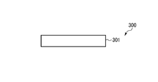
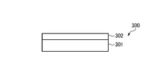
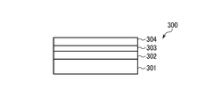
- FIGS. 2A to 2C Specific examples of the substrate are shown in FIGS. 2A to 2C.
- a semiconductor wafer can be typically mentioned as the substrate 300.
- Examples of the substrate 300 include those shown in FIGS. 2A, 2B, and 2C.
- the substrate 300 is composed only of the semiconductor substrate 301 formed of a semiconductor such as silicon.
- an insulating film 302 such as a SiO 2 film is formed on a semiconductor substrate 301 such as silicon.
- the substrate 300 is a metal such as a Cu film via an insulating film 302 such as a SiO 2 film and a barrier film 303 such as a TaN film, a Ta film, or a TiN film on a semiconductor substrate 301 such as silicon.
- the film 304 is formed.
- the barrier film 303 may be omitted.
- the barrier film 303 may be a laminated film (for example, Ta / TaN).
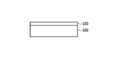
- step 2 the substrate 300 is housed in the processing container, the substrate 300 is heated to a predetermined temperature, and the first processing gas containing the carbon-containing gas is supplied to the substrate 300. As a result, as shown in FIG. 3, a core 310 for forming a graphene structure is formed on the surface of the substrate 300.
- the first process gas used in the step 2 may be only a carbon-containing gas, it may be contained in addition to the hydrogen gas of the carbon-containing gas (H 2 gas). It may also contain a diluting gas or a rare gas as a carrier gas. As the rare gas, Ar, He, Ne, Kr, Xe and the like can be used.
- a highly reactive gas is preferable, and a hydrocarbon gas is preferable.
- hydrocarbon gases those having an unsaturated bond and those having a small number of carbon atoms are more reactive and preferable.
- acetylene (C 2 H 2 ) having a triple bond with 2 carbon atoms ethylene (C 2 H 4 ) having a double bond, and propylene (C 3 H 6 ) having a double bond with 3 carbon atoms. It can be preferably used.
- Hydrocarbons that do not have unsaturated bonds such as methane (CH 4 ), ethane (C 2 H 6 ), and propane (C 3 H 8 ), may be used.
- H 2 gas can be added to control nucleation.
- the formation of graphene proceeds with nucleation and creeping growth based on the following chemical equilibrium equation.
- C x H y ⁇ C (graphene) + H 2 Therefore, the nucleation of graphene can be controlled by adding H 2 gas.
- the temperature of the substrate when carrying out step 2 is preferably 300 to 1000 ° C. More preferably, it is 350 to 750 ° C.
- the pressure in the processing container is preferably in the range of 1.33 to 1330 Pa (0.01 to 10 Torr), more preferably 1.33 to 133 Pa (0.01 to 1 Torr).
- the processing time is preferably 30 sec or more, more preferably 1 to 10 min.
- step 2 By performing the pretreatment in step 2 in this way, nuclei for forming the graphene structure are formed, and the nucleation density is controlled. This makes it possible to improve the coverage of the graphene structure by the plasma CVD of step 3 which is subsequently performed.
- the graphene structure is formed on the substrate 300 as shown in FIG. 4 by causing the plasma of the second processing gas containing the carbon-containing gas to act on the substrate 300 on which the nucleus 310 is formed. Grow 320.
- the plasma at this time is not particularly limited, but it is preferable to use microwave plasma, particularly remote microwave plasma.
- the remote microwave plasma means that a microwave is introduced into a processing container to generate plasma by a microwave electric field, and the plasma is diffused from the plasma generation region to a substrate 300 arranged at a position away from the plasma generation region. A plasma that acts on a plasma.
- the carbon-containing gas can be dissociated into a state suitable for the growth of the graphene structure at a relatively low temperature.
- a rare gas may be used as the second processing gas in addition to the carbon-containing gas used as the film forming raw material.
- the rare gas can be used as a plasma generating gas. That is, microwaves are introduced into the processing container and a plasma generating gas composed of a rare gas is introduced to generate microwave plasma. Then, the carbon-containing gas, which is the film-forming raw material gas, is dissociated by plasma and supplied to the substrate 300 away from the plasma generation region, and the graphene structure 320 is grown on the substrate 300.
- Ar As the rare gas contained in the second processing gas, Ar, He, Ne, Kr, Xe and the like can be used, but among these, Ar capable of stably generating plasma is preferable.
- Examples of the carbon-containing gas contained in the second treatment gas include ethylene (C 2 H 4 ), methane (CH 4 ), ethane (C 2 H 6 ), propane (C 3 H 8 ), and propylene (C 3 H). 6 ) Hydrocarbon gas such as acetylene (C 2 H 2 ) and alcohol gas such as methanol (CH 3 OH) and ethanol (C 2 H 5 OH) can be used.
- the carbon-containing gas used here may be the same as or different from the carbon-containing gas used in step 2.
- the second processing gas may also contain a hydrogen-containing gas, for example, H 2 gas.
- the hydrogen-containing gas can improve the quality of the graphene structure.
- an oxidizing gas such as oxygen gas (O 2 gas) and water vapor (H 2 O gas) may be contained. Defects contained in the graphene structure can be etched with an oxidizing gas to enhance crystallinity.
- the film-forming raw material gas can be introduced at an arbitrary position between the plasma generation region and the region near the substrate, depending on the required degree of dissociation. That is, in the plasma generation region, the degree of dissociation is increased by high-energy plasma, and in the region near the substrate, the degree of dissociation is lower than that in the plasma generation region due to the low electron temperature plasma diffused from the plasma generation region. Therefore, the degree of dissociation of the film-forming raw material gas can be adjusted by the introduction position of the film-forming raw material gas.
- the substrate is arranged in a region away from the microwave plasma generation region, and plasma diffused from the plasma generation region is supplied to the substrate. Therefore, the plasma has a low electron temperature on the substrate, has low damage, and becomes a high-density plasma mainly composed of radicals by microwaves.
- the graphene structure may be only ordinary graphene formed parallel to the substrate, or may contain carbon nanowalls (CNW) grown at an angle with respect to the substrate in addition to graphene.
- CCW carbon nanowalls
- the process conditions are preferably such that the substrate temperature is 350 to 1000 ° C. (more preferably 400 to 800 ° C.) and the microwave power is 100 to 5000 W.
- the pressure in the processing container is 1.33 to 667 Pa (0.01 to 5 Torr) when the surface of the substrate is an insulator and a semiconductor, and 1.33 to 400 Pa (0) when the surface of the substrate is metal. It is preferably 0.01 to 3 Torr).
- the time is preferably in the range of 1 to 200 min.
- the graphene core prior to film formation of the graphene structure by plasma CVD, the graphene core is supplied to the substrate by supplying a gas containing a carbon-containing gas to the substrate while heating the substrate without using plasma. It is possible to form. Therefore, in the subsequent plasma CVD, nucleation and creeping growth are promoted, and a graphene structure having high coverage can be formed. Therefore, it is not necessary to use the activated metal catalyst layer.
- a surface treatment for the purpose of cleaning the surface of the substrate may be performed prior to the pretreatment step of step 2.
- the surface treatment include a treatment of supplying H 2 gas or Ar gas + H 2 gas while heating the substrate to 300 to 600 ° C. At this time, plasma may be generated.
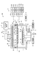
- FIG. 5 is a cross-sectional view schematically showing a first example of the processing apparatus.
- the processing apparatus 100 shown in FIG. 5 is configured as, for example, an RLSA (registered trademark) microwave plasma type plasma processing apparatus.
- the processing device 100 includes a processing container 1, a mounting table 2, a microwave introduction mechanism 3, a gas supply mechanism 4, an exhaust unit 5, and a control unit 6.
- the processing container 1 has a substantially cylindrical shape.
- a circular opening 10 is formed in the substantially central portion of the bottom wall 1a of the processing container 1, and the bottom wall 1a is provided with an exhaust chamber 11 that communicates with the opening 10 and projects downward.
- an exhaust chamber 11 that communicates with the opening 10 and projects downward.
- a carry-in outlet 17 for loading and unloading the wafer W and a gate valve 18 for opening and closing the carry-in outlet 17 are provided on the side wall of the processing container 1.
- the mounting table 2 is provided in the processing container 1 and mounts, for example, a semiconductor wafer (hereinafter, simply referred to as a wafer) W as a substrate.
- the mounting table 2 has a disk shape and is made of ceramics such as AlN, and is supported by a support member 12 made of ceramics such as cylindrical AlN extending upward from the center of the bottom of the exhaust chamber 11.
- a guide ring 13 for guiding the wafer W is provided on the outer edge of the mounting table 2.
- a lifting pin (not shown) for raising and lowering the wafer W is provided so as to be retractable with respect to the upper surface of the mounting table 2.
- a resistance heating type heater 14 is embedded inside the mounting table 2.
- the heater 14 is supplied with power from the heater power supply 15 to heat the wafer W on the mounting table 2 via the mounting table 2. Further, a thermocouple (not shown) is inserted in the mounting table 2, and the heating temperature of the wafer W is controlled to a predetermined temperature in the range of, for example, 300 to 1000 ° C. based on the signal from the thermocouple. It is possible. Further, an electrode 16 having the same size as the wafer W is embedded above the heater 14 in the mounting table 2, and a high frequency bias power supply 19 is electrically connected to the electrode 16. A high frequency bias for drawing ions is applied from the high frequency bias power supply 19 to the mounting table 2. The high frequency bias power supply 19 may not be provided depending on the characteristics of plasma processing.
- the microwave introduction mechanism 3 is for introducing microwaves into the processing container 1, and is provided so as to face the opening at the upper part of the processing container 1.
- the microwave introduction mechanism 3 includes a flat slot antenna 21, a microwave generation unit 22, and a microwave transmission mechanism 23.
- the flat slot antenna 21 is made of, for example, a silver or gold-plated copper plate or aluminum plate on the surface, and is formed so that a plurality of slots 21a for radiating microwaves penetrate in a predetermined pattern.
- the pattern of slot 21a is appropriately set so that microwaves are evenly emitted.
- An example of a suitable pattern is a radial line slot in which two pairs of slots 21a arranged in a T shape are paired and a plurality of pairs of slots 21a are arranged concentrically.
- the length and arrangement spacing of the slots 21a are appropriately determined according to the effective wavelength ( ⁇ g) of the microwave.
- the slot 21a may have another shape such as a circular shape or an arc shape.
- the arrangement form of the slots 21a is not particularly limited, and the slots 21a can be arranged concentrically, for example, spirally or radially.
- the pattern of the slot 21a is appropriately set so as to have microwave radiation characteristics that can obtain a desired plasma density distribution.
- a microwave transmission plate 24 made of a dielectric material is provided so as to be supported by an upper plate 32 provided in a ring shape on the upper part of the processing container 1. Further, a shield member 25 having a water-cooled structure is provided on the flat slot antenna 21. Further, a slow wave material 26 is provided between the shield member 25 and the flat slot antenna 21.
- the slow wave material 26 is made of a dielectric having a dielectric constant larger than that of vacuum, for example, a resin such as quartz, ceramics (Al 2 O 3 ), polytetrafluoroethylene, or polyimide.
- the slow wave material 26 has a function of making the wavelength of the microwave shorter than that in vacuum to make the flat slot antenna 21 smaller.
- the microwave transmission plate 24 is also made of the same dielectric material.
- the thickness of the microwave transmission plate 24 and the slow wave material 26 is adjusted so that the slow wave material 26, the flat slot antenna 21, the microwave transmission plate 24, and the equivalent circuit formed by the plasma satisfy the resonance condition.
- the thickness of the slow wave material 26 the phase of the microwave can be adjusted.
- the thickness so that the junction of the flat slot antenna 21 becomes a "hara" of a standing wave the reflection of the microwave is minimized and the radiant energy of the microwave is maximized. Further, by using the same material for the slow wave material 26 and the microwave transmission plate 24, interfacial reflection of microwaves can be prevented.
- the microwave generation unit 22 is for generating microwaves and has a microwave oscillator.
- the microwave oscillator may be a magnetron or a solid state.
- the frequency of the microwave oscillated from the microwave oscillator can be in the range of 300 MHz to 10 GHz.
- a magnetron as a microwave oscillator, it is possible to oscillate a microwave having a frequency of 2.45 GHz.
- the microwave transmission mechanism 23 is for guiding the microwave from the microwave generating unit 22 to the planar slot antenna 21.
- the microwave transmission mechanism 23 includes a waveguide 27, a coaxial waveguide 28, and a mode conversion mechanism 31.
- the waveguide 27 guides microwaves from the microwave generation unit 22 and extends in the horizontal direction.
- the coaxial waveguide 28 includes an inner conductor 29 extending upward from the center of the planar slot antenna 21 and an outer conductor 30 outside the inner conductor 29.
- the mode conversion mechanism 31 is provided between the waveguide 27 and the coaxial waveguide 28, and is for converting the vibration mode of the microwave.
- the microwave generated by the microwave generating unit 22 propagates in the waveguide 27 in the TE mode, the vibration mode of the microwave is converted from the TE mode to the TEM mode by the mode conversion mechanism 31, and the microwave is transmitted through the coaxial waveguide 28. Is guided to the slow waveguide 26. Then, the microwave is radiated from the slow wave material 26 into the processing container 1 via the slot 21a of the flat slot antenna 21 and the microwave transmission plate 24.
- a tuner (not shown) is provided in the middle of the waveguide 27 to match the impedance of the load (plasma) in the processing container 1 with the characteristic impedance of the power supply of the microwave generating unit 22.
- the gas supply mechanism 4 has a shower plate 41 horizontally provided above the mounting table in the processing container 1 so as to partition the top and bottom, and a ring shape along the inner wall of the processing container 1 at the position above the shower plate 41. It has a shower ring 42 provided in.
- the shower plate 41 includes a gas flow member 51 formed in a grid pattern, a gas flow path 52 provided in a grid pattern inside the gas flow path member 51, and a large number of gases extending downward from the gas flow path 52. It has a discharge hole 53.
- the portion between the lattice-shaped gas passage members 51 is a through hole 54.
- a gas supply path 55 reaching the outer wall of the processing container 1 extends to the gas flow path 52 of the shower plate 41, and a gas supply pipe 56 is connected to the gas supply path 55.
- the gas supply pipe 56 is branched into four branch pipes 56a, 56b, 56c, and 56d.
- the branch pipe 56a, the H 2 gas to supply H 2 gas supply source 57 is connected to a hydrogen-containing gas.
- a C 2 H 2 gas supply source 58a for supplying acetylene (C 2 H 2 ) gas as a carbon-containing gas used for the first processing gas is connected to the branch pipe 56b.
- a C 2 H 4 gas supply source 58 b for supplying ethylene (C 2 H 4 ) gas as a carbon-containing gas used for the second processing gas is connected to the branch pipe 56c.
- the branch pipe 56d, the N 2 gas supply source 59 for supplying N 2 gas used as a purge gas or the like is connected.
- the branch pipes 56a, 56b, 56c, and 56d are provided with a mass flow controller for flow rate control and valves before and after the mass flow controller.
- the shower ring 42 has a ring-shaped gas flow path 66 provided inside the shower ring 42, and a large number of gas discharge holes 67 connected to the gas flow path 66 and opened inside the gas flow path 66. Is connected to the gas supply pipe 61.
- the gas supply pipe 61 is branched into three branch pipes 61a, 61b, and 61c.
- An Ar gas supply source 62 for supplying Ar gas as a rare gas which is a plasma generating gas is connected to the branch pipe 61a.
- An O 2 gas supply source 63 for supplying an O 2 gas which is an oxidizing gas for etching a defect (non-graphene structure) is connected to the branch pipe 61b.
- the branch pipe 61c, N 2 gas supply source 64 for supplying N 2 gas used as a purge gas or the like is connected.
- the branch pipes 61a, 61b, and 61c are provided with a mass flow controller for flow rate control and valves before and after the mass flow controller.
- the carbon-containing gas, oxidizing gas, and rare gas are not limited to those described, and the above-mentioned various gases can be used.
- the exhaust unit 5 is for exhausting the inside of the processing container 1, the exhaust chamber 11, the exhaust pipe 81 provided on the side surface of the exhaust chamber 11, the vacuum pump connected to the exhaust pipe 81, and the pressure control. It has an exhaust device 82 having a valve or the like.
- the control unit 6 typically consists of a computer and controls each unit of the processing device 100.
- the control unit 6 includes a storage unit that stores the process sequence of the processing device 100 and the process recipe that is a control parameter, an input means, a display, and the like, and can perform predetermined control according to the selected process recipe. ..
- the wafer W is carried into the processing container 1 as a substrate and placed on the mounting table 2. If necessary, the surface of the wafer W is cleaned.
- the pressure in the processing container 1 and the wafer temperature are controlled to predetermined values, and the first processing gas containing the carbon-containing gas is supplied to the substrate to perform the pretreatment in step 2.
- the first processing gas Ar gas, which is a rare gas, is supplied from the shower ring 42, and C 2 H 2 gas as a carbon-containing gas is supplied from the shower plate 41. At this time, H 2 gas may be supplied as needed.
- the pretreatment of step 2 forms the core of the graphene structure on the surface of the substrate.
- the pressure in the processing container 1 and the wafer temperature are controlled to predetermined values, and the graphene structure is formed by the remote microwave plasma CVD in step 3.
- Ar gas which is a plasma generating gas
- Ar gas is supplied from the shower ring 42 directly under the microwave transmission plate 24, and the microwave generated by the microwave generating unit 22 is radiated into the processing container 1 to generate plasma. Ignite.
- the microwave generated by the microwave generation unit 22 is guided to the slow wave material 26 via the waveguide 27, the mode conversion mechanism 31, and the coaxial waveguide 28, and is guided from the slow wave material 26 to the slot 21a of the flat slot antenna 21. And it is radiated into the processing container 1 through the microwave transmission plate 24.
- the microwave spreads as a surface wave to the region directly below the microwave transmission plate 24, and surface wave plasma by Ar gas is generated, and that region becomes a plasma generation region.
- C 2 H 4 gas as a carbon-containing gas which is a film-forming raw material gas, is supplied from the shower plate 41.
- H 2 gas and O 2 gas may be supplied as needed.
- These gases are excited and dissociated by the plasma diffused from the plasma generation region, and are supplied to the wafer W, which is a substrate mounted on the mounting table 2 below the shower plate 41.
- the wafer W is arranged in a region away from the plasma generation region, and since the plasma diffused from the plasma generation region is supplied to the wafer W, the plasma becomes low electron temperature plasma on the wafer W and the damage is low. Moreover, it becomes a high-density plasma mainly composed of radicals.
- a graphene structure can be formed on the surface of the substrate on which the nuclei are formed according to a general crystal growth mode of nucleation and creeping growth.
- the C 2 H 4 gas as the carbon-containing gas and, if necessary, the H 2 gas are supplied from the shower plate 41 below the plasma generation region and dissociated by the diffused plasma, so that these gases are excessive. Dissociation can be suppressed.
- these gases may be supplied to the plasma generation region.
- Ar gas which is a plasma generation gas and C 2 H 4 gas which is a carbon-containing gas or the like may be supplied to the plasma generation region to directly ignite the plasma.
- Preferred conditions for remote microwave plasma CVD in the processing apparatus 100 are as follows.
- the wafer surface is an insulator and
- the carbon-containing gas in the first treatment gas and the carbon-containing gas in the second treatment gas may be the same gas, and for example, both C 2 H 2 gas can be used. In that case, the C 2 H 4 gas supply source 58b is unnecessary.
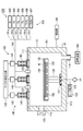
- FIG. 6 is a cross-sectional view schematically showing a second example of the processing apparatus
- FIG. 7 is a configuration diagram showing a configuration of a microwave introducing apparatus of the processing apparatus of FIG. 6, and
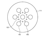
- FIG. 9 is a bottom view schematically showing the top wall portion of the processing container in the processing apparatus of FIG.
- the processing device 200 includes a processing container 101, a mounting table 102, a gas supply mechanism 103, an exhaust device 104, a microwave introduction device 105, and a control unit 106.
- the processing container 101 accommodates the wafer W, is formed of a metal material such as aluminum and an alloy thereof, has a substantially cylindrical shape, and has a plate-shaped top wall portion 111 and a bottom wall portion 113, and these. It has a side wall portion 112 that connects the two.
- the microwave introduction device 105 is provided above the processing container 101 and functions as a plasma generation means for introducing an electromagnetic wave (microwave) into the processing container 101 to generate plasma.
- the microwave introduction device 105 will be described in detail later.
- the top wall portion 111 has a plurality of openings into which the microwave radiation mechanism and the gas introduction portion described later of the microwave introduction device 105 are fitted.
- the side wall portion 112 has a carry-in / out port 114 for carrying in / out the wafer W, which is a substrate, to and from a transport chamber (not shown) adjacent to the processing container 101.
- the carry-in outlet 114 is opened and closed by a gate valve 115.
- An exhaust device 104 is provided on the bottom wall portion 113.
- the exhaust device 104 is provided in an exhaust pipe 116 connected to the bottom wall portion 113, and includes a vacuum pump and a pressure control valve.
- the inside of the processing container 101 is exhausted through the exhaust pipe 116 by the vacuum pump of the exhaust device 104.
- the pressure in the processing container 101 is controlled by the pressure control valve.
- the mounting table 102 is arranged inside the processing container 101 and mounts the wafer W.
- the mounting table 102 has a disk shape and is made of ceramics such as AlN.
- the mounting table 102 is supported by a support member 120 made of ceramics such as cylindrical AlN extending upward from the center of the bottom of the processing container 101.
- a guide ring 181 for guiding the wafer W is provided on the outer edge of the mounting table 102.
- an elevating pin (not shown) for raising and lowering the wafer W is provided so as to be retractable with respect to the upper surface of the mounting table 102.
- a resistance heating type heater 182 is embedded inside the mounting table 102, and the heater 182 heats the wafer W on the mounting table 102 by supplying power from the heater power supply 183.
- a thermocouple (not shown) is inserted in the mounting table 102, and the heating temperature of the wafer W is controlled to a predetermined temperature in the range of, for example, 350 to 1000 ° C. based on the signal from the thermocouple. It is possible.
- an electrode 184 having the same size as the wafer W is embedded above the heater 182 in the mounting table 102, and a high frequency bias power supply 122 is electrically connected to the electrode 184. A high-frequency bias for drawing ions is applied from the high-frequency bias power supply 122 to the mounting table 102.
- the high frequency bias power supply 122 may not be provided depending on the characteristics of plasma processing.
- the gas supply mechanism 103 is for introducing the plasma generation gas and the raw material gas for forming the graphene structure into the processing container 101, and has a plurality of gas introduction nozzles 123.
- the gas introduction nozzle 123 is fitted into an opening formed in the top wall portion 111 of the processing container 101.
- a gas supply pipe 191 is connected to the gas introduction nozzle 123.
- the gas supply pipe 191 is branched into six branch pipes 191a, 191b, 191c, 191d, 191e, and 191f.
- An Ar gas supply source 192 for supplying Ar gas as a rare gas which is a plasma generating gas is connected to the branch pipe 191a.
- the branch pipe 191c, the N 2 gas supply source 194 for supplying a N 2 gas used as a purge gas or the like is connected.
- the branch pipe 191d, the H 2 gas to supply H 2 gas supply source 195 is connected to a hydrogen-containing gas.
- a C 2 H 2 gas supply source 196 for supplying acetylene (C 2 H 2 ) gas as a carbon-containing gas used for the first processing gas is connected to the branch pipe 191e.
- a C 2 H 4 gas supply source 197 that supplies ethylene (C 2 H 4 ) gas as a carbon-containing gas used for the second processing gas is connected to the branch pipe 191 f.
- the branch pipes 191a, 191b, 191c, 191d, 191e, and 191f are provided with a mass flow controller for flow rate control and valves before and after the mass flow controller.
- the shower plate provided C 2 H 4 gas or the like so as to be supplied to a position close to the wafer W to adjust the dissociation of the gas. Further, the same effect can be obtained by extending the nozzle for supplying these gases downward.
- the carbon-containing gas, the oxidizing gas, and the rare gas are not limited to those described, and various gases described above can be used.
- the microwave introduction device 105 is provided above the processing container 101 and functions as a plasma generation means for introducing electromagnetic waves (microwaves) into the processing container 101 to generate plasma.
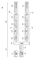
- the microwave introduction device 105 includes a top wall portion 111 of the processing container 101 that functions as a top plate, a microwave output portion 130, and an antenna unit 140.
- the microwave output unit 130 generates microwaves and distributes and outputs microwaves to a plurality of paths.
- the microwave output unit 130 includes a microwave power supply 131, a microwave oscillator 132, an amplifier 133, and a distributor 134.
- the microwave oscillator 132 is in a solid state and oscillates microwaves (for example, PLL oscillation) at 860 MHz, for example.
- the microwave frequency is not limited to 860 MHz, and those in the range of 700 MHz to 10 GHz such as 2.45 GHz, 8.35 GHz, 5.8 GHz, 1.98 GHz and the like can be used.
- the amplifier 133 amplifies the microwave oscillated by the microwave oscillator 132.
- the distributor 134 distributes the microwave amplified by the amplifier 133 to a plurality of paths, and distributes the microwave while matching the impedances on the input side and the output side.
- the antenna unit 140 introduces the microwave output from the microwave output unit 130 into the processing container 101.
- the antenna unit 140 includes a plurality of antenna modules 141.
- Each of the plurality of antenna modules 141 introduces microwaves distributed by the distributor 134 into the processing container 101.
- the configurations of the plurality of antenna modules 141 are all the same.
- Each antenna module 141 has an amplifier unit 142 that mainly amplifies and outputs the distributed microwaves, and a microwave radiation mechanism 143 that radiates the microwaves output from the amplifier unit 142 into the processing container 101.
- the amplifier unit 142 includes a phase device 145, a variable gain amplifier 146, a main amplifier 147, and an isolator 148.
- the phase device 145 changes the phase of the microwave.
- the variable gain amplifier 146 adjusts the power level of the microwave input to the main amplifier 147.
- the main amplifier 147 is configured as a solid state amplifier.
- the isolator 148 separates the reflected microwaves reflected by the antenna portion of the microwave radiation mechanism 143, which will be described later, toward the main amplifier 147.
- the microwave radiation mechanism 143 includes a coaxial tube 151, a feeding unit 155, a tuner 154, and an antenna unit 156.
- the coaxial tube 151 has an outer conductor 152 forming a tubular shape and an inner conductor 153 provided coaxially with the outer conductor 152 in the outer conductor 152, and has a microwave transmission line between them.
- the power feeding unit 155 feeds the amplified microwave from the amplifier unit 142 to the microwave transmission line.
- Microwaves amplified by the amplifier section 142 by the coaxial cable are introduced into the feeding section 155 from the side of the upper end portion of the outer conductor 152.
- microwave power is supplied to the microwave transmission line between the outer conductor 152 and the inner conductor 153, and the microwave power propagates toward the antenna portion 156.
- the antenna portion 156 radiates microwaves from the coaxial tube 151 into the processing container 101, and is provided at the lower end portion of the coaxial tube 151.
- the antenna portion 156 is arranged on a disk-shaped flat antenna 161 connected to the lower end of the inner conductor 153, a slow wave material 162 arranged on the upper surface side of the flat antenna 161 and a lower surface side of the flat antenna 161. It also has a microwave transmission plate 163.
- the microwave transmission plate 163 is fitted in the top wall portion 111, and the lower surface thereof is exposed in the internal space of the processing container 101.
- the planar antenna 161 has a slot 161a formed so as to penetrate the flat antenna 161. The shape of slot 161a is appropriately set so that microwaves are efficiently radiated.
- a dielectric may be inserted in the slot 161a.
- the slow wave material 162 is made of a material having a dielectric constant larger than that of vacuum, and the phase of the microwave can be adjusted by the thickness thereof so that the radiant energy of the microwave is maximized. it can.
- the microwave transmission plate 163 is also made of a dielectric and has a shape capable of efficiently radiating microwaves in the TE mode. Then, the microwave transmitted through the microwave transmission plate 163 generates plasma in the space inside the processing container 101.
- the material constituting the slow wave material 162 and the microwave transmission plate 163 for example, quartz, ceramics, a fluorine-based resin such as polytetrafluoroethylene resin, a polyimide resin, or the like can be used.
- the tuner 154 matches the impedance of the load with the characteristic impedance of the microwave power supply 131.
- the tuner 154 constitutes a slug tuner.
- the tuner 154 has two slugs 171a and 171b, an actuator 172 that independently drives these two slugs, and a tuner controller 173 that controls the actuator 172. ..
- the slags 171a and 171b are arranged on the base end side (upper end side) of the coaxial tube 151 with respect to the antenna portion 156.
- the slags 171a and 171b are plate-shaped and annular, are made of a dielectric material such as ceramics, and are arranged between the outer conductor 152 and the inner conductor 153 of the coaxial tube 151. Further, the actuator 172 individually drives the slags 171a and 171b by rotating two screws provided inside the inner conductor 153, respectively, in which the slags 171a and 171b are screwed. Then, based on the command from the tuner controller 173, the actuator 172 moves the slags 171a and 171b in the vertical direction. The tuner controller 173 adjusts the positions of the slags 171a and 171b so that the impedance at the end portion becomes 50 ⁇ .
- the main amplifier 147, the tuner 154, and the planar antenna 161 are arranged close to each other.
- the tuner 154 and the planar antenna 161 form a lumped constant circuit and function as a resonator. Although there is an impedance mismatch in the mounting portion of the flat antenna 161, it is tuned directly to the plasma load by the tuner 154, so that it can be tuned with high accuracy including the plasma. Therefore, the influence of reflection on the flat antenna 161 can be eliminated.
- the corresponding microwave transmission plates 163 are arranged evenly in a hexagonal close-packed arrangement. That is, one of the seven microwave transmission plates 163 is arranged in the center of the top wall portion 111, and the other six microwave transmission plates 163 are arranged around the center. These seven microwave transmission plates 163 are arranged so that adjacent microwave transmission plates are evenly spaced. Further, the plurality of nozzles 123 of the gas supply mechanism 103 are arranged so as to surround the periphery of the central microwave transmission plate.
- the arrangement of the microwave radiation mechanism 143 is not limited to this, and the number thereof is not limited to seven.
- the control unit 106 is typically composed of a computer and controls each unit of the processing device 200.
- the control unit 106 includes a storage unit that stores the process sequence of the processing device 200 and the process recipe that is a control parameter, an input means, a display, and the like, and can perform predetermined control according to the selected process recipe. ..
- a wafer W whose surface is made of an insulator, a semiconductor, or a metal as a substrate is carried into the processing container 101. It is placed on the mounting table 102. If necessary, the surface of the wafer W is cleaned.
- the pressure in the processing container 101 and the wafer temperature are controlled to predetermined values, and the first processing gas containing the carbon-containing gas is supplied to the substrate to perform the pretreatment in step 2.
- the first processing gas Ar gas, which is a rare gas, and C 2 H 2 gas as a carbon-containing gas are supplied from the gas introduction nozzle 123. At this time, H 2 gas may be supplied as needed.
- Step 2 forms the core of the graphene structure on the surface of the substrate.
- the pressure in the processing container 101 and the wafer temperature are controlled to predetermined values, and the graphene structure is formed by the remote microwave plasma CVD in step 3.
- Ar gas which is a plasma generating gas
- Ar gas is supplied from the gas introduction nozzle 123 directly below the top wall portion 111 of the processing container 101, and microwaves are radiated into the processing container 101 to ignite the plasma.
- the radiated microwaves are distributed to a plurality of microwaves from the microwave output unit 130 of the microwave introduction device 105 and output, and the microwaves are guided to a plurality of antenna modules 141 of the antenna unit 140 to guide these microwave radiation mechanisms. It was emitted from 143.
- each antenna module 141 microwaves are individually amplified by the main amplifier 147 constituting the solid state amplifier, fed to each microwave radiation mechanism 143, transmitted through the coaxial tube 151, and reach the antenna unit 156.
- the impedance of the microwave is automatically matched by the slugs 171a and 171b of the tuner 154. Therefore, the microwave is radiated from the tuner 154 through the slow wave material 162 of the antenna portion 156 and from the slot 161a of the flat antenna 161 in a state where there is substantially no power reflection.
- the microwave further passes through the microwave transmission plate 163 and is transmitted on the surface (lower surface) of the microwave transmission plate 163 in contact with the plasma to form a surface wave.
- the electric power from each antenna portion 156 is spatially combined in the processing container 101, a surface wave plasma by Ar gas is generated in a region directly below the top wall portion 111, and that region becomes a plasma generation region.
- C 2 H 4 gas as a carbon-containing gas which is a film-forming raw material gas, is supplied from the gas introduction nozzle 123.
- H 2 gas and O 2 gas may be supplied as needed.
- the wafer W which is a substrate mounted on the mounting table 102.
- the wafer W is arranged in a region away from the plasma generation region, and since the plasma diffused from the plasma generation region is supplied to the wafer W, the plasma becomes low electron temperature plasma on the wafer W and the damage is low. Moreover, it becomes a high-density plasma mainly composed of radicals. With such plasma, a graphene structure can be formed according to a general crystal growth mode of nucleation and creeping growth.
- the C 2 H 4 gas as the carbon-containing gas and, if necessary, the H 2 gas are supplied to the plasma generation region and dissociated.
- C 2 H 4 gas and, if necessary, H 2 gas are dissociated by the plasma diffused from the plasma generation region. May be suppressed.
- Ar gas which is a plasma generation gas and C 2 H 4 gas which is a carbon-containing gas or the like may be supplied to the plasma generation region to directly ignite the plasma.
- the microwaves distributed in a plurality of regions are individually amplified by the main amplifier 147 constituting the solid state amplifier, and individually introduced into the processing container 101 from the plurality of antenna units 156 to form a surface wave. After forming, these are combined in space to generate microwave plasma. This eliminates the need for large isolators and synthesizers and is compact. Further, the main amplifier 147, the tuner 154 and the planar antenna 161 are provided in close proximity to each other, and the tuner 154 and the planar antenna 161 form a lumped constant circuit and function as a resonator.
- the tuner 154 can tune the flat slot antenna mounting portion where impedance mismatch exists with high precision including plasma, so that the influence of reflection can be reliably eliminated and high-precision plasma control becomes possible. .. Further, since the plurality of microwave transmission plates 163 are provided, the total area can be reduced as compared with the single microwave transmission plate 24 in the processing apparatus of the first example. Therefore, the microwave power required to stably ignite and discharge the plasma can be reduced.
- the preferable conditions for remote microwave plasma CVD in the processing apparatus 200 are basically the same as those in the first example, but the more preferable conditions differ depending on the item, and are as follows.
- the carbon-containing gas in the first processing gas and the carbon-containing gas in the second processing gas may be the same gas, for example, both of them use C 2 H 2 gas. Can be used. In that case, the C 2 H 4 gas supply source 197 is unnecessary.
- Example 1 a bare Si substrate was prepared as the substrate, and the effect of the pretreatment performed prior to the film formation of the graphene structure by plasma CVD was confirmed.
- the first treatment gas C 2 H 2 gas, H 2 gas, and Ar gas were used, and the flow rates were set to 1 sccm, 0.1 sccm, and 50 sccm, respectively.
- the pressure was 0.4 Torr
- the substrate temperature was 700 ° C.
- the treatment time was changed to 0 sec (no treatment), 180 sec, and 600 sec.
- FIG. 10 is an AFM photograph showing these surface states. As shown in FIG. 10, when the treatment was not performed (0 sec), the surface roughness RMS was 0.095 nm, whereas when the treatment times were 180 sec and 600 sec, the RMS was 0.098 nm and 0.103 nm, respectively. The value of RMS has increased.
- FIG. 11 shows the relationship between the processing time and the RMS value at this time, and as shown in this figure, it can be seen that the RMS value increases as the processing time becomes longer.
- FIG. 12 shows the Raman spectrum of the substrate surface when the processing time is 0 sec, 180 sec, and 600 sec. From FIG. 12, it can be seen that the background intensity of the Raman spectrum increases as the processing time becomes longer. ..
- microcrystals or carbon without a clear structure may be present on the substrate surface by treating with a processing gas containing a carbon-containing gas prior to plasma CVD. ..
- Example 2 a graphene structure was formed by plasma CVD after surface treatment and pretreatment were performed on the Si substrate, which is a substrate, using the processing apparatus of the first example shown in FIG.
- the surface treatment and plasma CVD were carried out under fixed conditions, and the time during the pretreatment was changed.
- FIG. 14 is a diagram showing the relationship between the pretreatment time and the D band intensity (arbitrary unit). As shown in this figure, it was confirmed that the D-band strength, that is, the amount of film formed increased with the increase in the pretreatment time. Further, FIG. 15 shows SEM photographs of the surface when the pretreatment time is 10 sec, 60 sec, and 120 sec, and it can be seen from the SEM photographs that the coverage increases as the pretreatment time increases.
- plasma CVD is not limited to microwave plasma CVD.
- processing device for performing remote microwave plasma CVD is not limited to the above example, and various types of processing devices can be used.
- a substrate for forming a graphene structure a semiconductor wafer based on a semiconductor such as Si has been described as an example, but the present invention is not limited to this.
Landscapes
- Chemical & Material Sciences (AREA)
- Engineering & Computer Science (AREA)
- Physics & Mathematics (AREA)
- Plasma & Fusion (AREA)
- Organic Chemistry (AREA)
- Chemical Kinetics & Catalysis (AREA)
- Computer Hardware Design (AREA)
- Microelectronics & Electronic Packaging (AREA)
- Power Engineering (AREA)
- Condensed Matter Physics & Semiconductors (AREA)
- Manufacturing & Machinery (AREA)
- General Physics & Mathematics (AREA)
- General Chemical & Material Sciences (AREA)
- Materials Engineering (AREA)
- Mechanical Engineering (AREA)
- Metallurgy (AREA)
- Analytical Chemistry (AREA)
- Inorganic Chemistry (AREA)
- Nanotechnology (AREA)
- Electromagnetism (AREA)
- Spectroscopy & Molecular Physics (AREA)
- Carbon And Carbon Compounds (AREA)
- Plasma Technology (AREA)
- Chemical Vapour Deposition (AREA)
Priority Applications (2)
| Application Number | Priority Date | Filing Date | Title |
|---|---|---|---|
| US17/593,220 US12014907B2 (en) | 2019-03-15 | 2020-02-26 | Method and device for forming graphene structure |
| KR1020217032269A KR102650973B1 (ko) | 2019-03-15 | 2020-02-26 | 그래핀 구조체를 형성하는 방법 및 장치 |
Applications Claiming Priority (2)
| Application Number | Priority Date | Filing Date | Title |
|---|---|---|---|
| JP2019-049093 | 2019-03-15 | ||
| JP2019049093A JP7178935B2 (ja) | 2019-03-15 | 2019-03-15 | グラフェン構造体を形成する方法および装置 |
Publications (1)
| Publication Number | Publication Date |
|---|---|
| WO2020189202A1 true WO2020189202A1 (ja) | 2020-09-24 |
Family
ID=72430399
Family Applications (1)
| Application Number | Title | Priority Date | Filing Date |
|---|---|---|---|
| PCT/JP2020/007748 Ceased WO2020189202A1 (ja) | 2019-03-15 | 2020-02-26 | グラフェン構造体を形成する方法および装置 |
Country Status (4)
| Country | Link |
|---|---|
| US (1) | US12014907B2 (enExample) |
| JP (1) | JP7178935B2 (enExample) |
| KR (1) | KR102650973B1 (enExample) |
| WO (1) | WO2020189202A1 (enExample) |
Families Citing this family (4)
| Publication number | Priority date | Publication date | Assignee | Title |
|---|---|---|---|---|
| JP2022079159A (ja) * | 2020-11-16 | 2022-05-26 | 東京エレクトロン株式会社 | 基板処理方法および基板処理装置 |
| US11515163B2 (en) * | 2021-01-06 | 2022-11-29 | Applied Materials, Inc. | Low temperature graphene growth |
| JP2022178748A (ja) * | 2021-05-21 | 2022-12-02 | 東京エレクトロン株式会社 | 基板処理方法および基板処理装置 |
| JP2024004544A (ja) | 2022-06-29 | 2024-01-17 | 東京エレクトロン株式会社 | 基板処理方法および基板処理装置 |
Citations (4)
| Publication number | Priority date | Publication date | Assignee | Title |
|---|---|---|---|---|
| JP2013100205A (ja) * | 2011-11-09 | 2013-05-23 | Tokyo Electron Ltd | 前処理方法、グラフェンの形成方法及びグラフェン製造装置 |
| JP2014231455A (ja) * | 2013-05-29 | 2014-12-11 | 東京エレクトロン株式会社 | グラフェンの生成方法 |
| JP2016520032A (ja) * | 2013-05-08 | 2016-07-11 | マックス−プランク−ゲゼルシャフト ツア フェーデルンク デア ヴィッセンシャフテン エー.ファオ. | 電荷キャリア移動度が非常に高いグラフェン及びその製造方法 |
| JP2017521339A (ja) * | 2014-05-05 | 2017-08-03 | ビーエーエスエフ ソシエタス・ヨーロピアBasf Se | 化学堆積による一貫したグラフェン成長のための基板前処理 |
Family Cites Families (8)
| Publication number | Priority date | Publication date | Assignee | Title |
|---|---|---|---|---|
| US8119032B2 (en) * | 2006-02-07 | 2012-02-21 | President And Fellows Of Harvard College | Gas-phase functionalization of surfaces including carbon-based surfaces |
| US7947544B2 (en) | 2007-11-27 | 2011-05-24 | Semiconductor Energy Laboratory Co., Ltd. | Method of manufacturing semiconductor device, film deposition method, and film deposition apparatus |
| CN102144309A (zh) * | 2008-07-08 | 2011-08-03 | 桑迪士克3D有限责任公司 | 基于碳的电阻率-切换材料及其形成方法 |
| WO2011025045A1 (ja) * | 2009-08-31 | 2011-03-03 | 独立行政法人科学技術振興機構 | グラフェン薄膜とその製造方法 |
| WO2015054138A1 (en) * | 2013-10-10 | 2015-04-16 | William Marsh Rice University | Improved fatty acid productivity |
| KR101614322B1 (ko) * | 2014-07-07 | 2016-04-21 | 재단법인 나노기반소프트일렉트로닉스연구단 | 층수가 제어된 그래핀의 제조방법 및 그를 이용한 전자소자의 제조방법 |
| US9382118B2 (en) * | 2014-11-11 | 2016-07-05 | Hanwha Techwin Co., Ltd. | Method of manufacturing graphene |
| KR102783987B1 (ko) * | 2018-08-03 | 2025-03-21 | 삼성전자주식회사 | 나노결정질 그래핀의 형성방법 및 이를 포함하는 소자 |
-
2019
- 2019-03-15 JP JP2019049093A patent/JP7178935B2/ja active Active
-
2020
- 2020-02-26 KR KR1020217032269A patent/KR102650973B1/ko active Active
- 2020-02-26 WO PCT/JP2020/007748 patent/WO2020189202A1/ja not_active Ceased
- 2020-02-26 US US17/593,220 patent/US12014907B2/en active Active
Patent Citations (4)
| Publication number | Priority date | Publication date | Assignee | Title |
|---|---|---|---|---|
| JP2013100205A (ja) * | 2011-11-09 | 2013-05-23 | Tokyo Electron Ltd | 前処理方法、グラフェンの形成方法及びグラフェン製造装置 |
| JP2016520032A (ja) * | 2013-05-08 | 2016-07-11 | マックス−プランク−ゲゼルシャフト ツア フェーデルンク デア ヴィッセンシャフテン エー.ファオ. | 電荷キャリア移動度が非常に高いグラフェン及びその製造方法 |
| JP2014231455A (ja) * | 2013-05-29 | 2014-12-11 | 東京エレクトロン株式会社 | グラフェンの生成方法 |
| JP2017521339A (ja) * | 2014-05-05 | 2017-08-03 | ビーエーエスエフ ソシエタス・ヨーロピアBasf Se | 化学堆積による一貫したグラフェン成長のための基板前処理 |
Also Published As
| Publication number | Publication date |
|---|---|
| KR20210136093A (ko) | 2021-11-16 |
| US12014907B2 (en) | 2024-06-18 |
| JP2020147839A (ja) | 2020-09-17 |
| JP7178935B2 (ja) | 2022-11-28 |
| KR102650973B1 (ko) | 2024-03-26 |
| US20220223407A1 (en) | 2022-07-14 |
Similar Documents
| Publication | Publication Date | Title |
|---|---|---|
| US12116280B2 (en) | Method and apparatus for forming graphene structure | |
| JP6960813B2 (ja) | グラフェン構造体の形成方法および形成装置 | |
| KR101993019B1 (ko) | 전처리 방법, 그래핀의 형성 방법 및 그래핀 제조 장치 | |
| KR102751036B1 (ko) | 성막 방법 및 성막 장치 | |
| US12014907B2 (en) | Method and device for forming graphene structure | |
| US12018375B2 (en) | Flim forming method of carbon-containing film by microwave plasma | |
| WO2021220841A1 (ja) | プリコート方法及び処理装置 | |
| US20220316065A1 (en) | Processing apparatus and film forming method | |
| US20230028816A1 (en) | Film forming method and film forming system | |
| US20240120183A1 (en) | Substrate processing method and substrate processing apparatus | |
| US20250191907A1 (en) | Film forming method and film forming apparatus | |
| US9850132B2 (en) | Method for growing carbon nanotubes | |
| US20230080956A1 (en) | Substrate processing method and substrate processing apparatus | |
| WO2022102463A1 (ja) | 基板処理方法および基板処理装置 |
Legal Events
| Date | Code | Title | Description |
|---|---|---|---|
| 121 | Ep: the epo has been informed by wipo that ep was designated in this application |
Ref document number: 20773569 Country of ref document: EP Kind code of ref document: A1 |
|
| NENP | Non-entry into the national phase |
Ref country code: DE |
|
| ENP | Entry into the national phase |
Ref document number: 20217032269 Country of ref document: KR Kind code of ref document: A |
|
| 122 | Ep: pct application non-entry in european phase |
Ref document number: 20773569 Country of ref document: EP Kind code of ref document: A1 |