WO2020189202A1 - Method and device for forming graphene structure - Google Patents
Method and device for forming graphene structure Download PDFInfo
- Publication number
- WO2020189202A1 WO2020189202A1 PCT/JP2020/007748 JP2020007748W WO2020189202A1 WO 2020189202 A1 WO2020189202 A1 WO 2020189202A1 JP 2020007748 W JP2020007748 W JP 2020007748W WO 2020189202 A1 WO2020189202 A1 WO 2020189202A1
- Authority
- WO
- WIPO (PCT)
- Prior art keywords
- gas
- substrate
- microwave
- plasma
- processing
- Prior art date
Links
Images


Classifications
-
- H—ELECTRICITY
- H01—ELECTRIC ELEMENTS
- H01J—ELECTRIC DISCHARGE TUBES OR DISCHARGE LAMPS
- H01J37/00—Discharge tubes with provision for introducing objects or material to be exposed to the discharge, e.g. for the purpose of examination or processing thereof
- H01J37/32—Gas-filled discharge tubes
- H01J37/32431—Constructional details of the reactor
- H01J37/32715—Workpiece holder
- H01J37/32724—Temperature
-
- C—CHEMISTRY; METALLURGY
- C01—INORGANIC CHEMISTRY
- C01B—NON-METALLIC ELEMENTS; COMPOUNDS THEREOF; METALLOIDS OR COMPOUNDS THEREOF NOT COVERED BY SUBCLASS C01C
- C01B32/00—Carbon; Compounds thereof
- C01B32/15—Nano-sized carbon materials
- C01B32/182—Graphene
- C01B32/184—Preparation
- C01B32/186—Preparation by chemical vapour deposition [CVD]
-
- C—CHEMISTRY; METALLURGY
- C23—COATING METALLIC MATERIAL; COATING MATERIAL WITH METALLIC MATERIAL; CHEMICAL SURFACE TREATMENT; DIFFUSION TREATMENT OF METALLIC MATERIAL; COATING BY VACUUM EVAPORATION, BY SPUTTERING, BY ION IMPLANTATION OR BY CHEMICAL VAPOUR DEPOSITION, IN GENERAL; INHIBITING CORROSION OF METALLIC MATERIAL OR INCRUSTATION IN GENERAL
- C23C—COATING METALLIC MATERIAL; COATING MATERIAL WITH METALLIC MATERIAL; SURFACE TREATMENT OF METALLIC MATERIAL BY DIFFUSION INTO THE SURFACE, BY CHEMICAL CONVERSION OR SUBSTITUTION; COATING BY VACUUM EVAPORATION, BY SPUTTERING, BY ION IMPLANTATION OR BY CHEMICAL VAPOUR DEPOSITION, IN GENERAL
- C23C16/00—Chemical coating by decomposition of gaseous compounds, without leaving reaction products of surface material in the coating, i.e. chemical vapour deposition [CVD] processes
- C23C16/02—Pretreatment of the material to be coated
- C23C16/0209—Pretreatment of the material to be coated by heating
- C23C16/0218—Pretreatment of the material to be coated by heating in a reactive atmosphere
-
- C—CHEMISTRY; METALLURGY
- C23—COATING METALLIC MATERIAL; COATING MATERIAL WITH METALLIC MATERIAL; CHEMICAL SURFACE TREATMENT; DIFFUSION TREATMENT OF METALLIC MATERIAL; COATING BY VACUUM EVAPORATION, BY SPUTTERING, BY ION IMPLANTATION OR BY CHEMICAL VAPOUR DEPOSITION, IN GENERAL; INHIBITING CORROSION OF METALLIC MATERIAL OR INCRUSTATION IN GENERAL
- C23C—COATING METALLIC MATERIAL; COATING MATERIAL WITH METALLIC MATERIAL; SURFACE TREATMENT OF METALLIC MATERIAL BY DIFFUSION INTO THE SURFACE, BY CHEMICAL CONVERSION OR SUBSTITUTION; COATING BY VACUUM EVAPORATION, BY SPUTTERING, BY ION IMPLANTATION OR BY CHEMICAL VAPOUR DEPOSITION, IN GENERAL
- C23C16/00—Chemical coating by decomposition of gaseous compounds, without leaving reaction products of surface material in the coating, i.e. chemical vapour deposition [CVD] processes
- C23C16/22—Chemical coating by decomposition of gaseous compounds, without leaving reaction products of surface material in the coating, i.e. chemical vapour deposition [CVD] processes characterised by the deposition of inorganic material, other than metallic material
- C23C16/26—Deposition of carbon only
-
- C—CHEMISTRY; METALLURGY
- C23—COATING METALLIC MATERIAL; COATING MATERIAL WITH METALLIC MATERIAL; CHEMICAL SURFACE TREATMENT; DIFFUSION TREATMENT OF METALLIC MATERIAL; COATING BY VACUUM EVAPORATION, BY SPUTTERING, BY ION IMPLANTATION OR BY CHEMICAL VAPOUR DEPOSITION, IN GENERAL; INHIBITING CORROSION OF METALLIC MATERIAL OR INCRUSTATION IN GENERAL
- C23C—COATING METALLIC MATERIAL; COATING MATERIAL WITH METALLIC MATERIAL; SURFACE TREATMENT OF METALLIC MATERIAL BY DIFFUSION INTO THE SURFACE, BY CHEMICAL CONVERSION OR SUBSTITUTION; COATING BY VACUUM EVAPORATION, BY SPUTTERING, BY ION IMPLANTATION OR BY CHEMICAL VAPOUR DEPOSITION, IN GENERAL
- C23C16/00—Chemical coating by decomposition of gaseous compounds, without leaving reaction products of surface material in the coating, i.e. chemical vapour deposition [CVD] processes
- C23C16/44—Chemical coating by decomposition of gaseous compounds, without leaving reaction products of surface material in the coating, i.e. chemical vapour deposition [CVD] processes characterised by the method of coating
- C23C16/50—Chemical coating by decomposition of gaseous compounds, without leaving reaction products of surface material in the coating, i.e. chemical vapour deposition [CVD] processes characterised by the method of coating using electric discharges
- C23C16/511—Chemical coating by decomposition of gaseous compounds, without leaving reaction products of surface material in the coating, i.e. chemical vapour deposition [CVD] processes characterised by the method of coating using electric discharges using microwave discharges
-
- H—ELECTRICITY
- H01—ELECTRIC ELEMENTS
- H01J—ELECTRIC DISCHARGE TUBES OR DISCHARGE LAMPS
- H01J37/00—Discharge tubes with provision for introducing objects or material to be exposed to the discharge, e.g. for the purpose of examination or processing thereof
- H01J37/32—Gas-filled discharge tubes
- H01J37/32009—Arrangements for generation of plasma specially adapted for examination or treatment of objects, e.g. plasma sources
- H01J37/32192—Microwave generated discharge
- H01J37/32211—Means for coupling power to the plasma
- H01J37/3222—Antennas
-
- H—ELECTRICITY
- H01—ELECTRIC ELEMENTS
- H01J—ELECTRIC DISCHARGE TUBES OR DISCHARGE LAMPS
- H01J37/00—Discharge tubes with provision for introducing objects or material to be exposed to the discharge, e.g. for the purpose of examination or processing thereof
- H01J37/32—Gas-filled discharge tubes
- H01J37/32009—Arrangements for generation of plasma specially adapted for examination or treatment of objects, e.g. plasma sources
- H01J37/32192—Microwave generated discharge
- H01J37/32211—Means for coupling power to the plasma
- H01J37/32238—Windows
-
- H—ELECTRICITY
- H01—ELECTRIC ELEMENTS
- H01J—ELECTRIC DISCHARGE TUBES OR DISCHARGE LAMPS
- H01J37/00—Discharge tubes with provision for introducing objects or material to be exposed to the discharge, e.g. for the purpose of examination or processing thereof
- H01J37/32—Gas-filled discharge tubes
- H01J37/32009—Arrangements for generation of plasma specially adapted for examination or treatment of objects, e.g. plasma sources
- H01J37/32357—Generation remote from the workpiece, e.g. down-stream
-
- H—ELECTRICITY
- H01—ELECTRIC ELEMENTS
- H01L—SEMICONDUCTOR DEVICES NOT COVERED BY CLASS H10
- H01L21/00—Processes or apparatus adapted for the manufacture or treatment of semiconductor or solid state devices or of parts thereof
- H01L21/02—Manufacture or treatment of semiconductor devices or of parts thereof
- H01L21/02104—Forming layers
- H01L21/02107—Forming insulating materials on a substrate
- H01L21/02109—Forming insulating materials on a substrate characterised by the type of layer, e.g. type of material, porous/non-porous, pre-cursors, mixtures or laminates
- H01L21/02112—Forming insulating materials on a substrate characterised by the type of layer, e.g. type of material, porous/non-porous, pre-cursors, mixtures or laminates characterised by the material of the layer
- H01L21/02115—Forming insulating materials on a substrate characterised by the type of layer, e.g. type of material, porous/non-porous, pre-cursors, mixtures or laminates characterised by the material of the layer the material being carbon, e.g. alpha-C, diamond or hydrogen doped carbon
-
- H—ELECTRICITY
- H01—ELECTRIC ELEMENTS
- H01L—SEMICONDUCTOR DEVICES NOT COVERED BY CLASS H10
- H01L21/00—Processes or apparatus adapted for the manufacture or treatment of semiconductor or solid state devices or of parts thereof
- H01L21/02—Manufacture or treatment of semiconductor devices or of parts thereof
- H01L21/02104—Forming layers
- H01L21/02107—Forming insulating materials on a substrate
- H01L21/02225—Forming insulating materials on a substrate characterised by the process for the formation of the insulating layer
- H01L21/0226—Forming insulating materials on a substrate characterised by the process for the formation of the insulating layer formation by a deposition process
- H01L21/02263—Forming insulating materials on a substrate characterised by the process for the formation of the insulating layer formation by a deposition process deposition from the gas or vapour phase
- H01L21/02271—Forming insulating materials on a substrate characterised by the process for the formation of the insulating layer formation by a deposition process deposition from the gas or vapour phase deposition by decomposition or reaction of gaseous or vapour phase compounds, i.e. chemical vapour deposition
- H01L21/02274—Forming insulating materials on a substrate characterised by the process for the formation of the insulating layer formation by a deposition process deposition from the gas or vapour phase deposition by decomposition or reaction of gaseous or vapour phase compounds, i.e. chemical vapour deposition in the presence of a plasma [PECVD]
-
- H—ELECTRICITY
- H01—ELECTRIC ELEMENTS
- H01L—SEMICONDUCTOR DEVICES NOT COVERED BY CLASS H10
- H01L21/00—Processes or apparatus adapted for the manufacture or treatment of semiconductor or solid state devices or of parts thereof
- H01L21/02—Manufacture or treatment of semiconductor devices or of parts thereof
- H01L21/02104—Forming layers
- H01L21/02107—Forming insulating materials on a substrate
- H01L21/02296—Forming insulating materials on a substrate characterised by the treatment performed before or after the formation of the layer
- H01L21/02299—Forming insulating materials on a substrate characterised by the treatment performed before or after the formation of the layer pre-treatment
- H01L21/02301—Forming insulating materials on a substrate characterised by the treatment performed before or after the formation of the layer pre-treatment in-situ cleaning
-
- H—ELECTRICITY
- H01—ELECTRIC ELEMENTS
- H01L—SEMICONDUCTOR DEVICES NOT COVERED BY CLASS H10
- H01L21/00—Processes or apparatus adapted for the manufacture or treatment of semiconductor or solid state devices or of parts thereof
- H01L21/02—Manufacture or treatment of semiconductor devices or of parts thereof
- H01L21/02104—Forming layers
- H01L21/02365—Forming inorganic semiconducting materials on a substrate
- H01L21/02518—Deposited layers
- H01L21/02521—Materials
- H01L21/02524—Group 14 semiconducting materials
- H01L21/02527—Carbon, e.g. diamond-like carbon
-
- H—ELECTRICITY
- H01—ELECTRIC ELEMENTS
- H01L—SEMICONDUCTOR DEVICES NOT COVERED BY CLASS H10
- H01L21/00—Processes or apparatus adapted for the manufacture or treatment of semiconductor or solid state devices or of parts thereof
- H01L21/02—Manufacture or treatment of semiconductor devices or of parts thereof
- H01L21/02104—Forming layers
- H01L21/02365—Forming inorganic semiconducting materials on a substrate
- H01L21/02612—Formation types
- H01L21/02617—Deposition types
- H01L21/0262—Reduction or decomposition of gaseous compounds, e.g. CVD
-
- H—ELECTRICITY
- H01—ELECTRIC ELEMENTS
- H01L—SEMICONDUCTOR DEVICES NOT COVERED BY CLASS H10
- H01L21/00—Processes or apparatus adapted for the manufacture or treatment of semiconductor or solid state devices or of parts thereof
- H01L21/02—Manufacture or treatment of semiconductor devices or of parts thereof
- H01L21/04—Manufacture or treatment of semiconductor devices or of parts thereof the devices having at least one potential-jump barrier or surface barrier, e.g. PN junction, depletion layer or carrier concentration layer
- H01L21/18—Manufacture or treatment of semiconductor devices or of parts thereof the devices having at least one potential-jump barrier or surface barrier, e.g. PN junction, depletion layer or carrier concentration layer the devices having semiconductor bodies comprising elements of Group IV of the Periodic System or AIIIBV compounds with or without impurities, e.g. doping materials
- H01L21/28—Manufacture of electrodes on semiconductor bodies using processes or apparatus not provided for in groups H01L21/20 - H01L21/268
- H01L21/283—Deposition of conductive or insulating materials for electrodes conducting electric current
- H01L21/285—Deposition of conductive or insulating materials for electrodes conducting electric current from a gas or vapour, e.g. condensation
- H01L21/28506—Deposition of conductive or insulating materials for electrodes conducting electric current from a gas or vapour, e.g. condensation of conductive layers
- H01L21/28512—Deposition of conductive or insulating materials for electrodes conducting electric current from a gas or vapour, e.g. condensation of conductive layers on semiconductor bodies comprising elements of Group IV of the Periodic System
- H01L21/28556—Deposition of conductive or insulating materials for electrodes conducting electric current from a gas or vapour, e.g. condensation of conductive layers on semiconductor bodies comprising elements of Group IV of the Periodic System by chemical means, e.g. CVD, LPCVD, PECVD, laser CVD
-
- H—ELECTRICITY
- H01—ELECTRIC ELEMENTS
- H01L—SEMICONDUCTOR DEVICES NOT COVERED BY CLASS H10
- H01L21/00—Processes or apparatus adapted for the manufacture or treatment of semiconductor or solid state devices or of parts thereof
- H01L21/70—Manufacture or treatment of devices consisting of a plurality of solid state components formed in or on a common substrate or of parts thereof; Manufacture of integrated circuit devices or of parts thereof
- H01L21/71—Manufacture of specific parts of devices defined in group H01L21/70
- H01L21/768—Applying interconnections to be used for carrying current between separate components within a device comprising conductors and dielectrics
- H01L21/76838—Applying interconnections to be used for carrying current between separate components within a device comprising conductors and dielectrics characterised by the formation and the after-treatment of the conductors
- H01L21/76841—Barrier, adhesion or liner layers
- H01L21/7685—Barrier, adhesion or liner layers the layer covering a conductive structure
-
- H—ELECTRICITY
- H05—ELECTRIC TECHNIQUES NOT OTHERWISE PROVIDED FOR
- H05H—PLASMA TECHNIQUE; PRODUCTION OF ACCELERATED ELECTRICALLY-CHARGED PARTICLES OR OF NEUTRONS; PRODUCTION OR ACCELERATION OF NEUTRAL MOLECULAR OR ATOMIC BEAMS
- H05H1/00—Generating plasma; Handling plasma
- H05H1/24—Generating plasma
- H05H1/46—Generating plasma using applied electromagnetic fields, e.g. high frequency or microwave energy
-
- H—ELECTRICITY
- H01—ELECTRIC ELEMENTS
- H01J—ELECTRIC DISCHARGE TUBES OR DISCHARGE LAMPS
- H01J2237/00—Discharge tubes exposing object to beam, e.g. for analysis treatment, etching, imaging
- H01J2237/32—Processing objects by plasma generation
- H01J2237/33—Processing objects by plasma generation characterised by the type of processing
- H01J2237/332—Coating
- H01J2237/3321—CVD [Chemical Vapor Deposition]
-
- H—ELECTRICITY
- H01—ELECTRIC ELEMENTS
- H01L—SEMICONDUCTOR DEVICES NOT COVERED BY CLASS H10
- H01L21/00—Processes or apparatus adapted for the manufacture or treatment of semiconductor or solid state devices or of parts thereof
- H01L21/02—Manufacture or treatment of semiconductor devices or of parts thereof
- H01L21/02104—Forming layers
- H01L21/02365—Forming inorganic semiconducting materials on a substrate
- H01L21/02436—Intermediate layers between substrates and deposited layers
- H01L21/02439—Materials
- H01L21/02441—Group 14 semiconducting materials
- H01L21/02444—Carbon, e.g. diamond-like carbon
-
- H—ELECTRICITY
- H01—ELECTRIC ELEMENTS
- H01L—SEMICONDUCTOR DEVICES NOT COVERED BY CLASS H10
- H01L21/00—Processes or apparatus adapted for the manufacture or treatment of semiconductor or solid state devices or of parts thereof
- H01L21/02—Manufacture or treatment of semiconductor devices or of parts thereof
- H01L21/02104—Forming layers
- H01L21/02365—Forming inorganic semiconducting materials on a substrate
- H01L21/02656—Special treatments
- H01L21/02658—Pretreatments
Definitions
- the present disclosure relates to methods and devices for forming graphene structures.
- Graphene is a thin film of graphite with one to several tens or several hundred atomic layers formed on the substrate.
- CNW carbon nanowalls in which several layers of graphene sheets are typically grown perpendicular to the substrate at an angle
- Graphene is constructed as an aggregate of a six-membered ring structure by covalent bonds (sp 2- bonds) of carbon atoms, and has a mobility of 200,000 cm 2 / Vs or more, 100 times or more that of silicon (Si), and a current density of 200,000 cm or more. It exhibits a peculiar electronic property of 10 9 A / cm 2 and 1000 times or more that of Cu.
- graphene is attracting attention as various device materials such as wiring, field effect transistor (FET) channels, barrier films, etc.
- FET field effect transistor
- CNW is attracting attention as a fuel cell, field electron emission source, sensor, etc. due to its structural characteristics. ..
- a method for forming graphene As a method for forming graphene, a method has been proposed in which a catalytic metal layer is formed on an object to be treated, an activation treatment of the catalytic metal layer is performed, and then graphene is formed by CVD.
- CVD using microwave plasma is described as an example of CVD.
- the present disclosure provides methods and devices for forming graphene structures capable of forming highly coated graphene structures.
- a method according to one aspect of the present disclosure is a method for forming a graphene structure, which is a first processing gas containing a carbon-containing gas while preparing a substrate and heating the substrate without using plasma. Is supplied to the substrate for pretreatment, and the surface of the substrate after the pretreatment has a graphene structure on the surface of the substrate by plasma CVD using plasma of a second processing gas containing a carbon-containing gas. Including forming a body.
- 5 is an AFM photograph showing a surface state when the pretreatment time is changed to 0 sec, 180 sec, and 600 sec in Experimental Example 1. It is a figure which shows the relationship between the processing time of the pretreatment in Experimental Example 1 and the value of RMS. It is a figure which shows the Raman spectrum of the substrate surface at the time of the processing time of 0 sec, 180 sec, 600 sec in Experimental Example 1.
- FIG. It is a figure which shows the process sequence of Experimental Example 2. It is a figure which shows the relationship between the pretreatment time and D band intensity (arbitrary unit) in Experimental Example 2.
- 6 is an SEM photograph of the surface in Experimental Example 2 when the pretreatment time is 10 sec, 60 sec, and 120 sec.
- References 1 and 2 do not show that graphene is formed on the entire surface of the substrate with high coverage.
- film formation proceeds by nucleation and creeping growth.
- surface activation by plasma pretreatment or the like can be mentioned as a method of controlling the nucleation density to improve the coverage.
- a pretreatment for supplying a gas containing a carbon-containing gas to the substrate is performed while heating the substrate without using plasma. Found to be valid.
- nucleation is performed by supplying a gas containing a carbon-containing gas to the substrate while heating the substrate without using plasma, without using surface activation by general plasma pretreatment. It was found that the formation is possible. As a result, nucleation and creeping growth in the subsequent plasma CVD are promoted, and a graphene structure having high coverage can be formed.
- the film formation reaction of the graphene structure can proceed according to a general crystal growth mode. it can. Therefore, there is an advantage that complicated steps such as formation of the catalyst metal layer and activation treatment can be omitted.
- the method for manufacturing the graphene structure of one embodiment includes step 1, step 2, and step 3.
- Step 1 is a step of preparing a substrate.
- Step 2 is a step of supplying a first processing gas containing a carbon-containing gas to the substrate to perform pretreatment while heating the substrate without using plasma.
- Step 3 is a step of forming a graphene structure on the surface of the substrate that has undergone step 2 by plasma CVD using a second processing gas containing a carbon-containing gas.
- the substrate in step 1 is not particularly limited as long as plasma CVD film formation can be performed, but a substrate having a surface capable of advancing the film formation of the graphene structure by nucleation and creeping growth is preferable as in general CVD. From this point of view, it is preferable that the substrate does not have a catalytic function during plasma CVD. Specifically, as the substrate, a semiconductor or an insulator is suitable. Further, as the substrate, a metal whose surface does not have a catalytic function during the plasma CVD step may be used.
- FIGS. 2A to 2C Specific examples of the substrate are shown in FIGS. 2A to 2C.
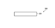
- a semiconductor wafer can be typically mentioned as the substrate 300.
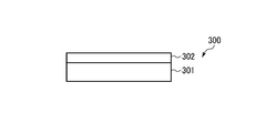
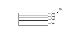
- Examples of the substrate 300 include those shown in FIGS. 2A, 2B, and 2C.
- the substrate 300 is composed only of the semiconductor substrate 301 formed of a semiconductor such as silicon.
- an insulating film 302 such as a SiO 2 film is formed on a semiconductor substrate 301 such as silicon.
- the substrate 300 is a metal such as a Cu film via an insulating film 302 such as a SiO 2 film and a barrier film 303 such as a TaN film, a Ta film, or a TiN film on a semiconductor substrate 301 such as silicon.
- the film 304 is formed.
- the barrier film 303 may be omitted.
- the barrier film 303 may be a laminated film (for example, Ta / TaN).
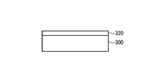
- step 2 the substrate 300 is housed in the processing container, the substrate 300 is heated to a predetermined temperature, and the first processing gas containing the carbon-containing gas is supplied to the substrate 300. As a result, as shown in FIG. 3, a core 310 for forming a graphene structure is formed on the surface of the substrate 300.
- the first process gas used in the step 2 may be only a carbon-containing gas, it may be contained in addition to the hydrogen gas of the carbon-containing gas (H 2 gas). It may also contain a diluting gas or a rare gas as a carrier gas. As the rare gas, Ar, He, Ne, Kr, Xe and the like can be used.
- a highly reactive gas is preferable, and a hydrocarbon gas is preferable.
- hydrocarbon gases those having an unsaturated bond and those having a small number of carbon atoms are more reactive and preferable.
- acetylene (C 2 H 2 ) having a triple bond with 2 carbon atoms ethylene (C 2 H 4 ) having a double bond, and propylene (C 3 H 6 ) having a double bond with 3 carbon atoms. It can be preferably used.
- Hydrocarbons that do not have unsaturated bonds such as methane (CH 4 ), ethane (C 2 H 6 ), and propane (C 3 H 8 ), may be used.
- H 2 gas can be added to control nucleation.
- the formation of graphene proceeds with nucleation and creeping growth based on the following chemical equilibrium equation.
- C x H y ⁇ C (graphene) + H 2 Therefore, the nucleation of graphene can be controlled by adding H 2 gas.
- the temperature of the substrate when carrying out step 2 is preferably 300 to 1000 ° C. More preferably, it is 350 to 750 ° C.
- the pressure in the processing container is preferably in the range of 1.33 to 1330 Pa (0.01 to 10 Torr), more preferably 1.33 to 133 Pa (0.01 to 1 Torr).
- the processing time is preferably 30 sec or more, more preferably 1 to 10 min.
- step 2 By performing the pretreatment in step 2 in this way, nuclei for forming the graphene structure are formed, and the nucleation density is controlled. This makes it possible to improve the coverage of the graphene structure by the plasma CVD of step 3 which is subsequently performed.
- the graphene structure is formed on the substrate 300 as shown in FIG. 4 by causing the plasma of the second processing gas containing the carbon-containing gas to act on the substrate 300 on which the nucleus 310 is formed. Grow 320.
- the plasma at this time is not particularly limited, but it is preferable to use microwave plasma, particularly remote microwave plasma.
- the remote microwave plasma means that a microwave is introduced into a processing container to generate plasma by a microwave electric field, and the plasma is diffused from the plasma generation region to a substrate 300 arranged at a position away from the plasma generation region. A plasma that acts on a plasma.
- the carbon-containing gas can be dissociated into a state suitable for the growth of the graphene structure at a relatively low temperature.
- a rare gas may be used as the second processing gas in addition to the carbon-containing gas used as the film forming raw material.
- the rare gas can be used as a plasma generating gas. That is, microwaves are introduced into the processing container and a plasma generating gas composed of a rare gas is introduced to generate microwave plasma. Then, the carbon-containing gas, which is the film-forming raw material gas, is dissociated by plasma and supplied to the substrate 300 away from the plasma generation region, and the graphene structure 320 is grown on the substrate 300.
- Ar As the rare gas contained in the second processing gas, Ar, He, Ne, Kr, Xe and the like can be used, but among these, Ar capable of stably generating plasma is preferable.
- Examples of the carbon-containing gas contained in the second treatment gas include ethylene (C 2 H 4 ), methane (CH 4 ), ethane (C 2 H 6 ), propane (C 3 H 8 ), and propylene (C 3 H). 6 ) Hydrocarbon gas such as acetylene (C 2 H 2 ) and alcohol gas such as methanol (CH 3 OH) and ethanol (C 2 H 5 OH) can be used.
- the carbon-containing gas used here may be the same as or different from the carbon-containing gas used in step 2.
- the second processing gas may also contain a hydrogen-containing gas, for example, H 2 gas.
- the hydrogen-containing gas can improve the quality of the graphene structure.
- an oxidizing gas such as oxygen gas (O 2 gas) and water vapor (H 2 O gas) may be contained. Defects contained in the graphene structure can be etched with an oxidizing gas to enhance crystallinity.
- the film-forming raw material gas can be introduced at an arbitrary position between the plasma generation region and the region near the substrate, depending on the required degree of dissociation. That is, in the plasma generation region, the degree of dissociation is increased by high-energy plasma, and in the region near the substrate, the degree of dissociation is lower than that in the plasma generation region due to the low electron temperature plasma diffused from the plasma generation region. Therefore, the degree of dissociation of the film-forming raw material gas can be adjusted by the introduction position of the film-forming raw material gas.
- the substrate is arranged in a region away from the microwave plasma generation region, and plasma diffused from the plasma generation region is supplied to the substrate. Therefore, the plasma has a low electron temperature on the substrate, has low damage, and becomes a high-density plasma mainly composed of radicals by microwaves.
- the graphene structure may be only ordinary graphene formed parallel to the substrate, or may contain carbon nanowalls (CNW) grown at an angle with respect to the substrate in addition to graphene.
- CCW carbon nanowalls
- the process conditions are preferably such that the substrate temperature is 350 to 1000 ° C. (more preferably 400 to 800 ° C.) and the microwave power is 100 to 5000 W.
- the pressure in the processing container is 1.33 to 667 Pa (0.01 to 5 Torr) when the surface of the substrate is an insulator and a semiconductor, and 1.33 to 400 Pa (0) when the surface of the substrate is metal. It is preferably 0.01 to 3 Torr).
- the time is preferably in the range of 1 to 200 min.
- the graphene core prior to film formation of the graphene structure by plasma CVD, the graphene core is supplied to the substrate by supplying a gas containing a carbon-containing gas to the substrate while heating the substrate without using plasma. It is possible to form. Therefore, in the subsequent plasma CVD, nucleation and creeping growth are promoted, and a graphene structure having high coverage can be formed. Therefore, it is not necessary to use the activated metal catalyst layer.
- a surface treatment for the purpose of cleaning the surface of the substrate may be performed prior to the pretreatment step of step 2.
- the surface treatment include a treatment of supplying H 2 gas or Ar gas + H 2 gas while heating the substrate to 300 to 600 ° C. At this time, plasma may be generated.
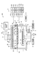
- FIG. 5 is a cross-sectional view schematically showing a first example of the processing apparatus.
- the processing apparatus 100 shown in FIG. 5 is configured as, for example, an RLSA (registered trademark) microwave plasma type plasma processing apparatus.
- the processing device 100 includes a processing container 1, a mounting table 2, a microwave introduction mechanism 3, a gas supply mechanism 4, an exhaust unit 5, and a control unit 6.
- the processing container 1 has a substantially cylindrical shape.
- a circular opening 10 is formed in the substantially central portion of the bottom wall 1a of the processing container 1, and the bottom wall 1a is provided with an exhaust chamber 11 that communicates with the opening 10 and projects downward.
- an exhaust chamber 11 that communicates with the opening 10 and projects downward.
- a carry-in outlet 17 for loading and unloading the wafer W and a gate valve 18 for opening and closing the carry-in outlet 17 are provided on the side wall of the processing container 1.
- the mounting table 2 is provided in the processing container 1 and mounts, for example, a semiconductor wafer (hereinafter, simply referred to as a wafer) W as a substrate.
- the mounting table 2 has a disk shape and is made of ceramics such as AlN, and is supported by a support member 12 made of ceramics such as cylindrical AlN extending upward from the center of the bottom of the exhaust chamber 11.
- a guide ring 13 for guiding the wafer W is provided on the outer edge of the mounting table 2.
- a lifting pin (not shown) for raising and lowering the wafer W is provided so as to be retractable with respect to the upper surface of the mounting table 2.
- a resistance heating type heater 14 is embedded inside the mounting table 2.
- the heater 14 is supplied with power from the heater power supply 15 to heat the wafer W on the mounting table 2 via the mounting table 2. Further, a thermocouple (not shown) is inserted in the mounting table 2, and the heating temperature of the wafer W is controlled to a predetermined temperature in the range of, for example, 300 to 1000 ° C. based on the signal from the thermocouple. It is possible. Further, an electrode 16 having the same size as the wafer W is embedded above the heater 14 in the mounting table 2, and a high frequency bias power supply 19 is electrically connected to the electrode 16. A high frequency bias for drawing ions is applied from the high frequency bias power supply 19 to the mounting table 2. The high frequency bias power supply 19 may not be provided depending on the characteristics of plasma processing.
- the microwave introduction mechanism 3 is for introducing microwaves into the processing container 1, and is provided so as to face the opening at the upper part of the processing container 1.
- the microwave introduction mechanism 3 includes a flat slot antenna 21, a microwave generation unit 22, and a microwave transmission mechanism 23.
- the flat slot antenna 21 is made of, for example, a silver or gold-plated copper plate or aluminum plate on the surface, and is formed so that a plurality of slots 21a for radiating microwaves penetrate in a predetermined pattern.
- the pattern of slot 21a is appropriately set so that microwaves are evenly emitted.
- An example of a suitable pattern is a radial line slot in which two pairs of slots 21a arranged in a T shape are paired and a plurality of pairs of slots 21a are arranged concentrically.
- the length and arrangement spacing of the slots 21a are appropriately determined according to the effective wavelength ( ⁇ g) of the microwave.
- the slot 21a may have another shape such as a circular shape or an arc shape.
- the arrangement form of the slots 21a is not particularly limited, and the slots 21a can be arranged concentrically, for example, spirally or radially.
- the pattern of the slot 21a is appropriately set so as to have microwave radiation characteristics that can obtain a desired plasma density distribution.
- a microwave transmission plate 24 made of a dielectric material is provided so as to be supported by an upper plate 32 provided in a ring shape on the upper part of the processing container 1. Further, a shield member 25 having a water-cooled structure is provided on the flat slot antenna 21. Further, a slow wave material 26 is provided between the shield member 25 and the flat slot antenna 21.
- the slow wave material 26 is made of a dielectric having a dielectric constant larger than that of vacuum, for example, a resin such as quartz, ceramics (Al 2 O 3 ), polytetrafluoroethylene, or polyimide.
- the slow wave material 26 has a function of making the wavelength of the microwave shorter than that in vacuum to make the flat slot antenna 21 smaller.
- the microwave transmission plate 24 is also made of the same dielectric material.
- the thickness of the microwave transmission plate 24 and the slow wave material 26 is adjusted so that the slow wave material 26, the flat slot antenna 21, the microwave transmission plate 24, and the equivalent circuit formed by the plasma satisfy the resonance condition.
- the thickness of the slow wave material 26 the phase of the microwave can be adjusted.
- the thickness so that the junction of the flat slot antenna 21 becomes a "hara" of a standing wave the reflection of the microwave is minimized and the radiant energy of the microwave is maximized. Further, by using the same material for the slow wave material 26 and the microwave transmission plate 24, interfacial reflection of microwaves can be prevented.
- the microwave generation unit 22 is for generating microwaves and has a microwave oscillator.
- the microwave oscillator may be a magnetron or a solid state.
- the frequency of the microwave oscillated from the microwave oscillator can be in the range of 300 MHz to 10 GHz.
- a magnetron as a microwave oscillator, it is possible to oscillate a microwave having a frequency of 2.45 GHz.
- the microwave transmission mechanism 23 is for guiding the microwave from the microwave generating unit 22 to the planar slot antenna 21.
- the microwave transmission mechanism 23 includes a waveguide 27, a coaxial waveguide 28, and a mode conversion mechanism 31.
- the waveguide 27 guides microwaves from the microwave generation unit 22 and extends in the horizontal direction.
- the coaxial waveguide 28 includes an inner conductor 29 extending upward from the center of the planar slot antenna 21 and an outer conductor 30 outside the inner conductor 29.
- the mode conversion mechanism 31 is provided between the waveguide 27 and the coaxial waveguide 28, and is for converting the vibration mode of the microwave.
- the microwave generated by the microwave generating unit 22 propagates in the waveguide 27 in the TE mode, the vibration mode of the microwave is converted from the TE mode to the TEM mode by the mode conversion mechanism 31, and the microwave is transmitted through the coaxial waveguide 28. Is guided to the slow waveguide 26. Then, the microwave is radiated from the slow wave material 26 into the processing container 1 via the slot 21a of the flat slot antenna 21 and the microwave transmission plate 24.
- a tuner (not shown) is provided in the middle of the waveguide 27 to match the impedance of the load (plasma) in the processing container 1 with the characteristic impedance of the power supply of the microwave generating unit 22.
- the gas supply mechanism 4 has a shower plate 41 horizontally provided above the mounting table in the processing container 1 so as to partition the top and bottom, and a ring shape along the inner wall of the processing container 1 at the position above the shower plate 41. It has a shower ring 42 provided in.
- the shower plate 41 includes a gas flow member 51 formed in a grid pattern, a gas flow path 52 provided in a grid pattern inside the gas flow path member 51, and a large number of gases extending downward from the gas flow path 52. It has a discharge hole 53.
- the portion between the lattice-shaped gas passage members 51 is a through hole 54.
- a gas supply path 55 reaching the outer wall of the processing container 1 extends to the gas flow path 52 of the shower plate 41, and a gas supply pipe 56 is connected to the gas supply path 55.
- the gas supply pipe 56 is branched into four branch pipes 56a, 56b, 56c, and 56d.
- the branch pipe 56a, the H 2 gas to supply H 2 gas supply source 57 is connected to a hydrogen-containing gas.
- a C 2 H 2 gas supply source 58a for supplying acetylene (C 2 H 2 ) gas as a carbon-containing gas used for the first processing gas is connected to the branch pipe 56b.
- a C 2 H 4 gas supply source 58 b for supplying ethylene (C 2 H 4 ) gas as a carbon-containing gas used for the second processing gas is connected to the branch pipe 56c.
- the branch pipe 56d, the N 2 gas supply source 59 for supplying N 2 gas used as a purge gas or the like is connected.
- the branch pipes 56a, 56b, 56c, and 56d are provided with a mass flow controller for flow rate control and valves before and after the mass flow controller.
- the shower ring 42 has a ring-shaped gas flow path 66 provided inside the shower ring 42, and a large number of gas discharge holes 67 connected to the gas flow path 66 and opened inside the gas flow path 66. Is connected to the gas supply pipe 61.
- the gas supply pipe 61 is branched into three branch pipes 61a, 61b, and 61c.
- An Ar gas supply source 62 for supplying Ar gas as a rare gas which is a plasma generating gas is connected to the branch pipe 61a.
- An O 2 gas supply source 63 for supplying an O 2 gas which is an oxidizing gas for etching a defect (non-graphene structure) is connected to the branch pipe 61b.
- the branch pipe 61c, N 2 gas supply source 64 for supplying N 2 gas used as a purge gas or the like is connected.
- the branch pipes 61a, 61b, and 61c are provided with a mass flow controller for flow rate control and valves before and after the mass flow controller.
- the carbon-containing gas, oxidizing gas, and rare gas are not limited to those described, and the above-mentioned various gases can be used.
- the exhaust unit 5 is for exhausting the inside of the processing container 1, the exhaust chamber 11, the exhaust pipe 81 provided on the side surface of the exhaust chamber 11, the vacuum pump connected to the exhaust pipe 81, and the pressure control. It has an exhaust device 82 having a valve or the like.
- the control unit 6 typically consists of a computer and controls each unit of the processing device 100.
- the control unit 6 includes a storage unit that stores the process sequence of the processing device 100 and the process recipe that is a control parameter, an input means, a display, and the like, and can perform predetermined control according to the selected process recipe. ..
- the wafer W is carried into the processing container 1 as a substrate and placed on the mounting table 2. If necessary, the surface of the wafer W is cleaned.
- the pressure in the processing container 1 and the wafer temperature are controlled to predetermined values, and the first processing gas containing the carbon-containing gas is supplied to the substrate to perform the pretreatment in step 2.
- the first processing gas Ar gas, which is a rare gas, is supplied from the shower ring 42, and C 2 H 2 gas as a carbon-containing gas is supplied from the shower plate 41. At this time, H 2 gas may be supplied as needed.
- the pretreatment of step 2 forms the core of the graphene structure on the surface of the substrate.
- the pressure in the processing container 1 and the wafer temperature are controlled to predetermined values, and the graphene structure is formed by the remote microwave plasma CVD in step 3.
- Ar gas which is a plasma generating gas
- Ar gas is supplied from the shower ring 42 directly under the microwave transmission plate 24, and the microwave generated by the microwave generating unit 22 is radiated into the processing container 1 to generate plasma. Ignite.
- the microwave generated by the microwave generation unit 22 is guided to the slow wave material 26 via the waveguide 27, the mode conversion mechanism 31, and the coaxial waveguide 28, and is guided from the slow wave material 26 to the slot 21a of the flat slot antenna 21. And it is radiated into the processing container 1 through the microwave transmission plate 24.
- the microwave spreads as a surface wave to the region directly below the microwave transmission plate 24, and surface wave plasma by Ar gas is generated, and that region becomes a plasma generation region.
- C 2 H 4 gas as a carbon-containing gas which is a film-forming raw material gas, is supplied from the shower plate 41.
- H 2 gas and O 2 gas may be supplied as needed.
- These gases are excited and dissociated by the plasma diffused from the plasma generation region, and are supplied to the wafer W, which is a substrate mounted on the mounting table 2 below the shower plate 41.
- the wafer W is arranged in a region away from the plasma generation region, and since the plasma diffused from the plasma generation region is supplied to the wafer W, the plasma becomes low electron temperature plasma on the wafer W and the damage is low. Moreover, it becomes a high-density plasma mainly composed of radicals.
- a graphene structure can be formed on the surface of the substrate on which the nuclei are formed according to a general crystal growth mode of nucleation and creeping growth.
- the C 2 H 4 gas as the carbon-containing gas and, if necessary, the H 2 gas are supplied from the shower plate 41 below the plasma generation region and dissociated by the diffused plasma, so that these gases are excessive. Dissociation can be suppressed.
- these gases may be supplied to the plasma generation region.
- Ar gas which is a plasma generation gas and C 2 H 4 gas which is a carbon-containing gas or the like may be supplied to the plasma generation region to directly ignite the plasma.
- Preferred conditions for remote microwave plasma CVD in the processing apparatus 100 are as follows.
- the wafer surface is an insulator and
- the carbon-containing gas in the first treatment gas and the carbon-containing gas in the second treatment gas may be the same gas, and for example, both C 2 H 2 gas can be used. In that case, the C 2 H 4 gas supply source 58b is unnecessary.
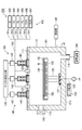
- FIG. 6 is a cross-sectional view schematically showing a second example of the processing apparatus
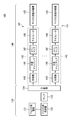
- FIG. 7 is a configuration diagram showing a configuration of a microwave introducing apparatus of the processing apparatus of FIG. 6, and
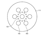
- FIG. 9 is a bottom view schematically showing the top wall portion of the processing container in the processing apparatus of FIG.
- the processing device 200 includes a processing container 101, a mounting table 102, a gas supply mechanism 103, an exhaust device 104, a microwave introduction device 105, and a control unit 106.
- the processing container 101 accommodates the wafer W, is formed of a metal material such as aluminum and an alloy thereof, has a substantially cylindrical shape, and has a plate-shaped top wall portion 111 and a bottom wall portion 113, and these. It has a side wall portion 112 that connects the two.
- the microwave introduction device 105 is provided above the processing container 101 and functions as a plasma generation means for introducing an electromagnetic wave (microwave) into the processing container 101 to generate plasma.
- the microwave introduction device 105 will be described in detail later.
- the top wall portion 111 has a plurality of openings into which the microwave radiation mechanism and the gas introduction portion described later of the microwave introduction device 105 are fitted.
- the side wall portion 112 has a carry-in / out port 114 for carrying in / out the wafer W, which is a substrate, to and from a transport chamber (not shown) adjacent to the processing container 101.
- the carry-in outlet 114 is opened and closed by a gate valve 115.
- An exhaust device 104 is provided on the bottom wall portion 113.
- the exhaust device 104 is provided in an exhaust pipe 116 connected to the bottom wall portion 113, and includes a vacuum pump and a pressure control valve.
- the inside of the processing container 101 is exhausted through the exhaust pipe 116 by the vacuum pump of the exhaust device 104.
- the pressure in the processing container 101 is controlled by the pressure control valve.
- the mounting table 102 is arranged inside the processing container 101 and mounts the wafer W.
- the mounting table 102 has a disk shape and is made of ceramics such as AlN.
- the mounting table 102 is supported by a support member 120 made of ceramics such as cylindrical AlN extending upward from the center of the bottom of the processing container 101.
- a guide ring 181 for guiding the wafer W is provided on the outer edge of the mounting table 102.
- an elevating pin (not shown) for raising and lowering the wafer W is provided so as to be retractable with respect to the upper surface of the mounting table 102.
- a resistance heating type heater 182 is embedded inside the mounting table 102, and the heater 182 heats the wafer W on the mounting table 102 by supplying power from the heater power supply 183.
- a thermocouple (not shown) is inserted in the mounting table 102, and the heating temperature of the wafer W is controlled to a predetermined temperature in the range of, for example, 350 to 1000 ° C. based on the signal from the thermocouple. It is possible.
- an electrode 184 having the same size as the wafer W is embedded above the heater 182 in the mounting table 102, and a high frequency bias power supply 122 is electrically connected to the electrode 184. A high-frequency bias for drawing ions is applied from the high-frequency bias power supply 122 to the mounting table 102.
- the high frequency bias power supply 122 may not be provided depending on the characteristics of plasma processing.
- the gas supply mechanism 103 is for introducing the plasma generation gas and the raw material gas for forming the graphene structure into the processing container 101, and has a plurality of gas introduction nozzles 123.
- the gas introduction nozzle 123 is fitted into an opening formed in the top wall portion 111 of the processing container 101.
- a gas supply pipe 191 is connected to the gas introduction nozzle 123.
- the gas supply pipe 191 is branched into six branch pipes 191a, 191b, 191c, 191d, 191e, and 191f.
- An Ar gas supply source 192 for supplying Ar gas as a rare gas which is a plasma generating gas is connected to the branch pipe 191a.
- the branch pipe 191c, the N 2 gas supply source 194 for supplying a N 2 gas used as a purge gas or the like is connected.
- the branch pipe 191d, the H 2 gas to supply H 2 gas supply source 195 is connected to a hydrogen-containing gas.
- a C 2 H 2 gas supply source 196 for supplying acetylene (C 2 H 2 ) gas as a carbon-containing gas used for the first processing gas is connected to the branch pipe 191e.
- a C 2 H 4 gas supply source 197 that supplies ethylene (C 2 H 4 ) gas as a carbon-containing gas used for the second processing gas is connected to the branch pipe 191 f.
- the branch pipes 191a, 191b, 191c, 191d, 191e, and 191f are provided with a mass flow controller for flow rate control and valves before and after the mass flow controller.
- the shower plate provided C 2 H 4 gas or the like so as to be supplied to a position close to the wafer W to adjust the dissociation of the gas. Further, the same effect can be obtained by extending the nozzle for supplying these gases downward.
- the carbon-containing gas, the oxidizing gas, and the rare gas are not limited to those described, and various gases described above can be used.
- the microwave introduction device 105 is provided above the processing container 101 and functions as a plasma generation means for introducing electromagnetic waves (microwaves) into the processing container 101 to generate plasma.
- the microwave introduction device 105 includes a top wall portion 111 of the processing container 101 that functions as a top plate, a microwave output portion 130, and an antenna unit 140.
- the microwave output unit 130 generates microwaves and distributes and outputs microwaves to a plurality of paths.
- the microwave output unit 130 includes a microwave power supply 131, a microwave oscillator 132, an amplifier 133, and a distributor 134.
- the microwave oscillator 132 is in a solid state and oscillates microwaves (for example, PLL oscillation) at 860 MHz, for example.
- the microwave frequency is not limited to 860 MHz, and those in the range of 700 MHz to 10 GHz such as 2.45 GHz, 8.35 GHz, 5.8 GHz, 1.98 GHz and the like can be used.
- the amplifier 133 amplifies the microwave oscillated by the microwave oscillator 132.
- the distributor 134 distributes the microwave amplified by the amplifier 133 to a plurality of paths, and distributes the microwave while matching the impedances on the input side and the output side.
- the antenna unit 140 introduces the microwave output from the microwave output unit 130 into the processing container 101.
- the antenna unit 140 includes a plurality of antenna modules 141.
- Each of the plurality of antenna modules 141 introduces microwaves distributed by the distributor 134 into the processing container 101.
- the configurations of the plurality of antenna modules 141 are all the same.
- Each antenna module 141 has an amplifier unit 142 that mainly amplifies and outputs the distributed microwaves, and a microwave radiation mechanism 143 that radiates the microwaves output from the amplifier unit 142 into the processing container 101.
- the amplifier unit 142 includes a phase device 145, a variable gain amplifier 146, a main amplifier 147, and an isolator 148.
- the phase device 145 changes the phase of the microwave.
- the variable gain amplifier 146 adjusts the power level of the microwave input to the main amplifier 147.
- the main amplifier 147 is configured as a solid state amplifier.
- the isolator 148 separates the reflected microwaves reflected by the antenna portion of the microwave radiation mechanism 143, which will be described later, toward the main amplifier 147.
- the microwave radiation mechanism 143 includes a coaxial tube 151, a feeding unit 155, a tuner 154, and an antenna unit 156.
- the coaxial tube 151 has an outer conductor 152 forming a tubular shape and an inner conductor 153 provided coaxially with the outer conductor 152 in the outer conductor 152, and has a microwave transmission line between them.
- the power feeding unit 155 feeds the amplified microwave from the amplifier unit 142 to the microwave transmission line.
- Microwaves amplified by the amplifier section 142 by the coaxial cable are introduced into the feeding section 155 from the side of the upper end portion of the outer conductor 152.
- microwave power is supplied to the microwave transmission line between the outer conductor 152 and the inner conductor 153, and the microwave power propagates toward the antenna portion 156.
- the antenna portion 156 radiates microwaves from the coaxial tube 151 into the processing container 101, and is provided at the lower end portion of the coaxial tube 151.
- the antenna portion 156 is arranged on a disk-shaped flat antenna 161 connected to the lower end of the inner conductor 153, a slow wave material 162 arranged on the upper surface side of the flat antenna 161 and a lower surface side of the flat antenna 161. It also has a microwave transmission plate 163.
- the microwave transmission plate 163 is fitted in the top wall portion 111, and the lower surface thereof is exposed in the internal space of the processing container 101.
- the planar antenna 161 has a slot 161a formed so as to penetrate the flat antenna 161. The shape of slot 161a is appropriately set so that microwaves are efficiently radiated.
- a dielectric may be inserted in the slot 161a.
- the slow wave material 162 is made of a material having a dielectric constant larger than that of vacuum, and the phase of the microwave can be adjusted by the thickness thereof so that the radiant energy of the microwave is maximized. it can.
- the microwave transmission plate 163 is also made of a dielectric and has a shape capable of efficiently radiating microwaves in the TE mode. Then, the microwave transmitted through the microwave transmission plate 163 generates plasma in the space inside the processing container 101.
- the material constituting the slow wave material 162 and the microwave transmission plate 163 for example, quartz, ceramics, a fluorine-based resin such as polytetrafluoroethylene resin, a polyimide resin, or the like can be used.
- the tuner 154 matches the impedance of the load with the characteristic impedance of the microwave power supply 131.
- the tuner 154 constitutes a slug tuner.
- the tuner 154 has two slugs 171a and 171b, an actuator 172 that independently drives these two slugs, and a tuner controller 173 that controls the actuator 172. ..
- the slags 171a and 171b are arranged on the base end side (upper end side) of the coaxial tube 151 with respect to the antenna portion 156.
- the slags 171a and 171b are plate-shaped and annular, are made of a dielectric material such as ceramics, and are arranged between the outer conductor 152 and the inner conductor 153 of the coaxial tube 151. Further, the actuator 172 individually drives the slags 171a and 171b by rotating two screws provided inside the inner conductor 153, respectively, in which the slags 171a and 171b are screwed. Then, based on the command from the tuner controller 173, the actuator 172 moves the slags 171a and 171b in the vertical direction. The tuner controller 173 adjusts the positions of the slags 171a and 171b so that the impedance at the end portion becomes 50 ⁇ .
- the main amplifier 147, the tuner 154, and the planar antenna 161 are arranged close to each other.
- the tuner 154 and the planar antenna 161 form a lumped constant circuit and function as a resonator. Although there is an impedance mismatch in the mounting portion of the flat antenna 161, it is tuned directly to the plasma load by the tuner 154, so that it can be tuned with high accuracy including the plasma. Therefore, the influence of reflection on the flat antenna 161 can be eliminated.
- the corresponding microwave transmission plates 163 are arranged evenly in a hexagonal close-packed arrangement. That is, one of the seven microwave transmission plates 163 is arranged in the center of the top wall portion 111, and the other six microwave transmission plates 163 are arranged around the center. These seven microwave transmission plates 163 are arranged so that adjacent microwave transmission plates are evenly spaced. Further, the plurality of nozzles 123 of the gas supply mechanism 103 are arranged so as to surround the periphery of the central microwave transmission plate.
- the arrangement of the microwave radiation mechanism 143 is not limited to this, and the number thereof is not limited to seven.
- the control unit 106 is typically composed of a computer and controls each unit of the processing device 200.
- the control unit 106 includes a storage unit that stores the process sequence of the processing device 200 and the process recipe that is a control parameter, an input means, a display, and the like, and can perform predetermined control according to the selected process recipe. ..
- a wafer W whose surface is made of an insulator, a semiconductor, or a metal as a substrate is carried into the processing container 101. It is placed on the mounting table 102. If necessary, the surface of the wafer W is cleaned.
- the pressure in the processing container 101 and the wafer temperature are controlled to predetermined values, and the first processing gas containing the carbon-containing gas is supplied to the substrate to perform the pretreatment in step 2.
- the first processing gas Ar gas, which is a rare gas, and C 2 H 2 gas as a carbon-containing gas are supplied from the gas introduction nozzle 123. At this time, H 2 gas may be supplied as needed.
- Step 2 forms the core of the graphene structure on the surface of the substrate.
- the pressure in the processing container 101 and the wafer temperature are controlled to predetermined values, and the graphene structure is formed by the remote microwave plasma CVD in step 3.
- Ar gas which is a plasma generating gas
- Ar gas is supplied from the gas introduction nozzle 123 directly below the top wall portion 111 of the processing container 101, and microwaves are radiated into the processing container 101 to ignite the plasma.
- the radiated microwaves are distributed to a plurality of microwaves from the microwave output unit 130 of the microwave introduction device 105 and output, and the microwaves are guided to a plurality of antenna modules 141 of the antenna unit 140 to guide these microwave radiation mechanisms. It was emitted from 143.
- each antenna module 141 microwaves are individually amplified by the main amplifier 147 constituting the solid state amplifier, fed to each microwave radiation mechanism 143, transmitted through the coaxial tube 151, and reach the antenna unit 156.
- the impedance of the microwave is automatically matched by the slugs 171a and 171b of the tuner 154. Therefore, the microwave is radiated from the tuner 154 through the slow wave material 162 of the antenna portion 156 and from the slot 161a of the flat antenna 161 in a state where there is substantially no power reflection.
- the microwave further passes through the microwave transmission plate 163 and is transmitted on the surface (lower surface) of the microwave transmission plate 163 in contact with the plasma to form a surface wave.
- the electric power from each antenna portion 156 is spatially combined in the processing container 101, a surface wave plasma by Ar gas is generated in a region directly below the top wall portion 111, and that region becomes a plasma generation region.
- C 2 H 4 gas as a carbon-containing gas which is a film-forming raw material gas, is supplied from the gas introduction nozzle 123.
- H 2 gas and O 2 gas may be supplied as needed.
- the wafer W which is a substrate mounted on the mounting table 102.
- the wafer W is arranged in a region away from the plasma generation region, and since the plasma diffused from the plasma generation region is supplied to the wafer W, the plasma becomes low electron temperature plasma on the wafer W and the damage is low. Moreover, it becomes a high-density plasma mainly composed of radicals. With such plasma, a graphene structure can be formed according to a general crystal growth mode of nucleation and creeping growth.
- the C 2 H 4 gas as the carbon-containing gas and, if necessary, the H 2 gas are supplied to the plasma generation region and dissociated.
- C 2 H 4 gas and, if necessary, H 2 gas are dissociated by the plasma diffused from the plasma generation region. May be suppressed.
- Ar gas which is a plasma generation gas and C 2 H 4 gas which is a carbon-containing gas or the like may be supplied to the plasma generation region to directly ignite the plasma.
- the microwaves distributed in a plurality of regions are individually amplified by the main amplifier 147 constituting the solid state amplifier, and individually introduced into the processing container 101 from the plurality of antenna units 156 to form a surface wave. After forming, these are combined in space to generate microwave plasma. This eliminates the need for large isolators and synthesizers and is compact. Further, the main amplifier 147, the tuner 154 and the planar antenna 161 are provided in close proximity to each other, and the tuner 154 and the planar antenna 161 form a lumped constant circuit and function as a resonator.
- the tuner 154 can tune the flat slot antenna mounting portion where impedance mismatch exists with high precision including plasma, so that the influence of reflection can be reliably eliminated and high-precision plasma control becomes possible. .. Further, since the plurality of microwave transmission plates 163 are provided, the total area can be reduced as compared with the single microwave transmission plate 24 in the processing apparatus of the first example. Therefore, the microwave power required to stably ignite and discharge the plasma can be reduced.
- the preferable conditions for remote microwave plasma CVD in the processing apparatus 200 are basically the same as those in the first example, but the more preferable conditions differ depending on the item, and are as follows.
- the carbon-containing gas in the first processing gas and the carbon-containing gas in the second processing gas may be the same gas, for example, both of them use C 2 H 2 gas. Can be used. In that case, the C 2 H 4 gas supply source 197 is unnecessary.
- Example 1 a bare Si substrate was prepared as the substrate, and the effect of the pretreatment performed prior to the film formation of the graphene structure by plasma CVD was confirmed.
- the first treatment gas C 2 H 2 gas, H 2 gas, and Ar gas were used, and the flow rates were set to 1 sccm, 0.1 sccm, and 50 sccm, respectively.
- the pressure was 0.4 Torr
- the substrate temperature was 700 ° C.
- the treatment time was changed to 0 sec (no treatment), 180 sec, and 600 sec.
- FIG. 10 is an AFM photograph showing these surface states. As shown in FIG. 10, when the treatment was not performed (0 sec), the surface roughness RMS was 0.095 nm, whereas when the treatment times were 180 sec and 600 sec, the RMS was 0.098 nm and 0.103 nm, respectively. The value of RMS has increased.
- FIG. 11 shows the relationship between the processing time and the RMS value at this time, and as shown in this figure, it can be seen that the RMS value increases as the processing time becomes longer.
- FIG. 12 shows the Raman spectrum of the substrate surface when the processing time is 0 sec, 180 sec, and 600 sec. From FIG. 12, it can be seen that the background intensity of the Raman spectrum increases as the processing time becomes longer. ..
- microcrystals or carbon without a clear structure may be present on the substrate surface by treating with a processing gas containing a carbon-containing gas prior to plasma CVD. ..
- Example 2 a graphene structure was formed by plasma CVD after surface treatment and pretreatment were performed on the Si substrate, which is a substrate, using the processing apparatus of the first example shown in FIG.
- the surface treatment and plasma CVD were carried out under fixed conditions, and the time during the pretreatment was changed.
- FIG. 14 is a diagram showing the relationship between the pretreatment time and the D band intensity (arbitrary unit). As shown in this figure, it was confirmed that the D-band strength, that is, the amount of film formed increased with the increase in the pretreatment time. Further, FIG. 15 shows SEM photographs of the surface when the pretreatment time is 10 sec, 60 sec, and 120 sec, and it can be seen from the SEM photographs that the coverage increases as the pretreatment time increases.
- plasma CVD is not limited to microwave plasma CVD.
- processing device for performing remote microwave plasma CVD is not limited to the above example, and various types of processing devices can be used.
- a substrate for forming a graphene structure a semiconductor wafer based on a semiconductor such as Si has been described as an example, but the present invention is not limited to this.
Abstract
This method for forming a graphene structure includes preparing a substrate, supplying a first treatment gas including a carbon-containing gas to the substrate while heating the substrate, without the use of a plasma, and performing a pre-treatment, and forming a graphene structure on the surface of the substrate by plasma CVD using a plasma of a second treatment gas including a carbon-containing gas.
Description
本開示は、グラフェン構造体を形成する方法および装置に関する。
The present disclosure relates to methods and devices for forming graphene structures.
グラフェンは、1~数十、数百原子層程度のグラファイトの薄膜が基板上に形成されたものである。グラフェン構造体としては、基板に平行に形成された通常のグラフェンの他、数層のグラフェンシートが基板に対して角度をもって典型的には垂直に成長したカーボンナノウォール(以下、CNWとも表記する)が知られている。
Graphene is a thin film of graphite with one to several tens or several hundred atomic layers formed on the substrate. As a graphene structure, in addition to ordinary graphene formed parallel to the substrate, carbon nanowalls in which several layers of graphene sheets are typically grown perpendicular to the substrate at an angle (hereinafter, also referred to as CNW). It has been known.
グラフェンは、炭素原子の共有結合(sp2結合)によって六員環構造の集合体として構成されたものであり、移動度が200000cm2/Vs以上とシリコン(Si)の100倍以上、電流密度が109A/cm2とCuの1000倍以上という特異な電子特性を示す。
Graphene is constructed as an aggregate of a six-membered ring structure by covalent bonds (sp 2- bonds) of carbon atoms, and has a mobility of 200,000 cm 2 / Vs or more, 100 times or more that of silicon (Si), and a current density of 200,000 cm or more. It exhibits a peculiar electronic property of 10 9 A / cm 2 and 1000 times or more that of Cu.
このような特性によりグラフェンは、配線、電界効果トランジスタ(FET)チャネル、バリア膜等、CNWはその構造特性から、燃料電池、電界電子放出源、あるいはセンサ等、種々のデバイス材料として注目されている。
Due to these characteristics, graphene is attracting attention as various device materials such as wiring, field effect transistor (FET) channels, barrier films, etc., and CNW is attracting attention as a fuel cell, field electron emission source, sensor, etc. due to its structural characteristics. ..
グラフェンの形成方法としては、被処理体上に触媒金属層を形成し、触媒金属層の活性化処理を行った後、CVDによりグラフェンを形成するものが提案されおり、特許文献1、2の実施の形態にはCVDの例としてマイクロ波プラズマを用いたCVDが記載されている。
As a method for forming graphene, a method has been proposed in which a catalytic metal layer is formed on an object to be treated, an activation treatment of the catalytic metal layer is performed, and then graphene is formed by CVD. In the form of, CVD using microwave plasma is described as an example of CVD.
本開示は、高い被覆性のグラフェン構造体を形成することができるグラフェン構造体を形成する方法および装置を提供する。
The present disclosure provides methods and devices for forming graphene structures capable of forming highly coated graphene structures.
本開示の一態様に係る方法は、グラフェン構造体を形成する方法であって、基板を準備することと、プラズマを用いずに前記基板を加熱しつつ、炭素含有ガスを含む第1の処理ガスを前記基板に供給して前処理を行うことと、前記前処理後の前記基板の表面に、炭素含有ガスを含む第2の処理ガスのプラズマを用いたプラズマCVDにより前記基板の表面にグラフェン構造体を形成することと、を含む。
A method according to one aspect of the present disclosure is a method for forming a graphene structure, which is a first processing gas containing a carbon-containing gas while preparing a substrate and heating the substrate without using plasma. Is supplied to the substrate for pretreatment, and the surface of the substrate after the pretreatment has a graphene structure on the surface of the substrate by plasma CVD using plasma of a second processing gas containing a carbon-containing gas. Including forming a body.
本開示によれば、高い被覆性のグラフェン構造体を形成することができる。
According to the present disclosure, it is possible to form a graphene structure having high coverage.
以下、添付図面を参照して実施の形態について具体的に説明する。
Hereinafter, the embodiment will be specifically described with reference to the attached drawings.
<グラフェン構造体の形成方法の一実施形態>
最初に、グラフェン構造体の形成方法の一実施形態について説明する。
上述した特許文献1,2では、結晶性の良好なグラフェンを、極力低い温度で効率よく成長させるため、下地としてNi等のグラフェンの成長を促進する触媒となる触媒金属膜を形成し、触媒金属層を、還元性ガスであるH2ガスと窒素含有ガスであるN2ガスのプラズマにより活性化した後、グラフェンをプラズマCVD(PE-CVD)により成長させている。 <One Embodiment of a method for forming a graphene structure>
First, an embodiment of a method for forming a graphene structure will be described.
In Patent Documents 1 and 2 described above, in order to efficiently grow graphene having good crystallinity at an extremely low temperature, a catalyst metal film serving as a catalyst for promoting the growth of graphene such as Ni is formed as a base, and the catalyst metal. After the layer is activated by plasma of H 2 gas which is a reducing gas and N 2 gas which is a nitrogen-containing gas, graphene is grown by plasma CVD (PE-CVD).
最初に、グラフェン構造体の形成方法の一実施形態について説明する。
上述した特許文献1,2では、結晶性の良好なグラフェンを、極力低い温度で効率よく成長させるため、下地としてNi等のグラフェンの成長を促進する触媒となる触媒金属膜を形成し、触媒金属層を、還元性ガスであるH2ガスと窒素含有ガスであるN2ガスのプラズマにより活性化した後、グラフェンをプラズマCVD(PE-CVD)により成長させている。 <One Embodiment of a method for forming a graphene structure>
First, an embodiment of a method for forming a graphene structure will be described.
In
しかし、引用文献1,2には、高い被覆性で基板全面にグラフェンを形成することについては示されていない。
However, References 1 and 2 do not show that graphene is formed on the entire surface of the substrate with high coverage.
一般的なCVDでは、核形成と沿面成長により成膜を進行させるが、このとき核形成密度を制御して被覆性を向上させる手法として、プラズマ前処理等による表面活性化を挙げることができる。
In general CVD, film formation proceeds by nucleation and creeping growth. At this time, surface activation by plasma pretreatment or the like can be mentioned as a method of controlling the nucleation density to improve the coverage.
しかし、プラズマ前処理により十分に表面を活性化しようとすると、同時に下地に対して強いイオンダメージあるいはチャージアップダメージを与えることが予想される。
However, if the surface is sufficiently activated by plasma pretreatment, it is expected that strong ion damage or charge-up damage will be given to the substrate at the same time.
そこで、発明者らが検討した結果、プラズマCVDによるグラフェン構造体の成膜に先立って、プラズマを用いずに基板を加熱しつつ、炭素含有ガスを含むガスを基板に供給する前処理を行うことが有効であることを見出した。
Therefore, as a result of the examination by the inventors, prior to the film formation of the graphene structure by plasma CVD, a pretreatment for supplying a gas containing a carbon-containing gas to the substrate is performed while heating the substrate without using plasma. Found to be valid.
すなわち、グラフェンの成膜の場合、一般的なプラズマ前処理による表面活性化によらなくても、プラズマを用いずに基板を加熱しつつ、炭素含有ガスを含むガスを基板に供給することで核形成が可能であることが見出された。これにより、引き続いて行われるプラズマCVDにおける核形成と沿面成長が促進され、高い被覆性のグラフェン構造体を形成することができる。
That is, in the case of graphene film formation, nucleation is performed by supplying a gas containing a carbon-containing gas to the substrate while heating the substrate without using plasma, without using surface activation by general plasma pretreatment. It was found that the formation is possible. As a result, nucleation and creeping growth in the subsequent plasma CVD are promoted, and a graphene structure having high coverage can be formed.
一実施形態では、上述した特許文献1,2の活性化された金属触媒による触媒反応を利用した技術とは異なり、一般的な結晶の成長様式に従ってグラフェン構造体の成膜反応を進行させることができる。このため、触媒金属層の形成および活性化処理といった煩雑な工程を省略できるという利点もある。
In one embodiment, unlike the technique utilizing the catalytic reaction using the activated metal catalyst of Patent Documents 1 and 2 described above, the film formation reaction of the graphene structure can proceed according to a general crystal growth mode. it can. Therefore, there is an advantage that complicated steps such as formation of the catalyst metal layer and activation treatment can be omitted.
一実施形態のグラフェン構造体の製造方法は、図1に示すように、ステップ1と、ステップ2と、ステップ3とを有する。ステップ1は、基板を準備する工程である。ステップ2は、プラズマを用いずに基板を加熱しつつ、炭素含有ガスを含む第1の処理ガスを基板に供給して前処理を行う工程である。ステップ3は、ステップ2を経た基板の表面に、炭素含有ガスを含む第2の処理ガスを用いたプラズマCVDによりグラフェン構造体を形成する工程である。
As shown in FIG. 1, the method for manufacturing the graphene structure of one embodiment includes step 1, step 2, and step 3. Step 1 is a step of preparing a substrate. Step 2 is a step of supplying a first processing gas containing a carbon-containing gas to the substrate to perform pretreatment while heating the substrate without using plasma. Step 3 is a step of forming a graphene structure on the surface of the substrate that has undergone step 2 by plasma CVD using a second processing gas containing a carbon-containing gas.
ステップ1における基板としては、プラズマCVD成膜ができれば特に制限されないが、一般的なCVDと同様、核形成と沿面成長によりグラフェン構造体の成膜を進行させることができる表面を有するものが好ましい。このような観点から、基板としては、表面がプラズマCVDの際に触媒機能を有さないものが好ましい。具体的には、基板としては、半導体や絶縁体が好適である。また、基板として、プラズマCVD工程の際に表面が触媒機能を有さない金属を用いてもよい。
The substrate in step 1 is not particularly limited as long as plasma CVD film formation can be performed, but a substrate having a surface capable of advancing the film formation of the graphene structure by nucleation and creeping growth is preferable as in general CVD. From this point of view, it is preferable that the substrate does not have a catalytic function during plasma CVD. Specifically, as the substrate, a semiconductor or an insulator is suitable. Further, as the substrate, a metal whose surface does not have a catalytic function during the plasma CVD step may be used.
図2A~図2Cに基板の具体例を示す。基板300としては典型的には半導体ウエハを挙げることができる。基板300としては、図2A、図2B、図2Cに示すものが例示される。図2Aの例では、基板300は、シリコンのような半導体で形成された半導体基体301のみで構成されている。また、図2Bの例では、基板300は、シリコン等の半導体基体301上にSiO2膜のような絶縁膜302が形成されている。図2Cの例では、基板300は、シリコン等の半導体基体301上にSiO2膜のような絶縁膜302およびTaN膜やTa膜、TiN膜等のバリア膜303を介してCu膜のような金属膜304が形成されている。金属によってはバリア膜303を省略してもよい。また、バリア膜303を積層膜(例えばTa/TaN)としてもよい。
Specific examples of the substrate are shown in FIGS. 2A to 2C. A semiconductor wafer can be typically mentioned as the substrate 300. Examples of the substrate 300 include those shown in FIGS. 2A, 2B, and 2C. In the example of FIG. 2A, the substrate 300 is composed only of the semiconductor substrate 301 formed of a semiconductor such as silicon. Further, in the example of FIG. 2B, in the substrate 300, an insulating film 302 such as a SiO 2 film is formed on a semiconductor substrate 301 such as silicon. In the example of FIG. 2C, the substrate 300 is a metal such as a Cu film via an insulating film 302 such as a SiO 2 film and a barrier film 303 such as a TaN film, a Ta film, or a TiN film on a semiconductor substrate 301 such as silicon. The film 304 is formed. Depending on the metal, the barrier film 303 may be omitted. Further, the barrier film 303 may be a laminated film (for example, Ta / TaN).
ステップ2においては、基板300を処理容器内に収容し、基板300を所定温度に加熱しつつ、炭素含有ガスを含む第1の処理ガスを基板300に供給する。これにより、図3に示すように、基板300の表面にグラフェン構造体を形成するための核310が形成される。
In step 2, the substrate 300 is housed in the processing container, the substrate 300 is heated to a predetermined temperature, and the first processing gas containing the carbon-containing gas is supplied to the substrate 300. As a result, as shown in FIG. 3, a core 310 for forming a graphene structure is formed on the surface of the substrate 300.
ステップ2に用いられる第1の処理ガスとしては、炭素含有ガスのみであってもよいし、炭素含有ガスの他に水素ガス(H2ガス)が含まれていてもよい。また、希釈ガスやキャリアガスとしての希ガスを含んでいてもよい。希ガスとしては、Ar、He、Ne、Kr、Xe等を用いることができる。
The first process gas used in the step 2, may be only a carbon-containing gas, it may be contained in addition to the hydrogen gas of the carbon-containing gas (H 2 gas). It may also contain a diluting gas or a rare gas as a carrier gas. As the rare gas, Ar, He, Ne, Kr, Xe and the like can be used.
第1の処理ガスに含まれる炭素含有ガスとしては、反応性の高いものが好ましく、炭化水素ガスが好適である。炭化水素ガスの中でも、不飽和結合を有するものや、炭素数が少ないものが、より反応性が高く好ましい。例えば、炭素数が2で三重結合を有するアセチレン(C2H2)や二重結合を有するエチレン(C2H4)、炭素数が3で二重結合を有するプロピレン(C3H6)を好適に用いることができる。メタン(CH4)、エタン(C2H6)、プロパン(C3H8)のような不飽和結合を有さない炭化水素を用いてもよい。
As the carbon-containing gas contained in the first treatment gas, a highly reactive gas is preferable, and a hydrocarbon gas is preferable. Among the hydrocarbon gases, those having an unsaturated bond and those having a small number of carbon atoms are more reactive and preferable. For example, acetylene (C 2 H 2 ) having a triple bond with 2 carbon atoms, ethylene (C 2 H 4 ) having a double bond, and propylene (C 3 H 6 ) having a double bond with 3 carbon atoms. It can be preferably used. Hydrocarbons that do not have unsaturated bonds, such as methane (CH 4 ), ethane (C 2 H 6 ), and propane (C 3 H 8 ), may be used.
H2ガスは、核形成を制御するために添加することができる。プラズマCVDによるグラフェンの成膜においては、以下のような化学平衡式に基づいて、核形成と沿面成長をともなってグラフェンの成膜が進行する。
CxHy⇔C(graphene)+H2
したがって、H2ガスを添加することにより、グラフェンの核形成を制御することができる。 H 2 gas can be added to control nucleation. In the formation of graphene by plasma CVD, the formation of graphene proceeds with nucleation and creeping growth based on the following chemical equilibrium equation.
C x H y ⇔C (graphene) +H 2
Therefore, the nucleation of graphene can be controlled by adding H 2 gas.
CxHy⇔C(graphene)+H2
したがって、H2ガスを添加することにより、グラフェンの核形成を制御することができる。 H 2 gas can be added to control nucleation. In the formation of graphene by plasma CVD, the formation of graphene proceeds with nucleation and creeping growth based on the following chemical equilibrium equation.
C x H y ⇔C (graphene) +
Therefore, the nucleation of graphene can be controlled by adding H 2 gas.
H2ガスの添加量は、核生成促進の観点から、炭素含有ガスに対して、体積比率で300%以下であることが好ましい。
Amount of H 2 gas, from the viewpoint of nucleation promoting, it is preferred for the carbon-containing gas, 300% or less by volume ratio.
ステップ2を実施する際の基板の温度は、300~1000℃が好ましい。より好ましくは、350~750℃である。また、処理容器内の圧力は、1.33~1330Pa(0.01~10Torr)の範囲が好ましく、1.33~133Pa(0.01~1Torr)がより好ましい。また、処理時間は30sec以上が好ましく、1~10minがより好ましい。
The temperature of the substrate when carrying out step 2 is preferably 300 to 1000 ° C. More preferably, it is 350 to 750 ° C. The pressure in the processing container is preferably in the range of 1.33 to 1330 Pa (0.01 to 10 Torr), more preferably 1.33 to 133 Pa (0.01 to 1 Torr). The processing time is preferably 30 sec or more, more preferably 1 to 10 min.
このようにステップ2の前処理が行われることにより、グラフェン構造体を形成するための核が形成され、核形成密度が制御される。これにより、引き続き行われるステップ3のプラズマCVDによるグラフェン構造体の被覆性を向上させることができる。
By performing the pretreatment in step 2 in this way, nuclei for forming the graphene structure are formed, and the nucleation density is controlled. This makes it possible to improve the coverage of the graphene structure by the plasma CVD of step 3 which is subsequently performed.
次のステップ3においては、核310が形成された基板300に対し、炭素含有ガスを含む第2の処理ガスのプラズマを作用させることにより、図4に示すように、基板300上にグラフェン構造体320を成長させる。
In the next step 3, the graphene structure is formed on the substrate 300 as shown in FIG. 4 by causing the plasma of the second processing gas containing the carbon-containing gas to act on the substrate 300 on which the nucleus 310 is formed. Grow 320.
このときのプラズマは特に限定されないが、マイクロ波プラズマ、特に、リモートマイクロ波プラズマを用いることが好ましい。本開示において、リモートマイクロ波プラズマとは、処理容器内にマイクロ波を導入してマイクロ波電界によりプラズマを生成し、プラズマ生成領域から離れた位置に配置された基板300にプラズマ生成領域から拡散したプラズマを作用させるプラズマをいう。リモートマイクロ波プラズマを用いることにより比較的低温で炭素含有ガスをグラフェン構造体の成長に適した状態に解離させることができる。
The plasma at this time is not particularly limited, but it is preferable to use microwave plasma, particularly remote microwave plasma. In the present disclosure, the remote microwave plasma means that a microwave is introduced into a processing container to generate plasma by a microwave electric field, and the plasma is diffused from the plasma generation region to a substrate 300 arranged at a position away from the plasma generation region. A plasma that acts on a plasma. By using the remote microwave plasma, the carbon-containing gas can be dissociated into a state suitable for the growth of the graphene structure at a relatively low temperature.
この場合、第2の処理ガスとして、成膜原料として用いられる炭素含有ガスの他に希ガスを用いてもよい。希ガスはプラズマ生成ガスとして用いることができる。すなわち、処理容器内にマイクロ波を導入するとともに希ガスからなるプラズマ生成ガスを導入して、マイクロ波プラズマを生成する。そして、成膜原料ガスである炭素含有ガスをプラズマにより解離させてプラズマ生成領域から離れた基板300に供給し、基板300上にグラフェン構造体320を成長させる。
In this case, a rare gas may be used as the second processing gas in addition to the carbon-containing gas used as the film forming raw material. The rare gas can be used as a plasma generating gas. That is, microwaves are introduced into the processing container and a plasma generating gas composed of a rare gas is introduced to generate microwave plasma. Then, the carbon-containing gas, which is the film-forming raw material gas, is dissociated by plasma and supplied to the substrate 300 away from the plasma generation region, and the graphene structure 320 is grown on the substrate 300.
第2の処理ガスに含まれる希ガスとしては、Ar、He、Ne、Kr、Xe等を用いることができるが、これらの中ではプラズマを安定に生成できるArが好ましい。
As the rare gas contained in the second processing gas, Ar, He, Ne, Kr, Xe and the like can be used, but among these, Ar capable of stably generating plasma is preferable.
第2の処理ガスに含まれる炭素含有ガスとしては、例えばエチレン(C2H4)、メタン(CH4)、エタン(C2H6)、プロパン(C3H8)、プロピレン(C3H6)、アセチレン(C2H2)等の炭化水素ガス、メタノール(CH3OH)、エタノール(C2H5OH)等のアルコールガスを用いることができる。なお、ここで用いられる炭素含有ガスは、ステップ2で用いられる炭素含有ガスと同じでも異なっていてもよい。
Examples of the carbon-containing gas contained in the second treatment gas include ethylene (C 2 H 4 ), methane (CH 4 ), ethane (C 2 H 6 ), propane (C 3 H 8 ), and propylene (C 3 H). 6 ) Hydrocarbon gas such as acetylene (C 2 H 2 ) and alcohol gas such as methanol (CH 3 OH) and ethanol (C 2 H 5 OH) can be used. The carbon-containing gas used here may be the same as or different from the carbon-containing gas used in step 2.
第2の処理ガスとしては、その他に、水素含有ガス、例えばH2ガスを含んでいてもよい。水素含有ガスにより、グラフェン構造体の品質を向上させることができる。また、酸化性ガス、例えば酸素ガス(O2ガス)、水蒸気(H2Oガス)を含んでいてもよい。酸化性ガスによりグラフェン構造体に含まれる欠陥をエッチングして結晶性を高めることができる。
The second processing gas may also contain a hydrogen-containing gas, for example, H 2 gas. The hydrogen-containing gas can improve the quality of the graphene structure. Further, an oxidizing gas such as oxygen gas (O 2 gas) and water vapor (H 2 O gas) may be contained. Defects contained in the graphene structure can be etched with an oxidizing gas to enhance crystallinity.
リモートマイクロ波プラズマを用いる場合は、必要とされる解離度に応じて、成膜原料ガスを、プラズマ生成領域と基板近傍領域の間の任意の位置に導入することができる。すなわち、プラズマ生成領域では高エネルギーのプラズマにより解離度が高くなり、基板の近傍領域ではプラズマ生成領域から拡散した低電子温度のプラズマにより、プラズマ生成領域よりも解離度が低くなる。このため、成膜原料ガスの導入位置により成膜原料ガスの解離度を調整することができる。
When remote microwave plasma is used, the film-forming raw material gas can be introduced at an arbitrary position between the plasma generation region and the region near the substrate, depending on the required degree of dissociation. That is, in the plasma generation region, the degree of dissociation is increased by high-energy plasma, and in the region near the substrate, the degree of dissociation is lower than that in the plasma generation region due to the low electron temperature plasma diffused from the plasma generation region. Therefore, the degree of dissociation of the film-forming raw material gas can be adjusted by the introduction position of the film-forming raw material gas.
また、リモートマイクロ波プラズマCVDを用いる場合は、基板は、マイクロ波プラズマ生成領域から離れた領域に配置されており、基板へは、プラズマ生成領域から拡散したプラズマが供給される。このため、基板上では低電子温度のプラズマとなり低ダメージであり、かつマイクロ波によりラジカル主体の高密度のプラズマとなる。
Further, when remote microwave plasma CVD is used, the substrate is arranged in a region away from the microwave plasma generation region, and plasma diffused from the plasma generation region is supplied to the substrate. Therefore, the plasma has a low electron temperature on the substrate, has low damage, and becomes a high-density plasma mainly composed of radicals by microwaves.
グラフェン構造体としては、基板に平行に形成された通常のグラフェンのみであってもよいし、グラフェンに加えて基板に対して角度をもって成長したカーボンナノウォール(CNW)を含んでいてもよい。
The graphene structure may be only ordinary graphene formed parallel to the substrate, or may contain carbon nanowalls (CNW) grown at an angle with respect to the substrate in addition to graphene.
リモートマイクロ波プラズマを用いた場合のプロセス条件としては、基板の温度が350~1000℃(より好ましくは400~800℃)、マイクロ波パワーが100~5000Wであることが好ましい。また、処理容器内の圧力は、基板の表面が絶縁体および半導体の場合は、1.33~667Pa(0.01~5Torr)、基板の表面が金属の場合は、1.33~400Pa(0.01~3Torr)であることが好ましい。時間は1~200minの範囲が好ましい。
When the remote microwave plasma is used, the process conditions are preferably such that the substrate temperature is 350 to 1000 ° C. (more preferably 400 to 800 ° C.) and the microwave power is 100 to 5000 W. The pressure in the processing container is 1.33 to 667 Pa (0.01 to 5 Torr) when the surface of the substrate is an insulator and a semiconductor, and 1.33 to 400 Pa (0) when the surface of the substrate is metal. It is preferably 0.01 to 3 Torr). The time is preferably in the range of 1 to 200 min.
本実施形態によれば、プラズマCVDによるグラフェン構造体の成膜に先立って、プラズマを用いずに基板を加熱しつつ、炭素含有ガスを含むガスを基板に供給することにより、基板にグラフェンの核を形成することが可能である。このため、引き続いて行われるプラズマCVDにおいて、核形成と沿面成長が促進され、高い被覆性のグラフェン構造体を形成することができる。したがって、活性化処理された金属触媒層は用いなくてもよい。
According to this embodiment, prior to film formation of the graphene structure by plasma CVD, the graphene core is supplied to the substrate by supplying a gas containing a carbon-containing gas to the substrate while heating the substrate without using plasma. It is possible to form. Therefore, in the subsequent plasma CVD, nucleation and creeping growth are promoted, and a graphene structure having high coverage can be formed. Therefore, it is not necessary to use the activated metal catalyst layer.
また、このように、核形成と沿面成長という一般的な結晶の成長様式に従ってグラフェン構造体を形成するので、上述した特許文献1,2の活性化された金属触媒による触媒反応を利用する必要はない。
Further, since the graphene structure is formed according to the general crystal growth mode of nucleation and creeping growth in this way, it is necessary to utilize the catalytic reaction by the activated metal catalyst of Patent Documents 1 and 2 described above. Absent.
なお、ステップ2の前処理工程に先立って、基板表面の清浄化を目的とした表面処理を行ってもよい。表面処理としては、基板を300~600℃に加熱しつつ、例えばH2ガスまたはArガス+H2ガスを供給する処理を挙げることができる。この際にプラズマを生成してもよい。
Prior to the pretreatment step of step 2, a surface treatment for the purpose of cleaning the surface of the substrate may be performed. Examples of the surface treatment include a treatment of supplying H 2 gas or Ar gas + H 2 gas while heating the substrate to 300 to 600 ° C. At this time, plasma may be generated.
<処理装置>
次に、上記実施形態に係るグラフェン構造体の形成方法の実施に好適な処理装置の例について説明する。 <Processing device>
Next, an example of a processing apparatus suitable for carrying out the method for forming a graphene structure according to the above embodiment will be described.
次に、上記実施形態に係るグラフェン構造体の形成方法の実施に好適な処理装置の例について説明する。 <Processing device>
Next, an example of a processing apparatus suitable for carrying out the method for forming a graphene structure according to the above embodiment will be described.
[処理装置の第1の例]
図5は、処理装置の第1の例を模式的に示す断面図である。図5に示す処理装置100は、例えばRLSA(登録商標)マイクロ波プラズマ方式のプラズマ処理装置として構成される。 [First example of processing device]
FIG. 5 is a cross-sectional view schematically showing a first example of the processing apparatus. Theprocessing apparatus 100 shown in FIG. 5 is configured as, for example, an RLSA (registered trademark) microwave plasma type plasma processing apparatus.
図5は、処理装置の第1の例を模式的に示す断面図である。図5に示す処理装置100は、例えばRLSA(登録商標)マイクロ波プラズマ方式のプラズマ処理装置として構成される。 [First example of processing device]
FIG. 5 is a cross-sectional view schematically showing a first example of the processing apparatus. The
この処理装置100は、処理容器1と、載置台2と、マイクロ波導入機構3と、ガス供給機構4と、排気部5と、制御部6とを有している。
The processing device 100 includes a processing container 1, a mounting table 2, a microwave introduction mechanism 3, a gas supply mechanism 4, an exhaust unit 5, and a control unit 6.
処理容器1は略円筒状をなしている。処理容器1の底壁1aの略中央部には円形の開口部10が形成されており、底壁1aにはこの開口部10と連通し、下方に向けて突出する排気室11が設けられている。処理容器1の側壁には、ウエハWを搬入出するための搬入出口17と、この搬入出口17を開閉するゲートバルブ18とが設けられている。
The processing container 1 has a substantially cylindrical shape. A circular opening 10 is formed in the substantially central portion of the bottom wall 1a of the processing container 1, and the bottom wall 1a is provided with an exhaust chamber 11 that communicates with the opening 10 and projects downward. There is. On the side wall of the processing container 1, a carry-in outlet 17 for loading and unloading the wafer W and a gate valve 18 for opening and closing the carry-in outlet 17 are provided.
載置台2は、処理容器1内に設けられ、基板として例えば半導体ウエハ(以下単にウエハと記す)Wを載置する。載置台2は、円板状をなし、AlN等のセラミックスからなっており、排気室11の底部中央から上方に延びる円筒状のAlN等のセラミックスからなる支持部材12により支持されている。載置台2の外縁部にはウエハWをガイドするためのガイドリング13が設けられている。また、載置台2の内部には、ウエハWを昇降するための昇降ピン(図示せず)が載置台2の上面に対して突没可能に設けられている。さらに、載置台2の内部には抵抗加熱型のヒータ14が埋め込まれている。このヒータ14は、ヒータ電源15から給電されることにより、載置台2を介してその上のウエハWを加熱する。また、載置台2には、熱電対(図示せず)が挿入されており、熱電対からの信号に基づいて、ウエハWの加熱温度を、例えば300~1000℃の範囲の所定の温度に制御可能となっている。さらに、載置台2内のヒータ14の上方には、ウエハWと同程度の大きさの電極16が埋設されており、この電極16には、高周波バイアス電源19が電気的に接続されている。この高周波バイアス電源19から載置台2に、イオンを引き込むための高周波バイアスが印加される。なお、高周波バイアス電源19はプラズマ処理の特性によっては設けなくてもよい。
The mounting table 2 is provided in the processing container 1 and mounts, for example, a semiconductor wafer (hereinafter, simply referred to as a wafer) W as a substrate. The mounting table 2 has a disk shape and is made of ceramics such as AlN, and is supported by a support member 12 made of ceramics such as cylindrical AlN extending upward from the center of the bottom of the exhaust chamber 11. A guide ring 13 for guiding the wafer W is provided on the outer edge of the mounting table 2. Further, inside the mounting table 2, a lifting pin (not shown) for raising and lowering the wafer W is provided so as to be retractable with respect to the upper surface of the mounting table 2. Further, a resistance heating type heater 14 is embedded inside the mounting table 2. The heater 14 is supplied with power from the heater power supply 15 to heat the wafer W on the mounting table 2 via the mounting table 2. Further, a thermocouple (not shown) is inserted in the mounting table 2, and the heating temperature of the wafer W is controlled to a predetermined temperature in the range of, for example, 300 to 1000 ° C. based on the signal from the thermocouple. It is possible. Further, an electrode 16 having the same size as the wafer W is embedded above the heater 14 in the mounting table 2, and a high frequency bias power supply 19 is electrically connected to the electrode 16. A high frequency bias for drawing ions is applied from the high frequency bias power supply 19 to the mounting table 2. The high frequency bias power supply 19 may not be provided depending on the characteristics of plasma processing.
マイクロ波導入機構3は、処理容器1内にマイクロ波を導入するためのものであり、処理容器1の上部の開口部に臨むように設けられている。マイクロ波導入機構3は、平面スロットアンテナ21と、マイクロ波発生部22と、マイクロ波伝送機構23とを有している。
The microwave introduction mechanism 3 is for introducing microwaves into the processing container 1, and is provided so as to face the opening at the upper part of the processing container 1. The microwave introduction mechanism 3 includes a flat slot antenna 21, a microwave generation unit 22, and a microwave transmission mechanism 23.
平面スロットアンテナ21は、例えば表面が銀または金メッキされた銅板またはアルミニウム板からなり、マイクロ波を放射するための複数のスロット21aが所定パターンで貫通するように形成された構成となっている。スロット21aのパターンは、マイクロ波が均等に放射されるように適宜設定される。好適なパターンの例としては、T字状に配置された2つのスロット21aを一対として複数対のスロット21aが同心円状に配置されているラジアルラインスロットを挙げることができる。スロット21aの長さや配列間隔は、マイクロ波の実効波長(λg)に応じて適宜決定される。また、スロット21aは、円形状、円弧状等の他の形状であってもよい。さらに、スロット21aの配置形態は特に限定されず、同心円状のほか、例えば、螺旋状、放射状に配置することもできる。スロット21aのパターンは、所望のプラズマ密度分布が得られるマイクロ波放射特性となるように、適宜設定される。
The flat slot antenna 21 is made of, for example, a silver or gold-plated copper plate or aluminum plate on the surface, and is formed so that a plurality of slots 21a for radiating microwaves penetrate in a predetermined pattern. The pattern of slot 21a is appropriately set so that microwaves are evenly emitted. An example of a suitable pattern is a radial line slot in which two pairs of slots 21a arranged in a T shape are paired and a plurality of pairs of slots 21a are arranged concentrically. The length and arrangement spacing of the slots 21a are appropriately determined according to the effective wavelength (λg) of the microwave. Further, the slot 21a may have another shape such as a circular shape or an arc shape. Further, the arrangement form of the slots 21a is not particularly limited, and the slots 21a can be arranged concentrically, for example, spirally or radially. The pattern of the slot 21a is appropriately set so as to have microwave radiation characteristics that can obtain a desired plasma density distribution.
平面スロットアンテナ21の下方には誘電体からなるマイクロ波透過板24が処理容器1の上部にリング状に設けられたアッパープレート32に支持されるように設けられている。また、平面スロットアンテナ21の上には水冷構造のシールド部材25が設けられている。さらに、シールド部材25と平面スロットアンテナ21との間には、遅波材26が設けられている。
Below the flat slot antenna 21, a microwave transmission plate 24 made of a dielectric material is provided so as to be supported by an upper plate 32 provided in a ring shape on the upper part of the processing container 1. Further, a shield member 25 having a water-cooled structure is provided on the flat slot antenna 21. Further, a slow wave material 26 is provided between the shield member 25 and the flat slot antenna 21.
遅波材26は、真空よりも大きい誘電率を有する誘電体、例えば石英、セラミックス(Al2O3)、ポリテトラフルオロエチレン、ポリイミドなどの樹脂からなる。遅波材26はマイクロ波の波長を真空中より短くして平面スロットアンテナ21を小さくする機能を有している。なお、マイクロ波透過板24も同様の誘電体で構成されている。
The slow wave material 26 is made of a dielectric having a dielectric constant larger than that of vacuum, for example, a resin such as quartz, ceramics (Al 2 O 3 ), polytetrafluoroethylene, or polyimide. The slow wave material 26 has a function of making the wavelength of the microwave shorter than that in vacuum to make the flat slot antenna 21 smaller. The microwave transmission plate 24 is also made of the same dielectric material.
マイクロ波透過板24および遅波材26の厚さは、遅波材26、平面スロットアンテナ21、マイクロ波透過板24、およびプラズマで形成される等価回路が共振条件を満たすように調整される。遅波材26の厚さを調整することにより、マイクロ波の位相を調整することができる。平面スロットアンテナ21の接合部が定在波の「はら」になるように厚さを調整することにより、マイクロ波の反射が極小化され、マイクロ波の放射エネルギーが最大となる。また、遅波材26とマイクロ波透過板24を同じ材質とすることにより、マイクロ波の界面反射を防止することができる。
The thickness of the microwave transmission plate 24 and the slow wave material 26 is adjusted so that the slow wave material 26, the flat slot antenna 21, the microwave transmission plate 24, and the equivalent circuit formed by the plasma satisfy the resonance condition. By adjusting the thickness of the slow wave material 26, the phase of the microwave can be adjusted. By adjusting the thickness so that the junction of the flat slot antenna 21 becomes a "hara" of a standing wave, the reflection of the microwave is minimized and the radiant energy of the microwave is maximized. Further, by using the same material for the slow wave material 26 and the microwave transmission plate 24, interfacial reflection of microwaves can be prevented.
マイクロ波発生部22は、マイクロ波を発生させるためのものであり、マイクロ波発振器を有している。マイクロ波発振器は、マグネトロンであってもソリッドステートであってもよい。マイクロ波発振器から発振されるマイクロ波の周波数は、300MHz~10GHzの範囲を用いることができる。例えば、マイクロ波発振器としてマグネトロンを用いることにより周波数が2.45GHzのマイクロ波を発振することができる。
The microwave generation unit 22 is for generating microwaves and has a microwave oscillator. The microwave oscillator may be a magnetron or a solid state. The frequency of the microwave oscillated from the microwave oscillator can be in the range of 300 MHz to 10 GHz. For example, by using a magnetron as a microwave oscillator, it is possible to oscillate a microwave having a frequency of 2.45 GHz.
マイクロ波伝送機構23は、マイクロ波発生部22からのマイクロ波を平面スロットアンテナ21に導くためのものである。マイクロ波伝送機構23は、導波管27と、同軸導波管28と、モード変換機構31とを有している。導波管27は、マイクロ波発生部22からマイクロ波を導くものであり、水平方向に延びている。同軸導波管28は、平面スロットアンテナ21の中心から上方に伸びる内導体29およびその外側の外導体30からなる。モード変換機構31は、導波管27と同軸導波管28との間に設けられ、マイクロ波の振動モードを変換するためのものである。マイクロ波発生部22で発生したマイクロ波は、TEモードで導波管27を伝播し、モード変換機構31でマイクロ波の振動モードがTEモードからTEMモードへ変換され、同軸導波管28を介して遅波材26に導かれる。そして、マイクロ波は、遅波材26から平面スロットアンテナ21のスロット21aおよびマイクロ波透過板24を経て処理容器1内に放射される。なお、導波管27の途中には、処理容器1内の負荷(プラズマ)のインピーダンスをマイクロ波発生部22の電源の特性インピーダンスに整合させるチューナ(図示せず)が設けられている。
The microwave transmission mechanism 23 is for guiding the microwave from the microwave generating unit 22 to the planar slot antenna 21. The microwave transmission mechanism 23 includes a waveguide 27, a coaxial waveguide 28, and a mode conversion mechanism 31. The waveguide 27 guides microwaves from the microwave generation unit 22 and extends in the horizontal direction. The coaxial waveguide 28 includes an inner conductor 29 extending upward from the center of the planar slot antenna 21 and an outer conductor 30 outside the inner conductor 29. The mode conversion mechanism 31 is provided between the waveguide 27 and the coaxial waveguide 28, and is for converting the vibration mode of the microwave. The microwave generated by the microwave generating unit 22 propagates in the waveguide 27 in the TE mode, the vibration mode of the microwave is converted from the TE mode to the TEM mode by the mode conversion mechanism 31, and the microwave is transmitted through the coaxial waveguide 28. Is guided to the slow waveguide 26. Then, the microwave is radiated from the slow wave material 26 into the processing container 1 via the slot 21a of the flat slot antenna 21 and the microwave transmission plate 24. A tuner (not shown) is provided in the middle of the waveguide 27 to match the impedance of the load (plasma) in the processing container 1 with the characteristic impedance of the power supply of the microwave generating unit 22.
ガス供給機構4は、処理容器1内の載置台の上方位置に上下を仕切るように水平に設けられたシャワープレート41と、シャワープレート41の上方位置に、処理容器1の内壁に沿ってリング状に設けられたシャワーリング42とを有している。
The gas supply mechanism 4 has a shower plate 41 horizontally provided above the mounting table in the processing container 1 so as to partition the top and bottom, and a ring shape along the inner wall of the processing container 1 at the position above the shower plate 41. It has a shower ring 42 provided in.
シャワープレート41は、格子状に形成されたガス通流部材51と、このガス通流部材51の内部に格子状に設けられたガス流路52と、ガス流路52から下方に延びる多数のガス吐出孔53とを有している。格子状のガス通流部材51の間の部分は貫通孔54となっている。このシャワープレート41のガス流路52には処理容器1の外壁に達するガス供給路55が延びており、このガス供給路55にはガス供給配管56が接続されている。このガス供給配管56は分岐管56a、56b、56c、56dの4つに分岐している。分岐管56aには、水素含有ガスであるH2ガスを供給するH2ガス供給源57が接続されている。分岐管56bには、第1の処理ガスに用いられる炭素含有ガスとしてのアセチレン(C2H2)ガスを供給するC2H2ガス供給源58aが接続されている。分岐管56cには、第2の処理ガスに用いられる炭素含有ガスとしてのエチレン(C2H4)ガスを供給するC2H4ガス供給源58bが接続されている。分岐管56dには、パージガス等として用いられるN2ガスを供給するN2ガス供給源59が接続されている。なお、分岐管56a、56b、56c、56dには、図示してはいないが、流量制御用のマスフローコントローラおよびその前後のバルブが設けられている。
The shower plate 41 includes a gas flow member 51 formed in a grid pattern, a gas flow path 52 provided in a grid pattern inside the gas flow path member 51, and a large number of gases extending downward from the gas flow path 52. It has a discharge hole 53. The portion between the lattice-shaped gas passage members 51 is a through hole 54. A gas supply path 55 reaching the outer wall of the processing container 1 extends to the gas flow path 52 of the shower plate 41, and a gas supply pipe 56 is connected to the gas supply path 55. The gas supply pipe 56 is branched into four branch pipes 56a, 56b, 56c, and 56d. The branch pipe 56a, the H 2 gas to supply H 2 gas supply source 57 is connected to a hydrogen-containing gas. A C 2 H 2 gas supply source 58a for supplying acetylene (C 2 H 2 ) gas as a carbon-containing gas used for the first processing gas is connected to the branch pipe 56b. A C 2 H 4 gas supply source 58 b for supplying ethylene (C 2 H 4 ) gas as a carbon-containing gas used for the second processing gas is connected to the branch pipe 56c. The branch pipe 56d, the N 2 gas supply source 59 for supplying N 2 gas used as a purge gas or the like is connected. Although not shown, the branch pipes 56a, 56b, 56c, and 56d are provided with a mass flow controller for flow rate control and valves before and after the mass flow controller.
シャワーリング42は、その内部に設けられたリング状のガス流路66と、このガス流路66に接続されその内側に開口する多数のガス吐出孔67とを有しており、ガス流路にはガス供給配管61が接続されている。このガス供給配管61は分岐管61a、61b、61cの3つに分岐している。分岐管61aには、プラズマ生成ガスである希ガスとしてのArガスを供給するArガス供給源62が接続されている。分岐管61bには、欠陥(非グラフェン構造体)をエッチングするための酸化性ガスであるO2ガスを供給するO2ガス供給源63が接続されている。分岐管61cには、パージガス等として用いられるN2ガスを供給するN2ガス供給源64が接続されている。分岐管61a、61b、61cには、図示してはいないが、流量制御用のマスフローコントローラおよびその前後のバルブが設けられている。なお、炭素含有ガス、酸化性ガス、希ガスは、記載されたものに限定されず、上述した種々のガスを用いることができる。
The shower ring 42 has a ring-shaped gas flow path 66 provided inside the shower ring 42, and a large number of gas discharge holes 67 connected to the gas flow path 66 and opened inside the gas flow path 66. Is connected to the gas supply pipe 61. The gas supply pipe 61 is branched into three branch pipes 61a, 61b, and 61c. An Ar gas supply source 62 for supplying Ar gas as a rare gas which is a plasma generating gas is connected to the branch pipe 61a. An O 2 gas supply source 63 for supplying an O 2 gas which is an oxidizing gas for etching a defect (non-graphene structure) is connected to the branch pipe 61b. The branch pipe 61c, N 2 gas supply source 64 for supplying N 2 gas used as a purge gas or the like is connected. Although not shown, the branch pipes 61a, 61b, and 61c are provided with a mass flow controller for flow rate control and valves before and after the mass flow controller. The carbon-containing gas, oxidizing gas, and rare gas are not limited to those described, and the above-mentioned various gases can be used.
排気部5は、処理容器1内を排気するためのものであり、上記排気室11と、排気室11の側面に設けられた排気配管81と、排気配管81に接続された真空ポンプおよび圧力制御バルブ等を有する排気装置82とを有する。
The exhaust unit 5 is for exhausting the inside of the processing container 1, the exhaust chamber 11, the exhaust pipe 81 provided on the side surface of the exhaust chamber 11, the vacuum pump connected to the exhaust pipe 81, and the pressure control. It has an exhaust device 82 having a valve or the like.
制御部6は、典型的にはコンピュータからなり、処理装置100の各部を制御するようになっている。制御部6は処理装置100のプロセスシーケンスおよび制御パラメータであるプロセスレシピを記憶した記憶部や、入力手段およびディスプレイ等を備えており、選択されたプロセスレシピに従って所定の制御を行うことが可能である。
The control unit 6 typically consists of a computer and controls each unit of the processing device 100. The control unit 6 includes a storage unit that stores the process sequence of the processing device 100 and the process recipe that is a control parameter, an input means, a display, and the like, and can perform predetermined control according to the selected process recipe. ..
このように構成される処理装置100により上記実施形態に従ってグラフェン構造体を形成するに際しては、まず、処理容器1内に基板としてウエハWを搬入し、載置台2の上に載置する。必要に応じてウエハWの表面の清浄化を行う。
When forming a graphene structure according to the above embodiment by the processing device 100 configured in this way, first, the wafer W is carried into the processing container 1 as a substrate and placed on the mounting table 2. If necessary, the surface of the wafer W is cleaned.
この清浄化処理の好ましい条件は以下のとおりである。
ガス流量:Ar/H2=0~2000/10~2000sccm
圧力:0.1~10Torr(13.3~1333Pa)
ウエハ温度:300~600℃
時間:10~120min The preferred conditions for this cleaning treatment are as follows.
Gas flow rate: Ar / H 2 = 0 to 2000/10 to 2000 sccm
Pressure: 0.1 to 10 Torr (13.3 to 1333 Pa)
Wafer temperature: 300-600 ° C
Time: 10-120 min
ガス流量:Ar/H2=0~2000/10~2000sccm
圧力:0.1~10Torr(13.3~1333Pa)
ウエハ温度:300~600℃
時間:10~120min The preferred conditions for this cleaning treatment are as follows.
Gas flow rate: Ar / H 2 = 0 to 2000/10 to 2000 sccm
Pressure: 0.1 to 10 Torr (13.3 to 1333 Pa)
Wafer temperature: 300-600 ° C
Time: 10-120 min
次いで、処理容器1内の圧力およびウエハ温度を所定の値に制御し、炭素含有ガスを含む第1の処理ガスを基板に供給して、ステップ2の前処理を行う。具体的には、第1の処理ガスとして、シャワーリング42から希ガスであるArガスを供給するとともに、シャワープレート41から炭素含有ガスとしてのC2H2ガスを供給する。このとき、必要に応じてH2ガスを供給してもよい。ステップ2の前処理により基板の表面にグラフェン構造体の核が形成される。
Next, the pressure in the processing container 1 and the wafer temperature are controlled to predetermined values, and the first processing gas containing the carbon-containing gas is supplied to the substrate to perform the pretreatment in step 2. Specifically, as the first processing gas, Ar gas, which is a rare gas, is supplied from the shower ring 42, and C 2 H 2 gas as a carbon-containing gas is supplied from the shower plate 41. At this time, H 2 gas may be supplied as needed. The pretreatment of step 2 forms the core of the graphene structure on the surface of the substrate.
このステップ2の前処理の際の好ましい条件は、以下のとおりである。
ガス流量:
Arガス=0~1000sccm
C2H2ガス=0.1~100sccm
H2ガス=0~300sccm
圧力:1.33~133Pa(0.01~1Torr)
温度:300~1000℃(より好ましくは350~750℃)
時間:1~10min The preferable conditions for the pretreatment instep 2 are as follows.
Gas flow rate:
Ar gas = 0 to 1000 sccm
C 2 H 2 gas = 0.1-100 sccm
H 2 gas = 0 ~ 300sccm
Pressure: 1.33 to 133 Pa (0.01 to 1 Torr)
Temperature: 300-1000 ° C (more preferably 350-750 ° C)
Time: 1-10 min
ガス流量:
Arガス=0~1000sccm
C2H2ガス=0.1~100sccm
H2ガス=0~300sccm
圧力:1.33~133Pa(0.01~1Torr)
温度:300~1000℃(より好ましくは350~750℃)
時間:1~10min The preferable conditions for the pretreatment in
Gas flow rate:
Ar gas = 0 to 1000 sccm
C 2 H 2 gas = 0.1-100 sccm
H 2 gas = 0 ~ 300sccm
Pressure: 1.33 to 133 Pa (0.01 to 1 Torr)
Temperature: 300-1000 ° C (more preferably 350-750 ° C)
Time: 1-10 min
次いで、処理容器1内の圧力およびウエハ温度を所定の値に制御し、ステップ3のリモートマイクロ波プラズマCVDによるグラフェン構造体の形成を行う。
Next, the pressure in the processing container 1 and the wafer temperature are controlled to predetermined values, and the graphene structure is formed by the remote microwave plasma CVD in step 3.
具体的には、シャワーリング42から、プラズマ生成ガスであるArガスをマイクロ波透過板24の直下に供給するとともに、マイクロ波発生部22で発生したマイクロ波を処理容器1内に放射させ、プラズマを着火する。マイクロ波発生部22で発生したマイクロ波は、導波管27、モード変換機構31、同軸導波管28を介して遅波材26に導かれ、遅波材26から平面スロットアンテナ21のスロット21aおよびマイクロ波透過板24を経て処理容器1内に放射される。
Specifically, Ar gas, which is a plasma generating gas, is supplied from the shower ring 42 directly under the microwave transmission plate 24, and the microwave generated by the microwave generating unit 22 is radiated into the processing container 1 to generate plasma. Ignite. The microwave generated by the microwave generation unit 22 is guided to the slow wave material 26 via the waveguide 27, the mode conversion mechanism 31, and the coaxial waveguide 28, and is guided from the slow wave material 26 to the slot 21a of the flat slot antenna 21. And it is radiated into the processing container 1 through the microwave transmission plate 24.
マイクロ波は、表面波としてマイクロ波透過板24の直下領域に広がり、Arガスによる表面波プラズマが生成され、その領域がプラズマ生成領域となる。
The microwave spreads as a surface wave to the region directly below the microwave transmission plate 24, and surface wave plasma by Ar gas is generated, and that region becomes a plasma generation region.
そして、プラズマが着火したタイミングでシャワープレート41から成膜原料ガスである炭素含有ガスとしてのC2H4ガスを供給する。このとき、必要に応じてH2ガス、O2ガスを供給してもよい。
Then, at the timing when the plasma is ignited, C 2 H 4 gas as a carbon-containing gas, which is a film-forming raw material gas, is supplied from the shower plate 41. At this time, H 2 gas and O 2 gas may be supplied as needed.
これらのガスはプラズマ生成領域から拡散したプラズマにより励起されて解離し、シャワープレート41の下方の載置台2上に載置された基板であるウエハWに供給される。ウエハWは、プラズマ生成領域とは離れた領域に配置されており、ウエハWへは、プラズマ生成領域から拡散したプラズマが供給されるため、ウエハW上では低電子温度のプラズマとなり低ダメージであり、かつラジカル主体の高密度のプラズマとなる。このようなプラズマにより、核が形成された基板の表面に、核形成と沿面成長という、一般的な結晶の成長様式に従ってグラフェン構造体を形成することができる。
These gases are excited and dissociated by the plasma diffused from the plasma generation region, and are supplied to the wafer W, which is a substrate mounted on the mounting table 2 below the shower plate 41. The wafer W is arranged in a region away from the plasma generation region, and since the plasma diffused from the plasma generation region is supplied to the wafer W, the plasma becomes low electron temperature plasma on the wafer W and the damage is low. Moreover, it becomes a high-density plasma mainly composed of radicals. By such plasma, a graphene structure can be formed on the surface of the substrate on which the nuclei are formed according to a general crystal growth mode of nucleation and creeping growth.
このとき、炭素含有ガスとしてのC2H4ガスおよび必要に応じてH2ガスは、シャワープレート41からプラズマ生成領域の下方に供給され、拡散したプラズマにより解離されるので、これらガスが過度に解離することを抑制することができる。ただし、これらガスをプラズマ生成領域に供給してもよい。また、プラズマ生成ガスであるArガスは用いなくともよく、炭素含有ガスであるC2H4ガス等をプラズマ生成領域に供給して直接プラズマを着火してもよい。
At this time, the C 2 H 4 gas as the carbon-containing gas and, if necessary, the H 2 gas are supplied from the shower plate 41 below the plasma generation region and dissociated by the diffused plasma, so that these gases are excessive. Dissociation can be suppressed. However, these gases may be supplied to the plasma generation region. Further, it is not necessary to use Ar gas which is a plasma generation gas, and C 2 H 4 gas which is a carbon-containing gas or the like may be supplied to the plasma generation region to directly ignite the plasma.
処理装置100におけるリモートマイクロ波プラズマCVDの際の好ましい条件は、以下のとおりである。
ガス流量:
Arガス=0~2000sccm
C2H4ガス=0.1~300sccm
O2ガス=0~10sccm
H2ガス=0~500sccm
圧力:
ウエハ表面が絶縁体および半導体の場合
1.33~667Pa(0.01~5Torr)
ウエハ表面が金属の場合(触媒機能なし)
1.33~400Pa(0.01~3Torr)
温度:350~1000℃(より好ましくは400~800℃)
マイクロ波パワー:100~5000W(より好ましくは1000~3500W)
時間:1~200min Preferred conditions for remote microwave plasma CVD in theprocessing apparatus 100 are as follows.
Gas flow rate:
Ar gas = 0-2000 sccm
C 2 H 4 gas = 0.1-300 sccm
O 2 gas = 0 to 10 sccm
H 2 gas = 0 ~ 500sccm
pressure:
When the wafer surface is an insulator and a semiconductor 1.33 to 667 Pa (0.01 to 5 Torr)
When the wafer surface is metal (no catalyst function)
1.33 to 400 Pa (0.01 to 3 Torr)
Temperature: 350-1000 ° C (more preferably 400-800 ° C)
Microwave power: 100-5000W (more preferably 1000-3500W)
Time: 1-200 min
ガス流量:
Arガス=0~2000sccm
C2H4ガス=0.1~300sccm
O2ガス=0~10sccm
H2ガス=0~500sccm
圧力:
ウエハ表面が絶縁体および半導体の場合
1.33~667Pa(0.01~5Torr)
ウエハ表面が金属の場合(触媒機能なし)
1.33~400Pa(0.01~3Torr)
温度:350~1000℃(より好ましくは400~800℃)
マイクロ波パワー:100~5000W(より好ましくは1000~3500W)
時間:1~200min Preferred conditions for remote microwave plasma CVD in the
Gas flow rate:
Ar gas = 0-2000 sccm
C 2 H 4 gas = 0.1-300 sccm
O 2 gas = 0 to 10 sccm
H 2 gas = 0 ~ 500sccm
pressure:
When the wafer surface is an insulator and a semiconductor 1.33 to 667 Pa (0.01 to 5 Torr)
When the wafer surface is metal (no catalyst function)
1.33 to 400 Pa (0.01 to 3 Torr)
Temperature: 350-1000 ° C (more preferably 400-800 ° C)
Microwave power: 100-5000W (more preferably 1000-3500W)
Time: 1-200 min
なお、第1の処理ガス中の炭素含有ガスと第2の処理ガス中の炭素含有ガスとは、同じガスであってもよく、例えば両者ともC2H2ガスを用いることができる。その場合には、C2H4ガス供給源58bは不要である。
The carbon-containing gas in the first treatment gas and the carbon-containing gas in the second treatment gas may be the same gas, and for example, both C 2 H 2 gas can be used. In that case, the C 2 H 4 gas supply source 58b is unnecessary.
[処理装置の第2の例]
図6は、処理装置の第2の例を模式的に示す断面図、図7は図6の処理装置のマイクロ波導入装置の構成を示す構成図、図8は図6の処理装置におけるマイクロ波放射機構を模式的に示す断面図、図9は図6の処理装置における処理容器の天壁部を模式的に示す底面図である。 [Second example of processing device]
FIG. 6 is a cross-sectional view schematically showing a second example of the processing apparatus, FIG. 7 is a configuration diagram showing a configuration of a microwave introducing apparatus of the processing apparatus of FIG. 6, and FIG. A cross-sectional view schematically showing the radiation mechanism, FIG. 9 is a bottom view schematically showing the top wall portion of the processing container in the processing apparatus of FIG.
この処理装置200は、処理容器101と、載置台102と、ガス供給機構103と、排気装置104と、マイクロ波導入装置105と、制御部106とを備えている。
The processing device 200 includes a processing container 101, a mounting table 102, a gas supply mechanism 103, an exhaust device 104, a microwave introduction device 105, and a control unit 106.
処理容器101は、ウエハWを収容するものであり、例えばアルミニウムおよびその合金等の金属材料によって形成され、略円筒形状をなしており、板状の天壁部111および底壁部113と、これらを連結する側壁部112とを有している。マイクロ波導入装置105は、処理容器101の上部に設けられ、処理容器101内に電磁波(マイクロ波)を導入してプラズマを生成するプラズマ生成手段として機能する。マイクロ波導入装置105については後で詳細に説明する。
The processing container 101 accommodates the wafer W, is formed of a metal material such as aluminum and an alloy thereof, has a substantially cylindrical shape, and has a plate-shaped top wall portion 111 and a bottom wall portion 113, and these. It has a side wall portion 112 that connects the two. The microwave introduction device 105 is provided above the processing container 101 and functions as a plasma generation means for introducing an electromagnetic wave (microwave) into the processing container 101 to generate plasma. The microwave introduction device 105 will be described in detail later.
天壁部111には、マイクロ波導入装置105の後述するマイクロ波放射機構およびガス導入部が嵌め込まれる複数の開口部を有している。側壁部112は、処理容器101に隣接する搬送室(図示せず)との間で基板であるウエハWの搬入出を行うための搬入出口114を有している。搬入出口114はゲートバルブ115により開閉されるようになっている。底壁部113には排気装置104が設けられている。排気装置104は底壁部113に接続された排気管116に設けられ、真空ポンプと圧力制御バルブを備えている。排気装置104の真空ポンプにより排気管116を介して処理容器101内が排気される。処理容器101内の圧力は圧力制御バルブにより制御される。
The top wall portion 111 has a plurality of openings into which the microwave radiation mechanism and the gas introduction portion described later of the microwave introduction device 105 are fitted. The side wall portion 112 has a carry-in / out port 114 for carrying in / out the wafer W, which is a substrate, to and from a transport chamber (not shown) adjacent to the processing container 101. The carry-in outlet 114 is opened and closed by a gate valve 115. An exhaust device 104 is provided on the bottom wall portion 113. The exhaust device 104 is provided in an exhaust pipe 116 connected to the bottom wall portion 113, and includes a vacuum pump and a pressure control valve. The inside of the processing container 101 is exhausted through the exhaust pipe 116 by the vacuum pump of the exhaust device 104. The pressure in the processing container 101 is controlled by the pressure control valve.
載置台102は、処理容器101の内部に配置され、ウエハWを載置する。載置台102は、円板状をなしており、AlN等のセラミックスからなっている。載置台102は、処理容器101の底部中央から上方に延びる円筒状のAlN等のセラミックスからなる支持部材120により支持されている。載置台102の外縁部にはウエハWをガイドするためのガイドリング181が設けられている。また、載置台102の内部には、ウエハWを昇降するための昇降ピン(図示せず)が載置台102の上面に対して突没可能に設けられている。さらに、載置台102の内部には抵抗加熱型のヒータ182が埋め込まれており、このヒータ182はヒータ電源183から給電されることにより載置台102を介してその上のウエハWを加熱する。また、載置台102には、熱電対(図示せず)が挿入されており、熱電対からの信号に基づいて、ウエハWの加熱温度を、例えば350~1000℃の範囲の所定の温度に制御可能となっている。さらに、載置台102内のヒータ182の上方には、ウエハWと同程度の大きさの電極184が埋設されており、この電極184には、高周波バイアス電源122が電気的に接続されている。この高周波バイアス電源122から載置台102に、イオンを引き込むための高周波バイアスが印加される。なお、高周波バイアス電源122はプラズマ処理の特性によっては設けなくてもよい。
The mounting table 102 is arranged inside the processing container 101 and mounts the wafer W. The mounting table 102 has a disk shape and is made of ceramics such as AlN. The mounting table 102 is supported by a support member 120 made of ceramics such as cylindrical AlN extending upward from the center of the bottom of the processing container 101. A guide ring 181 for guiding the wafer W is provided on the outer edge of the mounting table 102. Further, inside the mounting table 102, an elevating pin (not shown) for raising and lowering the wafer W is provided so as to be retractable with respect to the upper surface of the mounting table 102. Further, a resistance heating type heater 182 is embedded inside the mounting table 102, and the heater 182 heats the wafer W on the mounting table 102 by supplying power from the heater power supply 183. Further, a thermocouple (not shown) is inserted in the mounting table 102, and the heating temperature of the wafer W is controlled to a predetermined temperature in the range of, for example, 350 to 1000 ° C. based on the signal from the thermocouple. It is possible. Further, an electrode 184 having the same size as the wafer W is embedded above the heater 182 in the mounting table 102, and a high frequency bias power supply 122 is electrically connected to the electrode 184. A high-frequency bias for drawing ions is applied from the high-frequency bias power supply 122 to the mounting table 102. The high frequency bias power supply 122 may not be provided depending on the characteristics of plasma processing.
ガス供給機構103は、プラズマ生成ガス、およびグラフェン構造体を形成するための原料ガスを処理容器101内に導入するためのものであり、複数のガス導入ノズル123を有している。ガス導入ノズル123は、処理容器101の天壁部111に形成された開口部に嵌め込まれている。ガス導入ノズル123には、ガス供給配管191が接続されている。このガス供給配管191は分岐管191a、191b、191c、191d、191e、191fの6つに分岐している。分岐管191aには、プラズマ生成ガスである希ガスとしてのArガスを供給するArガス供給源192が接続されている。分岐管191bには、酸化性ガスであるO2ガスを供給するO2ガス供給源193が接続されている。分岐管191cには、パージガス等として用いられるN2ガスを供給するN2ガス供給源194が接続されている。分岐管191dには、水素含有ガスであるH2ガスを供給するH2ガス供給源195が接続されている。分岐管191eには、第1の処理ガスに用いられる炭素含有ガスとしてのアセチレン(C2H2)ガスを供給するC2H2ガス供給源196が接続されている。分岐管191fには、第2の処理ガスに用いられる炭素含有ガスとしてのエチレン(C2H4)ガスを供給するC2H4ガス供給源197が接続されている。なお、分岐管191a、191b、191c、191d、191e、191fには、図示してはいないが、流量制御用のマスフローコントローラおよびその前後のバルブが設けられている。なお、第1の例と同様にシャワープレートを設けてC2H4ガス等をウエハWに近い位置に供給するようにしてガスの解離を調整することもできる。また、これらのガスを供給するノズルを下方に延ばすことにより同様の効果を得ることができる。さらに、第1の例と同様、炭素含有ガス、酸化性ガス、希ガスは、記載されたものに限定されず、上述した種々のガスを用いることができる。
The gas supply mechanism 103 is for introducing the plasma generation gas and the raw material gas for forming the graphene structure into the processing container 101, and has a plurality of gas introduction nozzles 123. The gas introduction nozzle 123 is fitted into an opening formed in the top wall portion 111 of the processing container 101. A gas supply pipe 191 is connected to the gas introduction nozzle 123. The gas supply pipe 191 is branched into six branch pipes 191a, 191b, 191c, 191d, 191e, and 191f. An Ar gas supply source 192 for supplying Ar gas as a rare gas which is a plasma generating gas is connected to the branch pipe 191a. An O 2 gas supply source 193 that supplies an O 2 gas, which is an oxidizing gas, is connected to the branch pipe 191b. The branch pipe 191c, the N 2 gas supply source 194 for supplying a N 2 gas used as a purge gas or the like is connected. The branch pipe 191d, the H 2 gas to supply H 2 gas supply source 195 is connected to a hydrogen-containing gas. A C 2 H 2 gas supply source 196 for supplying acetylene (C 2 H 2 ) gas as a carbon-containing gas used for the first processing gas is connected to the branch pipe 191e. A C 2 H 4 gas supply source 197 that supplies ethylene (C 2 H 4 ) gas as a carbon-containing gas used for the second processing gas is connected to the branch pipe 191 f. Although not shown, the branch pipes 191a, 191b, 191c, 191d, 191e, and 191f are provided with a mass flow controller for flow rate control and valves before and after the mass flow controller. It is also possible to the first embodiment as well as the shower plate provided C 2 H 4 gas or the like so as to be supplied to a position close to the wafer W to adjust the dissociation of the gas. Further, the same effect can be obtained by extending the nozzle for supplying these gases downward. Further, as in the first example, the carbon-containing gas, the oxidizing gas, and the rare gas are not limited to those described, and various gases described above can be used.
マイクロ波導入装置105は、前述のように、処理容器101の上方に設けられ、処理容器101内に電磁波(マイクロ波)を導入してプラズマを生成するプラズマ生成手段として機能する。図6に示すように、マイクロ波導入装置105は、天板として機能する処理容器101の天壁部111と、マイクロ波出力部130と、アンテナユニット140とを有する。
As described above, the microwave introduction device 105 is provided above the processing container 101 and functions as a plasma generation means for introducing electromagnetic waves (microwaves) into the processing container 101 to generate plasma. As shown in FIG. 6, the microwave introduction device 105 includes a top wall portion 111 of the processing container 101 that functions as a top plate, a microwave output portion 130, and an antenna unit 140.
マイクロ波出力部130は、マイクロ波を生成するとともに、マイクロ波を複数の経路に分配して出力するものである。マイクロ波出力部130は、図7に示すように、マイクロ波電源131と、マイクロ波発振器132と、アンプ133と、分配器134とを有している。マイクロ波発振器132はソリッドステートであり、例えば、860MHzでマイクロ波を発振(例えば、PLL発振)させる。なお、マイクロ波の周波数は、860MHzに限らず、2.45GHz、8.35GHz、5.8GHz、1.98GHz等、700MHzから10GHzの範囲のものを用いることができる。アンプ133は、マイクロ波発振器132によって発振されたマイクロ波を増幅するものである。分配器134は、アンプ133によって増幅されたマイクロ波を複数の経路に分配するものであり、入力側と出力側のインピーダンスを整合させながらマイクロ波を分配する。
The microwave output unit 130 generates microwaves and distributes and outputs microwaves to a plurality of paths. As shown in FIG. 7, the microwave output unit 130 includes a microwave power supply 131, a microwave oscillator 132, an amplifier 133, and a distributor 134. The microwave oscillator 132 is in a solid state and oscillates microwaves (for example, PLL oscillation) at 860 MHz, for example. The microwave frequency is not limited to 860 MHz, and those in the range of 700 MHz to 10 GHz such as 2.45 GHz, 8.35 GHz, 5.8 GHz, 1.98 GHz and the like can be used. The amplifier 133 amplifies the microwave oscillated by the microwave oscillator 132. The distributor 134 distributes the microwave amplified by the amplifier 133 to a plurality of paths, and distributes the microwave while matching the impedances on the input side and the output side.
アンテナユニット140は、マイクロ波出力部130から出力されたマイクロ波を処理容器101に導入するものである。アンテナユニット140は、図7に示すように、複数のアンテナモジュール141を含んでいる。複数のアンテナモジュール141は、それぞれ、分配器134によって分配されたマイクロ波を処理容器101内に導入する。複数のアンテナモジュール141の構成は全て同一である。各アンテナモジュール141は、分配されたマイクロ波を主に増幅して出力するアンプ部142と、アンプ部142から出力されたマイクロ波を処理容器101内に放射するマイクロ波放射機構143とを有する。
The antenna unit 140 introduces the microwave output from the microwave output unit 130 into the processing container 101. As shown in FIG. 7, the antenna unit 140 includes a plurality of antenna modules 141. Each of the plurality of antenna modules 141 introduces microwaves distributed by the distributor 134 into the processing container 101. The configurations of the plurality of antenna modules 141 are all the same. Each antenna module 141 has an amplifier unit 142 that mainly amplifies and outputs the distributed microwaves, and a microwave radiation mechanism 143 that radiates the microwaves output from the amplifier unit 142 into the processing container 101.
アンプ部142は、位相器145と、可変ゲインアンプ146と、メインアンプ147と、アイソレータ148とを有する。位相器145は、マイクロ波の位相を変化させる。可変ゲインアンプ146は、メインアンプ147に入力されるマイクロ波の電力レベルを調整する。メインアンプ147は、ソリッドステートアンプとして構成される。アイソレータ148は、後述するマイクロ波放射機構143のアンテナ部で反射されてメインアンプ147に向かう反射マイクロ波を分離する。
The amplifier unit 142 includes a phase device 145, a variable gain amplifier 146, a main amplifier 147, and an isolator 148. The phase device 145 changes the phase of the microwave. The variable gain amplifier 146 adjusts the power level of the microwave input to the main amplifier 147. The main amplifier 147 is configured as a solid state amplifier. The isolator 148 separates the reflected microwaves reflected by the antenna portion of the microwave radiation mechanism 143, which will be described later, toward the main amplifier 147.
図6に示すように、複数のマイクロ波放射機構143は、天壁部111に設けられている。また、マイクロ波放射機構143は、図8に示すように、同軸管151と、給電部155と、チューナ154と、アンテナ部156とを有する。同軸管151は、筒状をなす外側導体152および外側導体152内に外側導体152と同軸状に設けられた内側導体153を有し、それらの間にマイクロ波伝送路を有する。
As shown in FIG. 6, a plurality of microwave radiation mechanisms 143 are provided on the top wall portion 111. Further, as shown in FIG. 8, the microwave radiation mechanism 143 includes a coaxial tube 151, a feeding unit 155, a tuner 154, and an antenna unit 156. The coaxial tube 151 has an outer conductor 152 forming a tubular shape and an inner conductor 153 provided coaxially with the outer conductor 152 in the outer conductor 152, and has a microwave transmission line between them.
給電部155は、アンプ部142からの増幅されたマイクロ波をマイクロ波伝送路に給電するものである。給電部155には、外側導体152の上端部の側方から同軸ケーブルによりアンプ部142で増幅されたマイクロ波が導入される。例えば、給電アンテナによりマイクロ波を放射することにより外側導体152と内側導体153との間のマイクロ波伝送路にマイクロ波電力が給電され、マイクロ波電力がアンテナ部156に向かって伝播する。
The power feeding unit 155 feeds the amplified microwave from the amplifier unit 142 to the microwave transmission line. Microwaves amplified by the amplifier section 142 by the coaxial cable are introduced into the feeding section 155 from the side of the upper end portion of the outer conductor 152. For example, by radiating microwaves from the feeding antenna, microwave power is supplied to the microwave transmission line between the outer conductor 152 and the inner conductor 153, and the microwave power propagates toward the antenna portion 156.
アンテナ部156は、同軸管151からのマイクロ波を処理容器101内に放射するものであり、同軸管151の下端部に設けられている。アンテナ部156は、内側導体153の下端部に接続された円板状をなす平面アンテナ161と、平面アンテナ161の上面側に配置された遅波材162と、平面アンテナ161の下面側に配置されたマイクロ波透過板163とを有している。マイクロ波透過板163は天壁部111に嵌め込まれており、その下面は処理容器101の内部空間に露出している。平面アンテナ161は、貫通するように形成されたスロット161aを有している。スロット161aの形状は、マイクロ波が効率良く放射されるように適宜設定される。スロット161aには誘電体が挿入されていてもよい。遅波材162は、真空よりも大きい誘電率を有する材料によって形成されており、その厚さによりマイクロ波の位相を調整することができ、マイクロ波の放射エネルギーが最大となるようにすることができる。マイクロ波透過板163も誘電体で構成されマイクロ波をTEモードで効率的に放射することができるような形状をなしている。そして、マイクロ波透過板163を透過したマイクロ波は、処理容器101内の空間にプラズマを生成する。遅波材162およびマイクロ波透過板163を構成する材料としては、例えば、石英やセラミックス、ポリテトラフルオロエチレン樹脂等のフッ素系樹脂、ポリイミド樹脂等を用いることができる。
The antenna portion 156 radiates microwaves from the coaxial tube 151 into the processing container 101, and is provided at the lower end portion of the coaxial tube 151. The antenna portion 156 is arranged on a disk-shaped flat antenna 161 connected to the lower end of the inner conductor 153, a slow wave material 162 arranged on the upper surface side of the flat antenna 161 and a lower surface side of the flat antenna 161. It also has a microwave transmission plate 163. The microwave transmission plate 163 is fitted in the top wall portion 111, and the lower surface thereof is exposed in the internal space of the processing container 101. The planar antenna 161 has a slot 161a formed so as to penetrate the flat antenna 161. The shape of slot 161a is appropriately set so that microwaves are efficiently radiated. A dielectric may be inserted in the slot 161a. The slow wave material 162 is made of a material having a dielectric constant larger than that of vacuum, and the phase of the microwave can be adjusted by the thickness thereof so that the radiant energy of the microwave is maximized. it can. The microwave transmission plate 163 is also made of a dielectric and has a shape capable of efficiently radiating microwaves in the TE mode. Then, the microwave transmitted through the microwave transmission plate 163 generates plasma in the space inside the processing container 101. As the material constituting the slow wave material 162 and the microwave transmission plate 163, for example, quartz, ceramics, a fluorine-based resin such as polytetrafluoroethylene resin, a polyimide resin, or the like can be used.
チューナ154は、負荷のインピーダンスをマイクロ波電源131の特性インピーダンスに整合させるものである。チューナ154は、スラグチューナを構成している。例えば図8に示すように、チューナ154は、2つのスラグ171a、171bと、これら2つのスラグをそれぞれ独立して駆動するアクチュエータ172と、このアクチュエータ172を制御するチューナコントローラ173とを有している。スラグ171a、171bは、同軸管151のアンテナ部156よりも基端部側(上端部側)の部分に配置されている。
The tuner 154 matches the impedance of the load with the characteristic impedance of the microwave power supply 131. The tuner 154 constitutes a slug tuner. For example, as shown in FIG. 8, the tuner 154 has two slugs 171a and 171b, an actuator 172 that independently drives these two slugs, and a tuner controller 173 that controls the actuator 172. .. The slags 171a and 171b are arranged on the base end side (upper end side) of the coaxial tube 151 with respect to the antenna portion 156.
スラグ171a,171bは、板状かつ環状をなし、セラミックス等の誘電体材料で構成され、同軸管151の外側導体152と内側導体153の間に配置されている。また、アクチュエータ172は、例えば、内側導体153の内部に設けられた、それぞれスラグ171a,171bが螺号する2本のねじを回転させることによりスラグ171a,171bを個別に駆動する。そして、チューナコントローラ173からの指令に基づいて、アクチュエータ172によって、スラグ171a,171bを上下方向に移動させる。チューナコントローラ173は、終端部のインピーダンスが50Ωになるように、スラグ171a,171bの位置を調整する。
The slags 171a and 171b are plate-shaped and annular, are made of a dielectric material such as ceramics, and are arranged between the outer conductor 152 and the inner conductor 153 of the coaxial tube 151. Further, the actuator 172 individually drives the slags 171a and 171b by rotating two screws provided inside the inner conductor 153, respectively, in which the slags 171a and 171b are screwed. Then, based on the command from the tuner controller 173, the actuator 172 moves the slags 171a and 171b in the vertical direction. The tuner controller 173 adjusts the positions of the slags 171a and 171b so that the impedance at the end portion becomes 50Ω.
メインアンプ147と、チューナ154と、平面アンテナ161とは近接配置している。そして、チューナ154と平面アンテナ161とは集中定数回路を構成し、かつ共振器として機能する。平面アンテナ161の取り付け部分には、インピーダンス不整合が存在するが、チューナ154によりプラズマ負荷に対して直接チューニングするので、プラズマを含めて高精度でチューニングすることができる。このため、平面アンテナ161における反射の影響を解消することができる。
The main amplifier 147, the tuner 154, and the planar antenna 161 are arranged close to each other. The tuner 154 and the planar antenna 161 form a lumped constant circuit and function as a resonator. Although there is an impedance mismatch in the mounting portion of the flat antenna 161, it is tuned directly to the plasma load by the tuner 154, so that it can be tuned with high accuracy including the plasma. Therefore, the influence of reflection on the flat antenna 161 can be eliminated.
図9に示すように、本例では、マイクロ波放射機構143は7本設けられており、これらに対応するマイクロ波透過板163は、均等に六方最密配置になるように配置されている。すなわち、7つのマイクロ波透過板163のうち1つは、天壁部111の中央に配置され、その周囲に、他の6つのマイクロ波透過板163が配置されている。これら7つのマイクロ波透過板163は隣接するマイクロ波透過板が等間隔になるように配置されている。また、ガス供給機構103の複数のノズル123は、中央のマイクロ波透過板の周囲を囲むように配置されている。なお、マイクロ波放射機構143の配置はこれに限定されるものではなく、その本数も7本に限るものではない。
As shown in FIG. 9, in this example, seven microwave radiation mechanisms 143 are provided, and the corresponding microwave transmission plates 163 are arranged evenly in a hexagonal close-packed arrangement. That is, one of the seven microwave transmission plates 163 is arranged in the center of the top wall portion 111, and the other six microwave transmission plates 163 are arranged around the center. These seven microwave transmission plates 163 are arranged so that adjacent microwave transmission plates are evenly spaced. Further, the plurality of nozzles 123 of the gas supply mechanism 103 are arranged so as to surround the periphery of the central microwave transmission plate. The arrangement of the microwave radiation mechanism 143 is not limited to this, and the number thereof is not limited to seven.
制御部106は、典型的にはコンピュータからなり、処理装置200の各部を制御するようになっている。制御部106は処理装置200のプロセスシーケンスおよび制御パラメータであるプロセスレシピを記憶した記憶部や、入力手段およびディスプレイ等を備えており、選択されたプロセスレシピに従って所定の制御を行うことが可能である。
The control unit 106 is typically composed of a computer and controls each unit of the processing device 200. The control unit 106 includes a storage unit that stores the process sequence of the processing device 200 and the process recipe that is a control parameter, an input means, a display, and the like, and can perform predetermined control according to the selected process recipe. ..
このように構成される処理装置200により上記実施形態に従ってグラフェン構造体を形成するに際しては、まず、処理容器101内に、基板として例えば表面が絶縁体、半導体、金属からなるウエハWを搬入し、載置台102の上に載置する。必要に応じてウエハWの表面の清浄化を行う。
When forming a graphene structure according to the above embodiment by the processing apparatus 200 configured in this way, first, a wafer W whose surface is made of an insulator, a semiconductor, or a metal as a substrate is carried into the processing container 101. It is placed on the mounting table 102. If necessary, the surface of the wafer W is cleaned.
この表面処理の好ましい条件は以下のとおりである。
ガス流量:Ar/H2=0~2000/10~2000sccm
圧力:0.1~10Torr(13.3~1333Pa)
ウエハ温度:300~600℃
時間:10~120min The preferred conditions for this surface treatment are as follows.
Gas flow rate: Ar / H 2 = 0 to 2000/10 to 2000 sccm
Pressure: 0.1 to 10 Torr (13.3 to 1333 Pa)
Wafer temperature: 300-600 ° C
Time: 10-120 min
ガス流量:Ar/H2=0~2000/10~2000sccm
圧力:0.1~10Torr(13.3~1333Pa)
ウエハ温度:300~600℃
時間:10~120min The preferred conditions for this surface treatment are as follows.
Gas flow rate: Ar / H 2 = 0 to 2000/10 to 2000 sccm
Pressure: 0.1 to 10 Torr (13.3 to 1333 Pa)
Wafer temperature: 300-600 ° C
Time: 10-120 min
次いで、処理容器101内の圧力およびウエハ温度を所定の値に制御し、炭素含有ガスを含む第1の処理ガスを基板に供給して、ステップ2の前処理を行う。具体的には、第1の処理ガスとして、ガス導入ノズル123から、希ガスであるArガスおよび炭素含有ガスとしてのC2H2ガスを供給する。このとき、必要に応じてH2ガスを供給してもよい。ステップ2により基板の表面にグラフェン構造体の核が形成される。
Next, the pressure in the processing container 101 and the wafer temperature are controlled to predetermined values, and the first processing gas containing the carbon-containing gas is supplied to the substrate to perform the pretreatment in step 2. Specifically, as the first processing gas, Ar gas, which is a rare gas, and C 2 H 2 gas as a carbon-containing gas are supplied from the gas introduction nozzle 123. At this time, H 2 gas may be supplied as needed. Step 2 forms the core of the graphene structure on the surface of the substrate.
ステップ2の前処理の好ましい条件は、以下のとおりである。
ガス流量:
Arガス=0~1000sccm
C2H2ガス=0.1~100sccm
H2ガス=0~300sccm
圧力:1.33~133Pa(0.01~1Torr)
温度:300~1000℃(より好ましくは350~750℃)
時間:1~10min The preferred conditions for the pretreatment instep 2 are as follows.
Gas flow rate:
Ar gas = 0 to 1000 sccm
C 2 H 2 gas = 0.1-100 sccm
H 2 gas = 0 ~ 300sccm
Pressure: 1.33 to 133 Pa (0.01 to 1 Torr)
Temperature: 300-1000 ° C (more preferably 350-750 ° C)
Time: 1-10 min
ガス流量:
Arガス=0~1000sccm
C2H2ガス=0.1~100sccm
H2ガス=0~300sccm
圧力:1.33~133Pa(0.01~1Torr)
温度:300~1000℃(より好ましくは350~750℃)
時間:1~10min The preferred conditions for the pretreatment in
Gas flow rate:
Ar gas = 0 to 1000 sccm
C 2 H 2 gas = 0.1-100 sccm
H 2 gas = 0 ~ 300sccm
Pressure: 1.33 to 133 Pa (0.01 to 1 Torr)
Temperature: 300-1000 ° C (more preferably 350-750 ° C)
Time: 1-10 min
次いで、処理容器101内の圧力およびウエハ温度を所定の値に制御し、ステップ3のリモートマイクロ波プラズマCVDによるグラフェン構造体の形成を行う。
Next, the pressure in the processing container 101 and the wafer temperature are controlled to predetermined values, and the graphene structure is formed by the remote microwave plasma CVD in step 3.
具体的には、ガス導入ノズル123から、プラズマ生成ガスであるArガスを処理容器101の天壁部111の直下に供給するとともに、処理容器101内にマイクロ波を放射させ、プラズマを着火する。放射されたマイクロ波は、マイクロ波導入装置105のマイクロ波出力部130から複数に分配して出力されたマイクロ波を、アンテナユニット140の複数のアンテナモジュール141に導いて、これらのマイクロ波放射機構143から放射されたものである。
Specifically, Ar gas, which is a plasma generating gas, is supplied from the gas introduction nozzle 123 directly below the top wall portion 111 of the processing container 101, and microwaves are radiated into the processing container 101 to ignite the plasma. The radiated microwaves are distributed to a plurality of microwaves from the microwave output unit 130 of the microwave introduction device 105 and output, and the microwaves are guided to a plurality of antenna modules 141 of the antenna unit 140 to guide these microwave radiation mechanisms. It was emitted from 143.
各アンテナモジュール141では、マイクロ波は、ソリッドステートアンプを構成するメインアンプ147で個別に増幅され、各マイクロ波放射機構143に給電され、同軸管151を伝送されてアンテナ部156に至る。その際に、マイクロ波は、チューナ154のスラグ171aおよびスラグ171bによりインピーダンスが自動整合される。このため、マイクロ波は、電力反射が実質的にない状態で、チューナ154からアンテナ部156の遅波材162を経て平面アンテナ161のスロット161aから放射される。そして、マイクロ波は、さらにマイクロ波透過板163を透過し、プラズマに接するマイクロ波透過板163の表面(下面)を伝送されて表面波を形成する。各アンテナ部156からの電力は、処理容器101内で空間合成され、天壁部111の直下領域にArガスによる表面波プラズマが生成され、その領域がプラズマ生成領域となる。
In each antenna module 141, microwaves are individually amplified by the main amplifier 147 constituting the solid state amplifier, fed to each microwave radiation mechanism 143, transmitted through the coaxial tube 151, and reach the antenna unit 156. At that time, the impedance of the microwave is automatically matched by the slugs 171a and 171b of the tuner 154. Therefore, the microwave is radiated from the tuner 154 through the slow wave material 162 of the antenna portion 156 and from the slot 161a of the flat antenna 161 in a state where there is substantially no power reflection. Then, the microwave further passes through the microwave transmission plate 163 and is transmitted on the surface (lower surface) of the microwave transmission plate 163 in contact with the plasma to form a surface wave. The electric power from each antenna portion 156 is spatially combined in the processing container 101, a surface wave plasma by Ar gas is generated in a region directly below the top wall portion 111, and that region becomes a plasma generation region.
そして、プラズマが着火したタイミングでガス導入ノズル123から成膜原料ガスである炭素含有ガスとしてのC2H4ガスを供給する。このとき、必要に応じてH2ガス、O2ガスを供給してもよい。
Then, at the timing when the plasma is ignited, C 2 H 4 gas as a carbon-containing gas, which is a film-forming raw material gas, is supplied from the gas introduction nozzle 123. At this time, H 2 gas and O 2 gas may be supplied as needed.
これらのガスはプラズマにより励起されて解離し、載置台102上に載置された基板であるウエハWに供給される。ウエハWは、プラズマ生成領域とは離れた領域に配置されており、ウエハWへは、プラズマ生成領域から拡散したプラズマが供給されるため、ウエハW上では低電子温度のプラズマとなり低ダメージであり、かつラジカル主体の高密度のプラズマとなる。このようなプラズマにより、核形成と沿面成長という、一般的な結晶の成長様式に従ってグラフェン構造体を形成することができる。
These gases are excited by plasma, dissociate, and are supplied to the wafer W, which is a substrate mounted on the mounting table 102. The wafer W is arranged in a region away from the plasma generation region, and since the plasma diffused from the plasma generation region is supplied to the wafer W, the plasma becomes low electron temperature plasma on the wafer W and the damage is low. Moreover, it becomes a high-density plasma mainly composed of radicals. With such plasma, a graphene structure can be formed according to a general crystal growth mode of nucleation and creeping growth.
本例では、炭素含有ガスとしてのC2H4ガスおよび必要に応じてH2ガスは、プラズマ生成領域に供給されて解離される。しかし、第1の例と同様のシャワープレートを用いたり、ガス導入ノズルを延ばしたりして、C2H4ガスおよび必要に応じてH2ガスをプラズマ生成領域から拡散したプラズマで解離させて解離を抑制させてもよい。また、プラズマ生成ガスであるArガスは用いなくともよく、炭素含有ガスであるC2H4ガス等をプラズマ生成領域に供給して直接プラズマを着火してもよい。
In this example, the C 2 H 4 gas as the carbon-containing gas and, if necessary, the H 2 gas are supplied to the plasma generation region and dissociated. However, by using the same shower plate as in the first example or by extending the gas introduction nozzle, C 2 H 4 gas and, if necessary, H 2 gas are dissociated by the plasma diffused from the plasma generation region. May be suppressed. Further, it is not necessary to use Ar gas which is a plasma generation gas, and C 2 H 4 gas which is a carbon-containing gas or the like may be supplied to the plasma generation region to directly ignite the plasma.
本例の処理装置200では、複数に分配されたマイクロ波を、ソリッドステートアンプを構成するメインアンプ147で個別に増幅し、複数のアンテナ部156から個別に処理容器101内に導入して表面波を形成後、これらを空間で合成してマイクロ波プラズマを生成する。このため、大型のアイソレータや合成器が不要となり、コンパクトである。さらに、メインアンプ147、チューナ154および平面アンテナ161が近接して設けられ、チューナ154と平面アンテナ161とは集中定数回路を構成し、かつ共振器として機能する。これにより、インピーダンス不整合が存在する平面スロットアンテナ取り付け部分においてチューナ154によりプラズマを含めて高精度でチューニングすることができるので、反射の影響を確実に解消して高精度のプラズマ制御が可能となる。また、複数のマイクロ波透過板163が設けられることから、第1の例の処理装置における単一のマイクロ波透過板24に比べて、トータルの面積を小さくすることができる。このため、プラズマを安定的に着火および放電させるために必要なマイクロ波のパワーを小さくすることができる。
In the processing device 200 of this example, the microwaves distributed in a plurality of regions are individually amplified by the main amplifier 147 constituting the solid state amplifier, and individually introduced into the processing container 101 from the plurality of antenna units 156 to form a surface wave. After forming, these are combined in space to generate microwave plasma. This eliminates the need for large isolators and synthesizers and is compact. Further, the main amplifier 147, the tuner 154 and the planar antenna 161 are provided in close proximity to each other, and the tuner 154 and the planar antenna 161 form a lumped constant circuit and function as a resonator. As a result, the tuner 154 can tune the flat slot antenna mounting portion where impedance mismatch exists with high precision including plasma, so that the influence of reflection can be reliably eliminated and high-precision plasma control becomes possible. .. Further, since the plurality of microwave transmission plates 163 are provided, the total area can be reduced as compared with the single microwave transmission plate 24 in the processing apparatus of the first example. Therefore, the microwave power required to stably ignite and discharge the plasma can be reduced.
処理装置200におけるリモートマイクロ波プラズマCVDの際の好ましい条件は、基本的に第1の例と同じであるが、項目によっては、より好ましい条件が異なっており、以下のとおりである。
ガス流量:
Arガス=0~2000sccm
C2H4ガス=0.1~300sccm
O2ガス=0.1~10sccm
H2ガス=0~500sccm
圧力:
ウエハ表面が絶縁体および半導体の場合
1.33~667Pa(0.01~5Torr)
ウエハ表面が金属の場合(触媒機能なし)
1.33~400Pa(0.01~3Torr)
温度:350~1000℃(より好ましくは400~800℃)
マイクロ波パワー:トータルで100~5000W(より好ましくは
1000~3500W)
時間:1~200min The preferable conditions for remote microwave plasma CVD in theprocessing apparatus 200 are basically the same as those in the first example, but the more preferable conditions differ depending on the item, and are as follows.
Gas flow rate:
Ar gas = 0-2000 sccm
C 2 H 4 gas = 0.1-300 sccm
O 2 gas = 0.1-10 sccm
H 2 gas = 0 ~ 500sccm
pressure:
When the wafer surface is an insulator and a semiconductor 1.33 to 667 Pa (0.01 to 5 Torr)
When the wafer surface is metal (no catalyst function)
1.33 to 400 Pa (0.01 to 3 Torr)
Temperature: 350-1000 ° C (more preferably 400-800 ° C)
Microwave power: 100-5000W in total (more preferably 1000-3500W)
Time: 1-200 min
ガス流量:
Arガス=0~2000sccm
C2H4ガス=0.1~300sccm
O2ガス=0.1~10sccm
H2ガス=0~500sccm
圧力:
ウエハ表面が絶縁体および半導体の場合
1.33~667Pa(0.01~5Torr)
ウエハ表面が金属の場合(触媒機能なし)
1.33~400Pa(0.01~3Torr)
温度:350~1000℃(より好ましくは400~800℃)
マイクロ波パワー:トータルで100~5000W(より好ましくは
1000~3500W)
時間:1~200min The preferable conditions for remote microwave plasma CVD in the
Gas flow rate:
Ar gas = 0-2000 sccm
C 2 H 4 gas = 0.1-300 sccm
O 2 gas = 0.1-10 sccm
H 2 gas = 0 ~ 500sccm
pressure:
When the wafer surface is an insulator and a semiconductor 1.33 to 667 Pa (0.01 to 5 Torr)
When the wafer surface is metal (no catalyst function)
1.33 to 400 Pa (0.01 to 3 Torr)
Temperature: 350-1000 ° C (more preferably 400-800 ° C)
Microwave power: 100-5000W in total (more preferably 1000-3500W)
Time: 1-200 min
なお、本例の装置においても、第1の処理ガス中の炭素含有ガスと第2の処理ガス中の炭素含有ガスとは、同じガスであってもよく、例えば両者ともC2H2ガスを用いることができる。その場合には、C2H4ガス供給源197は不要である。
Also in the apparatus of this example, the carbon-containing gas in the first processing gas and the carbon-containing gas in the second processing gas may be the same gas, for example, both of them use C 2 H 2 gas. Can be used. In that case, the C 2 H 4 gas supply source 197 is unnecessary.
<実験例>
以下、実験例について説明する。 <Experimental example>
An experimental example will be described below.
以下、実験例について説明する。 <Experimental example>
An experimental example will be described below.
[実験例1]
ここでは、基板として、ベアSi基板を準備し、プラズマCVDによるグラフェン構造体の成膜に先立って行われる前処理の効果を確認した。第1の処理ガスとして、C2H2ガス、H2ガス、およびArガスを用い、流量をそれぞれ、1sccm、0.1sccm、50sccmとした。また、圧力:0.4Torr、基板温度:700℃とし、処理時間を0sec(処理なし)、180sec、600secと変化させた。 [Experimental Example 1]
Here, a bare Si substrate was prepared as the substrate, and the effect of the pretreatment performed prior to the film formation of the graphene structure by plasma CVD was confirmed. As the first treatment gas, C 2 H 2 gas, H 2 gas, and Ar gas were used, and the flow rates were set to 1 sccm, 0.1 sccm, and 50 sccm, respectively. Further, the pressure was 0.4 Torr, the substrate temperature was 700 ° C., and the treatment time was changed to 0 sec (no treatment), 180 sec, and 600 sec.
図10は、これらの表面状態を示すAFM写真である。図10に示すように、処理を行わない場合(0sec)は、表面粗さRMSが0.095nmであったのに対し、処理時間180sec、600secでは、それぞれRMSが0.098nm、0.103nmとRMSの値が大きくなった。図11にこのときの処理時間とRMSの値との関係を示すが、この図に示すように、処理時間の長時間化にともないRMSの値が増加していることがわかる。また、図12に処理時間が0sec、180sec、600secのときの基板表面のラマンスペクトルを示すが、図12から処理時間の長時間化にともないラマンスペクトルのバックグランド強度が増加していることがわかる。
FIG. 10 is an AFM photograph showing these surface states. As shown in FIG. 10, when the treatment was not performed (0 sec), the surface roughness RMS was 0.095 nm, whereas when the treatment times were 180 sec and 600 sec, the RMS was 0.098 nm and 0.103 nm, respectively. The value of RMS has increased. FIG. 11 shows the relationship between the processing time and the RMS value at this time, and as shown in this figure, it can be seen that the RMS value increases as the processing time becomes longer. Further, FIG. 12 shows the Raman spectrum of the substrate surface when the processing time is 0 sec, 180 sec, and 600 sec. From FIG. 12, it can be seen that the background intensity of the Raman spectrum increases as the processing time becomes longer. ..
これらの結果は、プラズマCVDに先立って、炭素含有ガスを含む処理ガスで処理することにより、基板表面に微結晶あるいは明確な構造をもたないカーボンが存在している可能性を示唆している。
These results suggest that microcrystals or carbon without a clear structure may be present on the substrate surface by treating with a processing gas containing a carbon-containing gas prior to plasma CVD. ..
[実験例2]
ここでは、基板であるSi基板に対し、図5に示す第1の例の処理装置を用いて、表面処理および前処理を行った後、プラズマCVDによりグラフェン構造体を形成した。表面処理およびプラズマCVDは条件を固定して実施し、前処理の際の時間を変化させた。 [Experimental Example 2]
Here, a graphene structure was formed by plasma CVD after surface treatment and pretreatment were performed on the Si substrate, which is a substrate, using the processing apparatus of the first example shown in FIG. The surface treatment and plasma CVD were carried out under fixed conditions, and the time during the pretreatment was changed.
製造条件としては、基板温度:700℃、圧力:0.4Torrに固定し、他の条件は以下の通りとした。この際のプロセスシーケンスをまとめて図13に示す。
・表面処理
Arガス:35sccm
H2ガス:2sccm
マイクロ波パワー:300W
時間:10min
・前処理
Arガス:50sccm
H2ガス:0.1sccm
C2H2ガス:1sccm
時間:10~600sec
・プラズマCVD
Arガス:50sccm
H2ガス:0.1sccm
C2H2ガス:1sccm
マイクロ波パワー:425W
時間:1.5min The production conditions were fixed at a substrate temperature of 700 ° C. and a pressure of 0.4 Torr, and other conditions were as follows. The process sequence at this time is summarized in FIG.
・ Surface treatment Ar gas: 35 sccm
H 2 gas: 2 sccm
Microwave power: 300W
Time: 10min
・ Pretreatment Ar gas: 50 sccm
H 2 gas: 0.1 sccm
C 2 H 2 gas: 1 sccm
Time: 10-600 sec
・ Plasma CVD
Ar gas: 50 sccm
H 2 gas: 0.1 sccm
C 2 H 2 gas: 1 sccm
Microwave power: 425W
Time: 1.5min
各条件で形成されたグラフェン構造体について、ラマンスペクトルのDバンド強度により成膜量を把握した(成膜量の増加にともないDバンド強度が増加する)。図14は、前処理時間とDバンド強度(任意単位)との関係を示す図である。この図に示すように、前処理時間の増加とともに、Dバンド強度、すなわち成膜量が増加していることが確認された。また、図15に、前処理時間を10sec、60sec、120secとしたときの表面のSEM写真を示すが、SEM写真から前処理時間の増加とともに被覆率(カバレッジ)が向上することがわかる。以上の結果は、前処理時間の増加とともに、グラフェン構造体の核生成密度が増加することを示唆している。
For the graphene structure formed under each condition, the film formation amount was grasped from the D band intensity of the Raman spectrum (the D band intensity increases as the film formation amount increases). FIG. 14 is a diagram showing the relationship between the pretreatment time and the D band intensity (arbitrary unit). As shown in this figure, it was confirmed that the D-band strength, that is, the amount of film formed increased with the increase in the pretreatment time. Further, FIG. 15 shows SEM photographs of the surface when the pretreatment time is 10 sec, 60 sec, and 120 sec, and it can be seen from the SEM photographs that the coverage increases as the pretreatment time increases. These results suggest that the nucleation density of graphene structures increases with increasing pretreatment time.
<他の適用>
以上、実施形態について説明したが、今回開示された実施形態は、全ての点で例示であって制限的なものではないと考えられるべきである。上記の実施形態は、添付の特許請求の範囲およびその主旨を逸脱することなく、様々な形態で省略、置換、変更されてもよい。 <Other applications>
Although the embodiments have been described above, it should be considered that the embodiments disclosed this time are exemplary in all respects and not restrictive. The above embodiments may be omitted, replaced, or modified in various forms without departing from the scope of the appended claims and their gist.
例えば、プラズマCVDはマイクロ波プラズマCVDに限らない。また、リモートマイクロ波プラズマCVDを行うための処理装置は上記例に限らず、種々のタイプの処理装置を用いることができる。
For example, plasma CVD is not limited to microwave plasma CVD. Further, the processing device for performing remote microwave plasma CVD is not limited to the above example, and various types of processing devices can be used.
また、グラフェン構造体を形成するための基板として、Si等の半導体をベースとした半導体ウエハを例にとって説明したが、これに限るものではない。
Further, as a substrate for forming a graphene structure, a semiconductor wafer based on a semiconductor such as Si has been described as an example, but the present invention is not limited to this.
1,101;処理容器
2,102;載置台
3;マイクロ波導入機構
4,103;ガス供給機構
5;排気部
6,106;制御部
82,104;排気装置
100,200;処理装置
105;マイクロ波導入装置
300;基板
301;半導体基体
302;絶縁膜
303;バリア膜
304;金属膜
310;核
320;グラフェン構造体
W;ウエハ 1,101; Processing container 2,102; Wafer 3; Microwave introduction mechanism 4,103; Gas supply mechanism 5; Exhaust unit 6,106; Control unit 82,104; Exhaust device 100, 200; Processing device 105; Micro Wave introduction device 300; Substrate 301; Semiconductor substrate 302; Insulating film 303; Barrier film 304; Metal film 310; Nuclear 320; Graphene structure W; Wafer
2,102;載置台
3;マイクロ波導入機構
4,103;ガス供給機構
5;排気部
6,106;制御部
82,104;排気装置
100,200;処理装置
105;マイクロ波導入装置
300;基板
301;半導体基体
302;絶縁膜
303;バリア膜
304;金属膜
310;核
320;グラフェン構造体
W;ウエハ 1,101; Processing container 2,102; Wafer 3; Microwave introduction mechanism 4,103; Gas supply mechanism 5; Exhaust unit 6,106; Control unit 82,104;
Claims (14)
- グラフェン構造体を形成する方法であって、
基板を準備することと、
プラズマを用いずに前記基板を加熱しつつ、炭素含有ガスを含む第1の処理ガスを前記基板に供給して前処理を行うことと、
前記前処理後の前記基板の表面に、炭素含有ガスを含む第2の処理ガスのプラズマを用いたプラズマCVDにより前記基板の表面にグラフェン構造体を形成することと、
を含む、方法。 A method of forming a graphene structure
Preparing the board and
While heating the substrate without using plasma, a first processing gas containing a carbon-containing gas is supplied to the substrate to perform pretreatment.
A graphene structure is formed on the surface of the substrate after the pretreatment by plasma CVD using plasma of a second processing gas containing a carbon-containing gas.
Including methods. - 前記前処理は、処理時間が30sec以上である、請求項1に記載の方法。 The method according to claim 1, wherein the pretreatment is a processing time of 30 seconds or more.
- 前記前処理は、処理時間が1~10minの範囲である、請求項2に記載の方法。 The method according to claim 2, wherein the pretreatment is in the range of 1 to 10 min.
- 前記前処理は、前記基板を300~1000℃の範囲の温度で加熱しつつ行う、請求項1に記載の方法。 The method according to claim 1, wherein the pretreatment is performed while heating the substrate at a temperature in the range of 300 to 1000 ° C.
- 前記第1の処理ガスに含まれる炭素含有ガスは、炭化水素ガスである、請求項1に記載の方法。 The method according to claim 1, wherein the carbon-containing gas contained in the first processing gas is a hydrocarbon gas.
- 前記炭化水素ガスは、不飽和結合を有する、請求項5に記載の方法。 The method according to claim 5, wherein the hydrocarbon gas has an unsaturated bond.
- 前記第1の処理ガスは、さらに水素ガスを含む、請求項1に記載の方法。 The method according to claim 1, wherein the first processing gas further contains hydrogen gas.
- 前記第1の処理ガスに含まれる炭素含有ガスと、前記第2の処理ガスに含まれる炭素含有ガスとは同じガスである、請求項1に記載の方法。 The method according to claim 1, wherein the carbon-containing gas contained in the first processing gas and the carbon-containing gas contained in the second processing gas are the same gas.
- 前記グラフェン構造体を形成することは、前記基板の表面が触媒機能を有さない状態で前記グラフェン構造体を形成する、請求項1に記載の方法。 The method according to claim 1, wherein forming the graphene structure is to form the graphene structure in a state where the surface of the substrate does not have a catalytic function.
- 前記基板は、その表面が絶縁体、半導体、または活性化処理されていない金属である、請求項9に記載の方法。 The method according to claim 9, wherein the surface of the substrate is an insulator, a semiconductor, or a metal that has not been activated.
- 前記プラズマCVDは、リモートマイクロ波プラズマCVDである、請求項1に記載の方法。 The method according to claim 1, wherein the plasma CVD is a remote microwave plasma CVD.
- 前記グラフェン構造体を形成することは、前記基板の温度を350~1000℃、マイクロ波パワーを100~5000W、時間を1~200minの範囲として行われる、請求項11に記載の方法。 The method according to claim 11, wherein the graphene structure is formed in a temperature range of 350 to 1000 ° C., a microwave power of 100 to 5000 W, and a time of 1 to 200 min.
- 前記第2の処理ガスは、さらに水素ガスを含む、請求項1に記載の方法。 The method according to claim 1, wherein the second processing gas further contains hydrogen gas.
- グラフェン構造体を形成する装置であって、
基板を収容する処理容器と、
前記基板を加熱する加熱機構と、
前記処理容器の天壁を構成する誘電体材料からなるマイクロ波透過板を介して前記処理容器の上に配置された、スロットを有する平面スロットアンテナと、
マイクロ波を前記スロットおよび前記マイクロ波透過板を介して前記処理容器内に導入するマイクロ波導入機構と、
前記処理容器内に炭素含有ガスおよび酸化性ガスを含む処理ガスを供給するガス導入機構と、
前記処理容器内を排気する排気機構と、
前記加熱機構、前記マイクロ波導入機構、前記ガス導入機構、および前記排気機構を制御する制御部と
を有し、
前記制御部は、
前記基板が前記処理容器に搬入された後、プラズマを用いずに前記基板を加熱しつつ、炭素含有ガスを含む第1の処理ガスを前記基板に供給して前処理を行うことと、
前記前処理後の前記基板の表面に、炭素含有ガスを含む第2の処理ガスのプラズマを用いたプラズマCVDにより前記基板の表面にグラフェン構造体を形成することと、
が行われるように、前記加熱機構、前記マイクロ波導入機構、前記ガス導入機構、および前記排気機構を制御する、装置。 A device that forms a graphene structure
A processing container for accommodating the substrate and
A heating mechanism for heating the substrate and
A flat slot antenna having a slot, which is arranged on the processing container via a microwave transmission plate made of a dielectric material constituting the top wall of the processing container,
A microwave introduction mechanism for introducing microwaves into the processing container via the slot and the microwave transmission plate, and
A gas introduction mechanism for supplying a processing gas containing a carbon-containing gas and an oxidizing gas into the processing container,
An exhaust mechanism that exhausts the inside of the processing container and
It has the heating mechanism, the microwave introduction mechanism, the gas introduction mechanism, and a control unit that controls the exhaust mechanism.
The control unit
After the substrate is carried into the processing container, the substrate is heated without using plasma, and a first processing gas containing a carbon-containing gas is supplied to the substrate to perform pretreatment.
A graphene structure is formed on the surface of the substrate after the pretreatment by plasma CVD using plasma of a second processing gas containing a carbon-containing gas.
A device that controls the heating mechanism, the microwave introduction mechanism, the gas introduction mechanism, and the exhaust mechanism so as to perform the above.
Priority Applications (2)
| Application Number | Priority Date | Filing Date | Title |
|---|---|---|---|
| KR1020217032269A KR102650973B1 (en) | 2019-03-15 | 2020-02-26 | Method and device for forming graphene structure |
| US17/593,220 US20220223407A1 (en) | 2019-03-15 | 2020-02-26 | Method and device for forming graphene structure |
Applications Claiming Priority (2)
| Application Number | Priority Date | Filing Date | Title |
|---|---|---|---|
| JP2019-049093 | 2019-03-15 | ||
| JP2019049093A JP7178935B2 (en) | 2019-03-15 | 2019-03-15 | Method and apparatus for forming graphene structures |
Publications (1)
| Publication Number | Publication Date |
|---|---|
| WO2020189202A1 true WO2020189202A1 (en) | 2020-09-24 |
Family
ID=72430399
Family Applications (1)
| Application Number | Title | Priority Date | Filing Date |
|---|---|---|---|
| PCT/JP2020/007748 WO2020189202A1 (en) | 2019-03-15 | 2020-02-26 | Method and device for forming graphene structure |
Country Status (4)
| Country | Link |
|---|---|
| US (1) | US20220223407A1 (en) |
| JP (1) | JP7178935B2 (en) |
| KR (1) | KR102650973B1 (en) |
| WO (1) | WO2020189202A1 (en) |
Families Citing this family (2)
| Publication number | Priority date | Publication date | Assignee | Title |
|---|---|---|---|---|
| JP2022079159A (en) * | 2020-11-16 | 2022-05-26 | 東京エレクトロン株式会社 | Substrate processing method and substrate processing apparatus |
| JP2022178748A (en) * | 2021-05-21 | 2022-12-02 | 東京エレクトロン株式会社 | Substrate processing method and substrate processing apparatus |
Citations (4)
| Publication number | Priority date | Publication date | Assignee | Title |
|---|---|---|---|---|
| JP2013100205A (en) * | 2011-11-09 | 2013-05-23 | Tokyo Electron Ltd | Pretreating method, graphene forming method and graphene production apparatus |
| JP2014231455A (en) * | 2013-05-29 | 2014-12-11 | 東京エレクトロン株式会社 | Method for producing graphene |
| JP2016520032A (en) * | 2013-05-08 | 2016-07-11 | マックス−プランク−ゲゼルシャフト ツア フェーデルンク デア ヴィッセンシャフテン エー.ファオ. | Graphene with very high charge carrier mobility and method for producing the same |
| JP2017521339A (en) * | 2014-05-05 | 2017-08-03 | ビーエーエスエフ ソシエタス・ヨーロピアBasf Se | Substrate pretreatment for consistent graphene growth by chemical deposition |
Family Cites Families (8)
| Publication number | Priority date | Publication date | Assignee | Title |
|---|---|---|---|---|
| US8119032B2 (en) * | 2006-02-07 | 2012-02-21 | President And Fellows Of Harvard College | Gas-phase functionalization of surfaces including carbon-based surfaces |
| US7947544B2 (en) | 2007-11-27 | 2011-05-24 | Semiconductor Energy Laboratory Co., Ltd. | Method of manufacturing semiconductor device, film deposition method, and film deposition apparatus |
| JP2011527834A (en) * | 2008-07-08 | 2011-11-04 | サンディスク スリーディー,エルエルシー | Carbon-based resistivity switching material and method for forming the same |
| JP5641484B2 (en) * | 2009-08-31 | 2014-12-17 | 国立大学法人九州大学 | Graphene thin film and manufacturing method thereof |
| WO2015054138A1 (en) * | 2013-10-10 | 2015-04-16 | William Marsh Rice University | Improved fatty acid productivity |
| KR101614322B1 (en) * | 2014-07-07 | 2016-04-21 | 재단법인 나노기반소프트일렉트로닉스연구단 | Method for preparing graphene having controled layer number and method for fabricating electronic device using the same |
| US9382118B2 (en) * | 2014-11-11 | 2016-07-05 | Hanwha Techwin Co., Ltd. | Method of manufacturing graphene |
| KR20200015279A (en) * | 2018-08-03 | 2020-02-12 | 삼성전자주식회사 | Method for forming nanocrystalline graphene and device including the same |
-
2019
- 2019-03-15 JP JP2019049093A patent/JP7178935B2/en active Active
-
2020
- 2020-02-26 US US17/593,220 patent/US20220223407A1/en active Pending
- 2020-02-26 WO PCT/JP2020/007748 patent/WO2020189202A1/en active Application Filing
- 2020-02-26 KR KR1020217032269A patent/KR102650973B1/en active IP Right Grant
Patent Citations (4)
| Publication number | Priority date | Publication date | Assignee | Title |
|---|---|---|---|---|
| JP2013100205A (en) * | 2011-11-09 | 2013-05-23 | Tokyo Electron Ltd | Pretreating method, graphene forming method and graphene production apparatus |
| JP2016520032A (en) * | 2013-05-08 | 2016-07-11 | マックス−プランク−ゲゼルシャフト ツア フェーデルンク デア ヴィッセンシャフテン エー.ファオ. | Graphene with very high charge carrier mobility and method for producing the same |
| JP2014231455A (en) * | 2013-05-29 | 2014-12-11 | 東京エレクトロン株式会社 | Method for producing graphene |
| JP2017521339A (en) * | 2014-05-05 | 2017-08-03 | ビーエーエスエフ ソシエタス・ヨーロピアBasf Se | Substrate pretreatment for consistent graphene growth by chemical deposition |
Also Published As
| Publication number | Publication date |
|---|---|
| JP2020147839A (en) | 2020-09-17 |
| JP7178935B2 (en) | 2022-11-28 |
| US20220223407A1 (en) | 2022-07-14 |
| KR20210136093A (en) | 2021-11-16 |
| KR102650973B1 (en) | 2024-03-26 |
Similar Documents
| Publication | Publication Date | Title |
|---|---|---|
| JP6960813B2 (en) | Graphene structure forming method and forming device | |
| JP7109230B2 (en) | Method and apparatus for forming graphene structures | |
| KR101993019B1 (en) | Pretreatment method, graphene forming method and graphene fabrication apparatus | |
| WO2014192956A1 (en) | Method for producing graphene | |
| US20210164103A1 (en) | Film forming method and processing apparatus | |
| WO2020189202A1 (en) | Method and device for forming graphene structure | |
| WO2021131480A1 (en) | Film formation method and film formation apparatus | |
| US20230028816A1 (en) | Film forming method and film forming system | |
| US9850132B2 (en) | Method for growing carbon nanotubes | |
| WO2021220841A1 (en) | Pre-coating method and treatment device | |
| WO2024029320A1 (en) | Film forming method and film forming apparatus | |
| WO2022102463A1 (en) | Substrate treatment method and substrate treatment device | |
| US20230080956A1 (en) | Substrate processing method and substrate processing apparatus | |
| US11972929B2 (en) | Processing apparatus and film forming method | |
| US20240120183A1 (en) | Substrate processing method and substrate processing apparatus | |
| US20220316065A1 (en) | Processing apparatus and film forming method |
Legal Events
| Date | Code | Title | Description |
|---|---|---|---|
| 121 | Ep: the epo has been informed by wipo that ep was designated in this application |
Ref document number: 20773569 Country of ref document: EP Kind code of ref document: A1 |
|
| NENP | Non-entry into the national phase |
Ref country code: DE |
|
| ENP | Entry into the national phase |
Ref document number: 20217032269 Country of ref document: KR Kind code of ref document: A |
|
| 122 | Ep: pct application non-entry in european phase |
Ref document number: 20773569 Country of ref document: EP Kind code of ref document: A1 |