WO2020189004A1 - 基板処理装置、基板処理方法、および、半導体製造方法 - Google Patents
基板処理装置、基板処理方法、および、半導体製造方法 Download PDFInfo
- Publication number
- WO2020189004A1 WO2020189004A1 PCT/JP2020/002326 JP2020002326W WO2020189004A1 WO 2020189004 A1 WO2020189004 A1 WO 2020189004A1 JP 2020002326 W JP2020002326 W JP 2020002326W WO 2020189004 A1 WO2020189004 A1 WO 2020189004A1
- Authority
- WO
- WIPO (PCT)
- Prior art keywords
- substrate
- electrode
- structures
- treatment liquid
- substrate processing
- Prior art date
- Legal status (The legal status is an assumption and is not a legal conclusion. Google has not performed a legal analysis and makes no representation as to the accuracy of the status listed.)
- Ceased
Links
Images


Classifications
-
- H—ELECTRICITY
- H10—SEMICONDUCTOR DEVICES; ELECTRIC SOLID-STATE DEVICES NOT OTHERWISE PROVIDED FOR
- H10P—GENERIC PROCESSES OR APPARATUS FOR THE MANUFACTURE OR TREATMENT OF DEVICES COVERED BY CLASS H10
- H10P50/00—Etching of wafers, substrates or parts of devices
-
- H—ELECTRICITY
- H10—SEMICONDUCTOR DEVICES; ELECTRIC SOLID-STATE DEVICES NOT OTHERWISE PROVIDED FOR
- H10P—GENERIC PROCESSES OR APPARATUS FOR THE MANUFACTURE OR TREATMENT OF DEVICES COVERED BY CLASS H10
- H10P50/00—Etching of wafers, substrates or parts of devices
- H10P50/60—Wet etching
- H10P50/61—Electrolytic etching
- H10P50/613—Electrolytic etching of Group IV materials
Definitions
- the present invention relates to a substrate processing apparatus, a substrate processing method, and a semiconductor manufacturing method.
- the substrate processing device described in Patent Document 1 includes an opposing member, a plurality of power supply devices, and a control device.
- the facing member faces the lower surface of the substrate.
- the opposing member includes a plurality of electrodes.
- the plurality of electrodes are arranged at a plurality of positions having different radial distances from the rotation axis.
- Each of the plurality of power supply devices applies a DC voltage to a plurality of electrodes.
- the control device gives a command to each power supply device so that the applied voltage increases in order from the radial inner side to the radial outer side. As a result, the uniformity of etching can be improved.
- the etching uniformity can be improved is as follows. That is, the etching amount of the substrate is the largest at the center of the upper surface of the substrate and decreases as the distance from the center of the upper surface of the substrate increases. On the other hand, when the upper surface of the substrate is charged, the etching rate increases, and further, the etching rate increases as the amount of charge on the upper surface of the substrate increases. Therefore, if the upper surface of the substrate is charged so that the amount of charge increases continuously or stepwise as the distance from the center of the upper surface of the substrate increases, the uniformity of etching can be improved.
- Patent Document 1 merely enhances the uniformity of etching between the radial inner side and the radial outer side of the substrate.
- the patterns formed on the substrate have been miniaturized. That is, on the surface of the substrate, the gaps between the plurality of microstructures constituting the pattern are narrowed. Therefore, it may be difficult for the conductive component of the treatment liquid such as the etching liquid to enter the gap between the plurality of microstructures.
- the conductive component of the treatment liquid such as the etching liquid
- the present invention has been made in view of the above problems, and an object of the present invention is a substrate processing apparatus capable of controlling the movement of a conductive component of a processing liquid with respect to gaps between a plurality of structures constituting a substrate pattern. It is an object of the present invention to provide a substrate processing method and a semiconductor manufacturing method.
- the substrate processing apparatus processes a substrate having a pattern including a plurality of structures.
- the substrate processing apparatus includes a processing liquid supply unit, a first electrode, a second electrode, and a power supply unit.
- the treatment liquid supply unit supplies the conductive treatment liquid toward the substrate.
- the first electrode comes into contact with the treatment liquid adhering to the substrate.
- the second electrode comes into contact with the substrate.
- the power supply unit applies a DC voltage between the first electrode and the second electrode.
- the power supply unit includes the first electrode and the second electrode so that the polarity of the surface of each of the plurality of structures is opposite to the polarity of the processing liquid. It is preferable to apply the DC voltage between the two.
- the power supply unit has the first electrode and the second electrode so that the polarity of the surface of each of the plurality of structures has the same polarity as the polarity of the treatment liquid. It is preferable to apply the DC voltage between them.
- the power supply unit applies the DC voltage between the first electrode and the second electrode so as to cancel the zeta potential on the surface of each of the plurality of structures. , It is preferable to charge the surface of each of the plurality of structures.
- the processing liquid supply unit functions as the first electrode.
- the substrate processing apparatus of the present invention further includes a substrate holding portion for holding the substrate. It is preferable that the substrate holding portion functions as the second electrode.
- At least one of the material of the first electrode and the material of the second electrode is a resin material containing carbon.
- a substrate having a pattern containing a plurality of structures is processed.
- the substrate processing method includes a step of supplying a treatment liquid having conductivity toward the substrate, a step of bringing the first electrode into contact with the treatment liquid adhering to the substrate, and a step of bringing the second electrode into contact with the substrate. And a step of applying a DC voltage between the first electrode and the second electrode.
- the polarity of the surface of each of the plurality of structures is opposite to the polarity of the treatment liquid, so that the first electrode and the first electrode are used. It is preferable to apply the DC voltage between the second electrode and the second electrode.
- the first electrode and the first electrode and the said It is preferable to apply the DC voltage between the second electrode and the second electrode.
- the DC is applied between the first electrode and the second electrode so as to cancel the zeta potential on the surface of each of the plurality of structures. It is preferable to apply a voltage to charge the surface of each of the plurality of structures.
- the treatment liquid supply unit supplies the treatment liquid toward the substrate.
- the treatment liquid supply unit functions as the first electrode.
- the substrate holding portion that holds the substrate functions as the second electrode.
- At least one of the material of the first electrode and the material of the second electrode is a resin material containing carbon.
- a semiconductor substrate having a pattern including a plurality of structures is processed to manufacture the semiconductor which is the processed semiconductor substrate.
- the semiconductor manufacturing method includes a step of supplying a treatment liquid having conductivity toward the semiconductor substrate, a step of bringing the first electrode into contact with the treatment liquid adhering to the semiconductor substrate, and a step of bringing the second electrode onto the semiconductor substrate. The step of bringing them into contact with each other and the step of applying a DC voltage between the first electrode and the second electrode are included.
- a substrate processing apparatus capable of controlling the movement of a conductive component of a processing liquid with respect to a space between a plurality of structures constituting a substrate pattern. ..
- the same or corresponding parts are designated by the same reference numerals and the description is not repeated.
- the X-axis, the Y-axis, and the Z-axis are orthogonal to each other, the X-axis and the Y-axis are parallel in the horizontal direction, and the Z-axis is parallel in the vertical direction.
- diagonal lines indicating the cross section are appropriately omitted.
- the substrate processing apparatus 100 processes the substrate W with the processing liquid.
- the treatment liquid will be referred to as "treatment liquid LQ".
- the substrate W includes, for example, a semiconductor wafer, a substrate for a liquid crystal display device, a substrate for a plasma display, a substrate for a field emission display (FED), an optical disk substrate, a magnetic disk substrate, a magneto-optical disk substrate, and a photomask. Substrates, ceramic substrates, or solar cell substrates.
- the substrate W has, for example, a substantially disk shape. In the following description of the first embodiment, the substrate W is a semiconductor substrate.
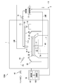
- FIG. 1 is a schematic cross-sectional view showing a substrate processing apparatus 100.
- the substrate processing apparatus 100 supplies the processing liquid LQ to the substrate W while rotating the substrate W to process the substrate W.
- the substrate processing apparatus 100 includes a chamber 1, a spin chuck 3, a spin shaft 5, a spin motor 7, a nozzle 9, a nozzle moving portion 10, a valve V1, a pipe P1, and a first unit.
- the substrate processing apparatus 100 includes a plurality of second electrodes 32.
- the power supply device 17 corresponds to an example of a “power supply unit”.
- Chamber 1 has a substantially box shape.
- the chamber 1 includes a substrate W, a spin chuck 3, a spin shaft 5, a spin motor 7, a nozzle 9, a nozzle moving portion 10, a first electrode 11, an electrode moving portion 13, a nozzle 15, a part of a pipe P2, and a plurality of guards 16.
- a part of the wiring LN1 and a part of the wiring LN2 are housed.
- the spin chuck 3 holds the substrate W and rotates. Specifically, the spin chuck 3 rotates the substrate W around the rotation axis AX of the spin chuck 3 while holding the substrate W horizontally in the chamber 1.
- the spin chuck 3 includes a plurality of chuck members 31 and a spin base 33.
- the plurality of chuck members 31 are provided on the spin base 33.
- the plurality of chuck members 31 hold the substrate W in a horizontal posture. Therefore, the chuck member 31 comes into contact with the substrate W.
- the plurality of chuck members 31 correspond to an example of the “board holding portion”.
- the spin base 33 has a substantially disk shape and supports a plurality of chuck members 31 in a horizontal posture.
- the spin shaft 5 is fixed to the spin base 33. Further, the spin shaft 5 is fixed to the drive shaft of the spin motor 7. Then, the spin motor 7 rotates the spin shaft 5 to rotate the spin base 33 around the rotation axis AX. As a result, the substrate W held by the plurality of chuck members 31 provided on the spin base 33 rotates around the rotation axis AX.
- the spin shaft 5 has a substantially cylindrical shape and has an internal space 5a.
- the nozzle 9 supplies the processing liquid LQ toward the rotating substrate W.
- the nozzle 9 corresponds to an example of a “treatment liquid supply unit”.
- the treatment liquid LQ has conductivity.
- the treatment liquid LQ contains a conductive component having a positive polarity (for example, a positive ion component) or a conductive component having a negative polarity (for example, a negative ion component).
- the positively polar conductive component is a positively charged conductive component and is a component that processes the substrate W.
- the conductive component having a negative polarity is a negatively charged conductive component and is a component that processes the substrate W.
- the conductive component having positive polarity is described as “positive conductive component”
- the conductive component having negative polarity is described as “negative conductive component”.
- the treatment liquid LQ is, for example, an etching liquid.
- each of the positive conductive component and the negative conductive component is a component that etches the substrate W.
- the etching solution as the treatment solution LQ containing a positive conductive component is, for example, hydrofluoric acid, hydrogen peroxide solution, or nitric acid.
- the etching solution as the treatment solution LQ containing a negative conductive component is, for example, ammonia, TMAH (tetramethylammonium hydroxide), or TBAH (tetrabutylammonium hydroxide).
- TMAH tetramethylammonium hydroxide
- TBAH tetrabutylammonium hydroxide
- the nozzle moving unit 10 moves the nozzle 9 between the processing position and the retracted position.
- the processing position indicates a position above the substrate W.
- the processing liquid LQ is supplied toward the substrate W.
- the retracted position indicates a position on the radial side of the substrate W with respect to the substrate W.
- the nozzle moving unit 10 includes an arm 111, a rotating shaft 113, and a nozzle moving mechanism 115.
- the arm 111 extends along a substantially horizontal direction.
- a nozzle 9 is attached to the tip of the arm 111.
- the arm 111 is coupled to the rotation shaft 113.
- the rotation shaft 113 extends along a substantially vertical direction.
- the nozzle moving mechanism 115 rotates the rotation shaft 113 around the rotation axis along the substantially vertical direction, and rotates the arm 111 along the substantially horizontal plane.
- the nozzle 9 moves along a substantially horizontal plane.
- the nozzle movement mechanism 115 includes an arm swing motor that rotates the rotation shaft 113 around the rotation axis.
- the arm swing motor is, for example, a servo motor.
- the nozzle moving mechanism 115 raises and lowers the rotation shaft 113 along a substantially vertical direction to raise and lower the arm 111. As a result, the nozzle 9 moves along the substantially vertical direction.
- the nozzle moving mechanism 115 includes a ball screw mechanism and an arm elevating motor that applies a driving force to the ball screw mechanism.
- the arm elevating motor is, for example, a servo motor.
- the pipe P1 supplies the processing liquid LQ to the nozzle 9.
- the valve V1 switches between starting and stopping the supply of the processing liquid LQ to the nozzle 9.
- the nozzle 15 supplies the rinse liquid toward the rotating substrate W after the substrate W is processed by the treatment liquid LQ.
- the rinse solution is, for example, deionized water, carbonated water, electrolytic ionized water, hydrogen water, ozone water, or hydrochloric acid water having a diluted concentration (for example, about 10 ppm to 100 ppm).
- the type of rinsing liquid is not particularly limited as long as the substrate W can be rinsed.
- the pipe P2 supplies the rinse liquid to the nozzle 15.
- the valve V2 switches between starting and stopping the supply of the rinse liquid to the nozzle 15.
- the first electrode 11 comes into contact with the treatment liquid LQ adhering to the substrate W.
- the material of the first electrode 11 is, for example, a resin material containing carbon.
- the carbon is, for example, a carbon nanotube.
- the resin is, for example, a fluororesin.
- the fluororesin is, for example, polytetrafluoroethylene (tetrafluoride) or polychlorotrifluoroethylene (trifluoride).
- the electrode moving unit 13 moves the first electrode 11 between the contact position and the retracted position.
- the contact position indicates a position where the first electrode 11 contacts the processing liquid LQ adhering to the substrate W from above the processing liquid LQ.
- the retracted position indicates a position on the radial side of the substrate W with respect to the substrate W.
- the electrode moving portion 13 includes an arm 131, a rotating shaft 133, and an electrode moving mechanism 135.
- the first electrode 11 is attached to the tip of the arm 131.
- the arm 131 is driven by the rotation shaft 133 and the electrode moving mechanism 135 to rotate along a substantially horizontal plane or move up and down along a substantially vertical direction.
- the configurations of the arm 131, the rotating shaft 133, and the electrode moving mechanism 135 are the same as the configurations of the arm 111, the rotating shaft 113, and the nozzle moving mechanism 115, respectively.
- the second electrode 32 comes into contact with the substrate W.
- the chuck member 31 functions as the second electrode 32. Therefore, according to the first embodiment, the number of parts can be reduced as compared with the case where the second electrode 32 is provided as a dedicated part.
- the material of the second electrode 32 (that is, the chuck member 31) is, for example, a resin material containing carbon. That is, the material of the second electrode 32 is the same as the material of the first electrode 11.
- At least one of the first electrode 11 and the second electrode 32 may be a resin material containing carbon. Further, the materials of the first electrode 11 and the second electrode 32 are not particularly limited as long as they have conductivity.
- the wiring LN1 connects the first electrode 11 and the power supply device 17.
- the wiring LN2 connects each of the plurality of second electrodes 32 to the power supply device 17.
- the wiring LN2 is drawn out from each of the plurality of second electrodes 32 to the power supply device 17 through the internal space 5a of the spin shaft 5.
- the wiring LN2 is connected to one second electrode 32 (that is, one chuck member 31).
- the power supply device 17 applies a DC voltage between the first electrode 11 and the second electrode 32. Therefore, according to the first embodiment, a plurality of structures constituting the pattern of the substrate W can be positively or negatively charged. As a result, it is possible to control the movement of the conductive component of the treatment liquid LQ with respect to the gaps between the plurality of structures constituting the pattern of the substrate W.
- the negative conductive component contained in the treatment liquid LQ can be guided to the gap between the plurality of structures. Therefore, the negative conductive component quickly enters the gap between the plurality of structures. As a result, a plurality of structures can be effectively treated by the negative conductive component.
- the positive conductive component contained in the treatment liquid LQ can be guided into the gap between the plurality of structures. Therefore, the positive conductive component quickly enters the gap between the plurality of structures. As a result, a plurality of structures can be effectively treated by the positive conductive component.
- the positive conductivity contained in the treatment liquid LQ is formed in the gap between the plurality of structures.
- the entry of components is suppressed. Therefore, the processing of the plurality of structures by the positive conductive component is promptly stopped. As a result, it is possible to prevent the plurality of structures from being excessively treated by the positive conductive component.
- the negative conductivity contained in the treatment liquid LQ is formed in the gap between the plurality of structures.
- the entry of components is suppressed. Therefore, the processing of the plurality of structures by the negative conductive component is promptly stopped. As a result, it is possible to prevent the plurality of structures from being excessively treated by the negative conductive component.
- the post-treatment product is, for example, a substance produced by the reaction of the treatment liquid LQ with the structure.
- the gaps After treatment the product can be effectively discharged from.
- Each of the plurality of guards 16 has a substantially tubular shape. Each of the plurality of guards 16 receives the liquid (treatment liquid LQ or rinse liquid) discharged from the substrate W.
- the guard 16 is provided according to the type of liquid discharged from the substrate W.
- the control device 19 controls each configuration of the substrate processing device 100.
- the control device 19 includes a computer. Specifically, the control device 19 includes a control unit 191 and a storage unit 193.
- the control unit 191 controls a spin chuck 3, a spin motor 7, a nozzle moving unit 10, a valve V1, an electrode moving unit 13, a valve V2, a plurality of guards 16, and a power supply device 17.
- the control unit 191 includes a processor such as a CPU (Central Processing Unit).
- the storage unit 193 includes a storage device and stores data and computer programs.
- the storage device includes a main storage device such as a semiconductor memory and an auxiliary storage device such as a semiconductor memory and / or a hard disk drive.
- the storage device may include removable media.
- the processor of the control unit 191 executes a computer program stored in the storage device of the storage unit 193, and executes a spin chuck 3, a spin motor 7, a nozzle moving unit 10, a valve V1, an electrode moving unit 13, a valve V2, and a plurality of components. Controls the guard 16 and the power supply device 17.
- the substrate processing apparatus 100 for inducing the negative conductive component into the gaps between the plurality of structures of the substrate W.
- the operation of is explained.
- the treatment liquid LQ is an etching liquid
- FIG. 2 is a diagram showing the behavior of the processing liquid LQ adhering to the substrate W in a general substrate processing apparatus.
- FIG. 2 a part of the surface of the substrate W is enlarged and shown.
- the substrate W has a substrate main body 21 and a pattern PT.
- the substrate body 21 is made of silicon.
- the pattern PT is, for example, a fine pattern.
- the pattern PT includes a plurality of structures 23.
- the structure 23 is, for example, a fine structure.
- Each of the plurality of structures 23 extends along a predetermined direction D.
- the predetermined direction D indicates a direction that intersects the surface 21a of the substrate main body 21.
- the predetermined direction D indicates a direction substantially orthogonal to the surface 21a of the substrate main body 21.
- the distance L of the structures 23 adjacent to each other is, for example, 10 nm or less.
- Each of the plurality of structures 23 is composed of a single layer or a plurality of layers.
- the structure 23 is an insulating layer, a semiconductor layer, or a conductor layer.
- the structure 23 may include an insulating layer, a semiconductor layer, a conductor layer, an insulating layer, a semiconductor layer, and a conductor layer. Two or more of them may be included.
- the insulating layer is, for example, a silicon oxide film or a silicon nitride film.
- the semiconductor layer is, for example, a polysilicon film or an amorphous silicon film.
- the conductor layer is, for example, a metal film.
- the metal film is, for example, a film containing at least one of titanium, tungsten, copper, and aluminum.
- the processing liquid LQ is supplied to the substrate W, and the processing liquid LQ is attached to the substrate W.
- the treatment liquid LQ contains a plurality of negative conductive components ECN.
- ECN negative conductive component
- the substrate processing apparatus 100 cancels the zeta potential ZP generated on each surface of the plurality of structures 23, and the polarity of each surface of the plurality of structures 23 is opposite to that of the negative conductive component ECN.
- Each surface of the plurality of structures 23 is charged so as to have a positive polarity (that is, a positive polarity). That is, the substrate processing apparatus 100 positively charges the surfaces of the plurality of structures 23. Specifically, it is as follows.
- FIG. 3 is a schematic view showing a configuration when the substrate processing apparatus 100 according to the first embodiment positively charges the surfaces of a plurality of structures 23 of the substrate W.
- the first electrode 11 is in contact with the processing liquid LQ adhering to the substrate W.
- the second electrode 32 is in contact with the substrate W.
- the negative electrode of the power supply device 17 is connected to the first electrode 11 by the wiring LN1.
- the positive electrode of the power supply device 17 is connected to the second electrode 32 by the wiring LN2.
- the power supply device 17 applies a DC voltage between the first electrode 11 and the second electrode 32. Therefore, a positive charge is supplied to the substrate W from the positive electrode of the power supply device 17.
- the zeta potential ZP FIG. 2
- FIG. 4 is a schematic view showing the behavior of the processing liquid LQ when the surfaces of the plurality of structures 23 of the substrate W are positively charged. In FIG. 4, a part of the surface of the substrate W is enlarged and shown.
- the processing liquid LQ is supplied to the substrate W, and the processing liquid LQ is attached to the substrate W.
- the treatment liquid LQ contains a plurality of negative conductive components ECN.
- the negative charges based on the zeta potential ZP shown in FIG. 2 are canceled and the surfaces of the plurality of structures 23 are positively charged. Therefore, the polarity of the surface of the structure 23 and the polarity of the negative conductive component ECN of the treatment liquid LQ are opposite to each other.
- the negative conductive component ECN is attracted to the positive charge on the surface of the structure 23 and can easily enter the gap GP between the plurality of structures 23. Therefore, the plurality of structures 23 can be effectively etched by the negative conductive component ECN.
- the structure 23, which can be negatively charged by the zeta potential, is formed of, for example, silicon, alumina in an alkaline solution, or silicon oxide.
- the surfaces of the plurality of structures 23 on the substrate W may be positively charged by the zeta potential.
- the structure 23, which can be positively charged by the zeta potential, is formed, for example, by silicon oxide, alumina, or silicon nitride in acidity.
- the treatment liquid LQ may contain a plurality of positive conductive components.
- the positive electrode of the power supply device 17 is connected to the first electrode 11 by the wiring LN1.
- the negative electrode of the power supply device 17 is connected to the second electrode 32 by the wiring LN2. Then, the power supply device 17 applies a DC voltage between the first electrode 11 and the second electrode 32. Therefore, a negative charge is supplied to the substrate W from the negative electrode of the power supply device 17. As a result, the zeta potentials on the surfaces of the plurality of structures 23 of the substrate W are canceled, and the surfaces of the plurality of structures 23 are negatively charged.
- the polarity of the surface of the structure 23 and the polarity of the positive conductive component of the treatment liquid LQ are opposite to each other.
- the positive conductive component is attracted to the negative charge on the surface of the structure 23 and can easily enter the gap GP between the plurality of structures 23. Therefore, the plurality of structures 23 can be effectively etched by the positive conductive component.
- the structure 23 of the substrate W will be further described with reference to FIG. It is preferable that the distance L between the structures 23 adjacent to each other among the plurality of structures 23 satisfies the first predetermined condition (hereinafter, referred to as “first predetermined condition PC1”).
- the first predetermined condition PC1 is a treatment liquid having the same polarity as the charge based on the zeta potential on the surface of the structure 23 before the DC voltage is applied between the first electrode 11 and the second electrode 32 by the power supply device 17. It shows that the conductive component in LQ cannot enter or penetrate the gap GP between the plurality of structures 23.
- the first electrode 11 and the second electrode 11 and the second are By applying a DC voltage between the electrode 32 and the electrode 32, the conductive component of the treatment liquid LQ can enter or permeate into the gap GP between the structures 23. As a result, the plurality of structures 23 can be effectively etched.
- the distance L between the structures 23 adjacent to each other among the plurality of structures 23 satisfies the second predetermined condition (hereinafter, referred to as “second predetermined condition PC2”).
- the second predetermined condition PC2 has a polarity opposite to the charge on the surface of the structure 23 charged by the DC voltage after the DC voltage is applied between the first electrode 11 and the second electrode 32 by the power supply device 17. It is shown that the conductive component in the treatment liquid LQ can enter or permeate the gap GP between the plurality of structures 23.
- the distance L when the distance L is 10 nm or less, the distance L satisfies the first predetermined condition PC1 and the second predetermined condition PC2.
- the application of the present invention is not limited to the case where the distance L satisfies the first predetermined condition PC1 and the second predetermined condition PC2.
- the polarity of each surface of the plurality of structures 23 of the substrate W is the polarity of the treatment liquid LQ (specifically, the treatment).
- the power supply device 17 applies a DC voltage between the first electrode 11 and the second electrode 32 so that the polarity is opposite to that of the polarity of the conductive component of the liquid LQ. Therefore, the conductive component contained in the treatment liquid LQ is attracted by the electric charge on the surface of the structure 23 of the substrate W and can easily enter the gap GP between the plurality of structures 23. As a result, the plurality of structures 23 can be effectively etched by the conductive component of the treatment liquid LQ.
- the power supply device 17 applies a DC voltage between the first electrode 11 and the second electrode 32 so as to cancel the zeta potentials on the surfaces of the plurality of structures 23. , Each surface of the plurality of structures 23 is charged. Therefore, it is possible to suppress the inhibition of etching by the treatment liquid LQ due to the zeta potentials on the surfaces of the plurality of structures 23.
- FIG. 5 is a schematic view showing a configuration when the substrate processing apparatus 100 according to the first embodiment negatively charges the surfaces of a plurality of structures 23 of the substrate W.
- the first electrode 11 is in contact with the processing liquid LQ adhering to the substrate W.
- the second electrode 32 is in contact with the substrate W.
- the positive electrode of the power supply device 17 is connected to the first electrode 11 by the wiring LN1.
- the negative electrode of the power supply device 17 is connected to the second electrode 32 by the wiring LN2.
- the power supply device 17 applies a DC voltage between the first electrode 11 and the second electrode 32. Therefore, a negative charge is supplied to the substrate W from the negative electrode of the power supply device 17.
- the surfaces of the plurality of structures 23 are negatively charged.
- FIG. 6 is a schematic view showing the behavior of the processing liquid LQ when the surfaces of the plurality of structures 23 of the substrate W are negatively charged.
- the processing liquid LQ is supplied to the substrate W, and the processing liquid LQ is attached to the substrate W.
- the treatment liquid LQ contains a plurality of negative conductive components ECN.
- the surfaces of the plurality of structures 23 are negatively charged. Therefore, the polarity of the surface of the structure 23 and the polarity of the negative conductive component ECN of the treatment liquid LQ are the same.
- the negative conductive component ECN is suppressed from entering the gap GP between the plurality of structures 23.
- the etching of the plurality of structures 23 by the negative conductive component ECN can be stopped quickly.
- the post-treatment product PD is, for example, a substance produced by the reaction of the negative conductive component ECN of the treatment liquid LQ with the structure 23.
- the treatment liquid LQ may contain a plurality of positive conductive components.
- the negative electrode of the power supply device 17 is connected to the first electrode 11 by the wiring LN1.
- the positive electrode of the power supply device 17 is connected to the second electrode 32 by the wiring LN2. Then, the power supply device 17 applies a DC voltage between the first electrode 11 and the second electrode 32. Therefore, a positive charge is supplied to the substrate W from the positive electrode of the power supply device 17. As a result, the surfaces of the plurality of structures 23 are positively charged.
- the polarity of the surface of the structure 23 and the polarity of the positive conductive component of the treatment liquid LQ are the same.
- the positive conductive component is suppressed from entering the gap GP between the plurality of structures 23.
- the etching of the plurality of structures 23 by the positive conductive component can be stopped quickly.
- the post-treatment product PD is, for example, a substance produced by the reaction between the positive conductive component of the treatment liquid LQ and the structure 23.
- the polarity of the surface of each of the plurality of structures 23 of the substrate W is the polarity of the treatment liquid LQ (specifically, the treatment).
- the power supply device 17 applies a DC voltage between the first electrode 11 and the second electrode 32 so as to have the same polarity as the polarity of the conductive component of the liquid LQ. Therefore, the conductive component contained in the treatment liquid LQ is suppressed from entering the gap GP between the plurality of structures 23 by repelling the electric charge on the surface of the structure 23. As a result, the etching of the plurality of structures 23 by the conductive component of the treatment liquid LQ can be stopped quickly. In addition, the treated product PD existing in the gaps between the plurality of structures 23 can be quickly discharged from the gap GP.
- the power supply device 17 applies a DC voltage between the first electrode 11 and the second electrode 32 so as to cancel the zeta potential on each surface of the plurality of structures 23, and each of the plurality of structures 23.
- the surface of the surface may be charged.
- the substrate processing apparatus 100 executes the substrate processing method.
- the substrate W having the pattern PT including the plurality of structures 23 is processed.
- FIG. 7 is a flowchart showing a substrate processing method. As shown in FIG. 7, the substrate processing method includes steps S1 to S15.
- step S1 the control unit 191 of the substrate processing device 100 controls the transfer robot so that the transfer robot (not shown) carries the substrate W into the substrate processing device 100. As a result, the transfer robot carries the substrate W into the substrate processing device 100.
- step S2 the control unit 191 controls the plurality of chuck members 31 so that the plurality of chuck members 31 hold the substrate W. As a result, the plurality of chuck members 31 hold the substrate W. Then, the plurality of chuck members 31 come into contact with the substrate.
- Step S2 corresponds to an example of "a step of bringing the second electrode 32 into contact with the substrate W". This is because the chuck member 31 functions as the second electrode 32.
- step S3 the control unit 191 controls the spin motor 7 so that the spin motor 7 drives the spin chuck 3 to start the rotation of the substrate W.
- the spin chuck 3 rotates and the substrate W rotates.
- step S4 the control unit 191 controls the valve V1 and the nozzle moving unit 10 so that the nozzle 9 starts supplying the processing liquid LQ toward the substrate W.
- the nozzle 9 moves to the processing position and supplies the processing liquid LQ toward the substrate W.
- the nozzle 9 supplies the processing liquid LQ to the substrate W over the first predetermined period.
- step S5 the control unit 191 controls the valve V1 and the nozzle moving unit 10 so that the nozzle 9 ends the supply of the processing liquid LQ to the substrate W.
- the nozzle 9 ends the supply of the processing liquid LQ to the substrate W and moves to the retracted position.
- step S6 the control unit 191 controls the electrode moving unit 13 so that the first electrode 11 comes into contact with the processing liquid LQ adhering to the substrate W. As a result, the first electrode 11 comes into contact with the treatment liquid LQ adhering to the substrate W.
- step S7 the control unit 191 between the first electrode 11 and the second electrode 32 so that the polarities of the plurality of structures 23 of the substrate W are opposite to the polarities of the treatment liquid LQ.
- the power supply device 17 to which a DC voltage is applied is controlled.
- the power supply device 17 has the first electrode 11 and the second electrode 32 over a second predetermined period so that the polarity of each surface of the plurality of structures 23 is opposite to the polarity of the treatment liquid LQ.
- a DC voltage is applied between them.
- the power supply device 17 stops applying the DC voltage.
- step S8 the control unit 191 switches the polarity of the power supply device 17.
- step S9 the control unit 191 transmits a direct current between the first electrode 11 and the second electrode 32 so that the polarities of the plurality of structures 23 of the substrate W are the same as the polarities of the treatment liquid LQ.
- the power supply device 17 to which the voltage is applied is controlled.
- the power supply device 17 has the first electrode 11 and the second electrode over a third predetermined period so that the polarity of each surface of the plurality of structures 23 of the substrate W becomes the same polarity as the polarity of the treatment liquid LQ.
- a DC voltage is applied between the device and the device 32. Then, the power supply device 17 stops applying the DC voltage.
- step S10 the control unit 191 controls the electrode moving unit 13 so that the first electrode 11 is separated from the processing liquid LQ adhering to the substrate W. As a result, the first electrode 11 is separated from the treatment liquid LQ and moves to the retracted position.
- step S11 the control unit 191 controls the valve V2 so that the nozzle 15 supplies the rinse liquid toward the substrate W.
- the nozzle 15 supplies the rinse liquid toward the substrate W.
- the nozzle 15 supplies the rinse liquid to the substrate W over a fourth predetermined period.
- the treatment liquid LQ on the substrate W is washed away by the rinsing liquid, and the substrate W is washed.
- step S12 the control unit 191 controls the spin motor 7 so as to accelerate the spin chuck 3 to a high rotation speed and maintain the rotation speed of the spin chuck 3 at a high rotation speed.
- the substrate W rotates at a high rotation speed, the rinse liquid adhering to the substrate W is shaken off, and the substrate W is dried.
- step S13 the control unit 191 controls the spin motor 7 so that the spin motor 7 stops the spin chuck 3 and stops the rotation of the substrate W. As a result, the spin chuck 3 stops and the substrate W stops.
- step S14 the control unit 191 controls the plurality of chuck members 31 so that the plurality of chuck members 31 release the holding of the substrate W. As a result, the plurality of chuck members 31 release the holding of the substrate W and open the substrate W.
- step S15 the control unit 191 controls the transfer robot so that the transfer robot (not shown) carries out the substrate W from the substrate processing device 100. As a result, the transfer robot carries out the substrate W from the substrate processing device 100. Then, the process ends.
- the power supply device 17 applies a DC voltage between the first electrode 11 and the second electrode 32 (step). S7 or step S9). Therefore, the plurality of structures 23 constituting the pattern PT of the substrate W can be positively or negatively charged. As a result, it is possible to control the movement of the conductive component of the processing liquid LQ with respect to the gap GP between the plurality of structures 23 constituting the pattern PT of the substrate W.
- the semiconductor substrate W having the pattern PT including the plurality of structures 23 is processed by the substrate processing method including the steps S1 to S15, and the processed semiconductor substrate W is used.
- the substrate processing method and the semiconductor manufacturing method may include at least one of the steps S7 and S9. In this case, step S8 is unnecessary. Further, the step S5 may be executed between the steps S6 and S7, may be executed between the steps S7 and S8, or may be executed between the steps S8 and S9. It may be executed between the steps S9 and S10, or it may be executed between the steps S10 and S11.
- the plurality of chuck members 31 function as the "board holding portion", but the configuration of the "board holding portion” is not particularly limited as long as the substrate W can be held.
- the substrate processing device 100 may include a vacuum chuck that functions as a “board holding unit”. The vacuum chuck holds the substrate W by vacuum suction. In this case, the vacuum chuck can function as the second electrode 32.
- the substrate processing apparatus 100 may include the second electrode 32 separately from the "substrate holding portion" such as the chuck member 31.
- FIG. 8 is a schematic cross-sectional view showing the substrate processing apparatus 100A according to the second embodiment.
- the nozzle 9 functions as the first electrode 11. Therefore, the number of parts can be reduced as compared with the case where the first electrode 11 is provided as a dedicated part.
- the material of the nozzle 9 that functions as the first electrode 11 is, for example, a resin material containing carbon. That is, the material of the nozzle 9 is the same as the material of the first electrode 11 according to the first embodiment.
- the second embodiment has the same effect as that of the first embodiment.
- the wiring LN1 connects the nozzle 9 and the power supply device 17.
- the control unit 191 controls the nozzle moving unit 10 so that the nozzle 9 functioning as the first electrode 11 comes into contact with the processing liquid LQ adhering to the substrate W. To do. As a result, the nozzle 9 functioning as the first electrode 11 comes into contact with the processing liquid LQ adhering to the substrate W.
- step S10 the control unit 191 controls the nozzle moving unit 10 so that the nozzle 9 functioning as the first electrode 11 is separated from the processing liquid LQ adhering to the substrate W. As a result, the nozzle 9 functioning as the first electrode 11 is separated from the processing liquid LQ and moves to the retracted position.
- the present invention has been described above with reference to the drawings. However, the present invention is not limited to the above-described embodiment, and can be implemented in various embodiments without departing from the gist thereof.
- the plurality of components disclosed in the above embodiment can be appropriately modified. For example, one component of all components shown in one embodiment may be added to another component of another embodiment, or some component of all components shown in one embodiment. The element may be removed from the embodiment.
- the present invention relates to a substrate processing apparatus, a substrate processing method, and a semiconductor manufacturing method, and has industrial applicability.
Landscapes
- Cleaning Or Drying Semiconductors (AREA)
- Weting (AREA)
Abstract
本発明は、基板のパターンを構成している複数の構造物の相互間の空間に対する処理液の導電成分の移動を制御できる基板処理装置、基板処理方法、および、半導体製造方法を提供することを目的とする。 本発明において、基板処理装置(100)は、複数の構造物を含むパターンを有する基板(W)を処理する。基板処理装置(100)は、処理液供給部と、第1電極(11)と、第2電極(32)と、電源部(17)とを備える。処理液供給部は、導電性を有する処理液(LQ)を基板(W)に向けて供給する。第1電極(11)は、基板(W)に付着した処理液(LQ)に接触する。第2電極(32)は、基板(W)に接触する。電源部(17)は、第1電極(11)と第2電極(32)との間に直流電圧を印加する。
Description
本発明は、基板処理装置、基板処理方法、および、半導体製造方法に関する。
特許文献1に記載されている基板処理装置は、対向部材と、複数の電源装置と、制御装置とを備える。対向部材は、基板の下面に対向する。対向部材は複数の電極を含む。複数の電極は、回転軸線からの径方向の距離が異なる複数の位置にそれぞれ配置されている。複数の電源装置は、それぞれ、複数の電極に直流電圧を印加する。制御装置は、径方向内側から径方向外側に向かって順番に印加電圧が増加するように、各電源装置に指令を与える。その結果、エッチングの均一性を高めることができる。
エッチングの均一性を高めることができる理由は、次の通りである。すなわち、基板のエッチング量は、基板の上面中央部で最も大きく、基板の上面中央部から離れるにしたがって減少する。一方、基板の上面を帯電させると、エッチングレートが増加し、さらに、エッチングレートは、基板の上面の帯電量が増加するにしたがって増加する。そこで、基板の上面中央部から離れるにしたがって連続的または段階的に帯電量が増加するように基板の上面を帯電させると、エッチングの均一性を高めることができる。
しかしながら、特許文献1に記載されている基板処理装置では、基板の径方向内側と径方向外側との間でのエッチングの均一性を高めているに過ぎない。
一方、近年、基板に形成されるパターンは、微細化されている。つまり、基板の表面において、パターンを構成している複数の微細構造物の相互間の間隙が、狭小化している。従って、エッチング液等の処理液の導電成分が複数の微細構造物の相互間の間隙に進入することが困難な場合が発生し得る。一方、一定の処理が完了すると、複数の微細構造物の相互間の間隙に、処理液の導電成分が進入することを速やかに停止したい場合が発生し得る。
本発明は上記課題に鑑みてなされたものであり、その目的は、基板のパターンを構成している複数の構造物の相互間の間隙に対する処理液の導電成分の移動を制御できる基板処理装置、基板処理方法、および、半導体製造方法を提供することにある。
本発明の一局面によれば、基板処理装置は、複数の構造物を含むパターンを有する基板を処理する。基板処理装置は、処理液供給部と、第1電極と、第2電極と、電源部とを備える。処理液供給部は、導電性を有する処理液を前記基板に向けて供給する。第1電極は、前記基板に付着した前記処理液に接触する。第2電極は、前記基板に接触する。電源部は、前記第1電極と前記第2電極との間に直流電圧を印加する。
本発明の基板処理装置において、前記複数の構造物の各々の表面の極性が、前記処理液の極性と逆の極性になるように、前記電源部は、前記第1電極と前記第2電極との間に前記直流電圧を印加することが好ましい。
本発明の基板処理装置において、前記複数の構造物の各々の表面の極性が、前記処理液の極性と同じ極性になるように、前記電源部は、前記第1電極と前記第2電極との間に前記直流電圧を印加することが好ましい。
本発明の基板処理装置において、前記複数の構造物の各々の表面のゼータ電位を打ち消すように、前記電源部は、前記第1電極と前記第2電極との間に前記直流電圧を印加して、前記複数の構造物の各々の表面を帯電させることが好ましい。
本発明の基板処理装置において、前記処理液供給部は、前記第1電極として機能することが好ましい。
本発明の基板処理装置は、前記基板を保持する基板保持部をさらに備えることが好ましい。前記基板保持部は、前記第2電極として機能することが好ましい。
本発明の基板処理装置において、前記第1電極の材料および前記第2電極の材料のうちの少なくとも一方は、炭素を含有する樹脂材料であることが好ましい。
本発明の他の局面によれば、基板処理方法において、複数の構造物を含むパターンを有する基板が処理される。基板処理方法は、導電性を有する処理液を前記基板に向けて供給する工程と、前記基板に付着した前記処理液に第1電極を接触させる工程と、前記基板に第2電極を接触させる工程と、前記第1電極と前記第2電極との間に直流電圧を印加する工程とを含む。
本発明の基板処理方法において、前記直流電圧を印加する前記工程では、前記複数の構造物の各々の表面の極性が、前記処理液の極性と逆の極性になるように、前記第1電極と前記第2電極との間に前記直流電圧を印加することが好ましい。
本発明の基板処理方法において、前記直流電圧を印加する前記工程では、前記複数の構造物の各々の表面の極性が、前記処理液の極性と同じ極性になるように、前記第1電極と前記第2電極との間に前記直流電圧を印加することが好ましい。
本発明の基板処理方法において、前記直流電圧を印加する前記工程では、前記複数の構造物の各々の表面のゼータ電位を打ち消すように、前記第1電極と前記第2電極との間に前記直流電圧を印加して、前記複数の構造物の各々の表面を帯電させることが好ましい。
本発明の基板処理方法において、前記処理液を前記基板に向けて供給する前記工程では、処理液供給部が、前記処理液を前記基板に向けて供給することが好ましい。前記第1電極を接触させる前記工程では、前記処理液供給部が、前記第1電極として機能することが好ましい。
本発明の基板処理方法において、前記第2電極を接触させる前記工程では、前記基板を保持する基板保持部が、前記第2電極として機能することが好ましい。
本発明の基板処理方法において、前記第1電極の材料および前記第2電極の材料のうちの少なくとも一方は、炭素を含有する樹脂材料であることが好ましい。
本発明のさらに他の局面によれば、半導体製造方法において、複数の構造物を含むパターンを有する半導体基板を処理して、処理後の前記半導体基板である半導体が製造される。半導体製造方法は、導電性を有する処理液を前記半導体基板に向けて供給する工程と、前記半導体基板に付着した前記処理液に第1電極を接触させる工程と、前記半導体基板に第2電極を接触させる工程と、前記第1電極と前記第2電極との間に直流電圧を印加する工程とを含む。
本発明によれば、基板のパターンを構成している複数の構造物の相互間の空間に対する処理液の導電成分の移動を制御できる基板処理装置、基板処理方法、および、半導体製造方法を提供できる。
以下、本発明の実施形態について、図面を参照しながら説明する。なお、図中、同一または相当部分については同一の参照符号を付して説明を繰り返さない。また、本発明の実施形態において、X軸、Y軸、及びZ軸は互いに直交し、X軸及びY軸は水平方向に平行であり、Z軸は鉛直方向に平行である。なお、図面の簡略化のため、断面を示す斜線を適宜省略する。
(実施形態1)
図1~図7を参照して、本発明の実施形態1に係る基板処理装置100を説明する。基板処理装置100は処理液によって基板Wを処理する。以下、処理液を「処理液LQ」と記載する。基板Wは、例えば、半導体ウエハ、液晶表示装置用基板、プラズマディスプレイ用基板、電界放出ディスプレイ(Field Emission Display:FED)用基板、光ディスク用基板、磁気ディスク用基板、光磁気ディスク用基板、フォトマスク用基板、セラミック基板、又は、太陽電池用基板である。基板Wは、例えば、略円板状である。以下の実施形態1の説明では、基板Wは半導体基板である。
図1~図7を参照して、本発明の実施形態1に係る基板処理装置100を説明する。基板処理装置100は処理液によって基板Wを処理する。以下、処理液を「処理液LQ」と記載する。基板Wは、例えば、半導体ウエハ、液晶表示装置用基板、プラズマディスプレイ用基板、電界放出ディスプレイ(Field Emission Display:FED)用基板、光ディスク用基板、磁気ディスク用基板、光磁気ディスク用基板、フォトマスク用基板、セラミック基板、又は、太陽電池用基板である。基板Wは、例えば、略円板状である。以下の実施形態1の説明では、基板Wは半導体基板である。
まず、図1を参照して基板処理装置100を説明する。図1は、基板処理装置100を示す模式的断面図である。図1に示すように、基板処理装置100は、基板Wを回転しながら、基板Wに処理液LQを供給して、基板Wを処理する。具体的には、基板処理装置100は、チャンバー1と、スピンチャック3と、スピン軸5と、スピンモーター7と、ノズル9と、ノズル移動部10と、バルブV1と、配管P1と、第1電極11と、電極移動部13と、ノズル15と、バルブV2と、配管P2と、複数のガード16と、電源装置17と、制御装置19と、配線LN1と、配線LN2と、少なくとも1つの第2電極32とを備える。実施形態1では、基板処理装置100は、複数の第2電極32を備える。電源装置17は、「電源部」の一例に相当する。
チャンバー1は略箱形状を有する。チャンバー1は、基板W、スピンチャック3、スピン軸5、スピンモーター7、ノズル9、ノズル移動部10、第1電極11、電極移動部13、ノズル15、配管P2の一部、複数のガード16、配線LN1の一部、および、配線LN2の一部を収容する。
スピンチャック3は、基板Wを保持して回転する。具体的には、スピンチャック3は、チャンバー1内で基板Wを水平に保持しながら、スピンチャック3の回転軸線AXの回りに基板Wを回転させる。
スピンチャック3は、複数のチャック部材31と、スピンベース33とを含む。複数のチャック部材31はスピンベース33に設けられる。複数のチャック部材31は基板Wを水平な姿勢で保持する。従って、チャック部材31は基板Wに接触する。複数のチャック部材31は、「基板保持部」の一例に相当する。スピンベース33は、略円板状であり、水平な姿勢で複数のチャック部材31を支持する。
スピン軸5は、スピンベース33に固定される。また、スピン軸5は、スピンモーター7の駆動軸に固定される。そして、スピンモーター7は、スピン軸5を回転させることによって、スピンベース33を回転軸線AXの回りに回転させる。その結果、スピンベース33に設けられた複数のチャック部材31に保持された基板Wが回転軸線AXの回りに回転する。スピン軸5は、略円筒形状を有し、内部空間5aを有する。
ノズル9は、回転中の基板Wに向けて処理液LQを供給する。ノズル9は、「処理液供給部」の一例に相当する。
処理液LQは導電性を有する。処理液LQは、プラス極性を有する導電成分(例えばプラスイオン成分)、または、マイナス極性を有する導電成分(例えばマイナスイオン成分)を含む。プラス極性を有する導電成分は、プラスに帯電した導電成分であって、基板Wを処理する成分である。マイナス極性を有する導電成分は、マイナスに帯電した導電成分であって、基板Wを処理する成分である。
以下の説明では、プラス極性を有する導電成分を「プラス導電成分」と記載し、マイナス極性を有する導電成分を「マイナス導電成分」と記載する。また、「プラス導電成分」と「マイナス導電成分」とを区別して説明する必要のないときは、「プラス導電成分」と「マイナス導電成分」とを総称して、「導電成分」と記載する場合がある。
処理液LQは、例えば、エッチング液である。処理液LQがエッチング液である場合、プラス導電成分およびマイナス導電成分の各々は、基板Wをエッチングする成分である。
プラス導電成分を含む処理液LQとしてのエッチング液は、例えば、フッ酸、過酸化水素水、または、硝酸である。マイナス導電成分を含む処理液LQとしてのエッチング液は、例えば、アンモニア、TMAH(テトラメチルアンモニウムハイドロオキサイド)、または、TBAH(テトラブチルアンモニウムハイドロオキサイド)である。なお、処理液LQが導電性を有する限りは、処理液LQの種類は、特に限定されない。
ノズル移動部10は、処理位置と退避位置との間でノズル9を移動する。処理位置は、基板Wの上方の位置を示す。ノズル9は、処理位置に位置するときに、基板Wに向けて処理液LQを供給する。退避位置は、基板Wよりも基板Wの径方向外側の位置を示す。
具体的には、ノズル移動部10は、アーム111と、回動軸113と、ノズル移動機構115とを含む。アーム111は略水平方向に沿って延びる。アーム111の先端部にはノズル9が取り付けられる。アーム111は回動軸113に結合される。回動軸113は、略鉛直方向に沿って延びる。ノズル移動機構115は、回動軸113を略鉛直方向に沿った回動軸線のまわりに回動させて、アーム111を略水平面に沿って回動させる。その結果、ノズル9が略水平面に沿って移動する。例えば、ノズル移動機構115は、回動軸113を回動軸線のまわりに回動させるアーム揺動モーターを含む。アーム揺動モーターは、例えば、サーボモータである。また、ノズル移動機構115は、回動軸113を略鉛直方向に沿って昇降させて、アーム111を昇降させる。その結果、ノズル9が略鉛直方向に沿って移動する。例えば、ノズル移動機構115は、ボールねじ機構と、ボールねじ機構に駆動力を与えるアーム昇降モーターとを含む。アーム昇降モーターは、例えば、サーボモータである。
配管P1はノズル9に処理液LQを供給する。バルブV1は、ノズル9に対する処理液LQの供給開始と供給停止とを切り替える。
ノズル15は、処理液LQによって基板Wが処理された時よりも後に、回転中の基板Wに向けてリンス液を供給する。リンス液は、例えば、脱イオン水、炭酸水、電解イオン水、水素水、オゾン水、または、希釈濃度(例えば、10ppm~100ppm程度)の塩酸水である。リンス液の種類は、基板Wをリンスできる限りにおいては、特に限定されない。
配管P2はノズル15にリンス液を供給する。バルブV2は、ノズル15に対するリンス液の供給開始と供給停止とを切り替える。
第1電極11は、基板Wに付着した処理液LQに接触する。第1電極11の材料は、例えば、炭素を含有する樹脂材料である。炭素は、例えば、カーボンナノチューブである。樹脂は、例えば、フッ素樹脂である。フッ素樹脂は、例えば、ポリテトラフルオロエチレン(4フッ化)、または、ポリクロロトリフルオロエチレン(3フッ化)である。このように第1電極11を構成することで、実施形態1では、第1電極11の導電性を確保しつつ耐薬性を向上できる。
電極移動部13は、接触位置と退避位置との間で第1電極11を移動する。接触位置は、基板Wに付着した処理液LQに対して、第1電極11が処理液LQの上方から接触する位置を示す。退避位置は、基板Wよりも基板Wの径方向外側の位置を示す。具体的には、電極移動部13は、アーム131と、回動軸133と、電極移動機構135とを含む。アーム131の先端部には第1電極11が取り付けられる。アーム131は、回動軸133および電極移動機構135によって駆動されて、略水平面に沿って回動され、または、略鉛直方向に沿って昇降される。その他、アーム131、回動軸133、および電極移動機構135の構成は、それぞれ、アーム111、回動軸113、およびノズル移動機構115の構成と同様である。
第2電極32は基板Wに接触する。実施形態1では、チャック部材31が第2電極32として機能する。従って、実施形態1によれば、第2電極32を専用部品として設ける場合と比較して、部品点数を削減できる。第2電極32(つまり、チャック部材31)の材料は、例えば、炭素を含む樹脂材料である。つまり、第2電極32の材料は、第1電極11の材料と同様である。このように第2電極32を構成することで、実施形態1では、第2電極32の導電性を確保しつつ耐薬性を向上できる。
なお、例えば、第1電極11および第2電極32のうちの少なくとも一方が、炭素を含む樹脂材料であってもよい。また、第1電極11および第2電極32の材料は、導電性を有する限りにおいては特に限定されない。
配線LN1は、第1電極11と電源装置17とを接続する。配線LN2は、複数の第2電極32の各々と電源装置17とを接続する。配線LN2は、スピン軸5の内部空間5aを通って、複数の第2電極32の各々から電源装置17まで引き出されている。なお、基板処理装置100が、1つの第2電極32を有している場合は、配線LN2は、1つの第2電極32(つまり、1つのチャック部材31)に接続される。
電源装置17は、第1電極11と第2電極32との間に直流電圧を印加する。従って、実施形態1によれば、基板Wのパターンを構成している複数の構造物をプラスまたはマイナスに帯電させることができる。その結果、基板Wのパターンを構成している複数の構造物の相互間の間隙に対する処理液LQの導電成分の移動を制御できる。
例えば、基板Wのパターンを構成している複数の構造物がプラスに帯電されると、処理液LQに含まれるマイナス導電成分を、複数の構造物の相互間の間隙に誘導できる。従って、マイナス導電成分が、速やかに複数の構造物の相互間の間隙に進入する。その結果、マイナス導電成分によって、複数の構造物を効果的に処理できる。
例えば、基板Wのパターンを構成している複数の構造物がマイナスに帯電されると、処理液LQに含まれるプラス導電成分を、複数の構造物の相互間の間隙に誘導できる。従って、プラス導電成分が、速やかに複数の構造物の相互間の間隙に進入する。その結果、プラス導電成分によって、複数の構造物を効果的に処理できる。
例えば、一定の処理の完了後において、基板Wのパターンを構成している複数の構造物がプラスに帯電されると、複数の構造物の相互間の間隙に、処理液LQに含まれるプラス導電成分が進入することが抑制される。従って、プラス導電成分による複数の構造物の処理が速やかに停止される。その結果、プラス導電成分によって、複数の構造物が過剰に処理されることを抑制できる。
例えば、一定の処理の完了後において、基板Wのパターンを構成している複数の構造物がマイナスに帯電されると、複数の構造物の相互間の間隙に、処理液LQに含まれるマイナス導電成分が進入することが抑制される。従って、マイナス導電成分による複数の構造物の処理が速やかに停止される。その結果、マイナス導電成分によって、複数の構造物が過剰に処理されることを抑制できる。
例えば、複数の構造物の相互間の間隙に存在する処理後生成物がプラスに帯電している場合に、基板Wのパターンを構成している複数の構造物がプラスに帯電されると、間隙から処理後生成物を効果的に排出できる。処理後生成物は、例えば、処理液LQと構造物との反応によって生成された物質である。
例えば、複数の構造物の相互間の間隙に存在する処理後生成物がマイナスに帯電している場合に、基板Wのパターンを構成している複数の構造物がマイナスに帯電されると、間隙から処理後生成物を効果的に排出できる。
複数のガード16の各々は略筒形状を有する。複数のガード16の各々は、基板Wから排出された液体(処理液LQまたはリンス液)を受け止める。なお、ガード16は、基板Wから排出される液体の種類に応じて設けられる。
制御装置19は、基板処理装置100の各構成を制御する。制御装置19はコンピューターを含む。具体的には、制御装置19は、制御部191と、記憶部193とを含む。制御部191は、スピンチャック3、スピンモーター7、ノズル移動部10、バルブV1、電極移動部13、バルブV2、複数のガード16、および、電源装置17を制御する。制御部191は、CPU(Central Processing Unit)のようなプロセッサーを含む。記憶部193は、記憶装置を含み、データ及びコンピュータープログラムを記憶する。記憶装置は、半導体メモリーのような主記憶装置と、半導体メモリー及び/又はハードディスクドライブのような補助記憶装置とを含む。記憶装置は、リムーバブルメディアを含んでいてもよい。制御部191のプロセッサーは、記憶部193の記憶装置が記憶しているコンピュータープログラムを実行して、スピンチャック3、スピンモーター7、ノズル移動部10、バルブV1、電極移動部13、バルブV2、複数のガード16、および、電源装置17を制御する。
次に、図2~図4を参照して、処理液LQがマイナス導電成分を含む場合において、基板Wの複数の構造物の相互間の間隙にマイナス導電成分を誘導するときの基板処理装置100の動作を説明する。図2~図4の説明では、処理液LQがエッチング液である例を説明する。
まず、図2を参照して、処理液LQの一般的な挙動を説明する。図2は、一般的な基板処理装置において基板Wに付着した処理液LQの挙動を示す図である。図2では、基板Wの表面の一部が拡大して示されている。
図2に示すように、基板Wは、基板本体21と、パターンPTとを有する。基板本体21は、シリコンによって形成される。パターンPTは、例えば、微細パターンである。パターンPTは、複数の構造物23を含む。構造物23は、例えば、微細構造物である。
複数の構造物23の各々は、所定方向Dに沿って延びている。所定方向Dは、基板本体21の表面21aに対して交差する方向を示す。実施形態1では、所定方向Dは、基板本体21の表面21aに対して略直交する方向を示す。互いに隣り合う構造物23の距離Lは、例えば、10nm以下である。
複数の構造物23の各々は、単層または複数層によって構成される。構造物23が単層によって構成される場合、構造物23は、絶縁層、半導体層、または、導体層である。構造物23が複数層によって構成される場合、構造物23は、絶縁層を含んでもよいし、半導体層を含んでもよいし、導体層を含んでもよいし、絶縁層と半導体層と導体層とのうちの2以上を含んでもよい。
絶縁層は、例えば、シリコン酸化膜またはシリコン窒化膜である。半導体層は、例えば、ポリシリコン膜、または、アモルファスシリコン膜である。導体層は、例えば、金属膜である。金属膜は、例えば、チタン、タングステン、銅、および、アルミニウムのうちの少なくとも1つを含む膜である。
図2では、基板Wに処理液LQが供給されて、基板Wには処理液LQが付着している。処理液LQは、複数のマイナス導電成分ECNを含む。一方、複数の構造物23の各々の表面にはゼータ電位ZPが発生するため、複数の構造物23の各々の表面は、ゼータ電位ZPによってマイナスに帯電している。従って、構造物23の極性とマイナス導電成分ECNの極性とは同じである。その結果、マイナス導電成分ECNは、構造物23に対して反発し、複数の構造物23の相互間の間隙GPに進入することが困難である。
そこで、実施形態1では、基板処理装置100は、複数の構造物23の各々の表面に発生したゼータ電位ZPを打ち消して、複数の構造物23の各々の表面の極性がマイナス導電成分ECNと逆の極性(つまり、プラスの極性)になるように、複数の構造物23の各々の表面を帯電させる。つまり、基板処理装置100は、複数の構造物23の各々の表面をプラスに帯電させる。具体的には、次の通りである。
図3は、実施形態1に係る基板処理装置100が基板Wの複数の構造物23の表面をプラスに帯電させるときの構成を示す模式図である。図3に示すように、第1電極11は、基板Wに付着した処理液LQに接触している。一方、第2電極32は基板Wに接触している。そして、電源装置17のマイナス極が、配線LN1によって第1電極11に接続される。一方、電源装置17のプラス極が、配線LN2によって第2電極32に接続される。そして、電源装置17は、第1電極11と第2電極32との間に直流電圧を印加する。従って、電源装置17のプラス極から、基板Wに正電荷が供給される。その結果、基板Wの複数の構造物23の表面のゼータ電位ZP(図2)が打ち消されて、複数の構造物23の表面がプラスに帯電する。
図4は、基板Wの複数の構造物23の表面をプラスに帯電させたときの処理液LQの挙動を示す模式図である。図4では、基板Wの表面の一部が拡大して示されている。
図4に示すように、基板Wに処理液LQが供給されて、基板Wには処理液LQが付着している。処理液LQは、複数のマイナス導電成分ECNを含む。一方、複数の構造物23では、図2に示すゼータ電位ZPに基づくマイナスの電荷が打ち消されて、複数の構造物23の表面がプラスに帯電している。従って、構造物23の表面の極性と処理液LQのマイナス導電成分ECNの極性とは逆である。その結果、マイナス導電成分ECNは、構造物23の表面のプラス電荷に引き付けられて、複数の構造物23の相互間の間隙GPに容易に進入することができる。よって、マイナス導電成分ECNによって、複数の構造物23を効果的にエッチングできる。
なお、ゼータ電位によってマイナスに帯電し得る構造物23は、例えば、シリコン、アルカリ溶液中のアルミナ、または、シリコン酸化物によって形成される。
一方、基板Wの複数の構造物23の各々の表面が、ゼータ電位によってプラスに帯電する場合がある。ゼータ電位によってプラスに帯電し得る構造物23は、例えば、酸性中のシリコン酸化物、アルミナ、または、シリコンナイトライドによって形成される。そして、処理液LQが、複数のプラス導電成分を含む場合がある。
この場合は、電源装置17のプラス極が、配線LN1によって第1電極11に接続される。一方、電源装置17のマイナス極が、配線LN2によって第2電極32に接続される。そして、電源装置17は、第1電極11と第2電極32との間に直流電圧を印加する。従って、電源装置17のマイナス極から、基板Wに負電荷が供給される。その結果、基板Wの複数の構造物23の表面のゼータ電位が打ち消されて、複数の構造物23の表面がマイナスに帯電する。
複数の構造物23の表面がマイナスに帯電すると、構造物23の表面の極性と処理液LQのプラス導電成分の極性とは逆である。その結果、プラス導電成分は、構造物23の表面のマイナス電荷に引き付けられて、複数の構造物23の相互間の間隙GPに容易に進入することができる。よって、プラス導電成分によって、複数の構造物23を効果的にエッチングできる。
引き続き図4を参照して、基板Wの構造物23をさらに説明する。複数の構造物23のうち互いに隣り合う構造物23の間の距離Lは、第1所定条件(以下、「第1所定条件PC1」と記載する。)を満たすことが好ましい。第1所定条件PC1は、電源装置17によって第1電極11と第2電極32との間に直流電圧が印加される前では、構造物23の表面のゼータ電位に基づく電荷と同極性の処理液LQ中の導電成分が、複数の構造物23の相互間の間隙GPに進入または浸透できないことを示す。実施形態1によれば、複数の構造物23が、第1所定条件PC1を満たすような狭小な距離Lを有する複数の超微細構造物である場合であっても、第1電極11と第2電極32との間に直流電圧を印加することで、処理液LQの導電成分を構造物23の相互間の間隙GPに進入または浸透させることができる。その結果、複数の構造物23を効果的にエッチングできる。
換言すれば、複数の構造物23のうち互いに隣り合う構造物23の間の距離Lは、第2所定条件(以下、「第2所定条件PC2」と記載する。)を満たすことが好ましい。第2所定条件PC2は、電源装置17によって第1電極11と第2電極32との間に直流電圧が印加された後では、直流電圧によって帯電された構造物23の表面の電荷と逆極性の処理液LQ中の導電成分が、複数の構造物23の相互間の間隙GPに進入または浸透できることを示す。
なお、例えば、距離Lが10nm以下であると、距離Lは第1所定条件PC1および第2所定条件PC2を満たす。ただし、本発明の適用は、距離Lが第1所定条件PC1および第2所定条件PC2を満たす場合に限定されない。
以上、図3および図4を参照して説明したように、実施形態1によれば、基板Wの複数の構造物23の各々の表面の極性が、処理液LQの極性(具体的には処理液LQの導電成分の極性)と逆の極性になるように、電源装置17は、第1電極11と第2電極32との間に直流電圧を印加する。従って、処理液LQに含まれる導電成分は、基板Wの構造物23の表面の電荷に引き付けられて、複数の構造物23の相互間の間隙GPに容易に進入することができる。その結果、処理液LQの導電成分によって、複数の構造物23を効果的にエッチングできる。
また、実施形態1によれば、複数の構造物23の各々の表面のゼータ電位を打ち消すように、電源装置17は、第1電極11と第2電極32との間に直流電圧を印加して、複数の構造物23の各々の表面を帯電させる。従って、複数の構造物23の表面のゼータ電位に起因して処理液LQによるエッチングが阻害されることを抑制できる。
次に、図5および図6を参照して、処理液LQがマイナス導電成分を含む場合において、基板Wの複数の構造物23の相互間の間隙GPへのマイナス導電成分の進入を抑制するときの基板処理装置100の動作を説明する。図5および図6の説明では、処理液LQがエッチング液である例を説明する。
図5は、実施形態1に係る基板処理装置100が基板Wの複数の構造物23の表面をマイナスに帯電させるときの構成を示す模式図である。図5に示すように、第1電極11は、基板Wに付着した処理液LQに接触している。一方、第2電極32は基板Wに接触している。そして、電源装置17のプラス極が、配線LN1によって第1電極11に接続される。一方、電源装置17のマイナス極が、配線LN2によって第2電極32に接続される。そして、電源装置17は、第1電極11と第2電極32との間に直流電圧を印加する。従って、電源装置17のマイナス極から、基板Wに負電荷が供給される。その結果、複数の構造物23の表面がマイナスに帯電する。
図6は、基板Wの複数の構造物23の表面をマイナスに帯電させたときの処理液LQの挙動を示す模式図である。図6に示すように、基板Wに処理液LQが供給されて、基板Wには処理液LQが付着している。処理液LQは、複数のマイナス導電成分ECNを含む。一方、複数の構造物23の表面がマイナスに帯電している。従って、構造物23の表面の極性と処理液LQのマイナス導電成分ECNの極性とは同じである。その結果、複数の構造物23の相互間の間隙GPに、マイナス導電成分ECNが進入することが抑制される。その結果、マイナス導電成分ECNによる複数の構造物23のエッチングを速やかに停止できる。
また、複数の構造物23の相互間の間隙GPに存在する処理後生成物PDがマイナスに帯電していると、処理後生成物PDは、複数の構造物23の表面のマイナス電荷によって間隙GPから押し出される。その結果、処理後生成物PDを間隙GPから速やかに排出できる。処理後生成物PDは、例えば、処理液LQのマイナス導電成分ECNと構造物23との反応によって生成された物質である。
一方、処理液LQが、複数のプラス導電成分を含む場合がある。この場合は、電源装置17のマイナス極が、配線LN1によって第1電極11に接続される。一方、電源装置17のプラス極が、配線LN2によって第2電極32に接続される。そして、電源装置17は、第1電極11と第2電極32との間に直流電圧を印加する。従って、電源装置17のプラス極から、基板Wに正電荷が供給される。その結果、複数の構造物23の表面がプラスに帯電する。
複数の構造物23の表面がプラスに帯電すると、構造物23の表面の極性と処理液LQのプラス導電成分の極性とは同じである。その結果、複数の構造物23の相互間の間隙GPに、プラス導電成分が進入することが抑制される。その結果、プラス導電成分による複数の構造物23のエッチングを速やかに停止できる。
また、複数の構造物23の相互間の間隙GPに存在する処理後生成物PDがプラスに帯電していると、処理後生成物PDは、複数の構造物23の表面のプラス電荷によって間隙GPから押し出される。その結果、処理後生成物PDを間隙GPから速やかに排出できる。処理後生成物PDは、例えば、処理液LQのプラス導電成分と構造物23との反応によって生成された物質である。
以上、図5および図6を参照して説明したように、実施形態1によれば、基板Wの複数の構造物23の各々の表面の極性が、処理液LQの極性(具体的には処理液LQの導電成分の極性)と同じ極性になるように、電源装置17は、第1電極11と第2電極32との間に直流電圧を印加する。従って、処理液LQに含まれる導電成分は、構造物23の表面の電荷に反発して、複数の構造物23の相互間の間隙GPに進入することが抑制される。その結果、処理液LQの導電成分による複数の構造物23のエッチングを速やかに停止できる。また、複数の構造物23の間隙に存在する処理後生成物PDを間隙GPから速やかに排出できる。
なお、基板Wの複数の構造物23の各々の表面の極性が、処理液LQの極性と同じ極性になるように第1電極11と第2電極32との間に直流電圧を印加する場合に、複数の構造物23の各々の表面のゼータ電位を打ち消すように、電源装置17は、第1電極11と第2電極32との間に直流電圧を印加して、複数の構造物23の各々の表面を帯電させてもよい。
次に、図1および図7を参照して、本発明の実施形態1に係る基板処理方法を説明する。基板処理装置100が基板処理方法を実行する。基板処理方法においては、複数の構造物23を含むパターンPTを有する基板Wが処理される。図7は、基板処理方法を示すフローチャートである。図7に示すように、基板処理方法は、工程S1~工程S15を含む。
図1および図7に示すように、工程S1において、基板処理装置100の制御部191は、搬送ロボット(不図示)が基板処理装置100に基板Wを搬入するように、搬送ロボットを制御する。その結果、搬送ロボットが基板処理装置100に基板Wを搬入する。
次に、工程S2において、制御部191は、複数のチャック部材31が基板Wを保持するように、複数のチャック部材31を制御する。その結果、複数のチャック部材31が基板Wを保持する。そして、複数のチャック部材31が基板に接触する。工程S2は、「基板Wに第2電極32を接触させる工程」の一例に相当する。チャック部材31が第2電極32として機能するからである。
次に、工程S3において、制御部191は、スピンモーター7がスピンチャック3を駆動して基板Wの回転を開始するように、スピンモーター7を制御する。その結果、スピンチャック3が回転して、基板Wが回転する。
次に、工程S4において、制御部191は、ノズル9が基板Wに向けて処理液LQの供給を開始するように、バルブV1およびノズル移動部10を制御する。その結果、ノズル9は、処理位置に移動して基板Wに向けて処理液LQを供給する。具体的には、ノズル9は、第1所定期間にわたって基板Wに処理液LQを供給する。
次に、工程S5において、制御部191は、ノズル9が基板Wに対する処理液LQの供給を終了するように、バルブV1およびノズル移動部10を制御する。その結果、ノズル9は、基板Wへの処理液LQの供給を終了して退避位置に移動する。
次に、工程S6において、制御部191は、第1電極11が基板Wに付着した処理液LQに接触するように、電極移動部13を制御する。その結果、第1電極11が基板Wに付着した処理液LQに接触する。
次に、工程S7において、制御部191は、基板Wの複数の構造物23の極性が処理液LQの極性と逆の極性になるように、第1電極11と第2電極32との間に直流電圧を印加する電源装置17を制御する。その結果、電源装置17は、複数の構造物23の各々の表面の極性が処理液LQの極性と逆の極性になるように、第2所定期間にわたって第1電極11と第2電極32との間に直流電圧を印加する。そして、電源装置17は、直流電圧の印加を停止する。
次に、工程S8において、制御部191は、電源装置17の極性を切り替える。
次に、工程S9において、制御部191は、基板Wの複数の構造物23の極性が処理液LQの極性と同じ極性になるように、第1電極11と第2電極32との間に直流電圧を印加する電源装置17を制御する。その結果、電源装置17は、基板Wの複数の構造物23の各々の表面の極性が、処理液LQの極性と同じ極性になるように、第3所定期間にわたって第1電極11と第2電極32との間に直流電圧を印加する。そして、電源装置17は、直流電圧の印加を停止する。
次に、工程S10において、制御部191は、第1電極11が基板Wに付着した処理液LQから離隔するように、電極移動部13を制御する。その結果、第1電極11は、処理液LQから離隔して、退避位置に移動する。
次に、工程S11において、制御部191は、ノズル15が基板Wに向けてリンス液を供給するように、バルブV2を制御する。その結果、ノズル15は、基板Wに向けてリンス液を供給する。具体的には、ノズル15は、第4所定期間にわたって基板Wにリンス液を供給する。その結果、基板W上の処理液LQがリンス液によって洗い流されて、基板Wが洗浄される。
次に、工程S12において、制御部191は、スピンチャック3を高回転速度まで加速させてスピンチャック3の回転速度を高回転速度に維持するように、スピンモーター7を制御する。その結果、基板Wが高回転速度で回転して、基板Wに付着しているリンス液が振り切られて基板Wが乾燥される。
次に、工程S13において、制御部191は、スピンモーター7がスピンチャック3を停止して基板Wの回転を停止するように、スピンモーター7を制御する。その結果、スピンチャック3が停止して、基板Wが停止する。
次に、工程S14において、制御部191は、複数のチャック部材31が基板Wの保持を解除するように、複数のチャック部材31を制御する。その結果、複数のチャック部材31が、基板Wの保持を解除して、基板Wを開放する。
次に、工程S15において、制御部191は、搬送ロボット(不図示)が基板処理装置100から基板Wを搬出するように、搬送ロボットを制御する。その結果、搬送ロボットが基板処理装置100から基板Wを搬出する。そして、処理が終了する。
以上、図7を参照して説明したように、実施形態1に係る基板処理方法によれば、電源装置17は、第1電極11と第2電極32との間に直流電圧を印加する(工程S7または工程S9)。従って、基板WのパターンPTを構成している複数の構造物23をプラスまたはマイナスに帯電させることができる。その結果、基板WのパターンPTを構成している複数の構造物23の相互間の間隙GPに対する処理液LQの導電成分の移動を制御できる。
また、実施形態1に係る半導体製造方法では、複数の構造物23を含むパターンPTを有する半導体基板Wを、工程S1~工程S15を含む基板処理方法によって処理して、処理後の半導体基板Wである半導体を製造する。
なお、基板処理方法および半導体製造方法は、工程S7と工程S9とのうちの少なくとも一方を含んでいればよい。この場合は、工程S8は不要である。また、工程S5は、工程S6と工程S7との間に実行されてもよいし、工程S7と工程S8との間に実行されてもよいし、工程S8と工程S9との間に実行されてもよいし、工程S9と工程S10との間に実行されてもよいし、工程S10と工程S11との間に実行されてもよい。
また、実施形態1では、複数のチャック部材31が「基板保持部」として機能したが、「基板保持部」の構成は、基板Wを保持できる限りにおいては、特に限定されない。例えば、基板処理装置100は、「基板保持部」として機能するバキュームチャックを備えていてもよい。バキュームチャックは、真空吸着により基板Wを保持する。この場合は、バキュームチャックが第2電極32として機能することが可能である。
なお、基板処理装置100は、第2電極32を、チャック部材31等の「基板保持部」と別個に備えていてもよい。
(実施形態2)
図8を参照して、本発明の実施形態2に係る基板処理装置100Aを説明する。実施形態2では、ノズル9が第1電極11として機能する点で、実施形態2は実施形態1と主に異なる。以下、実施形態2が実施形態1と異なる点を主に説明する。
図8を参照して、本発明の実施形態2に係る基板処理装置100Aを説明する。実施形態2では、ノズル9が第1電極11として機能する点で、実施形態2は実施形態1と主に異なる。以下、実施形態2が実施形態1と異なる点を主に説明する。
図8は、実施形態2に係る基板処理装置100Aを示す模式的断面図である。図8に示すように、基板処理装置100Aにおいては、ノズル9が第1電極11として機能する。従って、第1電極11を専用部品として設ける場合と比較して、部品点数を削減できる。第1電極11として機能するノズル9の材料は、例えば、炭素を含む樹脂材料である。つまり、ノズル9の材料は、実施形態1に係る第1電極11の材料と同様である。このようにノズル9を構成することで、第1電極11として機能するノズル9の導電性を確保しつつ耐薬性を向上できる。その他、実施形態2では、実施形態1と同様の効果を有する。また、配線LN1は、ノズル9と電源装置17とを接続する。
なお、実施形態2では、図7に示す工程S6において、制御部191は、第1電極11として機能するノズル9が基板Wに付着した処理液LQに接触するように、ノズル移動部10を制御する。その結果、第1電極11として機能するノズル9が基板Wに付着した処理液LQに接触する。
また、工程S10において、制御部191は、第1電極11として機能するノズル9が基板Wに付着した処理液LQから離隔するように、ノズル移動部10を制御する。その結果、第1電極11として機能するノズル9は、処理液LQから離隔して、退避位置に移動する。
以上、図面を参照して本発明の実施形態について説明した。ただし、本発明は、上記の実施形態に限られるものではなく、その要旨を逸脱しない範囲で種々の態様において実施できる。また、上記の実施形態に開示される複数の構成要素は適宜改変可能である。例えば、ある実施形態に示される全構成要素のうちのある構成要素を別の実施形態の構成要素に追加してもよく、または、ある実施形態に示される全構成要素のうちのいくつかの構成要素を実施形態から削除してもよい。
また、図面は、発明の理解を容易にするために、それぞれの構成要素を主体に模式的に示しており、図示された各構成要素の厚さ、長さ、個数、間隔等は、図面作成の都合上から実際とは異なる場合もある。また、上記の実施形態で示す各構成要素の構成は一例であって、特に限定されるものではなく、本発明の効果から実質的に逸脱しない範囲で種々の変更が可能であることは言うまでもない。
本発明は、基板処理装置、基板処理方法、および、半導体製造方法に関するものであり、産業上の利用可能性を有する。
9 ノズル(処理液供給部)
11 第1電極
17 電源装置(電源部)
31 チャック部材(基板保持部)
32 第2電極
100、100A 基板処理装置
W 基板
11 第1電極
17 電源装置(電源部)
31 チャック部材(基板保持部)
32 第2電極
100、100A 基板処理装置
W 基板
Claims (15)
- 複数の構造物を含むパターンを有する基板を処理する基板処理装置であって、
導電性を有する処理液を前記基板に向けて供給する処理液供給部と、
前記基板に付着した前記処理液に接触する第1電極と、
前記基板に接触する第2電極と、
前記第1電極と前記第2電極との間に直流電圧を印加する電源部と
を備える、基板処理装置。 - 前記複数の構造物の各々の表面の極性が、前記処理液の極性と逆の極性になるように、前記電源部は、前記第1電極と前記第2電極との間に前記直流電圧を印加する、請求項1に記載の基板処理装置。
- 前記複数の構造物の各々の表面の極性が、前記処理液の極性と同じ極性になるように、前記電源部は、前記第1電極と前記第2電極との間に前記直流電圧を印加する、請求項1に記載の基板処理装置。
- 前記複数の構造物の各々の表面のゼータ電位を打ち消すように、前記電源部は、前記第1電極と前記第2電極との間に前記直流電圧を印加して、前記複数の構造物の各々の表面を帯電させる、請求項1から請求項3のいずれか1項に記載の基板処理装置。
- 前記処理液供給部は、前記第1電極として機能する、請求項1から請求項4のいずれか1項に記載の基板処理装置。
- 前記基板を保持する基板保持部をさらに備え、
前記基板保持部は、前記第2電極として機能する、請求項1から請求項5のいずれか1項に記載の基板処理装置。 - 前記第1電極の材料および前記第2電極の材料のうちの少なくとも一方は、炭素を含有する樹脂材料である、請求項1から請求項6のいずれか1項に記載の基板処理装置。
- 複数の構造物を含むパターンを有する基板を処理する基板処理方法であって、
導電性を有する処理液を前記基板に向けて供給する工程と、
前記基板に付着した前記処理液に第1電極を接触させる工程と、
前記基板に第2電極を接触させる工程と、
前記第1電極と前記第2電極との間に直流電圧を印加する工程と
を含む、基板処理方法。 - 前記直流電圧を印加する前記工程では、前記複数の構造物の各々の表面の極性が、前記処理液の極性と逆の極性になるように、前記第1電極と前記第2電極との間に前記直流電圧を印加する、請求項8に記載の基板処理方法。
- 前記直流電圧を印加する前記工程では、前記複数の構造物の各々の表面の極性が、前記処理液の極性と同じ極性になるように、前記第1電極と前記第2電極との間に前記直流電圧を印加する、請求項8に記載の基板処理方法。
- 前記直流電圧を印加する前記工程では、前記複数の構造物の各々の表面のゼータ電位を打ち消すように、前記第1電極と前記第2電極との間に前記直流電圧を印加して、前記複数の構造物の各々の表面を帯電させる、請求項8から請求項10のいずれか1項に記載の基板処理方法。
- 前記処理液を前記基板に向けて供給する前記工程では、処理液供給部が、前記処理液を前記基板に向けて供給し、
前記第1電極を接触させる前記工程では、前記処理液供給部が、前記第1電極として機能する、請求項8から請求項11のいずれか1項に記載の基板処理方法。 - 前記第2電極を接触させる前記工程では、前記基板を保持する基板保持部が、前記第2電極として機能する、請求項8から請求項12のいずれか1項に記載の基板処理方法。
- 前記第1電極の材料および前記第2電極の材料のうちの少なくとも一方は、炭素を含有する樹脂材料である、請求項8から請求項13のいずれか1項に記載の基板処理方法。
- 複数の構造物を含むパターンを有する半導体基板を処理して、処理後の前記半導体基板である半導体を製造する半導体製造方法であって、
導電性を有する処理液を前記半導体基板に向けて供給する工程と、
前記半導体基板に付着した前記処理液に第1電極を接触させる工程と、
前記半導体基板に第2電極を接触させる工程と、
前記第1電極と前記第2電極との間に直流電圧を印加する工程と
を含む、半導体製造方法。
Applications Claiming Priority (2)
| Application Number | Priority Date | Filing Date | Title |
|---|---|---|---|
| JP2019053335A JP2020155614A (ja) | 2019-03-20 | 2019-03-20 | 基板処理装置、基板処理方法、および、半導体製造方法 |
| JP2019-053335 | 2019-03-20 |
Publications (1)
| Publication Number | Publication Date |
|---|---|
| WO2020189004A1 true WO2020189004A1 (ja) | 2020-09-24 |
Family
ID=72520637
Family Applications (1)
| Application Number | Title | Priority Date | Filing Date |
|---|---|---|---|
| PCT/JP2020/002326 Ceased WO2020189004A1 (ja) | 2019-03-20 | 2020-01-23 | 基板処理装置、基板処理方法、および、半導体製造方法 |
Country Status (3)
| Country | Link |
|---|---|
| JP (1) | JP2020155614A (ja) |
| TW (1) | TW202036701A (ja) |
| WO (1) | WO2020189004A1 (ja) |
Families Citing this family (2)
| Publication number | Priority date | Publication date | Assignee | Title |
|---|---|---|---|---|
| KR102863410B1 (ko) * | 2020-12-21 | 2025-09-24 | 세메스 주식회사 | 기판 지지 부재, 이를 포함하는 기판 처리 장치 및 방법 |
| WO2025187708A1 (ja) * | 2024-03-08 | 2025-09-12 | 株式会社Screenホールディングス | 基板処理方法および基板処理装置 |
Citations (7)
| Publication number | Priority date | Publication date | Assignee | Title |
|---|---|---|---|---|
| JPH01160016A (ja) * | 1987-12-16 | 1989-06-22 | Fujitsu Ltd | フォトマスクの製造方法 |
| US6010964A (en) * | 1997-08-20 | 2000-01-04 | Micron Technology, Inc. | Wafer surface treatment methods and systems using electrocapillarity |
| JP2001160545A (ja) * | 1999-12-02 | 2001-06-12 | Okamoto Machine Tool Works Ltd | 半導体基板上の白金層の化学機械研磨方法 |
| JP2002075926A (ja) * | 2000-08-30 | 2002-03-15 | Nippon Shokubai Co Ltd | 金属膜の研磨方法およびその研磨装置 |
| JP2002093761A (ja) * | 2000-09-19 | 2002-03-29 | Sony Corp | 研磨方法、研磨装置、メッキ方法およびメッキ装置 |
| WO2004075278A1 (ja) * | 2003-02-21 | 2004-09-02 | Matsushita Electric Industrial Co., Ltd. | 液相エッチング方法および液相エッチング装置 |
| WO2011101936A1 (ja) * | 2010-02-18 | 2011-08-25 | シャープ株式会社 | エッチング方法及びエッチング装置 |
-
2019
- 2019-03-20 JP JP2019053335A patent/JP2020155614A/ja active Pending
-
2020
- 2020-01-23 WO PCT/JP2020/002326 patent/WO2020189004A1/ja not_active Ceased
- 2020-02-10 TW TW109104061A patent/TW202036701A/zh unknown
Patent Citations (7)
| Publication number | Priority date | Publication date | Assignee | Title |
|---|---|---|---|---|
| JPH01160016A (ja) * | 1987-12-16 | 1989-06-22 | Fujitsu Ltd | フォトマスクの製造方法 |
| US6010964A (en) * | 1997-08-20 | 2000-01-04 | Micron Technology, Inc. | Wafer surface treatment methods and systems using electrocapillarity |
| JP2001160545A (ja) * | 1999-12-02 | 2001-06-12 | Okamoto Machine Tool Works Ltd | 半導体基板上の白金層の化学機械研磨方法 |
| JP2002075926A (ja) * | 2000-08-30 | 2002-03-15 | Nippon Shokubai Co Ltd | 金属膜の研磨方法およびその研磨装置 |
| JP2002093761A (ja) * | 2000-09-19 | 2002-03-29 | Sony Corp | 研磨方法、研磨装置、メッキ方法およびメッキ装置 |
| WO2004075278A1 (ja) * | 2003-02-21 | 2004-09-02 | Matsushita Electric Industrial Co., Ltd. | 液相エッチング方法および液相エッチング装置 |
| WO2011101936A1 (ja) * | 2010-02-18 | 2011-08-25 | シャープ株式会社 | エッチング方法及びエッチング装置 |
Also Published As
| Publication number | Publication date |
|---|---|
| TW202036701A (zh) | 2020-10-01 |
| JP2020155614A (ja) | 2020-09-24 |
Similar Documents
| Publication | Publication Date | Title |
|---|---|---|
| CN107408503B (zh) | 基板处理装置和基板处理方法 | |
| JP7233294B2 (ja) | 基板処理方法、半導体製造方法、および、基板処理装置 | |
| US9165798B2 (en) | Substrate processing apparatus and substrate processing method | |
| EP1908531A1 (en) | Apparatus for removing foreign material from substrate and method for removing foreign material from substrate | |
| TWI702312B (zh) | 半導體裝置之製造裝置及製造方法 | |
| CN109564859B (zh) | 基板处理方法以及基板处理装置 | |
| KR102301802B1 (ko) | 기판 처리 방법 및 기판 처리 장치 | |
| WO2018193920A1 (ja) | 基板処理方法および基板処理装置 | |
| JP2020155614A (ja) | 基板処理装置、基板処理方法、および、半導体製造方法 | |
| JP2009238862A (ja) | 基板処理方法および基板処理装置 | |
| KR102638633B1 (ko) | 기판 처리 방법, 반도체 제조 방법, 및, 기판 처리 장치 | |
| JP7427475B2 (ja) | 基板処理方法 | |
| CN113366615A (zh) | 基板处理方法及基板处理装置 | |
| WO2023176052A1 (ja) | 基板処理方法および基板処理装置 | |
| TW202249057A (zh) | 電漿產生裝置及基板處理裝置 | |
| JP7488729B2 (ja) | 大気圧プラズマ源、および、基板処理装置 | |
| TWI807413B (zh) | 基板處理方法 | |
| WO2025084159A1 (ja) | 基板処理装置 | |
| JP2025137415A (ja) | 基板処理方法および基板処理装置 | |
| WO2025187708A1 (ja) | 基板処理方法および基板処理装置 | |
| WO2025084158A1 (ja) | 基板処理装置 | |
| WO2025084160A1 (ja) | 基板処理装置 | |
| TW202505662A (zh) | 基板處理裝置 | |
| KR20170065790A (ko) | 반도체장치 제조용 확산장비 및 그 장비를 이용한 반도체장치 제조방법 |
Legal Events
| Date | Code | Title | Description |
|---|---|---|---|
| 121 | Ep: the epo has been informed by wipo that ep was designated in this application |
Ref document number: 20774186 Country of ref document: EP Kind code of ref document: A1 |
|
| NENP | Non-entry into the national phase |
Ref country code: DE |
|
| 122 | Ep: pct application non-entry in european phase |
Ref document number: 20774186 Country of ref document: EP Kind code of ref document: A1 |