WO2020184584A1 - 回路接続用接着剤フィルム及びその製造方法、回路接続構造体の製造方法、並びに、接着剤フィルム収容セット - Google Patents
回路接続用接着剤フィルム及びその製造方法、回路接続構造体の製造方法、並びに、接着剤フィルム収容セット Download PDFInfo
- Publication number
- WO2020184584A1 WO2020184584A1 PCT/JP2020/010387 JP2020010387W WO2020184584A1 WO 2020184584 A1 WO2020184584 A1 WO 2020184584A1 JP 2020010387 W JP2020010387 W JP 2020010387W WO 2020184584 A1 WO2020184584 A1 WO 2020184584A1
- Authority
- WO
- WIPO (PCT)
- Prior art keywords
- adhesive layer
- adhesive film
- circuit connection
- circuit
- conductive particles
- Prior art date
- Legal status (The legal status is an assumption and is not a legal conclusion. Google has not performed a legal analysis and makes no representation as to the accuracy of the status listed.)
- Ceased
Links
Images


Classifications
-
- C—CHEMISTRY; METALLURGY
- C09—DYES; PAINTS; POLISHES; NATURAL RESINS; ADHESIVES; COMPOSITIONS NOT OTHERWISE PROVIDED FOR; APPLICATIONS OF MATERIALS NOT OTHERWISE PROVIDED FOR
- C09J—ADHESIVES; NON-MECHANICAL ASPECTS OF ADHESIVE PROCESSES IN GENERAL; ADHESIVE PROCESSES NOT PROVIDED FOR ELSEWHERE; USE OF MATERIALS AS ADHESIVES
- C09J9/00—Adhesives characterised by their physical nature or the effects produced, e.g. glue sticks
- C09J9/02—Electrically-conducting adhesives
-
- C—CHEMISTRY; METALLURGY
- C09—DYES; PAINTS; POLISHES; NATURAL RESINS; ADHESIVES; COMPOSITIONS NOT OTHERWISE PROVIDED FOR; APPLICATIONS OF MATERIALS NOT OTHERWISE PROVIDED FOR
- C09J—ADHESIVES; NON-MECHANICAL ASPECTS OF ADHESIVE PROCESSES IN GENERAL; ADHESIVE PROCESSES NOT PROVIDED FOR ELSEWHERE; USE OF MATERIALS AS ADHESIVES
- C09J201/00—Adhesives based on unspecified macromolecular compounds
-
- C—CHEMISTRY; METALLURGY
- C09—DYES; PAINTS; POLISHES; NATURAL RESINS; ADHESIVES; COMPOSITIONS NOT OTHERWISE PROVIDED FOR; APPLICATIONS OF MATERIALS NOT OTHERWISE PROVIDED FOR
- C09J—ADHESIVES; NON-MECHANICAL ASPECTS OF ADHESIVE PROCESSES IN GENERAL; ADHESIVE PROCESSES NOT PROVIDED FOR ELSEWHERE; USE OF MATERIALS AS ADHESIVES
- C09J4/00—Adhesives based on organic non-macromolecular compounds having at least one polymerisable carbon-to-carbon unsaturated bond ; adhesives, based on monomers of macromolecular compounds of groups C09J183/00 - C09J183/16
-
- C—CHEMISTRY; METALLURGY
- C09—DYES; PAINTS; POLISHES; NATURAL RESINS; ADHESIVES; COMPOSITIONS NOT OTHERWISE PROVIDED FOR; APPLICATIONS OF MATERIALS NOT OTHERWISE PROVIDED FOR
- C09J—ADHESIVES; NON-MECHANICAL ASPECTS OF ADHESIVE PROCESSES IN GENERAL; ADHESIVE PROCESSES NOT PROVIDED FOR ELSEWHERE; USE OF MATERIALS AS ADHESIVES
- C09J7/00—Adhesives in the form of films or foils
- C09J7/30—Adhesives in the form of films or foils characterised by the adhesive composition
-
- H—ELECTRICITY
- H01—ELECTRIC ELEMENTS
- H01B—CABLES; CONDUCTORS; INSULATORS; SELECTION OF MATERIALS FOR THEIR CONDUCTIVE, INSULATING OR DIELECTRIC PROPERTIES
- H01B1/00—Conductors or conductive bodies characterised by the conductive materials; Selection of materials as conductors
- H01B1/20—Conductive material dispersed in non-conductive organic material
- H01B1/22—Conductive material dispersed in non-conductive organic material the conductive material comprising metals or alloys
-
- H—ELECTRICITY
- H01—ELECTRIC ELEMENTS
- H01B—CABLES; CONDUCTORS; INSULATORS; SELECTION OF MATERIALS FOR THEIR CONDUCTIVE, INSULATING OR DIELECTRIC PROPERTIES
- H01B13/00—Apparatus or processes specially adapted for manufacturing conductors or cables
-
- H—ELECTRICITY
- H01—ELECTRIC ELEMENTS
- H01B—CABLES; CONDUCTORS; INSULATORS; SELECTION OF MATERIALS FOR THEIR CONDUCTIVE, INSULATING OR DIELECTRIC PROPERTIES
- H01B5/00—Non-insulated conductors or conductive bodies characterised by their form
- H01B5/16—Non-insulated conductors or conductive bodies characterised by their form comprising conductive material in insulating or poorly conductive material, e.g. conductive rubber
-
- H—ELECTRICITY
- H01—ELECTRIC ELEMENTS
- H01R—ELECTRICALLY-CONDUCTIVE CONNECTIONS; STRUCTURAL ASSOCIATIONS OF A PLURALITY OF MUTUALLY-INSULATED ELECTRICAL CONNECTING ELEMENTS; COUPLING DEVICES; CURRENT COLLECTORS
- H01R11/00—Individual connecting elements providing two or more spaced connecting locations for conductive members which are, or may be, thereby interconnected, e.g. end pieces for wires or cables supported by the wire or cable and having means for facilitating electrical connection to some other wire, terminal, or conductive member, blocks of binding posts
- H01R11/01—Individual connecting elements providing two or more spaced connecting locations for conductive members which are, or may be, thereby interconnected, e.g. end pieces for wires or cables supported by the wire or cable and having means for facilitating electrical connection to some other wire, terminal, or conductive member, blocks of binding posts characterised by the form or arrangement of the conductive interconnection between the connecting locations
-
- H—ELECTRICITY
- H01—ELECTRIC ELEMENTS
- H01R—ELECTRICALLY-CONDUCTIVE CONNECTIONS; STRUCTURAL ASSOCIATIONS OF A PLURALITY OF MUTUALLY-INSULATED ELECTRICAL CONNECTING ELEMENTS; COUPLING DEVICES; CURRENT COLLECTORS
- H01R43/00—Apparatus or processes specially adapted for manufacturing, assembling, maintaining, or repairing of line connectors or current collectors or for joining electric conductors
-
- C—CHEMISTRY; METALLURGY
- C09—DYES; PAINTS; POLISHES; NATURAL RESINS; ADHESIVES; COMPOSITIONS NOT OTHERWISE PROVIDED FOR; APPLICATIONS OF MATERIALS NOT OTHERWISE PROVIDED FOR
- C09J—ADHESIVES; NON-MECHANICAL ASPECTS OF ADHESIVE PROCESSES IN GENERAL; ADHESIVE PROCESSES NOT PROVIDED FOR ELSEWHERE; USE OF MATERIALS AS ADHESIVES
- C09J2203/00—Applications of adhesives in processes or use of adhesives in the form of films or foils
- C09J2203/326—Applications of adhesives in processes or use of adhesives in the form of films or foils for bonding electronic components such as wafers, chips or semiconductors
-
- C—CHEMISTRY; METALLURGY
- C09—DYES; PAINTS; POLISHES; NATURAL RESINS; ADHESIVES; COMPOSITIONS NOT OTHERWISE PROVIDED FOR; APPLICATIONS OF MATERIALS NOT OTHERWISE PROVIDED FOR
- C09J—ADHESIVES; NON-MECHANICAL ASPECTS OF ADHESIVE PROCESSES IN GENERAL; ADHESIVE PROCESSES NOT PROVIDED FOR ELSEWHERE; USE OF MATERIALS AS ADHESIVES
- C09J2301/00—Additional features of adhesives in the form of films or foils
- C09J2301/40—Additional features of adhesives in the form of films or foils characterized by the presence of essential components
- C09J2301/416—Additional features of adhesives in the form of films or foils characterized by the presence of essential components use of irradiation
Definitions
- the present invention relates to an adhesive film for circuit connection and a method for manufacturing the same, a method for manufacturing a circuit connection structure, and an adhesive film accommodating set.
- An adhesive film for circuit connection having an anisotropic conductivity in which is dispersed is used.
- Patent Document 1 proposes a method in which conductive particles are unevenly distributed on one side of an anisotropic conductive adhesive sheet to separate the conductive particles from each other.
- the adhesive film for circuit connection is peeled off from the circuit member even when the circuit connection structure is used for a long period of time in a high temperature and high humidity environment (for example, 85 ° C., 85% RH) after the circuit member is connected. It is required not to.
- a high temperature and high humidity environment for example, 85 ° C., 85% RH
- the present invention uses a circuit member and an adhesive film, which are generated when the circuit connection structure is used in a high temperature and high humidity environment, while suppressing the flow of conductive particles generated during the manufacture of the circuit connection structure.
- An adhesive film for circuit connection and a method for manufacturing the same which can suppress peeling at the interface between the formed circuit connection portion, a method for manufacturing a circuit connection structure using the adhesive film, and an adhesive provided with the adhesive film. It is an object of the present invention to provide an agent film containing set.
- the circuit connecting adhesive film on one side of the present invention comprises a first adhesive layer and a second adhesive layer laminated on the first adhesive layer, and the first adhesive.
- the layer is composed of a cured product of a photocurable composition
- the second adhesive layer is composed of a thermosetting composition
- the photocurable composition is composed of a polymerizable compound and a photopolymerization initiator having an oxime ester structure.
- the content of the photopolymerization initiator is 0.3 to 1.2% by mass based on the total amount of the components other than the conductive particles in the photocurable composition.
- the connection resistance between the opposing electrodes of the circuit connection structure can be reduced, and further, even in a high temperature and high humidity environment (for example, 85 ° C., 85% RH). Low connection resistance can be maintained. That is, according to this circuit connection adhesive film, the connection reliability of the circuit connection structure can be improved.
- the method for producing an adhesive film for circuit connection on one aspect of the present invention includes a preparation step of preparing a first adhesive layer and a second adhesive composed of a thermosetting composition on the first adhesive layer.
- the preparation step includes a laminating step of laminating the layers, and the preparation step is a step of curing the photocurable composition by irradiating the layer made of the photocurable composition with light to obtain a first adhesive layer.
- the photocurable composition contains a polymerizable compound, a photopolymerization initiator having an oxime ester structure, and conductive particles, and the content of the photopolymerization initiator in the photocurable composition is It is 0.3 to 1.2% by mass based on the total amount of components other than the conductive particles.
- the interface between the circuit member and the adhesive film which is generated when the circuit connection structure is used in a high temperature and high humidity environment, while suppressing the flow of conductive particles generated during the manufacture of the circuit connection structure. It is possible to obtain an adhesive film for circuit connection that can suppress peeling in.
- the polymerizable compound may be a radically polymerizable compound having a radically polymerizable group.
- thermosetting composition may contain a radically polymerizable compound having a radically polymerizable group.
- the photopolymerization initiator having an oxime ester structure may be a compound having a structure represented by the following formula (VI).
- R 11 , R 12 and R 13 each independently represent an organic group containing a hydrogen atom, an alkyl group having 1 to 20 carbon atoms, or an aromatic hydrocarbon group.
- the thickness of the first adhesive layer may be 0.1 to 0.8 times the average particle size of the conductive particles.
- the above-mentioned circuit connection bonding is performed between the first circuit member having the first electrode and the second circuit member having the second electrode.
- a step of electrically connecting the first electrode and the second electrode to each other by heat-pressing the first circuit member and the second circuit member with an agent film interposed therebetween.
- the adhesive film accommodating set on one side of the present invention includes the above-mentioned adhesive film for circuit connection and an accommodating member accommodating the adhesive film, and the accommodating member can visually recognize the inside of the accommodating member from the outside. It has a visible portion, and the transmittance of light having a wavelength of 365 nm in the visible portion is 10% or less.
- the environment in which the adhesive film for circuit connection is used is a room called a clean room where the temperature, humidity, and cleanliness of the room are controlled at a certain level, and when shipped from the production site, it is directly exposed to the outside air.
- the circuit connection adhesive film is housed in a housing member such as a packing bag so as not to be exposed and cause quality deterioration due to dust and moisture.
- this accommodating member is made of a transparent material so that various information such as the product name, lot number, and expiration date attached to the internal adhesive film can be confirmed from outside the accommodating member. A part is provided.
- thermosetting composition when the above-mentioned adhesive film for circuit connection is housed in a conventional housing member and used after being stored or transported, the above-mentioned effects of the adhesive film may not be obtained. Revealed by. As a result of further studies by the present inventors based on such study results, when a compound capable of reacting with the photopolymerization initiator in the photocurable composition is used as the polymerizable compound in the thermosetting composition. It has been clarified that the thermosetting composition is cured during storage and transportation of the adhesive film, and the effect of reducing the connection resistance is reduced.
- the present inventors further investigated based on the speculation that the polymerization of the polymerizable compound in the thermosetting composition is proceeding by the radicals derived from the photopolymerization initiator remaining in the first adhesive layer.
- the present inventors further investigated based on the speculation that the polymerization of the polymerizable compound in the thermosetting composition is proceeding by the radicals derived from the photopolymerization initiator remaining in the first adhesive layer.
- an adhesive film accommodating set provided with the above-mentioned specific accommodating member, it is possible to suppress curing of the thermosetting composition during storage or transportation, and reduce the connection resistance of the adhesive film. We found that the effect could be maintained.
- thermosetting composition when a compound capable of reacting with the photopolymerization initiator in the photocurable composition is used as the polymerizable compound in the thermosetting composition, adhesion is performed. Curing of the thermosetting composition during storage or transportation of the agent film can be suppressed, and the effect of reducing the connection resistance of the adhesive film can be maintained.
- FIG. 1 is a schematic cross-sectional view showing an adhesive film for circuit connection according to an embodiment of the present invention.
- FIG. 2 is a schematic cross-sectional view showing a circuit connection structure according to an embodiment of the present invention.
- FIG. 3 is a schematic cross-sectional view showing a manufacturing process of the circuit connection structure according to the embodiment of the present invention.
- FIG. 4 is a perspective view showing an adhesive film accommodating set according to an embodiment of the present invention.
- FIG. 1 is a schematic cross-sectional view showing an adhesive film for circuit connection according to an embodiment.
- the circuit connection adhesive film 1 (hereinafter, also simply referred to as “adhesive film 1”) is laminated on the first adhesive layer 2 and the first adhesive layer 2.
- a second adhesive layer 3 is provided.
- the first adhesive layer 2 is made of a cured product (photo-cured product) of a photocurable composition.
- the photocurable composition is a (A) polymerizable compound (hereinafter, also referred to as “(A) component”) and (B) a photopolymerization initiator having an oxime ester structure (hereinafter, also referred to as “(B) component”). ) And (C) conductive particles 4 (hereinafter, also referred to as “component (C)”).
- the photocurable composition includes (D) a thermosetting resin (hereinafter, also referred to as “(D) component”) and / or (E) a thermal polymerization initiator (hereinafter, also referred to as “(E) component”). May be further contained. That is, the photocurable composition may be a light and thermosetting composition.
- the first adhesive layer 2 is obtained, for example, by irradiating a layer made of a photocurable composition with light energy to polymerize the component (A) and curing the photocurable composition. That is, the first adhesive layer 2 is composed of the conductive particles 4 and the adhesive component 5 obtained by photocuring the photocurable composition.
- the adhesive component 5 contains at least a polymer of the component (A).
- the adhesive component 5 may or may not contain the unreacted components (A) and (B).
- Component (A) Polymerizable compound
- the component (A) is, for example, a compound polymerized by radicals, cations or anions generated by a photopolymerization initiator by irradiation with light (for example, ultraviolet light).
- the component (A) may be any of a monomer, an oligomer or a polymer.
- the component (A) has at least one polymerizable group.
- the polymerizable group is preferably a radically polymerizable group that reacts with radicals from the viewpoint of further improving the effect of reducing the connection resistance and improving the connection reliability. That is, the component (A) is preferably a radically polymerizable compound.
- the radically polymerizable group include a vinyl group, an allyl group, a styryl group, an alkenyl group, an alkenylene group, a (meth) acryloyl group, a maleimide group and the like.
- the number of polymerizable groups contained in the component (A) may be 2 or more from the viewpoint that the physical properties required for reducing the connection resistance and the crosslink density can be easily obtained after the polymerization, and the curing shrinkage during the polymerization is suppressed. From the viewpoint, it may be 10 or less. From these viewpoints, the number of polymerizable groups contained in the component (A) may be 2 to 10. Suppressing the curing shrinkage during polymerization is preferable in that a uniform and stable film (first adhesive layer) can be obtained after light irradiation.
- a polymerizable compound having a number of polymerizable groups within the above range is used, and then a polymerizable compound having a number of polymerizable groups outside the above range is used. May be used additionally.
- component (A) examples include (meth) acrylate compound, maleimide compound, vinyl ether compound, allyl compound, styrene derivative, acrylamide derivative, nadiimide derivative, natural rubber, isoprene rubber, butyl rubber, nitrile rubber, butadiene rubber, and styrene-.
- examples thereof include butadiene rubber, acrylonitrile-butadiene rubber, and carboxylated nitrile rubber.
- Examples of the (meth) acrylate compound include epoxy (meth) acrylate, (poly) urethane (meth) acrylate, methyl (meth) acrylate, polyether (meth) acrylate, polyester (meth) acrylate, polybutadiene (meth) acrylate, and silicone acrylate.
- Maleimide compounds include 1-methyl-2,4-bismaleimidebenzene, N, N'-m-phenylene bismaleimide, N, N'-p-phenylene bismaleimide, N, N'-m-toluylene bismaleimide.
- N, N'-4,4-biphenylene bismaleimide N, N'-4,4- (3,3'-dimethyl-biphenylene) bismaleimide, N, N'-4,4- (3,3' -Dimethyldiphenylmethane) bismaleimide, N, N'-4,4- (3,3'-diethyldiphenylmethane) bismaleimide, N, N'-4,4-diphenylmethane bismaleimide, N, N'-4,4- Diphenylpropane bismaleimide, N, N'-4,4-diphenyl ether bismaleimide, N, N'-3,3-diphenylsulfone bismaleimide, 2,2-bis (4- (4-maleimidephenoxy) phenyl) propane, 2,2-bis (3-s-butyl-4-8 (4-maleimidephenoxy) phenyl) propane, 1,1-bis (4- (4-maleimidephenoxy) phenyl) de
- vinyl ether compound examples include diethylene glycol divinyl ether, dipropylene glycol divinyl ether, cyclohexanedimethanol divinyl ether, and trimethylolpropane trivinyl ether.
- allyl compound examples include 1,3-diallyl phthalate, 1,2-diallyl phthalate, and triallyl isocyanurate.
- the component (A) is preferably a (meth) acrylate compound from the viewpoint of excellent balance between the curing reaction rate and the physical properties after curing.
- the component (A) is a (poly) urethane (meth) acrylate compound from the viewpoint of achieving both cohesive force for reducing connection resistance and elongation for improving adhesive force and obtaining better adhesive properties. You can.
- the component (A) may be a (meth) acrylate compound having a high Tg skeleton such as a dicyclopentadiene skeleton from the viewpoint of improving the cohesive force and further reducing the connection resistance.
- the component (A) is the terminal or side of a thermoplastic resin such as an acrylic resin, a phenoxy resin, or a polyurethane resin from the viewpoint of balancing the crosslink density and the curing shrinkage, further reducing the connection resistance, and improving the connection reliability.
- a thermoplastic resin such as an acrylic resin, a phenoxy resin, or a polyurethane resin from the viewpoint of balancing the crosslink density and the curing shrinkage, further reducing the connection resistance, and improving the connection reliability.
- It may be a compound (for example, polyurethane (meth) acrylate) in which a polymerizable group such as a vinyl group, an allyl group, or a (meth) acryloyl group is introduced into the chain.
- the weight average molecular weight of the component (A) may be 3000 or more, 5000 or more, or 10,000 or more from the viewpoint of excellent balance between the crosslink density and the curing shrinkage.
- the weight average molecular weight of the component (A) may be 1 million or less, 500,000 or less, or 250,000 or less from the viewpoint of excellent compatibility with other components. From these viewpoints, the weight average molecular weight of the component (A) may be 30 to 1,000,000, 5,000 to 500,000, or 10,000 to 250,000.
- the weight average molecular weight refers to a value measured from a gel permeation chromatograph (GPC) using a calibration curve using standard polystyrene according to the conditions described in Examples.
- the component (A) preferably contains, as the (meth) acrylate compound, a radically polymerizable compound having a phosphoric acid ester structure represented by the following formula (1).
- the adhesive strength to the surface of the inorganic substance (metal or the like) is improved, it is suitable for adhesion between electrodes (for example, circuit electrodes).
- n represents an integer of 1 to 3
- R represents a hydrogen atom or a methyl group.
- the radically polymerizable compound having the above phosphoric acid ester structure can be obtained, for example, by reacting anhydrous phosphoric acid with 2-hydroxyethyl (meth) acrylate.
- Specific examples of the radically polymerizable compound having a phosphoric acid ester structure include mono (2- (meth) acryloyloxyethyl) acid phosphate, di (2- (meth) acryloyloxyethyl) acid phosphate and the like.
- the content of the component (A) is the total amount of the components other than the conductive particles in the photocurable composition from the viewpoint that the crosslink density required for reducing the connection resistance and improving the connection reliability can be easily obtained. As a reference, it may be 5% by mass or more, 10% by mass or more, and 20% by mass or more.
- the content of the component (A) may be 90% by mass or less, and may be 80% by mass, based on the total amount of the components other than the conductive particles in the photocurable composition from the viewpoint of suppressing curing shrinkage during polymerization. It may be less than or equal to 70% by mass or less. From these viewpoints, the content of the component (A) may be 5 to 90% by mass, and 10 to 80% by mass, based on the total amount of the components other than the conductive particles in the photocurable composition. It may be 20 to 70% by mass.
- the photocurable composition contains a photopolymerization initiator having an oxime ester structure as the component (B).
- the photopolymerization initiator may have a plurality of photopolymerization initiators having an oxime ester structure.
- the component (B) one kind of compound may be used alone, or a plurality of kinds of compounds may be used in combination.
- a compound having a structure represented by the following formula (VI) is preferably used.
- R 11 , R 12 and R 13 each independently represent an organic group containing a hydrogen atom, an alkyl group having 1 to 20 carbon atoms, or an aromatic hydrocarbon group.
- the compound having an oxime ester structure examples include 1-phenyl-1,2-butandion-2- (o-methoxycarbonyl) oxime and 1-phenyl-1,2-propanedione-2- (o-methoxycarbonyl).
- Oxime 1-phenyl-1,2-propanedione-2- (o-ethoxycarbonyl) oxime, 1-phenyl-1,2-propanedione-2-o-benzoyloxime, 1,3-diphenylpropanthrion- 2- (o-ethoxycarbonyl) oxime, 1-phenyl-3-ethoxypropanetrione-2- (o-benzoyl) oxime, 1,2-octanedione, 1- [4- (phenylthio) phenyl-, 2-( o-benzoyloxime)], etanone, 1- [9-ethyl-6- (2-methylbenzoyl) -9H-carbazole-3-yl]-, 1- (o-acetyloxime) and the like.
- the content of the photopolymerization initiator having an oxime ester structure is 0.3 mass by mass based on the total amount of components other than the conductive particles in the photocurable composition from the viewpoint of further improving the flow suppressing effect of the conductive particles. % Or more, preferably 0.45% by mass or more, more preferably 0.55% by mass or more, still more preferably 0.85% by mass or more.
- the content of the photopolymerization initiator having an oxime ester structure is 1.2% by mass or less based on the total amount of components other than the conductive particles in the photocurable composition from the viewpoint of further improving the effect of suppressing peeling. It is preferably 0.9% by mass or less, and more preferably 0.6% by mass or less.
- the content of the photopolymerization initiator having an oxime ester structure is 0.3 to 1.2% by mass based on the total amount of the components other than the conductive particles in the photocurable composition. It is preferably 0.45 to 0.9% by mass, and more preferably 0.45 to 0.6% by mass.
- the photocurable composition has an ⁇ -aminoalkylphenone structure, an aminobenzophenone structure, an N-phenylglycine structure, an acylphosphine oxide structure, a benzyl dimethyl ketal structure, and an ⁇ -.
- a photopolymerization initiator having a structure such as a hydroxyalkylphenone structure may be further contained.
- the total content of the photopolymerization initiator is 0.3% by mass or more based on the total amount of the components other than the conductive particles in the photocurable composition from the viewpoint of further improving the flow suppressing effect of the conductive particles. Yes, preferably 0.45% by mass or more, more preferably 0.55% by mass or more, still more preferably 0.85% by mass or more.
- the content of the component (B) is preferably 1.2% by mass or less based on the total amount of the components other than the conductive particles in the photocurable composition from the viewpoint of further improving the effect of suppressing peeling. It is more preferably 0.9% by mass or less, and further preferably 0.6% by mass or less.
- the content of the component (B) is preferably 0.3 to 1.2% by mass, more preferably, based on the total amount of the components other than the conductive particles in the photocurable composition. It is 0.45 to 0.9% by mass, more preferably 0.45 to 0.6% by mass.
- the component (C) is not particularly limited as long as it is a conductive particle, and is a metal particle made of a metal such as Au, Ag, Ni, Cu, or solder, a conductive carbon particle made of conductive carbon, or the like. It may be.
- the component (C) may be a coated conductive particle containing a nucleus containing non-conductive glass, ceramic, plastic (polystyrene, etc.) and the like, and a coating layer containing the metal or conductive carbon and coating the nucleus. Good.
- coated conductive particles including metal particles formed of a heat-meltable metal or a core containing plastic and a coating layer containing metal or conductive carbon and coating the core are preferably used.
- the cured product of the photocurable composition can be easily deformed by heating or pressurizing, the contact area between the electrodes and the component (C) is increased when the electrodes are electrically connected to each other. , The conductivity between the electrodes can be further improved.
- the component (C) may be an insulating coated conductive particle including the above-mentioned metal particles, conductive carbon particles or coated conductive particles, and an insulating material such as a resin and covering the surface of the particles. ..
- an insulating coated conductive particle including the above-mentioned metal particles, conductive carbon particles or coated conductive particles, and an insulating material such as a resin and covering the surface of the particles. ..
- the component (C) is an insulating coated conductive particle, even when the content of the component (C) is large, the surface of the particle is coated with a resin, so that a short circuit due to contact between the components (C) occurs. Occurrence can be suppressed, and the insulation between adjacent electrode circuits can be improved.
- the component (C) one of the various conductive particles described above may be used alone or in combination of two or more.
- the maximum particle size of the component (C) needs to be smaller than the minimum distance between the electrodes (the shortest distance between adjacent electrodes).
- the maximum particle size of the component (C) may be 1.0 ⁇ m or more, 2.0 ⁇ m or more, or 2.5 ⁇ m or more from the viewpoint of excellent dispersibility and conductivity.
- the maximum particle size of the component (C) may be 50 ⁇ m or less, 30 ⁇ m or less, or 20 ⁇ m or less from the viewpoint of excellent dispersibility and conductivity. From these viewpoints, the maximum particle size of the component (C) may be 1.0 to 50 ⁇ m, 2.0 to 30 ⁇ m, or 2.5 to 20 ⁇ m.
- the particle size of 300 arbitrary conductive particles (pcs) is measured by observation using a scanning electron microscope (SEM), and the largest value obtained is the maximum particle size of the component (C). And.
- the particle size of the component (C) is the diameter of a circle circumscribing the conductive particles in the SEM image.
- the average particle size of the component (C) may be 1.0 ⁇ m or more, 2.0 ⁇ m or more, or 2.5 ⁇ m or more from the viewpoint of excellent dispersibility and conductivity.
- the average particle size of the component (C) may be 50 ⁇ m or less, 30 ⁇ m or less, or 20 ⁇ m or less from the viewpoint of excellent dispersibility and conductivity. From these viewpoints, the average particle size of the component (C) may be 1.0 to 50 ⁇ m, 2.0 to 30 ⁇ m, or 2.5 to 20 ⁇ m.
- the particle size of 300 arbitrary conductive particles (pcs) is measured by observation using a scanning electron microscope (SEM), and the average value of the obtained particle sizes is taken as the average particle size.
- the component (C) is preferably uniformly dispersed.
- Particle density of the component (C) first in the adhesive layer 2 the stable connection resistance is easily obtained standpoint, may be at 100pcs / mm 2 or more, may be at 1000pcs / mm 2 or more, 2000pcs / It may be mm 2 or more.
- Particle density of the component (C) first in the adhesive layer 2, from the viewpoint of improving the insulating property between adjacent electrodes may be at 100000pcs / mm 2 or less, may be at 50000pcs / mm 2 or less, It may be 10000 pcs / mm 2 or less.
- the particle density of the component (C) in the first adhesive layer 2 may be 100 to 100,000 pcs / mm 2 , 1000 to 50,000 pcs / mm 2 , and 2,000 to 10,000 pcs / mm 2. It may be.
- the content of the component (C) may be 0.1% by volume or more based on the total volume in the first adhesive layer from the viewpoint of further improving the conductivity, and is 1% by volume or more. It may be 5% by volume or more.
- the content of the component (C) may be 50% by volume or less, 30% by volume or less, and 20% by volume based on the total volume in the first adhesive layer from the viewpoint of easily suppressing a short circuit. It may be less than or equal to%. From these viewpoints, the content of the component (C) may be 0.1 to 50% by volume or 1 to 30% by volume based on the total volume in the first adhesive layer. It may be up to 20% by volume.
- the content of the component (C) based on the total product of the photocurable composition may be the same as the above range.
- the component (D) is a resin that is cured by heat and has at least one thermosetting group.
- the component (D) is, for example, a compound that crosslinks by reacting with a curing agent by heat.
- One kind of compound may be used alone as the component (D), or a plurality of kinds of compounds may be used in combination.
- thermosetting group may be, for example, an epoxy group, an oxetane group, or the like from the viewpoint of further improving the effect of reducing the connection resistance and improving the connection reliability.
- component (D) examples include a bisphenol-type epoxy resin which is a reaction product of epichlorohydrin and bisphenols A, F, AD and the like, and an epoxy which is a reaction product of epichlorohydrin and phenol novolac, cresol novolac and the like.
- examples thereof include novolak resins, naphthalene-based epoxy resins having a skeleton containing a naphthalene ring, and epoxy resins such as various epoxy compounds having two or more glycidyl groups in one molecule such as glycidylamine and glycidyl ether.
- the content of the component (D) may be 30% by mass or more, 70% by mass or less, and 30 to 70% based on the total amount of the components other than the conductive particles in the first adhesive layer. It may be% by mass.
- the first adhesive layer may further contain a curing agent used for curing the thermosetting resin.
- the curing agent is not particularly limited as long as it is a curing agent that generates cationic species by heat, and can be appropriately selected depending on the intended purpose.
- the curing agent include a sulfonium salt and an iodonium salt.
- the content of the curing agent may be, for example, 0.1 part by mass or more, 50 parts by mass or less, and 0.1 to 50 parts by mass with respect to 100 parts by mass of the thermosetting resin. Good.
- the component (E) may be a thermal polymerization initiator (thermal radical polymerization initiator, thermal cationic polymerization initiator or thermal anion polymerization initiator) that generates radicals, cations or anions by heat, and has an effect of reducing connection resistance.
- a thermal radical polymerization initiator is preferable from the viewpoint of further improvement and superior connection reliability.
- the component (E) one kind of compound may be used alone, or a plurality of kinds of compounds may be used in combination.
- the thermal radical polymerization initiator decomposes by heat to generate free radicals. That is, the thermal radical polymerization initiator is a compound that generates radicals by applying thermal energy from the outside.
- the thermal radical polymerization initiator can be arbitrarily selected from conventionally known organic peroxides and azo compounds.
- an organic peroxide is preferable from the viewpoint of further improving the effect of suppressing the flow of conductive particles and the effect of suppressing peeling, and from the viewpoint of stability, reactivity and compatibility, it is halved for 1 minute. More preferably, an organic peroxide having a period temperature of 90 to 175 ° C. and a weight average molecular weight of 180 to 1000. When the half-life temperature for 1 minute is in this range, the storage stability is further excellent, the radical polymerization property is sufficiently high, and the curing can be performed in a short time.
- component (E) examples include 1,1,3,3-tetramethylbutylperoxyneodecanoate, di (4-t-butylcyclohexyl) peroxydicarbonate, and di (2-ethylhexyl) peroxy.
- the content of the component (E) is other than the conductive particles in the first adhesive layer from the viewpoint of excellent quick-curing property, the flow suppressing effect of the conductive particles, and the further improving the peeling suppressing effect. Based on the total amount of the components, it may be 0.1% by mass or more, 0.5% by mass or more, and 1% by mass or more. From the viewpoint of pot life, the content of the component (E) may be 20% by mass or less, and 10% by mass or less, based on the total amount of the components other than the conductive particles in the first adhesive layer. It may be 5% by mass or less.
- the content of the component (E) may be 0.1 to 20% by mass, and may be 0.5 to 20% by mass, based on the total amount of the components other than the conductive particles in the first adhesive layer. It may be 10% by mass, and may be 1 to 5% by mass.
- the first adhesive layer 2 does not have to contain the component (E).
- the content of the component (E) based on the total amount of the components other than the conductive particles in the photocurable composition may be the same as the above range.
- the photocurable composition may further contain components other than the component (A), the component (B), the component (C), the component (D) and the component (E).
- Other components include, for example, thermoplastic resins, coupling agents, fillers and the above-mentioned curing agents. These components may be contained in the first adhesive layer 2.
- thermoplastic resin examples include phenoxy resin, polyester resin, polyamide resin, polyurethane resin, polyester urethane resin, acrylic rubber and the like.
- the photocurable composition contains a thermoplastic resin
- the first adhesive layer can be easily formed.
- the photocurable composition contains a thermoplastic resin
- the stress of the first adhesive layer generated at the time of curing the photocurable composition can be relieved.
- the thermoplastic resin has a functional group such as a hydroxyl group, the adhesiveness of the first adhesive layer is likely to be improved.
- the content of the thermoplastic resin may be, for example, 5% by mass or more, 80% by mass or less, and 5 to 80% based on the total amount of components other than the conductive particles in the photocurable composition. It may be% by mass.
- the coupling agent examples include a silane coupling agent having an organic functional group such as a (meth) acryloyl group, a mercapto group, an amino group, an imidazole group and an epoxy group, a silane compound such as tetraalkoxysilane, a tetraalkoxy titanate derivative and a polydialkyl. Examples thereof include titanate derivatives.
- the adhesiveness can be further improved.
- the content of the coupling agent may be, for example, 0.1% by mass or more, 20% by mass or less, and 0, based on the total amount of components other than the conductive particles in the photocurable composition. It may be 1 to 20% by mass.
- the filler examples include non-conductive fillers (for example, non-conductive particles).
- the filler may be either an inorganic filler or an organic filler.
- the inorganic filler include metal oxide fine particles such as silica fine particles, alumina fine particles, silica-alumina fine particles, titania fine particles, and zirconia fine particles; and inorganic fine particles such as nitride fine particles.
- the organic filler include organic fine particles such as silicone fine particles, methacrylate-butadiene-styrene fine particles, acrylic-silicone fine particles, polyamide fine particles, and polyimide fine particles.
- These fine particles may have a uniform structure or may have a core-shell type structure.
- the maximum diameter of the filler is preferably less than the minimum particle size of the conductive particles 4.
- the content of the filler may be, for example, 1% by volume or more, 30% by volume or less, and 1 to 30% by volume based on the total volume of the photocurable composition.
- the photocurable composition may contain other additives such as softeners, accelerators, deterioration inhibitors, colorants, flame retardants, thixotropic agents and the like.
- the content of these additives may be, for example, 0.1 to 10% by mass based on the total amount of components other than the conductive particles in the photocurable composition.
- These additives may be contained in the first adhesive layer 2.
- the first adhesive layer 2 may contain an unreacted component (B).
- the unreacted component (B) remains in the first adhesive layer 2 during storage and transportation. It is presumed that a part of the thermosetting composition in the second adhesive layer 3 is cured, and the effect of reducing the connection resistance of the adhesive film 1 is reduced. Therefore, when the first adhesive layer 2 contains the component (B), it is possible to prevent a decrease in the effect of reducing the connection resistance by accommodating the adhesive film 1 in the accommodating member described later.
- the thickness d1 of the first adhesive layer 2 is 0.1 times or more the average particle size of the conductive particles 4 from the viewpoint that the conductive particles 4 are easily captured between the electrodes facing each other and the connection resistance can be further reduced. It may be 0.2 times or more, and may be 0.3 times or more. The thickness d1 of the first adhesive layer 2 is such that the conductive particles are more easily crushed when the conductive particles are sandwiched between the electrodes facing each other during thermocompression bonding, and the connection resistance can be further reduced. It may be 0.8 times or less, and 0.7 times or less, the average particle size of. From these viewpoints, the thickness d1 of the first adhesive layer 2 may be 0.1 to 0.8 times, and 0.2 to 0.8 times, the average particle size of the conductive particles 4. It may be 0.3 to 0.7 times. The thickness d1 of the first adhesive layer 2 refers to the thickness of the first adhesive layer located at the separated portion of the adjacent conductive particles 4 and 4.
- the conductive particles in the first adhesive layer 2 A part of 4 may protrude from the first adhesive layer 2 toward the second adhesive layer 3.
- the boundary S between the first adhesive layer 2 and the second adhesive layer 3 is located at the separated portion of the adjacent conductive particles 4 and 4. Due to the presence of the boundary S on the conductive particles along the surface of the conductive particles, the conductive particles 4 in the first adhesive layer 2 are moved from the first adhesive layer 2 to the second adhesive layer 3 side. The above relationship may be satisfied without protruding.
- the conductive particles 4 may not be exposed on the surface 2a of the first adhesive layer 2 opposite to the side of the second adhesive layer 3, and the surface 2a on the opposite side may be a flat surface.
- the relationship between the thickness d1 of the first adhesive layer 2 and the maximum particle size of the conductive particles 4 may be the same as described above.
- the thickness d1 of the first adhesive layer 2 may be 0.1 to 0.8 times, 0.2 to 0.8 times, the maximum particle size of the conductive particles 4, and may be 0. It may be 3 to 0.7 times.
- the thickness d1 of the first adhesive layer 2 may be appropriately set according to the height of the electrodes of the circuit member to be adhered.
- the thickness d1 of the first adhesive layer 2 may be, for example, 0.5 ⁇ m or more, 20 ⁇ m or less, and 0.5 to 20 ⁇ m.
- the length of the exposed portion of the conductive particles 4 may be, for example, 0.1 ⁇ m or more, 20 ⁇ m or less, and 0.1 to 20 ⁇ m.
- the thickness of the adhesive layer can be measured by the following method. First, the adhesive film is sandwiched between two pieces of glass (thickness: about 1 mm). Next, a resin composition consisting of 100 g of a bisphenol A type epoxy resin (trade name: JER811, manufactured by Mitsubishi Chemical Co., Ltd.) and 10 g of a curing agent (trade name: Epomount curing agent, manufactured by Refine Tech Co., Ltd.) is cast. .. Then, the cross section is polished using a polishing machine, and the thickness of each adhesive layer is measured using a scanning electron microscope (SEM, trade name: SE-8020, manufactured by Hitachi High-Tech Science Co., Ltd.).
- SEM scanning electron microscope
- the second adhesive layer 3 contains, for example, (a) a polymerizable compound (hereinafter, also referred to as (a) component) and (b) a thermal polymerization initiator (hereinafter, also referred to as (b) component). It consists of a thermosetting composition.
- the thermosetting composition constituting the second adhesive layer 3 is a thermosetting composition that can flow when connected to a circuit, and is, for example, an uncured thermosetting composition.
- the component (a) is, for example, a compound polymerized by radicals, cations or anions generated by a thermal polymerization initiator by heat.
- the compound exemplified as the component (A) can be used.
- the component (a) is a radically polymerizable compound having a radically polymerizable group that reacts with radicals from the viewpoint of facilitating connection at low temperature for a short time, further improving the effect of reducing connection resistance, and improving connection reliability. Is preferable.
- Examples of the preferred radically polymerizable compound in the component (a) and the combination of the preferred radically polymerizable compound are the same as those in the component (A).
- the component (a) is a radically polymerizable compound and the component (B) in the first adhesive layer is a photoradical polymerization initiator, it is adhered by accommodating the adhesive film in an accommodating member described later. Curing of the thermosetting composition during storage or transportation of the agent film tends to be significantly suppressed.
- the component (a) may be any of a monomer, an oligomer or a polymer.
- the component (a) one kind of compound may be used alone, or a plurality of kinds of compounds may be used in combination.
- the component (a) may be the same as or different from the component (A).
- the content of the component (a) is 10% by mass or more based on the total mass of the thermosetting composition from the viewpoint that the crosslink density required for reducing the connection resistance and improving the connection reliability can be easily obtained. It may be 20% by mass or more, and may be 30% by mass or more.
- the content of the component (a) may be 90% by mass or less based on the total mass of the thermosetting composition from the viewpoint that curing shrinkage during polymerization can be suppressed and good reliability can be obtained. It may be 80% by mass or less, and may be 70% by mass or less. From these viewpoints, the content of the component (a) may be 10 to 90% by mass, 20 to 80% by mass, and 30 to 70% by mass based on the total mass of the thermosetting composition. It may be.
- Component (b): Thermal polymerization initiator As the component (b), the same thermal polymerization initiator as the component (E) can be used. As the component (b), one kind of compound may be used alone, or a plurality of kinds of compounds may be used in combination.
- the component (b) is preferably a thermal radical polymerization initiator. Examples of the preferable thermal radical polymerization initiator in the component (b) are the same as those in the component (E).
- the content of the component (b) may be 0.1% by mass or more based on the total mass of the thermosetting composition, and may be 0, from the viewpoint of further improving the effect of reducing the connection resistance and improving the connection reliability. It may be 5.5% by mass or more, and may be 1% by mass or more.
- the content of the component (b) may be 30% by mass or less, 20% by mass or less, and 10% by mass or less based on the total mass of the thermosetting composition from the viewpoint of pot life. You can. From these viewpoints, the content of the component (b) may be 0.1 to 30% by mass or 0.5 to 20% by mass based on the total mass of the thermosetting composition. It may be up to 10% by mass.
- the thermosetting composition may further contain a component (a) and other components other than the component (b).
- other components include thermoplastic resins, coupling agents, fillers, softeners, accelerators, deterioration inhibitors, colorants, flame retardants, thixotropic agents and the like.
- the details of the other components are the same as the details of the other components in the first adhesive layer 2.
- thermosetting composition contains a thermosetting resin similar to the above-mentioned component (D) in place of the components (a) and (b) or in addition to the components (a) and (b). You may be doing it.
- the thermosetting composition may contain a curing agent used for curing the thermosetting resin described above.
- the content of the thermosetting resin in the thermosetting composition is, for example, 20 based on the total mass of the thermosetting composition. It may be 0% by mass or more, 80% by mass or less, and 20 to 80% by mass.
- the content of the thermosetting resin in the thermosetting composition is, for example, 20 based on the total mass of the thermosetting composition. It may be 0% by mass or more, 80% by mass or less, and 20 to 80% by mass.
- the content of the curing agent may be the same as the range described as the content of the curing agent in the photocurable composition.
- the content of the conductive particles 4 in the second adhesive layer 3 may be, for example, 1% by mass or less, or 0% by mass, based on the total mass of the second adhesive layer.
- the second adhesive layer 3 preferably does not contain the conductive particles 4.
- the thickness d2 of the second adhesive layer 3 may be appropriately set according to the height of the electrodes of the circuit member to be adhered.
- the thickness d2 of the second adhesive layer 3 may be 5 ⁇ m or more from the viewpoint that the space between the electrodes can be sufficiently filled to seal the electrodes and better connection reliability can be obtained. , 200 ⁇ m or less, and may be 5 to 200 ⁇ m.
- the first in the second adhesive layer 3 The distance from the surface 3a on the side opposite to the adhesive layer 2 side to the boundary S between the first adhesive layer 2 and the second adhesive layer 3 located at the separated portions of the adjacent conductive particles 4 and 4 ( The distance indicated by d2 in FIG. 1) is the thickness of the second adhesive layer 3.
- the ratio of the thickness d1 of the first adhesive layer 2 to the thickness d2 of the second adhesive layer 3 (thickness d1 of the first adhesive layer 2 1 / thickness d2 of the second adhesive layer 3) May be 1 or more, and may be 100 or less, from the viewpoint that the space between the electrodes can be sufficiently filled to seal the electrodes and better reliability can be obtained.
- the thickness of the adhesive film 1 (the sum of the thicknesses of all the layers constituting the adhesive film 1.
- the thickness d1 of the first adhesive layer 2 and the thickness of the second adhesive layer 3 The sum of d2) may be, for example, 5 ⁇ m or more, 200 ⁇ m or less, and 5 to 200 ⁇ m.
- the adhesive film 1 is an anisotropically conductive adhesive film having anisotropic conductivity.
- the adhesive film 1 is interposed between the first circuit member having the first electrode and the second circuit member having the second electrode, and heats the first circuit member and the second circuit member. It is crimped and used to electrically connect the first and second electrodes to each other.
- the circuit member and the adhesive generated when the circuit connection structure is used in a high temperature and high humidity environment while suppressing the flow of conductive particles generated during the manufacture of the circuit connection structure. It is possible to suppress peeling at the interface between the circuit connection portion formed by the film and the circuit connection portion.
- circuit connection adhesive film of the present embodiment has been described above, the present invention is not limited to the above embodiment.
- the adhesive film for circuit connection may be composed of two layers, a first adhesive layer and a second adhesive layer, other than the first adhesive layer and the second adhesive layer. It may be composed of three or more layers including a layer (for example, a third adhesive layer).
- the third adhesive layer may be a layer having the same composition as that described above for the first adhesive layer or the second adhesive layer, and may be the first adhesive layer or the second adhesive layer. It may be a layer having the same thickness as the above-mentioned thickness.
- the circuit connection adhesive film may further include, for example, a third adhesive layer on the opposite surface of the second adhesive layer in the first adhesive layer.
- the circuit connection adhesive film is formed by, for example, laminating a second adhesive layer, a first adhesive layer, and a third adhesive layer in this order.
- the third adhesive layer is made of, for example, a thermosetting composition like the second adhesive layer.
- circuit connection adhesive film of the above embodiment is an anisotropically conductive adhesive film having anisotropic conductivity, but the circuit connection adhesive film is conductive and does not have anisotropic conductivity. It may be an adhesive film.
- the method for manufacturing the circuit connection adhesive film 1 of the present embodiment is, for example, a preparation step for preparing the first adhesive layer 2 described above (first preparation step) and a method for producing the adhesive film 1 for circuit connection on the first adhesive layer 2. It includes a laminating step of laminating the second adhesive layer 3 described above.
- the method for manufacturing the circuit connection adhesive film 1 may further include a preparation step (second preparation step) for preparing the second adhesive layer 3.
- the first adhesive layer 2 is prepared by forming the first adhesive layer 2 on the base material to obtain the first adhesive film. Specifically, first, the component (A), the component (B) and the component (C), and other components such as the component (D) and the component (E) added as needed are added to the organic solvent.
- a varnish composition (a varnish of a photocurable composition) is prepared by dissolving or dispersing by stirring and mixing, kneading, or the like. Then, the varnish composition is applied onto the release-treated substrate using a knife coater, roll coater, applicator, comma coater, die coater, etc., and then the organic solvent is volatilized by heating to form the substrate.
- the photocurable composition is cured, and the first adhesive layer 2 is formed on the base material (curing step). As a result, the first adhesive film is obtained.
- the organic solvent used for preparing the varnish composition preferably has the property of uniformly dissolving or dispersing each component, and for example, toluene, acetone, methyl ethyl ketone, methyl isobutyl ketone, ethyl acetate, propyl acetate, butyl acetate and the like. Can be mentioned. These organic solvents can be used alone or in combination of two or more. Stirring and mixing and kneading in the preparation of the varnish composition can be carried out by using, for example, a stirrer, a raft machine, a triple roll, a ball mill, a bead mill or a homodisper.
- the base material is not particularly limited as long as it has heat resistance that can withstand the heating conditions when the organic solvent is volatilized.
- stretched polypropylene OPP
- PET polyethylene terephthalate
- PET polyethylene naphthalate
- polyethylene iso Substrate made of phthalate, polybutylene terephthalate, polyolefin, polyacetate, polycarbonate, polyphenylene sulfide, polyamide, polyimide, cellulose, ethylene / vinyl acetate copolymer, polyvinyl chloride, polyvinylidene chloride, synthetic rubber, liquid crystal polymer, etc.
- film can be used.
- the heating conditions for volatilizing the organic solvent from the varnish composition applied to the base material are preferably conditions in which the organic solvent volatilizes sufficiently.
- the heating conditions may be, for example, 40 ° C. or higher and 120 ° C. or lower for 0.1 minute or longer and 10 minutes or shorter.
- irradiation light for example, ultraviolet light
- Light irradiation can be performed using, for example, a low-pressure mercury lamp, a medium-pressure mercury lamp, a high-pressure mercury lamp, an ultra-high-pressure mercury lamp, a xenon lamp, a metal halide lamp, an LED light source, or the like.
- the irradiation amount of light is not particularly limited, and for example, the integrated light amount of light having a wavelength of 365 nm may be 100 mJ / cm 2 or more, 200 mJ / cm 2 or more, and 300 mJ / cm 2 or more.
- the dose of light for example, an accumulated light quantity of the wavelength 365nm light, may be at 10000 mJ / cm 2 or less, may be at 5000 mJ / cm 2 or less, may be at 3000 mJ / cm 2 or less.
- the second adhesive layer 3 is prepared by forming the second adhesive layer 3 on the base material to obtain the second adhesive film.
- the second adhesive layer 3 may be laminated on the first adhesive layer 2 by laminating the first adhesive film and the second adhesive film, and the first A varnish composition (thermosetting composition varnish) obtained by using the components (a) and (b) and other components added as needed is applied onto the adhesive layer 2 and is organic.
- the second adhesive layer 3 may be laminated on the first adhesive layer 2 by volatilizing the solvent.
- the laminating step may be performed in the middle of the first preparation step.
- a laminating step is performed, and a layer made of the photocurable composition (precursor of the first adhesive layer 2) and a layer made of a thermosetting composition (precursor) A laminated body including the second adhesive layer 3) may be obtained.
- the layer made of the photocurable composition may be cured by irradiating the obtained laminate with light to complete the first preparation step.
- Examples of the method of adhering the first adhesive film and the second adhesive film include methods such as heat pressing, roll laminating, and vacuum laminating. Lamination may be performed, for example, under temperature conditions of 0 to 80 ° C.
- Circuit connection structure and its manufacturing method> a circuit connection structure using the above-mentioned circuit connection adhesive film 1 as a circuit connection material and a method for manufacturing the same will be described.
- FIG. 2 is a schematic cross-sectional view showing a circuit connection structure of one embodiment.
- the circuit connection structure 10 includes a first circuit member 13 having a first electrode 12 formed on the main surface 11a of the first circuit board 11 and the first circuit board 11. , A second circuit member 16 having a second electrode 15 formed on the main surface 14a of the second circuit board 14 and the second circuit board 14, and the first circuit member 13 and the second circuit member.
- a circuit connecting portion 17 which is arranged between 16 and electrically connects the first electrode 12 and the second electrode 15 to each other is provided.
- the first circuit member 13 and the second circuit member 16 may be the same or different from each other.
- the first circuit member 13 and the second circuit member 16 may be a glass substrate or a plastic substrate on which electrodes are formed, a printed wiring board, a ceramic wiring board, a flexible wiring board, a semiconductor silicon IC chip, or the like.
- the first circuit board 11 and the second circuit board 14 may be formed of an inorganic substance such as semiconductor, glass or ceramic, an organic substance such as polyimide or polycarbonate, or a composite such as glass / epoxy.
- the first electrode 12 and the second electrode 15 are gold, silver, tin, ruthenium, rhodium, palladium, osmium, iridium, platinum, copper, aluminum, molybdenum, titanium, indium tin oxide (ITO), and indium zinc oxide. It may be made of a substance (IZO), indium gallium zinc oxide (IGZO), or the like.
- the first electrode 12 and the second electrode 15 may be circuit electrodes or bump electrodes. At least one of the first electrode 12 and the second electrode 15 may be a bump electrode. In FIG. 2, the second electrode 15 is a bump electrode.
- the circuit connection portion 17 is made of a cured product of the adhesive film 1 described above.
- the circuit connection portion 17 is located, for example, on the side of the first circuit member 13 in a direction in which the first circuit member 13 and the second circuit member 16 face each other (hereinafter, “opposing direction”), and is photocured as described above. It is located on the side of the first region 18 composed of the cured product of the components (A) and (B) other than the conductive particles 4 of the sex composition and the second circuit member 16 in the opposite direction, and (a).
- the first region is interposed between the second region 19 made of the cured product of the above-mentioned thermosetting composition containing the component, the component (b), and the like, and at least the first electrode 12 and the second electrode 15.
- the circuit connection portion does not have to have two regions as in the first region 18 and the second region 19, for example, a cured product of a component other than the conductive particles 4 of the above-mentioned photocurable composition. It may consist of a cured product in which and the cured product of the above-mentioned thermosetting composition are mixed.
- FIG. 3 is a schematic cross-sectional view showing a method of manufacturing the circuit connection structure 10.
- a method of manufacturing the circuit connection structure 10 is, for example, between a first circuit member 13 having a first electrode 12 and a second circuit member 16 having a second electrode 15.
- the above-mentioned adhesive film 1 is interposed, the first circuit member 13 and the second circuit member 16 are thermocompression bonded, and the first electrode 12 and the second electrode 15 are electrically connected to each other. To be equipped.
- a first circuit including the first circuit board 11 and the first electrode 12 formed on the main surface 11a of the first circuit board 11.
- a member 13 and a second circuit member 16 having a second electrode 15 formed on the main surface 14a of the second circuit board 14 and the second circuit board 14 are prepared.
- the first circuit member 13 and the second circuit member 16 are arranged so that the first electrode 12 and the second electrode 15 face each other, and the first circuit member 13 and the second circuit member 16 are arranged.
- the adhesive film 1 is arranged between the circuit member 16 and the circuit member 16.
- the adhesive film 1 is laminated on the first circuit member 13 so that the first adhesive layer 2 side faces the mounting surface 11a of the first circuit member 13.
- the adhesive film 1 is laminated so that the first electrode 12 on the first circuit board 11 and the second electrode 15 on the second circuit board 14 face each other.
- the second circuit member 16 is arranged on the circuit member 13.
- the first circuit member 13 and the second circuit member 16 are heated while heating the first circuit member 13, the adhesive film 1 and the second circuit member 16.
- the first circuit member 13 and the second circuit member 16 are thermocompression bonded to each other.
- the second adhesive layer 3 is made of a flowable uncured thermosetting composition, it is between the second electrodes 15 and 15. It flows so as to fill the voids and is cured by the above heating.
- the first electrode 12 and the second electrode 15 are electrically connected to each other via the conductive particles 4, and the first circuit member 13 and the second circuit member 16 are adhered to each other.
- the circuit connection structure 10 shown in 2 is obtained.
- the conductive particles 4 are fixed in the first adhesive layer 2 and also. Since the first adhesive layer 2 hardly flows during the thermocompression bonding and the conductive particles are efficiently captured between the facing electrodes, the connection resistance between the facing electrodes 12 and 15 is reduced. Therefore, a circuit connection structure having excellent connection reliability can be obtained.
- FIG. 4 is a perspective view showing an adhesive film accommodating set of one embodiment.
- the adhesive film accommodating set 20 includes an adhesive film 1 for circuit connection, a reel 21 around which the adhesive film 1 is wound, and an accommodating member 22 accommodating the adhesive film 1 and the reel 21. And.
- the adhesive film 1 is, for example, in the form of a tape.
- the tape-shaped adhesive film 1 is produced, for example, by cutting a sheet-shaped raw fabric into a long length with a width suitable for the intended use.
- a base material may be provided on one surface of the adhesive film 1.
- a base material such as the PET film described above can be used.
- the reel 21 has a first side plate 24 having a winding core 23 around which the adhesive film 1 is wound, and a second side plate 25 arranged so as to face the first side plate 24 with the winding core 23 interposed therebetween. Be prepared.
- the first side plate 24 is, for example, a disk made of plastic, and an opening having a circular cross section is provided in the central portion of the first side plate 24.
- the winding core 23 of the first side plate 24 is a portion around which the adhesive film 1 is wound.
- the winding core 23 is made of, for example, plastic, and has an annular shape having a thickness similar to the width of the adhesive film 1.
- the winding core 23 is fixed to the inner side surface of the first side plate 24 so as to surround the opening of the first side plate 24.
- a shaft hole 26 is provided in which a rotation shaft of a winding device or a feeding device (not shown) is inserted. When the rotating shaft is driven with the rotating shaft of the winding device or the feeding device inserted into the shaft hole 26, the reel 21 rotates without idling.
- a desiccant container containing a desiccant may be fitted in the shaft hole 26.
- the second side plate 25 is a disk made of, for example, plastic, and the central portion of the second side plate 25 has a circular cross section having the same diameter as the opening of the first side plate 24. The opening is provided.
- the accommodating member 22 has a bag shape, for example, and accommodates the adhesive film 1 and the reel 21.
- the accommodating member 22 has an insertion port 27 for accommodating (inserting) the adhesive film 1 and the reel 21 inside the accommodating member 22.
- the accommodating member 22 has a visual recognition portion 28 that makes the inside of the accommodating member 22 visible from the outside.
- the accommodating member 22 shown in FIG. 4 is configured such that the entire accommodating member 22 serves as a visual recognition portion 28.
- the visual recognition unit 28 has transparency to visible light. For example, when the light transmittance in the visual recognition unit 28 is measured in the wavelength range of 450 to 750 nm, the average value of the light transmittance is 30% or more between the wavelengths of 450 to 750 nm, and the wavelength width is 50 nm. There is at least one region.
- the light transmittance of the visual recognition unit 28 is obtained by preparing a sample obtained by cutting the visual recognition unit 28 to a predetermined size and measuring the light transmittance of the sample with an ultraviolet-visible spectrophotometer.
- the accommodating member 22 has such a visual recognition portion 28, various information such as a product name, a lot number, and an expiration date affixed to the reel 21 inside the accommodating member 22 can be confirmed from the outside of the accommodating member 22. be able to. This can be expected to prevent mixing of different products and to improve the efficiency of sorting work.
- the transmittance of light having a wavelength of 365 nm in the visual recognition unit 28 is 10% or less. Since the transmission of light having a wavelength of 365 nm in the visual recognition unit 28 is 10% or less, it is caused by the light incident from the outside to the inside of the accommodating member 22 and the photopolymerization initiator remaining in the first adhesive layer 2. It is possible to suppress the curing of the thermosetting composition. As a result, the effect of reducing the connection resistance of the adhesive film 1 can be maintained, and when the adhesive film 1 is used for connecting the circuit members, the connection resistance between the opposing electrodes can be reduced.
- the transmittance of light having a wavelength of 365 nm in the visual recognition unit 28 is preferably 10% or less, more preferably 5% or less, still more preferably 1% or less. Particularly preferably, it is 0.1% or less.
- the maximum value of the light transmittance in the wavelength region in which the above-mentioned photopolymerization initiator (component (B)) can generate radicals, cations or anions in the visual recognition unit 28 is preferable. It is 10% or less, more preferably 5% or less, still more preferably 1% or less, and particularly preferably 0.1% or less.
- the maximum value of the light transmittance in the viewing unit 28 at a wavelength of 254 to 405 nm is preferably 10% or less, more preferably 5% or less, still more preferably 1% or less, and particularly preferably 0.1%. It is as follows.
- the visual recognition portion 28 is formed of, for example, a sheet having a thickness of 10 to 5000 ⁇ m.
- the sheet is made of a material having a transmittance of light having a wavelength of 365 nm in the visual recognition unit 28 of 10% or less.
- a material may consist of one type of component or may consist of a plurality of types of components. Examples of the material include low-density polyethylene, linear low-density polyethylene, polycarbonate, polyester, polyacrylate, polyamide, glass and the like. These materials may contain UV absorbers.
- the visual recognition unit 28 may have a laminated structure formed by laminating a plurality of layers having different light transmission characteristics. In this case, each layer constituting the visual recognition unit 28 may be made of the above-mentioned material.
- the insertion port 27 may be sealed by, for example, being closed by a sealing machine or the like in order to prevent air from entering from the outside during accommodation. In this case, it is preferable to suck and remove the air in the accommodating member 22 before closing the insertion port 27. It can be expected that the humidity inside the accommodating member 22 will be reduced from the initial stage of accommodating and that air will be prevented from entering from the outside. Further, when the inner surface of the accommodating member 22 and the reel 21 are in close contact with each other, the inner surface of the accommodating member 22 and the surface of the reel 21 rub against each other due to vibration during transportation to generate foreign matter, and the side plate 24 of the reel 21 , 25 can be prevented from being scratched on the outer surface.
- the accommodating member is configured so that the entire accommodating member serves as a visible portion, but in another embodiment, the accommodating member has a visible portion as a part of the accommodating member. May be good.
- the accommodating member may have a rectangular visible portion substantially in the center of the side surface of the accommodating member.
- the portion of the accommodating member other than the visible portion may be black, for example, so as not to transmit ultraviolet light and visible light.
- the shape of the accommodating member is bag-shaped, but the accommodating member may be, for example, box-shaped.
- the accommodating member preferably has a notch for opening. In this case, the opening work at the time of use becomes easy.
- polyurethane acrylate (UA1) was obtained.
- the weight average molecular weight of the polyurethane acrylate (UA1) was 15,000.
- the weight average molecular weight was measured by gel permeation chromatography (GPC) using a standard polystyrene calibration curve according to the following conditions.
- GPC gel permeation chromatography
- ⁇ Making conductive particles> A layer made of nickel was formed on the surface of the polystyrene particles so that the thickness of the layer was 0.2 ⁇ m. In this way, conductive particles having an average particle size of 4 ⁇ m, a maximum particle size of 4.5 ⁇ m, and a specific gravity of 2.5 were obtained.
- ⁇ Preparation method of polyester urethane resin 48 parts by mass of isophthalic acid and 37 parts by mass of neopentyl glycol were put into a heated stainless steel autoclave equipped with a stirrer, a thermometer, a condenser, a vacuum generator and a nitrogen gas introduction tube, and tetrabutoxytitanate as a catalyst was added. 0.02 parts by mass was charged. Then, the temperature was raised to 220 ° C. under a nitrogen stream, and the mixture was stirred as it was for 8 hours. Then, the pressure was reduced to atmospheric pressure (760 mmHg), and the mixture was cooled to room temperature. As a result, a white precipitate was precipitated.
- polyester polyol was sufficiently dried, then dissolved in MEK (methyl ethyl ketone), and placed in a four-necked flask equipped with a stirrer, a dropping funnel, a reflux cooler and a nitrogen gas introduction tube. Further, dibutyltin laurate was added as a catalyst in an amount of 0.05 parts by mass with respect to 100 parts by mass of the polyester polyol, and 4,4'-diphenylmethane diisocyanate in an amount of 50 parts by mass with respect to 100 parts by mass of the polyester polyol was added. It was dissolved in MEK, charged with a dropping funnel, and stirred at 80 ° C. for 4 hours to obtain the desired polyester urethane resin.
- MEK methyl ethyl ketone
- A1 Dicyclopentadiene type diacrylate (trade name: DCP-A, manufactured by Toagosei Co., Ltd.)
- A2 Polyurethane acrylate synthesized as described above (UA1)
- A3 2-methacryloyloxyethyl acid phosphate (trade name: Light Ester P-2M, manufactured by Kyoeisha Chemical Co., Ltd.)
- B1 1,2-octanedione, 1- [4- (phenylthio) phenyl-, 2- (O-benzoyloxime)] (trade name: Irgacure (registered trademark) OXE01, manufactured by BASF)
- B2 Etanone, 1- [9-ethyl-6- (2-methylbenzoyl) -9H-carbazole-3-yl]-, 1- (o-acetyloxime) (trade name: Irgacure (registered trademark) OXE02
- thermosetting composition varnish (varnish composition)>
- Example 1 [Preparation of the first adhesive film]
- the varnish of the photocurable composition 1 was applied onto a PET film having a thickness of 50 ⁇ m using a coating device. Next, hot air drying was performed at 70 ° C. for 3 minutes to form a layer made of the photocurable composition 1 having a thickness (thickness after drying) of 4 ⁇ m on the PET film.
- the thickness was measured using a contact type thickness gauge. When a contact type thickness gauge is used, the size of the conductive particles is reflected, and the thickness of the region where the conductive particles are present is measured. Therefore, after laminating the second adhesive layer to prepare an adhesive film for circuit connection having a two-layer structure, the thickness of the first adhesive layer located at the separated portion of the adjacent conductive particles is obtained by the method described later. Was measured.
- the layer made of the photocurable composition 1 was irradiated with light using a metal halide lamp so that the integrated light amount was 1500 mJ / cm 2 , and the polymerizable compound was polymerized. As a result, the photocurable composition 1 was cured to form a first adhesive layer.
- a first adhesive film having a first adhesive layer on the PET film thickness of the region where the conductive particles are present: 4 ⁇ m was obtained.
- the conductive particle density at this time was about 7000 pcs / mm 2 .
- thermosetting composition 1 The varnish of the thermosetting composition 1 was applied onto a PET film having a thickness of 50 ⁇ m using a coating device. Next, hot air drying was performed at 70 ° C. for 3 minutes to form a second adhesive layer (layer composed of the thermosetting composition 1) having a thickness of 8 ⁇ m on the PET film. By the above operation, a second adhesive film having a second adhesive layer on the PET film was obtained.
- the first adhesive film and the second adhesive film were arranged so that their respective adhesive layers faced each other, and were laminated with a roll laminator while being heated at 40 ° C. together with a PET film as a base material.
- a circuit connection adhesive film having a two-layer structure in which the first adhesive layer and the second adhesive layer were laminated was produced.
- the thickness of the first adhesive layer of the produced adhesive film for circuit connection was measured by the following method. First, an adhesive film for circuit connection is sandwiched between two pieces of glass (thickness: about 1 mm), 100 g of bisphenol A type epoxy resin (trade name: JER811, manufactured by Mitsubishi Chemical Co., Ltd.) and a curing agent (trade name: Epomount). It was cast with a resin composition consisting of 10 g of a curing agent (manufactured by Refine Tech Co., Ltd.).
- the cross section is polished using a polishing machine, and a scanning electron microscope (SEM, trade name: SE-8020, manufactured by Hitachi High-Tech Science Co., Ltd.) is used to perform the first first located at a separated portion of adjacent conductive particles.
- SEM scanning electron microscope
- the thickness of the adhesive layer was measured.
- the thickness of the first adhesive layer was 2 ⁇ m.
- the width of the glass substrate with a glass substrate (manufactured by Geomatec) is heated and pressurized at 170 ° C. and 6 MPa for 4 seconds using a heat crimping device (heating method: constant heat type, manufactured by Taiyo Kikai Co., Ltd.).
- a circuit connection structure (connection structure) was produced by connecting over 1 mm. At the time of connection, the circuit connection adhesive film was arranged on the glass substrate so that the surface of the circuit connection adhesive film on the first adhesive layer side faced the glass substrate.
- connection resistance value between the opposing electrodes immediately after the connection and after the high temperature and high humidity test was measured with a multimeter.
- the high temperature and high humidity test was carried out by leaving it in a constant temperature and humidity chamber at 85 ° C. and 85% RH for 200 hours.
- the connection resistance value was determined as the average value of 16 resistance points between the opposing electrodes.
- Examples 2 to 6 and Comparative Examples 1 to 2 An adhesive film for circuit connection and a circuit connection structure were produced in the same manner as in Example 1 except that the photocurable compositions 2 to 8 were used as the photocurable composition, and the same as in Example 1. Then, the circuit connection structure was evaluated. The results are shown in Tables 3 and 4.
Landscapes
- Chemical & Material Sciences (AREA)
- Organic Chemistry (AREA)
- Engineering & Computer Science (AREA)
- Manufacturing & Machinery (AREA)
- Physics & Mathematics (AREA)
- Dispersion Chemistry (AREA)
- Spectroscopy & Molecular Physics (AREA)
- Adhesives Or Adhesive Processes (AREA)
- Conductive Materials (AREA)
- Non-Insulated Conductors (AREA)
- Adhesive Tapes (AREA)
Abstract
Description

図1は、一実施形態の回路接続用接着剤フィルムを示す模式断面図である。図1に示すように、回路接続用接着剤フィルム1(以下、単に「接着剤フィルム1」ともいう。)は、第1の接着剤層2と、第1の接着剤層2上に積層された第2の接着剤層3と、を備える。
第1の接着剤層2は、光硬化性組成物の硬化物(光硬化物)からなる。光硬化性組成物は、(A)重合性化合物(以下、「(A)成分」ともいう。)、(B)オキシムエステル構造を有する光重合開始剤(以下、「(B)成分」ともいう。)、及び(C)導電粒子4(以下、「(C)成分」ともいう。)を含有する。光硬化性組成物は、(D)熱硬化性樹脂(以下、「(D)成分」ともいう。)及び/又は(E)熱重合開始剤(以下、「(E)成分」ともいう。)を更に含有していてもよい。すなわち、光硬化性組成物は、光及び熱硬化性組成物であってよい。
(A)成分は、例えば、光(例えば紫外光)の照射によって光重合開始剤が発生させたラジカル、カチオン又はアニオンにより重合する化合物である。(A)成分は、モノマー、オリゴマー又はポリマーのいずれであってもよい。(A)成分として、一種の化合物を単独で用いてよく、複数種の化合物を組み合わせて用いてもよい。

光硬化性組成物は、(B)成分として、オキシムエステル構造を有する光重合開始剤を含有する。

(C)成分は、導電性を有する粒子であれば特に制限されず、Au、Ag、Ni、Cu、はんだ等の金属で構成された金属粒子、導電性カーボンで構成された導電性カーボン粒子などであってよい。(C)成分は、非導電性のガラス、セラミック、プラスチック(ポリスチレン等)などを含む核と、上記金属又は導電性カーボンを含み、核を被覆する被覆層とを備える被覆導電粒子であってもよい。これらの中でも、熱溶融性の金属で形成された金属粒子、又はプラスチックを含む核と、金属又は導電性カーボンを含み、核を被覆する被覆層とを備える被覆導電粒子が好ましく用いられる。この場合、光硬化性組成物の硬化物を加熱又は加圧により変形させることが容易であるため、電極同士を電気的に接続する際に、電極と(C)成分との接触面積を増加させ、電極間の導電性をより向上させることができる。
(D)成分は、熱により硬化する樹脂であり、少なくとも一つの熱硬化性基を有する。(D)成分は、例えば、熱によって硬化剤と反応することにより架橋する化合物である。(D)成分として一種の化合物を単独で用いてよく、複数種の化合物を組み合わせて用いてもよい。
(E)成分は、熱によりラジカル、カチオン又はアニオンを発生する熱重合開始剤(熱ラジカル重合開始剤、熱カチオン重合開始剤又は熱アニオン重合開始剤)であってよく、接続抵抗の低減効果が更に向上し、接続信頼性により優れる観点から、熱ラジカル重合開始剤であることが好ましい。(E)成分として、一種の化合物を単独で用いてよく、複数種の化合物を組み合わせて用いてもよい。
光硬化性組成物は、(A)成分、(B)成分、(C)成分、(D)成分及び(E)成分以外のその他の成分を更に含有していてよい。その他の成分としては、例えば、熱可塑性樹脂、カップリング剤、充填材及び上述した硬化剤が挙げられる。これらの成分は、第1の接着剤層2に含有されていてもよい。
第2の接着剤層3は、例えば、(a)重合性化合物(以下、(a)成分ともいう。)及び(b)熱重合開始剤(以下、(b)成分ともいう。)を含有する熱硬化性組成物からなる。第2の接着剤層3を構成する熱硬化性組成物は、回路接続時に流動可能な熱硬化性組成物であり、例えば、未硬化の熱硬化性組成物である。
(a)成分は、例えば、熱によって熱重合開始剤が発生させたラジカル、カチオン又はアニオンにより重合する化合物である。(a)成分としては、(A)成分として例示した化合物を用いることができる。(a)成分は、低温短時間での接続が容易となり、接続抵抗の低減効果が更に向上し、接続信頼性により優れる観点から、ラジカルにより反応するラジカル重合性基を有するラジカル重合性化合物であることが好ましい。(a)成分における好ましいラジカル重合性化合物の例及び好ましいラジカル重合性化合物の組み合わせは、(A)成分と同様である。(a)成分がラジカル重合性化合物であり、且つ、第1の接着剤層における(B)成分が光ラジカル重合開始剤である場合、接着剤フィルムを後述する収容部材に収容することで、接着剤フィルムの保管時又は運搬時における熱硬化性組成物の硬化が顕著に抑制される傾向がある。
(b)成分としては、(E)成分と同様の熱重合開始剤を用いることができる。(b)成分として、一種の化合物を単独で用いてよく、複数種の化合物を組み合わせて用いてもよい。(b)成分は、熱ラジカル重合開始剤であることが好ましい。(b)成分における好ましい熱ラジカル重合開始剤の例は、(E)成分と同様である。
熱硬化性組成物は、(a)成分及び(b)成分以外のその他の成分を更に含有していてよい。その他の成分としては、例えば、熱可塑性樹脂、カップリング剤、充填材、軟化剤、促進剤、劣化防止剤、着色剤、難燃化剤、チキソトロピック剤等が挙げられる。その他の成分の詳細は、第1の接着剤層2におけるその他の成分の詳細と同じである。
本実施形態の回路接続用接着剤フィルム1の製造方法は、例えば、上述した第1の接着剤層2を用意する用意工程(第1の用意工程)と、第1の接着剤層2上に上述した第2の接着剤層3を積層する積層工程と、を備える。回路接続用接着剤フィルム1の製造方法は、第2の接着剤層3を用意する用意工程(第2の用意工程)を更に備えていてもよい。
以下、回路接続材料として上述した回路接続用接着剤フィルム1を用いた回路接続構造体及びその製造方法について説明する。
図4は、一実施形態の接着剤フィルム収容セットを示す斜視図である。図4に示すように、接着剤フィルム収容セット20は、回路接続用接着剤フィルム1と、該接着剤フィルム1が巻き付けられたリール21と、接着剤フィルム1及びリール21を収容する収容部材22と、を備える。
攪拌機、温度計、塩化カルシウム乾燥管を有する還流冷却管、及び、窒素ガス導入管を備えた反応容器に、ポリ(1,6-ヘキサンジオールカーボネート)(商品名:デュラノール T5652、旭化成ケミカルズ株式会社製、数平均分子量1000)2500質量部(2.50mol)と、イソホロンジイソシアネート(シグマアルドリッチ社製)666質量部(3.00mol)とを3時間かけて均一に滴下した。次いで、反応容器に充分に窒素ガスを導入した後、反応容器内を70~75℃に加熱して反応させた。次に、反応容器に、ハイドロキノンモノメチルエーテル(シグマアルドリッチ社製)0.53質量部(4.3mmol)と、ジブチルスズジラウレート(シグマアルドリッチ社製)5.53質量部(8.8mmol)とを添加した後、2-ヒドロキシエチルアクリレート(シグマアルドリッチ社製)238質量部(2.05mol)を加え、空気雰囲気下70℃で6時間反応させた。これにより、ポリウレタンアクリレート(UA1)を得た。ポリウレタンアクリレート(UA1)の重量平均分子量は15000であった。なお、重量平均分子量は、下記の条件に従って、ゲル浸透クロマトグラフ(GPC)より標準ポリスチレンによる検量線を用いて測定した。
(測定条件)
装置:東ソー株式会社製 GPC-8020
検出器:東ソー株式会社製 RI-8020
カラム:日立化成株式会社製 Gelpack GLA160S+GLA150S
試料濃度:120mg/3mL
溶媒:テトラヒドロフラン
注入量:60μL
圧力:2.94×10⁶Pa(30kgf/cm2)
流量:1.00mL/min
ポリスチレン粒子の表面上に、層の厚さが0.2μmとなるようにニッケルからなる層を形成した。このようにして、平均粒径4μm、最大粒径4.5μm、比重2.5の導電粒子を得た。
攪拌機、温度計、コンデンサー、真空発生装置及び窒素ガス導入管が備え付けられたヒーター付きステンレス製オートクレーブに、イソフタル酸48質量部及びネオペンチルグリコール37質量部を投入し、更に、触媒としてのテトラブトキシチタネート0.02質量部を投入した。次いで、窒素気流下220℃まで昇温し、そのまま8時間攪拌した。その後、大気圧(760mmHg)まで減圧し、室温まで冷却した。これにより、白色の沈殿物を析出させた。次いで、白色の沈殿物を取り出し、水洗した後、真空乾燥することでポリエステルポリオールを得た。得られたポリエステルポリオールを充分に乾燥した後、MEK(メチルエチルケトン)に溶解し、攪拌機、滴下漏斗、還流冷却機及び窒素ガス導入管を取り付けた四つ口フラスコに投入した。また、触媒としてジブチル錫ラウレートをポリエステルポリオール100質量部に対して0.05質量部となる量投入し、ポリエステルポリオール100質量部に対して50質量部となる量の4,4’-ジフェニルメタンジイソシアネートをMEKに溶解して滴下漏斗で投入し、80℃で4時間攪拌することで目的とするポリエステルウレタン樹脂を得た。
以下に示す成分を表1に示す配合量(質量部)で混合し、光硬化性組成物1~8のワニスを調製した。
A1:ジシクロペンタジエン型ジアクリレート(商品名:DCP-A、東亞合成株式会社製)
A2:上述のとおり合成したポリウレタンアクリレート(UA1)
A3:2-メタクリロイルオキシエチルアシッドフォスフェート(商品名:ライトエステルP-2M、共栄社化学株式会社製)
(光重合開始剤)
B1:1,2-オクタンジオン,1-[4-(フェニルチオ)フェニル-,2-(O-ベンゾイルオキシム)](商品名:Irgacure(登録商標)OXE01、BASF社製)
B2:エタノン,1-[9-エチル-6-(2-メチルベンゾイル)-9H-カルバゾール-3-イル]-,1-(o-アセチルオキシム)(商品名:Irgacure(登録商標)OXE02、BASF社製)
(導電粒子)
C1:上述のとおり作製した導電粒子
(熱重合開始剤)
E1:ベンゾイルパーオキサイド(商品名:ナイパーBMT-K40、日油株式会社製)
(熱可塑性樹脂)
F1:上述のとおり合成したポリエステルウレタン樹脂
(カップリング剤)
G1:3-メタクリロキシプロピルトリメトキシシラン(商品名:KBM503、信越化学工業株式会社製)
(充填材)
H1:シリカ微粒子(商品名:R104、日本アエロジル株式会社製、平均粒径(一次粒径):12nm)
(溶剤)
I1:メチルエチルケトン
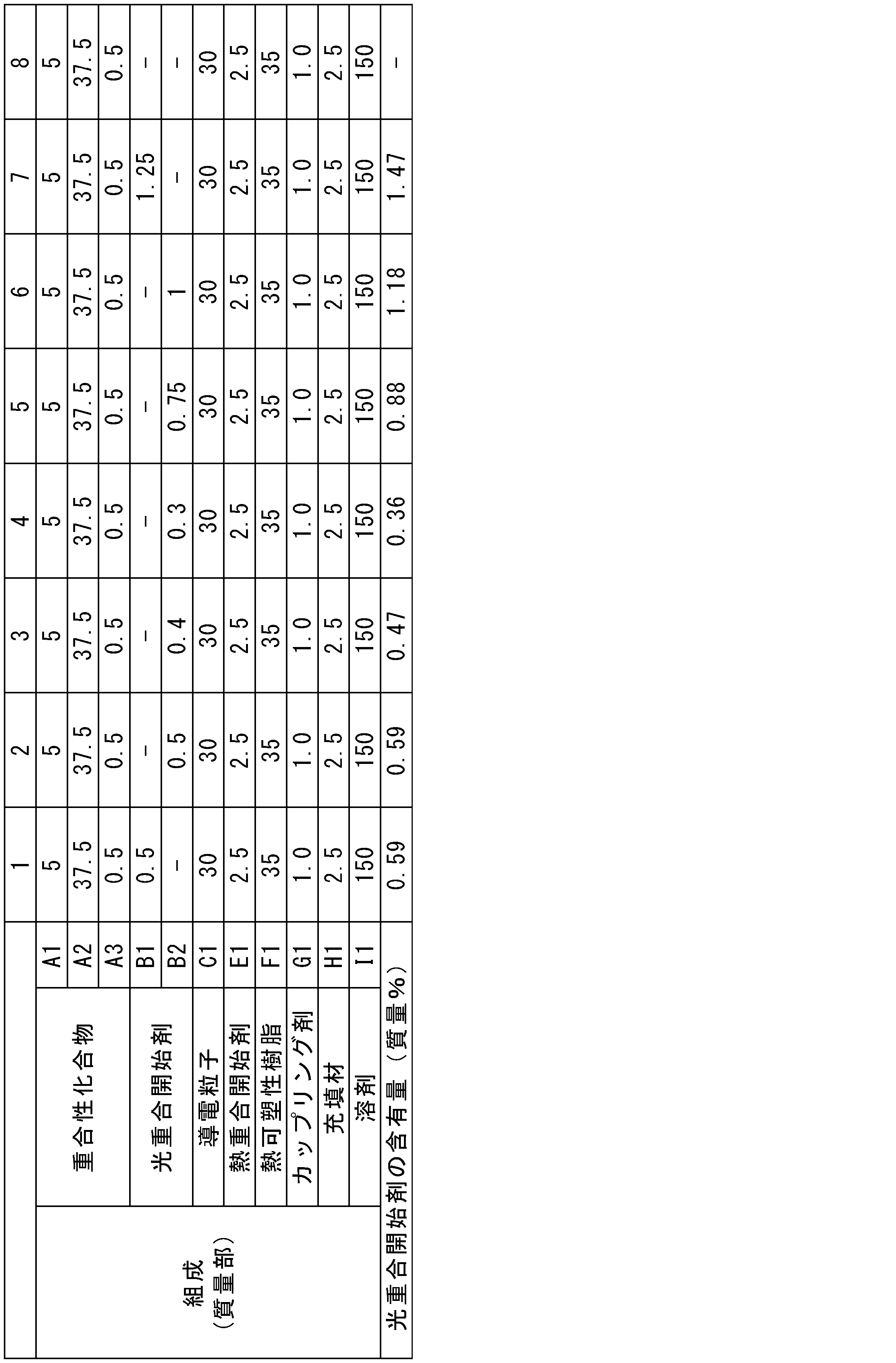
重合性化合物a1~a3、熱重合開始剤b1、カップリング剤g1、充填材h1及び溶剤i1として、光硬化性組成物における重合性化合物A1~A3、熱重合開始剤E1、カップリング剤G1、充填材H1及び溶剤I1と同じものを用い、熱可塑性樹脂f1は以下に示す成分を用い、これらの成分を表2に示す配合量(質量部)で混合し、熱硬化性組成物1のワニスを調製した。
(熱可塑性樹脂)
f1:フェノキシ樹脂(商品名:PKHC、ユニオンカーバイド社製)
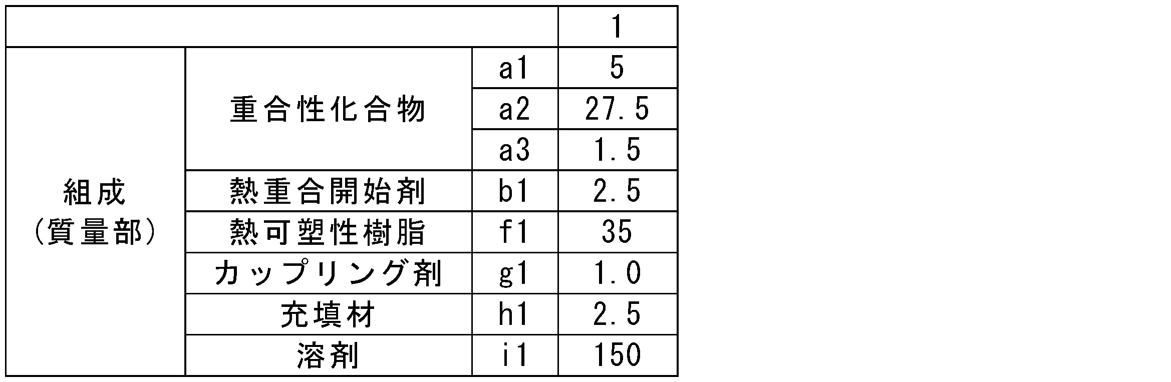
[第1の接着剤フィルムの作製]
光硬化性組成物1のワニスを、厚さ50μmのPETフィルム上に塗工装置を用いて塗布した。次いで、70℃、3分間の熱風乾燥を行い、PETフィルム上に厚さ(乾燥後の厚さ)が4μmの光硬化性組成物1からなる層を形成した。ここでの厚さは接触式厚み計を用いて測定した。なお、接触式厚み計を用いると導電粒子の大きさが反映され、導電粒子が存在する領域の厚みが測定される。そのため、第2の接着剤層を積層し、二層構成の回路接続用接着剤フィルムを作製した後に、後述の方法により、隣り合う導電粒子の離間部分に位置する第1の接着剤層の厚さを測定した。
熱硬化性組成物1のワニスを、厚さ50μmのPETフィルム上に塗工装置を用いて塗布した。次いで、70℃、3分間の熱風乾燥を行い、PETフィルム上に厚さが8μmの第2の接着剤層(熱硬化性組成物1からなる層)を形成した。以上の操作により、PETフィルム上に第2の接着剤層を備える第2の接着剤フィルムを得た。
第1の接着剤フィルムと第2の接着剤フィルムとを、それぞれの接着剤層が対向するように配置し、基材であるPETフィルムと共に40℃で加熱しながら、ロールラミネータでラミネートした。これにより、第1の接着剤層と第2の接着剤層とが積層された二層構成の回路接続用接着剤フィルムを作製した。
作製した回路接続用接着剤フィルムを介して、ピッチ25μmのCOF(FLEXSEED社製)と、ガラス基板上に非結晶酸化インジウム錫(ITO)からなる薄膜電極(高さ:1200Å)を備える、薄膜電極付きガラス基板(ジオマテック社製)とを、熱圧着装置(加熱方式:コンスタントヒート型、株式会社太陽機械製作所製)を用いて、170℃、6MPaで4秒間の条件で加熱加圧を行って幅1mmにわたり接続し、回路接続構造体(接続構造体)を作製した。なお、接続の際には、回路接続用接着剤フィルムにおける第1の接着剤層側の面がガラス基板と対向するように、回路接続用接着剤フィルムをガラス基板上に配置した。
[粒子流動性評価]
得られた回路接続構造体について、回路接続用接着剤フィルムの樹脂染み出し部分の粒子流動状態を顕微鏡(商品名:ECLIPSE L200、株式会社ニコン製)を用いて評価した。具体的には、作製した回路接続構造体をガラス基板側から、顕微鏡にて観察し、回路接続用接着剤フィルムの幅よりも外側に染み出した部分の粒子状態を3段階で評価した。粒子がほとんど動かず、染み出し部分に粒子がない状態を1、多少粒子が動いているが、粒子同士の連結がみられない状態を2、粒子が流動し、粒子同士の連結が見られる状態を3とした。
得られた回路接続構造体について、接続直後、及び、高温高湿試験後の対向する電極間の接続抵抗値を、マルチメーターで測定した。高温高湿試験は、85℃、85%RHの恒温恒湿槽に200h放置することにより行った。接続抵抗値は、対向する電極間の抵抗16点の平均値として求めた。
高温高湿試験後の回路接続構造体の回路接続部における剥離の有無を顕微鏡(商品名:ECLIPSE L200、株式会社ニコン製)を用いて評価した。具体的には、上述のとおり作製した回路接続構造体をガラス基板側から、顕微鏡にて観察し、ガラス基板と回路接続用接着剤フィルムとの剥離状態を3段階で評価した。回路接続用接着剤フィルム全体の面積のうち、ガラス基板から剥離している割合を求め、剥離がほとんど生じていない(剥離部分の割合が全体の5%未満以下)ものをA、剥離が少量生じている(剥離部分の割合が全体の5%以上20%未満)ものをB、剥離が生じている(剥離部分の割合が全体の20%以上)ものをCとした。
光硬化性組成物として、光硬化性組成物2~8を用いたこと以外は、実施例1と同様にして、回路接続用接着剤フィルム及び回路接続構造体を作製し、実施例1と同様にして、回路接続構造体の評価を行った。結果を表3及び表4に示す。
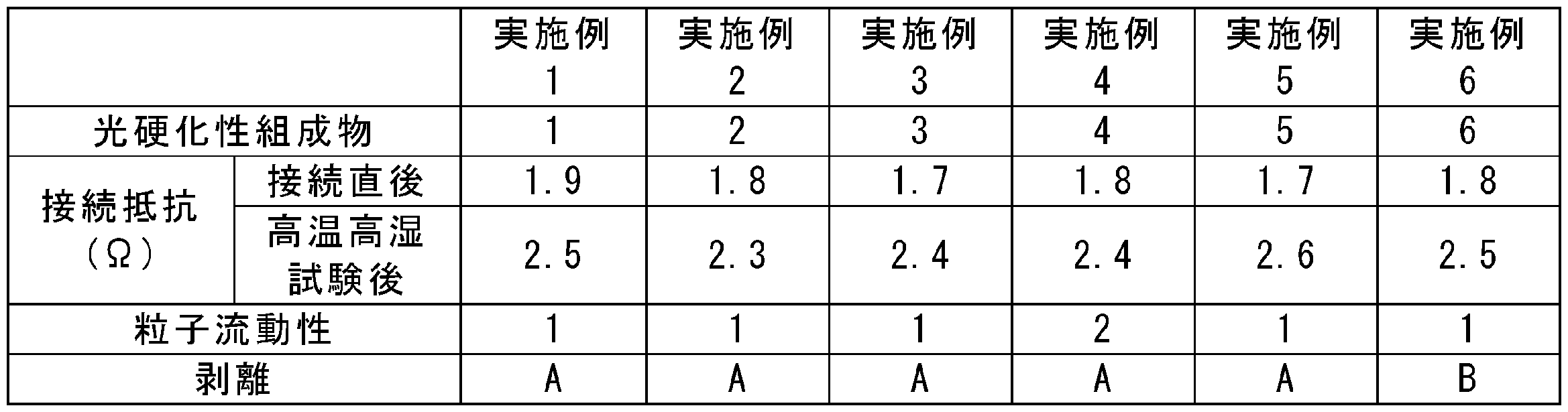
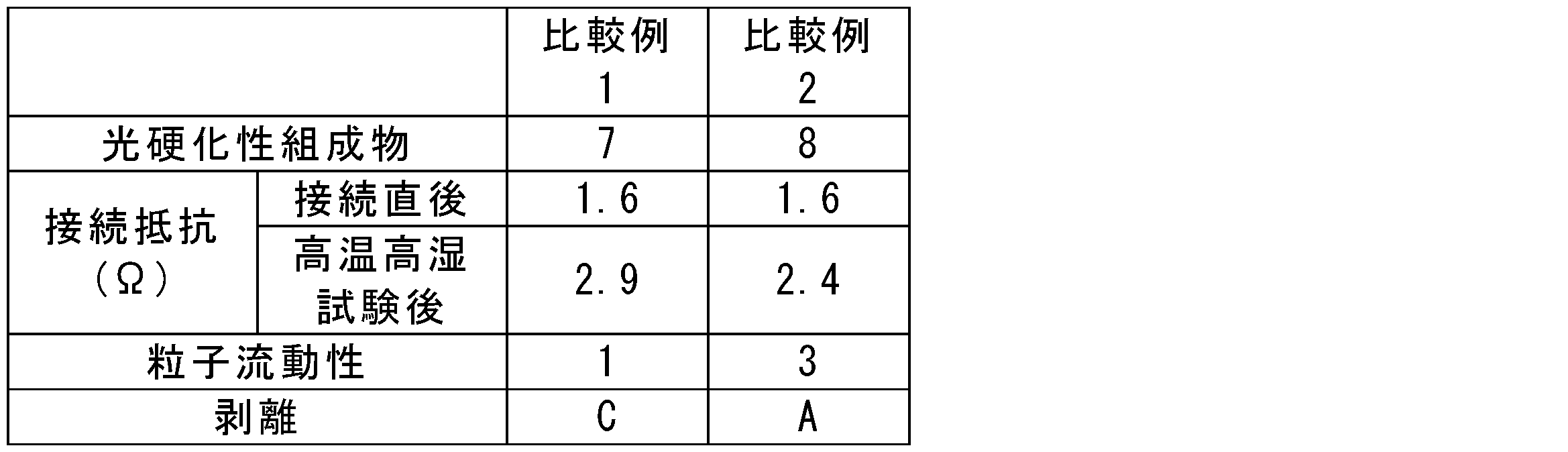
Claims (11)
- 第1の接着剤層と、該第1の接着剤層上に積層された第2の接着剤層と、を備え、
前記第1の接着剤層は光硬化性組成物の硬化物からなり、
前記第2の接着剤層は熱硬化性組成物からなり、
前記光硬化性組成物は、重合性化合物と、オキシムエステル構造を有する光重合開始剤と、導電粒子と、を含有し、
前記光重合開始剤の含有量は、前記光硬化性組成物中の導電粒子以外の成分の合計量を基準として、0.3~1.2質量%である、回路接続用接着剤フィルム。 - 前記重合性化合物は、ラジカル重合性基を有するラジカル重合性化合物である、請求項1に記載の回路接続用接着剤フィルム。
- 前記熱硬化性組成物は、ラジカル重合性基を有するラジカル重合性化合物を含有する、請求項1又は2に記載の回路接続用接着剤フィルム。
- 前記第1の接着剤層の厚さは、前記導電粒子の平均粒径の0.1~0.8倍である、請求項1~3のいずれか一項に記載の回路接続用接着剤フィルム。
- 前記オキシムエステル構造を有する光重合開始剤は、下記式(VI)で示される構造を有する化合物である、請求項1~4のいずれか一項に記載の回路接続用接着剤フィルム。

- 第1の接着剤層を用意する用意工程と、
前記第1の接着剤層上に熱硬化性組成物からなる第2の接着剤層を積層する積層工程と、を備え、
前記用意工程は、光硬化性組成物からなる層に対して光を照射することにより前記光硬化性組成物を硬化させ、前記第1の接着剤層を得る工程を含み、
前記光硬化性組成物は、重合性化合物と、オキシムエステル構造を有する光重合開始剤と、導電粒子と、を含有し、
前記光重合開始剤の含有量は、前記光硬化性組成物中の導電粒子以外の成分の合計量を基準として、0.3~1.2質量%である、回路接続用接着剤フィルムの製造方法。 - 前記重合性化合物は、ラジカル重合性基を有するラジカル重合性化合物である、請求項6に記載の回路接続用接着剤フィルムの製造方法。
- 前記熱硬化性組成物は、ラジカル重合性基を有するラジカル重合性化合物を含有する、請求項6又は7に記載の回路接続用接着剤フィルムの製造方法。
- 前記第1の接着剤層の厚さは、前記導電粒子の平均粒径の0.1~0.8倍である、請求項6~8のいずれか一項に記載の回路接続用接着剤フィルムの製造方法。
- 第1の電極を有する第1の回路部材と、第2の電極を有する第2の回路部材との間に、請求項1~5のいずれか一項に記載の回路接続用接着剤フィルムを介在させ、前記第1の回路部材及び前記第2の回路部材を熱圧着して、前記第1の電極及び前記第2の電極を互いに電気的に接続する工程を備える、回路接続構造体の製造方法。
- 請求項1~5のいずれか一項に記載の回路接続用接着剤フィルムと、該接着剤フィルムを収容する収容部材と、を備え、
前記収容部材は、前記収容部材の内部を外部から視認可能とする視認部を有し、
前記視認部における波長365nmの光の透過率は10%以下である、接着剤フィルム収容セット。
Priority Applications (3)
| Application Number | Priority Date | Filing Date | Title |
|---|---|---|---|
| JP2021505093A JP7480772B2 (ja) | 2019-03-13 | 2020-03-10 | 回路接続用接着剤フィルム及びその製造方法、回路接続構造体の製造方法、並びに、接着剤フィルム収容セット |
| KR1020217031909A KR102827331B1 (ko) | 2019-03-13 | 2020-03-10 | 회로 접속용 접착제 필름 및 그 제조 방법, 회로 접속 구조체의 제조 방법, 및, 접착제 필름 수용 세트 |
| CN202080019861.8A CN113557273B (zh) | 2019-03-13 | 2020-03-10 | 电路连接用黏合剂膜及其制造方法、电路连接结构体的制造方法以及黏合剂膜收纳套组 |
Applications Claiming Priority (2)
| Application Number | Priority Date | Filing Date | Title |
|---|---|---|---|
| JP2019046431 | 2019-03-13 | ||
| JP2019-046431 | 2019-03-13 |
Publications (1)
| Publication Number | Publication Date |
|---|---|
| WO2020184584A1 true WO2020184584A1 (ja) | 2020-09-17 |
Family
ID=72426624
Family Applications (1)
| Application Number | Title | Priority Date | Filing Date |
|---|---|---|---|
| PCT/JP2020/010387 Ceased WO2020184584A1 (ja) | 2019-03-13 | 2020-03-10 | 回路接続用接着剤フィルム及びその製造方法、回路接続構造体の製造方法、並びに、接着剤フィルム収容セット |
Country Status (5)
| Country | Link |
|---|---|
| JP (1) | JP7480772B2 (ja) |
| KR (1) | KR102827331B1 (ja) |
| CN (1) | CN113557273B (ja) |
| TW (1) | TWI899070B (ja) |
| WO (1) | WO2020184584A1 (ja) |
Citations (6)
| Publication number | Priority date | Publication date | Assignee | Title |
|---|---|---|---|---|
| JP2005144745A (ja) * | 2003-11-12 | 2005-06-09 | Hitachi Chem Co Ltd | 異方導電フィルム及びこれを用いた回路板 |
| WO2014021457A1 (ja) * | 2012-08-03 | 2014-02-06 | デクセリアルズ株式会社 | 異方性導電フィルム及びその製造方法 |
| JP2014210878A (ja) * | 2013-04-19 | 2014-11-13 | デクセリアルズ株式会社 | 異方性導電フィルム、接続方法、及び接合体 |
| JP2017171472A (ja) * | 2016-03-24 | 2017-09-28 | デクセリアルズ株式会社 | リール部材、及びフィルム巻装体 |
| JP2018119103A (ja) * | 2017-01-27 | 2018-08-02 | 日立化成株式会社 | 接着剤組成物、フィルム状接着剤、接続構造体及びその製造方法 |
| WO2019050006A1 (ja) * | 2017-09-11 | 2019-03-14 | 日立化成株式会社 | 回路接続用接着剤フィルム及びその製造方法、回路接続構造体の製造方法、並びに、接着剤フィルム収容セット |
Family Cites Families (1)
| Publication number | Priority date | Publication date | Assignee | Title |
|---|---|---|---|---|
| CN100537689C (zh) | 2003-12-04 | 2009-09-09 | 旭化成电子材料株式会社 | 各向异性的导电粘合片材及连接结构体 |
-
2020
- 2020-03-10 CN CN202080019861.8A patent/CN113557273B/zh active Active
- 2020-03-10 WO PCT/JP2020/010387 patent/WO2020184584A1/ja not_active Ceased
- 2020-03-10 JP JP2021505093A patent/JP7480772B2/ja active Active
- 2020-03-10 KR KR1020217031909A patent/KR102827331B1/ko active Active
- 2020-03-11 TW TW109107998A patent/TWI899070B/zh active
Patent Citations (6)
| Publication number | Priority date | Publication date | Assignee | Title |
|---|---|---|---|---|
| JP2005144745A (ja) * | 2003-11-12 | 2005-06-09 | Hitachi Chem Co Ltd | 異方導電フィルム及びこれを用いた回路板 |
| WO2014021457A1 (ja) * | 2012-08-03 | 2014-02-06 | デクセリアルズ株式会社 | 異方性導電フィルム及びその製造方法 |
| JP2014210878A (ja) * | 2013-04-19 | 2014-11-13 | デクセリアルズ株式会社 | 異方性導電フィルム、接続方法、及び接合体 |
| JP2017171472A (ja) * | 2016-03-24 | 2017-09-28 | デクセリアルズ株式会社 | リール部材、及びフィルム巻装体 |
| JP2018119103A (ja) * | 2017-01-27 | 2018-08-02 | 日立化成株式会社 | 接着剤組成物、フィルム状接着剤、接続構造体及びその製造方法 |
| WO2019050006A1 (ja) * | 2017-09-11 | 2019-03-14 | 日立化成株式会社 | 回路接続用接着剤フィルム及びその製造方法、回路接続構造体の製造方法、並びに、接着剤フィルム収容セット |
Also Published As
| Publication number | Publication date |
|---|---|
| JPWO2020184584A1 (ja) | 2020-09-17 |
| KR102827331B1 (ko) | 2025-06-27 |
| JP7480772B2 (ja) | 2024-05-10 |
| CN113557273B (zh) | 2023-06-16 |
| TWI899070B (zh) | 2025-10-01 |
| CN113557273A (zh) | 2021-10-26 |
| KR20210141954A (ko) | 2021-11-23 |
| TW202045665A (zh) | 2020-12-16 |
Similar Documents
| Publication | Publication Date | Title |
|---|---|---|
| JP7666535B2 (ja) | 回路接続用接着剤フィルム及びその製造方法、回路接続構造体の製造方法、並びに、接着剤フィルム収容セット | |
| JP7210846B2 (ja) | 回路接続用接着剤フィルム及びその製造方法、回路接続構造体の製造方法、並びに、接着剤フィルム収容セット | |
| JP7264054B2 (ja) | 回路接続用接着剤フィルム及びその製造方法、回路接続構造体の製造方法、並びに、接着剤フィルム収容セット | |
| KR102832635B1 (ko) | 회로 접속용 접착제 필름 및 그 제조 방법, 회로 접속 구조체의 제조 방법, 및, 접착제 필름 수용 세트 | |
| WO2022059647A1 (ja) | 回路接続用接着剤フィルム及びその製造方法、並びに、回路接続構造体の製造方法 | |
| JP2022020338A (ja) | 回路接続用接着剤フィルム及びその製造方法、並びに、回路接続構造体の製造方法 | |
| JP7480772B2 (ja) | 回路接続用接着剤フィルム及びその製造方法、回路接続構造体の製造方法、並びに、接着剤フィルム収容セット | |
| JP7468507B2 (ja) | 回路接続用接着剤フィルム及びその製造方法、回路接続構造体の製造方法、並びに、接着剤フィルム収容セット | |
| JP2022048791A (ja) | 回路接続用接着剤フィルム、並びに、回路接続構造体及びその製造方法 | |
| JP2022098985A (ja) | 回路接続用接着剤フィルム及びその製造方法、回路接続構造体の製造方法 | |
| JP2022039384A (ja) | 回路接続用接着剤フィルム及びその製造方法、並びに、回路接続構造体の製造方法 |
Legal Events
| Date | Code | Title | Description |
|---|---|---|---|
| 121 | Ep: the epo has been informed by wipo that ep was designated in this application |
Ref document number: 20768920 Country of ref document: EP Kind code of ref document: A1 |
|
| ENP | Entry into the national phase |
Ref document number: 2021505093 Country of ref document: JP Kind code of ref document: A |
|
| NENP | Non-entry into the national phase |
Ref country code: DE |
|
| ENP | Entry into the national phase |
Ref document number: 20217031909 Country of ref document: KR Kind code of ref document: A |
|
| 32PN | Ep: public notification in the ep bulletin as address of the adressee cannot be established |
Free format text: NOTING OF LOSS OF RIGHTS PURSUANT TO RULE 112(1) EPC (EPO FORM 1205A DATED 15.12.2021) |
|
| 122 | Ep: pct application non-entry in european phase |
Ref document number: 20768920 Country of ref document: EP Kind code of ref document: A1 |