WO2020184331A1 - 高分子分散型液晶装置及び高分子分散型液晶パネルの駆動方法 - Google Patents
高分子分散型液晶装置及び高分子分散型液晶パネルの駆動方法 Download PDFInfo
- Publication number
- WO2020184331A1 WO2020184331A1 PCT/JP2020/009145 JP2020009145W WO2020184331A1 WO 2020184331 A1 WO2020184331 A1 WO 2020184331A1 JP 2020009145 W JP2020009145 W JP 2020009145W WO 2020184331 A1 WO2020184331 A1 WO 2020184331A1
- Authority
- WO
- WIPO (PCT)
- Prior art keywords
- liquid crystal
- polymer
- dispersed liquid
- pair
- circuit
- Prior art date
- Legal status (The legal status is an assumption and is not a legal conclusion. Google has not performed a legal analysis and makes no representation as to the accuracy of the status listed.)
- Ceased
Links
Images




Classifications
-
- G—PHYSICS
- G02—OPTICS
- G02F—OPTICAL DEVICES OR ARRANGEMENTS FOR THE CONTROL OF LIGHT BY MODIFICATION OF THE OPTICAL PROPERTIES OF THE MEDIA OF THE ELEMENTS INVOLVED THEREIN; NON-LINEAR OPTICS; FREQUENCY-CHANGING OF LIGHT; OPTICAL LOGIC ELEMENTS; OPTICAL ANALOGUE/DIGITAL CONVERTERS
- G02F1/00—Devices or arrangements for the control of the intensity, colour, phase, polarisation or direction of light arriving from an independent light source, e.g. switching, gating or modulating; Non-linear optics
- G02F1/01—Devices or arrangements for the control of the intensity, colour, phase, polarisation or direction of light arriving from an independent light source, e.g. switching, gating or modulating; Non-linear optics for the control of the intensity, phase, polarisation or colour
- G02F1/13—Devices or arrangements for the control of the intensity, colour, phase, polarisation or direction of light arriving from an independent light source, e.g. switching, gating or modulating; Non-linear optics for the control of the intensity, phase, polarisation or colour based on liquid crystals, e.g. single liquid crystal display cells
- G02F1/133—Constructional arrangements; Operation of liquid crystal cells; Circuit arrangements
- G02F1/1333—Constructional arrangements; Manufacturing methods
- G02F1/1334—Constructional arrangements; Manufacturing methods based on polymer dispersed liquid crystals, e.g. microencapsulated liquid crystals
-
- G—PHYSICS
- G02—OPTICS
- G02F—OPTICAL DEVICES OR ARRANGEMENTS FOR THE CONTROL OF LIGHT BY MODIFICATION OF THE OPTICAL PROPERTIES OF THE MEDIA OF THE ELEMENTS INVOLVED THEREIN; NON-LINEAR OPTICS; FREQUENCY-CHANGING OF LIGHT; OPTICAL LOGIC ELEMENTS; OPTICAL ANALOGUE/DIGITAL CONVERTERS
- G02F1/00—Devices or arrangements for the control of the intensity, colour, phase, polarisation or direction of light arriving from an independent light source, e.g. switching, gating or modulating; Non-linear optics
- G02F1/01—Devices or arrangements for the control of the intensity, colour, phase, polarisation or direction of light arriving from an independent light source, e.g. switching, gating or modulating; Non-linear optics for the control of the intensity, phase, polarisation or colour
- G02F1/13—Devices or arrangements for the control of the intensity, colour, phase, polarisation or direction of light arriving from an independent light source, e.g. switching, gating or modulating; Non-linear optics for the control of the intensity, phase, polarisation or colour based on liquid crystals, e.g. single liquid crystal display cells
- G02F1/133—Constructional arrangements; Operation of liquid crystal cells; Circuit arrangements
- G02F1/13306—Circuit arrangements or driving methods for the control of single liquid crystal cells
-
- G—PHYSICS
- G02—OPTICS
- G02F—OPTICAL DEVICES OR ARRANGEMENTS FOR THE CONTROL OF LIGHT BY MODIFICATION OF THE OPTICAL PROPERTIES OF THE MEDIA OF THE ELEMENTS INVOLVED THEREIN; NON-LINEAR OPTICS; FREQUENCY-CHANGING OF LIGHT; OPTICAL LOGIC ELEMENTS; OPTICAL ANALOGUE/DIGITAL CONVERTERS
- G02F1/00—Devices or arrangements for the control of the intensity, colour, phase, polarisation or direction of light arriving from an independent light source, e.g. switching, gating or modulating; Non-linear optics
- G02F1/01—Devices or arrangements for the control of the intensity, colour, phase, polarisation or direction of light arriving from an independent light source, e.g. switching, gating or modulating; Non-linear optics for the control of the intensity, phase, polarisation or colour
- G02F1/13—Devices or arrangements for the control of the intensity, colour, phase, polarisation or direction of light arriving from an independent light source, e.g. switching, gating or modulating; Non-linear optics for the control of the intensity, phase, polarisation or colour based on liquid crystals, e.g. single liquid crystal display cells
- G02F1/133—Constructional arrangements; Operation of liquid crystal cells; Circuit arrangements
- G02F1/1333—Constructional arrangements; Manufacturing methods
- G02F1/1343—Electrodes
- G02F1/13439—Electrodes characterised by their electrical, optical, physical properties; materials therefor; method of making
-
- G—PHYSICS
- G02—OPTICS
- G02F—OPTICAL DEVICES OR ARRANGEMENTS FOR THE CONTROL OF LIGHT BY MODIFICATION OF THE OPTICAL PROPERTIES OF THE MEDIA OF THE ELEMENTS INVOLVED THEREIN; NON-LINEAR OPTICS; FREQUENCY-CHANGING OF LIGHT; OPTICAL LOGIC ELEMENTS; OPTICAL ANALOGUE/DIGITAL CONVERTERS
- G02F1/00—Devices or arrangements for the control of the intensity, colour, phase, polarisation or direction of light arriving from an independent light source, e.g. switching, gating or modulating; Non-linear optics
- G02F1/01—Devices or arrangements for the control of the intensity, colour, phase, polarisation or direction of light arriving from an independent light source, e.g. switching, gating or modulating; Non-linear optics for the control of the intensity, phase, polarisation or colour
- G02F1/13—Devices or arrangements for the control of the intensity, colour, phase, polarisation or direction of light arriving from an independent light source, e.g. switching, gating or modulating; Non-linear optics for the control of the intensity, phase, polarisation or colour based on liquid crystals, e.g. single liquid crystal display cells
- G02F1/137—Devices or arrangements for the control of the intensity, colour, phase, polarisation or direction of light arriving from an independent light source, e.g. switching, gating or modulating; Non-linear optics for the control of the intensity, phase, polarisation or colour based on liquid crystals, e.g. single liquid crystal display cells characterised by the electro-optical or magneto-optical effect, e.g. field-induced phase transition, orientation effect, guest-host interaction or dynamic scattering
-
- G—PHYSICS
- G02—OPTICS
- G02F—OPTICAL DEVICES OR ARRANGEMENTS FOR THE CONTROL OF LIGHT BY MODIFICATION OF THE OPTICAL PROPERTIES OF THE MEDIA OF THE ELEMENTS INVOLVED THEREIN; NON-LINEAR OPTICS; FREQUENCY-CHANGING OF LIGHT; OPTICAL LOGIC ELEMENTS; OPTICAL ANALOGUE/DIGITAL CONVERTERS
- G02F1/00—Devices or arrangements for the control of the intensity, colour, phase, polarisation or direction of light arriving from an independent light source, e.g. switching, gating or modulating; Non-linear optics
- G02F1/01—Devices or arrangements for the control of the intensity, colour, phase, polarisation or direction of light arriving from an independent light source, e.g. switching, gating or modulating; Non-linear optics for the control of the intensity, phase, polarisation or colour
- G02F1/13—Devices or arrangements for the control of the intensity, colour, phase, polarisation or direction of light arriving from an independent light source, e.g. switching, gating or modulating; Non-linear optics for the control of the intensity, phase, polarisation or colour based on liquid crystals, e.g. single liquid crystal display cells
- G02F1/133—Constructional arrangements; Operation of liquid crystal cells; Circuit arrangements
- G02F1/1333—Constructional arrangements; Manufacturing methods
- G02F1/1345—Conductors connecting electrodes to cell terminals
- G02F1/13452—Conductors connecting driver circuitry and terminals of panels
-
- G—PHYSICS
- G09—EDUCATION; CRYPTOGRAPHY; DISPLAY; ADVERTISING; SEALS
- G09G—ARRANGEMENTS OR CIRCUITS FOR CONTROL OF INDICATING DEVICES USING STATIC MEANS TO PRESENT VARIABLE INFORMATION
- G09G2320/00—Control of display operating conditions
- G09G2320/02—Improving the quality of display appearance
- G09G2320/0247—Flicker reduction other than flicker reduction circuits used for single beam cathode-ray tubes
-
- G—PHYSICS
- G09—EDUCATION; CRYPTOGRAPHY; DISPLAY; ADVERTISING; SEALS
- G09G—ARRANGEMENTS OR CIRCUITS FOR CONTROL OF INDICATING DEVICES USING STATIC MEANS TO PRESENT VARIABLE INFORMATION
- G09G3/00—Control arrangements or circuits, of interest only in connection with visual indicators other than cathode-ray tubes
- G09G3/20—Control arrangements or circuits, of interest only in connection with visual indicators other than cathode-ray tubes for presentation of an assembly of a number of characters, e.g. a page, by composing the assembly by combination of individual elements arranged in a matrix no fixed position being assigned to or needed to be assigned to the individual characters or partial characters
- G09G3/34—Control arrangements or circuits, of interest only in connection with visual indicators other than cathode-ray tubes for presentation of an assembly of a number of characters, e.g. a page, by composing the assembly by combination of individual elements arranged in a matrix no fixed position being assigned to or needed to be assigned to the individual characters or partial characters by control of light from an independent source
- G09G3/36—Control arrangements or circuits, of interest only in connection with visual indicators other than cathode-ray tubes for presentation of an assembly of a number of characters, e.g. a page, by composing the assembly by combination of individual elements arranged in a matrix no fixed position being assigned to or needed to be assigned to the individual characters or partial characters by control of light from an independent source using liquid crystals
- G09G3/3611—Control of matrices with row and column drivers
- G09G3/3614—Control of polarity reversal in general
Definitions
- the present invention relates to a polymer-dispersed liquid crystal device and a method for driving a polymer-dispersed liquid crystal panel.
- Patent Document 1 a polymer-dispersed liquid crystal panel having a liquid crystal layer in which a polymer-dispersed liquid crystal is filled between a pair of transparent electrodes is known (see, for example, Patent Document 1).
- the polymer-dispersed liquid crystal panel in a state where an AC voltage is not applied to the pair of transparent electrodes, the arrangement of the liquid crystal molecules becomes an irregular state, and the light is scattered (scattered state). As a result, the polymer-dispersed liquid crystal panel can be completely whitened so that the other side cannot be visually recognized from one side.
- the polymer-dispersed liquid crystal panel by applying an AC voltage to a pair of transparent electrodes, the arrangement of the liquid crystal molecules contained in the polymer-dispersed liquid crystal becomes regular, and light is transmitted. It becomes a state (non-scattering state).
- Such a polymer-dispersed liquid crystal panel can be formed into a film, it is used as a light control film. For example, by attaching a polymer-dispersed liquid crystal panel to an existing window glass, it can function as a blind shutter.
- the conventional polymer dispersion type liquid crystal device can be driven by a commercial AC power supply that can be easily used in homes and offices.
- driving by a commercial AC power source has a problem that the frequency is short, so that the power consumption is large and the environmental load is large. Further, since the frequency of the commercial AC power supply differs depending on the region, there is a problem that the voltage is not stable.
- An object of the present invention is to provide a polymer-dispersed liquid crystal display and a method for driving a polymer-dispersed liquid crystal panel, which enable stable driving with low power consumption.
- the polymer-dispersed liquid crystal apparatus of the present invention between a pair of transparent substrates, a pair of transparent electrodes provided between the pair of transparent substrates, and between the pair of transparent electrodes.
- a polymer comprising a liquid crystal layer filled with a polymer-dispersed liquid crystal and a drive circuit that puts the liquid crystal layer in a non-scattering state or a scattered state by applying a voltage between the pair of transparent electrodes.
- the drive circuit is characterized in that a DC voltage whose polarity is periodically inverted is applied between the pair of transparent electrodes.
- FIG. 3 is a cross-sectional view taken along the line AA of the polymer-dispersed liquid crystal panel shown in FIG.
- FIG. 3 is a sectional view taken along line BB of the polymer-dispersed liquid crystal panel shown in FIG.
- It is a figure which shows an example of the structure of a drive circuit. It is a figure which shows an example of the structure of the 1st current limiting circuit.
- FIG. 12 is a cross-sectional view taken along the line AA of the polymer-dispersed liquid crystal panel shown in FIG.
- the width direction of the polymer-dispersed liquid crystal apparatus 10 when viewed from the front side is the X-axis direction
- the depth direction is the Y-axis direction
- the height direction is the Z-axis direction.
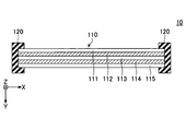
- FIG. 1 is a front view of the polymer-dispersed liquid crystal apparatus 10 according to the embodiment of the present invention.
- the polymer-dispersed liquid crystal apparatus 10 shown in FIG. 1 is a flat plate-shaped and rectangular apparatus.
- the polymer-dispersed liquid crystal device 10 has a rectangular and transparent polymer-dispersed liquid crystal panel 110, and is in a state of transmitting light by driving the polymer-dispersed liquid crystal panel 110 (hereinafter, non-polymer dispersion type liquid crystal panel 110).
- the polymer-dispersed liquid crystal device 10 functions as a blind shutter for the window 20 by being attached to the window 20.
- the polymer-dispersed liquid crystal device 10 includes a polymer-dispersed liquid crystal panel 110, a frame 120, a battery 130, and a drive circuit 140.
- the polymer-dispersed liquid crystal panel 110 is a flat plate-shaped and rectangular member, and when driven by the drive circuit 140, the light transmission characteristic is switched between the non-scattering state and the scattered state.
- the polymer-dispersed liquid crystal panel 110 when a driving voltage is applied from the drive circuit 140, the arrangement of liquid crystal molecules contained in the polymer-dispersed liquid crystal becomes regular, and light is transmitted. It becomes a non-scattering state.
- the polymer-dispersed liquid crystal panel 110 when a driving voltage is not applied from the driving circuit 140, the liquid crystal molecules are arranged irregularly, and the light is scattered.
- the polymer-dispersed liquid crystal panel 110 is completely whitened in a state of scattering light. In the scattered state, the polymer-dispersed liquid crystal panel 110 cannot visually recognize the other side from one side in the depth direction (Y-axis direction in the drawing).
- the frame 120 is provided with a constant width and a constant thickness along the outer peripheral edge of the polymer-dispersed liquid crystal panel 110 (that is, the four sides of the polymer-dispersed liquid crystal panel 110). It is a member of the shape.
- the external dimensions of the frame 120 are substantially the same as the internal dimensions of the sash 22 as the window frame included in the window 20. As a result, the polymer-dispersed liquid crystal apparatus 10 can be easily attached to the window 20 in a state of being overlapped with the window glass 24 included in the window 20 by being fitted inside the sash 22.
- the battery 130 supplies a DC voltage to the drive circuit 140.
- various secondary batteries for example, a lithium ion battery, a lithium polymer battery, etc. can be used.
- the drive circuit 140 generates a drive voltage when the polymer-dispersed liquid crystal panel 110 is placed in a non-scattering state. Specifically, the drive circuit 140 generates a DC drive voltage that is higher than the voltage generated by the battery 130 and whose polarity changes periodically.
- the drive circuit 140 drives the polymer-dispersed liquid crystal panel 110 by applying the generated drive voltage between the pair of transparent electrodes 112 and 114, which will be described later.
- the polymer-dispersed liquid crystal panel 110 switches from a scattered state to a non-scattered state when a driving voltage is applied from the driving circuit 140.
- the drive circuit 140 has a connection terminal 148 to which a charging cable is connected. The battery 130 is charged by the electric power supplied from the charging cable via the connection terminal 148.
- FIG. 2 is a cross-sectional view taken along the line AA of the polymer-dispersed liquid crystal apparatus 10 shown in FIG.
- the polymer-dispersed liquid crystal panel 110 has a laminated structure in which a plurality of flat plate-shaped constituent parts are laminated. Further, in the polymer-dispersed liquid crystal panel 110, the outer peripheral edge portion is sandwiched by the frame 120.
- the polymer-dispersed liquid crystal panel 110 has a transparent substrate 111, a transparent electrode 112, a liquid crystal layer 113, a transparent electrode 114, and a transparent substrate 115 in this order from the front side (Y-axis negative side in the drawing). It has a laminated structure in which these constituent parts 111 to 115 are laminated.
- the pair of transparent substrates 111 and 115 are transparent and flat members having a rectangular shape in a plan view from the front side (Y-axis negative side in the drawing).
- the transparent substrate 111 is provided on the front surface of the polymer-dispersed liquid crystal panel 110.
- the transparent substrate 115 is provided on the innermost back surface of the polymer-dispersed liquid crystal panel 110.
- a PET (polyethylene terephthalate) resin plate, a glass plate, or the like can be used as the transparent substrates 111 and 115.
- the pair of transparent electrodes 112 and 114 are conductive, transparent and thin-film constituents.
- the transparent electrode 112 is provided between the transparent substrate 111 and the transparent substrate 115 so as to overlap the transparent substrate 111.
- the transparent electrode 114 is provided between the transparent substrate 111 and the transparent substrate 115 so as to overlap the transparent substrate 115.
- the transparent electrode 112 is electrically connected to the drive circuit 140 by wiring 151 (see FIG. 1).
- the transparent electrode 114 is electrically connected to the drive circuit 140 by wiring 152 (see FIG. 1).
- a drive voltage is applied to the transparent electrodes 112 and 114 from the drive circuit 140 via the wirings 151 and 152.
- ITO Indium Tin Oxide
- the liquid crystal layer 113 is a constituent portion formed between the transparent electrode 112 and the transparent electrode 114.
- the liquid crystal layer 113 is formed by filling the gap between the transparent electrode 112 and the transparent electrode 114 with a polymer-dispersed liquid crystal.
- the liquid crystal layer 113 is in a scattered state when a driving voltage is not applied between the transparent electrodes 112 and 114.
- the liquid crystal layer 113 is in a non-scattering state when a driving voltage is applied between the transparent electrodes 112 and 114.
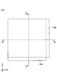
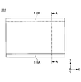
- FIG. 3 is a front view of the polymer-dispersed liquid crystal panel 110.
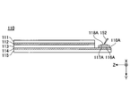
- FIG. 4 is a cross-sectional view taken along the line AA of the polymer-dispersed liquid crystal panel 110 shown in FIG.
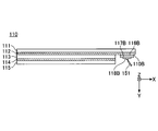
- FIG. 5 is a cross-sectional view taken along the line BB of the polymer-dispersed liquid crystal panel 110 shown in FIG.
- the left edge portion (the edge portion on the negative side of the X axis in the drawing) on the front side (negative side of the Y axis in the drawing) of the polymer-dispersed liquid crystal panel 110 has the left edge portion.
- a first exposed portion 110A is formed so as to extend with a certain width along the above.
- the first exposed portion 110A is a portion where a part of the front surface of the transparent electrode 114 is exposed by partially removing the transparent substrate 111, the transparent electrode 112, and the liquid crystal layer 113.
- a copper foil layer 117A is formed on the surface of the transparent electrode 114 in the first exposed portion 110A via the silver paste layer 116A.
- One end of the above-mentioned wiring 152 made of a lead wire is connected to the copper foil layer 117A by using solder 118A.
- the other end of the wiring 152 is connected to the drive circuit 140.
- the left side of the lower edge portion (the edge portion on the negative side of the Z axis in the drawing) on the back side (the positive side of the Y axis in the drawing) of the polymer-dispersed liquid crystal panel 110 A second exposed portion 110B is formed that extends along the edge portion with a constant width.
- the second exposed portion 110B is a portion where a part of the back surface side of the transparent electrode 112 is exposed by partially removing the liquid crystal layer 113, the transparent electrode 114, and the transparent substrate 115.
- a copper foil layer 117B is formed on the surface of the transparent electrode 112 in the second exposed portion 110B via the silver paste layer 116B.
- One end of the above-mentioned wiring 151 made of a lead wire is connected to the copper foil layer 117B by using solder 118B.
- the other end of the wiring 151 is connected to the drive circuit 140.
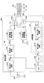
- FIG. 6 is a diagram showing an example of the configuration of the drive circuit 140.
- the drive circuit 140 includes a booster circuit 141, a first current limiting circuit 142, a switch circuit 143, a second current limiting circuit 144, a low dropout regulator (LDO) 145, and a clock circuit (CLK) 146. And a frequency dividing circuit 147 is provided.
- the booster circuit 141 includes a first booster circuit 141A and a second booster circuit 141B.
- the first booster circuit 141A and the second booster circuit 141B are each composed of a charge pump that raises (boosts) the voltage by combining a capacitor and a switch.
- the first booster circuit 141A is connected to the battery 130 and boosts the DC voltage generated by the battery 130. For example, when the DC voltage generated by the battery 130 is 3.6V, the first booster circuit 141A boosts the 3.6V DC voltage to a 16V DC voltage.
- the second booster circuit 141B is connected to the subsequent stage of the first booster circuit 141A, and further boosts the DC voltage boosted by the first booster circuit 141A. For example, the second booster circuit 141B boosts the 16V DC voltage output from the first booster circuit 141A to a 100V DC voltage. As a result, a DC voltage of, for example, 100 V is output from the booster circuit 141.
- the booster circuit 141 is connected to the transparent electrode 112 or the transparent electrode 114 of the polymer-dispersed liquid crystal panel 110 via the first current limiting circuit 142 and the switch circuit 143.
- the first current limiting circuit 142 is connected to the subsequent stage of the booster circuit 141, and is a circuit that limits the current flowing through the transparent electrode 112 or the transparent electrode 114 as a load to a predetermined current value or less. For example, the first current limiting circuit 142 limits the current flowing through the transparent electrode 112 or the transparent electrode 114 to 100 mA or less.
- the second current limiting circuit 144 is connected to the transparent electrode 112 or the transparent electrode 114 of the polymer-dispersed liquid crystal panel 110 via the switch circuit 143.
- the second current limiting circuit 144 is a circuit connected to the ground and limits the current flowing through the transparent electrode 112 or the transparent electrode 114 as a load to a predetermined current value or less. For example, the second current limiting circuit 144 limits the current flowing through the transparent electrode 112 or the transparent electrode 114 to 100 mA or less.
- the switch circuit 143 has a first switch 143A and a second switch 143B.
- One end of the first switch 143A is connected to the transparent electrode 112 via the wiring 151.
- the other end of the first switch 143A is connected to the first current limiting circuit 142 or the second current limiting circuit 144 according to a switching signal described later.
- One end of the second switch 143B is connected to the transparent electrode 114 via the wiring 152.
- the other end of the second switch 143B is connected to the first current limiting circuit 142 or the second current limiting circuit 144 according to a switching signal described later.
- the LDO 145 is a linear regulator having a low minimum potential difference required between input and output, and the output voltage (for example, 16V) of the first booster circuit 141A included in the booster circuit 141 is input as an input voltage.
- the LDO 145 steps down (drops out) the input voltage to produce a stable output voltage (eg, 5V) that is lower than the input.
- the CLK146 is connected to the subsequent stage of LDO145.
- the CLK146 has an oscillation circuit and generates a rectangular wave-shaped reference clock signal based on the output voltage from the LDO 145.
- the frequency (clock frequency) of the reference clock signal generated by the CLK146 is, for example, 2 Hz.
- the frequency dividing circuit 147 includes a first frequency dividing circuit 147A and a second frequency dividing circuit 147B.
- the first frequency dividing circuit 147A and the second frequency dividing circuit 147B are frequency conversion circuits that convert the frequency of the input signal to 1 times an integer, respectively.
- the first frequency dividing circuit 147A is connected to the subsequent stage of the CLK146, and is a 1/4 frequency dividing circuit that outputs the reference clock signal output by the CLK146 by multiplying the frequency by 1/4. For example, when the frequency of the reference clock signal is 2 Hz, the first frequency dividing circuit 147A outputs a clock signal having a frequency of 0.5 Hz.
- the second frequency dividing circuit 147B is connected to the subsequent stage of the first frequency dividing circuit 147A, and outputs the clock signal output by the first frequency dividing circuit 147A by multiplying the frequency by 1/10. It is a circuit. For example, when the frequency of the clock signal output from the first frequency dividing circuit 147A is 0.5 Hz, the second frequency dividing circuit 147B outputs a clock signal having a frequency of 0.05 Hz. The clock signal output from the second frequency dividing circuit 147B is input to the switch circuit 143 as a switching signal.
- the switch circuit 143 Based on the input switching signal, the switch circuit 143 sets the connection states of the first switch 143A and the second switch 143B to the first state represented by the solid line and the second state represented by the broken line shown in FIG. Switch between.
- the first state is a state in which the first switch 143A connects the wiring 151 to the first current limiting circuit 142, and the second switch 143B connects the wiring 152 to the second current limiting circuit 144.
- a voltage of 100 V is applied to the transparent electrode 112
- a ground potential (0 V) is applied to the transparent electrode 114.
- the second state is a state in which the first switch 143A connects the wiring 151 to the second current limiting circuit 144, and the second switch 143B connects the wiring 152 to the first current limiting circuit 142.
- a voltage of 100 V is applied to the transparent electrode 114, and a ground potential (0 V) is applied to the transparent electrode 112.
- the switch circuit 143 switches between the first state and the second state (polarity inversion) every 10 seconds.
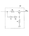
- FIG. 7 is a diagram showing an example of the configuration of the first current limiting circuit 142.
- the first current limiting circuit 142 has a pnp type transistor Q1, a diode D1, a diode D2, a resistor R1, and a resistor Rs.
- One end of the resistor R1 is connected to the base of the transistor Q1, and the other end is connected to the ground.
- One end of the resistor Rs is connected to the emitter of the transistor Q1.
- the diode D1 and the diode D2 are connected in series, and the cathode side of the diode D2 is connected to the base of the transistor Q1.
- the anode side of the diode D1 is connected to the other end of the resistor Rs.
- the other end of the resistor Rs is connected to the booster circuit 141, and the collector of the transistor Q1 is connected to the switch circuit 143.
- the output current I OUT output from the first current limiting circuit 142 is limited to the maximum current value I max calculated by the following equation (1).
- V DI the forward voltage drop (about 0.6 V) of the diode D1.
- the maximum current value I max can be determined by selecting the resistance value of the resistors Rs. For example, in order to set the maximum current value I max to 100 mA, a resistor Rs of 6 ⁇ may be used.
- the configuration of the second current limiting circuit 144 is the same as the configuration of the first current limiting circuit 142 shown in FIG. 7, the description thereof will be omitted.
- FIG. 8 is a diagram illustrating a waveform such as a drive voltage.
- FIG. 8A illustrates the waveform of the switching signal input to the switch circuit 143.
- FIG. 8B illustrates the waveform of the first drive voltage applied to the transparent electrode 112 as the first transparent electrode.
- FIG. 8C illustrates the waveform of the second drive voltage applied to the transparent electrode 114 as the second transparent electrode.
- FIG. 8D illustrates the light transmittance of the polymer-dispersed liquid crystal panel 110.
- FIG. 8E illustrates changes in the current flowing through the first and second transparent electrodes.
- the above-mentioned switching signal is a rectangular waveform having a predetermined period.
- the polarities of the first drive voltage and the second drive voltage are periodically inverted according to the rise and fall of the switching signal, respectively.
- This polarity reversal period T is 1/2 times the period of the switching signal.
- the voltage transition time ⁇ of the first drive voltage and the second drive voltage at the time of polarity reversal is defined as the time from the start of the voltage change to the arrival of the target value.
- the voltage transition time ⁇ is mainly determined by the time constant due to the resistance component and the capacitance component included in the first current limiting circuit 142 and the second current limiting circuit 144.
- flicker occurs due to a temporary decrease in the light transmittance of the polymer-dispersed liquid crystal panel 110 in response to the polarity reversal of the first drive voltage and the second drive voltage. Occurs. This flicker becomes smaller as the voltage transition time ⁇ becomes smaller. Further, the flicker is quantified by the flicker rate R (%) represented by the following formula (2).
- L max and L min are the maximum and minimum values of the brightness of the transmitted light when the polymer-dispersed liquid crystal panel 110 is irradiated with light of a constant brightness.
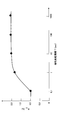
- FIG. 9 is a graph (experimental data) showing the relationship between the polarity reversal period T and the minimum value R min of the flicker rate R at which the subject visually recognizes the flicker.
- the minimum value R min of the flicker rate R is defined as the minimum flicker rate R in which flicker is visually recognized when two or more of the five subjects feel flicker.
- the minimum value R min increases accordingly.
- the rate of change of the minimum value R min decreases, and when the polarity reversal period T exceeds 10 seconds, it becomes a constant value at about 2%. This is because even if the subject stares at the polymer-dispersed liquid crystal panel 110 and observes it, the eyes blink after 10 seconds, so even if flicker occurs in the polymer-dispersed liquid crystal panel 110. This is because it doesn't bother me.
- the polarity reversal period T is preferably 1 second or longer.
- the frequency of the switching signal may be 0.5 Hz or less.
- the polarity reversal period T is preferably in the range of 1 second or more and 2 hours or less as a practical range.
- the polarity reversal period T is more preferably in the range of 1 second or more and 1 hour or less, and further preferably in the range of 1 second or more and 30 minutes or less.
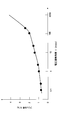
- FIG. 10 is a graph (experimental data) showing the relationship between the flicker rate R and the voltage transition time ⁇ . As shown in FIG. 10, it can be seen that the larger the voltage transition time ⁇ , the larger the flicker rate R. Further, from FIG. 10, it can be seen that the flicker rate R has a substantially constant increase rate until the voltage transition time ⁇ reaches 100 milliseconds, but the increase rate increases after 100 milliseconds. The flicker rate R is about 2% when the voltage transition time ⁇ is 100 milliseconds.
- the voltage transition time ⁇ may be set to 100 milliseconds or less. Further, it is more preferable that the voltage transition time ⁇ is 50 milliseconds or less, and it is further preferable that the voltage transition time ⁇ is 20 milliseconds or less.
- the time constants of the first current limiting circuit 142 and the second current limiting circuit 144 are set to 100 milliseconds or less, respectively.
- FIG. 11 is a diagram illustrating an equivalent circuit of the polymer-dispersed liquid crystal panel 110.
- the capacitance value and resistance value shown in FIG. 11 are numerical values when one side of the polymer-dispersed liquid crystal panel 110 is 1 meter (area is 1 m 2 ), and the time constant of the equivalent circuit is 3 milliseconds. Is.
- the first transparent electrode or the second transparent electrode can be started up to 100 V in 10 milliseconds with a current of 100 mA.
- the maximum current value I max of the first current limiting circuit 142 and the second current limiting circuit 144 is preferably 100 mA or less. Further, the maximum current value I max is more preferably 80 mA or less, and further preferably 60 mA or less.
- Table 1 is a diagram illustrating the dependence of power consumption on the polarity reversal period T.
- Table 1 is a calculated value of power consumption calculated for a plurality of polarity reversal periods T based on the equivalent circuit shown in FIG. As shown in Table 1, the power consumption decreases as the polarity reversal cycle T is lengthened, but tends to saturate when the polarity reversal cycle T is 10 seconds or longer.
- Table 1 shows the power consumption when the first and second transparent electrodes are driven by an AC voltage of a sine wave (60 Hz) as a comparative example. It can be seen that the power consumption is significantly reduced by using the rectangular DC voltage as in the present embodiment. Further, as the power consumption decreases, the driveable time of the polymer-dispersed liquid crystal apparatus 10 increases.
- the outer shape of the polymer-dispersed liquid crystal panel 110 is substantially square, but the shape of the polymer-dispersed liquid crystal panel 110 is not limited to this, and may be changed as appropriate.
- FIG. 12 is a diagram illustrating a polymer-dispersed liquid crystal panel 110 having a rectangular outer shape.
- FIG. 13 is a sectional view taken along the line AA of the polymer-dispersed liquid crystal panel 110 shown in FIG.
- the side parallel to the X direction is the long side
- the side parallel to the Z direction is the short side.
- the first exposed portion 110A and the second exposed portion 110B are formed at positions facing the long side direction and the short side direction. It is preferable to do so.
- the current generated when the polarity of the drive voltage is reversed by connecting the drive circuit 140 to the first exposed portion 110A and the second exposed portion 110B formed along the long side via the wirings 151 and 152. Concentration can be suppressed.
- the voltage transition time ⁇ at the time of polarity reversal is set by the time constants of the first current limiting circuit 142 and the second current limiting circuit 144, but the voltage transition time is set by separately providing a CR circuit or the like. ⁇ may be set.
- circuit configurations of the first current limiting circuit 142 and the second current limiting circuit 144 shown in FIG. 7 are merely examples, and a current limiting circuit having another circuit configuration using a diode or the like may be used.
- the polymer-dispersed liquid crystal panel a normal type polymer-dispersed liquid crystal that becomes transparent when a voltage is applied and becomes a scattered state when a non-voltage is applied is used. It is also possible to use a reverse type polymer dispersed liquid crystal display that is in a scattered state when a voltage is applied and is in a non-scattered state when a non-voltage is applied.
Landscapes
- Physics & Mathematics (AREA)
- Nonlinear Science (AREA)
- Chemical & Material Sciences (AREA)
- General Physics & Mathematics (AREA)
- Crystallography & Structural Chemistry (AREA)
- Optics & Photonics (AREA)
- Mathematical Physics (AREA)
- Engineering & Computer Science (AREA)
- Liquid Crystal (AREA)
- Dispersion Chemistry (AREA)
- Computer Hardware Design (AREA)
- Theoretical Computer Science (AREA)
- Liquid Crystal Display Device Control (AREA)
- Control Of Indicators Other Than Cathode Ray Tubes (AREA)
Abstract
一対の透明基板と、前記一対の透明基板の間に設けられた一対の透明電極と、前記一対の透明電極の間に高分子分散型液晶が充填されてなる液晶層と、前記一対の透明電極の間に電圧を印加することにより、前記液晶層を非散乱状態又は散乱状態とする駆動回路と、を備えた高分子分散型液晶装置であって、前記駆動回路は、前記一対の透明電極の間に、周期的に極性が反転する直流電圧を印加することを特徴とする。
Description
本発明は、高分子分散型液晶装置及び高分子分散型液晶パネルの駆動方法に関する。
従来、一対の透明電極の間に高分子分散型液晶が充填されてなる液晶層を有して構成された高分子分散型液晶パネルが知られている(例えば、特許文献1参照)。
高分子分散型液晶パネルは、一対の透明電極に対して交流電圧が印加されていない状態において、液晶分子の配列が不規則な状態となり、光を散乱させる状態(散乱状態)となる。これにより、高分子分散型液晶パネルは、全面的に白色化して、一方の側から他方の側を視認できなくなるようにすることができる。一方、高分子分散型液晶パネルは、一対の透明電極に対して交流電圧を印加することにより、高分子分散型液晶に含まれている液晶分子の配列が規則的な状態となり、光を透過させる状態(非散乱状態)となる。
このような高分子分散型液晶パネルは、フィルム状とすることが可能であるため、調光フィルムとして利用されている。例えば、高分子分散型液晶パネルを既存の窓ガラスに貼りつけることで、ブラインドシャッタとして機能させることができる。
従来の高分子分散型液晶装置は、家庭やオフィス等で容易に使用が可能な商用交流電源により駆動可能とされている。しかしながら、商用交流電源による駆動は、周波数が短いため消費電力が大きく、環境負荷が大きいという問題がある。また、商用交流電源の周波数は、地域により周波数が異なるので、電圧が安定しないという問題がある。
本発明は、低消費電力で、かつ安定した駆動を可能とする高分子分散型液晶装置及び高分子分散型液晶パネルの駆動方法を提供することを目的とする。
上述課題を解決するために、本発明の高分子分散型液晶装置は、一対の透明基板と、前記一対の透明基板の間に設けられた一対の透明電極と、前記一対の透明電極の間に高分子分散型液晶が充填されてなる液晶層と、前記一対の透明電極の間に電圧を印加することにより、前記液晶層を非散乱状態又は散乱状態とする駆動回路と、を備えた高分子分散型液晶装置であって、前記駆動回路は、前記一対の透明電極の間に、周期的に極性が反転する直流電圧を印加することを特徴とする。
本発明によれば、低消費電力で、かつ安定した駆動が可能となる。
以下、図面を参照して、本発明の一実施形態について説明する。なお、本実施形態では、便宜上、高分子分散型液晶装置10を正面側から見たときの横幅方向をX軸方向とし、奥行き方向をY軸方向とし、高さ方向をZ軸方向とする。
(高分子分散型液晶装置10の構成)
図1は、本発明の一実施形態に係る高分子分散型液晶装置10の正面図である。図1に示す高分子分散型液晶装置10は、平板状且つ矩形状の装置である。高分子分散型液晶装置10は、矩形状且つ透明な高分子分散型液晶パネル110を有しており、当該高分子分散型液晶パネル110を駆動することにより、光を透過させる状態(以下、非散乱状態いう。)と、光を散乱させる状態(以下、散乱状態という。)との間で状態を切り替えることが可能である。高分子分散型液晶装置10は、窓20に取り付けられることにより、窓20に対するブラインドシャッタとして機能する。
図1は、本発明の一実施形態に係る高分子分散型液晶装置10の正面図である。図1に示す高分子分散型液晶装置10は、平板状且つ矩形状の装置である。高分子分散型液晶装置10は、矩形状且つ透明な高分子分散型液晶パネル110を有しており、当該高分子分散型液晶パネル110を駆動することにより、光を透過させる状態(以下、非散乱状態いう。)と、光を散乱させる状態(以下、散乱状態という。)との間で状態を切り替えることが可能である。高分子分散型液晶装置10は、窓20に取り付けられることにより、窓20に対するブラインドシャッタとして機能する。
図1に示すように、高分子分散型液晶装置10は、高分子分散型液晶パネル110、額縁120、バッテリ130、及び駆動回路140を備える。
高分子分散型液晶パネル110は、平板状且つ矩形状の部材であり、駆動回路140によって駆動されることにより、非散乱状態と散乱状態との間で光透過特性が切り替わる。
例えば、高分子分散型液晶パネル110は、駆動回路140から駆動電圧が印加されている場合には、高分子分散型液晶に含まれている液晶分子の配列が規則的な状態となり、光を透過させる非散乱状態となる。一方、高分子分散型液晶パネル110は、駆動回路140から駆動電圧が印加されていない場合には、液晶分子の配列が不規則な状態となり、光を散乱させる散乱状態となる。高分子分散型液晶パネル110は、光を散乱させる状態において、全面的に白色化する。散乱状態では、高分子分散型液晶パネル110は、奥行き方向(図中Y軸方向)における一方の側から他方の側を視認することができない。
額縁120は、高分子分散型液晶パネル110の外周縁部(すなわち、高分子分散型液晶パネル110の四辺)に沿って、一定の幅及び一定の厚さを有して設けられている、枠状の部材である。額縁120の外形寸法は、窓20が備える窓枠としてのサッシ22の内形寸法とほぼ同一である。これにより、高分子分散型液晶装置10は、サッシ22の内側に嵌め込むことにより、窓20が備える窓ガラス24と重なった状態で、窓20に対して容易に取り付け可能となっている。
バッテリ130は、駆動回路140へ直流電圧を供給する。バッテリ130としては、各種二次電池(例えば、リチウムイオン電池、リチウムポリマー電池等)を用いることができる。
駆動回路140は、高分子分散型液晶パネル110を非散乱状態とする場合に駆動電圧を生成する。具体的には、駆動回路140は、バッテリ130が発生する電圧に基づいて当該電圧よりも高電圧であって、極性が周期的に変化する直流の駆動電圧を生成する。駆動回路140は、生成した駆動電圧を、後述する一対の透明電極112,114間に印加することにより、高分子分散型液晶パネル110を駆動する。高分子分散型液晶パネル110は、駆動回路140から駆動電圧が印加されることにより、散乱状態から非散乱状態に切り替わる。駆動回路140は、充電ケーブルが接続される接続端子148を有している。バッテリ130は、充電ケーブルから接続端子148を介して供給される電力により充電される。
図2は、図1に示す高分子分散型液晶装置10のA-A断面図である。図2に示すように、高分子分散型液晶パネル110は、平板状の複数の構成部が積層された積層構造を有している。また、高分子分散型液晶パネル110は、外周縁部が額縁120によって挟持されている。
具体的には、高分子分散型液晶パネル110は、正面側(図中Y軸負側)から順に、透明基板111、透明電極112、液晶層113、透明電極114、及び透明基板115を有しており、これらの構成部111~115が積層された積層構造を有している。
一対の透明基板111,115は、正面側(図中Y軸負側)からの平面視において矩形状を有する、透明且つ平板状の部材である。透明基板111は、高分子分散型液晶パネル110の最前面に設けられている。透明基板115は、高分子分散型液晶パネル110の最背面に設けられている。透明基板111,115としては、例えば、PET(polyethylene terephthalate)樹脂板、ガラス板等を用いることができる。
一対の透明電極112,114は、導電性を有する透明且つ薄膜状の構成部である。透明電極112は、透明基板111と透明基板115との間において、透明基板111と重ねて設けられている。透明電極114は、透明基板111と透明基板115との間において、透明基板115と重ねて設けられている。透明電極112は、配線151(図1参照)によって駆動回路140と電気的に接続されている。透明電極114は、配線152(図1参照)によって駆動回路140と電気的に接続されている。これにより、透明電極112,114は、配線151,152を介して、駆動回路140から駆動電圧が印加される。透明電極112,114としては、例えば、ITO(Indium Tin Oxide)を用いることができる。
液晶層113は、透明電極112と透明電極114との間に形成される構成部である。液晶層113は、透明電極112と透明電極114との隙間に、高分子分散型液晶が充填されることによって形成される。液晶層113は、透明電極112,114間に駆動電圧が印加されていない場合には散乱状態となる。一方、液晶層113は、透明電極112,114間に駆動電圧が印加されている場合には非散乱状態となる。
(高分子分散型液晶パネル110の構成)
次に、図3~図5を参照して、高分子分散型液晶パネル110の構成を説明する。図3は、高分子分散型液晶パネル110の正面図である。図4は、図3に示す高分子分散型液晶パネル110のA-A断面図である。図5は、図3に示す高分子分散型液晶パネル110のB-B断面図である。
次に、図3~図5を参照して、高分子分散型液晶パネル110の構成を説明する。図3は、高分子分散型液晶パネル110の正面図である。図4は、図3に示す高分子分散型液晶パネル110のA-A断面図である。図5は、図3に示す高分子分散型液晶パネル110のB-B断面図である。
図3及び図4に示すように、高分子分散型液晶パネル110の正面側(図中Y軸負側)の左縁部(図中X軸負側の縁部)には、当該左縁部に沿って一定の幅を有して延在する、第1露出部110Aが形成されている。第1露出部110Aは、透明基板111、透明電極112、及び液晶層113が部分的に取り除かれることにより、透明電極114の正面側の表面の一部が露出した部分である。
図4に示すように、第1露出部110Aにおける透明電極114の表面には、銀ペースト層116Aを介して銅箔層117Aが形成されている。銅箔層117Aには、半田118Aを用いて、リード線からなる前述の配線152の一端が接続されている。配線152の他端は、駆動回路140に接続されている。
また、図3及び図5に示すように、高分子分散型液晶パネル110の背面側(図中Y軸正側)の下縁部(図中Z軸負側の縁部)には、当該左縁部に沿って一定の幅を有して延在する、第2露出部110Bが形成されている。第2露出部110Bは、液晶層113、透明電極114、及び透明基板115が部分的に取り除かれることにより、透明電極112の背面側の表面の一部が露出した部分である。
図5に示すように、第2露出部110Bにおける透明電極112の表面には、銀ペースト層116Bを介して銅箔層117Bが形成されている。銅箔層117Bには、半田118Bを用いて、リード線からなる前述の配線151の一端が接続されている。配線151の他端は、駆動回路140に接続されている。
(駆動回路140の構成)
次に、図6を参照して、駆動回路140の構成を説明する。図6は、駆動回路140の構成の一例を示す図である。
次に、図6を参照して、駆動回路140の構成を説明する。図6は、駆動回路140の構成の一例を示す図である。
図6に示すように、駆動回路140は、昇圧回路141、第1電流制限回路142、スイッチ回路143、第2電流制限回路144、低ドロップアウトレギュレータ(LDO)145、クロック回路(CLK)146、及び分周回路147を備える。
昇圧回路141は、第1昇圧回路141A及び第2昇圧回路141Bを有する。第1昇圧回路141A及び第2昇圧回路141Bは、それぞれコンデンサとスイッチを組み合わせることによって電圧を上昇(昇圧)させるチャージポンプにより構成されている。
第1昇圧回路141Aは、バッテリ130に接続されており、バッテリ130が生成する直流電圧を昇圧する。例えば、バッテリ130が生成する直流電圧が3.6Vである場合に、第1昇圧回路141Aは、当該3.6Vの直流電圧を、16Vの直流電圧へ昇圧する。第2昇圧回路141Bは、第1昇圧回路141Aの後段に接続されており、第1昇圧回路141Aにより昇圧された直流電圧をさらに昇圧する。例えば、第2昇圧回路141Bは、第1昇圧回路141Aから出力される16Vの直流電圧を、100Vの直流電圧へ昇圧する。これにより、昇圧回路141からは、例えば100Vの直流電圧が出力される。
昇圧回路141は、第1電流制限回路142及びスイッチ回路143を介して、高分子分散型液晶パネル110の透明電極112又は透明電極114に接続される。第1電流制限回路142は、昇圧回路141の後段に接続されており、負荷としての透明電極112又は透明電極114に流れる電流を、所定電流値以下に制限する回路である。例えば、第1電流制限回路142は、透明電極112又は透明電極114に流れる電流を、100mA以下に制限する。
第2電流制限回路144は、スイッチ回路143を介して高分子分散型液晶パネル110の透明電極112又は透明電極114に接続される。第2電流制限回路144は、グランドに接続されており、負荷としての透明電極112又は透明電極114に流れる電流を、所定電流値以下に制限する回路である。例えば、第2電流制限回路144は、透明電極112又は透明電極114に流れる電流を、100mA以下に制限する。
スイッチ回路143は、第1スイッチ143A及び第2スイッチ143Bを有する。第1スイッチ143Aの一端は、配線151を介して透明電極112に接続されている。第1スイッチ143Aの他端は、後述するスイッチング信号に応じて、第1電流制限回路142又は第2電流制限回路144に接続される。第2スイッチ143Bの一端は、配線152を介して透明電極114に接続されている。第2スイッチ143Bの他端は、後述するスイッチング信号に応じて、第1電流制限回路142又は第2電流制限回路144に接続される。
LDO145は、入出力間に必要な最低電位差が低いリニアレギュレータであり、昇圧回路141に含まれる第1昇圧回路141Aの出力電圧(例えば、16V)が入力電圧として入力される。LDO145は、入力電圧を降圧(ドロップアウト)させて、入力より低い安定した出力電圧(例えば、5V)を生成する。
CLK146は、LDO145の後段に接続されている。CLK146は、発振回路を有しており、LDO145からの出力電圧に基づいて、矩形波状の基準クロック信号を生成する。CLK146が生成する基準クロック信号の周波数(クロック周波数)は、例えば2Hzである。
分周回路147は、第1分周回路147A及び第2分周回路147Bを有する。第1分周回路147A及び第2分周回路147Bは、それぞれ入力信号の周波数を整数分の1倍に変換する周波数変換回路である。
第1分周回路147Aは、CLK146の後段に接続されており、CLK146が出力する基準クロック信号を、周波数を1/4倍にして出力する1/4分周回路である。例えば、基準クロック信号の周波数が2Hzである場合には、第1分周回路147Aは、0.5Hzの周波数を有するクロック信号を出力する。
第2分周回路147Bは、第1分周回路147Aの後段に接続されており、第1分周回路147Aが出力するクロック信号を、周波数を1/10倍にして出力する1/10分周回路である。例えば、第1分周回路147Aから出力されるクロック信号の周波数が0.5Hzである場合には、第2分周回路147Bは、0.05Hzの周波数を有するクロック信号を出力する。第2分周回路147Bから出力されるクロック信号は、スイッチング信号としてスイッチ回路143に入力される。
スイッチ回路143は、入力されるスイッチング信号に基づき、第1スイッチ143A及び第2スイッチ143Bの結線状態を、図6に示される実線で表される第1状態と破線で表される第2状態との間で切り替える。
第1状態は、第1スイッチ143Aが配線151を第1電流制限回路142に接続し、且つ第2スイッチ143Bが配線152を第2電流制限回路144に接続した状態である。第1状態では、透明電極112に100Vの電圧が印加され、透明電極114にグランド電位(0V)が付与される。
第2状態は、第1スイッチ143Aが配線151を第2電流制限回路144に接続し、且つ第2スイッチ143Bが配線152を第1電流制限回路142に接続した状態である。第2状態では、透明電極114に100Vの電圧が印加され、透明電極112にグランド電位(0V)が付与される。
スイッチング信号の周波数が0.5Hzである場合には、スイッチ回路143は、第1状態と第2状態との切り替え(極性反転)を10秒ごとに行う。
(第1電流制限回路142の構成)
次に、第1電流制限回路142の構成を説明する。図7は、第1電流制限回路142の構成の一例を示す図である。
次に、第1電流制限回路142の構成を説明する。図7は、第1電流制限回路142の構成の一例を示す図である。
図7に示すように、第1電流制限回路142は、pnp型トランジスタQ1、ダイオードD1、ダイオードD2,抵抗R1、及び抵抗Rsを有する。抵抗R1は、一端がトランジスタQ1のベースに接続されており、他端がグランドに接続されている。抵抗Rsは、一端がトランジスタQ1のエミッタに接続されている。
ダイオードD1とダイオードD2とは直列接続されており、ダイオードD2のカソード側がトランジスタQ1のベースに接続されている。ダイオードD1のアノード側は抵抗Rsの他端に接続されている。第1電流制限回路142は、抵抗Rsの他端が昇圧回路141に接続され、トランジスタQ1のコレクタがスイッチ回路143に接続される。
本回路構成によれば、第1電流制限回路142から出力される出力電流IOUTは、下記式(1)で算出される最大電流値Imaxに制限される。
Imax=VDI/Rs ・・・(1)
ここで、VDIは、ダイオードD1の順方向降下電圧(約0.6V)である。
ここで、VDIは、ダイオードD1の順方向降下電圧(約0.6V)である。
したがって、抵抗Rsの抵抗値を選択することにより、最大電流値Imaxを決定することができる。例えば、最大電流値Imaxを100mAとするには、6Ωの抵抗Rsを用いればよい。
第2電流制限回路144の構成は、図7に示す第1電流制限回路142の構成と同様であるので、説明は省略する。
(駆動電圧波形)
次に、駆動回路140から高分子分散型液晶パネル110に印加される駆動電圧波形について説明する。図8は、駆動電圧等の波形を例示する図である。図8(A)は、スイッチ回路143に入力されるスイッチング信号の波形を例示している。図8(B)は、第1透明電極としての透明電極112に印加される第1駆動電圧の波形を例示している。図8(C)は、第2透明電極としての透明電極114に印加される第2駆動電圧の波形を例示している。図8(D)は、高分子分散型液晶パネル110の光透過率を例示している。図8(E)は、第1及び第2透明電極に流れる電流の変化を例示している。
次に、駆動回路140から高分子分散型液晶パネル110に印加される駆動電圧波形について説明する。図8は、駆動電圧等の波形を例示する図である。図8(A)は、スイッチ回路143に入力されるスイッチング信号の波形を例示している。図8(B)は、第1透明電極としての透明電極112に印加される第1駆動電圧の波形を例示している。図8(C)は、第2透明電極としての透明電極114に印加される第2駆動電圧の波形を例示している。図8(D)は、高分子分散型液晶パネル110の光透過率を例示している。図8(E)は、第1及び第2透明電極に流れる電流の変化を例示している。
図8(A)に示すように、前述のスイッチング信号は、所定の周期を有する矩形状の波形である。図8(B)及び図8(C)に示すように、第1駆動電圧及び第2駆動電圧は、それぞれスイッチング信号の立ち上がり及び立ち下がりに応じて周期的に極性が反転する。この極性反転周期Tは、スイッチング信号の周期の1/2倍である。
ここで、極性反転時における第1駆動電圧及び第2駆動電圧の電圧遷移時間τを、電圧変化の開始から目標値に達するまでの時間として定義する。この電圧遷移時間τは、主として、第1電流制限回路142及び第2電流制限回路144に含まれる抵抗成分及び静電容量成分による時定数によって決まる。
図8(D)に示すように、第1駆動電圧及び第2駆動電圧の極性反転に応じて、高分子分散型液晶パネル110の光透過率が一時的に低下することによるフリッカ(ちらつき)が生じる。このフリッカは、電圧遷移時間τが小さいほど小さくなる。また、フリッカは、下式(2)で表されるフリッカ率R(%)により定量化される。
R=[(Lmax-Lmin)/(Lmax+Lmin)]×100 ・・・(2)
ここで、Lmax及びLminは、高分子分散型液晶パネル110に一定の輝度の光を照射した場合における透過光の輝度の最大値及び最小値である。
ここで、Lmax及びLminは、高分子分散型液晶パネル110に一定の輝度の光を照射した場合における透過光の輝度の最大値及び最小値である。
図9は、極性反転周期Tと、被験者がフリッカを視認するフリッカ率Rの最小値Rminとの関係を表すグラフ(実験データ)である。フリッカ率Rの最小値Rminは、5人の被験者のうち2人以上がフリッカを感じた場合にフリッカが視認される最小のフリッカ率Rと定義している。
図9に示すように、最小値Rminは、極性反転周期Tが0.1秒の場合にほぼ最小(Rmin=1.0%)となる。極性反転周期Tを0.1秒から大きくすると、これに伴って最小値Rminが上昇する。しかし、極性反転周期Tが1秒を超えると、最小値Rminの変化率が減少し、極性反転周期Tが10秒を超えると約2%で一定値となる。これは、被験者が高分子分散型液晶パネル110を凝視して観察したとしても、10秒を超えると、目の瞬きなども行うことから、高分子分散型液晶パネル110にフリッカが生じたとしても気にならないためである。
したがって、極性反転周期Tは1秒以上であることが好ましい。極性反転周期Tを1秒以上とするには、スイッチング信号の周波数を0.5Hz以下とすればよい。また、極性反転周期Tは、実用的な範囲として、1秒以上2時間以下の範囲内であることが好ましい。また、極性反転周期Tは、1秒以上1時間以下の範囲内であることがより好ましく、1秒以上30分以下の範囲内であることがさらに好ましい。
図10は、フリッカ率Rと電圧遷移時間τとの関係を表すグラフ(実験データ)である。図10に示すように、電圧遷移時間τが大きいほどフリッカ率Rが大きくなることが分かる。また、図10から、フリッカ率Rは、電圧遷移時間τが100ミリ秒に達するまでは上昇率がほぼ一定であるが、100ミリ秒を境に上昇率が増加することが分かる。フリッカ率Rは、電圧遷移時間τが100ミリ秒の場合に約2%となる。
図9で示したように、フリッカが視認されないようにするためには、フリッカ率Rを2%以下に抑えることが好ましい。図10に示されるように、フリッカ率Rを2%以下に抑えるためには、電圧遷移時間τを100ミリ秒以下とすればよい。また、電圧遷移時間τを50ミリ秒以下とすることがより好ましく、電圧遷移時間τを20ミリ秒以下とすることがさらに好ましい。
また、電圧遷移時間τを100ミリ秒以下とするために、第1電流制限回路142及び第2電流制限回路144の時定数をそれぞれ100ミリ秒以下とすることが好ましい。
図8(E)に示すように、極性反転時には、第1及び第2透明電極には、スパイク状の電流(突入電流)が流れることにより大きな電流変化が生じる。この電流変化は、第1電流制限回路142及び第2電流制限回路144によって抑制される。
図11は、高分子分散型液晶パネル110の等価回路を例示する図である。図11中に示す静電容量値及び抵抗値は、高分子分散型液晶パネル110の一辺を1メートル(面積を1m2)とした場合における数値であり、当該等価回路の時定数は3ミリ秒である。この場合、100mAの電流により、第1透明電極又は第2透明電極を100Vまで10ミリ秒で立ち上げることができる。
したがって、第1電流制限回路142及び第2電流制限回路144の最大電流値Imaxは100mA以下であることが好ましい。また、最大電流値Imaxを80mA以下とすることがより好ましく、60mA以下とすることがさらに好ましい。
(消費電力)
次に、高分子分散型液晶パネル110の消費電力について説明する。表1は、消費電力の極性反転周期Tに対する依存性を例示する図である。
次に、高分子分散型液晶パネル110の消費電力について説明する。表1は、消費電力の極性反転周期Tに対する依存性を例示する図である。

表1は、図11に示す等価回路に基づき、複数の極性反転周期Tについて算出した消費電力の算出値である。表1に示すように、消費電力は、極性反転周期Tを長くするとともに減少するが、極性反転周期Tが10秒以上で飽和傾向となる。
また、表1には、比較例として正弦波(60Hz)の交流電圧により第1及び第2透明電極を駆動した場合における消費電力を示している。本実施形態のように、矩形状の直流電圧を用いることにより、消費電力が大幅に低下することが分かる。また、この消費電力の低下に伴って、高分子分散型液晶装置10の駆動可能時間が延びる。
(変形例)
次に、上記実施形態の変形例について説明する。
次に、上記実施形態の変形例について説明する。
上記実施形態では、図3に示すように、高分子分散型液晶パネル110の外形をほぼ正方形としているが、高分子分散型液晶パネル110の形状はこれに限定されず、適宜変更してよい。
図12は、外形が長方形の高分子分散型液晶パネル110を例示する図である。図13は、図12に示す高分子分散型液晶パネル110のA-A断面図である。
図12に示すように、本変形例に係る高分子分散型液晶パネル110は、X方向に平行な辺が長辺であり、Z方向に平行な辺が短辺である。このように、外形が長方形の高分子分散型液晶パネル110の場合には、長辺方向に沿って、且つ短辺方向に対向する位置に第1露出部110Aと第2露出部110Bとを形成することが好ましい。
図13に示すように、長辺に沿って形成した第1露出部110Aと第2露出部110Bに配線151,152を介して駆動回路140を接続することにより、駆動電圧の極性反転時に生じる電流の集中を抑制することができる。
また、上記実施形態では、第1電流制限回路142及び第2電流制限回路144の時定数により極性反転時における電圧遷移時間τを設定しているが、別途CR回路等を設けることにより電圧遷移時間τを設定してもよい。
また、図7に示した第1電流制限回路142及び第2電流制限回路144の回路構成は一例に過ぎず、ダイオード等を用いた他の回路構成の電流制限回路を用いてもよい。
また、上記実施形態では、高分子分散型液晶パネルとして、電圧印加時に透明状態となり、非電圧印加時に散乱状態となるノーマル方式の高分子分散型液晶を用いているが、これとは逆に、電圧印加時に散乱状態となり、非電圧印加時に非散乱状態となるリバース方式の高分子分散型液晶を用いることも可能である。
以上、本発明の好ましい実施の形態について詳説したが、本発明は、上述した実施の形態に制限されることはなく、本発明の範囲を逸脱することなく、上述した実施の形態に種々の変形及び置換を加えることができる。
本国際出願は、2019年3月8日に出願した日本国特許出願第2019-042358号に基づく優先権を主張するものであり、当該出願の全内容を本国際出願に援用する。
10 高分子分散型液晶装置
20 窓
22 サッシ
24 窓ガラス
110 高分子分散型液晶パネル
110A 第1露出部
110B 第2露出部
111 透明基板
112 透明電極
113 液晶層
114 透明電極
115 透明基板
116A,116B 銀ペースト層
117A,117B 銅箔層
118A,118B 半田
120 額縁
130 バッテリ
140 駆動回路
141 昇圧回路
141A 第1昇圧回路
141B 第2昇圧回路
142 第1電流制限回路
143 スイッチ回路
143A 第1スイッチ
143B 第2スイッチ
144 第2電流制限回路
145 低ドロップアウトレギュレータ(LDO)
146 クロック回路(CLK)
147 分周回路
147A 第1分周回路
147B 第2分周回路
148 接続端子
151 配線
152 配線
20 窓
22 サッシ
24 窓ガラス
110 高分子分散型液晶パネル
110A 第1露出部
110B 第2露出部
111 透明基板
112 透明電極
113 液晶層
114 透明電極
115 透明基板
116A,116B 銀ペースト層
117A,117B 銅箔層
118A,118B 半田
120 額縁
130 バッテリ
140 駆動回路
141 昇圧回路
141A 第1昇圧回路
141B 第2昇圧回路
142 第1電流制限回路
143 スイッチ回路
143A 第1スイッチ
143B 第2スイッチ
144 第2電流制限回路
145 低ドロップアウトレギュレータ(LDO)
146 クロック回路(CLK)
147 分周回路
147A 第1分周回路
147B 第2分周回路
148 接続端子
151 配線
152 配線
Claims (8)
- 一対の透明基板と、
前記一対の透明基板の間に設けられた一対の透明電極と、
前記一対の透明電極の間に高分子分散型液晶が充填されてなる液晶層と、
前記一対の透明電極の間に電圧を印加することにより、前記液晶層を非散乱状態又は散乱状態とする駆動回路と、
を備えた高分子分散型液晶装置であって、
前記駆動回路は、前記一対の透明電極の間に、周期的に極性が反転する直流電圧を印加する
ことを特徴とする高分子分散型液晶装置。 - 前記極性の反転周期は、1秒以上である
ことを特徴とする請求項1に記載の高分子分散型液晶装置。 - 前記極性の反転時における電圧遷移時間は、100ミリ秒以下である
ことを特徴とする請求項1又は2に記載の高分子分散型液晶装置。 - 前記極性の反転時に生じるフリッカのフリッカ率が2%以下である
ことを特徴とする請求項3に記載の高分子分散型液晶装置。 - 前記駆動回路は、前記一対の透明電極に流れる電流を制限する電流制限回路を有する
ことを特徴とする請求項4に記載の高分子分散型液晶装置。 - 前記電流制限回路は、前記一対の透明電極に流れる電流を100mA以下に制限する
ことを特徴とする請求項5に記載の高分子分散型液晶装置。 - 前記電流制限回路は、100ミリ秒以下の時定数を有する
ことを特徴とする請求項6に記載の高分子分散型液晶装置。 - 一対の透明基板と、
前記一対の透明基板の間に設けられた一対の透明電極と、
前記一対の透明電極の間に高分子分散型液晶が充填されてなる液晶層と、
を備えた高分子分散型液晶パネルの駆動方法であって、
周期的に極性が反転する直流電圧を前記一対の透明電極の間に印加することにより、前記液晶層を非散乱状態又は散乱状態とする
ことを特徴とする高分子分散型液晶パネルの駆動方法。
Priority Applications (2)
| Application Number | Priority Date | Filing Date | Title |
|---|---|---|---|
| CN202080019496.0A CN113544580A (zh) | 2019-03-08 | 2020-03-04 | 高分子分散型液晶装置和高分子分散型液晶面板的驱动方法 |
| US17/436,034 US11881187B2 (en) | 2019-03-08 | 2020-03-04 | Polymer dispersion type liquid crystal device, and method of driving polymer dispersion type liquid crystal panel |
Applications Claiming Priority (2)
| Application Number | Priority Date | Filing Date | Title |
|---|---|---|---|
| JP2019-042358 | 2019-03-08 | ||
| JP2019042358A JP7333701B2 (ja) | 2019-03-08 | 2019-03-08 | 高分子分散型液晶装置及び高分子分散型液晶パネルの駆動方法 |
Publications (1)
| Publication Number | Publication Date |
|---|---|
| WO2020184331A1 true WO2020184331A1 (ja) | 2020-09-17 |
Family
ID=72354110
Family Applications (1)
| Application Number | Title | Priority Date | Filing Date |
|---|---|---|---|
| PCT/JP2020/009145 Ceased WO2020184331A1 (ja) | 2019-03-08 | 2020-03-04 | 高分子分散型液晶装置及び高分子分散型液晶パネルの駆動方法 |
Country Status (5)
| Country | Link |
|---|---|
| US (1) | US11881187B2 (ja) |
| JP (1) | JP7333701B2 (ja) |
| CN (1) | CN113544580A (ja) |
| TW (1) | TWI848069B (ja) |
| WO (1) | WO2020184331A1 (ja) |
Cited By (1)
| Publication number | Priority date | Publication date | Assignee | Title |
|---|---|---|---|---|
| JP2021018375A (ja) * | 2019-07-23 | 2021-02-15 | 大日本印刷株式会社 | 液晶調光装置、電源装置及び液晶調光フィルムの駆動方法 |
Citations (3)
| Publication number | Priority date | Publication date | Assignee | Title |
|---|---|---|---|---|
| JP2003185996A (ja) * | 2001-12-20 | 2003-07-03 | Shimaele:Kk | ポリマーネットワーク液晶硝子板の駆動方法 |
| JP2013054366A (ja) * | 2012-10-16 | 2013-03-21 | Semiconductor Energy Lab Co Ltd | 半導体装置 |
| JP2013257522A (ja) * | 2012-06-14 | 2013-12-26 | Ortus Technology Co Ltd | 液晶表示装置 |
Family Cites Families (12)
| Publication number | Priority date | Publication date | Assignee | Title |
|---|---|---|---|---|
| KR100843685B1 (ko) * | 2001-12-27 | 2008-07-04 | 엘지디스플레이 주식회사 | 액정표시장치의 구동방법 및 장치 |
| JP2007156218A (ja) | 2005-12-07 | 2007-06-21 | Sharp Corp | 液晶表示装置の共通電極駆動回路 |
| KR101426723B1 (ko) | 2009-10-16 | 2014-08-07 | 가부시키가이샤 한도오따이 에네루기 켄큐쇼 | 표시 장치 |
| FR2961916B1 (fr) | 2010-06-25 | 2013-04-12 | Saint Gobain | Vitrage feuillete a diffusion variable par cristaux liquides, son procede de fabrication et dispositif pour sa fabrication |
| CN102968973A (zh) | 2012-12-10 | 2013-03-13 | 常州大学 | 聚合物分散液晶调光薄膜的一种电压驱动模式 |
| WO2014103914A1 (ja) * | 2012-12-28 | 2014-07-03 | シャープ株式会社 | 液晶表示装置およびその駆動方法 |
| JP2017106961A (ja) * | 2015-12-07 | 2017-06-15 | 株式会社ジャパンディスプレイ | 表示装置 |
| JP6759889B2 (ja) * | 2016-09-06 | 2020-09-23 | 大日本印刷株式会社 | 調光フィルム及び調光フィルムの製造方法 |
| EP3570094B1 (en) | 2017-01-13 | 2022-06-22 | Nitto Denko Corporation | Light control film |
| JP2018116273A (ja) | 2017-01-13 | 2018-07-26 | 日東電工株式会社 | 光学積層体 |
| JP6620838B2 (ja) * | 2018-05-17 | 2019-12-18 | セイコーエプソン株式会社 | 液晶装置、液晶装置の駆動方法、電子機器 |
| JP2020115179A (ja) * | 2019-01-17 | 2020-07-30 | 株式会社ジャパンディスプレイ | 表示装置 |
-
2019
- 2019-03-08 JP JP2019042358A patent/JP7333701B2/ja active Active
-
2020
- 2020-03-04 WO PCT/JP2020/009145 patent/WO2020184331A1/ja not_active Ceased
- 2020-03-04 CN CN202080019496.0A patent/CN113544580A/zh active Pending
- 2020-03-04 US US17/436,034 patent/US11881187B2/en active Active
- 2020-03-06 TW TW109107423A patent/TWI848069B/zh active
Patent Citations (3)
| Publication number | Priority date | Publication date | Assignee | Title |
|---|---|---|---|---|
| JP2003185996A (ja) * | 2001-12-20 | 2003-07-03 | Shimaele:Kk | ポリマーネットワーク液晶硝子板の駆動方法 |
| JP2013257522A (ja) * | 2012-06-14 | 2013-12-26 | Ortus Technology Co Ltd | 液晶表示装置 |
| JP2013054366A (ja) * | 2012-10-16 | 2013-03-21 | Semiconductor Energy Lab Co Ltd | 半導体装置 |
Cited By (2)
| Publication number | Priority date | Publication date | Assignee | Title |
|---|---|---|---|---|
| JP2021018375A (ja) * | 2019-07-23 | 2021-02-15 | 大日本印刷株式会社 | 液晶調光装置、電源装置及び液晶調光フィルムの駆動方法 |
| JP7316545B2 (ja) | 2019-07-23 | 2023-07-28 | 大日本印刷株式会社 | 液晶調光装置、電源装置及び液晶調光フィルムの駆動方法 |
Also Published As
| Publication number | Publication date |
|---|---|
| US20220005429A1 (en) | 2022-01-06 |
| JP7333701B2 (ja) | 2023-08-25 |
| CN113544580A (zh) | 2021-10-22 |
| TW202040233A (zh) | 2020-11-01 |
| JP2020144303A (ja) | 2020-09-10 |
| US11881187B2 (en) | 2024-01-23 |
| TWI848069B (zh) | 2024-07-11 |
Similar Documents
| Publication | Publication Date | Title |
|---|---|---|
| CN111524491B (zh) | 调光玻璃的驱动电路及驱动方法、调光玻璃装置 | |
| RU2006139650A (ru) | Способ подачи питания на электроуправляемое устройство, имеющее переменные оптические и/или энергетические свойства | |
| US9188787B2 (en) | Touch grating, display device and method of realizing stereoscopic display and touch functions | |
| CN110268307B (zh) | 调光装置 | |
| US11347089B2 (en) | Light control device | |
| JP2013072895A (ja) | 液晶調光装置及び液晶調光素子の駆動装置 | |
| US11143890B2 (en) | Liquid crystal optical modulation device and liquid crystal optical modulation method | |
| JP3226599U (ja) | 調光装置及び該調光装置を備えたドア | |
| JP2020076879A (ja) | 調光フィルムおよび駆動回路 | |
| WO2020184331A1 (ja) | 高分子分散型液晶装置及び高分子分散型液晶パネルの駆動方法 | |
| JP3666317B2 (ja) | 送信回路、受信回路、送受信回路および電気光学装置 | |
| RU2653769C1 (ru) | Жидкокристаллическая 3d панель с технологией "невооруженным глазом" и способ управления такой панелью | |
| JP7589895B2 (ja) | 高分子分散型液晶装置、高分子分散型液晶パネルの駆動方法及びプログラム | |
| US12517383B2 (en) | Method for controlling display device switchable between a transparent state and an opaque state, and display device | |
| CN210348153U (zh) | 镜面显示装置及电子设备 | |
| JP2009537854A (ja) | 表示装置 | |
| JP7383227B2 (ja) | 調光シート、および、調光装置 | |
| JP7395952B2 (ja) | 調光シート、および、調光装置 | |
| JP2000278938A (ja) | 電源回路および電気光学装置 | |
| JP2019131997A (ja) | 調光機能を備えた引き戸 | |
| CN116224639B (zh) | 一种调光系统及其自供电方法 | |
| US11137629B2 (en) | Clearing circuit for liquid crystal apparatus | |
| JP3788094B2 (ja) | 電源回路および電気光学装置 | |
| JP3227023U (ja) | 調光装置 | |
| JP2011150018A (ja) | ポリマーネットワーク液晶駆動装置及び駆動方法、並びにポリマーネットワーク液晶パネル |
Legal Events
| Date | Code | Title | Description |
|---|---|---|---|
| 121 | Ep: the epo has been informed by wipo that ep was designated in this application |
Ref document number: 20770443 Country of ref document: EP Kind code of ref document: A1 |
|
| NENP | Non-entry into the national phase |
Ref country code: DE |
|
| 122 | Ep: pct application non-entry in european phase |
Ref document number: 20770443 Country of ref document: EP Kind code of ref document: A1 |