WO2020184192A1 - 窒化物コーティングの形成方法 - Google Patents
窒化物コーティングの形成方法 Download PDFInfo
- Publication number
- WO2020184192A1 WO2020184192A1 PCT/JP2020/007900 JP2020007900W WO2020184192A1 WO 2020184192 A1 WO2020184192 A1 WO 2020184192A1 JP 2020007900 W JP2020007900 W JP 2020007900W WO 2020184192 A1 WO2020184192 A1 WO 2020184192A1
- Authority
- WO
- WIPO (PCT)
- Prior art keywords
- nitride
- base material
- powder
- coating
- titanium
- Prior art date
- Legal status (The legal status is an assumption and is not a legal conclusion. Google has not performed a legal analysis and makes no representation as to the accuracy of the status listed.)
- Ceased
Links
Images



Classifications
-
- C—CHEMISTRY; METALLURGY
- C01—INORGANIC CHEMISTRY
- C01B—NON-METALLIC ELEMENTS; COMPOUNDS THEREOF; METALLOIDS OR COMPOUNDS THEREOF NOT COVERED BY SUBCLASS C01C
- C01B21/00—Nitrogen; Compounds thereof
- C01B21/06—Binary compounds of nitrogen with metals, with silicon, or with boron, or with carbon, i.e. nitrides; Compounds of nitrogen with more than one metal, silicon or boron
-
- C—CHEMISTRY; METALLURGY
- C01—INORGANIC CHEMISTRY
- C01B—NON-METALLIC ELEMENTS; COMPOUNDS THEREOF; METALLOIDS OR COMPOUNDS THEREOF NOT COVERED BY SUBCLASS C01C
- C01B21/00—Nitrogen; Compounds thereof
- C01B21/06—Binary compounds of nitrogen with metals, with silicon, or with boron, or with carbon, i.e. nitrides; Compounds of nitrogen with more than one metal, silicon or boron
- C01B21/064—Binary compounds of nitrogen with metals, with silicon, or with boron, or with carbon, i.e. nitrides; Compounds of nitrogen with more than one metal, silicon or boron with boron
-
- C—CHEMISTRY; METALLURGY
- C01—INORGANIC CHEMISTRY
- C01B—NON-METALLIC ELEMENTS; COMPOUNDS THEREOF; METALLOIDS OR COMPOUNDS THEREOF NOT COVERED BY SUBCLASS C01C
- C01B21/00—Nitrogen; Compounds thereof
- C01B21/06—Binary compounds of nitrogen with metals, with silicon, or with boron, or with carbon, i.e. nitrides; Compounds of nitrogen with more than one metal, silicon or boron
- C01B21/068—Binary compounds of nitrogen with metals, with silicon, or with boron, or with carbon, i.e. nitrides; Compounds of nitrogen with more than one metal, silicon or boron with silicon
-
- C—CHEMISTRY; METALLURGY
- C01—INORGANIC CHEMISTRY
- C01B—NON-METALLIC ELEMENTS; COMPOUNDS THEREOF; METALLOIDS OR COMPOUNDS THEREOF NOT COVERED BY SUBCLASS C01C
- C01B21/00—Nitrogen; Compounds thereof
- C01B21/06—Binary compounds of nitrogen with metals, with silicon, or with boron, or with carbon, i.e. nitrides; Compounds of nitrogen with more than one metal, silicon or boron
- C01B21/072—Binary compounds of nitrogen with metals, with silicon, or with boron, or with carbon, i.e. nitrides; Compounds of nitrogen with more than one metal, silicon or boron with aluminium
-
- C—CHEMISTRY; METALLURGY
- C01—INORGANIC CHEMISTRY
- C01B—NON-METALLIC ELEMENTS; COMPOUNDS THEREOF; METALLOIDS OR COMPOUNDS THEREOF NOT COVERED BY SUBCLASS C01C
- C01B21/00—Nitrogen; Compounds thereof
- C01B21/06—Binary compounds of nitrogen with metals, with silicon, or with boron, or with carbon, i.e. nitrides; Compounds of nitrogen with more than one metal, silicon or boron
- C01B21/076—Binary compounds of nitrogen with metals, with silicon, or with boron, or with carbon, i.e. nitrides; Compounds of nitrogen with more than one metal, silicon or boron with titanium or zirconium or hafnium
-
- C—CHEMISTRY; METALLURGY
- C01—INORGANIC CHEMISTRY
- C01B—NON-METALLIC ELEMENTS; COMPOUNDS THEREOF; METALLOIDS OR COMPOUNDS THEREOF NOT COVERED BY SUBCLASS C01C
- C01B21/00—Nitrogen; Compounds thereof
- C01B21/082—Compounds containing nitrogen and non-metals and optionally metals
-
- C—CHEMISTRY; METALLURGY
- C23—COATING METALLIC MATERIAL; COATING MATERIAL WITH METALLIC MATERIAL; CHEMICAL SURFACE TREATMENT; DIFFUSION TREATMENT OF METALLIC MATERIAL; COATING BY VACUUM EVAPORATION, BY SPUTTERING, BY ION IMPLANTATION OR BY CHEMICAL VAPOUR DEPOSITION, IN GENERAL; INHIBITING CORROSION OF METALLIC MATERIAL OR INCRUSTATION IN GENERAL
- C23C—COATING METALLIC MATERIAL; COATING MATERIAL WITH METALLIC MATERIAL; SURFACE TREATMENT OF METALLIC MATERIAL BY DIFFUSION INTO THE SURFACE, BY CHEMICAL CONVERSION OR SUBSTITUTION; COATING BY VACUUM EVAPORATION, BY SPUTTERING, BY ION IMPLANTATION OR BY CHEMICAL VAPOUR DEPOSITION, IN GENERAL
- C23C14/00—Coating by vacuum evaporation, by sputtering or by ion implantation of the coating forming material
- C23C14/06—Coating by vacuum evaporation, by sputtering or by ion implantation of the coating forming material characterised by the coating material
-
- C—CHEMISTRY; METALLURGY
- C30—CRYSTAL GROWTH
- C30B—SINGLE-CRYSTAL GROWTH; UNIDIRECTIONAL SOLIDIFICATION OF EUTECTIC MATERIAL OR UNIDIRECTIONAL DEMIXING OF EUTECTOID MATERIAL; REFINING BY ZONE-MELTING OF MATERIAL; PRODUCTION OF A HOMOGENEOUS POLYCRYSTALLINE MATERIAL WITH DEFINED STRUCTURE; SINGLE CRYSTALS OR HOMOGENEOUS POLYCRYSTALLINE MATERIAL WITH DEFINED STRUCTURE; AFTER-TREATMENT OF SINGLE CRYSTALS OR A HOMOGENEOUS POLYCRYSTALLINE MATERIAL WITH DEFINED STRUCTURE; APPARATUS THEREFOR
- C30B1/00—Single-crystal growth directly from the solid state
- C30B1/02—Single-crystal growth directly from the solid state by thermal treatment, e.g. strain annealing
-
- C—CHEMISTRY; METALLURGY
- C30—CRYSTAL GROWTH
- C30B—SINGLE-CRYSTAL GROWTH; UNIDIRECTIONAL SOLIDIFICATION OF EUTECTIC MATERIAL OR UNIDIRECTIONAL DEMIXING OF EUTECTOID MATERIAL; REFINING BY ZONE-MELTING OF MATERIAL; PRODUCTION OF A HOMOGENEOUS POLYCRYSTALLINE MATERIAL WITH DEFINED STRUCTURE; SINGLE CRYSTALS OR HOMOGENEOUS POLYCRYSTALLINE MATERIAL WITH DEFINED STRUCTURE; AFTER-TREATMENT OF SINGLE CRYSTALS OR A HOMOGENEOUS POLYCRYSTALLINE MATERIAL WITH DEFINED STRUCTURE; APPARATUS THEREFOR
- C30B29/00—Single crystals or homogeneous polycrystalline material with defined structure characterised by the material or by their shape
- C30B29/10—Inorganic compounds or compositions
- C30B29/38—Nitrides
Definitions
- the present invention relates to a method for forming a nitride coating.
- a CVD method chemical vapor deposition
- a PVD method physical vapor deposition
- a plasma CVD method a laser CVD method, an ion injection method, or the like
- a method of manufacturing a biological implant member by coating a nitride coating layer see, for example, Patent Document 1
- a base material made of pure titanium by an ion plating method in a temperature range of 10 to 300 ° C.
- There is a method of forming a titanium nitride layer to manufacture a dental implant member see, for example, Patent Document 2.
- Patent Document 3 a nitride coating method that can be carried out in the atmosphere.
- a substrate is placed in a powder of a substance having a ability to form a nitride in the air, and the powder is exposed to an alternating electric field by irradiating with microwaves to form a powder of the substance having a ability to form a nitride.
- the surface of the base material is coated with a nitride produced by reacting with a nitrogen component in the atmosphere.
- the nitride coating method described in Patent Document 3 the nitride can be coated on the surface of the base material by a simple process and a simple operation, but the coating is slightly uneven. Therefore, in recent years, the development of a technique for coating the nitride more uniformly has been expected.
- the present invention has been made in view of such problems, and an object of the present invention is to provide a method for forming a nitride coating capable of coating a nitride more uniformly with a simple process and a simple operation. To do.
- Patent Document 3 since it takes time to synthesize a nitride such as titanium nitride (see paragraph “0005” of Patent Document 3), a substance powder having a nitride forming ability is coated on the surface of the substrate. After that, the material is nitrided to form a nitride coating. Therefore, in order to achieve the above object, the present inventors may replace the coating process and the nitriding process, and coat what already exists as a nitride by using microwaves. This led to the present invention.
- a nitride such as titanium nitride
- the method for forming a nitride coating according to the present invention is to put a base material in a powder containing particles made of nitride as a main component, and irradiate the base material and the powder around the base material with microwaves. The surface of the base material is coated with the nitride.
- the method for forming a nitride coating according to the present invention may be carried out in the atmosphere, as it is only necessary to put the base material in a powder containing particles made of nitride as a main component and irradiate the base material with microwaves. Therefore, it is not necessary to adjust the pressure or replace the atmosphere, and the nitride coating can be formed on the surface of the base material by a simple process and a simple operation. Further, the method for forming a nitride coating according to the present invention is different from the conventional method described in Patent Document 3, which utilizes a powder of a substance having a nitride forming ability by using particles made of nitride. The nitride can be coated more uniformly.
- the thickness of the nitride coating can be increased by lengthening the irradiation time of the microwave, and the thickness of the nitride coating can be adjusted by the irradiation time of the microwave. it can. Further, the particles composed of the nitride remaining after the coating is formed can be reused when coating another substrate, which is efficient. Further, since it is not necessary to use the nitride particles and form the nitride by microwave irradiation, the microwave irradiation condition can be relaxed.
- the powder into which the base material is placed is mainly composed of particles composed of nitrides, and may contain the largest amount of particles composed of nitrides, in addition to the particles. Although other particles such as oxide particles may be contained, it is preferable that the particles are composed of only particles having no nitride forming ability.
- the frequency of the microwave is preferably 0.3 GHz to 30 GHz, more preferably 0.9 GHz or higher, and even more preferably 1 GHz to 5 GHz. .. In these cases, the nitride can be coated more uniformly.
- nitride in the method of forming the nitride coating according to the present invention, may be any one, for example, limited to titanium nitride (TiN, Ti 2 N, TiN x) not, for example, lithium nitride (Li 3 N), yttrium nitride (YN), zirconium nitride (ZrN), hafnium nitride (such as HfN), vanadium nitride (VN, etc.), niobium nitride (NbN), tantalum nitride (TaN, etc.) , chromium nitride (CrN, Cr 2 N), molybdenum nitride (MoN, Mo 2 N), tungsten nitride (WN), tungsten nitride (W 2 N), manganese nitride (Mn 2 N, Mn 3 N 2, Mn
- the titanium nitride coating is a golden-colored, mirror-finished ultra-hard film, has conductivity, high strength, high toughness and resistance. It has excellent impact resistance, thermal shock resistance, abrasion resistance, and corrosion resistance.
- coatings such as zirconium nitride, niobium nitride, and tantalum nitride have high strength, high toughness, excellent impact resistance, wear resistance, and corrosion resistance, and have unique electrical and magnetic properties, as well as optically. Has favorable properties.
- the aluminum nitride coating forms an oxide film by heating in the air, it has an effect of suppressing the progress of oxidation, has higher thermal conductivity, and is excellent in heat resistance and corrosion resistance.
- the silicon nitride coating is electrically insulating, has high strength and toughness, and is excellent in impact resistance, thermal shock resistance, wear resistance, and corrosion resistance.
- the base material may be any material as long as it is not dissolved by irradiation with microwaves, and may be made of, for example, metal or ceramics.
- the base material made of metal include iron (Fe), cobalt (Co), nickel (Ni), copper (Cu), silver (Ag), gold (Au), zinc (Zn), aluminum (Al), and the like.
- Examples of the base material made of ceramics include silica (SiO 2 ), alumina (Al 2 O 3 ), tria (ThO 2 ), magnesia (MgO), itria (Y 2 O 3 ), zirconia (ZrO 2 ), and oxidation.
- Oxides such as zinc (ZnO), silicon carbide (SiC), boron carbide (B 4 C), titanium carbide (TiC), chromium carbide (Cr 4 C 3 ), tantalum carbide (TaC), vanadium carbide (VC) , Zirconium Carbide (ZrC), Tungsten Carbide (WC) and other carbides, nitrides, borates, silicates, carbon and other non-oxides.
- ZnO zinc
- SiC silicon carbide
- B 4 C boron carbide
- TiC titanium carbide
- Cr 4 C 3 chromium carbide
- TaC tantalum carbide
- VC vanadium carbide
- ZrC Zirconium Carbide
- WC Tungsten Carbide
- those in which the nitride coating is formed on the surface of the ceramic base material by the method for forming the nitride coating according to the present invention are, for example, magnetic materials, magnetic optical materials, superconductors, conductive materials, semiconductors, and dielectrics.
- the base material and the powder around it it is preferable to heat the base material and the powder around it to 600 ° C. to 1300 ° C. by irradiating the microwave.
- the nitride can be coated more uniformly.
- the heating temperature changes depending on the type of nitride. For example, when the nitride is made of titanium nitride (TiN), the substrate and its surrounding powder are heated to 850 ° C. to 1100 by microwave irradiation. It is preferable to heat to ° C.
- a method for forming a nitride coating capable of coating a nitride more uniformly with a simple process and a simple operation.
- a longitudinal section showing a method for forming a nitride coating according to an embodiment of the present invention (a) a state in which powder and a base material are placed in a container, and (b) a state in which a nitride coating is formed by irradiation with microwaves. It is a top view.
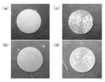
- Nitride coating formed Nitride coating formed, (c) Nitride coating of a comparative example formed on the surface of a substrate by microwave irradiation at 900 ° C. for 45 minutes by a conventional method using titanium powder, (d) It is an optical micrograph which shows the nitride coating of a comparative example formed on the back surface of a base material.
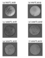
- the method for forming a nitride coating according to the embodiment of the present invention (a) 950 ° C., 30 minutes, (b) 950 ° C., 60 minutes, (c) 1000 ° C., 30 minutes, (d) 1000 ° C., 60 minutes.
- (E) 1050 ° C., 30 minutes, (f) 1050 ° C., 60 minutes, is an optical micrograph showing a nitride coating formed on the surface of the substrate by microwave irradiation.
- XRD X-ray diffraction
- FIG. 2 (a) A graph showing the surface roughness of the nitride coating formed on the surface of the base material by microwave irradiation at 900 ° C. for 45 minutes shown in FIG. 2 (a),
- FIG. 2 (b). 5 is a graph showing the surface roughness of the nitride coating of Comparative Example formed on the surface of the base material by microwave irradiation at 900 ° C. for 45 minutes shown in c).
- the method for forming a nitride coating according to the embodiment of the present invention which is a conventional method using a nitride coating (the present invention) formed on the surface of a substrate by microwave irradiation at 950 ° C. for 30 minutes, and titanium powder.
- the nitride coating of the comparative example (comparative example) formed on the surface of the base material by microwave irradiation at 950 ° C. for 30 minutes, and the titanium nitride formed on the surface of the base material by the ion plating method.
- FIG. 1 to 7 show a method of forming a nitride coating according to the embodiment of the present invention.
- a container 11 is filled with a powder containing particles made of nitride as a main component, and the powder thereof.
- the base material 13 is put in 12.
- the container 11 is a quartz tube silica wool 14 is laid on the bottom
- the powder 12 is a powder of titanium nitride (TiN, Ti 2 N, TiN x)
- the base material 13 is a disk-shaped Ti-6Al-4V alloy. Titanium nitride does not have a nitride forming ability.
- the entire container 11, that is, the base material 13 and the powder 12 around it is irradiated with microwaves.
- the surface of the base material 13 is coated with the nitride, and the nitride coating 15 can be formed.
- the frequency of the microwave to be irradiated is preferably 0.3 GHz to 30 GHz, more preferably 0.9 GHz to 30 GHz, and even more preferably 1 GHz to 5 GHz. Further, it is preferable to heat the base material 13 and the powder 12 around the base material 13 to 600 ° C. to 1300 ° C. by irradiation with microwaves.
- nitride placed in the container 11 is not limited to titanium nitride (TiN, Ti 2 N, TiN x), for example, lithium nitride (Li 3 N), yttrium nitride (YN), zirconium nitride (ZrN), hafnium nitride (HfN, etc.), Yttrium Nitride (VN, etc.), Niobide Nitride (NbN), Tantalum Nitride (TaN, etc.), Chromium Nitride (CrN, Cr 2 N), Molybdenum Nitride (MoN, Mo 2 N), Titanium Nitride (WN) , Titanium Nitride (W 2 N), Manganese Nitride (Mn 2 N, Mn 3 N 2 , Mn 4 N, etc.), Iron Nitride (Fe N, Fe 2 N, Fe 3 N, Fe 4 N, Fe 16 N 2 ), Titanium Nitride (CoN, Co 2
- the base material 13 is not limited to the titanium alloy, and for example, iron (Fe), cobalt (Co), nickel (Ni), copper (Cu), silver (Ag), gold (Au), zinc (Zn), and the like.
- Metals made of alloys silica (SiO 2 ), alumina (Al 2 O 3 ), tria (ThO 2 ), magnesia (MgO), itria (Y 2 O 3 ), zirconia (ZrO 2 ), zinc oxide (ZnO) Oxides such as silicon carbide (SiC), boron carbide (B 4 C), titanium carbide (TiC), chromium carbide (Cr 4 C 3 ), tantalum carbide (TaC), vanadium carbide (VC), zirconium carbide ( Ceramics containing carbides such as ZrC) and tungsten carbide (WC), nitrides, borides, calides, non-oxides such as carbon and the like may be used.
- the method for forming the nitride coating according to the embodiment of the present invention is only required to put the base material 13 in the powder 12 containing particles made of nitride as a main component and irradiate the base material with microwaves, and also in the atmosphere. It can be carried out at. Therefore, it is not necessary to adjust the pressure or replace the atmosphere, and the nitride coating 15 can be formed on the surface of the base material 13 by a simple process and a simple operation. Further, in the method for forming a nitride coating according to the embodiment of the present invention, the nitride can be uniformly coated by using particles made of nitride.
- the thickness of the nitride coating 15 can be increased by lengthening the microwave irradiation time, and the thickness of the nitride coating 15 can be increased by the microwave irradiation time. Can be adjusted. Further, the particles composed of the nitride remaining after the coating is formed can be reused when coating another substrate, which is efficient. Further, since it is not necessary to use the nitride particles and form the nitride by microwave irradiation, the microwave irradiation condition can be relaxed.
- the nitride coating 15 was formed on the surface of the base material 13 by using the method for forming the nitride coating according to the embodiment of the present invention shown in FIG.
- a quartz tube having an outer diameter of 23 mm and an inner diameter of 20 mm is filled in the container 11.
- TiN titanium nitride
- a Ti-6Al-4V alloy was used as a base material 13 and the outer diameter is 14.5 mm and the thickness is 1 mm.
- a Ti-6Al-4V alloy was used.
- a magnetron-type multimode microwave irradiation device was used to irradiate 2.45 GHz microwaves. Further, during the irradiation with microwaves, the temperature of the upper surface of the powder 12 filled in the container 11 was measured with a radiation thermometer.
- microwaves were irradiated so that the temperature measured by the radiation thermometer was constant at a predetermined temperature for a predetermined time.
- the temperature measured at the time of microwave irradiation and the time for maintaining the temperature were set to 900 ° C., 950 ° C., 1000 ° C. and 1050 ° C., and 30 minutes, 45 minutes and 60 minutes, respectively.
- titanium (Ti) powder particle size 45 ⁇ m or less, manufactured by High Purity Chemical Co., Ltd.
- the other nitrides are subjected to the same conditions. A coating was formed.
- FIG. 2 shows optical micrographs of the nitride coating on the front surface and the back surface of the sample formed by microwave irradiation at 900 ° C. for 45 minutes using titanium nitride powder and titanium powder (comparative example), respectively.
- FIG. 3 shows optical micrographs of the nitride coating on the sample surface formed by microwave irradiation at 950 ° C., 1000 ° C., and 1050 ° C. for 30 minutes and 60 minutes, respectively, using titanium nitride powder. ..
- the nitride coating of the comparative example formed using the titanium powder had uneven surfaces.
- the nitride coating formed by using the titanium nitride powder has a uniform surface and almost no unevenness, and is compared with the one using the titanium powder. It was confirmed that the nitride was uniformly coated. It was also confirmed that the nitride coating formed using the titanium nitride powder had a beautiful appearance and a good appearance, and the film thickness of the nitride coating was thinner than that using the titanium powder. ..
- the nitride is uniformly coated even when the temperature and time during microwave irradiation are 950 ° C to 1050 ° C and 30 minutes to 60 minutes. confirmed.
- the nitride coating increased as the temperature during microwave irradiation increased and as the microwave irradiation time increased.
- the surface of the sample on which the nitride coating was formed at 900 ° C. and 45 minutes shown in FIGS. 2 (a) and 2 (c) was measured by an X-ray diffraction method and the surface roughness was measured. went.
- the measurement result of X-ray diffraction is shown in FIG. 4, and the measurement result of surface roughness (Roughness) is shown in FIG.
- the nitride coating of the comparative example formed by using the titanium powder has the peak of TiN x as the main phase and uses the titanium nitride powder shown in FIG. 4 (a). It was confirmed that the peak of TiN was smaller than that of the above. From this, it can be said that the nitriding of the coated titanium powder has not sufficiently progressed in the comparative example.
- FIG. 6 also shows the measurement results of the Vickers hardness of the base material for comparison. As shown in FIG. 6, it was confirmed that the Vickers hardness was increased by forming the nitride coating and was larger than 600 HV.
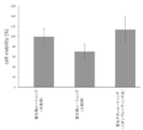
- a cell experiment was conducted on a sample in which a nitride coating was formed at 950 ° C. for 30 minutes.
- 1.0 ⁇ 10 4 rat gingival-derived cells were seeded on the surface of each sample, and 72 hours later, a reagent was added to each sample to develop color of living cells, and the absorbance was measured. The viable cell rate was calculated. Absorbance was measured 5 times for each sample, and the average value and standard deviation of the viable cell rate were calculated.
- the nitride coating formed by using the titanium nitride powder has an average viable cell rate of 99.5%, and the titanium nitride coating by the ion plating method (average viable cell rate). : 113.7%), but superior to the one using titanium powder (average viable cell rate: 70.2%), and it was confirmed that the viable cell rate was almost the same as that of pure titanium. .. From this result, it is considered that the nitride coating formed by using the titanium nitride powder can be used as a coating for, for example, a dental implant member, etc., instead of pure titanium or the like.
Landscapes
- Chemical & Material Sciences (AREA)
- Organic Chemistry (AREA)
- Inorganic Chemistry (AREA)
- Metallurgy (AREA)
- Engineering & Computer Science (AREA)
- Materials Engineering (AREA)
- Crystallography & Structural Chemistry (AREA)
- Mechanical Engineering (AREA)
- Physics & Mathematics (AREA)
- Thermal Sciences (AREA)
- Chemical Kinetics & Catalysis (AREA)
- Physical Vapour Deposition (AREA)
- Other Surface Treatments For Metallic Materials (AREA)
- Ceramic Products (AREA)
Abstract
【課題】簡単な工程かつ容易な操作で、窒化物をより均一にコーティングすることができる窒化物コーティングの形成方法を提供する。 【解決手段】窒化物から成る粒子を主成分として含む粉末12の中に基材13を入れ、その基材13およびその周囲の粉末12にマイクロ波を照射することにより、基材13の表面に窒化物をコーティングして、窒化物コーティング15を形成する。マイクロ波は、周波数が0.3GHz乃至30GHzであることが好ましい。また、マイクロ波を照射することにより、基材13およびその周囲の粉末12を、600℃乃至1300℃に加熱することが好ましい。
Description
本発明は、窒化物コーティングの形成方法に関する。
従来、窒化物コーティングの形成方法として、チタンまたはチタン基合金の表面に、CVD法(化学的蒸着)やPVD法(物理的蒸着)、プラズマCVD法、レーザーCVD法、イオン注入法等を用いて、窒化物被膜層を被覆して生体用インプラント部材を製造する方法(例えば、特許文献1参照)や、純チタンから成る基材の表面に、イオンプレーティング法により10~300℃の温度域で、窒化チタン層を形成して歯科用インプラント部材を製造する方法(例えば、特許文献2参照)がある。
しかし、特許文献1および2に記載の方法では、真空装備による圧力調整や雰囲気置換を行う必要があるため、製造工程が複雑になり、作業が効率的とはいえないという問題があった。そこで、この問題を解決するために、本発明者等により、大気中で実施可能な窒化物コーティング方法が開発されている(例えば、特許文献3参照)。この窒化物コーティング方法は、大気中において、基材を、窒化物形成能を有する物質の粉末中に入れ、マイクロ波を照射して交番電界中に曝すことにより、窒化物形成能を有する物質粉末が大気中の窒素成分と反応して生成される窒化物を、基材表面にコーティングするものである。
特許文献3に記載の窒化物コーティング方法によれば、簡単な工程かつ容易な操作で、基材の表面に窒化物をコーティングすることができるが、コーティングにややムラが生じていた。そこで、近年では、窒化物をより均一にコーティングする技術の開発が期待されていた。
本発明は、このような課題に着目してなされたもので、簡単な工程かつ容易な操作で、窒化物をより均一にコーティングすることができる窒化物コーティングの形成方法を提供することを目的とする。
特許文献3に記載の方法では、窒化チタン等の窒化物の合成には時間がかかることから(特許文献3の「0005」段落参照)、窒化物形成能を有する物質粉末が基材表面にコーティングされた後、その物質が窒化して、窒化物コーティングが形成されている。そこで、上記目的を達成するために、本発明者等は、コーティング過程と窒化過程とを入れ換え、既に窒化物として存在しているものを、マイクロ波を利用してコーティングすれば良いのではないかと考えて、本発明に至った。
すなわち、本発明に係る窒化物コーティングの形成方法は、窒化物から成る粒子を主成分として含む粉末中に基材を入れ、前記基材およびその周囲の前記粉末にマイクロ波を照射することにより、前記基材の表面に前記窒化物をコーティングすることを特徴とする。
本発明に係る窒化物コーティングの形成方法は、窒化物から成る粒子を主成分として含む粉末中に基材を入れて、マイクロ波を照射するだけでよく、また、大気中で実施可能である。このため、圧力調整や雰囲気置換を行う必要がなく、簡単な工程かつ容易な操作で、基材の表面に窒化物コーティングを形成することができる。また、本発明に係る窒化物コーティングの形成方法は、窒化物から成る粒子を使用することにより、窒化物形成能を有する物質の粉末を利用する特許文献3に記載の従来の方法と比べて、窒化物をより均一にコーティングすることができる。
本発明に係る窒化物コーティングの形成方法は、マイクロ波の照射時間を長くすると、窒化物コーティングの厚みを大きくすることができ、マイクロ波の照射時間により、窒化物コーティングの厚みを調整することができる。また、コーティング形成後に残った窒化物から成る粒子を、別の基材をコーティングする際に再利用することができ、効率的である。また、窒化物の粒子を使用し、マイクロ波の照射により窒化物を形成する必要がないため、マイクロ波照射条件を緩和することができる。なお、本発明に係る窒化物コーティングの形成方法で、基材を入れる粉末は、窒化物から成る粒子が主成分であり、窒化物から成る粒子を最も多く含んでいればよく、その粒子以外にも、酸化物の粒子など、他の粒子が入っていてもよいが、窒化物形成能を有さない粒子のみから成ることが好ましい。
本発明に係る窒化物コーティングの形成方法で、前記マイクロ波は、周波数が0.3GHz乃至30GHzであることが好ましく、0.9GHz以上であることがより好ましく、1GHz乃至5GHzであることがさらに好ましい。これらの場合、窒化物をより均一にコーティングすることができる。
本発明に係る窒化物コーティングの形成方法で、窒化物は、コーティングを形成可能なものであれば、いかなるものであってもよく、例えば、窒化チタン(TiN、Ti2N、TiNx)に限らず、例えば、窒化リチウム(Li3N)、窒化イットリウム(YN)、窒化ジルコニウム(ZrN)、窒化ハフニウム(HfNなど)、窒化バナジウム(VNなど)、窒化ニオブ(NbN)、窒化タンタル(TaNなど)、窒化クロム(CrN、Cr2N)、窒化モリブデン(MoN、Mo2N)、窒化タングステン(WN)、窒化タングステン(W2N)、窒化マンガン(Mn2N、Mn3N2、Mn4Nなど)、窒化鉄(FeN、Fe2N、Fe3N、Fe4N、Fe16N2)、窒化コバルト(CoN、Co2N、Co3N、Co4Nなど)、窒化ニッケル(Ni2N、Ni3N、Ni4N)、窒化銅(Cu3N)、窒化ホウ素(BN)、窒化アルミニウム(AlN)、窒化ガリウム(GaN)、窒化インジウム(InN)、窒化ケイ素(Si3N4)、窒化インジウムガリウム(InGaN)、窒化アルミニウムガリウム(AlGaN)、窒化アルミニウムインジウム(AlInN)、窒化インジウムガリウム(InGaN)、窒化チタンアルミニウム(TiAlN)、サイアロン(SiAlON)、酸窒化タンタルバリウム(BaTaO2N)、およびチタニウムカーボナイトライド(TiCN)のうちの少なくとも1種類、または、これらのうちの複数種類から成っていてもよい。これらの窒化物から形成される本発明に係る窒化物コーティングでは、例えば、窒化チタンコーティングは、黄金色で、鏡面仕上げの超硬質皮膜であり、導電性を有し、高強度、高靭性で耐衝撃性、耐熱衝撃性、耐摩耗性、耐食性に優れている。また、窒化ジルコニウム、窒化ニオブ、窒化タンタルなどのコーティングは、高強度、高靭性で耐衝撃性、耐摩耗性、耐食性に優れ、独特の電気的な特性や磁気的な特性、さらには光学的に有利な性状を有している。窒化アルミニウムコーティングは、空気中の加熱により酸化膜が形成されるため、酸化の進行を抑制する効果を有しており、さらに高い熱伝導性を有し、耐熱性、耐食性に優れている。窒化ケイ素コーティングは、電気的に絶縁性であり、高強度、高靭性で耐衝撃性、耐熱衝撃性、耐摩耗性、耐食性に優れている。
本発明に係る窒化物コーティングの形成方法で、基材は、マイクロ波の照射により溶解しないものであれば、いかなるものであってもよく、例えば、金属やセラミックスから成っていてもよい。金属から成る基材としては、例えば、鉄(Fe)、コバルト(Co)、ニッケル(Ni)、銅(Cu)、銀(Ag)、金(Au)、亜鉛(Zn)、アルミニウム(Al)、スズ(Sn)、チタン(Ti)、バナジウム(V)、クロム(Cr)、モリブデン(Mo)、マンガン(Mn)、タングステン(W)、白金(Pt)、鉛(Pb)、または、これらを含む合金から成るものである。セラミックスから成る基材としては、例えば、シリカ(SiO2)、アルミナ(Al2O3)、トリア(ThO2)、マグネシア(MgO)、イットリア(Y2O3)、ジルコニア(ZrO2)、酸化亜鉛(ZnO)等の酸化物や、炭化ケイ素(SiC)、炭化ホウ素(B4C)、炭化チタン(TiC)、炭化クロム(Cr4C3)、炭化タンタル(TaC)、炭化バナジウム(VC)、炭化ジルコニウム(ZrC)、炭化タングステン(WC)などの炭化物、窒化物、ホウ化物、ケイ化物、炭素等の非酸化物等を含むものである。
また、セラミックスの基材の表面に、本発明に係る窒化物コーティングの形成方法により窒化物コーティングが形成されたものは、例えば、磁性材料、磁気光学材料、超伝導体、導電材料、半導体、誘電体材料、圧電体材料、絶縁材料、基板、パッケージ、電気光学材料、固体レーザー発光材料、電子放射材料、切削・研磨材料、ドリル、刃物、磁器、ニューガラス、人工関節、人工骨、人工歯、工作機械部品、エンジン材料・動力機械部品、断熱材料などの電子工業材料、光学材料、工業材料、構造材料、生体関連材料、機能性セラミックス等として使用することができる。
本発明に係る窒化物コーティングの形成方法は、前記マイクロ波を照射することにより、前記基材およびその周囲の前記粉末を、600℃乃至1300℃に加熱することが好ましい。この場合、窒化物をより均一にコーティングすることができる。なお、窒化物の種類に応じて加熱温度は変化し、例えば、窒化物が窒化チタン(TiN)から成る場合には、マイクロ波の照射により、基材およびその周囲の粉末を、850℃乃至1100℃に加熱することが好ましい。
本発明によれば、簡単な工程かつ容易な操作で、窒化物をより均一にコーティングすることができる窒化物コーティングの形成方法を提供することができる。
以下、図面および実施例に基づいて、本発明の実施の形態について説明する。
図1乃至図7は、本発明の実施の形態の窒化物コーティングの形成方法を示している。
図1乃至図7は、本発明の実施の形態の窒化物コーティングの形成方法を示している。
本発明の実施の形態の窒化物コーティングの形成方法は、まず、図1(a)に示すように、容器11の中に、窒化物から成る粒子を主成分として含む粉末を充填し、その粉末12の中に基材13を入れる。図1(a)に示す具体的な一例では、容器11は、底部にシリカウール14が敷かれた石英管であり、粉末12は窒化チタン(TiN、Ti2N、TiNx)の粉末であり、基材13は、円板状のTi-6Al-4V合金である。なお、窒化チタンは、窒化物形成能を有していない。
次に、容器11の全体、すなわち基材13およびその周囲の粉末12に、マイクロ波を照射する。これにより、図1(b)に示すように、基材13の表面に窒化物がコーティングされ、窒化物コーティング15を形成することができる。なお、照射するマイクロ波は、周波数が0.3GHz乃至30GHzであることが好ましく、0.9GHz乃至30GHzであることがより好ましく、1GHz乃至5GHzであることがさらに好ましい。また、マイクロ波の照射により、基材13およびその周囲の粉末12を、600℃乃至1300℃に加熱することが好ましい。
なお、容器11に入れる窒化物は、窒化チタン(TiN、Ti2N、TiNx)に限らず、例えば、窒化リチウム(Li3N)、窒化イットリウム(YN)、窒化ジルコニウム(ZrN)、窒化ハフニウム(HfNなど)、窒化バナジウム(VNなど)、窒化ニオブ(NbN)、窒化タンタル(TaNなど)、窒化クロム(CrN、Cr2N)、窒化モリブデン(MoN、Mo2N)、窒化タングステン(WN)、窒化タングステン(W2N)、窒化マンガン(Mn2N、Mn3N2、Mn4Nなど)、窒化鉄(FeN、Fe2N、Fe3N、Fe4N、Fe16N2)、窒化コバルト(CoN、Co2N、Co3N、Co4Nなど)、窒化ニッケル(Ni2N、Ni3N、Ni4N)、窒化銅(Cu3N)、窒化ホウ素(BN)、窒化アルミニウム(AlN)、窒化ガリウム(GaN)、窒化インジウム(InN)、窒化ケイ素(Si3N4)、窒化インジウムガリウム(InGaN)、窒化アルミニウムガリウム(AlGaN)、窒化アルミニウムインジウム(AlInN)、窒化インジウムガリウム(InGaN)、窒化チタンアルミニウム(TiAlN)、サイアロン(SiAlON)、酸窒化タンタルバリウム(BaTaO2N)、およびチタニウムカーボナイトライド(TiCN)のうちの少なくとも1種類、または、これらのうちの複数種類から成っていてもよい。また、容器11に充填する粉末12は、窒化物形成能を有さない粒子のみから成っていればよく、窒化物の粒子以外にも、酸化物の粒子など、他の粒子が入っていてもよい。
また、基材13は、チタン合金に限らず、例えば、鉄(Fe)、コバルト(Co)、ニッケル(Ni)、銅(Cu)、銀(Ag)、金(Au)、亜鉛(Zn)、アルミニウム(Al)、スズ(Sn)、バナジウム(V)、クロム(Cr)、モリブデン(Mo)、マンガン(Mn)、タングステン(W)、白金(Pt)、鉛(Pb)、または、これらを含む合金から成る金属や、シリカ(SiO2)、アルミナ(Al2O3)、トリア(ThO2)、マグネシア(MgO)、イットリア(Y2O3)、ジルコニア(ZrO2)、酸化亜鉛(ZnO)等の酸化物や、炭化ケイ素(SiC)、炭化ホウ素(B4C)、炭化チタン(TiC)、炭化クロム(Cr4C3)、炭化タンタル(TaC)、炭化バナジウム(VC)、炭化ジルコニウム(ZrC)、炭化タングステン(WC)などの炭化物、窒化物、ホウ化物、ケイ化物、炭素等の非酸化物等を含むセラミックスであってもよい。
次に、作用について説明する。
本発明の実施の形態の窒化物コーティングの形成方法は、窒化物から成る粒子を主成分として含む粉末12の中に基材13を入れて、マイクロ波を照射するだけでよく、また、大気中で実施可能である。このため、圧力調整や雰囲気置換を行う必要がなく、簡単な工程かつ容易な操作で、基材13の表面に窒化物コーティング15を形成することができる。また、本発明の実施の形態の窒化物コーティングの形成方法は、窒化物から成る粒子を使用することにより、窒化物を均一にコーティングすることができる。
本発明の実施の形態の窒化物コーティングの形成方法は、窒化物から成る粒子を主成分として含む粉末12の中に基材13を入れて、マイクロ波を照射するだけでよく、また、大気中で実施可能である。このため、圧力調整や雰囲気置換を行う必要がなく、簡単な工程かつ容易な操作で、基材13の表面に窒化物コーティング15を形成することができる。また、本発明の実施の形態の窒化物コーティングの形成方法は、窒化物から成る粒子を使用することにより、窒化物を均一にコーティングすることができる。
本発明の実施の形態の窒化物コーティングの形成方法は、マイクロ波の照射時間を長くすると、窒化物コーティング15の厚みを大きくすることができ、マイクロ波の照射時間により、窒化物コーティング15の厚みを調整することができる。また、コーティング形成後に残った窒化物から成る粒子を、別の基材をコーティングする際に再利用することができ、効率的である。また、窒化物の粒子を使用し、マイクロ波の照射により窒化物を形成する必要がないため、マイクロ波照射条件を緩和することができる。
図1に示す本発明の実施の形態の窒化物コーティングの形成方法を利用して、基材13の表面に窒化物コーティング15を形成した。容器11として、外径23mm、内径20mmの石英管を、容器11に充填する粉末12として、窒化チタン(TiN)粉末を、基材13として、外径14.5mm、厚み1mmの円板状のTi-6Al-4V合金を使用した。また、マグネトロン式のマルチモード型マイクロ波照射装置を用いて、2.45GHzのマイクロ波を照射した。また、マイクロ波を照射中は、放射温度計により、容器11に充填した粉末12の上部表面の温度を計測した。
窒化物コーティング15の形成時には、放射温度計で計測される温度が、所定の温度で所定の時間一定となるように、マイクロ波を照射した。ここでは、マイクロ波照射時に計測される温度、ならびに、その温度を維持する時間を、それぞれ、900℃、950℃、1000℃および1050℃、ならびに、30分、45分および60分とした。また、比較例として、特許文献3の窒化物コーティング法に従って、容器に充填する粉末としてチタン(Ti)粉末(粒径45μm以下、高純度化学社製)を使用し、他は同じ条件で窒化物コーティングの形成を行った。
窒化チタン粉末およびチタン粉末(比較例)を用いて、それぞれ900℃で45分のマイクロ波照射により形成された試料の表面および裏面の窒化物コーティングの光学顕微鏡写真を、図2に示す。また、窒化チタン粉末を用いて、950℃、1000℃、1050℃で、それぞれ30分、60分のマイクロ波照射により形成された、試料表面の窒化物コーティングの光学顕微鏡写真を、図3に示す。
図2(c)および(d)に示すように、チタン粉末を用いて形成された比較例の窒化物コーティングは、表面にムラがあることが確認された。これに対し、図2(a)および(b)に示すように、窒化チタン粉末を用いて形成された窒化物コーティングは、表面が一様でムラがほとんどなく、チタン粉末を用いたものと比べて、均一に窒化物がコーティングされていることが確認された。また、窒化チタン粉末を用いて形成された窒化物コーティングは、外観がきれいで見た目もよく、チタン粉末を用いたものと比べて、窒化物コーティングの膜厚が薄くなっていることも確認された。
また、図3に示すように、マイクロ波照射時の温度および時間が、950℃~1050℃、及び、30分~60分のときであっても、均一に窒化物がコーティングされていることが確認された。図3(a)に示す950℃で30分のときには、やや表面に凹凸が認められるが、比較例の図2(c)および(d)と比べると、均一であるといえる。また、マイクロ波照射時の温度が高くなるに従って、また、マイクロ波照射時間が長くなるに従って、窒化物コーティングの膜厚が厚くなることも確認された。
次に、図2(a)および(c)に示す、900℃、45分で窒化物コーティングが形成された試料の表面に対して、X線回折法による測定、および、表面粗さの測定を行った。X線回折の測定結果を図4に、表面粗さ(Roughness)の測定結果を図5に示す。図4(b)に示すように、チタン粉末を用いて形成された比較例の窒化物コーティングは、TiNxのピークが主相であり、図4(a)に示す窒化チタン粉末を用いたものと比べ、TiNのピークが小さくなっていることが確認された。このことから、比較例では、コーティングされたチタン粉末の窒化が十分に進行していないといえる。
図5に示すように、窒化チタン粉末を用いて形成された窒化物コーティングは、算術平均粗さRaが0.3μm、最大高さRz(表面の最も高い部分と最も深い部分との差)が1.9μmであり、チタン粉末を用いた比較例(Ra=0.5μm、Rz=5.0μm)と比べて、値が小さくなっており、表面粗さが小さいことが確認された。また、チタン粉末を用いた比較例では、鋭いピークが認められているのに対し、窒化チタン粉末を用いたものは、鋭いピークは認められず、なだらかな凹凸のみが認められており、表面が比較的均一であることが確認された。
次に、窒化チタン粉末を用いて、900℃、60分で窒化物コーティングを形成した試料の表面に対して、ビッカース硬さ(Vickers Hardness;HV)の測定を行った。その測定結果を、図6に示す。なお、図6には、比較のため、基材のビッカース硬さの測定結果も示している。図6に示すように、窒化物コーティングを形成することにより、ビッカース硬さが大きくなり、600HVよりも大きくなっていることが確認された。
次に、窒化チタン粉末およびチタン粉末(比較例)を用いて、950℃、30分で窒化物コーティングを形成した試料について、細胞実験を行った。実験では、各試料の表面に、ラット歯肉由来細胞を1.0×10⁴個播種し、72時間後に、各試料に試薬を添加して、生存している細胞を発色させ、吸光度を測定して生細胞率を算出した。各試料に対して吸光度の測定を5回行い、生細胞率の平均値および標準偏差を算出した。また、比較例として、純チタンのみから成る試料、および、イオンプレーティング法(特許文献2参照)により窒化チタンをコーティングした試料を作成し、それらの試料に対して同様の測定を行い、生細胞率を算出した。なお、各試料の生細胞率は、純チタンで測定された生細胞率の平均値を100%として、算出している。生細胞率(cell viability)の測定結果を、図7に示す。
図7に示すように、窒化チタン粉末を用いて形成された窒化物コーティングは、生細胞率の平均値が99.5%であり、イオンプレーティング法による窒化チタンコーティング(生細胞率の平均値:113.7%)よりやや劣るが、チタン粉末を用いたもの(生細胞率の平均値:70.2%)よりも優れ、純チタンとほぼ同等の生細胞率であることが確認された。この結果から、窒化チタン粉末を用いて形成された窒化物コーティングは、純チタン等の代わりに、例えば、歯科用インプラント部材等のコーティングとして使用することができると考えられる。
11 容器
12 粉末
13 基材
14 シリカウール
15 窒化物コーティング
12 粉末
13 基材
14 シリカウール
15 窒化物コーティング
Claims (5)
- 窒化物から成る粒子を主成分として含む粉末中に基材を入れ、前記基材およびその周囲の前記粉末にマイクロ波を照射することにより、前記基材の表面に前記窒化物をコーティングすることを特徴とする窒化物コーティングの形成方法。
- 前記マイクロ波は、周波数が0.3GHz乃至30GHzであることを特徴とする請求項1記載の窒化物コーティングの形成方法。
- 前記マイクロ波を照射することにより、前記基材およびその周囲の前記粉末を、600℃乃至1300℃に加熱することを特徴とする請求項1または2記載の窒化物コーティングの形成方法。
- 前記窒化物は窒化チタン(TiN)から成り、前記マイクロ波を照射することにより、前記基材およびその周囲の前記粉末を、850℃乃至1100℃に加熱することを特徴とする請求項1または2記載の窒化物コーティングの形成方法。
- 前記粉末は、窒化物形成能を有さない粒子のみから成ることを特徴とする請求項1乃至4のいずれか1項に記載の窒化物コーティングの形成方法。
Priority Applications (1)
| Application Number | Priority Date | Filing Date | Title |
|---|---|---|---|
| JP2021504911A JP7448157B2 (ja) | 2019-03-14 | 2020-02-27 | 窒化物コーティングの形成方法 |
Applications Claiming Priority (2)
| Application Number | Priority Date | Filing Date | Title |
|---|---|---|---|
| JP2019-047471 | 2019-03-14 | ||
| JP2019047471 | 2019-03-14 |
Publications (1)
| Publication Number | Publication Date |
|---|---|
| WO2020184192A1 true WO2020184192A1 (ja) | 2020-09-17 |
Family
ID=72426553
Family Applications (1)
| Application Number | Title | Priority Date | Filing Date |
|---|---|---|---|
| PCT/JP2020/007900 Ceased WO2020184192A1 (ja) | 2019-03-14 | 2020-02-27 | 窒化物コーティングの形成方法 |
Country Status (2)
| Country | Link |
|---|---|
| JP (1) | JP7448157B2 (ja) |
| WO (1) | WO2020184192A1 (ja) |
Cited By (2)
| Publication number | Priority date | Publication date | Assignee | Title |
|---|---|---|---|---|
| CN116497314A (zh) * | 2023-03-23 | 2023-07-28 | 南京航空航天大学 | 一种钛合金表面耐磨抗氧化四元氮化物涂层及其制备方法与应用 |
| CN117179569A (zh) * | 2023-08-09 | 2023-12-08 | 九阳股份有限公司 | 锅具及锅具制造方法 |
Citations (3)
| Publication number | Priority date | Publication date | Assignee | Title |
|---|---|---|---|---|
| JPH10212168A (ja) * | 1997-01-29 | 1998-08-11 | Kyocera Corp | セラミック加熱装置 |
| JP2007084896A (ja) * | 2005-09-26 | 2007-04-05 | Tohoku Univ | 窒化物コーティング法 |
| JP2007223137A (ja) * | 2006-02-23 | 2007-09-06 | National Institute Of Advanced Industrial & Technology | マイクロ波加熱用鋳込み型及びセラミックス焼結体の製造方法 |
Family Cites Families (1)
| Publication number | Priority date | Publication date | Assignee | Title |
|---|---|---|---|---|
| JP5058672B2 (ja) | 2007-05-14 | 2012-10-24 | 新日本製鐵株式会社 | 金属表面皮膜の封孔処理方法、および金属表面皮膜の封孔処理装置 |
-
2020
- 2020-02-27 WO PCT/JP2020/007900 patent/WO2020184192A1/ja not_active Ceased
- 2020-02-27 JP JP2021504911A patent/JP7448157B2/ja active Active
Patent Citations (3)
| Publication number | Priority date | Publication date | Assignee | Title |
|---|---|---|---|---|
| JPH10212168A (ja) * | 1997-01-29 | 1998-08-11 | Kyocera Corp | セラミック加熱装置 |
| JP2007084896A (ja) * | 2005-09-26 | 2007-04-05 | Tohoku Univ | 窒化物コーティング法 |
| JP2007223137A (ja) * | 2006-02-23 | 2007-09-06 | National Institute Of Advanced Industrial & Technology | マイクロ波加熱用鋳込み型及びセラミックス焼結体の製造方法 |
Cited By (2)
| Publication number | Priority date | Publication date | Assignee | Title |
|---|---|---|---|---|
| CN116497314A (zh) * | 2023-03-23 | 2023-07-28 | 南京航空航天大学 | 一种钛合金表面耐磨抗氧化四元氮化物涂层及其制备方法与应用 |
| CN117179569A (zh) * | 2023-08-09 | 2023-12-08 | 九阳股份有限公司 | 锅具及锅具制造方法 |
Also Published As
| Publication number | Publication date |
|---|---|
| JPWO2020184192A1 (ja) | 2020-09-17 |
| JP7448157B2 (ja) | 2024-03-12 |
Similar Documents
| Publication | Publication Date | Title |
|---|---|---|
| CN106102972B (zh) | 被覆切削工具和其制造方法 | |
| JP3866305B2 (ja) | 工具用複合高硬度材料 | |
| JP7112330B2 (ja) | 基材上に硬質材料層を製造するための方法、硬質材料層、切削工具及び被膜源 | |
| JP3384110B2 (ja) | 被覆切削工具とその製造方法 | |
| JP4765069B2 (ja) | 窒化物コーティング法 | |
| CN101960051A (zh) | 用于切削刀具刀片的热稳定(Ti,Si)N层 | |
| CN107636193A (zh) | 涂层切削刀具和对所述切削刀具进行涂覆的方法 | |
| JP3249277B2 (ja) | 耐摩耗性被覆部材 | |
| JP7448157B2 (ja) | 窒化物コーティングの形成方法 | |
| US20070111032A1 (en) | Surface-coated article, production method therefor, machine tool, and machine tool apparatus | |
| JP2013096004A (ja) | 耐剥離性に優れる被覆工具およびその製造方法 | |
| EP1666413B1 (en) | Tantalum carbide, method for producing tantalum carbide, tantalum carbide wiring and tantalum carbide electrode | |
| WO2004108338A1 (ja) | 加工機用ノズル、溶接用コンタクトチップ、加工機用ノズルの製造方法、溶接用コンタクトチップの製造方法 | |
| KR20170118872A (ko) | 피복절삭공구 | |
| JPS60208473A (ja) | 人工ダイヤモンド被覆工具部材 | |
| JP2005297141A (ja) | 表面被覆スローアウェイチップ | |
| EP1746178A3 (en) | Device for improving plasma activity in PVD-reactors | |
| JP2012228735A (ja) | 耐摩耗性に優れる被覆工具およびその製造方法 | |
| JP2015139863A (ja) | 高速断続切削加工においてすぐれた耐チッピング性を発揮する表面被覆切削工具 | |
| JP2016078137A (ja) | 超硬工具 | |
| JP5035979B2 (ja) | 高速ミーリング加工で硬質被覆層がすぐれた耐摩耗性を発揮する表面被覆切削工具およびその製造方法 | |
| JP2004338041A (ja) | 切削インサート及び工具ユニット | |
| KR20200007861A (ko) | 고온 부품 | |
| JP2017166011A (ja) | 被膜、切削工具および被膜の製造方法 | |
| JP4815925B2 (ja) | 被覆焼結合金 |
Legal Events
| Date | Code | Title | Description |
|---|---|---|---|
| 121 | Ep: the epo has been informed by wipo that ep was designated in this application |
Ref document number: 20770069 Country of ref document: EP Kind code of ref document: A1 |
|
| ENP | Entry into the national phase |
Ref document number: 2021504911 Country of ref document: JP Kind code of ref document: A |
|
| NENP | Non-entry into the national phase |
Ref country code: DE |
|
| 122 | Ep: pct application non-entry in european phase |
Ref document number: 20770069 Country of ref document: EP Kind code of ref document: A1 |