WO2020183989A1 - インダクタ - Google Patents
インダクタ Download PDFInfo
- Publication number
- WO2020183989A1 WO2020183989A1 PCT/JP2020/004223 JP2020004223W WO2020183989A1 WO 2020183989 A1 WO2020183989 A1 WO 2020183989A1 JP 2020004223 W JP2020004223 W JP 2020004223W WO 2020183989 A1 WO2020183989 A1 WO 2020183989A1
- Authority
- WO
- WIPO (PCT)
- Prior art keywords
- wiring
- region
- particles
- center
- wirings
- Prior art date
- Legal status (The legal status is an assumption and is not a legal conclusion. Google has not performed a legal analysis and makes no representation as to the accuracy of the status listed.)
- Ceased
Links
Images


Classifications
-
- H—ELECTRICITY
- H01—ELECTRIC ELEMENTS
- H01F—MAGNETS; INDUCTANCES; TRANSFORMERS; SELECTION OF MATERIALS FOR THEIR MAGNETIC PROPERTIES
- H01F17/00—Fixed inductances of the signal type
- H01F17/04—Fixed inductances of the signal type with magnetic core
-
- H—ELECTRICITY
- H01—ELECTRIC ELEMENTS
- H01F—MAGNETS; INDUCTANCES; TRANSFORMERS; SELECTION OF MATERIALS FOR THEIR MAGNETIC PROPERTIES
- H01F1/00—Magnets or magnetic bodies characterised by the magnetic materials therefor; Selection of materials for their magnetic properties
- H01F1/01—Magnets or magnetic bodies characterised by the magnetic materials therefor; Selection of materials for their magnetic properties of inorganic materials
- H01F1/03—Magnets or magnetic bodies characterised by the magnetic materials therefor; Selection of materials for their magnetic properties of inorganic materials characterised by their coercivity
- H01F1/12—Magnets or magnetic bodies characterised by the magnetic materials therefor; Selection of materials for their magnetic properties of inorganic materials characterised by their coercivity of soft-magnetic materials
- H01F1/14—Magnets or magnetic bodies characterised by the magnetic materials therefor; Selection of materials for their magnetic properties of inorganic materials characterised by their coercivity of soft-magnetic materials metals or alloys
- H01F1/20—Magnets or magnetic bodies characterised by the magnetic materials therefor; Selection of materials for their magnetic properties of inorganic materials characterised by their coercivity of soft-magnetic materials metals or alloys in the form of particles, e.g. powder
- H01F1/28—Magnets or magnetic bodies characterised by the magnetic materials therefor; Selection of materials for their magnetic properties of inorganic materials characterised by their coercivity of soft-magnetic materials metals or alloys in the form of particles, e.g. powder dispersed or suspended in a bonding agent
-
- H—ELECTRICITY
- H01—ELECTRIC ELEMENTS
- H01F—MAGNETS; INDUCTANCES; TRANSFORMERS; SELECTION OF MATERIALS FOR THEIR MAGNETIC PROPERTIES
- H01F27/00—Details of transformers or inductances, in general
- H01F27/34—Special means for preventing or reducing unwanted electric or magnetic effects, e.g. no-load losses, reactive currents, harmonics, oscillations, leakage fields
Definitions
- the present invention relates to an inductor.
- inductors are mounted on electronic devices and used as passive elements such as voltage conversion members.
- a rectangular parallelepiped chip body made of a magnetic material and an internal conductor such as copper embedded inside the chip body, and the cross-sectional shape of the chip body and the cross-sectional shape of the internal conductor are similar.
- An inductor has been proposed (see Patent Document 1). That is, in the inductor of Patent Document 1, a magnetic material is coated around a wiring (inner conductor) having a rectangular parallelepiped shape (rectangular parallelepiped shape).
- anisotropic magnetic particles such as flat magnetic particles as a magnetic material and to orient the anisotropic magnetic particles around the wiring to improve the inductance of the inductor. ..
- inductors with multiple wirings are also required.
- the magnetisms of the adjacent wires affect each other, causing a problem (crosstalk) in which noise is generated.
- the present invention provides an inductor that has good inductance and DC superimposition characteristics and can suppress crosstalk.
- the present invention [1] includes a plurality of wirings having a substantially circular shape in cross-sectional view and a magnetic layer covering the plurality of wirings, and the plurality of wirings are arranged at intervals from each other in the first direction.
- Each of the plurality of wirings includes a lead wire and an insulating layer covering the lead wire, the magnetic layer contains anisotropic magnetic particles and a binder, and the magnetic layer includes the plurality of wires.
- the peripheral region has a second region that is not provided, and the peripheral region advances the value 1.5 times the distance from the center of gravity of the wiring to the outer surface of the wiring to the outside from the outer surface of the wiring.
- An inductor that is a region and the center of the virtual arc connecting one end in the circumferential direction and the other end in the circumferential direction in the second region does not exist on the first virtual line passing through the centers of the plurality of wirings adjacent to each other. Including.
- the inductance is good because there is a first region around each of the plurality of wirings in which the anisotropic magnetic particles are oriented along the circumferential direction.
- the DC superimposition characteristic is good.
- the center in the second region does not exist on the first virtual line passing through the centers of the plurality of wirings adjacent to each other. Therefore, the distance that the magnetic flux reaches from one wiring to the other wiring via the second region can be increased. That is, the distance of the magnetic flux between the wirings can be substantially increased. Therefore, the influence of magnetism from one wiring to the other wiring can be reduced, and crosstalk can be suppressed.
- the center of the virtual arc is located between the first virtual line and the second virtual line passing through the center of the wiring and orthogonal to the first virtual line [1]. ] Is included.
- this inductor a plurality of wirings are arranged on one magnetic layer, and then the other magnetic layer is laminated on one magnetic layer so that the plurality of wirings are embedded in the second region.
- An inductor whose center is located between the first virtual line and the second virtual line can be manufactured. Therefore, the inductor according to [1] can be easily manufactured.
- the inductance and DC superimposition characteristics are good, and crosstalk can be suppressed.
- FIG. 1A-B is an embodiment of the inductor of the present invention
- FIG. 1A is a plan view
- FIG. 1B is a sectional view taken along the line AA of FIG. 1A
- FIG. 2 shows a partially enlarged view of the broken line portion of FIG. 1B
- 3A-B show the inductor manufacturing process shown in FIGS. 1A-B
- FIG. 3A shows an arrangement process
- FIG. 3B shows a lamination process.
- FIG. 4 shows an actual SEM photographic sectional view of the inductor shown in FIGS. 1A-B.
- FIG. 5 shows a cross-sectional view of a modified example of the inductor of the present invention (a form in which the intersection is located at the lower end of the wiring).
- FIG. 6 shows a plan view of an inductor model used in the simulations of Examples and Comparative Examples.
- 7A-C are cross-sectional views taken along the line AA of FIG. 6,
- FIG. 7A shows a cross-sectional view of Example 1
- FIG. 7B is a cross-sectional view of Comparative Example 1
- FIG. 7C shows Comparative Example 2.
- the left-right direction of the paper surface is the first direction
- the left side of the paper surface is one side of the first direction
- the right side of the paper surface is the other side of the first direction.
- the vertical direction of the paper surface is the second direction (direction orthogonal to the first direction)
- the upper side of the paper surface is one side of the second direction (one direction in the wiring axis direction)
- the lower side of the paper surface is the other side of the second direction (the other direction of the wiring axis).
- the paper thickness direction is the vertical direction (third direction orthogonal to the first and second directions, thickness direction)
- the front side of the paper is the upper side (one side of the third direction, one side of the thickness direction)
- the back side of the paper is.
- the lower side (the other side in the third direction, the other side in the thickness direction). Specifically, it conforms to the direction arrows in each figure.
- the inductor 1 has a substantially rectangular shape in a plan view extending in the plane direction (first direction and second direction).
- the inductor 1 includes a plurality of (two) wirings 2 and a magnetic layer 3.
- Each of the plurality of wirings 2 includes a first wiring 4 and a second wiring 5 arranged at a distance from the first wiring 4 in the width direction (first direction).
- the first wiring 4 extends long in the second direction and has, for example, a substantially U-shape in a plan view. As shown in FIG. 2, the first wiring 4 has a substantially circular shape in cross section.
- the first wiring 4 includes a lead wire 6 and an insulating layer 7 that covers the lead wire 6.
- the lead wire 6 extends long in the second direction and has, for example, a substantially U-shape in a plan view. Further, the lead wire 6 has a substantially circular shape in cross section that shares the central axis with the first wiring 4.
- the material of the lead wire 6 is, for example, a metal conductor such as copper, silver, gold, aluminum, nickel, and an alloy thereof, and copper is preferable.
- the conducting wire 6 may have a single-layer structure, or may have a multi-layer structure in which the surface of a core conductor (for example, copper) is plated (for example, nickel).
- the radius R1 of the lead wire 6 is, for example, 25 ⁇ m or more, preferably 50 ⁇ m or more, and for example, 2000 ⁇ m or less, preferably 200 ⁇ m or less.
- the insulating layer 7 is a layer for protecting the lead wire 6 from chemicals and water and preventing a short circuit of the lead wire 6.
- the insulating layer 7 is arranged so as to cover the entire outer peripheral surface of the conducting wire 6.
- the insulating layer 7 has a substantially annular shape in cross section that shares the central axis (center C1) with the first wiring 4.
- Examples of the material of the insulating layer 7 include insulating resins such as polyvinylformal, polyester, polyesterimide, polyamide (including nylon), polyimide, polyamideimide, and polyurethane. These may be used alone or in combination of two or more.
- insulating resins such as polyvinylformal, polyester, polyesterimide, polyamide (including nylon), polyimide, polyamideimide, and polyurethane. These may be used alone or in combination of two or more.
- the insulating layer 7 may be composed of a single layer or may be composed of a plurality of layers.
- the thickness R2 of the insulating layer 7 is substantially uniform in the radial direction of the wiring 2 at any position in the circumferential direction, for example, 1 ⁇ m or more, preferably 3 ⁇ m or more, and for example, 100 ⁇ m or less, preferably 100 ⁇ m or less. , 50 ⁇ m or less.
- the ratio (R1 / R2) of the radius R1 of the lead wire 6 to the thickness R2 of the insulating layer 7 is, for example, 1 or more, preferably 10 or more, and for example, 200 or less, preferably 100 or less.
- the radius (R1 + R2) of the first wiring 4 is, for example, 25 ⁇ m or more, preferably 50 ⁇ m or more, and for example, 2000 ⁇ m or less, preferably 200 ⁇ m or less.
- the center-to-center distance D2 of the first wiring 4 is the same distance as the center-to-center distance D1 between a plurality of wirings 2 described later, and is, for example, 20 ⁇ m or more, preferably 20 ⁇ m or more. It is 50 ⁇ m or more, and is, for example, 3000 ⁇ m or less, preferably 2000 ⁇ m or less.
- the second wiring 5 has the same shape as the first wiring 4 and has the same configuration, dimensions, and materials. That is, the second wiring 5 includes a lead wire 6 and an insulating layer 7 covering the lead wire 6 as in the first wiring 4.
- the distance D1 between the centers of the first wiring 4 and the second wiring 5 is, for example, 20 ⁇ m or more, preferably 50 ⁇ m or more, and for example, 3000 ⁇ m or less, preferably 2000 ⁇ m or less.
- the magnetic layer 3 is a layer for improving the inductance.
- the magnetic layer 3 is arranged so as to cover the entire outer peripheral surface of the plurality of wirings 2.
- the magnetic layer 3 forms the outer shape of the inductor 1.
- the magnetic layer 3 has a substantially rectangular shape in a plan view extending in the plane direction (first direction and second direction). Further, the magnetic layer 3 exposes the second-direction end edges of the plurality of wirings 2 on the other surface in the second direction.
- the magnetic layer 3 is formed of a magnetic composition containing anisotropic magnetic particles 8 and a binder 9.
- Examples of the magnetic material constituting the anisotropic magnetic particle (hereinafter, also abbreviated as “particle”) 8 include a soft magnetic material and a hard magnetic material.
- a soft magnetic material is preferably used from the viewpoint of inductance.
- the soft magnetic material examples include a single metal body containing one kind of metal element in a pure substance state, for example, one or more kinds of metal elements (first metal element) and one or more kinds of metal elements (second metal element).
- first metal element one or more kinds of metal elements
- second metal element one or more kinds of metal elements
- the single metal body examples include a single metal composed of only one kind of metal element (first metal element).
- the first metal element is appropriately selected from, for example, iron (Fe), cobalt (Co), nickel (Ni), and other metal elements that can be contained as the first metal element of the soft magnetic material. ..
- the single metal body includes, for example, a core containing only one kind of metal element and a surface layer containing an inorganic substance and / or an organic substance that modifies a part or all of the surface of the core, for example.
- examples thereof include an organic metal compound containing a first metal element and a form in which an inorganic metal compound is decomposed (thermal decomposition, etc.).
- thermal decomposition etc.
- iron powder obtained by thermally decomposing an organic iron compound (specifically, carbonyl iron) containing iron as the first metal element (sometimes referred to as carbonyl iron powder). And so on.
- the position of the layer containing the inorganic substance and / or the organic substance that modifies the portion containing only one kind of metal element is not limited to the above-mentioned surface.
- the organometallic compound or inorganic metal compound capable of obtaining a single metal body is not particularly limited, and a known or commonly used organometallic compound or inorganic metal compound capable of obtaining a soft magnetic single metal body is not particularly limited. Can be appropriately selected from.
- the alloy body is a eutectic of one or more kinds of metal elements (first metal element) and one or more kinds of metal elements (second metal element) and / or non-metal elements (carbon, nitrogen, silicon, phosphorus, etc.). It is not particularly limited as long as it is a body and can be used as an alloy body of a soft magnetic material.
- the first metal element is an essential element in the alloy body, and examples thereof include iron (Fe), cobalt (Co), and nickel (Ni). If the first metal element is Fe, the alloy body is an Fe-based alloy, and if the first metal element is Co, the alloy body is a Co-based alloy, and the first metal element is Ni. For example, the alloy body is a Ni-based alloy.
- the second metal element is an element (sub-component) secondarily contained in the alloy body, and is a metal element that is compatible (cofusable) with the first metal element.
- iron (Fe) the first. 1 When the metal element is other than Fe), Cobalt (Co) (when the first metal element is other than Co), Nickel (Ni) (when the first metal element is other than Ni), Chromium (Cr), Aluminum (Al), Silicon (Si), Copper (Cu), Silver (Ag), Manganese (Mn), Calcium (Ca), Barium (Ba), Titanium (Ti), Zirconium (Zr), Hafnium (Hf), Vanadium (V), Niob (Nb), Tantal (Ta), Molybdenum (Mo), Tungsten (W), Ruthenium (Ru), Rodium (Rh), Zinc (Zn), Gallium (Ga), Indium (In), Examples thereof include germanium (Ge), tin (Sn), lead (Pb), scandium (Sc), a
- the non-metal element is an element (sub-component) secondarily contained in the alloy body, and is a non-metal element that is compatible (combined) with the first metal element.
- boron (B) and carbon examples thereof include (C), nitrogen (N), silicon (Si), phosphorus (P) and sulfur (S). These can be used alone or in combination of two or more.
- Fe-based alloys examples include magnetic stainless steel (Fe-Cr-Al-Si alloy) (including electromagnetic stainless steel), sentust (Fe-Si-Al alloy) (including super sentust), and permalloy (including supersendust).
- magnetic stainless steel Fe-Cr-Al-Si alloy
- sentust Fe-Si-Al alloy
- permalloy including supersendust
- Fe-Ni alloy Fe-Ni alloy
- Fe-Ni-Mo alloy Fe-Ni-Mo-Cu alloy
- Fe-Ni-Co alloy Fe-Cr alloy
- Fe-Cr-Al alloy Fe-Ni-Cr alloy
- Fe- Ni—Cr—Si alloy silicon copper (Fe—Cu—Si alloy)
- Fe—Si alloy Fe—Si—B (—Cu—Nb) alloy
- Fe—B—Si—Cr alloy Fe—Si—Cr -Ni alloy
- Fe-Si-Cr alloy Fe-Si-Al-Ni-Cr alloy
- Fe-Ni-Si-Co alloy Fe-N alloy, Fe-C alloy, Fe-B alloy, Fe-P alloy
- Ferrites stainless ferrites, Mn-Mg-based ferrites, Mn-Zn-based ferrites, Ni-Zn-based ferrites, Ni-Zn-Cu-based ferrites, Cu-Zn-based ferrites, Cu-Mg-Zn-based
- Co-based alloys examples include Co-Ta-Zr and cobalt (Co) -based amorphous alloys.
- Ni-based alloys which are examples of alloys, include Ni—Cr alloys.
- an alloy body is preferable, an Fe-based alloy is more preferable, and Sendust (Fe—Si—Al alloy) is more preferable, from the viewpoint of magnetic properties.
- the soft magnetic material preferably a single metal body, more preferably a single metal body containing an iron element in a pure substance state, still more preferably iron alone or iron powder (carbonyl iron powder). Can be mentioned.
- the shape of the particles 8 examples include a flat shape (plate shape) and a needle shape from the viewpoint of anisotropy, and preferably from the viewpoint of good relative magnetic permeability in the plane direction (two-dimensional). Flat shape is mentioned.
- the magnetic layer 3 may further contain non-anisotropic magnetic particles in addition to the anisotropic magnetic particles 8.
- the non-anisotropic magnetic particles may have a shape such as a spherical shape, a granular shape, a lump shape, or a pellet shape.
- the average particle size of the non-anisotropic magnetic particles is, for example, 0.1 ⁇ m or more, preferably 0.5 ⁇ m or more, and for example, 200 ⁇ m or less, preferably 150 ⁇ m or less.
- the flatness (flatness) of the flat particles 8 is, for example, 8 or more, preferably 15 or more, and for example, 500 or less, preferably 450 or less.
- the flatness is calculated as, for example, an aspect ratio obtained by dividing the average particle diameter (average length) (described later) of the particles 8 by the average thickness of the particles 8.
- the average particle diameter (average length) of the particles 8 is, for example, 3.5 ⁇ m or more, preferably 10 ⁇ m or more, and for example, 200 ⁇ m or less, preferably 150 ⁇ m or less. If the particles 8 are flat, their average thickness is, for example, 0.1 ⁇ m or more, preferably 0.2 ⁇ m or more, and for example, 3.0 ⁇ m or less, preferably 2.5 ⁇ m or less.
- binder 9 examples include a thermosetting resin and a thermoplastic resin.
- thermosetting resin examples include epoxy resin, phenol resin, melamine resin, thermosetting polyimide resin, unsaturated polyester resin, polyurethane resin, silicone resin and the like. From the viewpoint of adhesiveness, heat resistance and the like, epoxy resin and phenol resin are preferable.
- thermoplastic resin examples include acrylic resin, ethylene-vinyl acetate copolymer, polycarbonate resin, polyamide resin (6-nylon, 6,6-nylon, etc.), thermoplastic polyimide resin, saturated polyester resin (PET, PBT, etc.). ) And so on. Acrylic resin is preferable.
- the binder 9 includes a combination of a thermosetting resin and a thermoplastic resin. More preferably, the combined use of an acrylic resin, an epoxy resin and a phenol resin can be mentioned. As a result, the particles 8 can be more reliably fixed around the wiring 2 in a predetermined orientation state and with a high filling.
- the magnetic composition can also contain additives such as a thermosetting catalyst, inorganic particles, organic particles, and a cross-linking agent, if necessary.
- the particles 8 are uniformly arranged while being oriented in the binder 9.
- the magnetic layer 3 has a peripheral region 11 and an outer region 12 in a cross-sectional view.
- the peripheral region 11 is a peripheral region of the wiring 2, and is located around the plurality of wirings 2 so as to come into contact with the plurality of wirings 2.
- the peripheral region 11 has a substantially annular shape in cross section that shares the central axis with the wiring 2. More specifically, the peripheral region 11 is 1.5 times the radius of the wiring 2 (distance from the center (centroid) C1 of the wiring 2 to the outer peripheral surface; R1 + R2) of the magnetic layer 3 (preferably 1). .2 times value, more preferably 1 time value, further preferably 0.8 times value, particularly preferably 0.5 times value), a region extending radially outward from the outer peripheral surface of the wiring 2.
- the peripheral region 11 is arranged around each of the plurality of wirings 2, that is, around the first wiring 4 and the second wiring 5.
- the peripheral region 11 includes a plurality of (two) first regions 13 and a plurality of (two) second regions 14, respectively.
- the plurality of first regions 13 are circumferential orientation regions. That is, in the first region 13, the particles 8 are oriented along the circumferential direction of the wiring 2 (first wiring 4 or second wiring 5).
- the plurality of first regions 13 are arranged on the upper side (one side in the third direction) and the lower side (the other side in the third direction) of the wiring 2 so as to face each other with the center C1 of the wiring 2 interposed therebetween. That is, the plurality of first regions 13 include an upper first region 15 arranged on the upper side of the wiring 2 and a lower first region 16 arranged on the lower side of the wiring 2. Further, the center C1 of the wiring 2 is located at the center in the vertical direction of the upper first region 15 and the lower first region 16.
- the direction in which the relative magnetic permeability of the particles 8 is high is abbreviated as the tangent of a circle centered on the center C1 of the wiring 2.
- Match More specifically, when the angle formed by the plane direction of the particle 8 and the tangent line of the circle in which the particle 8 is located is 15 ° or less, it is defined that the particle 8 is oriented in the circumferential direction. ..
- the ratio of the number of particles 8 oriented in the circumferential direction to the total number of particles 8 contained in the first region 13 exceeds, for example, 50%, preferably 70% or more, and more preferably 70% or more. , 80% or more. That is, the first region 13 may contain particles 8 that are not oriented in the circumferential direction, for example, less than 50%, preferably 30% or less, and more preferably 20% or less.
- the total area ratio of the plurality of first regions 13 is, for example, 40% or more, preferably 50% or more, more preferably 60% or more, and for example, 90% or less with respect to the entire peripheral region 11. , Preferably 80% or less.
- the circumferential relative permeability of the first region 13 is, for example, 5 or more, preferably 10 or more, more preferably 30 or more, and for example, 500 or less.
- the radial relative magnetic permeability is, for example, 1 or more, preferably 5 or more, and for example, 100 or less, preferably 50 or less, more preferably 25 or less.
- the ratio of the relative magnetic permeability in the circumferential direction to the radial direction (circumferential direction / radial direction) is, for example, 2 or more, preferably 5 or more, and for example, 50 or less. If the relative magnetic permeability is in the above range, the inductance is excellent.
- the specific magnetic permeability can be measured by, for example, an impedance analyzer (manufactured by Agilent, “4291B”) using a magnetic material test fixture.
- the plurality of second regions 14 are circumferential non-oriented regions. That is, in the second region 14, the particles 8 are not oriented along the circumferential direction of the wiring 2. In other words, in the second region 14, the particles 8 are oriented or not oriented along a direction other than the circumferential direction of the wiring 2 (for example, the first direction or the radial direction).
- the plurality of second regions 14 are arranged on one side and the other side of the wiring 2 in the first direction so as to face each other with the wiring 2 interposed therebetween. That is, the plurality of second regions 14 are located on one side of the second region 17 of the wiring 2 (first wiring 4 or the second wiring 5) arranged on one side in the first direction and on the other side of the wiring 2 in the first direction. It has a second region 18 on the other side to be arranged.
- the second region 17 on one side and the second region 18 on the other side are substantially line-symmetrical with respect to the second virtual line L3.
- the second virtual line L3 is a straight line that passes through the center C1 of the first wiring 4 or the second wiring 5 and extends in the vertical direction.
- the direction in which the relative magnetic permeability of the particles 8 is high coincides with the tangent line of the circle centered on the center C1 of the wiring 2. do not do. More specifically, when the angle formed by the plane direction of the particle 8 and the tangent line of the circle in which the particle 8 is located exceeds 15 °, it is defined that the particle 8 is not oriented in the circumferential direction. ..
- the ratio of the number of particles 8 that are not oriented in the circumferential direction to the total number of particles 8 included in the second region 14 exceeds 50%, preferably 70% or more, and for example. , 95% or less, preferably 90% or less.
- the second region 14 may include, for example, particles 8 oriented in the circumferential direction.
- the ratio of the number of particles 8 oriented in the circumferential direction to the total number of particles 8 included in the second region 14 is less than 50%, preferably 30% or less, and for example, 5 % Or more, preferably 10% or more.
- the particles 8 oriented in the circumferential direction are included, the particles 8 oriented in the circumferential direction are preferably arranged on the innermost side of the second region 14, that is, on the surface of the wiring 2.
- the total area ratio of the plurality of second regions 14 is, for example, 10% or more, preferably 20% or more, and for example, 60% or less, preferably 50% or less, based on the entire peripheral region 11. More preferably, it is 40% or less.
- the center C2 of the second region 14 does not exist on the first virtual line L2. That is, the center C2 is located below the first virtual line L2, preferably below the first virtual line L2 by a distance of 0.1 times the radius R, and more preferably. , Is located below the first virtual line L2 by a distance of 0.3 times the radius R. More specifically, the center C2 is preferably located 10 ⁇ m below, more preferably 30 ⁇ m below the first virtual line L2.
- center C2 of the second region 14 is located between the first virtual line L2 and the second virtual line L3. That is, the center C2 of the second region 14 does not exist on either the first virtual line L2 or the second virtual line L3.
- the center C2 of the second region 14 is the center of the virtual arc L1 connecting one end in the circumferential direction and the other end in the circumferential direction in the second region 14. More specifically, the center C2 of the second region 14 is the center of the virtual arc L1 connecting the radial center of one end edge in the circumferential direction and the radial center of the other end edge in the circumferential direction in the second region 14. Is.
- the first virtual line L2 is a straight line extending in the first direction through the centers C1 of a plurality of wirings 2 adjacent to each other.
- the intersection (top) 19 is formed by at least two types of particles 8 having different orientation directions. That is, the particles 8 (first particles) that are located relatively upward in the second region 14 and are oriented in the first direction from the circumferential direction toward the lower end side of the second region 14 in the circumferential direction of the wiring 2. ) And relatively lower side (lower side than the first particle) in the second region 14, and from the circumferential direction to the first direction toward the upper end side of the second region 14 in the circumferential direction.
- the oriented particles 8 (second particles) form at least two sides in a substantially triangular shape, thereby forming the intersection 19.
- the first particle and the second particle have a substantially triangular shape (preferably an acute-angled triangular shape) together with the particle 8 (third particle) oriented in the circumferential direction inside the second region 14.
- the intersection 19 does not exist between the first wiring 4 and the second wiring 5 on the first virtual line L2 passing through the center thereof. That is, the intersection 19 is arranged below the first virtual line L2 at a position separated from the first virtual line L2. More specifically, the angle ⁇ formed by the straight line connecting the center of the intersection 19 and the center C1 of the wiring 2 and the first virtual line L2 is, for example, 15 ° or more, preferably 45 ° or more, and also. For example, it is 75 ° or less, preferably 60 ° or less.
- the filling rate of the particles 8 is, for example, 40% by volume or more, preferably 45% by volume or more, and for example, 90 volumes. % Or less, preferably 70% by volume or less. If the filling rate is at least the above lower limit, the inductance is excellent.
- the filling rate can be calculated by measuring the actual specific gravity, binarizing the cross-sectional view of the SEM photograph, and the like.
- the plurality of first regions 13 and the plurality of second regions 14 are arranged so as to be adjacent to each other in the circumferential direction. Specifically, the upper first region 15, the one-sided second region 17, the lower first region 16, and the other-side second region 18 are continuous in this order in the circumferential direction.
- the boundary (one end edge or the other end edge) in the circumferential direction between the first region 13 and the second region 14 is a virtual straight line extending radially outward from the center of the wiring 2.
- the outer region 12 is a region other than the peripheral region 11 in the magnetic layer 3.
- the outer region 12 is arranged outside the peripheral region 11 so as to be continuous with the peripheral region 11.
- the particles 8 are oriented along the plane direction (particularly the first direction).
- the direction in which the relative magnetic permeability of the particles 8 is high substantially coincides with the first direction. More specifically, the case where the angle formed by the plane direction of the particle 8 and the first direction is 15 ° or less is defined as the particle 8 being oriented in the first direction.
- the ratio of the number of particles 8 oriented in the first direction to the total number of particles 8 contained in the outer region 12 exceeds 50%, preferably 70% or more, and more. Preferably, it is 90% or more. That is, the outer region 12 may contain less than 50%, preferably 30% or less, more preferably 10% or less of the particles 8 that are not oriented in the first direction.
- the specific magnetic permeability in the first direction is, for example, 5 or more, preferably 10 or more, more preferably 30 or more, and for example, 500 or less.
- the relative magnetic permeability in the vertical direction is, for example, 1 or more, preferably 5 or more, and for example, 100 or less, preferably 50 or less, more preferably 25 or less.
- the ratio of the relative magnetic permeability in the first direction to the vertical direction (first direction / vertical direction) is, for example, 2 or more, preferably 5 or more, and for example, 50 or less. If the relative magnetic permeability is in the above range, the inductance is excellent.
- the filling rate of the particles 8 is, for example, 40% by volume or more, preferably 45% by volume or more, and for example, 90% by volume or less, preferably 70% by volume or less. If the filling rate is at least the above lower limit, the inductance is excellent.
- the length T 1 of the magnetic layer 3 in the first direction is, for example, 5 mm or more, preferably 10 mm or more, and for example, 5000 mm or less, preferably 2000 mm or less.
- the length T 2 in the second direction of the magnetic layer 3 is, for example, 5 mm or more, preferably 10 mm or more, and for example, 5000 mm or less, preferably 2000 mm or less.
- the vertical length (thickness) T 3 of the magnetic layer 3 is, for example, 100 ⁇ m or more, preferably 200 ⁇ m or more, and for example, 2000 ⁇ m or less, preferably 1000 ⁇ m or less.
- the method for manufacturing the inductor 1 includes, for example, a preparation step, a placement step, and a lamination step in order.
- a plurality of wirings 2 and two anisotropic magnetic sheets 20 are prepared.
- Each of the two anisotropic magnetic sheets 20 has a sheet shape extending in the plane direction and is formed of a magnetic composition.
- the particles 8 are oriented in the plane direction.
- two semi-cured (B stage) anisotropic magnetic sheets 20 are used.
- anisotropic magnetic sheet 20 examples include soft magnetic thermosetting adhesive films and soft magnetic films described in JP-A-2014-165363 and JP-A-2015-92544.
- a plurality of wirings 2 are arranged on the upper surface of one anisotropic magnetic sheet 20, and the other anisotropic magnetic sheet 20 is arranged so as to face each other above the plurality of wirings 2. To do.
- the lower anisotropic magnetic sheet 21 is placed on a horizontal table, and subsequently, a plurality of wirings 2 are placed on the upper surface of the lower anisotropic magnetic sheet 21 in the first direction at desired intervals. Deploy.
- the upper anisotropic magnetic sheet 22 is arranged on the lower anisotropic magnetic sheet 21 and the upper side of the plurality of wirings 2 at intervals.
- two anisotropic magnetic sheets 20 are laminated so as to embed a plurality of wirings 2.
- the upper anisotropic magnetic sheet 22 is pressed downward.
- the plurality of wirings 2 are slightly subducted into the lower anisotropic magnetic sheet 21 by pressing, and the particles are submerged in the subducted portion. 8 is oriented along the plurality of wires 2. That is, the lower first region 16 is formed.
- the upper anisotropic magnetic sheet 22 is coated along the plurality of wirings 2, and the particles 8 are oriented along the plurality of wirings 2 and laminated on the upper surface of the lower anisotropic magnetic sheet 21. .. That is, on the upper side of the wiring 2, the upper first region 15 is formed by the upper anisotropic magnetic sheet 22, and on both sides (sides) of the first direction of the wiring 2, the lower anisotropic magnetic sheet 21 is formed. In the vicinity of the contact with the upper anisotropic magnetic sheet 22, the particles 8 oriented thereto collide with each other, and as a result, the second region 14 and the intersection 19 are formed.
- the anisotropic magnetic sheet 20 If the anisotropic magnetic sheet 20 is in a semi-cured state, it is heated. As a result, the anisotropic magnetic sheet 20 is in a cured state (C stage). Further, the contact interface 25 of the two anisotropic magnetic sheets 20 disappears, and the two anisotropic magnetic sheets 20 form one magnetic layer 3.
- an inductor 1 including a wiring 2 having a substantially circular cross section and a magnetic layer 3 covering the wiring 2 can be obtained. That is, the inductor 1 is formed by laminating a plurality of (two) anisotropic magnetic sheets 20 so as to sandwich the wiring 2.
- a cross-sectional view (SEM photograph) of an example of the actual inductor 1 is shown in FIG.
- the inductor 1 is a component of an electronic device, that is, a component for manufacturing an electronic device, and is distributed as a single component without including an electronic element (chip, capacitor, etc.) or a mounting substrate on which the electronic element is mounted. , An industrially usable device.
- the inductor 1 is mounted (embedded) in, for example, an electronic device.
- the electronic device includes a mounting board and electronic elements (chips, capacitors, etc.) mounted on the mounting board. Then, the inductor 1 is mounted on a mounting substrate via a connecting member such as solder, is electrically connected to other electronic devices, and acts as a passive element such as a coil.
- each of the peripheral regions 11 of the plurality of wirings 2 has a first region 13 in which the particles 8 are oriented along the circumferential direction, so that the inductance is good.
- the peripheral region 11 of the plurality of wirings 2 has a second region 14 in which the particles 8 are not oriented along the circumferential direction, the DC superimposition characteristic is good.
- the center C2 in the second region 14 does not exist on the first virtual line L2. Therefore, the distance that the magnetic flux reaches from the first wiring 4 to the second wiring 5 via the second region 14 can be increased. That is, the distance through which the magnetic flux between the wirings 2 passes can be substantially increased. Therefore, the influence of magnetism on the first wiring 4 to the second wiring 5 can be reduced, and crosstalk can be suppressed.
- the center C2 of the second region 14 is located between the first virtual line L2 and the second virtual line L3 in the circumferential direction. Therefore, as shown in FIGS. 3A-B, a plurality of wirings 2 are arranged on the upper surface of the lower anisotropic magnetic sheet 21, and then the plurality of wirings 2 are embedded. By laminating the anisotropic magnetic sheet 22 on the lower anisotropic magnetic sheet 21, the second region 14 can be easily arranged at the above position. Therefore, an inductor 1 having good inductance and DC superimposition characteristics and capable of suppressing crosstalk can be easily obtained.
- the vertical position of the intersection 19 is between the center C1 of the wiring 2 and the lowermost end of the wiring 2.
- the vertical position of the intersection 19 The position can be the same as the lowermost end of the wiring 2.
- a cured lower anisotropic magnetic sheet 21 and a semi-cured upper anisotropic magnetic sheet 22 are used as the two anisotropic magnetic sheets 20, a cured lower anisotropic magnetic sheet 21 and a semi-cured upper anisotropic magnetic sheet 22 are used.
- the plurality of wirings 2 do not sink into the lower anisotropic magnetic sheet 21, so that the inductor 1 shown in FIG. 5 can be easily manufactured.
- two wirings 2 are provided, but the number thereof is not limited and may be three or more.
- each wiring 2 has a substantially U-shape in a plan view, but the shape is not limited and can be set as appropriate.
- the magnetic layer 3 may also have an alignment mark.
- the proportion of the anisotropic magnetic particles 8 in the magnetic layer 3 may be uniform in the magnetic layer 3 and may increase as the distance from each wiring 2 increases, or It may be lower.
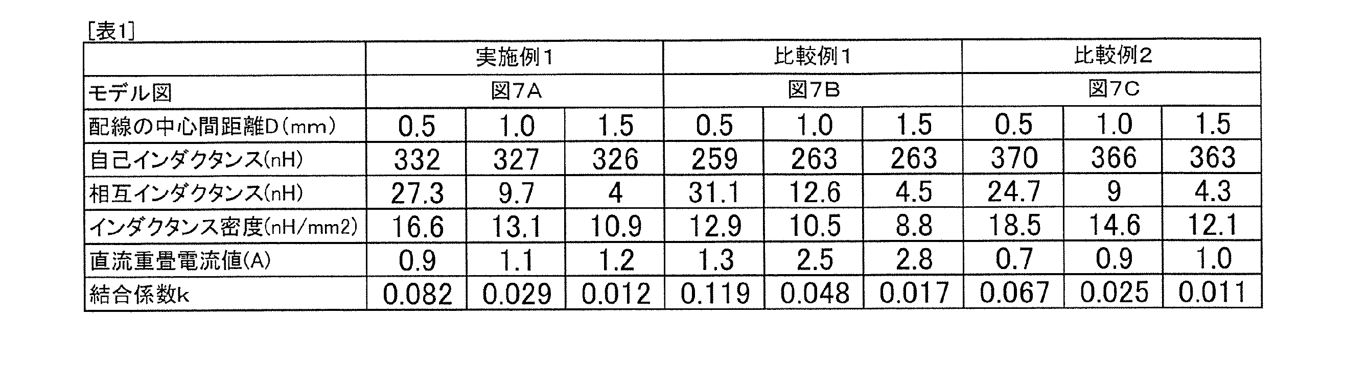
- Example 1 As a model similar to the embodiment of FIG. 5, the models shown in FIGS. 6 and 7A were used. In this model, the self-inductance, mutual inductance, inductance density, DC superimposition characteristics and coupling coefficient of the inductor were calculated by simulation under the conditions shown below.
- the inductance value for the DC magnetic field was calculated with the DC current applied to the wiring.
- the current value was swept from 0.1A to 100A.
- the inductance value when the DC current was 0.1 A was used as a reference (100%), and the value of the DC current when the DC current was reduced to 70% was calculated as the DC superimposed current value.
- Comparative Example 1 As shown in FIGS. 6 and 7B, the first embodiment is changed except that the center C2 of the first orientation region 31 is located on the first virtual line L2 and its vertical length is changed to 50 ⁇ m. Each value was calculated in the same manner as above. The results are shown in Table 1.
- the inductor of Example 1 has a lower coupling coefficient at any inter-wiring distance D1 than the inductor of Comparative Example 1, so that the influence between wirings is small and crosstalk Was reduced. Moreover, since the inductance density was high, the inductance was good. In addition, the decrease in inductance during DC current superimposition was small, and the DC superimposition characteristics were good.
- Example 1 had less decrease in inductance at the time of DC current superimposition and had good DC superimposition characteristics as compared with the inductor of Comparative Example 2.
- the inductor of the present invention can be used as a passive element such as a voltage conversion member, for example.
Landscapes
- Engineering & Computer Science (AREA)
- Power Engineering (AREA)
- Chemical & Material Sciences (AREA)
- Dispersion Chemistry (AREA)
- Microelectronics & Electronic Packaging (AREA)
- Coils Or Transformers For Communication (AREA)
- Soft Magnetic Materials (AREA)
Abstract
インダクタ(1)は、略円形状の複数の配線(2)と磁性層(3)とを備え、複数の配線(2)は、第1方向において、互いに間隔を隔てて配置されており、複数の配線(2)は、それぞれ、導線(6)と絶縁層(7)とを備え、磁性層(3)は、周辺領域において、それぞれ、異方性磁性粒子(8)が円周方向に沿って配向する第1領域(13)と、異方性磁性粒子(8)が円周方向に沿って配向していない第2領域(14)とを有し、第2領域(14)における仮想円弧(L1)の中心(C2)が、複数の配線(2)の中心(C1)を通る第1仮想線(L2)上に、存在しない。
Description
本発明は、インダクタに関する。
インダクタは、電子機器などに搭載されて、電圧変換部材などの受動素子として用いられることが知られている。
例えば、磁性体材料からなる直方体状のチップ本体部と、そのチップ本体部の内部に埋設された銅などの内部導体とを備え、チップ本体部の断面形状と内部導体の断面形状とが相似形であるインダクタが提案されている(特許文献1参照。)。すなわち、特許文献1のインダクタでは、断面視矩形状(直方体状)の配線(内部導体)の周囲に磁性体材料が被覆されている。
ところで、磁性体材料として、扁平状磁性粒子などの異方性磁性粒子を用いて、配線の周囲に、その異方性磁性粒子を配向させて、インダクタのインダクタンスを向上させることが検討されている。
しかしながら、特許文献1のインダクタでは、配線が、断面視矩形状であるため、角部などの存在によって、その配線の周囲に異方性磁性粒子を配向させにくい不具合が生じる。そのため、インダクタンスの向上が不十分となる場合がある。
そこで、断面視略円形状の配線を用いて、その配線の周囲に異方性磁性粒子を配向することがさらに検討される。
しかしながら、この方法では、直流重畳特性が不十分であり、さらなる改良が求められている。
加えて、複数の配線を備えるインダクタも要望されている。しかしながら、インダクタが複数の配線を備えると、隣り合う配線同士の磁気が影響し合い、ノイズが発生する不具合(クロストーク)が生じる。
本発明は、インダクタンスおよび直流重畳特性が良好であり、クロストークを抑制できるインダクタを提供する。
本発明[1]は、断面視略円形状の複数の配線と、前記複数の配線を被覆する磁性層とを備え、前記複数の配線は、第1方向において、互いに間隔を隔てて配置されており、前記複数の配線は、それぞれ、導線と、前記導線を被覆する絶縁層とを備え、前記磁性層は、異方性磁性粒子と、バインダとを含有し、前記磁性層は、前記複数の配線の周辺領域において、それぞれ、前記異方性磁性粒子が、前記配線の円周方向に沿って配向する第1領域と、前記異方性磁性粒子が、前記配線の円周方向に沿って配向していない第2領域とを有し、前記周辺領域は、断面視において、前記配線の重心から前記配線の外面までの距離の1.5倍値を、前記配線の前記外面から外側に進んだ領域であり、前記第2領域における円周方向一端と円周方向他端とを結ぶ仮想円弧の中心が、互いに隣り合う前記複数の配線の中心を通る第1仮想線上に、存在しない、インダクタを含む。
このインダクタによれば、複数の配線の周辺には、それぞれ、異方性磁性粒子が円周方向に沿って配向する第1領域が存在するため、インダクタンスが良好である。
また、複数の配線の周辺には、それぞれ、異方性磁性粒子が、前記配線の円周方向に沿って配向していない第2領域が存在するため、直流重畳特性が良好である。
また、第2領域における中心が、互いに隣り合う前記複数の配線の中心を通る第1仮想線上に、存在しない。したがって、磁束が第2領域を経由して一方の配線から他方の配線に到達する距離を長くすることができる。すなわち、配線間の磁束の距離を実質的に長くすることができる。よって、一方の配線から他方の配線への磁気に関する影響を低減でき、クロストークを抑制することができる。
本発明[2]は、前記仮想円弧の中心は、前記第1仮想線と、前記配線の中心を通り、前記第1仮想線と直交する第2仮想線との間に、位置する、[1]に記載のインダクタを含む。
このインダクタによれば、一方の磁性層に複数の配線を配置し、続いて、複数の配線が埋設されるように、他方の磁性層を一方の磁性層に積層することにより、第2領域の中心が、第1仮想線と第2仮想線との間に位置するインダクタを製造することができる。よって、[1]に記載のインダクタを容易に製造することができる。
本発明のインダクタによれば、インダクタンスおよび直流重畳特性が良好であり、クロストークを抑制することができる。
図1Aにおいて、紙面左右方向は、第1方向であって、紙面左側が第1方向一方側、紙面右側が第1方向他方側である。紙面上下方向は、第2方向(第1方向と直交する方向)であって、紙面上側が第2方向一方側(配線軸方向一方向)、紙面下側が第2方向他方側(配線軸他方向)である。紙面紙厚方向は、上下方向(第1方向および第2方向と直交する第3方向、厚み方向)であって、紙面手前側が上側(第3方向一方側、厚み方向一方側)、紙面奥側が下側(第3方向他方側、厚み方向他方側)である。具体的には、各図の方向矢印に準拠する。
<一実施形態>
1.インダクタ
本発明のインダクタの一実施形態を、図1A-図2を参照して説明する。
1.インダクタ
本発明のインダクタの一実施形態を、図1A-図2を参照して説明する。
図1A-Bに示すように、インダクタ1は、面方向(第1方向および第2方向)に延びる平面視略矩形状を有する。
インダクタ1は、図1A-図2に示すように、複数(2つ)の配線2と、磁性層3とを備える。
複数の配線2は、それぞれ、第1配線4と、第1配線4と幅方向(第1方向)に間隔を隔てて配置される第2配線5とを備える。
第1配線4は、図1A-Bに示すように、第2方向に長尺に延び、例えば、平面視略U字形状を有する。第1配線4は、図2に示すように、断面視略円形状を有する。
第1配線4は、導線6と、それを被覆する絶縁層7とを備える。
導線6は、第2方向に長尺に延び、例えば、平面視略U字形状を有する。また、導線6は、第1配線4と中心軸線を共有する断面視略円形状を有する。
導線6の材料は、例えば、銅、銀、金、アルミニウム、ニッケル、これらの合金などの金属導体であり、好ましくは、銅が挙げられる。導線6は、単層構造であってもよく、コア導体(例えば、銅)の表面にめっき(例えば、ニッケル)などがされた複層構造であってもよい。
導線6の半径R1は、例えば、25μm以上、好ましくは、50μm以上であり、また、例えば、2000μm以下、好ましくは、200μm以下である。
絶縁層7は、導線6を薬品や水から保護し、また、導線6の短絡を防止するための層である。絶縁層7は、導線6の外周面全面を被覆するように、配置されている。
絶縁層7は、第1配線4と中心軸線(中心C1)を共有する断面視略円環形状を有する。
絶縁層7の材料としては、例えば、ポリビニルホルマール、ポリエステル、ポリエステルイミド、ポリアミド(ナイロンを含む)、ポリイミド、ポリアミドイミド、ポリウレタンなどの絶縁性樹脂が挙げられる。これらは、1種単独で用いてもよく、2種以上併用してもよい。
絶縁層7は、単層から構成されていてもよく、複数の層から構成されていてもよい。
絶縁層7の厚みR2は、円周方向のいずれの位置においても配線2の径方向において略均一であり、例えば、1μm以上、好ましくは、3μm以上であり、また、例えば、100μm以下、好ましくは、50μm以下である。
絶縁層7の厚みR2に対する、導線6の半径R1の比(R1/R2)は、例えば、1以上、好ましくは、10以上であり、例えば、200以下、好ましくは、100以下である。
第1配線4の半径(R1+R2)は、例えば、25μm以上、好ましくは、50μm以上であり、また、例えば、2000μm以下、好ましくは、200μm以下である。
第1配線4が略U字形状である場合、第1配線4の中心間距離D2は、後述する複数の配線2間の中心間距離D1と同一距離であり、例えば、20μm以上、好ましくは、50μm以上であり、また、例えば、3000μm以下、好ましくは、2000μm以下である。
第2配線5は、第1配線4と同一形状であり、同一の構成、寸法および材料を備える。すなわち、第2配線5は、第1配線4と同様に、導線6と、それを被覆する絶縁層7とを備える。
第1配線4と第2配線5との中心間距離D1は、例えば、20μm以上、好ましくは、50μm以上であり、また、例えば、3000μm以下、好ましくは、2000μm以下である。
磁性層3は、インダクタンスを向上させるための層である。
磁性層3は、複数の配線2の外周面全面を被覆するように、配置されている。磁性層3は、インダクタ1の外形をなす。具体的には、磁性層3は、面方向(第1方向および第2方向)に延びる平面視略矩形状を有する。また、磁性層3は、その第2方向他方面において、複数の配線2の第2方向端縁を露出する。
磁性層3は、異方性磁性粒子8およびバインダ9を含有する磁性組成物から形成されている。
異方性磁性粒子(以下、「粒子」とも略する。)8を構成する磁性材料としては、軟磁性体、硬磁性体が挙げられる。好ましくは、インダクタンスの観点から、軟磁性体が挙げられる。
軟磁性体としては、例えば、1種類の金属元素を純物質の状態で含む単一金属体、例えば、1種類以上の金属元素(第1金属元素)と、1種類以上の金属元素(第2金属元素)および/または非金属元素(炭素、窒素、ケイ素、リンなど)との共融体(混合物)である合金体が挙げられる。これらは、単独または併用することができる。
単一金属体としては、例えば、1種類の金属元素(第1金属元素)のみからなる金属単体が挙げられる。第1金属元素としては、例えば、鉄(Fe)、コバルト(Co)、ニッケル(Ni)、その他、軟磁性体の第1金属元素として含有することが可能な金属元素の中から適宜選択される。
また、単一金属体としては、例えば、1種類の金属元素のみを含むコアと、そのコアの表面の一部または全部を修飾する無機物および/または有機物を含む表面層とを含む形態、例えば、第1金属元素を含む有機金属化合物や無機金属化合物が分解(熱分解など)された形態などが挙げられる。後者の形態として、より具体的には、第1金属元素として鉄を含む有機鉄化合物(具体的には、カルボニル鉄)が熱分解された鉄粉(カルボニル鉄粉と称される場合がある)などが挙げられる。なお、1種類の金属元素のみを含む部分を修飾する無機物および/または有機物を含む層の位置は、上記のような表面に限定されない。なお、単一金属体を得ることができる有機金属化合物や無機金属化合物としては、特に制限されず、軟磁性体の単一金属体を得ることができる公知乃至慣用の有機金属化合物や無機金属化合物から適宜選択することができる。
合金体は、1種類以上の金属元素(第1金属元素)と、1種類以上の金属元素(第2金属元素)および/または非金属元素(炭素、窒素、ケイ素、リンなど)との共融体であり、軟磁性体の合金体として利用することができるものであれば特に制限されない。
第1金属元素は、合金体における必須元素であり、例えば、鉄(Fe)、コバルト(Co)、ニッケル(Ni)などが挙げられる。なお、第1金属元素がFeであれば、合金体は、Fe系合金とされ、第1金属元素がCoであれば、合金体は、Co系合金とされ、第1金属元素がNiであれば、合金体は、Ni系合金とされる。
第2金属元素は、合金体に副次的に含有される元素(副成分)であり、第1金属元素に相溶(共融)する金属元素であって、例えば、鉄(Fe)(第1金属元素がFe以外である場合)、コバルト(Co)(第1金属元素がCo以外である場合)、ニッケル(Ni)(第1金属元素がNi以外である場合)、クロム(Cr)、アルミニウム(Al)、ケイ素(Si)、銅(Cu)、銀(Ag)、マンガン(Mn)、カルシウム(Ca)、バリウム(Ba)、チタン(Ti)、ジルコニウム(Zr)、ハフニウム(Hf)、バナジウム(V)、ニオブ(Nb)、タンタル(Ta)、モリブデン(Mo)、タングステン(W)、ルテニウム(Ru)、ロジウム(Rh)、亜鉛(Zn)、ガリウム(Ga)、インジウム(In)、ゲルマニウム(Ge)、スズ(Sn)、鉛(Pb)、スカンジウム(Sc)、イットリウム(Y)、ストロンチウム(Sr)、各種希土類元素などが挙げられる。これらは、単独使用または2種以上併用することができる。
非金属元素は、合金体に副次的に含有される元素(副成分)であり、第1金属元素に相溶(共融)する非金属元素であって、例えば、ホウ素(B)、炭素(C)、窒素(N)、ケイ素(Si)、リン(P)、硫黄(S)などが挙げられる。これらは、単独使用または2種以上併用することができる。
合金体の一例であるFe系合金として、例えば、磁性ステンレス(Fe-Cr-Al-Si合金)(電磁ステンレスを含む)、センダスト(Fe-Si-Al合金)(スーパーセンダストを含む)、パーマロイ(Fe-Ni合金)、Fe-Ni-Mo合金、Fe-Ni-Mo-Cu合金、Fe-Ni-Co合金、Fe-Cr合金、Fe-Cr-Al合金、Fe-Ni-Cr合金、Fe-Ni-Cr-Si合金、ケイ素銅(Fe-Cu-Si合金)、Fe-Si合金、Fe-Si―B(-Cu-Nb)合金、Fe-B-Si-Cr合金、Fe-Si-Cr-Ni合金、Fe-Si-Cr合金、Fe-Si-Al-Ni-Cr合金、Fe-Ni-Si-Co合金、Fe-N合金、Fe-C合金、Fe-B合金、Fe-P合金、フェライト(ステンレス系フェライト、さらには、Mn-Mg系フェライト、Mn-Zn系フェライト、Ni-Zn系フェライト、Ni-Zn-Cu系フェライト、Cu-Zn系フェライト、Cu-Mg-Zn系フェライトなどのソフトフェライトを含む)、パーメンジュール(Fe-Co合金)、Fe-Co-V合金、Fe基アモルファス合金などが挙げられる。
合金体の一例であるCo系合金としては、例えば、Co-Ta-Zr、コバルト(Co)基アモルファス合金などが挙げられる。
合金体の一例であるNi系合金としては、例えば、Ni-Cr合金などが挙げられる。
これら軟磁性体の中でも、磁気特性の点から、好ましくは、合金体、より好ましくは、Fe系合金、さらに好ましくは、センダスト(Fe-Si-Al合金)が挙げられる。また、軟磁性体として、好ましくは、単一金属体、より好ましくは、鉄元素を純物質の状態で含む単一金属体、さらに好ましくは、鉄単体、あるいは、鉄粉(カルボニル鉄粉)が挙げられる。
粒子8の形状としては、異方性の観点から、例えば、扁平状(板状)、針状などが挙げられ、好ましくは、面方向(二次元)に比透磁率が良好である観点から、扁平状が挙げられる。なお、磁性層3は、異方性磁性粒子8に加え、非異方性磁性粒子をさらに含有することもできる。非異方性磁性粒子は、例えば、球状、顆粒状、塊状、ペレット状などの形状を有していてもよい。非異方性磁性粒子の平均粒子径は、例えば、0.1μm以上、好ましくは、0.5μm以上であり、また、例えば、200μm以下、好ましくは、150μm以下である。
なお、扁平状の粒子8の扁平率(扁平度)は、例えば、8以上、好ましくは、15以上であり、また、例えば、500以下、好ましくは、450以下である。扁平率は、例えば、粒子8の平均粒子径(平均長さ)(後述)を粒子8の平均厚さで除したアスペクト比として算出される。
粒子8(異方性磁性粒子)の平均粒子径(平均長さ)は、例えば、3.5μm以上、好ましくは、10μm以上であり、また、例えば、200μm以下、好ましくは、150μm以下である。粒子8が扁平状であれば、その平均厚みが、例えば、0.1μm以上、好ましくは、0.2μm以上であり、また、例えば、3.0μm以下、好ましくは、2.5μm以下である。
バインダ9としては、例えば、熱硬化性樹脂、熱可塑性樹脂が挙げられる。
熱硬化性樹脂としては、例えば、エポキシ樹脂、フェノール樹脂、メラミン樹脂、熱硬化性ポリイミド樹脂、不飽和ポリエステル樹脂、ポリウレタン樹脂、シリコーン樹脂などが挙げられる。接着性、耐熱性などの観点から、好ましくは、エポキシ樹脂、フェノール樹脂が挙げられる。
熱可塑性樹脂としては、例えば、アクリル樹脂、エチレン-酢酸ビニル共重合体、ポリカーボネート樹脂、ポリアミド樹脂(6-ナイロン、6,6-ナイロンなど)、熱可塑性ポリイミド樹脂、飽和ポリエステル樹脂(PET、PBTなど)などが挙げられる。好ましくは、アクリル樹脂が挙げられる。
好ましくは、バインダ9として、熱硬化性樹脂および熱可塑性樹脂の併用が挙げられる。より好ましくは、アクリル樹脂、エポキシ樹脂およびフェノール樹脂の併用が挙げられる。これにより、粒子8を所定の配向状態で、かつ、高充填で、配線2の周囲により確実に固定できる。
また、磁性組成物は、必要に応じて、熱硬化触媒、無機粒子、有機粒子、架橋剤などの添加剤を含有することもできる。
磁性層3では、粒子8がバインダ9内に配向しながら均一に配置されている。
磁性層3は、断面視において、周辺領域11と、外側領域12とを有する。
周辺領域11は、配線2の周辺領域であって、複数の配線2と接触するように複数の配線2の周囲に位置する。周辺領域11は、配線2と中心軸線を共有する断面視略円環状を有する。より具体的には、周辺領域11は、磁性層3のうち、配線2の半径(配線2の中心(重心)C1から外周面までの距離;R1+R2)の1.5倍値(好ましくは、1.2倍値、より好ましくは、1倍値、さらに好ましくは、0.8倍値、とりわけ好ましくは、0.5倍値)、配線2の外周面から径方向外側に進んだ領域である。
周辺領域11は、複数の配線2のそれぞれの周囲、すなわち、第1配線4および第2配線5の周囲に配置されている。
周辺領域11は、それぞれ、複数(2つ)の第1領域13と、複数(2つ)の第2領域14とを備える。
複数の第1領域13は、円周方向配向領域である。すなわち、第1領域13では、粒子8が配線2(第1配線4または第2配線5)の円周方向に沿って配向する。
複数の第1領域13は、配線2の上側(第3方向一方側)および下側(第3方向他方側)に、配線2の中心C1を挟んで互いに対向配置されている。すなわち、複数の第1領域13は、配線2の上側に配置される上側第1領域15と、配線2の下側に配置される下側第1領域16とを備える。また、上側第1領域15と下側第1領域16との上下方向中央に、配線2の中心C1が位置する。
それぞれの第1領域13では、粒子8の比透磁率が高い方向(例えば、扁平状異方性磁性粒子では、粒子の面方向)が、配線2の中心C1を中心とした円の接線と略一致する。
より具体的には、粒子8の面方向と、その粒子8が位置する円の接線とがなす角度が、15°以下である場合を、粒子8が円周方向に配向していると定義する。
より具体的には、粒子8の面方向と、その粒子8が位置する円の接線とがなす角度が、15°以下である場合を、粒子8が円周方向に配向していると定義する。
第1領域13に含まれる粒子8全体の数に対して、円周方向に配向している粒子8の数の割合は、例えば、50%を超過し、好ましくは、70%以上、より好ましくは、80%以上である。すなわち、第1領域13では、円周方向に配向していない粒子8を、例えば、50%未満、好ましくは、30%以下、より好ましくは、20%以下含んでいてもよい。
複数の第1領域13の総面積割合は、周辺領域11全体に対して、例えば、40%以上、好ましくは、50%以上、より好ましくは、60%以上であり、また、例えば、90%以下、好ましくは、80%以下である。
第1領域13の円周方向の比透磁率は、例えば、5以上、好ましくは、10以上、より好ましくは、30以上であり、また、例えば、500以下である。径方向の比透磁率は、例えば、1以上、好ましくは、5以上であり、また、例えば、100以下、好ましくは、50以下、より好ましくは、25以下である。また、径方向に対する円周方向の比透磁率の比(円周方向/径方向)は、例えば、2以上、好ましくは、5以上であり、また、例えば、50以下である。比透磁率が上記範囲であれば、インダクタンスに優れる。
比透磁率は、例えば、磁性材料テストフィクスチャを使用したインピーダンスアナライザ(Agilent社製、「4291B」)によって測定することができる。
複数の第2領域14は、円周方向非配向領域である。すなわち、第2領域14では、粒子8が、配線2の円周方向に沿って配向していない。換言すると、第2領域14では、粒子8が、配線2の円周方向以外の方向(例えば、第1方向や径方向)に沿って配向するか、または、配向していない。
複数の第2領域14は、配線2の第1方向一方側および他方側に、配線2を挟んで互いに対向配置されている。すなわち、複数の第2領域14は、配線2(第1配線4または第2配線5)の第1方向一方側に配置される一方側第2領域17と、配線2の第1方向他方側に配置される他方側第2領域18とを有する。一方側第2領域17と他方側第2領域18とは、第2仮想線L3を基準に略線対称である。
なお、第2仮想線L3は、第1配線4または第2配線5の中心C1を通り、かつ、上下方向に延びる直線である。
それぞれの第2領域14では、粒子8の比透磁率が高い方向(例えば、扁平状異方性磁性粒子では、粒子の面方向)が、配線2の中心C1を中心とした円の接線と一致しない。
より具体的には、粒子8の面方向と、その粒子8が位置する円の接線とがなす角度が、15°を超過する場合を、粒子8が円周方向に配向していないと定義する。
より具体的には、粒子8の面方向と、その粒子8が位置する円の接線とがなす角度が、15°を超過する場合を、粒子8が円周方向に配向していないと定義する。
第2領域14に含まれる粒子8全体の数に対して、円周方向に配向していない粒子8の数の割合は、50%を超過し、好ましくは、70%以上であり、また、例えば、95%以下、好ましくは、90%以下である。
第2領域14では、例えば、円周方向に配向する粒子8を含んでいてもよい。第2領域14に含まれる粒子8全体の数に対して、円周方向に配向する粒子8の数の割合は、50%未満であり、好ましくは、30%以下であり、また、例えば、5%以上、好ましくは、10%以上である。
なお、円周方向に配向する粒子8を含む場合、好ましくは、その円周方向に配向する粒子8は、第2領域14の最内側、すなわち、配線2の表面に配置されている。
複数の第2領域14の総面積割合は、周辺領域11全体に対して、例えば、10%以上、好ましくは、20%以上であり、また、例えば、60%以下、好ましくは、50%以下、より好ましくは、40%以下である。
第2領域14の中心C2は、第1仮想線L2上に存在しない。すなわち、中心C2は、第1仮想線L2に対し、下側に位置し、好ましくは、第1仮想線L2に対し、半径Rの0.1倍の距離分、下方に位置し、より好ましくは、第1仮想線L2に対し、半径Rの0.3倍の距離分、下方に位置する。より具体的には、中心C2は、第1仮想線L2に対し、好ましくは、10μm下方、より好ましくは、30μm下方に位置する。
また、第2領域14の中心C2は、第1仮想線L2と第2仮想線L3との間に、位置する。すなわち、第2領域14の中心C2は、第1仮想線L2および第2仮想線L3のいずれの線上にも存在しない。
なお、第2領域14の中心C2は、第2領域14において、円周方向一端と円周方向他端とを結ぶ仮想円弧L1の中心である。より具体的には、第2領域14の中心C2は、第2領域14において、円周方向一端縁の径方向中心と、円周方向他端縁の径方向中心とを結ぶ仮想円弧L1の中心である。
第1仮想線L2は、互いに隣り合う複数の配線2の中心C1を通り、第1方向に延びる直線である。
第2領域14では、配向方向が異なる少なくとも2種類の粒子8により交差部(頂部)19が形成されている。すなわち、第2領域14内において相対的に上側に位置し、且つ配線2の円周方向において第2領域14の下端側に向かうに従って円周方向から第1方向に配向する粒子8(第1粒子)と、第2領域14内において相対的に下側(第1粒子よりも下側)に位置し、且つ円周方向において第2領域14の上端側に向かうに従って円周方向から第1方向に配向する粒子8(第2粒子)とが、略三角形状の少なくとも2辺を構成して、これによって、交差部19を形成する。具体的には、第1粒子と、第2粒子とは、第2領域14の内側において円周方向に配向する粒子8(第3粒子)とともに、略三角形状(好ましくは、鋭角三角形状)を形成する。
交差部19は、第1配線4および第2配線5の間において、それらの中心を通る第1仮想線L2上に、存在しない。すなわち、交差部19は、第1仮想線L2の下側に、第1仮想線L2と間隔を隔てる位置に配置されている。より具体的には、交差部19の中心および配線2の中心C1を結ぶ直線と、第1仮想線L2とのなす角度θは、例えば、15°以上、好ましくは、45°以上であり、また、例えば、75°以下、好ましくは、60°以下である。
周辺領域11(特に、第1領域13および第2領域14のそれぞれ)において、粒子8の充填率は、例えば、40体積%以上、好ましくは、45体積%以上であり、また、例えば、90体積%以下、好ましくは、70体積%以下である。充填率が上記下限以上であれば、インダクタンスに優れる。
充填率は、実比重の測定、SEM写真断面図の二値化などによって算出することができる。
周辺領域11において、複数の第1領域13と複数の第2領域14とは、円周方向に互いに隣接するように、配置されている。具体的には、上側第1領域15、一方側第2領域17、下側第1領域16および他方側第2領域18は、円周方向に、この順で連続する。なお、第1領域13と第2領域14との円周方向における境界(一端縁または他端縁)は、配線2の中心から径方向外側に延びる仮想直線とする。
外側領域12は、磁性層3のうち、周辺領域11以外の領域である。外側領域12は、周辺領域11の外側において、周辺領域11と連続するように配置されている。
外側領域12では、粒子8が面方向(特に第1方向)に沿って配向している。
外側領域12では、粒子8の比透磁率が高い方向(例えば、扁平状異方性磁性粒子では、粒子の面方向)が、第1方向と略一致する。より具体的には、粒子8の面方向と、第1方向とがなす角度が、15°以下である場合を、粒子8が第1方向に配向していると定義する。
外側領域12では、外側領域12に含まれる粒子8全体の数に対して、第1方向に配向している粒子8の数の割合が、50%を超過し、好ましくは、70%以上、より好ましくは、90%以上である。すなわち、外側領域12では、第1方向に配向していない粒子8を50%未満、好ましくは、30%以下、より好ましくは、10%以下含んでいてもよい。
外側領域12において、第1方向の比透磁率は、例えば、5以上、好ましくは、10以上、より好ましくは、30以上であり、また、例えば、500以下である。上下方向の比透磁率は、例えば、1以上、好ましくは、5以上であり、また、例えば、100以下、好ましくは、50以下、より好ましくは、25以下である。また、上下方向に対する第1方向の比透磁率の比(第1方向/上下方向)は、例えば、2以上、好ましくは、5以上であり、また、例えば、50以下である。比透磁率が上記範囲であれば、インダクタンスに優れる。
外側領域12において、粒子8の充填率は、例えば、40体積%以上、好ましくは、45体積%以上であり、また、例えば、90体積%以下、好ましくは、70体積%以下である。充填率が上記下限以上であれば、インダクタンスに優れる。
磁性層3の第1方向長さT1は、例えば、5mm以上、好ましくは、10mm以上であり、また、例えば、5000mm以下、好ましくは、2000mm以下である。
磁性層3の第2方向長さT2は、例えば、5mm以上、好ましくは、10mm以上であり、また、例えば、5000mm以下、好ましくは、2000mm以下である。
磁性層3の上下方向長さ(厚さ)T3は、例えば、100μm以上、好ましくは、200μm以上であり、また、例えば、2000μm以下、好ましくは、1000μm以下である。
2.インダクタの製造方法
図3A-Bを参照して、インダクタ1の製造方法の一実施形態について説明する。インダクタ1の製造方法は、例えば、用意工程、配置工程および積層工程を順に備える。
図3A-Bを参照して、インダクタ1の製造方法の一実施形態について説明する。インダクタ1の製造方法は、例えば、用意工程、配置工程および積層工程を順に備える。
用意工程では、複数の配線2、および、2つの異方性磁性シート20を用意する。
2つの異方性磁性シート20は、それぞれ、面方向に延びるシート状を有し、磁性組成物から形成されている。異方性磁性シート20では、粒子8が、面方向に配向されている。好ましくは、2つの半硬化状態(Bステージ)の異方性磁性シート20を用いる。
このような異方性磁性シート20としては、特開2014-165363号、特開2015-92544号などに記載の軟磁性熱硬化性接着フィルムや軟磁性フィルムなどが挙げられる。
配置工程では、図3Aに示すように、一方の異方性磁性シート20の上面に複数の配線2を配置するとともに、複数の配線2の上方に、他方の異方性磁性シート20を対向配置する。
具体的には、下側異方性磁性シート21を水平台に載置し、続いて、下側異方性磁性シート21の上面に複数の配線2を第1方向に所望の間隔を隔てて配置する。
次いで、上側異方性磁性シート22を、下側異方性磁性シート21および複数の配線2の上側に、間隔を隔てて対向配置する。
積層工程では、図3Bに示すように、複数の配線2を埋設するように、2つの異方性磁性シート20を、積層する。
具体的には、上側異方性磁性シート22を下側に向かって押圧する。
この際、2つの異方性磁性シート20が半硬化状態である場合は、押圧によって、複数の配線2は、下側異方性磁性シート21内にわずかに沈み込み、沈み込み部分において、粒子8が複数の配線2に沿って配向する。すなわち、下側第1領域16が形成される。
また、上側異方性磁性シート22は、複数の配線2に沿って被覆され、その粒子8が複数の配線2に沿って配向するとともに、下側異方性磁性シート21の上面に積層される。
すなわち、配線2の上側では、上側異方性磁性シート22によって、上側第1領域15が形成されるとともに、配線2の第1方向両側(側方)では、下側異方性磁性シート21と上側異方性磁性シート22との接触付近にて、これらに配向している粒子8が衝突し、その結果、第2領域14や交差部19が形成される。
すなわち、配線2の上側では、上側異方性磁性シート22によって、上側第1領域15が形成されるとともに、配線2の第1方向両側(側方)では、下側異方性磁性シート21と上側異方性磁性シート22との接触付近にて、これらに配向している粒子8が衝突し、その結果、第2領域14や交差部19が形成される。
なお、異方性磁性シート20が半硬化状態である場合は、加熱する。これにより、異方性磁性シート20が硬化状態(Cステージ)となる。また、2つの異方性磁性シート20の接触界面25が消滅し、2つの異方性磁性シート20は、一の磁性層3を形成する。
これにより、図2に示すように、断面視略円形状の配線2と、それを被覆する磁性層3とを備えるインダクタ1が得られる。すなわち、インダクタ1は、複数(2つ)の異方性磁性シート20を、配線2を挟むように、積層してなるものである。なお、実際のインダクタ1の一例の断面図(SEM写真)を図4に示す。
3.用途
インダクタ1は、電子機器の一部品、すなわち、電子機器を作製するための部品であり、電子素子(チップ、キャパシタなど)や、電子素子を実装する実装基板を含まず、部品単独で流通し、産業上利用可能なデバイスである。
インダクタ1は、電子機器の一部品、すなわち、電子機器を作製するための部品であり、電子素子(チップ、キャパシタなど)や、電子素子を実装する実装基板を含まず、部品単独で流通し、産業上利用可能なデバイスである。
インダクタ1は、例えば、電子機器などに搭載される(組み込まれる)。図示しないが、電子機器は、実装基板と、実装基板に実装される電子素子(チップ、キャパシタなど)とを備える。そして、インダクタ1は、はんだなどの接続部材を介して実装基板に実装され、他の電子機器と電気的に接続され、コイルなどの受動素子として作用する。
そして、インダクタ1によれば、複数の配線2の周辺領域11には、それぞれ、粒子8が円周方向に沿って配向する第1領域13が存在するため、インダクタンスが良好である。
また、複数の配線2の周辺領域11には、それぞれ、粒子8が円周方向に沿って配向していない第2領域14が存在するため、直流重畳特性が良好である。
また、第2領域14における中心C2が、第1仮想線L2上に、存在しない。したがって、磁束が第2領域14を経由して第1配線4から第2配線5に到達する距離を長くすることができる。すなわち、配線2間の磁束が通る距離を実質的に長くすることができる。
よって、第1配線4から第2配線5への磁気に関する影響を低減でき、クロストークを抑制することができる。
よって、第1配線4から第2配線5への磁気に関する影響を低減でき、クロストークを抑制することができる。
また、第2領域14の中心C2は、円周方向において、第1仮想線L2と第2仮想線L3との間に、位置する。このため、図3A-Bに示すように、下側の異方性磁性シート21の上面に複数の配線2を配置し、続いて、複数の配線2が埋設されるように、上側の異方性磁性シート22を下側の異方性磁性シート21に積層することにより、第2領域14を上記位置に容易に配置することができる。よって、インダクタンスおよび直流重畳特性が良好であり、クロストークを抑制できるインダクタ1を容易に得ることができる。
<変形例>
図5を参照して、図1A-図2に示す一実施形態の変形例について説明する。なお、変形例において、上記した一実施形態と同様の部材には、同様の符号を付し、その説明を省略する。これら変形例についても、上記した一実施形態などと同様の作用効果を奏する。
図5を参照して、図1A-図2に示す一実施形態の変形例について説明する。なお、変形例において、上記した一実施形態と同様の部材には、同様の符号を付し、その説明を省略する。これら変形例についても、上記した一実施形態などと同様の作用効果を奏する。
図2に示す実施形態では、交差部19の上下方向位置は、配線2の中心C1と配線2の最下端との間であるが、例えば、図5に示すように、交差部19の上下方向位置は、配線2の最下端と同一位置とすることができる。
図5に示す実施形態は、例えば、2つの異方性磁性シート20として、硬化状態の下側異方性磁性シート21と、半硬化状態の上側異方性磁性シート22とを用いる。これにより、複数の配線2は、下側異方性磁性シート21に沈み込まないため、図5に示すインダクタ1を容易に製造することができる。
図1A-Bに示す実施形態では、2つの配線2を備えているが、その数は、限定されず、3つ以上とすることもできる。
図1A-Bに示す実施形態では、各配線2は、平面視略U字形状を有しているが、その形状は限定されず、適宜設定できる。
図1A-Bに示す実施形態において、磁性層3がアライメントマークを有することもできる。
図1A-Bに示す実施形態において、磁性層3における異方性磁性粒子8の割合は、磁性層3において一様でもよく、また、各配線2から離れるに従って、高くなってもよく、あるいは、低くなってもよい。
<シミュレーション結果>
実施例1
図5の実施形態に類似したモデルとして、図6および図7Aに示すモデルを用いた。このモデルにおいて、下記に示す条件にて、インダクタの自己インダクタンス、相互インダクタンス、インダクタンス密度、直流重畳特性および結合係数をシミュレーションによって算出した。
実施例1
図5の実施形態に類似したモデルとして、図6および図7Aに示すモデルを用いた。このモデルにおいて、下記に示す条件にて、インダクタの自己インダクタンス、相互インダクタンス、インダクタンス密度、直流重畳特性および結合係数をシミュレーションによって算出した。
ソフト:ANSYS社製の「Maxwell 3D」、導線6の半径R1:110μm、絶縁層7の厚みR2:5μm、磁性層3の第1方向長さT1:14.5mm、磁性層3の第2方向長さT2:12mm、配線2の第2方向長さ:10mm、磁性層3の厚みT3:430μm、周辺領域11の径方向長さ:60μm、円周方向配向領域30の周方向の比透磁率μ:140、円周方向配向領域30の径方向の比透磁率μ:10、第1方向配向領域31の第1方向の比透磁率μ:140、第1方向配向領域31の上下方向の比透磁率μ:10、第1方向配向領域31の上下方向距離:60μm、周波数:10MHz、配線2間の中心間距離D1:0.5mm、1.0mm、または、1.5mm
・直流重畳特性は、外部の磁界強度Hに対する磁気特性Bの変化を設定した。また、面方向に対しては非線形(外部の磁界強度Hが強くなると徐々にBが飽和するモード)で設定し、厚み方向に対しては、線形(外部の磁界強度Hに対してBが常に一定で飽和しないモード)で設定した。
・直流重畳特性は、外部の磁界強度Hに対する磁気特性Bの変化を設定した。また、面方向に対しては非線形(外部の磁界強度Hが強くなると徐々にBが飽和するモード)で設定し、厚み方向に対しては、線形(外部の磁界強度Hに対してBが常に一定で飽和しないモード)で設定した。
配線に直流電流を印加した状態で、直流磁界に対するインダクタンス値を算出した。
電流値を0.1A~100Aまで掃引した。この際、直流電流が0.1Aである際のインダクタンス値を基準(100%)とし、70%に低下した際の直流電流の値を、直流重畳電流値として、算出した。
これらの結果を表1に示す。
比較例1
図6および図7Bに示すように、第1方向配向領域31の中心C2が第1仮想線L2上に位置するように変更し、その上下方向長さを50μmに変更した以外は、実施例1と同様にして、各値を算出した。結果を表1に示す。
図6および図7Bに示すように、第1方向配向領域31の中心C2が第1仮想線L2上に位置するように変更し、その上下方向長さを50μmに変更した以外は、実施例1と同様にして、各値を算出した。結果を表1に示す。
比較例2
図6および図7Cに示すように、第1方向配向領域31を配置せず、周辺領域11を円周方向配向領域のみとした以外は、実施例1と同様にして、各値を算出した。結果を表1に示す。
図6および図7Cに示すように、第1方向配向領域31を配置せず、周辺領域11を円周方向配向領域のみとした以外は、実施例1と同様にして、各値を算出した。結果を表1に示す。
考察
表1から明らかなように、実施例1のインダクタは、比較例1のインダクタと比較して、いずれの配線間距離D1においても、結合係数が低いため、配線間の影響が少なく、クロストークが低減されていた。また、インダクタンス密度が高いため、インダクタンスが良好であった。また、直流電流重畳時のインダクタンスの低下が少なく、直流重畳特性が良好であった。
表1から明らかなように、実施例1のインダクタは、比較例1のインダクタと比較して、いずれの配線間距離D1においても、結合係数が低いため、配線間の影響が少なく、クロストークが低減されていた。また、インダクタンス密度が高いため、インダクタンスが良好であった。また、直流電流重畳時のインダクタンスの低下が少なく、直流重畳特性が良好であった。
また、実施例1のインダクタは、比較例2のインダクタと比較して、直流電流重畳時のインダクタンスの低下が少なく、直流重畳特性が良好であった。
本発明のインダクタは、例えば、電圧変換部材などの受動素子として用いることができる。
1 インダクタ
2 配線
3 磁性層
6 導線
7 絶縁層
8 異方性磁性粒子
13 第1領域
14 第2領域
C1 配線の中心
C2 仮想円弧の中心
L1 仮想円弧
L2 第1仮想線
L3 第2仮想線
2 配線
3 磁性層
6 導線
7 絶縁層
8 異方性磁性粒子
13 第1領域
14 第2領域
C1 配線の中心
C2 仮想円弧の中心
L1 仮想円弧
L2 第1仮想線
L3 第2仮想線
Claims (2)
- 断面視略円形状の複数の配線と、前記複数の配線を被覆する磁性層とを備え、
前記複数の配線は、第1方向において、互いに間隔を隔てて配置されており、
前記複数の配線は、それぞれ、導線と、前記導線を被覆する絶縁層とを備え、
前記磁性層は、異方性磁性粒子と、バインダとを含有し、
前記磁性層は、前記複数の配線の周辺領域において、それぞれ、
前記異方性磁性粒子が、前記配線の円周方向に沿って配向する第1領域と、
前記異方性磁性粒子が、前記配線の円周方向に沿って配向していない第2領域と
を有し、
前記周辺領域は、断面視において、前記配線の重心から前記配線の外面までの距離の1.5倍値を、前記配線の前記外面から外側に進んだ領域であり、
前記第2領域における円周方向一端と円周方向他端とを結ぶ仮想円弧の中心が、互いに隣り合う前記複数の配線の中心を通る第1仮想線上に、存在しないことを特徴とする、インダクタ。 - 前記仮想円弧の中心は、前記第1仮想線と、前記配線の中心を通り、前記第1仮想線と直交する第2仮想線との間に、位置することを特徴とする、請求項1に記載のインダクタ。
Priority Applications (2)
| Application Number | Priority Date | Filing Date | Title |
|---|---|---|---|
| CN202080019771.9A CN113544802B (zh) | 2019-03-12 | 2020-02-05 | 电感器 |
| KR1020217028622A KR102728438B1 (ko) | 2019-03-12 | 2020-02-05 | 인덕터 |
Applications Claiming Priority (2)
| Application Number | Priority Date | Filing Date | Title |
|---|---|---|---|
| JP2019044769A JP7219641B2 (ja) | 2019-03-12 | 2019-03-12 | インダクタ |
| JP2019-044769 | 2019-03-12 |
Publications (1)
| Publication Number | Publication Date |
|---|---|
| WO2020183989A1 true WO2020183989A1 (ja) | 2020-09-17 |
Family
ID=72427369
Family Applications (1)
| Application Number | Title | Priority Date | Filing Date |
|---|---|---|---|
| PCT/JP2020/004223 Ceased WO2020183989A1 (ja) | 2019-03-12 | 2020-02-05 | インダクタ |
Country Status (5)
| Country | Link |
|---|---|
| JP (1) | JP7219641B2 (ja) |
| KR (1) | KR102728438B1 (ja) |
| CN (1) | CN113544802B (ja) |
| TW (1) | TWI826648B (ja) |
| WO (1) | WO2020183989A1 (ja) |
Citations (5)
| Publication number | Priority date | Publication date | Assignee | Title |
|---|---|---|---|---|
| JP2003282333A (ja) * | 2002-03-27 | 2003-10-03 | Tdk Corp | コイル封入圧粉磁芯 |
| JP2008172873A (ja) * | 2007-01-09 | 2008-07-24 | Sony Ericsson Mobilecommunications Japan Inc | 無接点電力伝送コイル、携帯端末及び端末充電装置、平面コイルの磁性体層形成装置及び磁性体層形成方法 |
| JP2016092422A (ja) * | 2014-10-31 | 2016-05-23 | サムソン エレクトロ−メカニックス カンパニーリミテッド. | コイル部品アセンブリ、コイル部品及びその製造方法 |
| WO2016199638A1 (ja) * | 2015-06-10 | 2016-12-15 | 日東電工株式会社 | コイルモジュールおよびその製造方法 |
| WO2019244620A1 (ja) * | 2018-06-21 | 2019-12-26 | 日東電工株式会社 | インダクタ |
Family Cites Families (6)
| Publication number | Priority date | Publication date | Assignee | Title |
|---|---|---|---|---|
| JPH10144526A (ja) | 1996-11-05 | 1998-05-29 | Murata Mfg Co Ltd | 積層チップインダクタ |
| JP5054445B2 (ja) * | 2007-06-26 | 2012-10-24 | スミダコーポレーション株式会社 | コイル部品 |
| JP5710427B2 (ja) * | 2011-08-31 | 2015-04-30 | 株式会社東芝 | 磁性材料、磁性材料の製造方法および磁性材料を用いたインダクタ素子 |
| JP2014175349A (ja) * | 2013-03-06 | 2014-09-22 | Murata Mfg Co Ltd | 積層インダクタ |
| JP6479074B2 (ja) * | 2016-08-30 | 2019-03-06 | サムソン エレクトロ−メカニックス カンパニーリミテッド. | 磁性体組成物、インダクタおよび磁性体本体 |
| JP6953279B2 (ja) * | 2016-12-07 | 2021-10-27 | 日東電工株式会社 | モジュールの製造方法 |
-
2019
- 2019-03-12 JP JP2019044769A patent/JP7219641B2/ja active Active
-
2020
- 2020-02-05 CN CN202080019771.9A patent/CN113544802B/zh active Active
- 2020-02-05 WO PCT/JP2020/004223 patent/WO2020183989A1/ja not_active Ceased
- 2020-02-05 KR KR1020217028622A patent/KR102728438B1/ko active Active
- 2020-02-17 TW TW109104914A patent/TWI826648B/zh active
Patent Citations (5)
| Publication number | Priority date | Publication date | Assignee | Title |
|---|---|---|---|---|
| JP2003282333A (ja) * | 2002-03-27 | 2003-10-03 | Tdk Corp | コイル封入圧粉磁芯 |
| JP2008172873A (ja) * | 2007-01-09 | 2008-07-24 | Sony Ericsson Mobilecommunications Japan Inc | 無接点電力伝送コイル、携帯端末及び端末充電装置、平面コイルの磁性体層形成装置及び磁性体層形成方法 |
| JP2016092422A (ja) * | 2014-10-31 | 2016-05-23 | サムソン エレクトロ−メカニックス カンパニーリミテッド. | コイル部品アセンブリ、コイル部品及びその製造方法 |
| WO2016199638A1 (ja) * | 2015-06-10 | 2016-12-15 | 日東電工株式会社 | コイルモジュールおよびその製造方法 |
| WO2019244620A1 (ja) * | 2018-06-21 | 2019-12-26 | 日東電工株式会社 | インダクタ |
Also Published As
| Publication number | Publication date |
|---|---|
| CN113544802B (zh) | 2026-02-13 |
| JP7219641B2 (ja) | 2023-02-08 |
| CN113544802A (zh) | 2021-10-22 |
| KR102728438B1 (ko) | 2024-11-08 |
| TW202034356A (zh) | 2020-09-16 |
| JP2020150058A (ja) | 2020-09-17 |
| KR20210132073A (ko) | 2021-11-03 |
| TWI826648B (zh) | 2023-12-21 |
Similar Documents
| Publication | Publication Date | Title |
|---|---|---|
| JP7030022B2 (ja) | インダクタ | |
| JP7286354B2 (ja) | インダクタ | |
| JP7325197B2 (ja) | インダクタ | |
| US12198843B2 (en) | Inductor | |
| KR102852328B1 (ko) | 인덕터 | |
| JP7249823B2 (ja) | インダクタ | |
| KR20210137028A (ko) | 인덕터 | |
| JP7219641B2 (ja) | インダクタ | |
| JP7294833B2 (ja) | インダクタ |
Legal Events
| Date | Code | Title | Description |
|---|---|---|---|
| 121 | Ep: the epo has been informed by wipo that ep was designated in this application |
Ref document number: 20770578 Country of ref document: EP Kind code of ref document: A1 |
|
| ENP | Entry into the national phase |
Ref document number: 20217028622 Country of ref document: KR Kind code of ref document: A |
|
| NENP | Non-entry into the national phase |
Ref country code: DE |
|
| 122 | Ep: pct application non-entry in european phase |
Ref document number: 20770578 Country of ref document: EP Kind code of ref document: A1 |