WO2020183812A1 - 半導体発光装置 - Google Patents
半導体発光装置 Download PDFInfo
- Publication number
- WO2020183812A1 WO2020183812A1 PCT/JP2019/046854 JP2019046854W WO2020183812A1 WO 2020183812 A1 WO2020183812 A1 WO 2020183812A1 JP 2019046854 W JP2019046854 W JP 2019046854W WO 2020183812 A1 WO2020183812 A1 WO 2020183812A1
- Authority
- WO
- WIPO (PCT)
- Prior art keywords
- light emitting
- layer
- main surface
- semiconductor light
- emitting device
- Prior art date
- Legal status (The legal status is an assumption and is not a legal conclusion. Google has not performed a legal analysis and makes no representation as to the accuracy of the status listed.)
- Ceased
Links
Images
















Classifications
-
- H—ELECTRICITY
- H01—ELECTRIC ELEMENTS
- H01S—DEVICES USING THE PROCESS OF LIGHT AMPLIFICATION BY STIMULATED EMISSION OF RADIATION [LASER] TO AMPLIFY OR GENERATE LIGHT; DEVICES USING STIMULATED EMISSION OF ELECTROMAGNETIC RADIATION IN WAVE RANGES OTHER THAN OPTICAL
- H01S5/00—Semiconductor lasers
- H01S5/04—Processes or apparatus for excitation, e.g. pumping, e.g. by electron beams
- H01S5/042—Electrical excitation ; Circuits therefor
-
- H—ELECTRICITY
- H01—ELECTRIC ELEMENTS
- H01S—DEVICES USING THE PROCESS OF LIGHT AMPLIFICATION BY STIMULATED EMISSION OF RADIATION [LASER] TO AMPLIFY OR GENERATE LIGHT; DEVICES USING STIMULATED EMISSION OF ELECTROMAGNETIC RADIATION IN WAVE RANGES OTHER THAN OPTICAL
- H01S5/00—Semiconductor lasers
- H01S5/20—Structure or shape of the semiconductor body to guide the optical wave ; Confining structures perpendicular to the optical axis, e.g. index or gain guiding, stripe geometry, broad area lasers, gain tailoring, transverse or lateral reflectors, special cladding structures, MQW barrier reflection layers
- H01S5/22—Structure or shape of the semiconductor body to guide the optical wave ; Confining structures perpendicular to the optical axis, e.g. index or gain guiding, stripe geometry, broad area lasers, gain tailoring, transverse or lateral reflectors, special cladding structures, MQW barrier reflection layers having a ridge or stripe structure
-
- H—ELECTRICITY
- H10—SEMICONDUCTOR DEVICES; ELECTRIC SOLID-STATE DEVICES NOT OTHERWISE PROVIDED FOR
- H10H—INORGANIC LIGHT-EMITTING SEMICONDUCTOR DEVICES HAVING POTENTIAL BARRIERS
- H10H20/00—Individual inorganic light-emitting semiconductor devices having potential barriers, e.g. light-emitting diodes [LED]
- H10H20/80—Constructional details
- H10H20/81—Bodies
- H10H20/819—Bodies characterised by their shape, e.g. curved or truncated substrates
- H10H20/82—Roughened surfaces, e.g. at the interface between epitaxial layers
-
- H—ELECTRICITY
- H10—SEMICONDUCTOR DEVICES; ELECTRIC SOLID-STATE DEVICES NOT OTHERWISE PROVIDED FOR
- H10H—INORGANIC LIGHT-EMITTING SEMICONDUCTOR DEVICES HAVING POTENTIAL BARRIERS
- H10H20/00—Individual inorganic light-emitting semiconductor devices having potential barriers, e.g. light-emitting diodes [LED]
- H10H20/80—Constructional details
- H10H20/83—Electrodes
- H10H20/831—Electrodes characterised by their shape
Definitions
- the present invention relates to a semiconductor light emitting device.
- Patent Document 1 discloses an end face emitting semiconductor laser as an example of a semiconductor light emitting device.
- This end face emitting semiconductor laser includes a semiconductor light emitting layer that generates light and an electrode that is electrically connected to the semiconductor light emitting layer.
- One embodiment of the present invention provides a semiconductor light emitting device capable of appropriately connecting electrodes to the semiconductor light emitting layer.
- One embodiment of the present invention connects a base, a top having a main surface in which contact holes recessed toward the base are formed, a side wall connecting the top and the base, and connecting the main surface and the side wall.
- a semiconductor light emitting layer that has a mesa structure that extends from a corner portion in the tangential direction of the main surface and includes a main surface expansion portion that expands the main surface and generates light, and electricity to the semiconductor light emitting layer in the contact hole
- a semiconductor light emitting device including, and an electrode connected to the object.
- the main surface of the mesa structure is expanded by the main surface expansion part.
- the contact hole can be appropriately formed on the main surface of the mesa structure, the electrode can be appropriately connected to the semiconductor light emitting layer in the contact hole.
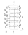
- FIG. 1 is a separated perspective view showing a stem for a semiconductor light emitting device on which the semiconductor light emitting device according to the embodiment of the present invention is mounted.
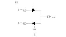
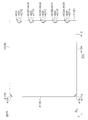
- FIG. 2 is a circuit diagram showing an electrical structure of the stem for a semiconductor light emitting device shown in FIG.
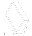
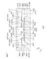
- FIG. 3 is a perspective view of the semiconductor light emitting device shown in FIG.
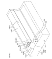
- FIG. 4 is a partially cutaway perspective view of FIG.
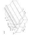
- FIG. 5 is an enlarged perspective view of a part of the region of FIG.
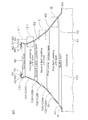
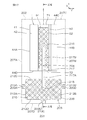
- FIG. 6 is an enlarged cross-sectional view of a part of the semiconductor light emitting device shown in FIG.
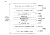
- FIG. 7 is a diagram for explaining a structural example of the light emitting unit layer shown in FIG.
- FIG. 8 is a diagram for explaining a structural example of the tunnel junction layer shown in FIG.
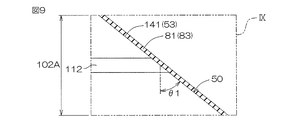
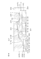
- FIG. 9 is an enlarged view of the region IX shown in FIG.
- FIG. 10 is an enlarged view of the region X shown in FIG.
- FIG. 11 is an enlarged view of the region XI shown in FIG.
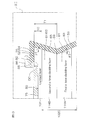
- FIG. 12 is an enlarged view of the region XII shown in FIG. 6, which is an enlarged view showing the structure in which the insulating layer according to the first embodiment is formed.
- FIG. 13 is an enlarged view of the region XII shown in FIG. 6, which is an enlarged view showing the structure in which the insulating layer according to the second embodiment is formed.
- FIG. 14 is an enlarged view of the region XII shown in FIG. 6, which is an enlarged view showing the structure in which the insulating layer according to the third embodiment is formed.
- FIG. 10 is an enlarged view of the region X shown in FIG.
- FIG. 11 is an enlarged view of the region XI shown in FIG.
- FIG. 12 is an enlarged view of the region XII shown in FIG.
- FIG. 15 is an enlarged view of the region XII shown in FIG. 6, which is an enlarged view showing the structure in which the insulating layer according to the fourth embodiment is formed.
- FIG. 16A is a perspective view for explaining an example of a method for manufacturing the semiconductor light emitting device shown in FIG.
- FIG. 16B is a perspective view showing a step after FIG. 16A.
- FIG. 16C is a perspective view showing a step after FIG. 16B.
- FIG. 16D is a perspective view showing a step after FIG. 16C.
- FIG. 16E is a perspective view showing a step after FIG. 16D.
- FIG. 16F is a perspective view showing a step after FIG. 16E.
- FIG. 16G is a perspective view showing a step after FIG. 16F.
- FIG. 16A is a perspective view for explaining an example of a method for manufacturing the semiconductor light emitting device shown in FIG.
- FIG. 16B is a perspective view showing a step after FIG. 16A.
- FIG. 16H is a perspective view showing a step after FIG. 16G.
- FIG. 16I is a perspective view showing a step after FIG. 16H.
- FIG. 16J is a perspective view showing a step after FIG. 16I.
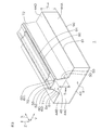
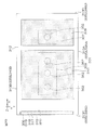
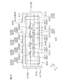
- FIG. 17 is a plan view showing the package according to the first embodiment in which the semiconductor light emitting device shown in FIG. 3 is mounted, through the package body.
- FIG. 18 is a cross-sectional view taken along the line XVIII-XVIII of FIG.
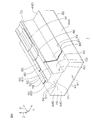
- FIG. 19 is a plan view showing a package according to a second embodiment in which the semiconductor light emitting device shown in FIG. 3 is mounted.
- FIG. 20 is a bottom view of the package shown in FIG. FIG.
- FIG. 21 is a cross-sectional view taken along the line XXI-XXI shown in FIG.
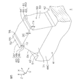
- FIG. 22 is a plan view showing a package according to a third embodiment in which the semiconductor light emitting device shown in FIG. 3 is mounted.
- FIG. 23 is a front view of the package shown in FIG.
- FIG. 24 is a rear view of the package shown in FIG.
- FIG. 25 is a bottom view of the package shown in FIG. 22.
- FIG. 26 is a cross-sectional view taken along the line XXVI-XXVI shown in FIG.
- FIG. 27 is a cross-sectional view taken along the line XXVII-XXVII shown in FIG.
- FIG. 28 is a plan view showing a main part of the housing shown in FIG. 22.
- FIG. 29 is a plan view showing a main part of the housing shown in FIG. 22.
- FIG. 30 is a plan view showing a main part of the housing shown in FIG. 22.
- FIG. 1 is a separated perspective view showing a stem 2 for a semiconductor light emitting device on which the semiconductor light emitting device 1 according to the embodiment of the present invention is mounted.
- the semiconductor light emitting device 1 comprises a semiconductor laser device that generates a laser beam. That is, the stem 2 for the semiconductor light emitting device is a stem for the semiconductor laser device.
- the semiconductor light emitting device stem 2 includes a stem base 3, a first lead terminal 4, a second lead terminal 5, a third lead terminal 6, a first insulator 7, a second insulator 8, and a heat sink. 9.
- the semiconductor light emitting device 1, the photodiode 10, the first lead wire 12, the second lead wire 13, the cap 14, and the closing member 15 are included.
- the stem base 3 includes a plate-shaped member made of metal (for example, iron).
- the stem base 3 is formed in a disk shape in this form.
- the stem base 3 has a first surface 16 on one side, a second surface 17 on the other side, and a side surface 18 connecting the first surface 16 and the second surface 17.
- a plurality of (three in this form) notches are formed at intervals in an arbitrary region on the side surface 18 of the stem base 3.
- the plurality of notches include a first notch 19, a second notch 20, and a third notch 21.
- the first notch 19 is recessed toward the center of the stem base 3.
- the second notch 20 and the third notch 21 are each recessed in a V shape toward the central portion of the stem base 3.
- the second notch 20 and the third notch 21 face each other with the central portion of the stem base 3 interposed therebetween.
- the first notch portion 19, the second notch portion 20, and the third notch portion 21 may indicate the arrangement of the first lead terminal 4, the second lead terminal 5, and the third lead terminal 6.
- the first lead terminal 4, the second lead terminal 5, and the third lead terminal 6 are provided on the second surface 17 of the stem base 3 at intervals from each other.
- the first lead terminal 4, the second lead terminal 5, and the third lead terminal 6 extend in a rod shape, a columnar shape, or a shaft shape along the normal direction of the second surface 17, respectively.
- the first lead terminal 4 is connected to the second surface 17 of the stem base 3. As a result, the first lead terminal 4 is electrically connected to the stem base 3.
- the second lead terminal 5 includes a pull-out portion 22 drawn from the second surface 17 side of the stem base 3 to the first surface 16 side of the stem base 3.
- the lead-out portion 22 of the second lead terminal 5 is pulled out through the first through hole 23 formed in the stem base 3.
- the third lead terminal 6 includes a pull-out portion 24 drawn from the second surface 17 side of the stem base 3 to the first surface 16 side of the stem base 3.
- the lead-out portion 24 of the third lead terminal 6 is pulled out through the second through hole 25 formed in the stem base 3.
- the first insulator 7 is interposed between the second lead terminal 5 and the stem base 3 in the first through hole 23.
- the first insulator 7 electrically insulates the second lead terminal 5 from the stem base 3.
- the first insulator 7 supports the second lead terminal 5.
- the second insulator 8 is interposed between the third lead terminal 6 and the stem base 3 in the second through hole 25.
- the second insulator 8 electrically insulates the third lead terminal 6 from the stem base 3.
- the second insulator 8 supports the third lead terminal 6.
- the heat sink 9 is provided on the first surface 16 of the stem base 3.
- the heat sink 9 includes a block-shaped or plate-shaped member made of silicon, aluminum nitride, or metal (for example, iron).
- the heat sink 9 may be integrally formed with respect to the first surface 16.
- the heat sink 9 may be arranged on the peripheral edge side of the stem base 3 with respect to the central portion of the stem base 3 in a plan view seen from the normal direction of the first surface 16.
- the heat sink 9 has a first mounting surface 26.
- the first mounting surface 26 extends along the normal direction of the first surface 16.
- the first mounting surface 26 is oriented toward the central portion of the stem base 3.
- the semiconductor light emitting device 1 is mounted on the first mounting surface 26 of the heat sink 9. A submount may be interposed between the semiconductor light emitting device 1 and the heat sink 9. The semiconductor light emitting device 1 irradiates the laser beam toward the normal direction of the first surface 16. The semiconductor light emitting device 1 is electrically connected to the first lead terminal 4 via the stem base 3.
- the photodiode 10 is mounted on the first surface 16 of the stem base 3.
- the photodiode 10 is mounted on the first surface 16 in a region facing the heat sink 9 with the central portion of the stem base 3 interposed therebetween.
- the photodiode 10 is mounted in the recess portion 27 formed on the first surface 16.
- the recess portion 27 has a second mounting surface 28 formed on the bottom portion.
- the photodiode 10 is mounted on the second mounting surface 28.
- the photodiode 10 is electrically connected to the first lead terminal 4 via the stem base 3.
- the first lead wire 12 may be a bonding wire.
- the first lead wire 12 electrically connects the semiconductor light emitting device 1 and the second lead terminal 5. Specifically, the first lead wire 12 is connected to the lead-out portion 22 of the second lead terminal 5. As a result, the semiconductor light emitting device 1 is electrically connected to the second lead terminal 5 via the first lead wire 12.
- the second lead wire 13 may be a bonding wire.
- the second lead wire 13 electrically connects the photodiode 10 and the third lead terminal 6. Specifically, the second lead wire 13 is connected to the lead-out portion 24 of the third lead terminal 6. As a result, the photodiode 10 is electrically connected to the third lead terminal 6 via the second lead wire 13.
- the cap 14 includes a tubular member made of metal (for example, iron).
- the cap 14 is mounted on the first surface 16 of the stem base 3.
- the cap 14 accommodates a heat sink 9, a semiconductor light emitting device 1, a photodiode 10, a lead-out portion 22 of the second lead terminal 5, a lead-out portion 24 of the third lead terminal 6, a first lead wire 12, and a second lead wire 13.
- the cap 14 includes an facing wall 29, a side wall 30 and a flange 31.
- the facing wall 29 is formed in a plate shape (in this form, a disk shape).
- the facing wall 29 faces the first surface 16 of the stem base 3.
- the side wall 30 is formed in a tubular shape (cylindrical shape in this form) and is connected to the peripheral edge of the facing wall 29.
- the side wall 30 partitions the opening 32 on the side opposite to the facing wall 29.
- the flange 31 projects at the opening end of the opening 32 on the opposite side of the opening 32.
- the flange 31 is formed in an annular shape (in this form, an annular shape) along the opening end of the opening 32.
- the cap 14 is fixed to the stem base 3 by attaching the flange 31 to the first surface 16.
- a light extraction window 33 is formed on the cap 14.
- the light extraction window 33 is formed on the facing wall 29. The light extraction window 33 guides the laser beam generated by the semiconductor light emitting device 1 from the inside of the cap 14 to the outside of the cap 14.
- the closing member 15 is a member that closes the light extraction window 33.
- the closing member 15 is preferably made of a translucent insulator or a transparent insulator.
- the closing member 15 is made of glass in this form.
- the closing member 15 may be a lens for increasing the directivity of the laser beam. In this form, the closing member 15 closes the light extraction window 33 from the inside of the cap 14.
- the closing member 15 may close the light extraction window 33 from the outside of the cap 14.
- FIG. 2 is a circuit diagram showing the electrical structure of the stem 2 for a semiconductor light emitting device.
- the semiconductor light emitting device 1 has a stem base 3 in such a manner that the cathode is electrically connected to the first lead terminal 4 and the anode is electrically connected to the second lead terminal 5. It is mounted on.
- the photodiode 10 is mounted on the stem base 3 in such a manner that the cathode is electrically connected to the third lead terminal 6 and the anode is electrically connected to the first lead terminal 4.
- the connection mode of the semiconductor light emitting device 1 and the photodiode 10 is arbitrary.
- the semiconductor light emitting device 1 may be mounted in such a manner that the anode is electrically connected to the first lead terminal 4 and the cathode is electrically connected to the second lead terminal 5.
- the photodiode 10 may be mounted in such a manner that the anode is electrically connected to the third lead terminal 6 and the cathode is electrically connected to the first lead terminal 4.
- the stem 2 for a semiconductor light emitting device includes the semiconductor light emitting device 1 and the photodiode 10 .
- a stem 2 for a semiconductor light emitting device that does not include the photodiode 10 may be adopted.
- the third lead terminal 6 may be removed or may be left as an open terminal.
- FIG. 3 is a perspective view of the semiconductor light emitting device 1 shown in FIG.
- FIG. 4 is a partially cutaway perspective view of FIG.
- FIG. 5 is an enlarged perspective view of a part of the region of FIG.
- the semiconductor light emitting device 1 includes a substrate 41 formed in a rectangular parallelepiped shape.
- the substrate 41 is made of an n-type semiconductor substrate containing GaAs (gallium-arsenide).
- the substrate 41 contains at least one of Si (silicon), Te (tellurium), and Se (selenium) as n-type impurities.
- the substrate 41 includes a first main surface 42 on one side, a second main surface 43 on the other side, and substrate side surfaces 44A, 44B, 44C, 44D connecting the first main surface 42 and the second main surface 43.
- the first main surface 42 and the second main surface 43 are formed in a rectangular shape (rectangular shape in this form) in a plan view (hereinafter, simply referred to as “planar view”) viewed from their normal direction Z. There is.
- the substrate side surfaces 44A to 44D include a first substrate side surface 44A, a second substrate side surface 44B, a third substrate side surface 44C, and a fourth substrate side surface 44D.
- the first substrate side surface 44A and the second substrate side surface 44B form a long side of the substrate 41.
- the first substrate side surface 44A and the second substrate side surface 44B extend along the first direction X and face each other in the second direction Y intersecting the first direction X.
- the second direction Y is orthogonal to the first direction X.
- the third substrate side surface 44C and the fourth substrate side surface 44D form a short side of the substrate 41.
- the third substrate side surface 44C and the fourth substrate side surface 44D extend along the second direction Y and face each other in the first direction X. It is preferable that at least the substrate side surface 44C and the substrate side surface 44D of the substrate side surfaces 44A to 44D are mirror-finished. All of the substrate side surfaces 44A to 44D may be mirror-finished.
- the substrate side surfaces 44A to 44D may be cleavage planes.
- the thickness Tsub of the substrate 41 may be 50 ⁇ m or more and 350 ⁇ m or less.
- the thickness Tsub may be 50 ⁇ m or more and 100 ⁇ m or less, 100 ⁇ m or more and 150 ⁇ m or less, 150 ⁇ m or more and 200 ⁇ m or less, 200 ⁇ m or more and 250 ⁇ m or less, 250 ⁇ m or more and 300 ⁇ m or less, or 300 ⁇ m or more and 350 ⁇ m or less.
- the length L1 of the first substrate side surface 44A may be 200 ⁇ m or more and 1000 ⁇ m or less. Even if the length L1 is 200 ⁇ m or more and 300 ⁇ m or less, 300 ⁇ m or more and 400 ⁇ m or less, 400 ⁇ m or more and 500 ⁇ m or less, 500 ⁇ m or more and 600 ⁇ m or less, 600 ⁇ m or more and 700 ⁇ m or less, 700 ⁇ m or more and 800 ⁇ m or less, 800 ⁇ m or more and 900 ⁇ m or less, or 900 ⁇ m or more and 1000 ⁇ m or less. Good.
- the length L2 of the third substrate side surface 44C may be 50 ⁇ m or more and 500 ⁇ m or less.
- the length L2 is 50 ⁇ m or more and 100 ⁇ m or less, 100 ⁇ m or more and 150 ⁇ m or less, 150 ⁇ m or more and 200 ⁇ m or less, 200 ⁇ m or more and 250 ⁇ m or less, 250 ⁇ m or more and 300 ⁇ m or less, 300 ⁇ m or more and 350 ⁇ m or less, 350 ⁇ m or more and 400 ⁇ m or less, 400 ⁇ m or more and 450 ⁇ m or less, or 450 ⁇ m or more and 500 ⁇ m. It may be as follows.
- the semiconductor light emitting device 1 further includes a semiconductor light emitting layer 45.
- the semiconductor light emitting layer 45 is formed on the first main surface 42 of the substrate 41.
- the semiconductor light emitting layer 45 produces light (laser light in this form).
- the semiconductor light emitting layer 45 produces light having a peak wavelength of 800 nm or more and 1000 nm or less. That is, the semiconductor light emitting layer 45 generates light in the infrared region.
- the semiconductor light emitting layer 45 has a mesa structure 50.
- the mesa structure 50 is formed in a plateau shape (ridge shape) protruding from the first main surface 42 toward the side opposite to the second main surface 43.
- the mesa structure 50 is formed at intervals inward from the first substrate side surface 44A and the second substrate side surface 44B. In this form, the mesa structure 50 extends in a band shape along the second direction Y at the central portion of the first main surface 42.
- the thickness Tmesa of the mesa structure 50 may be 1 ⁇ m or more and 40 ⁇ m or less. Even if the thickness Tmesa is 1 ⁇ m or more and 5 ⁇ m or less, 5 ⁇ m or more and 10 ⁇ m or less, 10 ⁇ m or more and 15 ⁇ m or less, 15 ⁇ m or more and 20 ⁇ m or less, 20 ⁇ m or more and 25 ⁇ m or less, 25 ⁇ m or more and 30 ⁇ m or less, 30 ⁇ m or more and 35 ⁇ m or less, or 35 ⁇ m or more and 40 ⁇ m or less. Good.
- the thickness Tmesa is preferably 3 ⁇ m or more and 20 ⁇ m or less.
- the mesa structure 50 includes a base 51, a top 52, a first side wall 53, and a second side wall 54.
- the base 51 is connected to the substrate 41.
- the top 52 has a mesa main surface 55.
- the mesa main surface 55 is formed parallel to the first main surface 42 of the substrate 41.
- the first side wall 53 and the second side wall 54 connect the base 51 and the top 52, respectively.
- the first side wall 53 is a side wall on the side surface 44A of the first substrate.
- the second side wall 54 is a side wall on the side surface 44B side of the second substrate.
- the base 51, the top 52, the first side wall 53, and the second side wall 54 extend in a strip shape along the second direction Y, respectively.
- the peripheral edge of the top 52 is located inward of the peripheral edge of the base 51. That is, the plane area of the region surrounded by the peripheral edge of the top 52 is less than the plane area of the region surrounded by the periphery of the base 51.
- the first side wall 53 and the second side wall 54 are inclined downward from the top 52 toward the base 51.
- the first side wall 53 and the second side wall 54 are inclined downward in such a manner that the angle formed with the normal direction Z of the mesa main surface 55 gradually increases from the top 52 toward the base 51. ing.
- the mesa structure 50 is formed in a tapered shape (square pyramid shape) in which the width along the second direction Y gradually increases from the top 52 side to the base 51 side.
- the first side wall 53 and the second side wall 54 cross the first main surface 42 of the substrate 41.
- the surface layer portion on the first main surface 42 side of the substrate 41 is exposed from the bottom portion of the first side wall 53 and the bottom portion of the second side wall 54.
- a step is formed in a portion of the first main surface 42 of the substrate 41 that connects the inside and outside of the mesa structure 50.
- the portion of the first main surface 42 located inside the mesa structure 50 projects toward the top 52 with respect to the portion of the first main surface 42 located outside the mesa structure 50.
- the portion of the first main surface 42 located outside the mesa structure 50 is recessed toward the second main surface 43 with respect to the portion of the first main surface 42 located inside the mesa structure 50.
- the first main surface 42 of the substrate 41 may be formed flush with each other inside and outside the mesa structure 50.
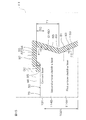
- the mesa structure 50 has a main surface expansion portion 60 that expands the mesa main surface 55.
- the main surface expansion portion 60 includes a first main surface expansion portion 61 and a second main surface expansion portion 62 in this form.
- the first main surface expansion portion 61 is formed at the first corner portion connecting the mesa main surface 55 and the first side wall 53.
- the second main surface extension portion 62 is formed at a second corner portion connecting the main surface 55 of the mesa and the second side wall 54.
- the first main surface expansion portion 61 projects along the tangential direction (second direction Y in this form) from the mesa main surface 55 to the mesa main surface 55 on the surface layer portion of the mesa main surface 55.
- the first main surface expansion portion 61 has a first connection portion 63 connected to the first side wall 53.
- the first main surface expansion portion 61 is formed in an inverted tapered shape that tapers from the first connection portion 63 toward the mesa main surface 55.
- the first main surface expansion portion 61 has a first expansion surface 64 and a first tapered surface 65.
- the first expansion surface 64 is formed flush with the main surface 55 of the mesa and extends the main surface 55 of the mesa.
- the first tapered surface 65 connects the first expansion surface 64 and the first side wall 53 (first connection portion 63).
- the first tapered surface 65 extends in a reverse taper shape from the first connecting portion 63 toward the first expansion surface 64 so as to face the first side wall 53 along the normal direction Z.
- the portion connecting the first expansion surface 64 and the first side wall 53 (the edge of the first main surface expansion portion 61) is located in the area above the first side wall 53.
- the first main surface expansion portion 61 has a first thickness T1 in the normal direction Z.
- the first thickness T1 is the thickness between the first expansion surface 64 and the first connection portion 63 in the normal direction Z.
- the first thickness T1 may be 2000 ⁇ or more and 25000 ⁇ or less.
- the first thickness T1 is 2000 ⁇ or more and 5000 ⁇ or less, 5000 ⁇ or more and 7500 ⁇ or less, 7500 ⁇ or more and 10000 ⁇ or less, 10000 ⁇ or more and 12500 ⁇ or less, 12500 ⁇ or more and 15000 ⁇ or less, 15000 ⁇ or more and 17500 ⁇ or less, 15000 ⁇ or more and 17500 ⁇ or less, 17500 ⁇ or more and 20000 ⁇ or less, 17500 ⁇ or more and 20000 ⁇ or less. It may be more than 25,000 ⁇ or less.
- the first thickness T1 is preferably 5000 ⁇ or more and 15000 ⁇ or less.
- the second main surface expansion portion 62 projects from the mesa main surface 55 to the tangential direction of the mesa main surface 55 (in this form, the second direction Y) in the surface layer portion of the mesa main surface 55.
- the second main surface expansion portion 62 has a second connection portion 66 connected to the second side wall 54.
- the second main surface expansion portion 62 is formed in an inverted tapered shape that tapers from the second connection portion 66 toward the mesa main surface 55.
- the second main surface expansion portion 62 has a second expansion surface 67 and a second tapered surface 68.
- the second expansion surface 67 is formed flush with the main surface 55 of the mesa and extends the main surface 55 of the mesa.
- the second tapered surface 68 connects the second expansion surface 67 and the second side wall 54 (second connection portion 66).
- the second tapered surface 68 extends in a reverse taper shape from the second connecting portion 66 toward the second expansion surface 67 so as to face the second side wall 54 along the normal direction Z.
- the portion connecting the second expansion surface 67 and the second side wall 54 (the edge of the second main surface expansion portion 62) is located in the area above the second side wall 54.
- the second main surface expansion portion 62 has a second thickness T2 in the normal direction Z.
- the second thickness T2 is the thickness between the second expansion surface 67 and the second connection portion 66 in the normal direction Z.
- the second thickness T2 may be 5000 ⁇ or more and 15000 ⁇ or less.
- the second thickness T2 may be 2000 ⁇ or more and 25000 ⁇ or less.
- the second thickness T2 is 2000 ⁇ or more and 5000 ⁇ or less, 5000 ⁇ or more and 7500 ⁇ or less, 7500 ⁇ or more and 10000 ⁇ or less, 10000 ⁇ or more and 12500 ⁇ or less, 12500 ⁇ or more and 15000 ⁇ or less, 15000 ⁇ or more and 17500 ⁇ or less, 15000 ⁇ or more and 17500 ⁇ or less, 17500 ⁇ or more and 20000 ⁇ or less, 17500 ⁇ or more and 20000 ⁇ or less. It may be more than 25,000 ⁇ or less.
- the second thickness T2 is preferably 5000 ⁇ or more and 15000 ⁇ or less.
- the second thickness T2 may exceed the first thickness T1 (T1 ⁇ T2).
- the second thickness T2 may be less than the first thickness T1 (T2 ⁇ T1).
- the mesa structure 50 further includes a first end face 71 and a second end face 72.
- the first end surface 71 is exposed from the third substrate side surface 44C. Specifically, the first end surface 71 is formed flush with respect to the third substrate side surface 44C.
- the first end surface 71 is mirror-finished. In this form, the first end surface 71 forms one cleavage surface with the third substrate side surface 44C.
- the second end surface 72 is exposed from the side surface 44D of the fourth substrate. Specifically, the second end surface 72 is formed flush with respect to the fourth substrate side surface 44D. The second end surface 72 is mirror-finished. In this form, the second end surface 72 forms one cleavage surface with the fourth substrate side surface 44D.
- the first end face 71 and the second end face 72 form a resonator end face.
- the light generated by the semiconductor light emitting layer 45 reciprocates between the first end surface 71 and the second end surface 72, and is amplified by stimulated emission. A part of the amplified light is taken out of the semiconductor light emitting layer 45 as laser light from the first end surface 71 and the second end surface 72.
- the semiconductor light emitting device 1 is mounted on the first mounting surface 26 of the heat sink 9 with either one of the first end surface 71 and the second end surface 72 facing the light extraction window 33 (see FIG. 1).
- the mesa structure 50 includes a contact hole 75 formed in the main surface 55 of the mesa.
- the contact hole 75 is recessed toward the base 51 on the main surface 55 of the mesa.
- the contact holes 75 are formed at intervals inward from the peripheral edge of the main surface 55 of the mesa.
- the contact hole 75 extends in a strip shape along the second direction Y in a plan view.
- the contact hole 75 may communicate with the first end surface 71 and the second end surface 72.
- the contact hole 75 may be formed in a region surrounded by the peripheral edge of the mesa main surface 55 so as not to communicate with the first end surface 71 and the second end surface 72.
- the contact holes 75 are formed at intervals inward from the first connection portion 63 of the first main surface expansion portion 61 in a plan view. It is preferable that the contact holes 75 are formed at intervals inward of the second connecting portion 66 of the second main surface expanding portion 62 in a plan view.
- the depth DC of the contact hole 75 is preferably less than the first thickness T1 (DC ⁇ T1) of the first main surface expansion portion 61.
- the depth DC is preferably not more than half of the first thickness T1 (DC ⁇ T1 / 2).
- the depth DC is more preferably one-third or less (DC ⁇ T1 / 3) of the first thickness T1.
- the depth DC is preferably less than the second thickness T2 (DC ⁇ T2) of the second main surface expansion portion 62.
- the depth DC is preferably not more than half of the second thickness T2 (DC ⁇ T2 / 2).
- the depth DC is more preferably one-third or less (DC ⁇ T2 / 3) of the second thickness T2.
- the depth DC may be 1 ⁇ or more and 2000 ⁇ or less. Depth DC is 1 ⁇ or more and 200 ⁇ or less, 200 ⁇ or more and 400 ⁇ or less, 400 ⁇ or more and 600 ⁇ or less, 600 ⁇ or more and 800 ⁇ or less, 800 ⁇ or more and 1000 ⁇ or less, 1000 ⁇ or more and 1200 ⁇ or less, 1200 ⁇ or more and 1400 ⁇ or less, 1400 ⁇ or more and 1600 ⁇ or less, 1400 ⁇ or more and 1600 ⁇ or less Alternatively, it may be 1800 ⁇ or more and 2000 ⁇ or less.
- the depth DC is preferably 10 ⁇ or more and 1000 ⁇ or less.
- the semiconductor light emitting device 1 further includes an insulating layer 81.
- the insulating layer 81 covers the semiconductor light emitting layer 45.
- the insulating layer 81 is formed in a film shape.
- the insulating layer 81 may contain silicon nitride or silicon oxide.
- the insulating layer 81 contains silicon nitride in this form.
- the insulating layer 81 covers the top 52 and the first side wall 53 of the mesa structure 50 via the first main surface expansion portion 61.
- the insulating layer 81 covers the top portion 52 and the second side wall 54 of the mesa structure 50 via the second main surface expansion portion 62.
- the insulating layer 81 integrally includes the top coating portion 82, the side wall coating portion 83, and the substrate coating portion 84.
- the top covering portion 82 covers the top 52 of the mesa structure 50.
- the side wall covering portion 83 covers the first side wall 53 and the second side wall 54 of the mesa structure 50.
- the substrate covering portion 84 covers the first main surface 42 of the substrate 41.
- the first main surface expansion portion 61 and the second main surface expansion portion 62 are covered with a top covering portion 82 and a side wall covering portion 83.
- a contact opening 85 is formed in the insulating layer 81.
- the contact opening 85 is formed in the top covering portion 82 so as to communicate with the contact hole 75.
- the contact opening 85 exposes the inner wall of the contact hole 75.
- the inner wall of the contact opening 85 extends along the inner wall of the contact hole 75.
- the semiconductor light emitting device 1 further includes a contact electrode 86.
- the contact electrode 86 is electrically connected to the semiconductor light emitting layer 45 in the contact hole 75.
- the contact electrode 86 is formed in a film shape.
- the contact electrode 86 covers the inner wall of the contact hole 75 and is drawn out onto the insulating layer 81 through the contact opening 85.
- the contact electrode 86 covers the top 52 of the mesa structure 50 and exposes the first side wall 53 and the second side wall 54 of the mesa structure 50. In this form, the contact electrode 86 is formed only in the region surrounded by the peripheral edge of the apex 52 including the first main surface expansion portion 61 and the second main surface expansion portion 62.
- the contact electrode 86 may cover either or both of the first main surface expansion portion 61 and the second main surface expansion portion 62.
- the contact electrode 86 may expose either or both of the first main surface expansion portion 61 and the second main surface expansion portion 62.
- the contact electrode 86 may cover the first side wall 53 and the second side wall 54 of the mesa structure 50 from the top portion 52 via the first main surface expansion portion 61 and the second main surface expansion portion 62.
- the contact electrode 86 may have a laminated structure in which a plurality of electrode layers are laminated.
- the contact electrode 86 may include a first electrode layer and a second electrode layer laminated in this order from the semiconductor light emitting layer 45 side.
- the first electrode layer may be a barrier electrode layer containing at least one of a Ti (titanium) layer and a TiN (titanium nitride) layer.
- the thickness of the first electrode layer may be 200 ⁇ or more and 2000 ⁇ or less.
- the second electrode layer may be a low resistance electrode layer including an Au (gold) layer.
- the low resistance electrode layer may be a seed layer.
- the thickness of the second electrode layer may be 1000 ⁇ or more and 3000 ⁇ or less.
- the semiconductor light emitting device 1 further includes a first terminal electrode 91 and a second terminal electrode 92.
- the first terminal electrode 91 is formed on the contact electrode 86.
- the first terminal electrode 91 is electrically connected to the semiconductor light emitting layer 45 via the contact electrode 86.
- the first terminal electrode 91 covers the top 52 of the mesa structure 50 with the contact electrode 86 sandwiched therein, and exposes the first side wall 53 and the second side wall 54 of the mesa structure 50.
- the first terminal electrode 91 is formed only in the region surrounded by the peripheral edge of the top portion 52 including the first main surface expansion portion 61 and the second main surface expansion portion 62.
- the first terminal electrode 91 may cover either or both of the first main surface expansion portion 61 and the second main surface expansion portion 62.
- the first terminal electrode 91 may expose either or both of the first main surface expansion portion 61 and the second main surface expansion portion 62.
- the first terminal electrode 91 may cover the first side wall 53 and the second side wall 54 of the mesa structure 50 from the top portion 52 via the first main surface expansion portion 61 and the second main surface expansion portion 62.
- the first terminal electrode 91 has a single layer structure composed of a single electrode layer.
- the first terminal electrode 91 may include an Au (gold) layer.
- the first terminal electrode 91 may be an Au (gold) plating layer.
- the second terminal electrode 92 is formed on the second main surface 43 of the substrate 41. In this form, the second terminal electrode 92 covers the entire surface of the second main surface 43. The second terminal electrode 92 may be formed on the second main surface 43 so as to expose the peripheral edge portion of the second main surface 43. The second terminal electrode 92 may have a laminated structure including a plurality of electrode layers.
- the second terminal electrode 92 may include at least one of a Ni (nickel) layer, an AuGe (gold-germanium alloy) layer, a Ti (titanium) layer and an Au (gold) layer.
- the second terminal electrode 92 may have a laminated structure in which at least two of the Ni layer, the AuGe layer, the Ti layer, and the Au layer are laminated in any manner.
- the second terminal electrode 92 may include a Ni layer, an AuGe layer, a Ti layer, and an Au layer laminated in this order from the second main surface 43 side.
- the second terminal electrode 92 is connected to the first lead terminal 4 via the first lead wire 12 (see FIG. 1).
- the first terminal electrode 91 is connected to the first lead terminal 4 via the first lead wire 12
- the second terminal electrode 92 is connected to the heat sink 9 (see FIG. 1).
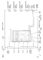
- FIG. 6 is an enlarged cross-sectional view of a part of the semiconductor light emitting device 1 shown in FIG.
- FIG. 7 is a diagram for explaining a structural example of the light emitting unit layer 102 shown in FIG.
- FIG. 8 is a diagram for explaining a structural example of the tunnel junction layer 103 shown in FIG.
- the semiconductor light emitting layer 45 includes an n-type buffer layer 101 laminated on the first main surface 42 of the substrate 41 in this form.
- the n-type buffer layer 101 contains GaAs (gallium-arsenide).
- the n-type buffer layer 101 contains at least one of Si (silicon), Te (tellurium), and Se (selenium) as n-type impurities.
- the concentration of n-type impurities in the n-type buffer layer 101 may be 1 ⁇ 10 18 cm -3 or more and 1 ⁇ 10 19 cm -3 or less.
- the semiconductor light emitting layer 45 includes a light emitting unit layer 102 laminated on the n-type buffer layer 101.
- the light emitting unit layer 102 generates light by combining holes and electrons.
- the semiconductor light emitting layer 45 includes a plurality of (three in this form) light emitting unit layers 102.
- the plurality of light emitting unit layers 102 include a first light emitting unit layer 102A, a second light emitting unit layer 102B, and a third light emitting unit layer 102C stacked in this order from the n-type buffer layer 101 side.
- the semiconductor light emitting layer 45 further includes a tunnel junction layer 103 interposed in a region between a plurality of light emitting unit layers 102A to 102C adjacent to each other.
- the tunnel junction layer 103 generates a tunnel current due to the tunnel effect and supplies it to the light emitting unit layers 102A to 102C.
- the tunnel junction layer 103 includes a plurality of (two in this form) tunnel junction layers 103.
- the plurality of tunnel junction layers 103 include a first tunnel junction layer 103A and a second tunnel junction layer 103B.
- the first tunnel junction layer 103A is interposed in the region between the first light emitting unit layer 102A and the second light emitting unit layer 102B.
- the second tunnel junction layer 103B is interposed in the region between the second light emitting unit layer 102B and the third light emitting unit layer 102C.
- the first light emitting unit layer 102A, the second light emitting unit layer 102B, and the third light emitting unit layer 102C are n-type clad layer 110 (first semiconductor layer) laminated in this order from the substrate 41 side. It has a laminated structure including a first guide layer 111, an active layer 112, a second guide layer 113, and a p-type clad layer 114 (second semiconductor layer), respectively.
- the n-type clad layer 110 contains AlGaAs (aluminum-gallium-arsenide).
- the n-type clad layer 110 contains at least one of Si (silicon), Te (tellurium), and Se (selenium) as n-type impurities.
- the concentration of n-type impurities in the n-type clad layer 110 may be 1 ⁇ 10 17 cm -3 or more and 1 ⁇ 10 19 cm -3 or less.
- the n-type clad layer 110 includes a first n-type clad layer 110A and a second n-type clad layer 110B laminated in this order from the substrate 41 side.
- the first n-type clad layer 110A contains Al A Ga (1-A) As having a first Al composition A.
- the first Al composition A may be 0.4 or more and 0.6 or less.
- the first Al composition A may be 0.4 or more and 0.45 or less, 0.45 or more and 0.5 or less, 0.5 or more and 0.55 or less, or 0.55 or more and 0.6 or less.
- the concentration of n-type impurities in the first n-type clad layer 110A may be 5 ⁇ 10 17 cm -3 or more and 1 ⁇ 10 19 cm -3 or less.
- the thickness of the 1n type clad layer 110A may be 5000 ⁇ or more and 10000 ⁇ or less.
- the thickness of the 1n type clad layer 110A may be 5000 ⁇ or more and 6000 ⁇ or less, 6000 ⁇ or more and 7000 ⁇ or less, 7000 ⁇ or more and 8000 ⁇ or less, 8000 ⁇ or more and 9000 ⁇ or less, or 9000 ⁇ or more and 10000 ⁇ or less.
- the second n-type clad layer 110B contains Al B Ga (1-B) As having a second Al composition B different from the first Al composition A of the first n-type clad layer 110A. Specifically, the second Al composition B is less than the first Al composition A (B ⁇ A).
- the second Al composition B may be 0.2 or more and 0.4 or less.
- the second Al composition B may be 0.2 or more and 0.25 or less, 0.25 or more and 0.3 or less, 0.3 or more and 0.35 or less, or 0.35 or more and 0.4 or less.
- the second n-type clad layer 110B has an n-type impurity concentration different from the n-type impurity concentration of the first n-type clad layer 110A. Specifically, the n-type impurity concentration of the second n-type clad layer 110B is less than the n-type impurity concentration of the first n-type clad layer 110A.
- the n-type impurity concentration of the second n-type clad layer 110B may be 1 ⁇ 10 17 cm -3 or more and 5 ⁇ 10 18 cm -3 or less.
- the second n-type clad layer 110B may have a thickness different from the thickness of the first n-type clad layer 110A.
- the second n-type clad layer 110B may have a thickness exceeding the thickness of the first n-type clad layer 110A.
- the thickness of the second n-type clad layer 110B may be 7,000 ⁇ or more and 13000 ⁇ or less.
- the thickness of the second n-type clad layer 110B may be 7000 ⁇ or more and 8000 ⁇ or less, 8000 ⁇ or more and 9000 ⁇ or less, 9000 ⁇ or more and 10000 ⁇ or less, 10000 ⁇ or more and 11000 ⁇ or less, 11000 ⁇ or more and 12000 ⁇ or less, or 12000 ⁇ or more and 13000 ⁇ or less.
- the first guide layer 111 contains Al C Ga (1-C) As having a third Al composition C different from the Al composition (first Al composition A and second Al composition B) of the n-type clad layer 110. Specifically, the third Al composition C is less than the Al composition (C ⁇ B ⁇ A) of the n-type clad layer 110.
- the third Al composition C may be more than 0 and 0.2 or less.
- the third Al composition C may be more than 0 and 0.05 or less, 0.05 or more and 0.1 or less, 0.1 or more and 0.15 or less, or 0.15 or more and 0.2 or less.
- the first guide layer 111 may be free of impurities.
- the thickness of the first guide layer 111 may be 50 ⁇ or more and 250 ⁇ or less.
- the thickness of the first guide layer 111 may be 50 ⁇ or more and 100 ⁇ or less, 100 ⁇ or more and 150 ⁇ or less, 150 ⁇ or more and 200 ⁇ or less, or 200 ⁇ or more and 250 ⁇ or less.
- the active layer 112 has a multiple quantum well structure including a well layer 115 and a barrier layer 116.
- the active layer 112 has a three-layer structure including a well layer 115, a barrier layer 116, and a well layer 115 laminated in this order from the substrate 41 side.
- the active layer 112 may have a multiple quantum well structure including well layers 115 and barrier layers 116 that are alternately laminated over a plurality of cycles (two or more cycles).
- the lowermost layer of the active layer 112 with respect to the substrate 41 side may be the well layer 115 or the barrier layer 116.
- the uppermost layer of the active layer 112 may be a well layer 115 or a barrier layer 116.
- the well layer 115 contains In ⁇ Ga (1- ⁇ ) As having an In composition ⁇ .
- the In composition ⁇ may be more than 0 and 0.2 or less.
- the In composition ⁇ may be more than 0 and 0.05 or less, 0.05 or more and 0.1 or less, 0.1 or more and 0.15 or less, or 0.15 or more and 0.2 or less.
- the well layer 115 may be free of impurities.
- the thickness of the well layer 115 may be less than the thickness of the first guide layer 111.
- the thickness of the well layer 115 may be 10 ⁇ or more and 150 ⁇ or less.
- the thickness of the well layer 115 may be 10 ⁇ or more and 50 ⁇ or less, 50 ⁇ or more and 100 ⁇ or less, or 100 ⁇ or more and 150 ⁇ or less.
- the barrier layer 116 contains Al D Ga (1-D) As having a fourth Al composition D different from the Al composition (first Al composition A and second Al composition B) of the n-type clad layer 110. Specifically, the fourth Al composition D is less than the Al composition (D ⁇ B ⁇ A) of the n-type clad layer 110.
- the fourth Al composition D may be more than 0 and 0.2 or less.
- the fourth Al composition D may be more than 0 and 0.05 or less, 0.05 or more and 0.1 or less, 0.1 or more and 0.15 or less, or 0.15 or more and 0.2 or less.
- the barrier layer 116 may be free of impurities.
- the barrier layer 116 may have a thickness different from that of the well layer 115.
- the thickness of the barrier layer 116 may exceed the thickness of the well layer 115 and be less than the thickness of the first guide layer 111.
- the thickness of the barrier layer 116 may be 20 ⁇ or more and 200 ⁇ or less.
- the thickness of the first guide layer 111 may be 20 ⁇ or more and 50 ⁇ or less, 50 ⁇ or more and 100 ⁇ or less, 100 ⁇ or more and 150 ⁇ or less, or 150 ⁇ or more and 200 ⁇ or less.
- the second guide layer 113 contains Al E Ga (1-E) As having a fifth Al composition E different from the Al composition (first Al composition A and second Al composition B) of the n-type clad layer 110. Specifically, the fifth Al composition E is less than the Al composition (E ⁇ B ⁇ A) of the n-type clad layer 110.
- the fifth Al composition E may be more than 0 and 0.2 or less.
- the fifth Al composition E may be more than 0 and 0.05 or less, 0.05 or more and 0.1 or less, 0.1 or more and 0.15 or less, or 0.15 or more and 0.2 or less.
- the second guide layer 113 may be free of impurities.
- the thickness of the second guide layer 113 may exceed the thickness of the barrier layer 116.
- the thickness of the second guide layer 113 may be 50 ⁇ or more and 250 ⁇ or less.
- the thickness of the second guide layer 113 may be 50 ⁇ or more and 100 ⁇ or less, 100 ⁇ or more and 150 ⁇ or less, 150 ⁇ or more and 200 ⁇ or less, or 200 ⁇ or more and 250 ⁇ or less.
- the p-type clad layer 114 contains AlGaAs.
- the p-type clad layer 114 contains C (carbon) as a p-type impurity.
- the p-type impurity concentration of the p-type clad layer 114 may be 1 ⁇ 10 17 cm -3 or more and 1 ⁇ 10 19 cm -3 or less.
- the p-type clad layer 114 includes a first p-type clad layer 114A and a second p-type clad layer 114B laminated in this order from the substrate 41 side.
- the first p-type clad layer 114A contains Al F Ga (1-F) As having a sixth Al composition F.
- the sixth Al composition F may be 0.2 or more and 0.4 or less.
- the sixth Al composition F may be 0.2 or more and 0.25 or less, 0.25 or more and 0.3 or less, 0.3 or more and 0.35 or less, or 0.35 or more and 0.4 or less.
- the p-type impurity concentration of the first p-type clad layer 114A may be 1 ⁇ 10 17 cm -3 or more and 5 ⁇ 10 18 cm -3 or less.
- the thickness of the first p-type clad layer 114A may be 8000 ⁇ or more and 15000 ⁇ or less.
- the thickness of the 1st p-type clad layer 114A is 8000 ⁇ or more and 9000 ⁇ or less, 9000 ⁇ or more and 10000 ⁇ or less, 10000 ⁇ or more and 11000 ⁇ or less, 11000 ⁇ or more and 12000 ⁇ or less, 12000 ⁇ or more and 13000 ⁇ or less, 13000 ⁇ or more and 14000 ⁇ or less, or 14000 ⁇ or more. May be good.
- the second p-type clad layer 114B contains Al G Ga (1-G) As having a seventh Al composition G different from the sixth Al composition F of the first p-type clad layer 114A. Specifically, the 7th Al composition G exceeds the 6th Al composition F (F ⁇ G).
- the seventh Al composition G may be 0.4 or more and 0.6 or less.
- the seventh Al composition G may be 0.4 or more and 0.45 or less, 0.45 or more and 0.5 or less, 0.5 or more and 0.55 or less, or 0.55 or more and 0.6 or less.
- the second p-type clad layer 114B has a p-type impurity concentration different from the p-type impurity concentration of the first p-type clad layer 114A. Specifically, the p-type impurity concentration of the second p-type clad layer 114B exceeds the p-type impurity concentration of the first p-type clad layer 114A.
- the p-type impurity concentration of the second p-type clad layer 114B may be 5 ⁇ 10 17 cm -3 or more and 1 ⁇ 10 19 cm -3 or less.
- the second p-type clad layer 114B may have a thickness different from the thickness of the first p-type clad layer 114A.
- the second p-type clad layer 114B may have a thickness less than the thickness of the first p-type clad layer 114A.
- the thickness of the second p-type clad layer 114B may be 4000 ⁇ or more and 10000 ⁇ or less.
- the thickness of the second p-type clad layer 114B may be 4000 ⁇ or more and 5000 ⁇ or less, 5000 ⁇ or more and 6000 ⁇ or less, 6000 ⁇ or more and 7000 ⁇ or less, 7000 ⁇ or more and 8000 ⁇ or less, 8000 ⁇ or more and 9000 ⁇ or less, or 9000 ⁇ or more and 10000 ⁇ or less.
- the first tunnel junction layer 103A and the second tunnel junction layer 103B have a p-type tunnel junction layer 121 and an n-type tunnel junction layer 122 laminated in this order from the substrate 41 side, respectively. ..
- the tunnel junction layer 103 has a plurality of light emission in such a manner that the p-type tunnel junction layer 121 is electrically connected to the p-type clad layer 114 and the n-type tunnel junction layer 122 is electrically connected to the n-type clad layer 110. It is interposed in the region between the unit layers 102A to 102C.
- the p-type tunnel junction layer 121 contains GaAs.
- the p-type tunnel junction layer 121 contains C (carbon) as a p-type impurity.
- the p-type tunnel junction layer 121 has a p-type impurity concentration different from the p-type impurity concentration of the p-type clad layer 114. Specifically, the p-type impurity concentration of the p-type tunnel junction layer 121 exceeds the p-type impurity concentration of the p-type clad layer 114.
- the concentration of p-type impurities in the p-type tunnel junction layer 121 may be 1 ⁇ 10 18 cm -3 or more and 1 ⁇ 10 20 cm -3 or less.
- the thickness of the p-type tunnel junction layer 121 may be 100 ⁇ or more and 1000 ⁇ or less.
- the thickness of the p-type tunnel junction layer 121 may be 100 ⁇ or more and 200 ⁇ or less, 200 ⁇ or more and 400 ⁇ or less, 400 ⁇ or more and 600 ⁇ or less, 600 ⁇ or more and 800 ⁇ or less, or 800 ⁇ or more and 1000 ⁇ or less.
- the n-type tunnel junction layer 122 contains GaAs.
- the n-type tunnel junction layer 122 contains at least one of Si (silicon), Te (tellurium), and Se (selenium) as n-type impurities.
- the n-type tunnel junction layer 122 has an n-type impurity concentration different from the n-type impurity concentration of the n-type clad layer 110. Specifically, the n-type impurity concentration of the n-type tunnel junction layer 122 exceeds the n-type impurity concentration of the n-type clad layer 110.
- the concentration of n-type impurities in the n-type tunnel junction layer 122 may be 5 ⁇ 10 17 cm -3 or more and 5 ⁇ 10 19 cm -3 or less.
- the thickness of the n-type tunnel junction layer 122 may be 100 ⁇ or more and 1000 ⁇ or less.
- the thickness of the n-type tunnel junction layer 122 may be 100 ⁇ or more and 200 ⁇ or less, 200 ⁇ or more and 400 ⁇ or less, 400 ⁇ or more and 600 ⁇ or less, 600 ⁇ or more and 800 ⁇ or less, or 800 ⁇ or more and 1000 ⁇ or less.
- a p-type contact layer 131 is formed on the third light emitting unit layer 102C.
- the p-type contact layer 131 contains GaAs.
- the p-type contact layer 131 contains C (carbon) as a p-type impurity.
- the p-type contact layer 131 has a p-type impurity concentration different from the p-type impurity concentration of the p-type clad layer 114. Specifically, the p-type impurity concentration of the p-type contact layer 131 exceeds the p-type impurity concentration of the p-type clad layer 114.
- the p-type contact layer 131 of the p-type contact layer 131 may be 5 ⁇ 10 18 cm -3 or more and 1 ⁇ 10 20 cm -3 or less.
- the thickness TC of the p-type contact layer 131 may be 1000 ⁇ or more and 5000 ⁇ or less.
- the thickness TC of the p-type contact layer 131 may be 1000 ⁇ or more and 2000 ⁇ or less, 2000 ⁇ or more and 3000 ⁇ or less, 3000 ⁇ or more and 4000 ⁇ or less, or 4000 ⁇ or more and 5000 ⁇ or less.
- the semiconductor light emitting layer 45 has an n-type buffer layer 101, a first light emitting unit layer 102A, a first tunnel junction layer 103A, a second light emitting unit layer 102B, a second tunnel junction layer 103B, and a third. It has a mesa structure 50 including a light emitting unit layer 102C and a p-type contact layer 131.
- the base 51 of the mesa structure 50 includes an n-type buffer layer 101.
- the base portion 51 also includes a surface layer portion of the first main surface 42 of the substrate 41.
- the top 52 of the mesa structure 50 includes a p-type contact layer 131.
- the first side wall 53 and the second side wall 54 of the mesa structure 50 are an n-type buffer layer 101, a first light emitting unit layer 102A, a first tunnel junction layer 103A, a second light emitting unit layer 102B, a second tunnel junction layer 103B, and a second. 3
- the light emitting unit layer 102C and the p-type contact layer 131 are included, respectively.
- the first side wall 53 and the second side wall 54 also include a surface layer portion of the first main surface 42 of the substrate 41 in this form.
- FIG. 9 is an enlarged view of the region IX shown in FIG.
- FIG. 10 is an enlarged view of the region X shown in FIG.
- FIG. 11 is an enlarged view of the region XI shown in FIG.
- FIG. 12 is an enlarged view of the region XII shown in FIG.
- the first terminal electrode 91 is not shown.
- the first side wall 53 and the second side wall 54 of the mesa structure 50 include a first part 141, a second part 142, and a third part 143, respectively.
- the first portion 141 is a portion where the first light emitting unit layer 102A is exposed.
- the second portion 142 is a portion where the second light emitting unit layer 102B is exposed.
- the third portion 143 is a portion where the third light emitting unit layer 102C is exposed.
- the structure of the mesa structure 50 on the second side wall 54 side is the same as the structure on the first side wall 53 side. In the following, the structure on the first side wall 53 side will be described as an example, and the description of the structure on the second side wall 54 side will be omitted.
- the first angle ⁇ 1 of the first portion 141 is 45 ° or more and 75 ° or less.
- the first angle ⁇ 1 is an angle formed by the first portion 141 in the mesa structure 50 with respect to the normal direction Z.
- the first portion 141 may gradually increase from the top 52 side toward the base 51 side in the range of the first angle ⁇ 1.
- the first angle ⁇ 1 may be measured with reference to the active layer 112 of the first light emitting unit layer 102A.
- the second angle ⁇ 2 of the second portion 142 is less than the first angle ⁇ 1 of the first portion 141 ( ⁇ 2 ⁇ 1).
- the second angle ⁇ 2 is an angle formed by the second portion 142 in the mesa structure 50 with respect to the normal direction Z.
- the second angle ⁇ 2 is 30 ° or more and 50 ° or less under the condition that the first angle is less than ⁇ 1.
- the second portion 142 may gradually increase from the top 52 side toward the base 51 side in the range of the second angle ⁇ 2.
- the second angle ⁇ 2 may be measured with reference to the active layer 112 of the second light emitting unit layer 102B.
- the third angle ⁇ 3 of the third portion 143 is less than the second angle ⁇ 2 of the second portion 142 ( ⁇ 3 ⁇ 2 ⁇ 1).
- the third angle ⁇ 3 is an angle formed by the third portion 143 in the mesa structure 50 with respect to the normal direction Z.
- the third angle ⁇ 3 is 20 ° or more and 45 ° or less under the condition that the second angle is less than ⁇ 2.
- the third portion 143 may gradually increase from the top 52 side toward the base 51 side in the range of the third angle ⁇ 3.
- the third angle ⁇ 3 may be measured with reference to the active layer 112 of the third light emitting unit layer 102C.
- the first main surface expansion portion 61 includes a p-type contact layer 131. Specifically, the first main surface expansion portion 61 includes a part of the p-type contact layer 131 and the third light emitting unit layer 102C. A part of the third light emitting unit layer 102C is a p-type clad layer 114 in this form. More specifically, a part of the third light emitting unit layer 102C is a second p-type clad layer 114B.
- the first connection portion 63 of the first main surface expansion portion 61 is formed in the region on the top 52 side in the first side wall 53 of the mesa structure 50.
- the first connecting portion 63 is formed at a boundary portion (near the boundary) between the first p-type clad layer 114A and the second p-type clad layer 114B. That is, the first tapered surface 65 is bent starting from the boundary portion (near the boundary) between the first p-type clad layer 114A and the second p-type clad layer 114B, and faces the first side wall 53 along the normal direction Z. It is tilted in the direction of Of course, the first connecting portion 63 may be formed on the first p-type clad layer 114A or the second p-type clad layer 114B.
- the taper angle ⁇ T of the first tapered surface 65 is a negative value.
- the taper angle ⁇ T is an angle formed by the first tapered surface 65 in the mesa structure 50 with respect to the normal direction Z.
- of the taper angle ⁇ T is less than the absolute value
- the taper angle ⁇ T may be ⁇ 25 ° or more and ⁇ 10 ° or less.
- the taper angle ⁇ T may be ⁇ 25 ° or more and ⁇ 20 ° or less, ⁇ 20 ° or more and ⁇ 15 ° or less, or ⁇ 15 ° or more and ⁇ 10 ° or less.
- the contact hole 75 is formed in the p-type contact layer 131.
- the depth DC of the contact hole 75 is less than the thickness TC of the p-type contact layer 131 (DC ⁇ TC).
- the p-type contact layer 131 is exposed from the entire inner wall of the contact hole 75.
- the top covering portion 82 of the insulating layer 81 has an overhang portion 82A protruding into the contact hole 75 so as to face the bottom wall of the contact hole 75.
- the contact opening 85 is formed in the overhang portion 82A.
- the inner wall of the contact opening 85 is located inside the side wall of the contact hole 75.
- the inner wall of the contact opening 85 is, in this form, located within the area surrounded by the side walls of the contact hole 75 in plan view.
- a recess 151 is formed in the region between the overhang portion 82A and the contact hole 75.
- the contact electrode 86 enters the recess 151 in the contact hole 75 and is connected to the side wall and the bottom wall of the contact hole 75.
- the insulating layer 81 may have the form shown in FIG.
- FIG. 13 is an enlarged view of the region XII shown in FIG. 6, which is an enlarged view showing a structure in which the insulating layer 81 according to the second embodiment is formed.
- the first terminal electrode 91 is not shown.
- the insulating layer 81 according to the first embodiment had an overhang portion 82A.
- the insulating layer 81 according to the second embodiment does not have the overhang portion 82A.
- the inner wall of the contact opening 85 may be formed flush with respect to the side wall of the contact hole 75, as shown in FIG.
- the insulating layer 81 may have the form shown in FIG.
- FIG. 14 is an enlarged view of the region XII shown in FIG. 6, which is an enlarged view showing a structure in which the insulating layer 81 according to the third embodiment is formed.
- the first terminal electrode 91 is not shown.
- the insulating layer 81 according to the first embodiment had an overhang portion 82A.
- the insulating layer 81 according to the third embodiment does not have the overhang portion 82A.
- the inner wall of the contact opening 85 may be located in the outer region of the mesa structure 50 with respect to the side wall of the contact hole 75, as shown in FIG.
- the contact opening 85 may expose a part of the mesa main surface 55 of the mesa structure 50 in addition to the contact hole 75.
- the contact electrode 86 is connected to the side wall and bottom wall of the contact hole 75 and the mesa main surface 55 of the mesa structure 50 in the contact hole 75 and the contact opening 85.
- the insulating layer 81 may have the form shown in FIG.
- FIG. 15 is an enlarged view of the region XII shown in FIG. 6, which is an enlarged view showing a structure in which the insulating layer 81 according to the fourth embodiment is formed.
- the first terminal electrode 91 is not shown.
- the insulating layer 81 according to the first embodiment had an overhang portion 82A.
- the insulating layer 81 according to the third embodiment does not have the overhang portion 82A.
- the insulating layer 81 (top covering portion 82) may cover the side wall and the bottom wall of the contact hole 75 as shown in FIG.
- the inner wall of the contact opening 85 may be located in the contact hole 75. That is, the contact opening 85 may expose the bottom wall of the contact hole 75 in the contact hole 75. In this case, the contact electrode 86 is connected to the bottom wall of the contact hole 75 within the contact opening 85.
- FIG. 16A to 16J are perspective views for explaining an example of the manufacturing method of the semiconductor light emitting device 1 shown in FIG. 16A to 16J show a region in which one semiconductor light emitting device 1 is formed.
- the wafer 161 that is the base of the substrate 41 is prepared.
- the wafer 161 has a first wafer main surface 162 and a second wafer main surface 163.
- the first wafer main surface 162 and the second wafer main surface 163 correspond to the first main surface 42 and the second main surface 43 of the substrate 41, respectively.
- a plurality of device forming regions 164 are set on the first wafer main surface 162.
- the plurality of device forming regions 164 are regions in which the semiconductor light emitting device 1 is formed.
- the semiconductor laminated structure 165 which is the base of the semiconductor light emitting layer 45 (mesa structure 50), is formed on the first wafer main surface 162.
- the semiconductor laminated structure 165 includes an n-type buffer layer 101, a first light emitting unit layer 102A, a first tunnel junction layer 103A, a second light emitting unit layer 102B, and a second tunnel junction laminated in this order from the first wafer main surface 162 side. It includes a layer 103B, a third light emitting unit layer 102C, and a p-type contact layer 131.
- the semiconductor laminated structure 165 is formed by an epitaxial growth method.
- the semiconductor light emitting layer 45 (mesa structure 50) is formed.
- a mask 166 having a predetermined pattern is formed on the semiconductor laminated structure 165.
- the mask 166 may be a resin resist film.
- the mask 166 has an opening 166a that covers the region where the mesa structure 50 should be formed and exposes the other regions.
- the unnecessary portion of the semiconductor laminated structure 165 is removed by an etching method via a mask 166.
- the etching method is preferably a wet etching method.
- the semiconductor light emitting layer 45 (mesa structure 50) is formed.
- the processing conditions of the wet etching method are adjusted to form the mesa structure 50 having the main surface expansion portion 60.
- the mask 166 is removed.
- the insulating layer 81 is formed on the first wafer main surface 162 so as to cover the semiconductor light emitting layer 45 (mesa structure 50).
- the insulating layer 81 may be formed by a CVD (Chemical Vapor Deposition) method.
- the contact opening 85 is formed in the insulating layer 81.
- a mask 167 having a predetermined pattern is formed on the first wafer main surface 162 so as to cover the semiconductor light emitting layer 45 (mesa structure 50).
- the mask 167 may be a resin resist film.
- the mask 167 has an opening 167a that exposes the area where the contact hole 75 should be formed.
- the unnecessary portion of the insulating layer 81 is removed by an etching method via a mask 167.
- the etching method may be a dry etching method or a wet etching method.
- the contact opening 85 is formed in the insulating layer 81.
- the mask 167 is removed.
- a contact hole 75 is formed in the mesa main surface 55 of the mesa structure 50.
- a portion exposed from the contact opening 85 on the main surface 55 of the mesa is removed by an etching method using the insulating layer 81 as a mask.
- the etching method may be a dry etching method or a wet etching method.
- the contact hole 75 is formed on the mesa main surface 55 of the mesa structure 50.
- the base contact electrode 168 which is the base of the contact electrode 86, is formed on the first wafer main surface 162 so as to cover the semiconductor light emitting layer 45 (mesa structure 50).
- the base contact electrode 168 may have a laminated structure including a first electrode layer including a Ti layer and / or a TiN layer, and a second electrode layer including an Au layer.
- the base contact electrode 168 may be formed by a sputtering method.
- a mask 169 having a predetermined pattern is formed on the base contact electrode 168.
- the mask 169 may be a resin resist film.
- the mask 169 has an opening 169a that exposes a region of the base contact electrode 168 other than the region where the contact electrode 86 should be formed.
- an unnecessary portion of the base contact electrode 168 is removed by an etching method via a mask 169.
- the etching method may be a dry etching method or a wet etching method.
- the contact electrode 86 is formed on the mesa main surface 55 of the mesa structure 50.
- the first terminal electrode 91 is formed on the contact electrode 86, and the second terminal electrode 92 is formed on the second wafer main surface 163.
- the first terminal electrode 91 may include an Au layer.
- the first terminal electrode 91 may be formed by a gold plating method.
- the second terminal electrode 92 may include at least one of a Ni layer, an AuGe layer, a Ti layer, and an Au layer.
- the second terminal electrode 92 may be formed by a sputtering method.
- the wafer 161 is cut (cleavage) along the plurality of device forming regions 164.
- the plurality of semiconductor light emitting devices 1 are cut out from one wafer 161.
- the semiconductor light emitting device 1 is manufactured through the steps including the above.
- FIGS. 16A to 16J an example in which the forming step of the insulating layer 81 (see FIG. 16D) was carried out prior to the forming step of the contact hole 75 (see FIG. 16F) was described.
- the step of forming the contact hole 75 may be carried out prior to the step of forming the insulating layer 81.
- the contact hole 75 is formed by using a mask having a predetermined pattern instead of the insulating layer 81.
- the main surface of the mesa structure 50 is expanded by the first main surface expansion portion 61 and the second main surface expansion portion 62.
- the influence of the misalignment of the contact holes 75 that may occur during the manufacturing process can be reduced.
- the contact hole 75 can be appropriately formed on the mesa main surface 55 of the mesa structure 50. Therefore, the contact electrode 86 can be appropriately connected to the semiconductor light emitting layer 45 in the contact hole 75.
- the semiconductor light emitting layer 45 includes three light emitting unit layers 102 and two tunnel junction layers 103 has been described.
- the number of light emitting unit layers 102 is arbitrary and is not limited to three. One, two, three, or more than three light emitting unit layers 102 may be formed. Further, the number of tunnel junction layers 103 is adjusted according to the number of light emitting unit layers 102, and is not limited to two.
- the first main surface expansion portion 61, the second main surface expansion portion 62, and the contact hole 75 are applied to a semiconductor laser device having a mesa structure 50.
- the first main surface expansion portion 61, the second main surface expansion portion 62, and the contact hole 75 can be applied to any kind of semiconductor light emitting device as long as it has a mesa structure.
- the first main surface expansion portion 61, the second main surface expansion portion 62, and the contact hole 75 can be applied to a light emitting diode or the like having a mesa structure as an example of a semiconductor light emitting device.
- the p-type portion may be n-type and the n-type portion may be p-type.
- the above-mentioned semiconductor light emitting device 1 can be incorporated into various semiconductor light emitting device packages (hereinafter, simply referred to as "packages") in addition to the semiconductor light emitting device stem 2.
- packages semiconductor light emitting device packages
- an example of the form of the package in which the semiconductor light emitting device 1 is incorporated will be shown.
- FIG. 17 is a plan view showing the package 201 according to the first embodiment in which the semiconductor light emitting device 1 shown in FIG. 3 is mounted, through the package main body 202.
- FIG. 18 is a cross-sectional view taken along the line XVIII-XVIII of FIG.
- the package 201 includes the package body 202, the terminal electrodes 203, the semiconductor light emitting device 1 and the lead wire 204.
- the first terminal electrode 91 and the terminal electrode 203 of the semiconductor light emitting device 1 are shown by hatching.
- the package body 202 contains a transparent resin or a translucent resin.
- the package body 202 may contain an epoxy resin as an example of a transparent resin or a translucent resin.
- the package body 202 is formed in a rectangular parallelepiped shape.
- the package body 202 includes a first surface 205 on one side, a second surface 206 on the other side, and a plurality of side surfaces 207A, 207B, 207C, 207D connecting the first surface 205 and the second surface 206.
- the plurality of side surfaces 207A to 207D specifically include a first side surface 207A, a second side surface 207B, a third side surface 207C, and a fourth side surface 207D.
- the first surface 205 and the second surface 206 are formed in a rectangular shape (rectangular shape in this form) in a plan view viewed from their normal direction Z.
- the plurality of side surfaces 207A to 207D extend in a plane along the normal direction Z.
- the first side surface 207A and the second side surface 207B extend along the first direction X and face the second direction Y.
- the first side surface 207A and the second side surface 207B form the long side of the package body 202.
- the third side surface 207C and the fourth side surface 207D extend along the second direction Y and face the first direction X.
- the third side surface 207C and the fourth side surface 207D form the short side of the package body 202.
- the terminal electrode 203 is arranged in the package body 202. In this form, the terminal electrode 203 is arranged in the region on the fourth side surface 207D side in the package main body 202.
- the terminal electrode 203 may contain a metal such as Fe, Cu, Ni, and Al.
- a plating layer may be formed on the outer surface of the terminal electrode 203.
- the plating layer may have a single layer structure including a single plating layer.
- the plating layer may have a laminated structure including a plurality of plating layers.
- the plating layer may contain at least one metal of Ti, TiN, Ni, Ag, Pd, Au, and Sn.
- the terminal electrode 203 integrally includes the terminal body 208 and the plurality of extension portions 209A, 209B, and 209C.
- the plurality of extension portions 209A to 209C specifically include a first extension portion 209A, a second extension portion 209B, and a third extension portion 209C.
- the terminal body 208 is arranged in the package body 202 at intervals from the side surfaces 207A to 207D.
- the terminal body 208 is formed in a rectangular parallelepiped shape.
- the terminal body 208 includes a first terminal surface 210 on the first surface 205 side, a second terminal surface 211 on the second surface 206 side, and a plurality of terminal side surfaces 212A connecting the first terminal surface 210 and the second terminal surface 211. , 212B, 212C, 212D.
- the plurality of terminal side surfaces 212A to 212D include a first terminal side surface 212A, a second terminal side surface 212B, a third terminal side surface 212C, and a fourth terminal side surface 212D.
- the first terminal surface 210 and the second terminal surface 211 are formed in a rectangular shape (in this form, a rectangular shape extending along the second direction Y) in a plan view.
- the second terminal surface 211 is exposed from the second surface 206 of the package body 202.
- the second terminal surface 211 is formed as an external terminal that is externally connected to the object to be connected.
- the second terminal surface 211 may be formed flush with respect to the second surface 206.
- the plurality of terminal side surfaces 212A to 212D extend in a plane along the normal direction Z.
- the first terminal side surface 212A faces the first side surface 207A of the package body 202.
- the second terminal side surface 212B faces the second side surface 207B of the package body 202.
- the third terminal side surface 212C faces the third side surface 207C of the package body 202.
- the fourth terminal side surface 212D faces the fourth side surface 207D of the package body 202.
- the terminal side surface 212A and the second terminal side surface 212B extend along the first direction X and face the second direction Y.
- the terminal side surface 212A and the second terminal side surface 212B form a short side of the terminal body 208.
- the third terminal side surface 212C and the fourth terminal side surface 212D extend along the second direction Y and face the first direction X.
- the third terminal side surface 212C and the fourth terminal side surface 212D form a long side of the terminal body 208.
- the first extending portion 209A is pulled out in a strip shape from the first terminal side surface 212A toward the first side surface 207A.
- the first extending portion 209A has a first exposed portion 213A exposed from the first side surface 207A.
- the first exposed portion 213A may be formed flush with the first side surface 207A.
- the second extension portion 209B is pulled out in a strip shape from the second terminal side surface 212B toward the second side surface 207B.
- the second extending portion 209B has a second exposed portion 213B exposed from the second side surface 207B.
- the second extending portion 209B may be formed flush with respect to the second side surface 207B.
- the third extension portion 209C is pulled out in a strip shape from the third terminal side surface 212C toward the fourth side surface 207D.
- the third extending portion 209C has a third exposed portion 213C exposed from the fourth side surface 207D.
- the third extending portion 209C may be formed flush with respect to the fourth side surface 207D.
- the plurality of extension portions 209A to 209C each form a part of the first terminal surface 210.
- the plurality of extending portions 209A to 209C are formed on the terminal side surfaces 212A to 212D at intervals from the second terminal surface 211 to the first terminal surface 210 side.
- the plurality of extension portions 209A to 209C partition the step portion 214 between the corresponding terminal side surfaces 212A to 212D.
- the step portion 214 is formed in a curved shape toward the terminal body 208. A part of the package body 202 is inserted into the step portion 214. As a result, the terminal electrode 203 is prevented from coming off from the package body 202.
- the semiconductor light emitting device 1 is arranged in the package main body 202 at a distance from the terminal electrode 203. In this embodiment, the semiconductor light emitting device 1 is arranged in the region on the third side surface 207C side in the package main body 202. The semiconductor light emitting device 1 is arranged in the package main body 202 in a posture in which the first main surface 42 of the substrate 41 faces the first surface 205 of the package main body 202.
- the long sides of the substrate 41 face the first side surface 207A and the second side surface 207B of the package body 202.
- the short sides of the substrate 41 face the third side surface 207C and the fourth side surface 207D of the package body 202.
- the first end surface 71 and the second end surface 72 of the mesa structure 50 face the second extension portion 209B of the terminal electrode 203 in the first direction X in a plan view.
- the light (laser light) generated by the semiconductor light emitting device 1 is taken out from the third side surface 207C of the package body 202.
- the second terminal electrode 92 of the semiconductor light emitting device 1 is exposed from the second surface 206 of the package body 202.
- the second terminal electrode 92 is formed as an external terminal that is externally connected to the object to be connected.
- the second terminal electrode 92 may be formed flush with respect to the second surface 206 of the package body 202.
- the lead wire 204 is electrically connected to the first terminal surface 210 of the terminal electrode 203 (terminal body 208) and the first terminal electrode 91 of the semiconductor light emitting device 1 in the package body 202.
- the lead wire 204 integrally includes a first joint portion 215, a second joint portion 216, and a wire portion 217.
- the first joint portion 215 is connected to the first terminal surface 210 of the terminal electrode 203 (terminal body 208).
- the second junction 216 is connected to the first terminal electrode 91 of the semiconductor light emitting device 1.
- the second joint portion 216 faces the first joint portion 215 in the first direction X in a plan view.
- the second joint portion 216 further faces the second extension portion 209B of the terminal electrode 203 in the first direction X in a plan view.
- the wire portion 217 extends in a line shape from the first joint portion 215 toward the second joint portion 216.
- the wire portion 217 extends linearly between the first joint portion 215 and the second joint portion 216 along the first direction X. That is, the wire portion 217 extends in a line shape along the mesa structure 50 of the semiconductor light emitting device 1.
- the wire portion 217 may have a first region 217A on the terminal electrode 203 side and a second region 217B on the semiconductor light emitting device 1 side.
- the first region 217A has a first tilt angle ⁇ A and extends the region between the first joint 215 and the top 52 of the mesa structure 50.
- the second region 217B has a second tilt angle ⁇ B ( ⁇ A ⁇ ⁇ B) different from the first tilt angle ⁇ A, and extends the region on the first surface 205 side of the package body 202 with respect to the top 52 of the mesa structure 50. ing.
- the second inclination angle ⁇ B is less than the first inclination angle ⁇ A with reference to the first surface 205 of the package body 202.
- the lead wire 204 may contain at least one metal of gold, copper, and aluminum.
- the lead wire 204 may be a bonding wire.
- the semiconductor light emitting device 1 may be arranged on the second terminal electrode which is exposed from the second surface 206 of the package main body 202 and forms an external terminal different from the terminal electrode 203.
- the second terminal electrode 92 is electrically connected to the second terminal electrode in the package body 202.
- FIG. 19 is a plan view showing a package 301 according to a second embodiment in which the semiconductor light emitting device 1 shown in FIG. 3 is mounted.
- FIG. 20 is a bottom view of the package 301 shown in FIG.
- FIG. 21 is a cross-sectional view taken along the line XXI-XXI shown in FIG.
- the package 301 includes a housing 302, a semiconductor light emitting device 1, a first wiring 303, and a second wiring 304.
- the housing 302 has an internal space 305 and a light outlet window 306.
- the semiconductor light emitting device 1 is housed in the internal space 305.
- the light of the semiconductor light emitting device 1 is taken out from the light take-out window 306.
- the first wiring 303 is routed inside and outside the internal space 305.
- the first wiring 303 has a first end portion 307 located inside the internal space 305 and a second end portion 308 located outside the internal space 305.
- the first end 307 of the first wiring 303 is electrically connected to the first terminal electrode 91 of the semiconductor light emitting device 1 in the internal space 305.
- the second end 308 of the first wiring 303 is formed as an external terminal that is externally connected to the connection target.
- the second wiring 304 is routed inside and outside the internal space 305.
- the second wiring 304 has a first end portion 309 located inside the internal space 305 and a second end portion 310 located outside the internal space 305.
- the first end portion 309 of the second wiring 304 is electrically connected to the second terminal electrode 92 of the semiconductor light emitting device 1 in the internal space 305.
- the second end 310 of the second wiring 304 is formed as an external terminal that is externally connected to the connection target.
- the specific structure of the package 301 will be described.
- the housing 302 is formed in a rectangular parallelepiped shape.
- the housing 302 is formed of an insulator in this form.
- the housing 302 includes a first main surface 311 on one side, a second main surface 312 on the other side, and a plurality of side surfaces 313A, 313B, 313C, 313D connecting the first main surface 311 and the second main surface 312.
- the plurality of side surfaces 313A to 313D specifically include a first side surface 313A, a second side surface 313B, a third side surface 313C, and a fourth side surface 313D.
- the first main surface 311 and the second main surface 312 are formed in a rectangular shape (rectangular shape in this form) in a plan view seen from their normal direction Z.
- the plurality of side surfaces 313A to 313D extend in a plane along the normal direction Z.
- the first side surface 313A and the second side surface 313B extend along the first direction X and face the second direction Y.
- the first side surface 313A and the second side surface 313B form the long side of the housing 302.
- the third side surface 313C and the fourth side surface 313D extend along the second direction Y and face the first direction X.
- the third side surface 313C and the fourth side surface 313D form a short side of the housing 302.
- an internal space 305 for accommodating the semiconductor light emitting device 1 is partitioned.
- the internal space 305 is divided into a square shape in a plan view.
- the planar shape of the internal space 305 is arbitrary and is not limited to a specific shape.
- the first window 315 communicating with the internal space 305 is partitioned on the third side surface 313C.
- the first window 315 is formed as a light extraction window 306 for extracting the light of the semiconductor light emitting device 1.
- the first window 315 is divided into a quadrangular shape when the third side surface 313C is viewed from the front. In this form, the first window 315 is partitioned in a rectangular shape extending along the second direction Y. That is, the third side surface 313C is formed into a square ring (rectangular ring in this form) in the front view by the first window 315.
- a second window 316 communicating with the internal space 305 is partitioned on the first main surface 311.
- the semiconductor light emitting device 1 is housed in the internal space 305 via the second window 316.
- the second window 316 is divided into a quadrangular shape in a plan view.
- the first main surface 311 is formed into a square ring (rectangular ring in this form) in a plan view by the second window 316.
- the planar shape of the second window 316 is arbitrary and is not limited to a specific shape.
- the planar shape of the second window 316 does not necessarily have to match (match) the planar shape of the internal space 305.
- Package 301 includes a first closing member 317 that closes the first window 315 (internal space 305).
- the first closing member 317 is made of a plate-shaped member.
- the first blocking member 317 preferably comprises a member that transmits the light of the semiconductor light emitting device 1.
- the first blocking member 317 is preferably made of a translucent insulator or a transparent insulator.
- the first blocking member 317 is attached to the third side surface 313C of the housing 302. Specifically, the first closing member 317 is mounted on the first support portion 318 formed around the first window 315.
- the first support portion 318 is partitioned by a recess formed on the surface layer portion of the third side surface 313C so as to communicate with the first window 315.
- the first support portion 318 (recess) is divided into a square ring (rectangular ring in this form) surrounding the first window 315 in a plan view.
- the first blocking member 317 has a first plate surface 319 on the third side surface 313C side and a second plate surface 320 on the fourth side surface 313D side.
- the first plate surface 319 and the second plate surface 320 have a flat surface parallel to the third side surface 313C.
- the first plate surface 319 may project laterally from the third side surface 313C.
- the first plate surface 319 may be located on the fourth side surface 313D side with respect to the third side surface 313C.
- the first plate surface 319 may be located on the same plane as the third side surface 313C.
- the second plate surface 320 is attached to the first support portion 318 in the region on the fourth side surface 313D side with respect to the third side surface 313C.
- the second plate surface 320 may be attached to the first support portion 318 via an adhesive.
- the adhesive may include a resin (eg, an infrared curable resin).
- Package 301 includes a second closing member 321 that closes the second window 316 (internal space 305).
- the second closing member 321 is made of a plate-shaped member.
- the material of the second closing member 321 is not particularly limited, but preferably contains an insulator.
- the insulator may be an inorganic insulator or an organic insulator.
- the second closing member 321 may have a light-shielding property.
- the second closing member 321 is attached to the first main surface 311 of the housing 302. Specifically, the second closing member 321 is mounted on the second support portion 322 formed around the second window 316. In this form, the second support portion 322 is partitioned by recesses formed on the surface layer portion of the first main surface 311 so as to communicate with the second window 316. In this form, the second support portion 322 (recess) is divided into a square ring surrounding the second window 316 in a plan view.
- the second closing member 321 has a first plate surface 323 on the first main surface 311 side and a second plate surface 324 on the second main surface 312 side.
- the first plate surface 323 and the second plate surface 324 have a flat surface parallel to the first main surface 311.
- the first plate surface 323 may project upward from the first main surface 311.
- the first plate surface 323 may be located on the second main surface 312 side with respect to the first main surface 311.
- the first plate surface 323 may be located on the same plane as the first main surface 311.
- the second plate surface 324 is attached to the second support portion 322 in the region on the second main surface 312 side with respect to the first main surface 311.
- the second plate surface 324 may be attached to the second support portion 322 via an adhesive.
- the adhesive may include a resin (eg, an infrared curable resin).
- the housing 302 includes a base layer 331 and a frame layer 332.
- the first main surface 311 of the housing 302 is formed by the frame layer 332.
- the second main surface 312 of the housing 302 is formed by the base layer 331.
- the side surfaces 313A to 313D of the housing 302 are formed by the base layer 331 and the frame layer 332.
- the base layer 331 is made of a rectangular parallelepiped plate-shaped member.
- the base layer 331 includes a first surface 333 on the first main surface 311 side, a second surface 334 on the second main surface 312 side, and a plurality of side surfaces 335A and 335B connecting the first surface 333 and the second surface 334. Includes 335C and 335D.
- the plurality of side surfaces 335A to 335D specifically include a first side surface 335A, a second side surface 335B, a third side surface 335C, and a fourth side surface 335D.
- the first surface 333 forms a part of the internal space 305.
- the second surface 334 forms the second main surface 312 of the housing 302.
- the side surfaces 335A to 335D form a part of the side surfaces 313A to 313D of the housing 302, respectively.
- the base layer 331 contains one or both of an inorganic insulator and an organic insulator.
- the base layer 331 may contain at least one of silicon oxide, silicon nitride, aluminum oxide and aluminum nitride as an example of the inorganic insulator.
- the base layer 331 may contain either one or both of a photosensitive resin and a thermosetting resin as an example of an organic insulator.
- the base layer 331 may contain at least one of an epoxy resin, a polyimide resin, a polybenzoxazole resin, an acrylic resin, and a silicone resin as an example of an organic insulator.
- the base layer 331 is made of a glass epoxy substrate in which an epoxy resin is impregnated into glass fibers.
- the frame layer 332 is formed in an annular shape (square ring in this form) surrounding the inner region of the base layer 331 in a plan view, and partitions the internal space 305 with the first surface 333 of the base layer 331.
- the frame layer 332 has a plurality of inner walls 345A, 345B, 345C, which connect the first surface 343 on the first main surface 311 side, the second surface 344 on the second main surface 312 side, the first surface 343, and the second surface 344.
- 345D and a plurality of outer walls 346A, 346B, 346C, 346D connecting the first surface 343 and the second surface 344 are included.
- the plurality of inner walls 345A to 345D specifically include a first inner wall 345A, a second inner wall 345B, a third inner wall 345C, and a fourth inner wall 345D.
- the inner walls 345A to 345D partition the internal space 305 from the first surface 333 of the base layer 331.
- the plurality of outer walls 346A to 346D specifically include a first outer wall 346A, a second outer wall 346B, a third outer wall 346C, and a fourth outer wall 346D.
- the outer walls 346A to 346D form a part of the side surfaces 313A to 313D of the housing 302, respectively.
- first window 315 and first support portion 318 are formed in a portion of the frame layer 332 that forms the third side surface 313C of the housing 302.
- the second window 316 and the second support portion 322 (recess) described above are formed on the first surface 343 of the frame layer 332.
- the frame layer 332 contains one or both of an inorganic insulator and an organic insulator.
- the frame layer 332 may contain at least one of silicon oxide, silicon nitride, aluminum oxide and aluminum nitride as an example of the inorganic insulator.
- the frame layer 332 may contain either one or both of a photosensitive resin and a thermosetting resin as an example of an organic insulator.
- the frame layer 332 may contain at least one of an epoxy resin, a polyimide resin, a polybenzoxazole resin, an acrylic resin, and a silicone resin as an example of an organic insulator.
- the frame layer 332, in this form, is made of a mold-molded epoxy resin.
- the first wiring 303 is drawn out from the internal space 305 to the second main surface 312 through the housing 302. Specifically, the first wiring 303 passes from above the first surface 333 of the base layer 331, passes through the inside of the base layer 331, and is drawn out onto the second surface 334 of the base layer 331.
- the first wiring 303 includes a first connection portion 351 and a first penetration portion 352 and a first external terminal portion 353.
- the first connection portion 351 forms the first end portion 307 of the first wiring 303.
- the first external terminal portion 353 forms the second end portion 308 of the first wiring 303.
- the first connection portion 351 is formed on the first surface 333 of the base layer 331 in the region on the fourth side surface 313D side of the housing 302.
- the first connecting portion 351 is formed in a film shape.
- the first connecting portion 351 is formed in a rectangular shape in a plan view.
- the planar shape of the first connecting portion 351 is arbitrary and is not limited to a specific shape.
- the first connection portion 351 may contain at least one of Cu, Ni, Ti, and Au.
- the first penetrating portion 352 penetrates the base layer 331 from the first surface 333 to the second surface 334, and is exposed from the first surface 333 and the second surface 334.
- the first penetrating portion 352 overlaps the first connecting portion 351 in a plan view.
- the first penetrating portion 352 is electrically connected to the first connecting portion 351 at a portion exposed from the first surface 333 of the base layer 331.
- the first penetrating portion 352 is formed in a circular shape in a plan view.
- the planar shape of the first penetrating portion 352 is arbitrary and is not limited to a specific shape.
- the first connection portion 351 may contain at least one of Cu, Ni, Ti, and Au.
- the first external terminal portion 353 is formed on the second surface 334 of the base layer 331 in the region on the fourth side surface 313D side of the housing 302.
- the first external terminal portion 353 is formed in a film shape.
- the first external terminal portion 353 covers the first penetrating portion 352.
- the first external terminal portion 353 is electrically connected to the first penetrating portion 352.
- the first external terminal portion 353 is formed in a rectangular shape in a plan view.
- the planar shape of the first external terminal portion 353 is arbitrary and is not limited to a specific shape.
- the first external terminal portion 353 may contain at least one of Cu, Ni, Ti, and Au.
- the second wiring 304 penetrates the housing 302 from the internal space 305 and is drawn out to the second main surface 312. Specifically, the second wiring 304 passes through the inside of the base layer 331 from above the first surface 333 of the base layer 331 and is drawn out onto the second surface 334 of the base layer 331.
- the second wiring 304 includes a second connection portion 361, a plurality of second penetration portions 362, and a second external terminal portion 363.
- the second connection portion 361 forms the first end portion 309 of the second wiring 304.
- the second external terminal portion 363 forms the second end portion 310 of the second wiring 304.
- the second connection portion 361 is formed on the first surface 333 of the base layer 331 in a region on the third side surface 313C side of the housing 302 at a distance from the first connection portion 351.
- the second connecting portion 361 is formed in a film shape.
- the second connecting portion 361 is formed in a rectangular shape in a plan view.
- the planar shape of the second connecting portion 361 is arbitrary and is not limited to a specific shape.
- the second connecting portion 361 may contain at least one of Cu, Ni, Ti, and Au.
- the plurality of second penetrating portions 362 penetrate the base layer 331 from the first surface 333 to the second surface 334 and are exposed from the first surface 333 and the second surface 334.
- the plurality of second penetrating portions 362 are formed at intervals along the first direction X in this form.
- the number and arrangement of the second penetrating portions 362 are arbitrary and are not limited to a specific number and arrangement.
- the plurality of second penetrating portions 362 overlap the second connecting portion 361 in a plan view.
- the plurality of second penetrating portions 362 are electrically connected to the second connecting portion 361 at a portion exposed from the second surface 334 of the base layer 331.
- the second penetrating portion 362 is formed in a circular shape in a plan view.
- the planar shape of the second penetrating portion 362 is arbitrary and is not limited to a specific shape.
- the second connecting portion 361 may contain at least one of Cu, Ni, Ti, and Au.
- the second external terminal portion 363 is formed on the second surface 334 of the base layer 331 in the region on the third side surface 313C side of the housing 302 at intervals from the first external terminal portion 353.
- the second external terminal portion 363 is formed in a film shape.
- the second external terminal portion 363 covers a plurality of second penetrating portions 362.
- the second external terminal portion 363 is electrically connected to the plurality of second penetrating portions 362.
- the second external terminal portion 363 is formed in a rectangular shape in a plan view.
- the planar shape of the second external terminal portion 363 is arbitrary and is not limited to a specific shape.
- the second external terminal portion 363 may contain at least one of Cu, Ni, Ti, and Au.
- Package 301 further includes submount 371 in this form.
- the submount 371 is made of a plate-shaped member formed in a rectangular parallelepiped shape.
- the submount 371 includes a first surface 372 on the first main surface 311 side, a second surface 373 on the second main surface 312 side, and a side surface 374 connecting the first surface 372 and the second surface 373.
- the second surface 373 of the submount 371 is connected to the second connection portion 361 of the second wiring 304.
- the submount 371 may contain at least one of Si, GaN, SiC, and AlN materials.
- Submount 371 includes one or more through wires 375.
- the through wiring 375 penetrates the sub-mount 371 from the first surface 372 to the second surface 373 and is exposed from the first surface 372 and the second surface 373.
- the through wiring 375 is electrically connected to the second connection portion 361 of the second wiring 304 on the second surface 373.
- the through wiring 375 is formed in a circular shape in a plan view.
- the planar shape of the through wiring 375 is arbitrary and is not limited to a specific shape.
- the through wiring 375 may contain at least one of Cu, Ni, Ti, and Au.
- the semiconductor light emitting device 1 is arranged on the first surface 372 of the submount 371 in a posture in which the first main surface 42 of the substrate 41 faces the first main surface 311 of the housing 302.
- the long sides of the substrate 41 (first substrate side surface 44A and second substrate side surface 44B) face the first side surface 313A and the second side surface 313B of the housing 302.
- the short sides of the substrate 41 (third substrate side surface 44C and fourth substrate side surface 44D) face the third side surface 313C and the fourth side surface 313D of the housing 302.
- the second terminal electrode 92 of the semiconductor light emitting device 1 is electrically connected to the through wiring 375.
- the second terminal electrode 92 is electrically connected to the second wiring 304 via the through wiring 375.
- the second terminal electrode 92 may be connected to the through wiring 375 via a conductive bonding material.
- the conductive bonding material may be a metal paste or solder.
- the light extraction surface of the semiconductor light emitting device 1 protrudes from the submount 371 to the third side surface 313C of the housing 302 in a plan view.
- the second main surface 43 of the substrate 41 faces the first surface 333 of the base layer 331 in the normal direction Z.
- the light (laser light) of the semiconductor light emitting device 1 is taken out from the region outside the submount 371. Therefore, interference (reflection or absorption of light, etc.) of the submount 371 with light (laser light) can be suppressed.
- the entire area of the semiconductor light emitting device 1 may be located on the submount 371.
- Package 301 further includes one or more (two in this form) lead wires 380.
- the number of lead wires 380 is arbitrary and is not limited to a specific number.
- the lead wire 380 is connected to the first terminal electrode 91 of the semiconductor light emitting device 1 and the first connection portion 351 of the first wiring 303, respectively.
- the first terminal electrode 91 is electrically connected to the first wiring 303 via the lead wire 380.
- the plurality of lead wires 380 may contain at least one metal of gold, copper, and aluminum.
- the plurality of lead wires 380 may be bonding wires.
- FIG. 22 is a plan view showing a package 401 according to a third embodiment in which the semiconductor light emitting device 1 shown in FIG. 3 is mounted.
- FIG. 23 is a front view of the package 401 shown in FIG. 22.
- FIG. 24 is a rear view of the package 401 shown in FIG.
- FIG. 25 is a bottom view of the package 401 shown in FIG.
- FIG. 26 is a cross-sectional view taken along the line XXVI-XXVI shown in FIG. 22.
- FIG. 27 is a cross-sectional view taken along the line XXVII-XXVII shown in FIG.
- FIG. 28 is a plan view showing a main part of the housing 402 shown in FIG. 22.
- FIG. 29 is a plan view showing a main part of the housing 402 shown in FIG. 22.
- FIG. 30 is a plan view showing a main part of the housing 402 shown in FIG. 22.
- the package 401 includes a housing 402, a semiconductor light emitting device 1, a first wiring 403 and a second wiring 404.
- the housing 402 has an internal space 405 and a light outlet window 406.
- the semiconductor light emitting device 1 is housed in the internal space 405.
- the light of the semiconductor light emitting device 1 is taken out from the light take-out window 406 of the housing 402.
- the first wiring 403 is routed inside and outside the internal space 405.
- the first wiring 403 has a first end portion 407 located inside the internal space 405 and a second end portion 408 located outside the internal space 405.
- the first end portion 407 of the first wiring 403 is electrically connected to the first terminal electrode 91 of the semiconductor light emitting device 1 in the internal space 405.
- the second end 408 of the first wiring 403 is formed as an external terminal that is externally connected to the connection target.
- the second wiring 404 is routed inside and outside the internal space 405.
- the second wiring 404 has a first end portion 409 located inside the internal space 405 and a second end portion 410 located outside the internal space 405.
- the first end portion 409 of the second wiring 404 is electrically connected to the second terminal electrode 92 of the semiconductor light emitting device 1 in the internal space 405.
- the second end 410 of the second wiring 404 is formed as an external terminal that is externally connected to the connection target.
- the package 401 includes a plurality of semiconductor light emitting devices 1, but the number of semiconductor light emitting devices 1 is arbitrary and is not limited to a specific number. Package 401 may include only one semiconductor light emitting device 1.
- the specific structure of the package 401 will be described.
- the housing 402 is formed in a rectangular parallelepiped shape.
- the housing 402 is formed of an insulator in this form.
- the housing 402 includes a first main surface 411 on one side, a second main surface 412 on the other side, and a plurality of side surfaces 413A, 413B, 413C, 413D connecting the first main surface 411 and the second main surface 412.
- the plurality of side surfaces 413A to 413D specifically include a first side surface 413A, a second side surface 413B, a third side surface 413C, and a fourth side surface 413D.
- the first main surface 411 and the second main surface 412 are formed in a rectangular shape (rectangular shape in this form) in a plan view seen from their normal direction Z.
- the plurality of side surfaces 413A to 413D extend in a plane along the normal direction Z.
- the side surface 413A and the second side surface 413B extend along the first direction X and face the second direction Y.
- the side surface 413A and the second side surface 413B form the long side of the housing 402.
- the third side surface 413C and the fourth side surface 413D extend along the second direction Y and face the first direction X.
- the third side surface 413C and the fourth side surface 413D form the short side of the housing 402.
- the first main surface 411 forms the top surface of the package 401.
- the second main surface 412 forms the bottom surface of the package 401.
- the second main surface 412 is formed flat.
- the third side surface 413C forms the front surface of the package 401.
- the fourth side surface 413D forms the back surface of the package 401.
- the length of the housing 402 in the first direction X may be 1 mm or more and 10 mm or less.
- the length of the housing 402 in the first direction X may be 1 mm or more and 2 mm or less, 2 mm or more and 4 mm or less, 4 mm or more and 6 mm or less, 6 mm or more and 8 mm or less, or 8 mm or more and 10 mm or less.
- the length of the housing 402 in the second direction Y may be 1 mm or more and 10 mm or less.
- the length of the housing 402 in the second direction Y may be 1 mm or more and 2 mm or less, 2 mm or more and 4 mm or less, 4 mm or more and 6 mm or less, 6 mm or more and 8 mm or less, or 8 mm or more and 10 mm or less.
- the length of the housing 402 in the normal direction Z may be 0.5 mm or more and 2.5 mm or less.
- the length of the housing 402 in the normal direction Z may be 0.5 mm or more and 1 mm or less, 1 mm or more and 1.5 mm or less, 1.5 mm or more and 2 mm or less, or 2 mm or more and 2.5 mm or less.
- an internal space 405 for accommodating the semiconductor light emitting device 1 is partitioned inside the housing 402.
- the internal space 405 is partitioned in a rectangular shape in a plan view.
- the planar shape of the internal space 405 is arbitrary and is not limited to a specific shape.
- the width between the fourth side surface 413D and the internal space 405 is equal to or greater than the width between the third side surface 413C and the internal space 405.
- the width between the fourth side surface 413D and the interior space 405 exceeds the width between the third side surface 413C and the interior space 405 in this form. That is, in this form, the internal space 405 is divided into a region closer to the third side surface 413C with respect to the fourth side surface 413D in a plan view.
- the first window 415 communicating with the internal space 405 is partitioned on the third side surface 413C.
- the first window 415 is formed as a light extraction window 406 that extracts light from the semiconductor light emitting device 1.
- the first window 415 is divided into a quadrangular shape when the third side surface 413C is viewed from the front.
- the first window 415 is partitioned in this form in a rectangular shape extending along the second direction Y. That is, the third side surface 413C is formed into a square ring (rectangular ring in this form) in the front view by the first window 415.
- a second window 416 communicating with the internal space 405 is partitioned on the first main surface 411.
- the semiconductor light emitting device 1 is housed in the internal space 405 via the second window 416.
- the second window 416 is divided into a quadrangular shape in a plan view.
- the first main surface 411 is formed into a square ring (rectangular ring in this form) in a plan view by the second window 416.
- the planar shape of the second window 416 is arbitrary and is not limited to a specific shape.
- the planar shape of the second window 416 does not necessarily have to match (match) the planar shape of the internal space 405.
- the width between the fourth side surface 413D and the second window 416 is equal to or greater than the width between the third side surface 413C and the second window 416.
- the width between the fourth side surface 413D and the second window 416 specifically exceeds the width between the third side surface 413C and the second window 416. That is, in this form, the second window 416 is divided into a region closer to the third side surface 413C with respect to the fourth side surface 413D in a plan view.
- a first edge recess 417A and a second edge recess 417B are formed on the edge portion on the third side surface 413C side.
- the first edge recess 417A is formed at an edge portion connecting the first side surface 413A and the third side surface 413C.
- the second edge recess 417B is formed at an edge portion connecting the second side surface 413B and the third side surface 413C.
- the first edge recess 417A is recessed in an arc shape (concave curved shape) toward the internal space 405 (fourth side surface 413D) in a plan view.
- the first edge recess 417A extends a region between the first main surface 411 and the second main surface 412 along the normal direction Z and is connected to the first main surface 411 and the second main surface 412.
- the second edge recess 417B is recessed in an arc shape (concave curved shape) toward the internal space 405 (fourth side surface 413D) in a plan view.
- the second edge recess 417B extends a region between the first main surface 411 and the second main surface 412 along the normal direction Z and is connected to the first main surface 411 and the second main surface 412.
- the wall surface of the first edge recess 417A is covered with the first metal film 418 in this form.
- the first metal film 418 is formed in a film shape.
- the first metal film 418 is exposed from the first main surface 411 of the housing 402.
- the first metal film 418 is also exposed from the second main surface 412 of the housing 402.
- the first metal film 418 may cover the entire wall surface of the first edge recess 417A.
- the first metal film 418 may be formed at intervals from the second main surface 412 to the first main surface 411 side.
- the first metal film 418 may contain at least one of Cu, Ni, Ti, and Au.
- the wall surface of the second edge recess 417B is covered with the second metal film 419 in this form.
- the second metal film 419 is formed in a film shape.
- the second metal film 419 is exposed from the first main surface 411 of the housing 402.
- the second metal film 419 is also exposed from the second main surface 412 of the housing 402.
- the second metal film 419 may cover the entire wall surface of the second edge recess 417B.
- the second metal film 419 may be formed at intervals from the second main surface 412 to the first main surface 411 side.
- the second metal film 419 may contain at least one of Cu, Ni, Ti, and Au.
- a plurality of recesses 421A, 421B, 421C, 421D, 421E are formed on the fourth side surface 413D.
- the plurality of recesses 421A to 421E include a first recess 421A, a second recess 421B, a third recess 421C, a fourth recess 421D, and a fifth recess 421E from the side surface 413A side to the second side surface 413B side.
- the plurality of recesses 421A to 421E are formed at intervals along the second direction Y.
- the plurality of recesses 421A to 421E are each recessed in an arc shape (concave curved shape) toward the internal space 405 (third side surface 413C) in a plan view.
- the plurality of recesses 421A to 421E are formed at intervals from the internal space 405 (second window 416) to the fourth side surface 413D side.
- the plurality of recesses 421A to 421E extend in the region between the first main surface 411 and the second main surface 412 along the normal direction Z, respectively, and are connected to the first main surface 411 and the second main surface 412, respectively. There is.
- Package 401 includes a first closing member 422 that closes the first window 415 (internal space 405).
- the first blocking member 422 is made of a plate-shaped member.
- the first blocking member 422 is preferably composed of a member that transmits the light of the semiconductor light emitting device 1.
- the first blocking member 422 is preferably made of a translucent insulator or a transparent insulator.
- the first blocking member 422 is attached to the third side surface 413C of the housing 402. Specifically, the first blocking member 422 is attached to a first support portion 423 formed around the first window 415.
- the first support portion 423 is formed by a recess cut out a part of the third side surface 413C so as to communicate with the first window 415.
- the first support portion 423 is formed in a square ring (rectangular ring in this form) surrounding the first window 415 in a plan view.
- the first blocking member 422 has a first plate surface 424 on the third side surface 413C side and a second plate surface 425 on the fourth side surface 413D side.
- the first plate surface 424 and the second plate surface 425 have a flat surface parallel to the third side surface 413C (fourth side surface 413D).
- the first plate surface 424 may project upward from the third side surface 413C.
- the first plate surface 424 may be located on the fourth side surface 413D side with respect to the third side surface 413C.
- the first plate surface 424 may be located on the same plane as the third side surface 413C.
- the second plate surface 425 is located in the region on the fourth side surface 413D side with respect to the third side surface 413C.
- the second plate surface 425 may be attached to the first support portion 423 via an adhesive.
- the adhesive may include a resin (eg, an infrared curable resin).
- Package 401 includes a second closing member 426 that closes the second window 416 (internal space 405).
- the second closing member 426 is made of a plate-shaped member.
- the material of the second closing member 426 is not particularly limited, but preferably contains an insulator.
- the insulator may be an inorganic insulator or an organic insulator.
- the second closing member 426 may have a light-shielding property.
- the second closing member 426 is attached to a second support portion 427 formed around the second window 416.
- the second support portion 427 is formed by a recess cut out a part of the first main surface 411 so as to communicate with the second window 416.
- the second support portion 427 is formed in a square ring shape surrounding the second window 416 in a plan view.
- the second closing member 426 has a first plate surface 428 on the first main surface 411 side and a second plate surface 429 on the second main surface 412 side.
- the first plate surface 428 and the second plate surface 429 have a flat surface parallel to the first main surface 411 (second main surface 412).
- the first plate surface 428 may project upward from the first main surface 411.
- the first plate surface 428 may be located on the second main surface 412 side with respect to the first main surface 411.
- the first plate surface 428 may be located on the same plane as the first main surface 411.
- the second plate surface 429 is attached to the second support portion 427 in the region on the second main surface 412 side with respect to the first main surface 411.
- the second plate surface 429 may be attached to the second support portion 427 via an adhesive.
- the adhesive may include a resin (eg, an infrared curable resin).
- the housing 402 has a laminated structure in which a plurality of insulating layers are laminated.
- the housing 402 has a laminated structure in which three insulating layers are laminated will be described, but the number of laminated insulating layers is arbitrary and is not limited to three layers.
- the housing 402 may have a laminated structure in which four or more insulating layers are laminated.
- the plurality of insulating layers may contain either one or both of an inorganic insulator and an organic insulator.
- the plurality of insulating layers may contain at least one of silicon oxide, silicon nitride, aluminum oxide, and aluminum nitride as an example of the inorganic insulator.
- the plurality of insulating layers may contain either one or both of a photosensitive resin and a thermosetting resin as an example of an organic insulator.
- the plurality of insulating layers may contain at least one of an epoxy resin, a polyimide resin, a polybenzoxazole resin, an acrylic resin, and a silicone resin as an example of an organic insulator.
- the plurality of insulating layers consist of an inorganic insulator (eg, aluminum oxide) in this form.
- the plurality of insulating layers include a first insulating layer 431, a second insulating layer 432, and a third insulating layer 433.
- the first insulating layer 431 forms the second main surface 412 of the housing 402.
- the third insulating layer 433 forms the first main surface 411 of the housing 402.
- the first insulating layer 431, the second insulating layer 432, and the third insulating layer 433 form the side surfaces 413A to 413D of the housing 402.
- the first insulating layer 431 has a first thickness T11.
- the second insulating layer 432 has a second thickness T12 (T12 ⁇ T11) having a first thickness T11 or less. Specifically, the second thickness T12 is less than the first thickness T11 (T12 ⁇ T11).
- the third insulating layer 433 has a third thickness T13 (T12 ⁇ T13) having a second thickness T12 or more. Specifically, the third thickness T13 exceeds the second thickness T12 (T12 ⁇ T13).
- the first thickness T11, the second thickness T12, and the third thickness T13 define the length of the housing 402 in the normal direction Z.
- the first thickness T11, the second thickness T12, and the third thickness T13 are merely examples, and are arbitrary and are not limited to the above-mentioned magnitude conditions.
- the first thickness T11, the second thickness T12, and the third thickness T13 may have different values, or may have equal values.
- the first insulating layer 431 includes a first surface 434 on the first main surface 411 side, a second surface 435 on the second main surface 412 side, and a first surface 434 and a second surface. Includes a plurality of sides 436A, 436B, 436C, 436D connecting the faces 435.
- the second surface 435 forms the second main surface 412 of the housing 402.
- the plurality of side surfaces 436A to 436D specifically include a first side surface 436A, a second side surface 436B, a third side surface 436C and a fourth side surface 436D.
- the side surfaces 436A to 436D form a part of the side surfaces 413A to 413D of the housing 402, respectively.
- the first insulating layer 431 includes a base portion 437, a mount portion 438, a first frame portion 439, and a second frame portion 440.
- the base portion 437, the mount portion 438, the first frame portion 439, and the second frame portion 440 are each partitioned by a groove 441 in which the first surface 434 is dug down toward the second surface 435.
- the groove 441 communicates with the third side surface 436C and forms a part of the internal space 405 and a part of the first window 415. Specifically, the groove 441 is formed in the first insulating layer 431 in the region on the third side surface 436C side at intervals inward from the first side surface 436A and the second side surface 436B. The groove 441 is formed in a C shape in a plan view.
- the base portion 437 of the first insulating layer 431 is formed in the region on the fourth side surface 436D side.
- the base portion 437 forms a fourth side surface 436D.
- the base portion 437 is divided into a rectangular shape (in this form, a rectangular shape extending along the second direction Y) in a plan view.
- the end face of the base portion 437 on the third side surface 436C side extends along the normal direction Z in this form.
- the mount portion 438 of the first insulating layer 431 is pulled out from the end surface of the base portion 437 toward the third side surface 436C.
- the mount portion 438 is divided into a rectangular shape (in this form, a rectangular shape extending along the second direction Y) in a plan view.
- the end faces of the mount portion 438 on the third side surface 436C side are formed at intervals from the third side surface 436C to the fourth side surface 436D side.
- the end face of the mount portion 438 extends along the normal direction Z in this form.
- the first frame portion 439 of the first insulating layer 431 is pulled out in a strip shape from the region on the first side surface 436A side toward the third side surface 436C on the end surface of the base portion 437.
- the first frame portion 439 is formed at intervals from the base portion 437 to the first side surface 436A side.
- the first frame portion 439 forms the first side surface 436A.
- the second frame portion 440 of the first insulating layer 431 is drawn out in a strip shape from the region on the second side surface 436B side toward the third side surface 436C in the base portion 437.
- the second frame portion 440 is formed at intervals from the base portion 437 to the second side surface 436B side.
- the second frame portion 440 forms the second side surface 436B.
- first frame portion 439 and the second frame portion 440 are formed at intervals from the mount portion 438.
- first frame portion 439 and the second frame portion 440 may be integrated with the mount portion 438.
- the first insulating layer 431 includes a first notch 442 that partitions a part of the first support 423 (recess).
- the first notch portion 442 is formed by notching a part of the third side surface 436C toward the fourth side surface 436D.
- the first notch portion 442 is also formed in a part of the first frame portion 439 and the second frame portion 440.
- the first notch 442 communicates with the groove 441.
- the second insulating layer 432 includes a first surface 444 on the first main surface 411 side, a second surface 445 on the second main surface 412 side, and a first surface 444 and a second surface. Includes a plurality of sides 446A, 446B, 446C, 446D connecting the faces 445.
- the plurality of side surfaces 446A to 446D specifically include a first side surface 446A, a second side surface 446B, a third side surface 446C, and a fourth side surface 446D.
- the side surfaces 446A to 446D form a part of the side surfaces 413A to 413D of the housing 402, respectively.
- the second insulating layer 432 includes a base portion 447, a first frame portion 449, and a second frame portion 450.
- the base portion 447, the first frame portion 449, and the second frame portion 450 are partitioned by notch holes 451 penetrating the first surface 444 and the second surface 445, respectively.
- the notch hole 451 is formed by cutting out the second insulating layer 432 from the third side surface 446C to the fourth side surface 446D in the region on the third side surface 446C side.
- the notch hole 451 communicates with the groove 441 of the first insulating layer 431 and exposes the mount portion 438 of the first insulating layer 431.
- the notch hole 451 is formed in a rectangular shape in a plan view.
- the notch hole 451 forms a part of the internal space 405 and a part of the first window 415.
- the base portion 447 of the second insulating layer 432 is formed in the region on the fourth side surface 446D side.
- the base portion 447 forms a fourth side surface 446D.
- the base portion 447 of the second insulating layer 432 is arranged on the base portion 437 of the first insulating layer 431.
- the base portion 447 is divided into a rectangular shape (in this form, a rectangular shape extending along the second direction Y) in a plan view.
- the end surface of the base portion 447 on the third side surface 446C side has an inclined surface that is inclined downward from the first surface 444 to the second surface 445.
- the first frame portion 449 of the second insulating layer 432 is pulled out in a strip shape from the region on the first side surface 446A side toward the third side surface 446C in the base portion 447.
- the first frame portion 449 forms the first side surface 446A.
- the first frame portion 449 is formed on the first frame portion 439 of the first insulating layer 431.
- the first frame portion 449 has a planar shape that matches the planar shape of the first frame portion 439.
- the second frame portion 450 of the second insulating layer 432 is pulled out from the region on the second side surface 446B side in the base portion 447 toward the third side surface 446C in a strip shape.
- the second frame portion 450 forms the second side surface 446B.
- the second frame portion 450 is formed on the second frame portion 440 of the first insulating layer 431.
- the second frame portion 450 has a planar shape that matches the planar shape of the second frame portion 440.
- the second insulating layer 432 includes a second notch 452 that partitions a part of the first support portion 423 (recess).
- the second notch 452 is formed at the end of the first frame 449 and the end of the second frame 450.
- the second notch 452 is connected to the first notch 442 of the first insulating layer 431.
- the third insulating layer 433 includes a first surface 464 on the first main surface 411 side, a second surface 465 on the second main surface 412 side, and a first surface 464 and a second surface. Includes a plurality of sides 466A, 466B, 466C, 466D connecting the faces 465.
- the plurality of side surfaces 466A to 467D specifically include a first side surface 466A, a second side surface 466B, a third side surface 466C, and a fourth side surface 466D.
- the first surface 464 forms the first main surface 411.
- the side surfaces 466A to 467D form a part of the side surfaces 413A to 413D of the housing 402, respectively.
- the third insulating layer 433 includes a base portion 467, a first frame portion 469, a second frame portion 470, and a third frame portion 471.
- the base portion 467, the first frame portion 469, the second frame portion 470, and the third frame portion 471 are partitioned by through holes 472 penetrating the first surface 464 and the second surface 465.
- the through hole 472 is formed in the region on the third side surface 466C side in the third insulating layer 433.
- the through hole 472 communicates with the groove 441 of the first insulating layer 431 and the notch hole 451 of the second insulating layer 432, and is a part of the mount portion 438 of the first insulating layer 431 and the base portion 447 of the second insulating layer 432. Is exposed.
- the through hole 472 is formed in a rectangular shape in a plan view. The through hole 472 forms a part of the internal space 405 and the second window 416.
- the base portion 467 of the third insulating layer 433 is formed in the region on the fourth side surface 466D side.
- the base portion 467 forms a fourth side surface 466D.
- the base portion 467 is arranged on the base portion 447 of the second insulating layer 432.
- the base portion 467 is divided into a rectangular shape (in this form, a rectangular shape extending along the second direction Y) in a plan view.
- the end face of the base portion 467 on the third side surface 466C side extends along the normal direction Z in this form.
- the first frame portion 469 of the third insulating layer 433 is pulled out from the region on the first side surface 466A side in the base portion 467 toward the third side surface 466C in a strip shape.
- the first frame portion 469 forms the first side surface 466A.
- the first frame portion 469 is formed on the first frame portion 449 of the second insulating layer 432.
- the first frame portion 469 has a planar shape that matches the planar shape of the first frame portion 449.
- the second frame portion 470 of the third insulating layer 433 is pulled out from the region on the second side surface 466B side in the base portion 467 toward the third side surface 466C in a strip shape.
- the second frame portion 470 forms the second side surface 466B.
- the second frame portion 470 is formed on the second frame portion 450 of the second insulating layer 432.
- the second frame portion 470 has a planar shape that matches the planar shape of the second frame portion 440.
- the third frame portion 471 of the third insulating layer 433 connects the tip portion of the first frame portion 469 and the tip portion of the second frame portion 470.
- the third frame portion 471 forms a third side surface 466C.
- the third frame portion 471 faces the first surface 434 (groove 441) of the first insulating layer 431 in the normal direction Z.
- the third insulating layer 433 includes a second support portion 427 (recess).
- the third insulating layer 433 includes a third notch 473 that partitions a part of the second support 427 (recess).
- the third notch 473 is formed at a corner connecting the third side surface 466C and the second surface 465.
- the third notch 473 is connected to the second notch 452 of the second insulating layer 432.
- the housing 402 includes the first insulating layer 431, the second insulating layer 432, and the third insulating layer 433. Further, the internal space 405 of the housing 402 is partitioned by the first insulating layer 431, the second insulating layer 432, and the third insulating layer 433 in a downward step shape from the first main surface 411 to the second main surface 412. There is.
- the plurality of first wiring 403 includes the first wiring 403A, the first wiring 403B, the first wiring 403C, and the first wiring 403D.
- the first wiring 403A, the first wiring 403B, the first wiring 403C, and the first wiring 403D are formed in this order from the first side surface 413A side to the second side surface 413B side.
- the plurality of first wirings 403A to 403D are formed on the second insulating layer 432 and are drawn out from the internal space 405 to the outside of the internal space 405.
- the first wiring 403A is drawn out of the internal space 405 from above the second insulating layer 432, and is routed over the first main surface 411 of the housing 402 via the first recess 421A.
- the first wiring 403B is drawn out of the internal space 405 from above the second insulating layer 432, and is routed over the first main surface 411 of the housing 402 via the second recess 421B.
- the first wiring 403C is drawn out of the internal space 405 from above the second insulating layer 432, and is routed over the first main surface 411 of the housing 402 via the third recess 421C.
- the first wiring 403D is drawn out of the internal space 405 from above the second insulating layer 432, and is routed over the first main surface 411 of the housing 402 via the fourth recess 421D.
- the first wiring 403A, the first wiring 403B, the first wiring 403C, and the first wiring 403D have the same structure.
- the structure of the first wiring 403A will be described as an example, and the description of the structure of the first wiring 403B, the first wiring 403C, and the first wiring 403D will be omitted because the description of the first wiring 403A is applied mutatis mutandis. ..
- the same reference numerals are given to the structures corresponding to the first wiring 403A in the first wiring 403B, the first wiring 403C, and the first wiring 403D.
- the first wiring 403A includes a first connection portion 481, a first wiring portion 482, a first external wiring portion 483, and a first external terminal portion 484.
- the first connection portion 481 forms the first end portion 407 of the first wiring 403A.
- the first external terminal portion 484 forms the second end portion 408 of the first wiring 403A.
- the first connecting portion 481 is formed in a portion of the base portion 447 of the second insulating layer 432 that is exposed from the third insulating layer 433.
- the first connecting portion 481 is formed in a film shape.
- the first connecting portion 481 is formed in a rectangular shape in a plan view.
- the planar shape of the first connecting portion 481 is arbitrary and is not limited to a specific shape.
- the first connecting portion 481 may contain at least one of Cu, Ni, Ti, and Au.
- the first wiring portion 482 is pulled out from the first connection portion 481 toward the fourth side surface 413D.
- the first wiring section 482 is routed to the region between the first connecting section 481 and the first recess 421A.
- the first wiring portion 482 is exposed from the first recess 421A (fourth side surface 413D).
- the first wiring portion 482 is formed in a film shape. A part of the first wiring portion 482 is interposed between the second insulating layer 432 and the third insulating layer 433.
- the routing form of the first wiring portion 482 is arbitrary and is not limited to a specific form.
- the first wiring unit 482 may contain at least one of Cu, Ni, Ti, and Au.
- the first external wiring portion 483 is formed on the wall surface of the first recess 421A.
- the first external wiring portion 483 is formed in a film shape.
- the first external wiring unit 483 is electrically connected to the first wiring unit 482 on the wall surface of the first recess 421A.
- the first external wiring portion 483 is exposed from the first main surface 411 of the housing 402. In this form, the first external wiring portion 483 is also exposed from the second main surface 412 of the housing 402.
- the first external wiring portion 483 may cover the entire wall surface of the first recess 421A.
- the first external wiring portion 483 may be formed at intervals from the second main surface 412 to the first main surface 411 side.
- the first external wiring unit 483 may contain at least one of Cu, Ni, Ti, and Au.
- the first external terminal portion 484 is formed on the first main surface 411 of the housing 402 (base portion 467 of the third insulating layer 433).
- the first external terminal portion 484 is formed in a film shape.
- the first external terminal portion 484 extends in a band shape from the first recess 421A toward the third side surface 413C side.
- the first external terminal portion 484 is electrically connected to a portion of the first external wiring portion 483 exposed from the first recess 421A.
- the width of the first external terminal portion 484 along the second direction Y is equal to or greater than the width of the first external wiring portion 483 (first recess 421A) along the second direction Y. In this embodiment, the width of the first external terminal portion 484 along the second direction Y exceeds the width of the first external wiring portion 483 (first recess 421A) along the second direction Y.
- the first external wiring unit 483 may contain at least one of Cu, Ni, Ti, and Au.
- the second wiring 404 is formed on the first insulating layer 431 and is drawn out from the internal space 405 to the outside of the internal space 405.
- the second wiring 404 is drawn out of the internal space 405 from above the first insulating layer 431, and is routed over the first main surface 411 of the housing 402 via the fifth recess 421E.
- the second wiring 404 includes a second connection portion 491, a second wiring portion 492, a second external wiring portion 493, and a second external terminal portion 494.
- the second connection portion 491 forms the first end portion 409 of the second wiring 404.
- the second external terminal portion 494 forms the second end portion 410 of the second wiring 404.
- the second connection portion 491 is formed on the mount portion 438 of the first insulating layer 431.
- the second connecting portion 491 is formed in a film shape.
- the second connecting portion 491 is formed in a rectangular shape (in this form, a rectangular shape extending along the second direction Y) in a plan view.
- the planar shape of the second connecting portion 491 is arbitrary and is not limited to a specific shape.
- the second connecting portion 491 may contain at least one of Cu, Ni, Ti, and Au.
- the second wiring portion 492 is pulled out from the second connection portion 491 toward the fourth side surface 413D.
- the second wiring section 492 is routed to the region between the second connecting section 491 and the fifth recess 421E.
- the second wiring portion 492 is exposed from the fifth recess 421E (fourth side surface 413D).
- the second wiring portion 492 is formed in a film shape. A part of the second wiring portion 492 is interposed between the first insulating layer 431 and the second insulating layer 432.
- the routing form of the second wiring portion 492 is arbitrary and is not limited to a specific form.
- the second wiring unit 492 may contain at least one of Cu, Ni, Ti, and Au.
- the second external wiring portion 493 is formed in a film shape on the wall surface of the fifth recess 421E.
- the second external wiring unit 493 is electrically connected to the second wiring unit 492 on the wall surface of the fifth recess 421E.
- the second external wiring portion 493 is exposed from the first main surface 411 of the housing 402. In this form, the second external wiring portion 493 is also exposed from the second main surface 412 of the housing 402.
- the second external wiring portion 493 may cover the entire wall surface of the fifth recess 421E.
- the second external wiring portion 493 may be formed at intervals from the second main surface 412 to the first main surface 411 side.
- the second external wiring unit 493 may contain at least one of Cu, Ni, Ti, and Au.
- the second external terminal portion 494 is formed on the first main surface 411 of the housing 402 (base portion 467 of the third insulating layer 433).
- the second external terminal portion 494 is formed in a film shape.
- the second external terminal portion 494 extends in a band shape from the fifth recess 421E toward the third side surface 413C side.
- the second external terminal portion 494 is electrically connected to a portion of the second external wiring portion 493 exposed from the fifth recess 421E.
- the width of the second external terminal portion 494 along the second direction Y is equal to or greater than the width of the second external wiring portion 493 (fifth recess 421E) along the second direction Y. In this embodiment, the width of the second external terminal portion 494 along the second direction Y exceeds the width of the second external wiring portion 493 (fifth recess 421E) along the second direction Y.
- the second external wiring unit 493 may contain at least one of Cu, Ni, Ti and Au.
- the plurality of semiconductor light emitting devices 1 include a first semiconductor light emitting device 1A, a second semiconductor light emitting device 1B, a third semiconductor light emitting device 1C, and a fourth semiconductor light emitting device 1D.
- the plurality of semiconductor light emitting devices 1A to 1D are arranged at intervals in this order from the side surface 413A side of the housing 402 toward the second side surface 413B side.
- the plurality of semiconductor light emitting devices 1A to 1D are respectively arranged on the second connection portion 491 of the second wiring 404 in a posture in which the first main surface 42 of the substrate 41 faces the first main surface 411 of the housing 402. ing.
- the long sides of the substrate 41 (first substrate side surface 44A and second substrate side surface 44B) face the side surface 413A and the second side surface 413B of the housing 402.
- the short sides of the substrate 41 (third substrate side surface 44C and fourth substrate side surface 44D) face the third side surface 413C and the fourth side surface 413D of the housing 402.
- the second terminal electrodes 92 of the plurality of semiconductor light emitting devices 1A to 1D are each electrically connected to the second connection portion 491.
- Each second terminal electrode 92 may be connected to the second connecting portion 491 via a conductive bonding material.
- the conductive bonding material may be a metal paste or solder.
- the light extraction surfaces of the plurality of semiconductor light emitting devices 1A to 1D are formed from the mount portion 438 of the first insulating layer 431 to the third of the housing 402 in a plan view. It projects to the side surface 413C.
- the second main surface 43 of the substrate 44 faces the groove 441 of the first insulating layer 431 in the normal direction Z.
- the light (laser light) of the plurality of semiconductor light emitting devices 1A to 1D is taken out from the region outside the mount portion 438. Therefore, interference (reflection or absorption of light, etc.) of the mount portion 438 with light (laser light) can be suppressed.
- the entire area of the plurality of semiconductor light emitting devices 1A to 1D may be located on the mount portion 438.
- Package 401 further includes a plurality of lead wires 490A, 490B, 490C, 490D.
- the plurality of leads 490A to 490D includes one or more first leads 490A, one or more second leads 490B, one or more third leads 490C, and one or more fourth leads 490D.
- two lead wires 490A to 490D are provided.
- the number of the first wire 490A, the number of the second wire 490B, the number of the third wire 490C, and the number of the fourth wire 490D are arbitrary and are not limited to a specific number.
- the plurality of first lead wires 490A are connected to the first terminal electrode 91 of the first semiconductor light emitting device 1A and the first connection portion 481 of the first wiring 403A, respectively.
- the plurality of second conducting wires 490B are connected to the first terminal electrode 91 of the second semiconductor light emitting device 1B and the first connecting portion 481 of the first wiring 403B, respectively.
- the plurality of third conducting wires 490C are connected to the first terminal electrode 91 of the third semiconductor light emitting device 1C and the first connecting portion 481 of the first wiring 403C, respectively.
- the plurality of fourth conducting wires 490D are connected to the first terminal electrode 91 of the fourth semiconductor light emitting device 1D and the first connecting portion 481 of the first wiring 403D, respectively.
- the plurality of lead wires 490A to 490D may contain at least one metal of gold, copper, and aluminum.
- the plurality of conducting wires 490A to 490D may be bonding wires.
- one semiconductor light emitting device including a plurality of semiconductor light emitting devices 1A to 1D may be arranged.
- one semiconductor light emitting device is a multi-light emitting device that emits light (laser light) from a plurality of mesa structures 50, respectively.
- the multi-light emitting type semiconductor light emitting device is manufactured by cutting out a region integrally including a plurality of device forming regions 164 from the wafer 161 in the above-mentioned cutting step of the wafer 161 (see FIG. 16J).
Landscapes
- Physics & Mathematics (AREA)
- Condensed Matter Physics & Semiconductors (AREA)
- General Physics & Mathematics (AREA)
- Electromagnetism (AREA)
- Optics & Photonics (AREA)
- Geometry (AREA)
- Semiconductor Lasers (AREA)
- Electrodes Of Semiconductors (AREA)
Abstract
半導体発光装置は、基部、前記基部に向けて窪んだコンタクト孔が形成された主面を有する頂部、前記頂部および前記基部を接続する側壁、ならびに、前記主面および前記側壁を接続する角部から前記主面の接線方向に張り出し、前記主面を拡張させる主面拡張部を含むメサ構造を有し、光を生成する半導体発光層と、前記コンタクト孔内において前記半導体発光層に電気的に接続された電極と、を含む。
Description
本発明は、半導体発光装置に関する。
特許文献1には、半導体発光装置の一例としての端面発光形半導体レーザが開示されている。この端面発光形半導体レーザは、光を生成する半導体発光層と、半導体発光層に電気的に接続された電極と、を含む。
本発明の一実施形態は、半導体発光層に電極を適切に接続できる半導体発光装置を提供する。
本発明の一実施形態は、基部、前記基部に向けて窪んだコンタクト孔が形成された主面を有する頂部、前記頂部および前記基部を接続する側壁、ならびに、前記主面および前記側壁を接続する角部から前記主面の接線方向に張り出し、前記主面を拡張させる主面拡張部を含むメサ構造を有し、光を生成する半導体発光層と、前記コンタクト孔内において前記半導体発光層に電気的に接続された電極と、を含む、半導体発光装置を提供する。
この半導体発光装置によれば、メサ構造の主面が主面拡張部によって拡張されている。これにより、製造工程時において生じ得るコンタクト孔の位置ずれによる影響を低減できる。その結果、メサ構造の主面にコンタクト孔を適切に形成できるから、コンタクト孔内において電極を半導体発光層に適切に接続させることができる。
本発明における上述の、またはさらに他の目的、特徴および効果は、添付図面を参照して次に述べる実施形態の説明により明らかにされる。
図1は、本発明の一実施形態に係る半導体発光装置1が搭載された半導体発光装置用ステム2を示す分離斜視図である。半導体発光装置1は、この形態では、レーザ光を生成する半導体レーザ装置からなる。つまり、半導体発光装置用ステム2は、半導体レーザ装置用のステムである。
図1を参照して、半導体発光装置用ステム2は、ステムベース3、第1リード端子4、第2リード端子5、第3リード端子6、第1絶縁体7、第2絶縁体8、ヒートシンク9、半導体発光装置1、フォトダイオード10、第1導線12、第2導線13、キャップ14および閉塞部材15を含む。
ステムベース3は、金属製(たとえば鉄製)の板状部材を含む。ステムベース3は、この形態では、円板状に形成されている。ステムベース3は、一方側の第1面16、他方側の第2面17、ならびに、第1面16および第2面17を接続する側面18を有している。ステムベース3の側面18において任意の領域には、複数(この形態では3つ)の切欠部が間隔を空けて形成されている。複数の切欠部は、第1切欠部19、第2切欠部20および第3切欠部21を含む。
第1切欠部19は、ステムベース3の中央部に向かって凹状に窪んでいる。第2切欠部20および第3切欠部21は、それぞれ、ステムベース3の中央部に向かってV字状に窪んでいる。第2切欠部20および第3切欠部21は、ステムベース3の中央部を挟んで互いに対向している。第1切欠部19、第2切欠部20および第3切欠部21は、第1リード端子4、第2リード端子5および第3リード端子6の配置を示していてもよい。
第1リード端子4、第2リード端子5および第3リード端子6は、ステムベース3の第2面17において、互いに間隔を空けて設けられている。第1リード端子4、第2リード端子5および第3リード端子6は、第2面17の法線方向に沿って棒状、柱状または軸状にそれぞれ延びている。第1リード端子4は、ステムベース3の第2面17に接続されている。これにより、第1リード端子4は、ステムベース3に電気的に接続されている。
第2リード端子5は、ステムベース3の第2面17側からステムベース3の第1面16側に引き出された引き出し部22を含む。第2リード端子5の引き出し部22は、ステムベース3に形成された第1貫通孔23を介して引き出されている。第3リード端子6は、ステムベース3の第2面17側からステムベース3の第1面16側に引き出された引き出し部24を含む。第3リード端子6の引き出し部24は、ステムベース3に形成された第2貫通孔25を介して引き出されている。
第1絶縁体7は、第1貫通孔23内において、第2リード端子5およびステムベース3の間に介在している。第1絶縁体7は、ステムベース3から第2リード端子5を電気的に絶縁させる。第1絶縁体7は、第2リード端子5を支持している。第2絶縁体8は、第2貫通孔25内において、第3リード端子6およびステムベース3の間に介在している。第2絶縁体8は、ステムベース3から第3リード端子6を電気的に絶縁させる。第2絶縁体8は、第3リード端子6を支持している。
ヒートシンク9は、ステムベース3の第1面16に設けられている。ヒートシンク9は、シリコン製、窒化アルミニウム製または金属製(たとえば鉄製)のブロック状または板状の部材を含む。ヒートシンク9は、第1面16に対して一体的に形成されていてもよい。
ヒートシンク9は、第1面16の法線方向から見た平面視において、ステムベース3の中央部に対してステムベース3の周縁部側に配置されていてもよい。ヒートシンク9は、第1実装面26を有している。第1実装面26は、第1面16の法線方向に沿って延びている。第1実装面26は、ステムベース3の中央部に方向付けられている。
半導体発光装置1は、ヒートシンク9の第1実装面26に実装されている。半導体発光装置1およびヒートシンク9の間には、サブマウントが介在されていてもよい。半導体発光装置1は、第1面16の法線方向に向けてレーザ光を照射する。半導体発光装置1は、ステムベース3を介して第1リード端子4に電気的に接続されている。
フォトダイオード10は、ステムベース3の第1面16に実装されている。フォトダイオード10は、第1面16において、ステムベース3の中央部を挟んでヒートシンク9に対向する領域に実装されている。フォトダイオード10は、具体的には、第1面16に形成されたリセス部27内に実装されている。リセス部27は、底部に形成された第2実装面28を有している。フォトダイオード10は、第2実装面28に実装されている。フォトダイオード10は、ステムベース3を介して第1リード端子4に電気的に接続されている。
第1導線12は、ボンディングワイヤであってもよい。第1導線12は、半導体発光装置1および第2リード端子5を電気的に接続する。第1導線12は、具体的には、第2リード端子5の引き出し部22に接続されている。これにより、半導体発光装置1は、第1導線12を介して第2リード端子5に電気的に接続されている。
第2導線13は、ボンディングワイヤであってもよい。第2導線13は、フォトダイオード10および第3リード端子6を電気的に接続する。第2導線13は、具体的には、第3リード端子6の引き出し部24に接続されている。これにより、フォトダイオード10は、第2導線13を介して第3リード端子6に電気的に接続されている。
キャップ14は、金属製(たとえば鉄製)の筒状部材を含む。キャップ14は、ステムベース3の第1面16の上に取り付けられる。キャップ14は、ヒートシンク9、半導体発光装置1、フォトダイオード10、第2リード端子5の引き出し部22、第3リード端子6の引き出し部24、第1導線12および第2導線13を収容する。
キャップ14は、対向壁29、側壁30およびフランジ31を含む。対向壁29は、板状(この形態では円板状)に形成されている。対向壁29は、ステムベース3の第1面16に対向している。側壁30は、筒状(この形態では円筒状)に形成され、対向壁29の周縁に連なっている。側壁30は、対向壁29とは反対側において開口32を区画している。
フランジ31は、開口32の開口端に開口32とは反対側に張り出している。フランジ31は、開口32の開口端に沿って環状(この形態では円環状)に形成されている。キャップ14は、フランジ31が第1面16に取り付けられることによって、ステムベース3に固定される。キャップ14には、光取り出し窓33が形成されている。光取り出し窓33は、対向壁29に形成されている。光取り出し窓33は、半導体発光装置1によって生成されたレーザ光をキャップ14内からキャップ14外に導く。
閉塞部材15は、光取り出し窓33を閉塞する部材である。閉塞部材15は、透光性を有する絶縁体または透明な絶縁体からなることが好ましい。閉塞部材15は、この形態では、ガラスからなる。閉塞部材15は、レーザ光の指向性を高めるためのレンズであってもよい。閉塞部材15は、この形態では、キャップ14の内側から光取り出し窓33を閉塞している。閉塞部材15は、キャップ14の外側から光取り出し窓33を閉塞していてもよい。
図2は、半導体発光装置用ステム2の電気的構造を示す回路図である。
図2を参照して、半導体発光装置1は、この形態では、カソードが第1リード端子4に電気的に接続され、アノードが第2リード端子5に電気的に接続される態様でステムベース3の上に搭載されている。フォトダイオード10は、この形態では、カソードが第3リード端子6に電気的に接続され、アノードが第1リード端子4に電気的に接続される態様でステムベース3の上に搭載されている。
半導体発光装置1およびフォトダイオード10の接続態様は任意である。半導体発光装置1は、アノードが第1リード端子4に電気的に接続され、カソードが第2リード端子5に電気的に接続される態様で搭載されていてもよい。また、フォトダイオード10は、アノードが第3リード端子6に電気的に接続され、カソードが第1リード端子4に電気的に接続される態様で搭載されていてもよい。
また、この形態では、半導体発光装置用ステム2が、半導体発光装置1およびフォトダイオード10を含む例について説明した。しかし、フォトダイオード10を備えない半導体発光装置用ステム2が採用されてもよい。この場合、第3リード端子6は取り除かれてもよいし、開放端子として残存させていてもよい。
図3は、図1に示す半導体発光装置1の斜視図である。図4は、図3の一部切欠き斜視図である。図5は、図4の一部の領域の拡大斜視図である。
図3~図5を参照して、半導体発光装置1は、直方体形状に形成された基板41を含む。基板41は、この形態では、GaAs(ガリウム-砒素)を含むn型の半導体基板からなる。基板41は、n型不純物としてのSi(シリコン)、Te(テルル)、および、Se(セレン)の少なくとも1種を含む。
基板41は、一方側の第1主面42、他方側の第2主面43、ならびに、第1主面42および第2主面43を接続する基板側面44A,44B,44C,44Dを含む。第1主面42および第2主面43は、それらの法線方向Zから見た平面視(以下、単に「平面視」という。)において四角形状(この形態では、長方形状)に形成されている。
基板側面44A~44Dは、第1基板側面44A、第2基板側面44B、第3基板側面44Cおよび第4基板側面44Dを含む。第1基板側面44Aおよび第2基板側面44Bは、基板41の長辺を形成している。第1基板側面44Aおよび第2基板側面44Bは、第1方向Xに沿って延び、第1方向Xに交差する第2方向Yに互いに対向している。第2方向Yは、具体的には、第1方向Xに直交している。
第3基板側面44Cおよび第4基板側面44Dは、基板41の短辺を形成している。第3基板側面44Cおよび第4基板側面44Dは、第2方向Yに沿って延び、第1方向Xに互いに対向している。基板側面44A~44Dのうちの少なくとも基板側面44Cおよび基板側面44Dは、鏡面化されていることが好ましい。基板側面44A~44Dの全てが、鏡面化されていてもよい。基板側面44A~44Dは、劈開面であってもよい。
基板41の厚さTsubは、50μm以上350μm以下であってもよい。厚さTsubは、50μm以上100μm以下、100μm以上150μm以下、150μm以上200μm以下、200μm以上250μm以下、250μm以上300μm以下、または、300μm以上350μm以下であってもよい。
第1基板側面44A(第2基板側面44B)の長さL1は、200μm以上1000μm以下であってもよい。長さL1は、200μm以上300μm以下、300μm以上400μm以下、400μm以上500μm以下、500μm以上600μm以下、600μm以上700μm以下、700μm以上800μm以下、800μm以上900μm以下、または、900μm以上1000μm以下であってもよい。
第3基板側面44C(第4基板側面44D)の長さL2は、50μm以上500μm以下であってもよい。長さL2は、50μm以上100μm以下、100μm以上150μm以下、150μm以上200μm以下、200μm以上250μm以下、250μm以上300μm以下、300μm以上350μm以下、350μm以上400μm以下、400μm以上450μm以下、または、450μm以上500μm以下であってもよい。
半導体発光装置1は、半導体発光層45をさらに含む。半導体発光層45は、基板41の第1主面42の上に形成されている。半導体発光層45は、光(この形態ではレーザ光)を生成する。半導体発光層45は、800nm以上1000nm以下のピーク波長を有する光を生成する。つまり、半導体発光層45は、赤外領域の光を生成する。
半導体発光層45は、メサ構造50を有している。メサ構造50は、第1主面42から第2主面43とは反対側に向けて突出した台地状(リッジ状)に形成されている。メサ構造50は、第1基板側面44Aおよび第2基板側面44Bから内方に間隔を空け形成されている。メサ構造50は、この形態では、第1主面42の中央部において第2方向Yに沿って帯状に延びている。
メサ構造50(半導体発光層45)の厚さTmesaは、1μm以上40μm以下であってもよい。厚さTmesaは、1μm以上5μm以下、5μm以上10μm以下、10μm以上15μm以下、15μm以上20μm以下、20μm以上25μm以下、25μm以上30μm以下、30μm以上35μm以下、または、35μm以上40μm以下であってもよい。厚さTmesaは、3μm以上20μm以下であることが好ましい。
メサ構造50は、基部51、頂部52、第1側壁53および第2側壁54を含む。基部51は、基板41に連なっている。頂部52は、メサ主面55を有している。メサ主面55は、基板41の第1主面42に対して平行に形成されている。
第1側壁53および第2側壁54は、基部51および頂部52をそれぞれ接続している。第1側壁53は、第1基板側面44A側の側壁である。第2側壁54は、第2基板側面44B側の側壁である。基部51、頂部52、第1側壁53および第2側壁54は、第2方向Yに沿って帯状にそれぞれ延びている。
平面視において、頂部52の周縁は、基部51の周縁よりも内方に位置している。つまり、頂部52の周縁に取り囲まれた領域の平面面積は、基部51の周縁に取り囲まれた領域の平面面積未満である。第1側壁53および第2側壁54は、頂部52から基部51に向けて下り傾斜している。
第1側壁53および第2側壁54は、具体的には、メサ主面55の法線方向Zとの間で成す角度が、頂部52から基部51に向けて漸増する態様で、それぞれ下り傾斜している。これにより、メサ構造50は、第2方向Yに沿う幅が頂部52側から基部51側に向けて漸増するテーパ形状(四角錐台形状)に形成されている。
第1側壁53および第2側壁54は、基板41の第1主面42を横切っている。これにより、第1側壁53の底部および第2側壁54の底部からは、基板41の第1主面42側の表層部が露出している。
基板41の第1主面42においてメサ構造50の内外を接続する部分には、段差が形成されている。第1主面42においてメサ構造50の内側に位置する部分は、第1主面42においてメサ構造50の外側に位置する部分に対して頂部52側に突出している。換言すると、第1主面42においてメサ構造50の外側に位置する部分は、第1主面42においてメサ構造50の内側に位置する部分に対して第2主面43側に窪んでいる。基板41の第1主面42は、メサ構造50の内外において面一に形成されていてもよい。
メサ構造50は、メサ主面55を拡張させる主面拡張部60を有している。主面拡張部60は、この形態では、第1主面拡張部61および第2主面拡張部62を含む。第1主面拡張部61は、メサ主面55および第1側壁53を接続する第1角部に形成されている。第2主面拡張部62は、メサ主面55および第2側壁54を接続する第2角部に形成されている。
第1主面拡張部61は、メサ主面55の表層部において、メサ主面55からメサ主面55の接線方向(この形態では第2方向Y)に沿って張り出している。第1主面拡張部61は、第1側壁53に接続された第1接続部63を有している。第1主面拡張部61は、第1接続部63を起点にメサ主面55に向けて先太りとなる逆テーパ形状に形成されている。
第1主面拡張部61は、具体的には、第1拡張面64および第1テーパ面65を有している。第1拡張面64は、メサ主面55に対して面一に形成され、メサ主面55を拡張している。
第1テーパ面65は、第1拡張面64および第1側壁53(第1接続部63)を接続している。第1テーパ面65は、法線方向Zに沿って第1側壁53に対向するように、第1接続部63から第1拡張面64に向けて逆テーパ状に延びている。第1拡張面64および第1側壁53を接続する部分(第1主面拡張部61の縁部)は、第1側壁53の上の領域に位置している。
第1主面拡張部61は、法線方向Zに関して、第1厚さT1を有している。第1厚さT1は、法線方向Zにおける第1拡張面64および第1接続部63の間の厚さである。第1厚さT1は、2000Å以上25000Å以下であってもよい。
第1厚さT1は、2000Å以上5000Å以下、5000Å以上7500Å以下、7500Å以上10000Å以下、10000Å以上12500Å以下、12500Å以上15000Å以下、15000Å以上17500Å以下、17500Å以上20000Å以下、20000Å以上22500Å以下、または、22500Å以上25000Å以下であってもよい。第1厚さT1は、5000Å以上15000Å以下であることが好ましい。
第2主面拡張部62は、メサ主面55の表層部において、メサ主面55からメサ主面55の接線方向(この形態では第2方向Y)に張り出している。第2主面拡張部62は、第2側壁54に接続された第2接続部66を有している。第2主面拡張部62は、第2接続部66を起点にメサ主面55に向けて先太りとなる逆テーパ形状に形成されている。
第2主面拡張部62は、具体的には、第2拡張面67および第2テーパ面68を有している。第2拡張面67は、メサ主面55に対して面一に形成され、メサ主面55を拡張している。
第2テーパ面68は、第2拡張面67および第2側壁54(第2接続部66)を接続している。第2テーパ面68は、法線方向Zに沿って第2側壁54に対向するように、第2接続部66から第2拡張面67に向けて逆テーパ状に延びている。第2拡張面67および第2側壁54を接続する部分(第2主面拡張部62の縁部)は、第2側壁54の上の領域に位置している。
第2主面拡張部62は、法線方向Zに関して、第2厚さT2を有している。第2厚さT2は、法線方向Zにおける第2拡張面67および第2接続部66の間の厚さである。第2厚さT2は、5000Å以上15000Å以下であってもよい。第2厚さT2は、2000Å以上25000Å以下であってもよい。
第2厚さT2は、2000Å以上5000Å以下、5000Å以上7500Å以下、7500Å以上10000Å以下、10000Å以上12500Å以下、12500Å以上15000Å以下、15000Å以上17500Å以下、17500Å以上20000Å以下、20000Å以上22500Å以下、または、22500Å以上25000Å以下であってもよい。第2厚さT2は、5000Å以上15000Å以下であることが好ましい。
第2厚さT2は、第1厚さT1を超えていてもよい(T1<T2)。第2厚さT2は、第1厚さT1未満であってもよい(T2<T1)。第2厚さT2は、第1厚さT1と等しくてもよい(T1=T2)。
メサ構造50は、さらに、第1端面71および第2端面72を含む。第1端面71は、第3基板側面44Cから露出している。第1端面71は、具体的には、第3基板側面44Cに対して面一に形成されている。第1端面71は、鏡面化されている。第1端面71は、この形態では、第3基板側面44Cとの間で一つの劈開面を形成している。
第2端面72は、第4基板側面44Dから露出している。第2端面72は、具体的には、第4基板側面44Dに対して面一に形成されている。第2端面72は、鏡面化されている。第2端面72は、この形態では、第4基板側面44Dとの間で一つの劈開面を形成している。
第1端面71および第2端面72は、共振器端面を形成している。半導体発光層45で生成された光は、第1端面71および第2端面72の間を往復し、誘導放出によって増幅される。増幅された光の一部は、第1端面71および第2端面72からレーザ光として半導体発光層45外に取り出される。半導体発光装置1は、第1端面71および第2端面72のいずれか一方を光取り出し窓33に対向させた姿勢で、ヒートシンク9の第1実装面26に実装される(図1参照)。
メサ構造50は、メサ主面55に形成されたコンタクト孔75を含む。コンタクト孔75は、メサ主面55において基部51に向けて窪んでいる。コンタクト孔75は、この形態では、メサ主面55の周縁から内方に間隔を空けて形成されている。コンタクト孔75は、平面視において第2方向Yに沿って帯状に延びている。
コンタクト孔75は、第1端面71および第2端面72に連通していてもよい。コンタクト孔75は、第1端面71および第2端面72に連通しないようにメサ主面55の周縁によって取り囲まれた領域内に形成されていてもよい。
コンタクト孔75は、平面視において第1主面拡張部61の第1接続部63よりも内方に間隔を空けて形成されていることが好ましい。コンタクト孔75は、平面視において第2主面拡張部62の第2接続部66よりも内方に間隔を空けて形成されていることが好ましい。
コンタクト孔75の深さDCは、第1主面拡張部61の第1厚さT1未満(DC<T1)であることが好ましい。深さDCは、第1厚さT1の2分の1以下(DC≦T1/2)であることが好ましい。深さDCは、第1厚さT1の3分の1以下(DC≦T1/3)であることがさらに好ましい。
深さDCは、第2主面拡張部62の第2厚さT2未満(DC<T2)であることが好ましい。深さDCは、第2厚さT2の2分の1以下(DC≦T2/2)であることが好ましい。深さDCは、第2厚さT2の3分の1以下(DC≦T2/3)であることがさらに好ましい。
深さDCは、1Å以上2000Å以下であってもよい。深さDCは、1Å以上200Å以下、200Å以上400Å以下、400Å以上600Å以下、600Å以上800Å以下、800Å以上1000Å以下、1000Å以上1200Å以下、1200Å以上1400Å以下、1400Å以上1600Å以下、1600Å以上1800Å以下、または、1800Å以上2000Å以下であってもよい。深さDCは、10Å以上1000Å以下であることが好ましい。
半導体発光装置1は、絶縁層81をさらに含む。絶縁層81は、半導体発光層45を被覆している。絶縁層81は、膜状に形成されている。絶縁層81は、窒化シリコンまたは酸化シリコンを含んでいてもよい。絶縁層81は、この形態では、窒化シリコンを含む。絶縁層81は、第1主面拡張部61を介してメサ構造50の頂部52および第1側壁53を被覆している。絶縁層81は、第2主面拡張部62を介してメサ構造50の頂部52および第2側壁54を被覆している。
絶縁層81は、具体的には、頂部被覆部82、側壁被覆部83および基板被覆部84を一体的に含む。頂部被覆部82は、メサ構造50の頂部52を被覆している。側壁被覆部83は、メサ構造50の第1側壁53および第2側壁54を被覆している。基板被覆部84は、基板41の第1主面42を被覆している。第1主面拡張部61および第2主面拡張部62は、頂部被覆部82および側壁被覆部83によって被覆されている。
絶縁層81には、コンタクト開口85が形成されている。コンタクト開口85は、コンタクト孔75に連通するように頂部被覆部82に形成されている。コンタクト開口85は、コンタクト孔75の内壁を露出させている。コンタクト開口85の内壁は、コンタクト孔75の内壁に沿って延びている。
半導体発光装置1は、コンタクト電極86をさらに含む。コンタクト電極86は、コンタクト孔75内において半導体発光層45に電気的に接続されている。コンタクト電極86は、膜状に形成されている。コンタクト電極86は、コンタクト孔75の内壁を被覆し、コンタクト開口85を介して絶縁層81の上に引き出されている。
コンタクト電極86は、メサ構造50の頂部52を被覆し、メサ構造50の第1側壁53および第2側壁54を露出させている。コンタクト電極86は、この形態では、第1主面拡張部61および第2主面拡張部62を含む頂部52の周縁に取り囲まれた領域内だけに形成されている。
コンタクト電極86は、第1主面拡張部61および第2主面拡張部62のいずれか一方または双方を被覆していてもよい。コンタクト電極86は、第1主面拡張部61および第2主面拡張部62のいずれか一方または双方を露出させていてもよい。コンタクト電極86は、頂部52から第1主面拡張部61および第2主面拡張部62を介してメサ構造50の第1側壁53および第2側壁54を被覆していてもよい。
コンタクト電極86は、複数の電極層が積層された積層構造を有していてもよい。コンタクト電極86は、半導体発光層45側からこの順に積層された第1電極層および第2電極層を含んでいてもよい。
第1電極層は、Ti(チタン)層およびTiN(窒化チタン)層のうちの少なくとも1つを含むバリア電極層であってもよい。第1電極層の厚さは、200Å以上2000Å以下であってもよい。第2電極層は、Au(金)層を含む低抵抗電極層であってもよい。低抵抗電極層は、シード層であってもよい。第2電極層の厚さは、1000Å以上3000Å以下であってもよい。
半導体発光装置1は、第1端子電極91および第2端子電極92をさらに含む。第1端子電極91は、コンタクト電極86の上に形成されている。第1端子電極91は、コンタクト電極86を介して半導体発光層45に電気的に接続されている。
第1端子電極91は、この形態では、コンタクト電極86挟んでメサ構造50の頂部52を被覆し、メサ構造50の第1側壁53および第2側壁54を露出させている。第1端子電極91は、この形態では、第1主面拡張部61および第2主面拡張部62を含む頂部52の周縁に取り囲まれた領域内だけに形成されている。
第1端子電極91は、第1主面拡張部61および第2主面拡張部62のいずれか一方または双方を被覆していてもよい。第1端子電極91は、第1主面拡張部61および第2主面拡張部62のいずれか一方または双方を露出させていてもよい。第1端子電極91は、頂部52から第1主面拡張部61および第2主面拡張部62を介してメサ構造50の第1側壁53および第2側壁54を被覆していてもよい。
第1端子電極91は、この形態では、単一の電極層からなる単層構造を有している。第1端子電極91は、Au(金)層を含んでいてもよい。第1端子電極91は、Au(金)めっき層であってもよい。
第2端子電極92は、基板41の第2主面43の上に形成されている。第2端子電極92は、この形態では、第2主面43の全面を被覆している。第2端子電極92は、第2主面43の周縁部を露出させるように第2主面43の上に形成されていてもよい。第2端子電極92は、複数の電極層を含む積層構造を有していてもよい。
第2端子電極92は、Ni(ニッケル)層、AuGe(金-ゲルマニウム合金)層、Ti(チタン)層およびAu(金)層のうちの少なくとも1つを含んでいてもよい。第2端子電極92は、Ni層、AuGe層、Ti層、および、Au層のうちの少なくとも2つを任意の態様で積層させた積層構造を有していてもよい。第2端子電極92は、第2主面43側からこの順に積層されたNi層、AuGe層、Ti層、および、Au層を含んでいてもよい。
第1端子電極91がヒートシンク9に接続される場合、第2端子電極92は、第1導線12を介して第1リード端子4に接続される(図1参照)。第1端子電極91が第1導線12を介して第1リード端子4に接続される場合、第2端子電極92は、ヒートシンク9に接続される(図1参照)。
図6は、図1に示す半導体発光装置1の一部の領域の拡大断面図である。図7は、図6に示す発光ユニット層102の一構造例を説明するための図である。図8は、図6に示すトンネル接合層103の一構造例を説明するための図である。
図6を参照して、半導体発光層45は、この形態では、基板41の第1主面42の上に積層されたn型バッファ層101を含む。n型バッファ層101は、GaAs(ガリウム-砒素)を含む。n型バッファ層101は、n型不純物としてのSi(シリコン)、Te(テルル)、および、Se(セレン)の少なくとも1種を含む。n型バッファ層101のn型不純物濃度は、1×1018cm-3以上1×1019cm-3以下であってもよい。
半導体発光層45は、n型バッファ層101の上に積層された発光ユニット層102を含む。発光ユニット層102は、正孔および電子の結合によって光を生成する。半導体発光層45は、この形態では、複数(この形態では3個)の発光ユニット層102を含む。複数の発光ユニット層102は、n型バッファ層101側からこの順に積層された第1発光ユニット層102A、第2発光ユニット層102Bおよび第3発光ユニット層102Cを含む。
半導体発光層45は、互いに隣り合う複数の発光ユニット層102A~102Cの間の領域に介在するトンネル接合層103をさらに含む。トンネル接合層103は、トンネル効果に起因するトンネル電流を生成し、発光ユニット層102A~102Cに供給する。トンネル接合層103は、この形態では、複数(この形態では2個)のトンネル接合層103を含む。複数のトンネル接合層103は、第1トンネル接合層103Aおよび第2トンネル接合層103Bを含む。
第1トンネル接合層103Aは、第1発光ユニット層102Aおよび第2発光ユニット層102Bの間の領域に介在している。第2トンネル接合層103Bは、第2発光ユニット層102Bおよび第3発光ユニット層102Cの間の領域に介在している。
図7を参照して、第1発光ユニット層102A、第2発光ユニット層102Bおよび第3発光ユニット層102Cは、基板41側からこの順に積層されたn型クラッド層110(第1半導体層)、第1ガイド層111、活性層112、第2ガイド層113、および、p型クラッド層114(第2半導体層)を含む積層構造をそれぞれ有している。
n型クラッド層110は、AlGaAs(アルミニウム-ガリウム-砒素)を含む。n型クラッド層110は、n型不純物としてのSi(シリコン)、Te(テルル)、および、Se(セレン)の少なくとも1種を含む。n型クラッド層110のn型不純物濃度は、1×1017cm-3以上1×1019cm-3以下であってもよい。n型クラッド層110は、この形態では、基板41側からこの順に積層された第1n型クラッド層110Aおよび第2n型クラッド層110Bを含む。
第1n型クラッド層110Aは、第1Al組成Aを有するAlAGa(1-A)Asを含む。第1Al組成Aは、0.4以上0.6以下であってもよい。第1Al組成Aは、0.4以上0.45以下、0.45以上0.5以下、0.5以上0.55以下、または、0.55以上0.6以下であってもよい。第1n型クラッド層110Aのn型不純物濃度は、5×1017cm-3以上1×1019cm-3以下であってもよい。
第1n型クラッド層110Aの厚さは、5000Å以上10000Å以下であってもよい。第1n型クラッド層110Aの厚さは、5000Å以上6000Å以下、6000Å以上7000Å以下、7000Å以上8000Å以下、8000Å以上9000Å以下、または、9000Å以上10000Å以下であってもよい。
第2n型クラッド層110Bは、第1n型クラッド層110Aの第1Al組成Aとは異なる第2Al組成Bを有するAlBGa(1-B)Asを含む。第2Al組成Bは、具体的には、第1Al組成A未満(B<A)である。第2Al組成Bは、0.2以上0.4以下であってもよい。第2Al組成Bは、0.2以上0.25以下、0.25以上0.3以下、0.3以上0.35以下、または、0.35以上0.4以下であってもよい。
第2n型クラッド層110Bは、第1n型クラッド層110Aのn型不純物濃度とは異なるn型不純物濃度を有している。第2n型クラッド層110Bのn型不純物濃度は、具体的には、第1n型クラッド層110Aのn型不純物濃度未満である。第2n型クラッド層110Bのn型不純物濃度は、1×1017cm-3以上5×1018cm-3以下であってもよい。
第2n型クラッド層110Bは、第1n型クラッド層110Aの厚さとは異なる厚さを有していてもよい。第2n型クラッド層110Bは、第1n型クラッド層110Aの厚さを超える厚さを有していてもよい。
第2n型クラッド層110Bの厚さは、7000Å以上13000Å以下であってもよい。第2n型クラッド層110Bの厚さは、7000Å以上8000Å以下、8000Å以上9000Å以下、9000Å以上10000Å以下、10000Å以上11000Å以下、11000Å以上12000Å以下、または、12000Å以上13000Å以下であってもよい。
第1ガイド層111は、n型クラッド層110のAl組成(第1Al組成Aおよび第2Al組成B)とは異なる第3Al組成Cを有するAlCGa(1-C)Asを含む。第3Al組成Cは、具体的には、n型クラッド層110のAl組成未満(C<B<A)である。第3Al組成Cは、0を超えて0.2以下であってもよい。第3Al組成Cは、0を超えて0.05以下、0.05以上0.1以下、0.1以上0.15以下、または、0.15以上0.2以下であってもよい。第1ガイド層111は、不純物無添加であってもよい。
第1ガイド層111の厚さは、50Å以上250Å以下であってもよい。第1ガイド層111の厚さは、50Å以上100Å以下、100Å以上150Å以下、150Å以上200Å以下、または、200Å以上250Å以下、であってもよい。
活性層112は、ウェル層115およびバリア層116を含む多重量子井戸構造を有している。活性層112は、この形態では、基板41側からこの順に積層されたウェル層115、バリア層116およびウェル層115を含む3層構造を有している。
活性層112は、複数周期(2周期以上)に亘って交互に積層されたウェル層115およびバリア層116を含む多重量子井戸構造を有していてもよい。この場合、基板41側を基準とする活性層112の最下層は、ウェル層115であってもよいし、バリア層116であってもよい。活性層112の最上層は、ウェル層115であってもよいし、バリア層116であってもよい。
ウェル層115は、In組成αを有するInαGa(1-α)Asを含む。In組成αは、0を超えて0.2以下であってもよい。In組成αは、0を超えて0.05以下、0.05以上0.1以下、0.1以上0.15以下、または、0.15以上0.2以下であってもよい。ウェル層115は、不純物無添加であってもよい。
ウェル層115の厚さは、第1ガイド層111の厚さ未満であってもよい。ウェル層115の厚さは、10Å以上150Å以下であってもよい。ウェル層115の厚さは、10Å以上50Å以下、50Å以上100Å以下、または、100Å以上150Å以下であってもよい。
バリア層116は、n型クラッド層110のAl組成(第1Al組成Aおよび第2Al組成B)とは異なる第4Al組成Dを有するAlDGa(1-D)Asを含む。第4Al組成Dは、具体的には、n型クラッド層110のAl組成未満(D<B<A)である。第4Al組成Dは、0を超えて0.2以下であってもよい。第4Al組成Dは、0を超えて0.05以下、0.05以上0.1以下、0.1以上0.15以下、または、0.15以上0.2以下であってもよい。バリア層116は、不純物無添加であってもよい。
バリア層116は、ウェル層115とは異なる厚さを有していてもよい。バリア層116の厚さは、ウェル層115の厚さを超え、第1ガイド層111の厚さ未満であってもよい。バリア層116の厚さは、20Å以上200Å以下であってもよい。第1ガイド層111の厚さは、20Å以上50Å以下、50Å以上100Å以下、100Å以上150Å以下、または、150Å以上200Å以下であってもよい。
第2ガイド層113は、n型クラッド層110のAl組成(第1Al組成Aおよび第2Al組成B)とは異なる第5Al組成Eを有するAlEGa(1-E)Asを含む。第5Al組成Eは、具体的には、n型クラッド層110のAl組成未満(E<B<A)である。第5Al組成Eは、0を超えて0.2以下であってもよい。第5Al組成Eは、0を超えて0.05以下、0.05以上0.1以下、0.1以上0.15以下、または、0.15以上0.2以下であってもよい。第2ガイド層113は、不純物無添加であってもよい。
第2ガイド層113の厚さは、バリア層116の厚さを超えていてもよい。第2ガイド層113の厚さは、50Å以上250Å以下であってもよい。第2ガイド層113の厚さは、50Å以上100Å以下、100Å以上150Å以下、150Å以上200Å以下、または、200Å以上250Å以下であってもよい。
p型クラッド層114は、AlGaAsを含む。p型クラッド層114は、p型不純物としてのC(炭素)を含む。p型クラッド層114のp型不純物濃度は、1×1017cm-3以上1×1019cm-3以下であってもよい。p型クラッド層114は、この形態では、基板41側からこの順に積層された第1p型クラッド層114Aおよび第2p型クラッド層114Bを含む。
第1p型クラッド層114Aは、第6Al組成Fを有するAlFGa(1-F)Asを含む。第6Al組成Fは、0.2以上0.4以下であってもよい。第6Al組成Fは、0.2以上0.25以下、0.25以上0.3以下、0.3以上0.35以下、または、0.35以上0.4以下であってもよい。第1p型クラッド層114Aのp型不純物濃度は、1×1017cm-3以上5×1018cm-3以下であってもよい。
第1p型クラッド層114Aの厚さは、8000Å以上15000Å以下であってもよい。第1p型クラッド層114Aの厚さは、8000Å以上9000Å以下、9000Å以上10000Å以下、10000Å以上11000Å以下、11000Å以上12000Å以下、12000Å以上13000Å以下、13000Å以上14000Å以下、または、14000Å以上15000Å以下であってもよい。
第2p型クラッド層114Bは、第1p型クラッド層114Aの第6Al組成Fとは異なる第7Al組成Gを有するAlGGa(1-G)Asを含む。第7Al組成Gは、具体的には、第6Al組成Fを超えている(F<G)。第7Al組成Gは、0.4以上0.6以下であってもよい。第7Al組成Gは、0.4以上0.45以下、0.45以上0.5以下、0.5以上0.55以下、または、0.55以上0.6以下であってもよい。
第2p型クラッド層114Bは、第1p型クラッド層114Aのp型不純物濃度とは異なるp型不純物濃度を有している。第2p型クラッド層114Bのp型不純物濃度は、具体的には、第1p型クラッド層114Aのp型不純物濃度を超えている。第2p型クラッド層114Bのp型不純物濃度は、5×1017cm-3以上1×1019cm-3以下であってもよい。
第2p型クラッド層114Bは、第1p型クラッド層114Aの厚さとは異なる厚さを有していてもよい。第2p型クラッド層114Bは、第1p型クラッド層114Aの厚さ未満の厚さを有していてもよい。第2p型クラッド層114Bの厚さは、4000Å以上10000Å以下であってもよい。第2p型クラッド層114Bの厚さは、4000Å以上5000Å以下、5000Å以上6000Å以下、6000Å以上7000Å以下、7000Å以上8000Å以下、8000Å以上9000Å以下、または、9000Å以上10000Å以下であってもよい。
図8を参照して、第1トンネル接合層103Aおよび第2トンネル接合層103Bは、基板41側からこの順に積層されたp型トンネル接合層121およびn型トンネル接合層122をそれぞれ有している。トンネル接合層103は、p型トンネル接合層121がp型クラッド層114に電気的に接続され、n型トンネル接合層122がn型クラッド層110に電気的に接続される態様で、複数の発光ユニット層102A~102Cの間の領域に介在される。
p型トンネル接合層121は、GaAsを含む。p型トンネル接合層121は、p型不純物としてのC(炭素)を含む。p型トンネル接合層121は、p型クラッド層114のp型不純物濃度とは異なるp型不純物濃度を有している。p型トンネル接合層121のp型不純物濃度は、具体的には、p型クラッド層114のp型不純物濃度を超えている。p型トンネル接合層121のp型不純物濃度は、1×1018cm-3以上1×1020cm-3以下であってもよい。
p型トンネル接合層121の厚さは、100Å以上1000Å以下であってもよい。p型トンネル接合層121の厚さは、100Å以上200Å以下、200Å以上400Å以下、400Å以上600Å以下、600Å以上800Å以下、または、800Å以上1000Å以下であってもよい。
n型トンネル接合層122は、GaAsを含む。n型トンネル接合層122は、n型不純物としてのSi(シリコン)、Te(テルル)、および、Se(セレン)の少なくとも1種を含む。n型トンネル接合層122は、n型クラッド層110のn型不純物濃度とは異なるn型不純物濃度を有している。n型トンネル接合層122のn型不純物濃度は、具体的には、n型クラッド層110のn型不純物濃度を超えている。n型トンネル接合層122のn型不純物濃度は、5×1017cm-3以上5×1019cm-3以下であってもよい。
n型トンネル接合層122の厚さは、100Å以上1000Å以下であってもよい。n型トンネル接合層122の厚さは、100Å以上200Å以下、200Å以上400Å以下、400Å以上600Å以下、600Å以上800Å以下、または、800Å以上1000Å以下であってもよい。
図6を再度参照して、第3発光ユニット層102Cの上には、p型コンタクト層131が形成されている。p型コンタクト層131は、GaAsを含む。p型コンタクト層131は、p型不純物としてのC(炭素)を含む。p型コンタクト層131は、p型クラッド層114のp型不純物濃度とは異なるp型不純物濃度を有している。p型コンタクト層131のp型不純物濃度は、具体的には、p型クラッド層114のp型不純物濃度を超えている。p型コンタクト層131のp型コンタクト層131は、5×1018cm-3以上1×1020cm-3以下であってもよい。
p型コンタクト層131の厚さTCは、1000Å以上5000Å以下であってもよい。p型コンタクト層131の厚さTCは、1000Å以上2000Å以下、2000Å以上3000Å以下、3000Å以上4000Å以下、または、4000Å以上5000Å以下であってもよい。
このように、半導体発光層45は、この形態では、n型バッファ層101、第1発光ユニット層102A、第1トンネル接合層103A、第2発光ユニット層102B、第2トンネル接合層103B、第3発光ユニット層102Cおよびp型コンタクト層131を含むメサ構造50を有している。
メサ構造50の基部51は、n型バッファ層101を含む。基部51は、この形態では、基板41の第1主面42の表層部も含む。メサ構造50の頂部52は、p型コンタクト層131を含む。メサ構造50の第1側壁53および第2側壁54は、n型バッファ層101、第1発光ユニット層102A、第1トンネル接合層103A、第2発光ユニット層102B、第2トンネル接合層103B、第3発光ユニット層102C、および、p型コンタクト層131をそれぞれ含む。第1側壁53および第2側壁54は、この形態では、基板41の第1主面42の表層部も含む。
以下、図9~図12を参照して、メサ構造50の細部の構造について具体的に説明する。図9は、図6に示す領域IXの拡大図である。図10は、図6に示す領域Xの拡大図である。図11は、図6に示す領域XIの拡大図である。図12は、図6に示す領域XIIの拡大図である。図6~図12では、第1端子電極91の図示を省略している。
メサ構造50の第1側壁53および第2側壁54は、第1部分141、第2部分142および第3部分143をそれぞれ含む。第1部分141は、第1発光ユニット層102Aが露出する部分である。第2部分142は、第2発光ユニット層102Bが露出する部分である。第3部分143は、第3発光ユニット層102Cが露出する部分である。メサ構造50の第2側壁54側の構造は、第1側壁53側の構造と同様である。以下では、第1側壁53側の構造を例にとって説明し、第2側壁54側の構造についての説明は省略される。
図9を参照して、第1部分141の第1角度θ1は、45°以上75°以下である。第1角度θ1は、第1部分141がメサ構造50内において法線方向Zとの間で成す角度である。第1部分141は、第1角度θ1の範囲において、頂部52側から基部51側に向けて漸増していてもよい。第1角度θ1は、一例として、第1発光ユニット層102Aの活性層112を基準に測定されてもよい。
図10を参照して、第2部分142の第2角度θ2は、第1部分141の第1角度θ1未満(θ2<θ1)である。第2角度θ2は、第2部分142がメサ構造50内において法線方向Zとの間で成す角度である。第2角度θ2は、第1角度θ1未満という条件において、30°以上50°以下である。第2部分142は、第2角度θ2の範囲において、頂部52側から基部51側に向けて漸増していてもよい。第2角度θ2は、一例として、第2発光ユニット層102Bの活性層112を基準に測定されてもよい。
図11を参照して、第3部分143の第3角度θ3は、第2部分142の第2角度θ2未満(θ3<θ2<θ1)である。第3角度θ3は、第3部分143がメサ構造50内において法線方向Zとの間で成す角度である。第3角度θ3は、第2角度θ2未満という条件において、20°以上45°以下である。第3部分143は、第3角度θ3の範囲において、頂部52側から基部51側に向けて漸増していてもよい。第3角度θ3は、一例として、第3発光ユニット層102Cの活性層112を基準に測定されてもよい。
図12を参照して、第1主面拡張部61は、p型コンタクト層131を含む。第1主面拡張部61は、具体的には、p型コンタクト層131および第3発光ユニット層102Cの一部を含む。第3発光ユニット層102Cの一部は、この形態では、p型クラッド層114である。第3発光ユニット層102Cの一部は、さらに具体的には、第2p型クラッド層114Bである。
第1主面拡張部61の第1接続部63は、メサ構造50の第1側壁53において頂部52側の領域に形成されている。第1接続部63は、この形態では、第1p型クラッド層114Aおよび第2p型クラッド層114Bの間の境界部(境界近傍)に形成されている。つまり、第1テーパ面65は、第1p型クラッド層114Aおよび第2p型クラッド層114Bの間の境界部(境界近傍)を起点に屈曲し、法線方向Zに沿って第1側壁53に対向する方向に向けて傾斜している。むろん、第1接続部63は、第1p型クラッド層114Aまたは第2p型クラッド層114Bに形成されていてもよい。
第1角度θ1、第2角度θ2および第3角度θ3を正値とすると、第1テーパ面65のテーパ角度θTは負値となる。テーパ角度θTは、第1テーパ面65がメサ構造50内において法線方向Zとの間で成す角度である。テーパ角度θTの絶対値|θT|は、第3角度θ3の絶対値|θ3|未満(|θT|<|θ3|)である。テーパ角度θTは、-25°以上-10°以下であってもよい。テーパ角度θTは、-25°以上-20°以下、-20°以上-15°以下、または、-15°以上-10°以下であってもよい。
コンタクト孔75は、p型コンタクト層131に形成されている。コンタクト孔75の深さDCは、p型コンタクト層131の厚さTC未満(DC<TC)である。p型コンタクト層131は、コンタクト孔75の内壁の全域から露出している。
絶縁層81の頂部被覆部82は、コンタクト孔75の底壁と対向するようにコンタクト孔75内に張り出したオーバハング部82Aを有している。コンタクト開口85は、オーバハング部82Aに形成されている。コンタクト開口85の内壁は、コンタクト孔75の側壁よりも内側に位置している。コンタクト開口85の内壁は、この形態では、平面視においてコンタクト孔75の側壁によって取り囲まれた領域内に位置している。
オーバハング部82Aおよびコンタクト孔75の間の領域にはリセス151が形成されている。コンタクト電極86は、コンタクト孔75内においてリセス151に入り込み、コンタクト孔75の側壁および底壁に接続されている。
絶縁層81は、図13に示される形態を有していてもよい。図13は、図6に示す領域XIIの拡大図であって、第2形態例に係る絶縁層81が形成された構造を示す拡大図である。図13では、第1端子電極91の図示を省略している。
第1形態例に係る絶縁層81は、オーバハング部82Aを有していた。これに対して、第2形態例に係る絶縁層81は、オーバハング部82Aを有していない。コンタクト開口85の内壁は、図13に示されるように、コンタクト孔75の側壁に対して面一に形成されていてもよい。
絶縁層81は、図14に示される形態を有していてもよい。図14は、図6に示す領域XIIの拡大図であって、第3形態例に係る絶縁層81が形成された構造を示す拡大図である。図14では、第1端子電極91の図示を省略している。
第1形態例に係る絶縁層81は、オーバハング部82Aを有していた。これに対して、第3形態例に係る絶縁層81は、オーバハング部82Aを有していない。コンタクト開口85の内壁は、図14に示されるように、コンタクト孔75の側壁に対してメサ構造50の外側の領域に位置していてもよい。
つまり、コンタクト開口85は、コンタクト孔75に加えて、メサ構造50のメサ主面55の一部を露出させていてもよい。この場合、コンタクト電極86は、コンタクト孔75およびコンタクト開口85内において、コンタクト孔75の側壁および底壁、ならびに、メサ構造50のメサ主面55に接続される。
絶縁層81は、図15に示される形態を有していてもよい。図15は、図6に示す領域XIIの拡大図であって、第4形態例に係る絶縁層81が形成された構造を示す拡大図である。図15では、第1端子電極91の図示を省略している。
第1形態例に係る絶縁層81は、オーバハング部82Aを有していた。これに対して、第3形態例に係る絶縁層81は、オーバハング部82Aを有していない。絶縁層81(頂部被覆部82)は、図15に示されるように、コンタクト孔75の側壁および底壁を被覆していてもよい。
コンタクト開口85の内壁は、コンタクト孔75内に位置していてもよい。つまり、コンタクト開口85は、コンタクト孔75内においてコンタクト孔75の底壁を露出させていてもよい。この場合、コンタクト電極86は、コンタクト開口85内においてコンタクト孔75の底壁に接続される。
図16A~図16Jは、図3に示す半導体発光装置1の製造方法の一例を説明するための斜視図である。図16A~図16Jでは、1つの半導体発光装置1が形成される領域を示している。
図16Aを参照して、基板41のベースとなるウエハ161が用意される。ウエハ161は、第1ウエハ主面162および第2ウエハ主面163を有している。第1ウエハ主面162および第2ウエハ主面163は、基板41の第1主面42および第2主面43にそれぞれ対応している。次に、第1ウエハ主面162に複数の装置形成領域164が設定される。複数の装置形成領域164は、半導体発光装置1がそれぞれ形成される領域である。
次に、図16Bを参照して、半導体発光層45(メサ構造50)のベースとなる半導体積層構造165が、第1ウエハ主面162の上に形成される。半導体積層構造165は、第1ウエハ主面162側からこの順に積層されたn型バッファ層101、第1発光ユニット層102A、第1トンネル接合層103A、第2発光ユニット層102B、第2トンネル接合層103B、第3発光ユニット層102C、および、p型コンタクト層131を含む。半導体積層構造165は、エピタキシャル成長法によって形成される。
次に、図16Cを参照して、半導体発光層45(メサ構造50)が形成される。この工程では、まず、所定パターンを有するマスク166が、半導体積層構造165の上に形成される。マスク166は、樹脂製のレジスト膜であってもよい。マスク166は、メサ構造50を形成すべき領域を被覆し、それ以外の領域を露出させる開口166aを有している。
次に、半導体積層構造165の不要な部分が、マスク166を介するエッチング法によって除去される。エッチング法は、ウエットエッチング法であることが好ましい。これにより、半導体発光層45(メサ構造50)が形成される。この工程では、ウエットエッチング法の処理条件が調整されて、主面拡張部60を有するメサ構造50が形成される。その後、マスク166は除去される。
次に、図16Dを参照して、絶縁層81が、半導体発光層45(メサ構造50)を被覆するように第1ウエハ主面162の上に形成される。絶縁層81は、CVD(Chemical Vapor deposition)法によって形成されてもよい。
次に、図16Eを参照して、コンタクト開口85が、絶縁層81に形成される。この工程では、まず、所定パターンを有するマスク167が、半導体発光層45(メサ構造50)を被覆するように第1ウエハ主面162の上に形成される。マスク167は、樹脂製のレジスト膜であってもよい。マスク167は、コンタクト孔75を形成すべき領域を露出させる開口167aを有している。
次に、絶縁層81の不要な部分が、マスク167を介するエッチング法によって除去される。エッチング法は、ドライエッチング法であってもよいし、ウエットエッチング法であってもよい。これにより、コンタクト開口85が、絶縁層81に形成される。その後、マスク167は除去される。
次に、図16Fを参照して、コンタクト孔75が、メサ構造50のメサ主面55に形成される。この工程では、絶縁層81をマスクとするエッチング法によって、メサ主面55においてコンタクト開口85から露出する部分が除去される。エッチング法は、ドライエッチング法であってもよいし、ウエットエッチング法であってもよい。これにより、コンタクト孔75が、メサ構造50のメサ主面55に形成される。
次に、図16Gを参照して、コンタクト電極86のベースとなるベースコンタクト電極168が、半導体発光層45(メサ構造50)を被覆するように第1ウエハ主面162の上に形成される。ベースコンタクト電極168は、Ti層および/またはTiN層を含む第1電極層、ならびに、Au層を含む第2電極層を含む積層構造を有していてもよい。ベースコンタクト電極168は、スパッタ法によって形成されてもよい。
次に、図16Hを参照して、所定パターンを有するマスク169がベースコンタクト電極168の上に形成される。マスク169は、樹脂製のレジスト膜であってもよい。マスク169は、ベースコンタクト電極168においてコンタクト電極86を形成すべき領域以外の領域を露出させる開口169aを有している。
次に、マスク169を介するエッチング法によって、ベースコンタクト電極168の不要な部分が除去される。エッチング法は、ドライエッチング法であってもよいし、ウエットエッチング法であってもよい。これにより、コンタクト電極86が、メサ構造50のメサ主面55の上に形成される。
次に、図16Iを参照して、第1端子電極91がコンタクト電極86の上に形成され、第2端子電極92が第2ウエハ主面163の上に形成される。第1端子電極91は、Au層を含んでいてもよい。第1端子電極91は、金めっき法によって形成されてもよい。第2端子電極92は、Ni層、AuGe層、Ti層、および、Au層のうちの少なくとも1つを含んでいてもよい。第2端子電極92は、スパッタ法によって形成されてもよい。
次に、図16Jを参照して、ウエハ161が、複数の装置形成領域164に沿って切断(劈開)される。これにより、複数の半導体発光装置1が、1枚のウエハ161から切り出される。以上を含む工程を経て、半導体発光装置1が製造される。
図16A~図16Jでは、コンタクト孔75の形成工程(図16F参照)に先立って、絶縁層81の形成工程(図16D参照)が実施された例について説明した。しかし、絶縁層81の形成工程に先立って、コンタクト孔75の形成工程が実施されてもよい。この場合、コンタクト孔75は、絶縁層81に代えて所定パターンを有するマスクを利用して形成される。
以上、半導体発光装置1によれば、メサ構造50の主面が第1主面拡張部61および第2主面拡張部62によって拡張されている。これにより、製造工程時において生じ得るコンタクト孔75の位置ずれによる影響を低減できる。その結果、メサ構造50のメサ主面55にコンタクト孔75を適切に形成できる。よって、コンタクト孔75内においてコンタクト電極86を半導体発光層45に適切に接続させることができる。
本発明の実施形態は、さらに他の形態で実施できる。
前述の実施形態では、半導体発光層45が、3個の発光ユニット層102および2個のトンネル接合層103を含む例について説明した。しかし、発光ユニット層102の個数は、任意であり、3個に限定されない。1個、2個もしくは3個、または、3個を超える発光ユニット層102が形成されていてもよい。また、トンネル接合層103の個数は、発光ユニット層102の個数に応じて調整されるものであり、2個に限定されるものではない。
前述の実施形態では、第1主面拡張部61、第2主面拡張部62およびコンタクト孔75が、メサ構造50を有する半導体レーザ装置に適用された形態が示された。しかし、第1主面拡張部61、第2主面拡張部62およびコンタクト孔75は、メサ構造を有する限り、如何なる種類の半導体発光装置にも適用できる。たとえば、第1主面拡張部61、第2主面拡張部62およびコンタクト孔75は、半導体発光装置の一例としてのメサ構造を有する発光ダイオード等に適用することもできる。
前述の実施形態において、各半導体部分の導電型が反転された構造が採用されてもよい。つまり、p型の部分がn型とされ、n型の部分がp型とされてもよい。
前述の半導体発光装置1は、半導体発光装置用ステム2の他、種々の半導体発光装置用パッケージ(以下、単に「パッケージ」という。)に組み込まれることができる。以下、半導体発光装置1が組み込まれたパッケージの形態例を示す。
図17は、図3に示す半導体発光装置1が搭載された第1形態例に係るパッケージ201を、パッケージ本体202を透過して示す平面図である。図18は、図17のXVIII-XVIII線に沿う断面図である。
図17および図18を参照して、パッケージ201は、パッケージ本体202、端子電極203、半導体発光装置1および導線204を含む。図17では、半導体発光装置1の第1端子電極91および端子電極203が、ハッチングによって示されている。
パッケージ本体202は、透明樹脂または透光性樹脂を含む。パッケージ本体202は、透明樹脂または透光性樹脂の一例としてのエポキシ樹脂を含んでいてもよい。パッケージ本体202は、直方体形状に形成されている。
パッケージ本体202は、一方側の第1面205、他方側の第2面206、ならびに、第1面205および第2面206を接続する複数の側面207A,207B,207C,207Dを含む。複数の側面207A~207Dは、具体的には、第1側面207A、第2側面207B、第3側面207Cおよび第4側面207Dを含む。
第1面205および第2面206は、それらの法線方向Zから見た平面視において四角形状(この形態では長方形状)に形成されている。複数の側面207A~207Dは、法線方向Zに沿って平面的に延びている。第1側面207Aおよび第2側面207Bは、第1方向Xに沿って延び、第2方向Yに対向している。第1側面207Aおよび第2側面207Bは、パッケージ本体202の長辺を形成している。第3側面207Cおよび第4側面207Dは、第2方向Yに沿って延び、第1方向Xに対向している。第3側面207Cおよび第4側面207Dは、パッケージ本体202の短辺を形成している。
端子電極203は、パッケージ本体202内に配置されている。端子電極203は、この形態では、パッケージ本体202内において第4側面207D側の領域に配置されている。端子電極203は、Fe、Cu、Ni、Al等の金属を含んでいてもよい。
端子電極203の外面には、めっき層が形成されていてもよい。めっき層は、単一のめっき層を含む単層構造を有していてもよい。めっき層は、複数のめっき層を含む積層構造を有していてもよい。めっき層は、Ti、TiN、Ni、Ag、Pd、Au、および、Snのうちの少なくとも1つの金属を含んでいてもよい。
端子電極203は、この形態では、端子本体208および複数の延出部209A,209B,209Cを一体的に含む。複数の延出部209A~209Cは、具体的には、第1延出部209A、第2延出部209Bおよび第3延出部209Cを含む。
端子本体208は、側面207A~207Dから間隔を空けてパッケージ本体202内に配置されている。端子本体208は、直方体形状に形成されている。端子本体208は、第1面205側の第1端子面210、第2面206側の第2端子面211、ならびに、第1端子面210および第2端子面211を接続する複数の端子側面212A,212B,212C,212Dを含む。複数の端子側面212A~212Dは、具体的には、第1端子側面212A、第2端子側面212B、第3端子側面212Cおよび第4端子側面212Dを含む。
第1端子面210および第2端子面211は、平面視において四角形状(この形態では第2方向Yに沿って延びる長方形状)に形成されている。第2端子面211は、パッケージ本体202の第2面206から露出している。第2端子面211は、接続対象物に外部接続される外部端子として形成されている。第2端子面211は、第2面206に対して面一に形成されていてもよい。
複数の端子側面212A~212Dは、法線方向Zに沿って平面的に延びている。第1端子側面212Aは、パッケージ本体202の第1側面207Aに対向している。第2端子側面212Bは、パッケージ本体202の第2側面207Bに対向している。第3端子側面212Cは、パッケージ本体202の第3側面207Cに対向している。第4端子側面212Dは、パッケージ本体202の第4側面207Dに対向している。
端子側面212Aおよび第2端子側面212Bは、第1方向Xに沿って延び、第2方向Yに対向している。端子側面212Aおよび第2端子側面212Bは、端子本体208の短辺を形成している。第3端子側面212Cおよび第4端子側面212Dは、第2方向Yに沿って延び、第1方向Xに対向している。第3端子側面212Cおよび第4端子側面212Dは、端子本体208の長辺を形成している。
第1延出部209Aは、第1端子側面212Aから第1側面207Aに向けて帯状に引き出されている。第1延出部209Aは、第1側面207Aから露出する第1露出部213Aを有している。第1露出部213Aは、第1側面207Aに対して面一に形成されていてもよい。
第2延出部209Bは、第2端子側面212Bから第2側面207Bに向けて帯状に引き出されている。第2延出部209Bは、第2側面207Bから露出する第2露出部213Bを有している。第2延出部209Bは、第2側面207Bに対して面一に形成されていてもよい。
第3延出部209Cは、第3端子側面212Cから第4側面207Dに向けて帯状に引き出されている。第3延出部209Cは、第4側面207Dから露出する第3露出部213Cを有している。第3延出部209Cは、第4側面207Dに対して面一に形成されていてもよい。
複数の延出部209A~209Cは、第1端子面210の一部をそれぞれ形成している。複数の延出部209A~209Cは、この形態では、端子側面212A~212Dにおいて第2端子面211から第1端子面210側に間隔を空けて形成されている。
これにより、複数の延出部209A~209Cは、対応する端子側面212A~212Dとの間で段差部214を区画している。段差部214は、端子本体208に向かう湾曲状に形成されている。パッケージ本体202の一部は、段差部214に入り込んでいる。これにより、パッケージ本体202からの端子電極203の抜け落ちが抑制されている。
半導体発光装置1は、端子電極203から間隔を空けてパッケージ本体202内に配置されている。半導体発光装置1は、この形態では、パッケージ本体202内において第3側面207C側の領域に配置されている。半導体発光装置1は、基板41の第1主面42をパッケージ本体202の第1面205に対向させた姿勢でパッケージ本体202内に配置されている。
基板41の長辺(第1基板側面44Aおよび第2基板側面44B)は、パッケージ本体202の第1側面207Aおよび第2側面207Bに対向している。基板41の短辺(第3基板側面44Cおよび第4基板側面44D)は、パッケージ本体202の第3側面207Cおよび第4側面207Dに対向している。
半導体発光装置1において、メサ構造50の第1端面71および第2端面72は、平面視において第1方向Xに端子電極203の第2延出部209Bに対向している。半導体発光装置1で生成された光(レーザ光)は、パッケージ本体202の第3側面207Cから取り出される。
半導体発光装置1の第2端子電極92は、パッケージ本体202の第2面206から露出している。第2端子電極92は、接続対象物に外部接続される外部端子として形成されている。第2端子電極92は、パッケージ本体202の第2面206に対して面一に形成されていてもよい。
導線204は、パッケージ本体202内において端子電極203(端子本体208)の第1端子面210、および、半導体発光装置1の第1端子電極91に電気的に接続されている。導線204は、第1接合部215、第2接合部216およびワイヤ部217を一体的に含む。
第1接合部215は、端子電極203(端子本体208)の第1端子面210に接続されている。第2接合部216は、半導体発光装置1の第1端子電極91に接続されている。第2接合部216は、この形態では、平面視において第1方向Xに第1接合部215に対向している。第2接合部216は、さらに、平面視において第1方向Xに端子電極203の第2延出部209Bに対向している。
ワイヤ部217は、第1接合部215から第2接合部216に向けてライン状に延びている。ワイヤ部217は、この形態では、第1接合部215および第2接合部216の間を第1方向Xに沿って直線状に延びている。つまり、ワイヤ部217は、半導体発光装置1のメサ構造50に沿ってライン状に延びている。
ワイヤ部217は、端子電極203側の第1領域217A、および、半導体発光装置1側の第2領域217Bを有していてもよい。第1領域217Aは、第1傾斜角度θAを有し、第1接合部215およびメサ構造50の頂部52の間の領域を延びている。第2領域217Bは、第1傾斜角度θAとは異なる第2傾斜角度θB(θA≠θB)を有し、メサ構造50の頂部52に対してパッケージ本体202の第1面205側の領域を延びている。パッケージ本体202の第1面205を基準とすると、第2傾斜角度θBは、第1傾斜角度θA未満である。
導線204は、金、銅、および、アルミニウムのうちの少なくとも1つの金属を含んでいてもよい。導線204は、ボンディングワイヤであってもよい。
この形態では、半導体発光装置1の第2端子電極92がパッケージ本体202の第2面206から露出している例について説明した。しかし、半導体発光装置1は、パッケージ本体202の第2面206から露出し、端子電極203とは別の外部端子を形成する第2の端子電極の上に配置されていてもよい。この場合、第2端子電極92は、パッケージ本体202内において第2の端子電極に電気的に接続される。
図19は、図3に示す半導体発光装置1が搭載された第2形態例に係るパッケージ301を示す平面図である。図20は、図19に示すパッケージ301の底面図である。図21は、図19に示すXXI-XXI線に沿う断面図である。
図19~図21を参照して、パッケージ301は、筐体302、半導体発光装置1、第1配線303および第2配線304を含む。筐体302は、内部空間305および光取り出し窓306を有している。半導体発光装置1は、内部空間305に収容されている。半導体発光装置1の光は、光取り出し窓306から取り出される。
第1配線303は、内部空間305の内外に引き回されている。第1配線303は、内部空間305内に位置する第1端部307および内部空間305外に位置する第2端部308を有している。第1配線303の第1端部307は、内部空間305内において半導体発光装置1の第1端子電極91に電気的に接続されている。第1配線303の第2端部308は、接続対象に外部接続される外部端子として形成されている。
第2配線304は、内部空間305の内外に引き回されている。第2配線304は、内部空間305内に位置する第1端部309および内部空間305外に位置する第2端部310を有している。第2配線304の第1端部309は、内部空間305内において半導体発光装置1の第2端子電極92に電気的に接続されている。第2配線304の第2端部310は、接続対象に外部接続される外部端子として形成されている。以下、パッケージ301の具体的な構造について説明する。
図19~図21を参照して、筐体302は、直方体形状に形成されている。筐体302は、この形態では、絶縁体によって形成されている。筐体302は、一方側の第1主面311、他方側の第2主面312、ならびに、第1主面311および第2主面312を接続する複数の側面313A,313B,313C,313Dを有している。複数の側面313A~313Dは、具体的には、第1側面313A、第2側面313B、第3側面313Cおよび第4側面313Dを含む。
第1主面311および第2主面312は、それらの法線方向Zから見た平面視において四角形状(この形態では長方形状)に形成されている。複数の側面313A~313Dは、法線方向Zに沿って平面的に延びている。第1側面313Aおよび第2側面313Bは、第1方向Xに沿って延び、第2方向Yに対向している。第1側面313Aおよび第2側面313Bは、筐体302の長辺を形成している。第3側面313Cおよび第4側面313Dは、第2方向Yに沿って延び、第1方向Xに対向している。第3側面313Cおよび第4側面313Dは、筐体302の短辺を形成している。
筐体302の内部には、半導体発光装置1を収容するための内部空間305が区画されている。内部空間305は、この形態では、平面視において四角形状に区画されている。内部空間305の平面形状は、任意であり、特定の形状に限定されない。
第3側面313Cには、内部空間305に連通する第1窓315が区画されている。第1窓315は、半導体発光装置1の光を取り出す光取り出し窓306として形成されている。第1窓315は、第3側面313Cを正面から見た正面視において、四角形状に区画されている。第1窓315は、この形態では、第2方向Yに沿って延びる長方形状に区画されている。つまり、第3側面313Cは、第1窓315によって正面視において四角環状(この形態では長方形環状)に形成されている。
第1主面311には、内部空間305に連通する第2窓316が区画されている。半導体発光装置1は、第2窓316を介して内部空間305に収容される。第2窓316は、この形態では、平面視において四角形状に区画されている。
つまり、第1主面311は、第2窓316によって平面視において四角環状(この形態では長方形環状)に形成されている。第2窓316の平面形状は、任意であり、特定の形状に限定されない。第2窓316の平面形状は、必ずしも内部空間305の平面形状に一致(整合)している必要はない。
パッケージ301は、第1窓315(内部空間305)を閉塞する第1閉塞部材317を含む。第1閉塞部材317は、板状部材からなる。第1閉塞部材317は、半導体発光装置1の光を透過させる部材からなることが好ましい。第1閉塞部材317は、透光性を有する絶縁体または透明な絶縁体からなることが好ましい。
第1閉塞部材317は、筐体302の第3側面313Cに取り付けられている。第1閉塞部材317は、具体的には、第1窓315の周囲に形成された第1支持部318の上に取り付けられている。第1支持部318は、この形態では、第1窓315に連通するように第3側面313Cの表層部に形成されたリセスによって区画されている。第1支持部318(リセス)は、この形態では、平面視において第1窓315を取り囲む四角環状(この形態では長方形環状)に区画されている。
第1閉塞部材317は、第3側面313C側の第1板面319および第4側面313D側の第2板面320を有している。第1板面319および第2板面320は、第3側面313Cに平行な平坦面を有している。第1板面319は、第3側面313Cよりも側方に突出していてもよい。第1板面319は、第3側面313Cに対して第4側面313D側に位置していてもよい。第1板面319は、第3側面313Cと同一平面上に位置していてもよい。
第2板面320は、第3側面313Cに対して第4側面313D側の領域において第1支持部318に取り付けられている。第2板面320は、接着剤を介して第1支持部318に取り付けられていてもよい。接着剤は、樹脂(たとえば赤外線硬化樹脂)を含んでいてもよい。
パッケージ301は、第2窓316(内部空間305)を閉塞する第2閉塞部材321を含む。第2閉塞部材321は、板状部材からなる。第2閉塞部材321の材質は特に制限されないが、絶縁体を含むことが好ましい。絶縁体は、無機絶縁体または有機絶縁体であってもよい。第2閉塞部材321は、遮光性を有していてもよい。
第2閉塞部材321は、筐体302の第1主面311に取り付けられている。第2閉塞部材321は、具体的には、第2窓316の周囲に形成された第2支持部322の上に取り付けられている。第2支持部322は、この形態では、第2窓316に連通するように第1主面311の表層部に形成されたリセスによって区画されている。第2支持部322(リセス)は、この形態では、平面視において第2窓316を取り囲む四角環状に区画されている。
第2閉塞部材321は、第1主面311側の第1板面323および第2主面312側の第2板面324を有している。第1板面323および第2板面324は、第1主面311に平行な平坦面を有している。第1板面323は、第1主面311よりも上方に突出していてもよい。第1板面323は、第1主面311に対して第2主面312側に位置していてもよい。第1板面323は、第1主面311と同一平面上に位置していてもよい。
第2板面324は、第1主面311に対して第2主面312側の領域において第2支持部322に取り付けられている。第2板面324は、接着剤を介して第2支持部322に取り付けられていてもよい。接着剤は、樹脂(たとえば赤外線硬化樹脂)を含んでいてもよい。
筐体302は、具体的には、ベース層331およびフレーム層332を含む。筐体302の第1主面311は、フレーム層332によって形成されている。筐体302の第2主面312は、ベース層331によって形成されている。筐体302の側面313A~313Dは、ベース層331およびフレーム層332によって形成されている。
ベース層331は、直方体形状の板状部材からなる。ベース層331は、第1主面311側の第1面333、第2主面312側の第2面334、ならびに、第1面333および第2面334を接続する複数の側面335A,335B,335C,335Dを含む。複数の側面335A~335Dは、具体的には、第1側面335A、第2側面335B、第3側面335Cおよび第4側面335Dを含む。
第1面333は、内部空間305の一部を形成している。第2面334は、筐体302の第2主面312を形成している。側面335A~335Dは、筐体302の側面313A~313Dの一部をそれぞれ形成している。
ベース層331は、無機絶縁体および有機絶縁体のいずれか一方または双方を含む。ベース層331は、無機絶縁体の一例としての酸化シリコン、窒化シリコン、酸化アルミニウムおよび窒化アルミニウムのうちの少なくとも1種を含んでいてもよい。
ベース層331は、有機絶縁体の一例としての感光性樹脂および熱硬化性樹脂のいずれか一方または双方を含んでいてもよい。ベース層331は、有機絶縁体の一例としてのエポキシ樹脂、ポリイミド樹脂、ポリベンゾオキサゾール樹脂、アクリル樹脂、および、シリコーン樹脂のうちの少なくとも1種を含んでいてもよい。ベース層331は、この形態では、ガラス繊維にエポキシ樹脂が浸透されたガラスエポキシ基板からなる。
フレーム層332は、平面視においてベース層331の内方領域を取り囲む環状(この形態では四角環状)に形成され、ベース層331の第1面333との間で内部空間305を区画する。フレーム層332は、第1主面311側の第1面343、第2主面312側の第2面344、第1面343および第2面344を接続する複数の内壁345A,345B,345C,345D、ならびに、第1面343および第2面344を接続する複数の外壁346A,346B,346C,346Dを含む。
複数の内壁345A~345Dは、具体的には、第1内壁345A、第2内壁345B、第3内壁345Cおよび第4内壁345Dを含む。内壁345A~345Dは、ベース層331の第1面333との間で内部空間305を区画している。
複数の外壁346A~346Dは、具体的には、第1外壁346A、第2外壁346B、第3外壁346Cおよび第4外壁346Dを含む。外壁346A~346Dは、筐体302の側面313A~313Dの一部をそれぞれ形成している。
前述の第1窓315および第1支持部318(リセス)は、フレーム層332において筐体302の第3側面313Cを形成する部分に形成されている。前述の第2窓316および第2支持部322(リセス)は、フレーム層332の第1面343に形成されている。
フレーム層332は、無機絶縁体および有機絶縁体のいずれか一方または双方を含む。フレーム層332は、無機絶縁体の一例としての酸化シリコン、窒化シリコン、酸化アルミニウムおよび窒化アルミニウムのうちの少なくとも1種を含んでいてもよい。
フレーム層332は、有機絶縁体の一例としての感光性樹脂および熱硬化性樹脂のいずれか一方または双方を含んでいてもよい。フレーム層332は、有機絶縁体の一例としてのエポキシ樹脂、ポリイミド樹脂、ポリベンゾオキサゾール樹脂、アクリル樹脂、および、シリコーン樹脂のうちの少なくとも1種を含んでいてもよい。フレーム層332は、この形態では、金型成形されたエポキシ樹脂からなる。
第1配線303は、内部空間305から筐体302を貫通して第2主面312に引き出されている。第1配線303は、具体的には、ベース層331の第1面333の上からベース層331の内部を通過して、ベース層331の第2面334の上に引き出されている。
第1配線303は、第1接続部351、第1貫通部352および第1外部端子部353を含む。第1接続部351は、第1配線303の第1端部307を形成している。第1外部端子部353は、第1配線303の第2端部308を形成している。
第1接続部351は、ベース層331の第1面333において筐体302の第4側面313D側の領域に形成されている。第1接続部351は、膜状に形成されている。第1接続部351は、平面視において四角形状に形成されている。第1接続部351の平面形状は、任意であり、特定の形状に限定されない。第1接続部351は、Cu、Ni、Ti、および、Auのうちの少なくとも1種を含んでいてもよい。
第1貫通部352は、ベース層331を第1面333から第2面334に貫通し、第1面333および第2面334から露出している。第1貫通部352は、平面視において第1接続部351に重なっている。第1貫通部352は、ベース層331の第1面333から露出する部分において第1接続部351に電気的に接続されている。
第1貫通部352は、平面視において円形状に形成されている。第1貫通部352の平面形状は、任意であり、特定の形状に限定されない。第1接続部351は、Cu、Ni、Ti、および、Auのうちの少なくとも1種を含んでいてもよい。
第1外部端子部353は、ベース層331の第2面334において筐体302の第4側面313D側の領域に形成されている。第1外部端子部353は、膜状に形成されている。第1外部端子部353は、第1貫通部352を被覆している。第1外部端子部353は、第1貫通部352に電気的に接続されている。
第1外部端子部353は、平面視において四角形状に形成されている。第1外部端子部353の平面形状は、任意であり、特定の形状に限定されない。第1外部端子部353は、Cu、Ni、Ti、および、Auのうちの少なくとも1種を含んでいてもよい。
第2配線304は、内部空間305から筐体302を貫通して第2主面312に引き出されている。第2配線304は、具体的には、ベース層331の第1面333の上からベース層331の内部を通過して、ベース層331の第2面334の上に引き出されている。
第2配線304は、第2接続部361、複数の第2貫通部362および第2外部端子部363を含む。第2接続部361は、第2配線304の第1端部309を形成している。第2外部端子部363は、第2配線304の第2端部310を形成している。
第2接続部361は、ベース層331の第1面333において第1接続部351から間隔を空けて筐体302の第3側面313C側の領域に形成されている。第2接続部361は、膜状に形成されている。第2接続部361は、平面視において四角形状に形成されている。第2接続部361の平面形状は、任意であり、特定の形状に限定されない。第2接続部361は、Cu、Ni、Ti、および、Auのうちの少なくとも1種を含んでいてもよい。
複数の第2貫通部362は、ベース層331を第1面333から第2面334に貫通し、第1面333および第2面334から露出している。複数の第2貫通部362は、この形態では、第1方向Xに沿って間隔を空けて形成されている。第2貫通部362の個数および配置は任意であり、特定の個数および配置に限定されない。
複数の第2貫通部362は、平面視において第2接続部361に重なっている。複数の第2貫通部362は、ベース層331の第2面334から露出する部分において第2接続部361に電気的に接続されている。
第2貫通部362は、平面視において円形状に形成されている。第2貫通部362の平面形状は、任意であり、特定の形状に限定されない。第2接続部361は、Cu、Ni、Ti、および、Auのうちの少なくとも1種を含んでいてもよい。
第2外部端子部363は、ベース層331の第2面334において第1外部端子部353から間隔を空けて筐体302の第3側面313C側の領域に形成されている。第2外部端子部363は、膜状に形成されている。第2外部端子部363は、複数の第2貫通部362を被覆している。第2外部端子部363は、複数の第2貫通部362に電気的に接続されている。
第2外部端子部363は、平面視において四角形状に形成されている。第2外部端子部363の平面形状は、任意であり、特定の形状に限定されない。第2外部端子部363は、Cu、Ni、Ti、および、Auのうちの少なくとも1種を含んでいてもよい。
パッケージ301は、この形態では、サブマウント371をさらに含む。サブマウント371は、直方体形状に形成された板状部材からなる。サブマウント371は、第1主面311側の第1面372、第2主面312側の第2面373、ならびに、第1面372および第2面373を接続する側面374を含む。サブマウント371の第2面373は、第2配線304の第2接続部361に接続されている。サブマウント371は、Si、GaN、SiC、および、AlNのうちの少なくとも1種の材料を含んでいてもよい。
サブマウント371は、1つまたは複数の貫通配線375を含む。貫通配線375は、サブマウント371を第1面372から第2面373に貫通し、第1面372および第2面373から露出している。貫通配線375は、第2面373において第2配線304の第2接続部361に電気的に接続されている。
貫通配線375は、平面視において円形状に形成されている。貫通配線375の平面形状は、任意であり、特定の形状に限定されない。貫通配線375は、Cu、Ni、Ti、および、Auのうちの少なくとも1種を含んでいてもよい。
半導体発光装置1は、基板41の第1主面42を筐体302の第1主面311に対向させた姿勢でサブマウント371の第1面372の上に配置されている。基板41の長辺(第1基板側面44Aおよび第2基板側面44B)は、筐体302の第1側面313Aおよび第2側面313Bに対向している。基板41の短辺(第3基板側面44Cおよび第4基板側面44D)は、筐体302の第3側面313Cおよび第4側面313Dに対向している。
半導体発光装置1の第2端子電極92は、貫通配線375に電気的に接続されている。これにより、第2端子電極92は、貫通配線375を介して第2配線304に電気的に接続されている。第2端子電極92は、導電性接合材を介して貫通配線375に接続されていてもよい。導電性接合材は、金属ペーストまたは半田であってもよい。
半導体発光装置1の光取り出し面(この形態では、第3基板側面44C(第1端面71))は、平面視においてサブマウント371から筐体302の第3側面313Cに突出している。基板41の第2主面43は、法線方向Zにベース層331の第1面333に対向している。
この構造によれば、半導体発光装置1の光(レーザ光)が、サブマウント371外の領域から取り出される。したがって、光(レーザ光)に対するサブマウント371の干渉(光の反射や吸収等)を抑制できる。むろん、半導体発光装置1の全域が、サブマウント371の上に位置していてもよい。
パッケージ301は、1つまたは複数(この形態では2個)の導線380をさらに含む。導線380の個数は任意であり、特定の個数に限定されない。導線380は、半導体発光装置1の第1端子電極91および第1配線303の第1接続部351にそれぞれ接続されている。
これにより、第1端子電極91は、導線380を介して第1配線303に電気的に接続されている。複数の導線380は、金、銅、および、アルミニウムのうちの少なくとも1つの金属を含んでいてもよい。複数の導線380は、ボンディングワイヤであってもよい。
図22は、図3に示す半導体発光装置1が搭載された第3形態例に係るパッケージ401を示す平面図である。図23は、図22に示すパッケージ401の正面図である。図24は、図22に示すパッケージ401の背面図である。図25は、図22に示すパッケージ401の底面図である。
図26は、図22に示すXXVI-XXVI線に沿う断面図である。図27は、図22に示すXXVII-XXVII線に沿う断面図である。図28は、図22に示す筐体402の要部を示す平面図である。図29は、図22に示す筐体402の要部を示す平面図である。図30は、図22に示す筐体402の要部を示す平面図である。
図22~図25を参照して、パッケージ401は、筐体402、半導体発光装置1、第1配線403および第2配線404を含む。筐体402は、内部空間405および光取り出し窓406を有している。半導体発光装置1は、内部空間405に収容されている。半導体発光装置1の光は、筐体402の光取り出し窓406から取り出される。
第1配線403は、内部空間405の内外に引き回されている。第1配線403は、内部空間405内に位置する第1端部407および内部空間405外に位置する第2端部408を有している。第1配線403の第1端部407は、内部空間405内において半導体発光装置1の第1端子電極91に電気的に接続されている。第1配線403の第2端部408は、接続対象に外部接続される外部端子として形成されている。
第2配線404は、内部空間405の内外に引き回されている。第2配線404は、内部空間405内に位置する第1端部409および内部空間405外に位置する第2端部410を有している。第2配線404の第1端部409は、内部空間405内において半導体発光装置1の第2端子電極92に電気的に接続されている。第2配線404の第2端部410は、接続対象に外部接続される外部端子として形成されている。
パッケージ401は、この形態では、複数の半導体発光装置1を含むが、半導体発光装置1の個数は任意であり、特定の個数に限定されない。パッケージ401は、1個の半導体発光装置1だけを含んでいてもよい。以下、パッケージ401の具体的な構造について説明する。
図22~図25を参照して、筐体402は、直方体形状に形成されている。筐体402は、この形態では、絶縁体によって形成されている。筐体402は、一方側の第1主面411、他方側の第2主面412、ならびに、第1主面411および第2主面412を接続する複数の側面413A、413B,413C,413Dを有している。複数の側面413A~413Dは、具体的には、第1側面413A、第2側面413B、第3側面413Cおよび第4側面413Dを含む。
第1主面411および第2主面412は、それらの法線方向Zから見た平面視において四角形状(この形態では長方形状)に形成されている。複数の側面413A~413Dは、法線方向Zに沿って平面的に延びている。側面413Aおよび第2側面413Bは、第1方向Xに沿って延び、第2方向Yに対向している。側面413Aおよび第2側面413Bは、筐体402の長辺を形成している。第3側面413Cおよび第4側面413Dは、第2方向Yに沿って延び、第1方向Xに対向している。第3側面413Cおよび第4側面413Dは、筐体402の短辺を形成している。
第1主面411は、パッケージ401の頂面を形成している。第2主面412は、パッケージ401の底面を形成している。第2主面412は、平坦に形成されている。第3側面413Cは、パッケージ401の正面を形成している。第4側面413Dは、パッケージ401の背面を形成している。
筐体402の第1方向Xの長さは、1mm以上10mm以下であってもよい。筐体402の第1方向Xの長さは、1mm以上2mm以下、2mm以上4mm以下、4mm以上6mm以下、6mm以上8mm以下、または、8mm以上10mm以下であってもよい。
筐体402の第2方向Yの長さは、1mm以上10mm以下であってもよい。筐体402の第2方向Yの長さは、1mm以上2mm以下、2mm以上4mm以下、4mm以上6mm以下、6mm以上8mm以下、または、8mm以上10mm以下であってもよい。
筐体402の法線方向Zの長さは、0.5mm以上2.5mm以下であってもよい。筐体402の法線方向Zの長さは、0.5mm以上1mm以下、1mm以上1.5mm以下、1.5mm以上2mm以下、または、2mm以上2.5mm以下であってもよい。
図22および図26を参照して、筐体402の内部には、半導体発光装置1を収容するための内部空間405が区画されている。内部空間405は、この形態では、平面視において四角形状に区画されている。内部空間405の平面形状は、任意であり、特定の形状に限定されない。
平面視において第4側面413Dおよび内部空間405の間の幅は、第3側面413Cおよび内部空間405の間の幅以上である。第4側面413Dおよび内部空間405の間の幅は、この形態では、第3側面413Cおよび内部空間405の間の幅を超えている。つまり、内部空間405は、この形態では、平面視において第4側面413Dに対して第3側面413C寄りの領域に区画されている。
第3側面413Cには、内部空間405に連通する第1窓415が区画されている。第1窓415は、半導体発光装置1の光を取り出す光取り出し窓406として形成されている。第1窓415は、第3側面413Cを正面から見た正面視において、四角形状に区画されている。第1窓415は、この形態では第2方向Yに沿って延びる長方形状に区画されている。つまり、第3側面413Cは、第1窓415によって正面視において四角環状(この形態では長方形環状)に形成されている。
第1主面411には、内部空間405に連通する第2窓416が区画されている。半導体発光装置1は、第2窓416を介して内部空間405に収容される。第2窓416は、この形態では、平面視において四角形状に区画されている。
つまり、第1主面411は、第2窓416によって平面視において四角環状(この形態では長方形環状)に形成されている。第2窓416の平面形状は、任意であり、特定の形状に限定されない。第2窓416の平面形状は、必ずしも内部空間405の平面形状に一致(整合)している必要はない。
平面視において第4側面413Dおよび第2窓416の間の幅は、第3側面413Cおよび第2窓416の間の幅以上である。第4側面413Dおよび第2窓416の間の幅は、具体的には、第3側面413Cおよび第2窓416の間の幅を超えている。つまり、第2窓416は、この形態では、平面視において第4側面413Dに対して第3側面413C寄りの領域に区画されている。
図22および図23を参照して、第3側面413C側のエッジ部には、第1エッジリセス417Aおよび第2エッジリセス417Bが形成されている。第1エッジリセス417Aは、第1側面413Aおよび第3側面413Cを接続するエッジ部に形成されている。第2エッジリセス417Bは、第2側面413Bおよび第3側面413Cを接続するエッジ部に形成されている。
第1エッジリセス417Aは、平面視において内部空間405(第4側面413D)に向かう円弧状(凹湾曲状)に窪んでいる。第1エッジリセス417Aは、第1主面411および第2主面412の間の領域を法線方向Zに沿って延び、第1主面411および第2主面412に接続されている。
第2エッジリセス417Bは、平面視において内部空間405(第4側面413D)に向かう円弧状(凹湾曲状)に窪んでいる。第2エッジリセス417Bは、第1主面411および第2主面412の間の領域を法線方向Zに沿って延び、第1主面411および第2主面412に接続されている。
第1エッジリセス417Aの壁面は、この形態では、第1金属膜418によって被覆されている。第1金属膜418は、膜状に形成されている。第1金属膜418は、筐体402の第1主面411から露出している。第1金属膜418は、この形態では、筐体402の第2主面412からも露出している。第1金属膜418は、第1エッジリセス417Aの壁面の全域を被覆していてもよい。第1金属膜418は、第2主面412から第1主面411側に間隔を空けて形成されていてもよい。第1金属膜418は、Cu、Ni、Ti、および、Auのうちの少なくとも1種を含んでいてもよい。
第2エッジリセス417Bの壁面は、この形態では、第2金属膜419によって被覆されている。第2金属膜419は、膜状に形成されている。第2金属膜419は、筐体402の第1主面411から露出している。第2金属膜419は、この形態では、筐体402の第2主面412からも露出している。第2金属膜419は、第2エッジリセス417Bの壁面の全域を被覆していてもよい。第2金属膜419は、第2主面412から第1主面411側に間隔を空けて形成されていてもよい。第2金属膜419は、Cu、Ni、Ti、および、Auのうちの少なくとも1種を含んでいてもよい。
図22および図24を参照して、第4側面413Dには、複数のリセス421A,421B,421C,421D,421Eが形成されている。複数のリセス421A~421Eは、側面413A側から第2側面413B側に向けて第1リセス421A、第2リセス421B、第3リセス421C、第4リセス421Dおよび第5リセス421Eを含む。
複数のリセス421A~421Eは、第2方向Yに沿って間隔を空けて形成されている。複数のリセス421A~421Eは、平面視において内部空間405(第3側面413C)に向かう円弧状(凹湾曲状)にそれぞれ窪んでいる。
複数のリセス421A~421Eは、内部空間405(第2窓416)から第4側面413D側に間隔を空けて形成されている。複数のリセス421A~421Eは、第1主面411および第2主面412の間の領域を法線方向Zに沿ってそれぞれ延び、第1主面411および第2主面412にそれぞれ接続されている。
パッケージ401は、第1窓415(内部空間405)を閉塞する第1閉塞部材422を含む。第1閉塞部材422は、板状部材からなる。第1閉塞部材422は、半導体発光装置1の光を透過させる部材からなることが好ましい。第1閉塞部材422は、透光性を有する絶縁体または透明な絶縁体からなることが好ましい。
第1閉塞部材422は、筐体402の第3側面413Cに取り付けられている。第1閉塞部材422は、具体的には、第1窓415の周囲に形成された第1支持部423に取り付けられている。第1支持部423は、この形態では、第1窓415に連通するように第3側面413Cの一部を切り欠いたリセスによって形成されている。第1支持部423は、平面視において第1窓415を取り囲む四角環状(この形態では長方形環状)に形成されている。
第1閉塞部材422は、第3側面413C側の第1板面424および第4側面413D側の第2板面425を有している。第1板面424および第2板面425は、第3側面413C(第4側面413D)に平行な平坦面を有している。第1板面424は、第3側面413Cよりも上方に突出していてもよい。第1板面424は、第3側面413Cに対して第4側面413D側に位置していてもよい。第1板面424は、第3側面413Cと同一平面上に位置していてもよい。
第2板面425は、第3側面413Cに対して第4側面413D側の領域に位置している。第2板面425は、接着剤を介して第1支持部423に取り付けられてもよい。接着剤は、樹脂(たとえば赤外線硬化樹脂)を含んでいてもよい。
パッケージ401は、第2窓416(内部空間405)を閉塞する第2閉塞部材426を含む。第2閉塞部材426は、板状部材からなる。第2閉塞部材426の材質は、特に制限されないが、絶縁体を含むことが好ましい。絶縁体は、無機絶縁体または有機絶縁体であってもよい。第2閉塞部材426は、遮光性を有していてもよい。
筐体402の第1主面411に取り付けられている。第2閉塞部材426は、具体的には、第2窓416の周囲に形成された第2支持部427に取り付けられている。第2支持部427は、この形態では、第2窓416に連通するように第1主面411の一部を切り欠いたリセスによって形成されている。第2支持部427は、平面視において第2窓416を取り囲む四角環状に形成されている。
第2閉塞部材426は、第1主面411側の第1板面428および第2主面412側の第2板面429を有している。第1板面428および第2板面429は、第1主面411(第2主面412)に平行な平坦面を有している。第1板面428は、第1主面411よりも上方に突出していてもよい。第1板面428は、第1主面411に対して第2主面412側に位置していてもよい。第1板面428は、第1主面411と同一平面上に位置していてもよい。
第2板面429は、第1主面411に対して第2主面412側の領域において第2支持部427に取り付けられる。第2板面429は、接着剤を介して第2支持部427に取り付けられてもよい。接着剤は、樹脂(たとえば赤外線硬化樹脂)を含んでいてもよい。
図26および図27を参照して、筐体402は、複数の絶縁層が積層された積層構造を有している。以下では、筐体402が3層の絶縁層が積層された積層構造を有している例について説明するが、絶縁層の積層数は任意であり、3層に限定されない。筐体402は、4層以上の絶縁層が積層された積層構造を有していてもよい。
複数の絶縁層は、無機絶縁体および有機絶縁体のいずれか一方または双方を含んでいてもよい。複数の絶縁層は、無機絶縁体の一例としての酸化シリコン、窒化シリコン、酸化アルミニウム、および、窒化アルミニウムのうちの少なくとも1種を含んでいてもよい。
複数の絶縁層は、有機絶縁体の一例としての感光性樹脂および熱硬化性樹脂のいずれか一方または双方を含んでいてもよい。複数の絶縁層は、有機絶縁体の一例としてのエポキシ樹脂、ポリイミド樹脂、ポリベンゾオキサゾール樹脂、アクリル樹脂およびシリコーン樹脂のうちの少なくとも1種を含んでいてもよい。複数の絶縁層は、この形態では、無機絶縁体(たとえば酸化アルミニウム)からなる。
複数の絶縁層は、第1絶縁層431、第2絶縁層432および第3絶縁層433を含む。第1絶縁層431は、筐体402の第2主面412を形成している。第3絶縁層433は、筐体402の第1主面411を形成している。第1絶縁層431、第2絶縁層432および第3絶縁層433は、筐体402の側面413A~413Dを形成している。
第1絶縁層431は、第1厚さT11を有している。第2絶縁層432は、第1厚さT11以下の第2厚さT12(T12≦T11)を有している。第2厚さT12は、具体的には、第1厚さT11未満(T12<T11)である。第3絶縁層433は、第2厚さT12以上の第3厚さT13(T12≦T13)を有している。第3厚さT13は、具体的には、第2厚さT12を超えている(T12<T13)。
第1厚さT11、第2厚さT12および第3厚さT13は、筐体402の法線方向Zの長さを画定する。第1厚さT11、第2厚さT12および第3厚さT13は、一例に過ぎず、任意であり、前記大小条件に限定されない。第1厚さT11、第2厚さT12および第3厚さT13は、互いに異なる値をそれぞれ有していてもよいし、互いに等しい値をそれぞれ有していてもよい。
図26および図28を参照して、第1絶縁層431は、第1主面411側の第1面434、第2主面412側の第2面435、ならびに、第1面434および第2面435を接続する複数の側面436A,436B,436C,436Dを含む。第2面435は、筐体402の第2主面412を形成している。複数の側面436A~436Dは、具体的には、第1側面436A、第2側面436B、第3側面436Cおよび第4側面436Dを含む。側面436A~436Dは、筐体402の側面413A~413Dの一部をそれぞれ形成している。
第1絶縁層431は、ベース部437、マウント部438、第1枠部439および第2枠部440を含む。ベース部437、マウント部438、第1枠部439および第2枠部440は、第1面434を第2面435に向けて掘り下げた溝441によってそれぞれ区画されている。
溝441は、第3側面436Cに連通し、内部空間405の一部および第1窓415の一部を形成している。溝441は、具体的には、第1絶縁層431において第1側面436Aおよび第2側面436Bから内方に間隔を空けて第3側面436C側の領域に形成されている。溝441は、平面視においてC字状に形成されている。
第1絶縁層431のベース部437は、具体的には、第4側面436D側の領域に形成されている。ベース部437は、第4側面436Dを形成している。ベース部437は、平面視において四角形状(この形態では第2方向Yに沿って延びる長方形状)に区画されている。ベース部437において第3側面436C側の端面は、この形態では、法線方向Zに沿って延びている。
第1絶縁層431のマウント部438は、ベース部437の端面から第3側面436Cに向けて引き出されている。マウント部438は、平面視において四角形状(この形態では第2方向Yに沿って延びる長方形状)に区画されている。マウント部438において第3側面436C側の端面は、第3側面436Cから第4側面436D側に間隔を空けて形成されている。マウント部438の端面は、この形態では、法線方向Zに沿って延びている。
第1絶縁層431の第1枠部439は、ベース部437の端面において第1側面436A側の領域から第3側面436Cに向けて帯状に引き出されている。第1枠部439は、ベース部437から第1側面436A側に間隔を空けて形成されている。第1枠部439は、第1側面436Aを形成している。
第1絶縁層431の第2枠部440は、ベース部437において第2側面436B側の領域から第3側面436Cに向けて帯状に引き出されている。第2枠部440は、ベース部437から第2側面436B側に間隔を空けて形成されている。第2枠部440は、第2側面436Bを形成している。
この形態では、第1枠部439および第2枠部440がマウント部438から間隔を空けて形成された例について説明した。しかし、第1枠部439および第2枠部440は、マウント部438と一体を成していてもよい。
第1絶縁層431は、第1支持部423(リセス)の一部を区画する第1切欠部442を含む。第1切欠部442は、第3側面436Cの一部を第4側面436Dに向けて切り欠くことによって形成されている。第1切欠部442は、第1枠部439の一部および第2枠部440にも形成されている。第1切欠部442は、溝441に連通している。
図26および図29を参照して、第2絶縁層432は、第1主面411側の第1面444、第2主面412側の第2面445、ならびに、第1面444および第2面445を接続する複数の側面446A,446B,446C,446Dを含む。複数の側面446A~446Dは、具体的には、第1側面446A、第2側面446B、第3側面446Cおよび第4側面446Dを含む。側面446A~446Dは、筐体402の側面413A~413Dの一部をそれぞれ形成している。
第2絶縁層432は、ベース部447、第1枠部449および第2枠部450を含む。ベース部447、第1枠部449および第2枠部450は、第1面444および第2面445を貫通する切欠き穴451によってそれぞれ区画されている。
切欠き穴451は、第3側面446C側の領域において、第3側面446Cから第4側面446Dに向けて第2絶縁層432を切り欠くことによって形成されている。切欠き穴451は、第1絶縁層431の溝441に連通し、第1絶縁層431のマウント部438を露出させている。切欠き穴451は、平面視において四角形状に形成されている。切欠き穴451は、内部空間405の一部および第1窓415の一部を形成している。
第2絶縁層432のベース部447は、具体的には、第4側面446D側の領域に形成されている。ベース部447は、第4側面446Dを形成している。第2絶縁層432のベース部447は、第1絶縁層431のベース部437の上に配置されている。ベース部447は、平面視において四角形状(この形態では第2方向Yに沿って延びる長方形状)に区画されている。ベース部447において第3側面446C側の端面は、第1面444から第2面445に向かって下り傾斜した傾斜面を有している。
第2絶縁層432の第1枠部449は、ベース部447において第1側面446A側の領域から第3側面446Cに向けて帯状に引き出されている。第1枠部449は、第1側面446Aを形成している。第1枠部449は、第1絶縁層431の第1枠部439の上に形成されている。第1枠部449は、第1枠部439の平面形状に整合する平面形状を有している。
第2絶縁層432の第2枠部450は、ベース部447において第2側面446B側の領域から第3側面446Cに向けて帯状に引き出されている。第2枠部450は、第2側面446Bを形成している。第2枠部450は、第1絶縁層431の第2枠部440の上に形成されている。第2枠部450は、第2枠部440の平面形状に整合する平面形状を有している。
第2絶縁層432は、第1支持部423(リセス)の一部を区画する第2切欠部452を含む。第2切欠部452は、第1枠部449の端部および第2枠部450の端部に形成されている。第2切欠部452は、第1絶縁層431の第1切欠部442に連なっている。
図26および図29を参照して、第3絶縁層433は、第1主面411側の第1面464、第2主面412側の第2面465、ならびに、第1面464および第2面465を接続する複数の側面466A,466B,466C,466Dを含む。複数の側面466A~467Dは、具体的には、第1側面466A、第2側面466B、第3側面466Cおよび第4側面466Dを含む。第1面464は、第1主面411を形成している。側面466A~467Dは、筐体402の側面413A~413Dの一部をそれぞれ形成している。
第3絶縁層433は、ベース部467、第1枠部469、第2枠部470および第3枠部471を含む。ベース部467、第1枠部469、第2枠部470および第3枠部471は、第1面464および第2面465を貫通する貫通孔472によって区画されている。
貫通孔472は、第3絶縁層433において第3側面466C側の領域に形成されている。貫通孔472は、第1絶縁層431の溝441および第2絶縁層432の切欠き穴451に連通し、第1絶縁層431のマウント部438および第2絶縁層432のベース部447の一部を露出させている。貫通孔472は、平面視において四角形状に形成されている。貫通孔472は、内部空間405の一部および第2窓416を形成している。
第3絶縁層433のベース部467は、具体的には、第4側面466D側の領域に形成されている。ベース部467は、第4側面466Dを形成している。ベース部467は、第2絶縁層432のベース部447の上に配置されている。ベース部467は、平面視において四角形状(この形態では第2方向Yに沿って延びる長方形状)に区画されている。ベース部467において第3側面466C側の端面は、この形態では、法線方向Zに沿って延びている。
第3絶縁層433の第1枠部469は、ベース部467において第1側面466A側の領域から第3側面466Cに向けて帯状に引き出されている。第1枠部469は、第1側面466Aを形成している。第1枠部469は、第2絶縁層432の第1枠部449の上に形成されている。第1枠部469は、第1枠部449の平面形状に整合する平面形状を有している。
第3絶縁層433の第2枠部470は、ベース部467において第2側面466B側の領域から第3側面466Cに向けて帯状に引き出されている。第2枠部470は、第2側面466Bを形成している。第2枠部470は、第2絶縁層432の第2枠部450の上に形成されている。第2枠部470は、第2枠部440の平面形状に整合する平面形状を有している。
第3絶縁層433の第3枠部471は、第1枠部469の先端部および第2枠部470の先端部を接続している。第3枠部471は、第3側面466Cを形成している。第3枠部471は、法線方向Zに第1絶縁層431の第1面434(溝441)に対向している。
第3絶縁層433は、第2支持部427(リセス)を含む。また、第3絶縁層433は、第2支持部427(リセス)の一部を区画する第3切欠部473を含む。第3切欠部473は、第3側面466Cおよび第2面465を接続する角部に形成されている。第3切欠部473は、第2絶縁層432の第2切欠部452に連なっている。
このように、筐体402は、第1絶縁層431、第2絶縁層432および第3絶縁層433を含む。また、筐体402の内部空間405は、第1絶縁層431、第2絶縁層432および第3絶縁層433によって、第1主面411から第2主面412に向かう下り階段状に区画されている。
図22、図24および図29を参照して、この形態では、複数の第1配線403が形成されている。複数の第1配線403は、第1配線403A、第1配線403B、第1配線403Cおよび第1配線403Dを含む。第1配線403A、第1配線403B、第1配線403Cおよび第1配線403Dは、第1側面413A側から第2側面413B側に向けてこの順に形成されている。複数の第1配線403A~403Dは、第2絶縁層432の上に形成され、内部空間405から内部空間405外に引き出されている。
第1配線403Aは、第2絶縁層432の上から内部空間405外に引き出され、第1リセス421Aを介して筐体402の第1主面411の上に引き回されている。第1配線403Bは、第2絶縁層432の上から内部空間405外に引き出され、第2リセス421Bを介して筐体402の第1主面411の上に引き回されている。
第1配線403Cは、第2絶縁層432の上から内部空間405外に引き出され、第3リセス421Cを介して筐体402の第1主面411の上に引き回されている。第1配線403Dは、第2絶縁層432の上から内部空間405外に引き出され、第4リセス421Dを介して筐体402の第1主面411の上に引き回されている。
第1配線403A、第1配線403B、第1配線403Cおよび第1配線403Dは、同様の構造を有している。以下では、第1配線403Aの構造を例にとって説明し、第1配線403B、第1配線403Cおよび第1配線403Dの構造の説明については第1配線403Aの説明が準用されるものとし、省略する。第1配線403B、第1配線403Cおよび第1配線403Dにおいて第1配線403Aに対応する構造については、同一の参照符号が付される。
第1配線403Aは、第1接続部481、第1配線部482、第1外部配線部483および第1外部端子部484を含む。第1接続部481は、第1配線403Aの第1端部407を形成している。第1外部端子部484は、第1配線403Aの第2端部408を形成している。
第1接続部481は、第2絶縁層432のベース部447において第3絶縁層433から露出する部分に形成されている。第1接続部481は、膜状に形成されている。第1接続部481は、平面視において四角形状に形成されている。第1接続部481の平面形状は、任意であり、特定の形状に限定されない。第1接続部481は、Cu、Ni、Ti、および、Auのうちの少なくとも1種を含んでいてもよい。
第1配線部482は、第1接続部481から第4側面413Dに向けて引き出されている。第1配線部482は、第1接続部481および第1リセス421Aの間の領域に引き回されている。第1配線部482は、第1リセス421A(第4側面413D)から露出している。
第1配線部482は、膜状に形成されている。第1配線部482の一部は、第2絶縁層432および第3絶縁層433の間に介在している。第1配線部482の引き回し形態は任意であり、特定の形態に限定されない。第1配線部482は、Cu、Ni、Ti、および、Auのうちの少なくとも1種を含んでいてもよい。
第1外部配線部483は、第1リセス421Aの壁面に形成されている。第1外部配線部483は、膜状に形成されている。第1外部配線部483は、第1リセス421Aの壁面において第1配線部482に電気的に接続されている。第1外部配線部483は、筐体402の第1主面411から露出している。第1外部配線部483は、この形態では、筐体402の第2主面412からも露出している。
第1外部配線部483は、第1リセス421Aの壁面の全域を被覆していてもよい。第1外部配線部483は、第2主面412から第1主面411側に間隔を空けて形成されていてもよい。第1外部配線部483は、Cu、Ni、Ti、および、Auのうちの少なくとも1種を含んでいてもよい。
第1外部端子部484は、筐体402の第1主面411(第3絶縁層433のベース部467)の上に形成されている。第1外部端子部484は、膜状に形成されている。第1外部端子部484は、第1リセス421Aから第3側面413C側に向けて帯状に延びている。第1外部端子部484は、第1外部配線部483において第1リセス421Aから露出する部分に電気的に接続されている。
第1外部端子部484の第2方向Yに沿う幅は、第1外部配線部483(第1リセス421A)の第2方向Yに沿う幅以上である。第1外部端子部484の第2方向Yに沿う幅は、この形態では、第1外部配線部483(第1リセス421A)の第2方向Yに沿う幅を超えている。第1外部配線部483は、Cu、Ni、Ti、および、Auのうちの少なくとも1種を含んでいてもよい。
図22、図24および図28を参照して、第2配線404は、第1絶縁層431の上に形成され、内部空間405から内部空間405外に引き出されている。第2配線404は、第1絶縁層431の上から内部空間405外に引き出され、第5リセス421Eを介して筐体402の第1主面411の上に引き回されている。
第2配線404は、第2接続部491、第2配線部492、第2外部配線部493および第2外部端子部494を含む。第2接続部491は、第2配線404の第1端部409を形成している。第2外部端子部494は、第2配線404の第2端部410を形成している。
第2接続部491は、第1絶縁層431のマウント部438に形成されている。第2接続部491は、膜状に形成されている。第2接続部491は、平面視において四角形状(この形態では第2方向Yに沿って延びる長方形状)に形成されている。第2接続部491の平面形状は、任意であり、特定の形状に限定されない。第2接続部491は、Cu、Ni、Ti、および、Auのうちの少なくとも1種を含んでいてもよい。
第2配線部492は、第2接続部491から第4側面413Dに向けて引き出されている。第2配線部492は、第2接続部491および第5リセス421Eの間の領域に引き回されている。第2配線部492は、第5リセス421E(第4側面413D)から露出している。
第2配線部492は、膜状に形成されている。第2配線部492の一部は、第1絶縁層431および第2絶縁層432の間に介在している。第2配線部492の引き回し形態は任意であり、特定の形態に限定されない。第2配線部492は、Cu、Ni、Ti、および、Auのうちの少なくとも1種を含んでいてもよい。
第2外部配線部493は、第5リセス421Eの壁面に膜状に形成されている。第2外部配線部493は、第5リセス421Eの壁面において第2配線部492に電気的に接続されている。第2外部配線部493は、筐体402の第1主面411から露出している。第2外部配線部493は、この形態では、筐体402の第2主面412からも露出している。
第2外部配線部493は、第5リセス421Eの壁面の全域を被覆していてもよい。第2外部配線部493は、第2主面412から第1主面411側に間隔を空けて形成されていてもよい。第2外部配線部493は、Cu、Ni、Ti、および、Auのうちの少なくとも1種を含んでいてもよい。
第2外部端子部494は、筐体402の第1主面411(第3絶縁層433のベース部467)の上に形成されている。第2外部端子部494は、膜状に形成されている。第2外部端子部494は、第5リセス421Eから第3側面413C側に向けて帯状に延びている。第2外部端子部494は、第2外部配線部493において第5リセス421Eから露出する部分に電気的に接続されている。
第2外部端子部494の第2方向Yに沿う幅は、第2外部配線部493(第5リセス421E)の第2方向Yに沿う幅以上である。第2外部端子部494の第2方向Yに沿う幅は、この形態では、第2外部配線部493(第5リセス421E)の第2方向Yに沿う幅を超えている。第2外部配線部493は、Cu、Ni、TiおよびAuのうちの少なくとも1種を含んでいてもよい。
複数の半導体発光装置1は、第1半導体発光装置1A、第2半導体発光装置1B、第3半導体発光装置1Cおよび第4半導体発光装置1Dを含む。複数の半導体発光装置1A~1Dは、筐体402の側面413A側から第2側面413B側に向けてこの順に間隔を空けて配置されている。
複数の半導体発光装置1A~1Dは、基板41の第1主面42を筐体402の第1主面411に対向させた姿勢で第2配線404の第2接続部491の上にそれぞれ配置されている。基板41の長辺(第1基板側面44Aおよび第2基板側面44B)は、筐体402の側面413Aおよび第2側面413Bに対向している。基板41の短辺(第3基板側面44Cおよび第4基板側面44D)は、筐体402の第3側面413Cおよび第4側面413Dに対向している。
複数の半導体発光装置1A~1Dの第2端子電極92は、それぞれ第2接続部491に電気的に接続されている。各第2端子電極92は、導電性接合材を介して第2接続部491に接続されていてもよい。導電性接合材は、金属ペーストまたは半田であってもよい。
複数の半導体発光装置1A~1Dの光取り出し面(この形態では、第3基板側面44C(第1端面71))は、平面視において第1絶縁層431のマウント部438から筐体402の第3側面413Cに突出している。基板44の第2主面43は、法線方向Zに第1絶縁層431の溝441に対向している。
この構造によれば、複数の半導体発光装置1A~1Dの光(レーザ光)が、マウント部438外の領域から取り出される。したがって、光(レーザ光)に対するマウント部438の干渉(光の反射や吸収等)を抑制できる。むろん、複数の半導体発光装置1A~1Dは、その全域がマウント部438の上に位置していてもよい。
パッケージ401は、複数の導線490A,490B,490C,490Dをさらに含む。複数の導線490A~490Dは、1つまたは複数の第1導線490A、1つまたは複数の第2導線490B、1つまたは複数の第3導線490Cおよび1つまたは複数の第4導線490Dを含む。この形態では、導線490A~Dが2個ずつ設けられている。第1導線490Aの個数、第2導線490Bの個数、第3導線490Cの個数および第4導線490Dの個数は任意であり、特定の個数に限定されない。
複数の第1導線490Aは、第1半導体発光装置1Aの第1端子電極91および第1配線403Aの第1接続部481にそれぞれ接続されている。複数の第2導線490Bは、第2半導体発光装置1Bの第1端子電極91および第1配線403Bの第1接続部481にそれぞれ接続されている。複数の第3導線490Cは、第3半導体発光装置1Cの第1端子電極91および第1配線403Cの第1接続部481にそれぞれ接続されている。複数の第4導線490Dは、第4半導体発光装置1Dの第1端子電極91および第1配線403Dの第1接続部481にそれぞれ接続されている。
複数の導線490A~490Dは、金、銅、および、アルミニウムのうちの少なくとも1つの金属を含んでいてもよい。複数の導線490A~490Dは、ボンディングワイヤであってもよい。
この形態では、複数の半導体発光装置1A~1Dが互いに間隔を空けて配置された例について説明した。しかし、複数の半導体発光装置1A~1Dを一体的に含む1つの半導体発光装置が配置されてもよい。この場合、1つの半導体発光装置は、複数のメサ構造50から光(レーザ光)をそれぞれ放出するマルチ発光型のデバイスとなる。マルチ発光型の半導体発光装置は、前述のウエハ161の切断工程(図16J参照)において複数の装置形成領域164を一体的に含む領域をウエハ161から切り出すことによって、製造される。
この出願は、2019年3月11日に日本国特許庁に提出された特願2019-044078号に対応しており、この出願の全開示はここに引用により組み込まれる。本発明の実施形態について詳細に説明してきたが、これらは本発明の技術的内容を明らかにするために用いられた具体例に過ぎず、本発明はこれらの具体例に限定して解釈されるべきではなく、本発明の範囲は添付の請求の範囲によってのみ限定される。
1 半導体発光装置
2 半導体レーザ装置用ステム
41 基板
42 基板の第1主面
43 基板の第2主面
45 半導体発光層
50 メサ構造
51 メサ構造の基部
52 メサ構造の頂部
53 メサ構造の第1側壁
54 メサ構造の第2側壁
55 メサ構造のメサ主面
60 主面拡張部
61 第1主面拡張部
62 第2主面拡張部
63 第1主面拡張部の第1接続部
66 第2主面拡張部の第2接続部
75 コンタクト孔
81 絶縁層
85 コンタクト開口
86 コンタクト電極
91 第1端子電極
92 第2端子電極
102 発光ユニット層
102A 第1発光ユニット層
102B 第2発光ユニット層
102C 第3発光ユニット層
103 トンネル接合層
103A 第1トンネル接合層
103B 第2トンネル接合層
110 n型クラッド層
112 活性層
114 p型クラッド層
131 p型コンタクト層
201 パッケージ
301 パッケージ
401 パッケージ
DC コンタクト孔の深さ
T1 第1主面拡張部の厚さ
T2 第1主面拡張部の厚さ
X 第1方向
Y 第2方向
Z 法線方向
2 半導体レーザ装置用ステム
41 基板
42 基板の第1主面
43 基板の第2主面
45 半導体発光層
50 メサ構造
51 メサ構造の基部
52 メサ構造の頂部
53 メサ構造の第1側壁
54 メサ構造の第2側壁
55 メサ構造のメサ主面
60 主面拡張部
61 第1主面拡張部
62 第2主面拡張部
63 第1主面拡張部の第1接続部
66 第2主面拡張部の第2接続部
75 コンタクト孔
81 絶縁層
85 コンタクト開口
86 コンタクト電極
91 第1端子電極
92 第2端子電極
102 発光ユニット層
102A 第1発光ユニット層
102B 第2発光ユニット層
102C 第3発光ユニット層
103 トンネル接合層
103A 第1トンネル接合層
103B 第2トンネル接合層
110 n型クラッド層
112 活性層
114 p型クラッド層
131 p型コンタクト層
201 パッケージ
301 パッケージ
401 パッケージ
DC コンタクト孔の深さ
T1 第1主面拡張部の厚さ
T2 第1主面拡張部の厚さ
X 第1方向
Y 第2方向
Z 法線方向
Claims (18)
- 基部、前記基部に向けて窪んだコンタクト孔が形成された主面を有する頂部、前記頂部および前記基部を接続する側壁、ならびに、前記主面および前記側壁を接続する角部から前記主面の接線方向に張り出し、前記主面を拡張させる主面拡張部を含むメサ構造を有し、光を生成する半導体発光層と、
前記コンタクト孔内において前記半導体発光層に電気的に接続された電極と、を含む、半導体発光装置。 - 前記主面拡張部は、前記コンタクト孔の深さを超える厚さを有している、請求項1に記載の半導体発光装置。
- 前記電極は、前記主面拡張部の上から前記コンタクト孔に入り込んでいる、請求項1または2に記載の半導体発光装置。
- 前記側壁は、前記頂部から前記基部に向けて下り傾斜したテーパ形状に形成されており、
前記主面拡張部は、前記主面の法線方向に前記側壁に対向している、請求項1~3のいずれか一項に記載の半導体発光装置。 - 前記主面拡張部は、前記側壁に接続された接続部を有し、前記接続部を起点に前記側壁の傾斜方向とは反対側に向けて傾斜した逆テーパ形状に形成されている、請求項4に記載の半導体発光装置。
- 前記側壁は、前記主面の法線方向との間で成す角度が漸増する態様で下り傾斜している、請求項4または5に記載の半導体発光装置。
- 前記主面拡張部は、平面視において前記側壁の上に位置する縁部を有している、請求項4~6のいずれか一項に記載の半導体発光装置。
- 前記半導体発光層を被覆し、前記コンタクト孔に連通するコンタクト開口を有する絶縁層をさらに含み、
前記電極は、前記絶縁層の上から前記コンタクト開口に入り込んでいる、請求項1~7のいずれか一項に記載の半導体発光装置。 - 前記絶縁層は、前記主面拡張部を被覆している、請求項8に記載の半導体発光装置。
- 前記半導体発光層は、前記メサ構造の前記基部側に形成された第1導電型の第1半導体層、前記メサ構造の前記頂部側に形成された第2導電型の第2半導体層、ならびに、前記第1半導体層および前記第2半導体層の間に介在する活性層を含む発光ユニット層を含む、請求項1~9のいずれか一項に記載の半導体発光装置。
- 前記半導体発光層は、前記メサ構造の前記頂部および前記主面拡張部を形成し、前記発光ユニット層に電気的に接続された第2導電型のコンタクト層を含み、
前記コンタクト孔は、前記コンタクト層に形成されており、
前記電極は、前記コンタクト層に電気的に接続されている、請求項10に記載の半導体発光装置。 - 前記半導体発光層は、前記基部側から前記頂部側に向けて積層された複数の前記発光ユニット層、および、複数の前記発光ユニット層の間に介在するトンネル接合層を含む、請求項10または11に記載の半導体発光装置。
- 一方側の第1主面および他方側の第2主面を含む基板をさらに含み、
前記半導体発光層は、前記基板の前記第1主面の上に形成されている、請求項1~12のいずれか一項に記載の半導体発光装置。 - 前記基板の前記第2主面の上に形成された端子電極をさらに含む、請求項13に記載の半導体発光装置。
- 前記電極の上に形成された主面端子電極をさらに含む、請求項1~14のいずれか一項に記載の半導体発光装置。
- 前記半導体発光層は、前記主面の接線方向に向けて光を放出する、請求項1~15のいずれか一項に記載の半導体発光装置。
- 前記半導体発光層は、平面視において一方方向に沿って延びる帯状に形成されており、前記一方方向に沿って光を放出する、請求項16に記載の半導体発光装置。
- 前記半導体発光層は、レーザ光を生成する、請求項1~17のいずれか一項に記載の半導体発光装置。
Priority Applications (1)
| Application Number | Priority Date | Filing Date | Title |
|---|---|---|---|
| JP2021505509A JP7138767B2 (ja) | 2019-03-11 | 2019-11-29 | 半導体発光装置 |
Applications Claiming Priority (2)
| Application Number | Priority Date | Filing Date | Title |
|---|---|---|---|
| JP2019-044078 | 2019-03-11 | ||
| JP2019044078 | 2019-03-11 |
Publications (1)
| Publication Number | Publication Date |
|---|---|
| WO2020183812A1 true WO2020183812A1 (ja) | 2020-09-17 |
Family
ID=72427891
Family Applications (1)
| Application Number | Title | Priority Date | Filing Date |
|---|---|---|---|
| PCT/JP2019/046854 Ceased WO2020183812A1 (ja) | 2019-03-11 | 2019-11-29 | 半導体発光装置 |
Country Status (2)
| Country | Link |
|---|---|
| JP (1) | JP7138767B2 (ja) |
| WO (1) | WO2020183812A1 (ja) |
Cited By (3)
| Publication number | Priority date | Publication date | Assignee | Title |
|---|---|---|---|---|
| WO2023074228A1 (ja) * | 2021-10-27 | 2023-05-04 | ローム株式会社 | 半導体レーザ装置 |
| WO2023188967A1 (ja) * | 2022-03-30 | 2023-10-05 | ローム株式会社 | 半導体レーザ装置 |
| WO2024095835A1 (ja) * | 2022-11-01 | 2024-05-10 | ローム株式会社 | 半導体レーザ装置、半導体レーザモジュール、およびセンサ |
Citations (4)
| Publication number | Priority date | Publication date | Assignee | Title |
|---|---|---|---|---|
| JP2002359437A (ja) * | 2001-03-29 | 2002-12-13 | Toshiba Electronic Engineering Corp | 光半導体素子および光半導体素子の製造方法 |
| JP2012009488A (ja) * | 2010-06-22 | 2012-01-12 | Mitsubishi Electric Corp | リッジ型半導体光素子の製造方法 |
| JP2012248746A (ja) * | 2011-05-30 | 2012-12-13 | Sumitomo Electric Ind Ltd | 光半導体デバイスの製造方法 |
| WO2018168430A1 (ja) * | 2017-03-16 | 2018-09-20 | パナソニックIpマネジメント株式会社 | 半導体レーザ装置、半導体レーザモジュール及び溶接用レーザ光源システム |
Family Cites Families (4)
| Publication number | Priority date | Publication date | Assignee | Title |
|---|---|---|---|---|
| US4523317A (en) * | 1982-10-29 | 1985-06-11 | Rca Corporation | Semiconductor laser with reduced absorption at a mirror facet |
| KR100990702B1 (ko) * | 2006-08-23 | 2010-10-29 | 가부시키가이샤 리코 | 면 발광 레이저 어레이, 광학 주사 장치 및 화상 형성 장치 |
| JP2011114167A (ja) * | 2009-11-27 | 2011-06-09 | Sanyo Electric Co Ltd | 半導体レーザ装置 |
| JP6495587B2 (ja) * | 2014-07-02 | 2019-04-03 | 浜松ホトニクス株式会社 | 半導体レーザ素子 |
-
2019
- 2019-11-29 WO PCT/JP2019/046854 patent/WO2020183812A1/ja not_active Ceased
- 2019-11-29 JP JP2021505509A patent/JP7138767B2/ja active Active
Patent Citations (4)
| Publication number | Priority date | Publication date | Assignee | Title |
|---|---|---|---|---|
| JP2002359437A (ja) * | 2001-03-29 | 2002-12-13 | Toshiba Electronic Engineering Corp | 光半導体素子および光半導体素子の製造方法 |
| JP2012009488A (ja) * | 2010-06-22 | 2012-01-12 | Mitsubishi Electric Corp | リッジ型半導体光素子の製造方法 |
| JP2012248746A (ja) * | 2011-05-30 | 2012-12-13 | Sumitomo Electric Ind Ltd | 光半導体デバイスの製造方法 |
| WO2018168430A1 (ja) * | 2017-03-16 | 2018-09-20 | パナソニックIpマネジメント株式会社 | 半導体レーザ装置、半導体レーザモジュール及び溶接用レーザ光源システム |
Cited By (3)
| Publication number | Priority date | Publication date | Assignee | Title |
|---|---|---|---|---|
| WO2023074228A1 (ja) * | 2021-10-27 | 2023-05-04 | ローム株式会社 | 半導体レーザ装置 |
| WO2023188967A1 (ja) * | 2022-03-30 | 2023-10-05 | ローム株式会社 | 半導体レーザ装置 |
| WO2024095835A1 (ja) * | 2022-11-01 | 2024-05-10 | ローム株式会社 | 半導体レーザ装置、半導体レーザモジュール、およびセンサ |
Also Published As
| Publication number | Publication date |
|---|---|
| JPWO2020183812A1 (ja) | 2021-11-25 |
| JP7138767B2 (ja) | 2022-09-16 |
Similar Documents
| Publication | Publication Date | Title |
|---|---|---|
| US8288793B2 (en) | LED package having a lead frame | |
| US7868349B2 (en) | Light source apparatus and fabrication method thereof | |
| JP7138767B2 (ja) | 半導体発光装置 | |
| EP2652804B1 (en) | Light emitting die | |
| JP2016021591A (ja) | 発光素子及びその製造方法 | |
| JP6304282B2 (ja) | 半導体レーザ装置 | |
| US7205648B2 (en) | Flip-chip light emitting diode package structure | |
| US5479029A (en) | Sub-mount type device for emitting light | |
| US10134806B2 (en) | Semiconductor light emitting device | |
| JPH11354888A (ja) | 半導体発光素子およびその製造方法 | |
| JP7493649B2 (ja) | 半導体レーザ装置 | |
| US20060043433A1 (en) | Light-emitting diode | |
| JP2003031840A (ja) | 発光ダイオードアレイ | |
| US20220271507A1 (en) | Surface emitting laser device | |
| JP2004228408A (ja) | 半導体発光素子および半導体素子 | |
| US20250246873A1 (en) | Optoelectronic module and method for producing an optoelectronic module | |
| WO2019235565A1 (ja) | 半導体発光装置 | |
| US20190006310A1 (en) | Mounting component, semiconductor device using same, and manufacturing method thereof | |
| US20160372627A1 (en) | Semiconductor light emitting device | |
| US10403795B2 (en) | Light-emitting device | |
| KR100335106B1 (ko) | Ⅲ-V족 GaN 반도체 광소자 | |
| JPH1022570A (ja) | 窒化物半導体レーザ素子 | |
| JP7828190B2 (ja) | 半導体発光素子及び半導体発光装置 | |
| JPH05102614A (ja) | 光電子装置 | |
| JP7220156B2 (ja) | サブマウントおよび半導体レーザ装置 |
Legal Events
| Date | Code | Title | Description |
|---|---|---|---|
| 121 | Ep: the epo has been informed by wipo that ep was designated in this application |
Ref document number: 19918705 Country of ref document: EP Kind code of ref document: A1 |
|
| ENP | Entry into the national phase |
Ref document number: 2021505509 Country of ref document: JP Kind code of ref document: A |
|
| NENP | Non-entry into the national phase |
Ref country code: DE |
|
| 122 | Ep: pct application non-entry in european phase |
Ref document number: 19918705 Country of ref document: EP Kind code of ref document: A1 |