WO2020183769A1 - 表示装置 - Google Patents
表示装置 Download PDFInfo
- Publication number
- WO2020183769A1 WO2020183769A1 PCT/JP2019/040307 JP2019040307W WO2020183769A1 WO 2020183769 A1 WO2020183769 A1 WO 2020183769A1 JP 2019040307 W JP2019040307 W JP 2019040307W WO 2020183769 A1 WO2020183769 A1 WO 2020183769A1
- Authority
- WO
- WIPO (PCT)
- Prior art keywords
- substrate
- insulating film
- organic insulating
- display device
- electrode
- Prior art date
- Legal status (The legal status is an assumption and is not a legal conclusion. Google has not performed a legal analysis and makes no representation as to the accuracy of the status listed.)
- Ceased
Links
Images





Classifications
-
- G—PHYSICS
- G02—OPTICS
- G02F—OPTICAL DEVICES OR ARRANGEMENTS FOR THE CONTROL OF LIGHT BY MODIFICATION OF THE OPTICAL PROPERTIES OF THE MEDIA OF THE ELEMENTS INVOLVED THEREIN; NON-LINEAR OPTICS; FREQUENCY-CHANGING OF LIGHT; OPTICAL LOGIC ELEMENTS; OPTICAL ANALOGUE/DIGITAL CONVERTERS
- G02F1/00—Devices or arrangements for the control of the intensity, colour, phase, polarisation or direction of light arriving from an independent light source, e.g. switching, gating or modulating; Non-linear optics
- G02F1/01—Devices or arrangements for the control of the intensity, colour, phase, polarisation or direction of light arriving from an independent light source, e.g. switching, gating or modulating; Non-linear optics for the control of the intensity, phase, polarisation or colour
- G02F1/13—Devices or arrangements for the control of the intensity, colour, phase, polarisation or direction of light arriving from an independent light source, e.g. switching, gating or modulating; Non-linear optics for the control of the intensity, phase, polarisation or colour based on liquid crystals, e.g. single liquid crystal display cells
- G02F1/133—Constructional arrangements; Operation of liquid crystal cells; Circuit arrangements
- G02F1/1333—Constructional arrangements; Manufacturing methods
- G02F1/1343—Electrodes
- G02F1/134309—Electrodes characterised by their geometrical arrangement
-
- G—PHYSICS
- G02—OPTICS
- G02F—OPTICAL DEVICES OR ARRANGEMENTS FOR THE CONTROL OF LIGHT BY MODIFICATION OF THE OPTICAL PROPERTIES OF THE MEDIA OF THE ELEMENTS INVOLVED THEREIN; NON-LINEAR OPTICS; FREQUENCY-CHANGING OF LIGHT; OPTICAL LOGIC ELEMENTS; OPTICAL ANALOGUE/DIGITAL CONVERTERS
- G02F1/00—Devices or arrangements for the control of the intensity, colour, phase, polarisation or direction of light arriving from an independent light source, e.g. switching, gating or modulating; Non-linear optics
- G02F1/01—Devices or arrangements for the control of the intensity, colour, phase, polarisation or direction of light arriving from an independent light source, e.g. switching, gating or modulating; Non-linear optics for the control of the intensity, phase, polarisation or colour
- G02F1/13—Devices or arrangements for the control of the intensity, colour, phase, polarisation or direction of light arriving from an independent light source, e.g. switching, gating or modulating; Non-linear optics for the control of the intensity, phase, polarisation or colour based on liquid crystals, e.g. single liquid crystal display cells
- G02F1/133—Constructional arrangements; Operation of liquid crystal cells; Circuit arrangements
- G02F1/1333—Constructional arrangements; Manufacturing methods
- G02F1/133371—Cells with varying thickness of the liquid crystal layer
-
- F—MECHANICAL ENGINEERING; LIGHTING; HEATING; WEAPONS; BLASTING
- F21—LIGHTING
- F21S—NON-PORTABLE LIGHTING DEVICES; SYSTEMS THEREOF; VEHICLE LIGHTING DEVICES SPECIALLY ADAPTED FOR VEHICLE EXTERIORS
- F21S2/00—Systems of lighting devices, not provided for in main groups F21S4/00 - F21S10/00 or F21S19/00, e.g. of modular construction
-
- G—PHYSICS
- G02—OPTICS
- G02F—OPTICAL DEVICES OR ARRANGEMENTS FOR THE CONTROL OF LIGHT BY MODIFICATION OF THE OPTICAL PROPERTIES OF THE MEDIA OF THE ELEMENTS INVOLVED THEREIN; NON-LINEAR OPTICS; FREQUENCY-CHANGING OF LIGHT; OPTICAL LOGIC ELEMENTS; OPTICAL ANALOGUE/DIGITAL CONVERTERS
- G02F1/00—Devices or arrangements for the control of the intensity, colour, phase, polarisation or direction of light arriving from an independent light source, e.g. switching, gating or modulating; Non-linear optics
- G02F1/01—Devices or arrangements for the control of the intensity, colour, phase, polarisation or direction of light arriving from an independent light source, e.g. switching, gating or modulating; Non-linear optics for the control of the intensity, phase, polarisation or colour
- G02F1/13—Devices or arrangements for the control of the intensity, colour, phase, polarisation or direction of light arriving from an independent light source, e.g. switching, gating or modulating; Non-linear optics for the control of the intensity, phase, polarisation or colour based on liquid crystals, e.g. single liquid crystal display cells
- G02F1/133—Constructional arrangements; Operation of liquid crystal cells; Circuit arrangements
- G02F1/1333—Constructional arrangements; Manufacturing methods
- G02F1/1334—Constructional arrangements; Manufacturing methods based on polymer dispersed liquid crystals, e.g. microencapsulated liquid crystals
-
- G—PHYSICS
- G02—OPTICS
- G02F—OPTICAL DEVICES OR ARRANGEMENTS FOR THE CONTROL OF LIGHT BY MODIFICATION OF THE OPTICAL PROPERTIES OF THE MEDIA OF THE ELEMENTS INVOLVED THEREIN; NON-LINEAR OPTICS; FREQUENCY-CHANGING OF LIGHT; OPTICAL LOGIC ELEMENTS; OPTICAL ANALOGUE/DIGITAL CONVERTERS
- G02F1/00—Devices or arrangements for the control of the intensity, colour, phase, polarisation or direction of light arriving from an independent light source, e.g. switching, gating or modulating; Non-linear optics
- G02F1/01—Devices or arrangements for the control of the intensity, colour, phase, polarisation or direction of light arriving from an independent light source, e.g. switching, gating or modulating; Non-linear optics for the control of the intensity, phase, polarisation or colour
- G02F1/13—Devices or arrangements for the control of the intensity, colour, phase, polarisation or direction of light arriving from an independent light source, e.g. switching, gating or modulating; Non-linear optics for the control of the intensity, phase, polarisation or colour based on liquid crystals, e.g. single liquid crystal display cells
- G02F1/133—Constructional arrangements; Operation of liquid crystal cells; Circuit arrangements
- G02F1/1333—Constructional arrangements; Manufacturing methods
- G02F1/1335—Structural association of cells with optical devices, e.g. polarisers or reflectors
- G02F1/1336—Illuminating devices
- G02F1/133615—Edge-illuminating devices, i.e. illuminating from the side
-
- G—PHYSICS
- G02—OPTICS
- G02F—OPTICAL DEVICES OR ARRANGEMENTS FOR THE CONTROL OF LIGHT BY MODIFICATION OF THE OPTICAL PROPERTIES OF THE MEDIA OF THE ELEMENTS INVOLVED THEREIN; NON-LINEAR OPTICS; FREQUENCY-CHANGING OF LIGHT; OPTICAL LOGIC ELEMENTS; OPTICAL ANALOGUE/DIGITAL CONVERTERS
- G02F1/00—Devices or arrangements for the control of the intensity, colour, phase, polarisation or direction of light arriving from an independent light source, e.g. switching, gating or modulating; Non-linear optics
- G02F1/01—Devices or arrangements for the control of the intensity, colour, phase, polarisation or direction of light arriving from an independent light source, e.g. switching, gating or modulating; Non-linear optics for the control of the intensity, phase, polarisation or colour
- G02F1/13—Devices or arrangements for the control of the intensity, colour, phase, polarisation or direction of light arriving from an independent light source, e.g. switching, gating or modulating; Non-linear optics for the control of the intensity, phase, polarisation or colour based on liquid crystals, e.g. single liquid crystal display cells
- G02F1/133—Constructional arrangements; Operation of liquid crystal cells; Circuit arrangements
- G02F1/1333—Constructional arrangements; Manufacturing methods
- G02F1/1335—Structural association of cells with optical devices, e.g. polarisers or reflectors
- G02F1/1336—Illuminating devices
- G02F1/133616—Front illuminating devices
-
- G—PHYSICS
- G02—OPTICS
- G02F—OPTICAL DEVICES OR ARRANGEMENTS FOR THE CONTROL OF LIGHT BY MODIFICATION OF THE OPTICAL PROPERTIES OF THE MEDIA OF THE ELEMENTS INVOLVED THEREIN; NON-LINEAR OPTICS; FREQUENCY-CHANGING OF LIGHT; OPTICAL LOGIC ELEMENTS; OPTICAL ANALOGUE/DIGITAL CONVERTERS
- G02F1/00—Devices or arrangements for the control of the intensity, colour, phase, polarisation or direction of light arriving from an independent light source, e.g. switching, gating or modulating; Non-linear optics
- G02F1/01—Devices or arrangements for the control of the intensity, colour, phase, polarisation or direction of light arriving from an independent light source, e.g. switching, gating or modulating; Non-linear optics for the control of the intensity, phase, polarisation or colour
- G02F1/13—Devices or arrangements for the control of the intensity, colour, phase, polarisation or direction of light arriving from an independent light source, e.g. switching, gating or modulating; Non-linear optics for the control of the intensity, phase, polarisation or colour based on liquid crystals, e.g. single liquid crystal display cells
- G02F1/133—Constructional arrangements; Operation of liquid crystal cells; Circuit arrangements
- G02F1/1333—Constructional arrangements; Manufacturing methods
- G02F1/1339—Gaskets; Spacers; Sealing of cells
- G02F1/13396—Spacers having different sizes
-
- G—PHYSICS
- G09—EDUCATION; CRYPTOGRAPHY; DISPLAY; ADVERTISING; SEALS
- G09F—DISPLAYING; ADVERTISING; SIGNS; LABELS OR NAME-PLATES; SEALS
- G09F9/00—Indicating arrangements for variable information in which the information is built-up on a support by selection or combination of individual elements
- G09F9/30—Indicating arrangements for variable information in which the information is built-up on a support by selection or combination of individual elements in which the desired character or characters are formed by combining individual elements
Definitions
- An embodiment of the present invention relates to a display device.
- a display device that switches between transparent and scattered using a polymer dispersed liquid crystal (PDLC; Polymer Displayed Liquid Crystal) has been proposed. This is for the purpose of preventing glare, and is a technique for switching between transparency and scattering by partially applying a voltage to PDLC.
- the transparent display device using PDLC employs an edge light method in which a light source is arranged at the end of a light guide plate.
- the edge light method is used in the PDLC display device, there is a problem that the brightness decreases as the distance from the light source increases.
- An object of the present embodiment is to provide a display device capable of suppressing deterioration of display quality.
- a liquid crystal located between a first substrate having a pixel electrode, a second substrate having a common electrode, the first substrate and the second substrate, and containing a polymer and a liquid crystal molecule.
- a layer and a light emitting element facing the end surface of the second substrate are provided, and the common electrode is separated from the pixel electrode by a first distance at the first position, and is separated from the light emitting element from the first position.
- a display device is provided in which the common electrode is separated from the pixel electrode by a second distance at the second position, and the second distance is smaller than the first distance.
- FIG. 1 is a plan view showing an example of the display device of the present embodiment.
- FIG. 2 is a cross-sectional view showing a display unit of the display panel shown in FIG.
- FIG. 3 is a cross-sectional view schematically showing the display device on the line AB shown in FIG.
- FIG. 4 is a cross-sectional view schematically showing a display device on lines CD and EF shown in FIG.
- FIG. 5 is a diagram showing the relationship between the distance between electrodes, the electric field strength, and the normalized brightness.
- FIG. 6 is a cross-sectional view showing a second configuration example of the display device.
- FIG. 7 is a cross-sectional view showing a third configuration example of the display device.
- FIG. 8 is a cross-sectional view showing a fourth configuration example of the display device.
- FIG. 9 is a cross-sectional view schematically showing a display device on lines CD and EF shown in FIG.
- FIG. 10 is a cross-sectional view showing a fifth configuration example of the display device.
- FIG. 11 is a cross-sectional view schematically showing a display device on lines CD and EF shown in FIG.
- FIG. 12 is a cross-sectional view showing a sixth configuration example of the display device.
- FIG. 13 is a cross-sectional view schematically showing a display device on the GH line shown in FIG.
- FIG. 1 is a plan view showing an example of the display device DSP of the present embodiment.
- the first direction X, the second direction Y, and the third direction Z are orthogonal to each other, but may intersect at an angle other than 90 degrees.
- the first direction X and the second direction Y correspond to the directions parallel to the main surface of the substrate constituting the display device DSP
- the third direction Z corresponds to the thickness direction of the display device DSP.
- the direction from the first substrate SUB1 to the second substrate SUB2 is referred to as "upper side” (or simply upper)
- the direction from the second substrate SUB2 to the first substrate SUB1 is referred to as "lower side” (or simply upper side). Simply referred to as below).
- the second member may be in contact with the first member or may be separated from the first member. You may. Further, it is assumed that there is an observation position for observing the display device DSP on the tip side of the arrow indicating the third direction Z, and from this observation position toward the XY plane defined by the first direction X and the second direction Y. Seeing is called plan view.
- the display device DSP includes a display panel PNL, a wiring board 1, an IC chip 2, and a light emitting element LD.
- the display panel PNL includes a first substrate SUB1, a second substrate SUB2, a liquid crystal layer LC, and a seal SL.
- the first substrate SUB1 and the second substrate SUB2 are formed in a flat plate shape parallel to the XY plane.
- the first substrate SUB1 and the second substrate SUB2 are superimposed in a plan view.
- the first substrate SUB1 and the second substrate SUB2 are adhered by a seal SL.
- the liquid crystal layer LC is held between the first substrate SUB1 and the second substrate SUB2, and is sealed by the seal SL.
- the liquid crystal layer LC and the seal SL are shown by different diagonal lines.
- the liquid crystal layer LC includes a polymer-dispersed liquid crystal containing a polymer 31 and liquid crystal molecules 32.
- the polymer 31 is a liquid crystal polymer.
- the polymer 31 is formed in a streak shape extending in one direction.
- the extension direction DR1 of the polymer 31 is a direction along the first direction X.
- the liquid crystal molecules 32 are dispersed in the gaps of the polymer 31, and their long axes are oriented along the first direction X.
- Each of the polymer 31 and the liquid crystal molecule 32 has optical anisotropy or refractive index anisotropy.
- the responsiveness of the polymer 31 to the electric field is lower than the responsiveness of the liquid crystal molecule 32 to the electric field.
- the orientation direction of the polymer 31 hardly changes regardless of the presence or absence of an electric field.
- the orientation direction of the liquid crystal molecules 32 changes according to the electric field when a voltage higher than the threshold value is applied to the liquid crystal layer LC.
- the optical axes of the polymer 31 and the liquid crystal molecules 32 are parallel to each other, and the light incident on the liquid crystal layer LC is hardly scattered in the liquid crystal layer LC.
- Transparent transparent state.
- the optical axes of the polymer 31 and the liquid crystal molecule 32 intersect each other, and the light incident on the liquid crystal layer LC is scattered in the liquid crystal layer LC (scattered state).
- the display panel PNL includes a display unit DA for displaying an image and a frame-shaped non-display unit NDA that surrounds the display unit DA.
- the seal SL is located on the non-display portion NDA.
- the display unit DA includes pixels PX arranged in a matrix in the first direction X and the second direction Y.
- each pixel PX includes a switching element SW, a pixel electrode (first electrode) PE, a common electrode (common electrode) CE, a liquid crystal layer LC, and the like.
- the switching element SW is composed of, for example, a thin film transistor (TFT), and is electrically connected to the scanning line G and the signal line S.
- the scanning line G is electrically connected to the switching element SW in each of the pixels PX arranged in the first direction X.
- the signal line S is electrically connected to the switching element SW in each of the pixels PX arranged in the second direction Y.
- the pixel electrode PE is electrically connected to the switching element SW.
- Each of the pixel electrode PEs faces the common electrode CE in the third direction Z, and drives the liquid crystal layer LC (particularly, the liquid crystal molecule 32) by the electric field generated between the pixel electrode PE and the common electrode CE.
- the capacitance CS is formed, for example, between an electrode having the same potential as the common electrode CE and an electrode having the same potential as the pixel electrode PE.
- the first substrate SUB1 has a plurality of pixel electrode PEs.
- the second substrate SUB2 has at least one common electrode CE.
- the wiring board 1 is electrically connected to the extending portion Ex of the first board SUB1.
- the wiring board 1 is a bendable flexible printed circuit board.
- the IC chip 2 is electrically connected to the wiring board 1.
- the IC chip 2 incorporates, for example, a display driver that outputs a signal necessary for displaying an image.
- the IC chip 2 may be electrically connected to the extension portion Ex.
- the wiring board 1 and the IC chip 2 may read a signal from the display panel PNL, but mainly function as a signal source for supplying a signal to the display panel PNL.
- the light emitting element LD is superimposed on the extension portion Ex.
- the plurality of light emitting elements LD are arranged at intervals along the first direction X. These light emitting elements LD face the end surface (first end surface) E21 of the second substrate SUB2 and emit light toward the end surface E21.
- the second substrate SUB2 has an end face (second end face) E22 on the opposite side of the end face E21, and the light emitted from the light emitting element LD reaches the end face E22.
- FIG. 2 is a cross-sectional view showing a display unit DA of the display panel PNL shown in FIG.
- the liquid crystal layer LC is provided between the first substrate SUB1 and the second substrate SUB2.
- the first substrate SUB1 includes a transparent substrate (second transparent substrate) 10, an organic insulating film (second organic insulating film) 11, a capacitive insulating film 12, a capacitive electrode 13, a switching element SW, and a pixel electrode PE. , Alignment film AL1 and.
- the transparent substrate 10 includes a main surface 10A and a main surface 10B on the opposite side of the main surface 10A.
- the switching element SW is arranged on the main surface 10B side.
- the switching element SW may be a bottom gate type in which the gate electrode is located below the semiconductor layer, or a top gate type in which the gate electrode is located above the semiconductor layer.
- the semiconductor layer is formed of, for example, amorphous silicon, but may be formed of polycrystalline silicon or an oxide semiconductor.
- the organic insulating film 11 covers the switching element SW. Further, the organic insulating film 11 is located between the transparent substrate 10 and the pixel electrode PE.
- the scanning line G and the signal line S shown in FIG. 1 are arranged between the transparent substrate 10 and the organic insulating film 11, but are not shown here.
- the scanning line G, the signal line S intersecting the scanning line G, the switching element SW electrically connected to the scanning line G and the signal line S, and the organic insulating film 11 superimposed on the switching element SW are the transparent substrate 10. Located on top.
- the capacitive electrode 13 is arranged between the organic insulating film 11 and the capacitive insulating film 12.
- the pixel electrode PE is arranged for each pixel PX between the capacitive insulating film 12 and the alignment film AL1.
- the pixel electrode PE is electrically connected to the switching element SW via the opening OP of the capacitance electrode 13.
- the pixel electrode PE sandwiches the capacitive insulating film 12 and overlaps with the capacitive electrode 13 to form the capacitive CS of the pixel PX.
- the alignment film AL1 covers the pixel electrode PE.
- the alignment film AL1 is in contact with the liquid crystal layer LC.
- the second substrate SUB2 includes a transparent substrate (first transparent substrate) 20, a common electrode CE, an organic insulating film (first organic insulating film) 21, and an alignment film AL2.
- the transparent substrate 20 includes a main surface 20A and a main surface 20B on the opposite side of the main surface 20A.
- the main surface 20A of the transparent substrate 20 faces the main surface 10B of the transparent substrate 10.
- the organic insulating film 21 is provided on the main surface 20A and is located between the transparent substrate 20 and the common electrode CE.
- the common electrode CE is provided between the liquid crystal layer LC and the organic insulating film 21.
- the common electrode CE is arranged over the plurality of pixel PXs and faces the plurality of pixel electrodes PE in the third direction Z.
- the alignment film AL2 covers the common electrode CE. Further, the alignment film AL2 is in contact with the liquid crystal layer LC.
- the second substrate SUB2 may include a light shielding layer immediately above the scanning line G, the signal line S, and the switching element SW.
- the transparent substrates 10 and 20 are insulating substrates such as a glass substrate and a plastic substrate.
- the organic insulating films 11 and 21 are formed of a transparent insulating material such as acrylic resin.
- the capacitive insulating film 12 is an inorganic insulating film such as silicon nitride.
- the capacitive electrode 13, the pixel electrode PE, and the common electrode CE are transparent electrodes formed of a transparent conductive material such as indium tin oxide (ITO) or indium zinc oxide (IZO).
- the alignment films AL1 and AL2 are aligned, for example, along the first direction X.
- the alignment treatment may be a rubbing treatment or a photoalignment treatment.
- FIG. 3 is a cross-sectional view schematically showing the display device DSP on the line AB shown in FIG.
- the cover member CM is located on the transparent substrate 20.
- the light emitting element LD faces the cover member CM, the transparent substrate 20, the liquid crystal layer LC, and the seal SL in the second direction Y.
- the light emitting element LD faces the seal SL located on the end face E21 side in the direction from the end face E21 to the end face E22. Further, the light emitting element LD is electrically connected to the wiring board F.
- a light guide may be interposed between the light emitting element LD and the transparent substrate 20. The scattered state of the light incident on the liquid crystal layer LC from the light emitting element LD is changed by the voltage applied between the pixel electrode PE and the common electrode CE.
- the first position P1 close to the light emitting element LD and the second position P2 separated from the light emitting element LD from the first position P1 are defined.
- the second substrate SUB2 has a first position P1 and a second position P2.
- the second position P2 is located between the first position P1 and the end face E22.
- the organic insulating film 21 has a film thickness T1 at the first position P1 and a film thickness T2 at the second position P2.
- the film thickness T1 is smaller than the film thickness T2.
- the film thickness of the organic insulating film 21 increases as the distance from the light emitting element LD increases. That is, the film thickness of the organic insulating film 21 gradually increases from the first position P1 to the second position P2.
- the surface 211 of the organic insulating film 21 on the first substrate SUB1 side is a slope with respect to the transparent substrate 20. Due to the shape of the organic insulating film 21, the distance D between the electrodes between the common electrode CE and the pixel electrode PE becomes smaller as the distance from the light emitting element LD increases.
- the common electrode CE is separated from the pixel electrode PE by a first distance D1.
- the common electrode CE is separated from the pixel electrode PE by a second distance D2.
- the second distance D2 is smaller than the first distance D1.
- the first distance D1 between the pixel electrode PE and the common electrode CE at the first position P1 is larger than the second distance D2 between the pixel electrode PE and the common electrode CE at the second position P2. That is, the distance between the pixel electrode PE and the common electrode CE gradually decreases from the first position P1 to the second position P2.
- the thickness SLT1 of the seal SL located on the end face E21 side is larger than the thickness SLT2 of the seal SL located on the end face E22 side.
- the thickness LCT of the liquid crystal layer LC gradually decreases from the end face E21 to the end face E22.
- the light emitting element LD is located so as to face the end surface E21 of the second substrate SUB2. Therefore, the light emitted from the light emitting element LD is absorbed by a wiring, a light shielding layer, an organic insulating film, or the like, or is used for scattering, so that the light is reduced as the distance from the light emitting element LD is increased. That is, the brightness of the display device DSP may decrease from the incoming light side to the anti-light incident side.
- the light incoming side corresponds to the end face E21 side on which the light emitting element LD is located
- the anti-light incident side corresponds to the end face E22 side opposite to the end face E21.
- the distance D between the electrodes between the common electrode CE and the pixel electrode PE decreases as the distance from the light emitting element LD increases, so that the electric field strength between the common electrode CE and the pixel electrode PE increases. It becomes stronger as the distance from the light emitting element LD increases. Therefore, it is possible to suppress a decrease in brightness from the incoming light side to the anti-light incident side. Therefore, deterioration of the display quality of the display device DSP can be suppressed.
- FIG. 4 is a cross-sectional view schematically showing the display device DSP on the CD and EF lines shown in FIG.
- FIG. 4A is a cross-sectional view taken along the line CD.
- the position of the CD line is assumed to be the first position P1 shown in FIG.
- FIG. 4B is a cross-sectional view taken along the line EF.
- the position of the EF line is assumed to be the second position P2 shown in FIG.
- the organic insulating film 21 has a uniform film thickness T1 at the first position P1. Further, the first distance D1 is uniform at the first position P1.
- the display device DSP has a first spacer SP1 at the first position P1.
- the first spacer SP1 has a height H1.
- Such spacers form a predetermined cell gap between the first substrate SUB1 and the second substrate SUB2, and are arranged for each pixel PX, for example.
- the organic insulating film 21 has a uniform film thickness T2. Further, the second distance D2 is uniform at the second position P2.
- the film thickness of the organic insulating film 21 and the distance D between the electrodes are uniform in the direction perpendicular to the direction from the incoming light side to the anti-light incident side.
- the film thickness of the organic insulating film 21 and the distance D between the electrodes change depending on the position, but in the XZ cross section, the film thickness of the organic insulating film 21.
- the distance D between the electrodes is constant.
- the display device DSP has a second spacer SP2 at the second position P2.
- the second spacer SP2 has a height H2.
- the height H1 of the first spacer SP1 is higher than the height H2 of the second spacer SP2. That is, the height of the spacer decreases from the incoming light side to the anti-light incident side as well as the distance between the electrodes.
- the distance between the electrodes is adjusted by the shape of the organic insulating film 21, but it may be adjusted by the height of the spacer.
- the film thickness of the organic insulating film 21 may or may not be uniform from the incoming light side to the anti-light incident side.
- the organic insulating film for adjusting the distance between the electrodes may be formed on the first substrate SUB1 instead of the second substrate SUB2. Alternatively, it may be formed on both the first substrate SUB1 and the second substrate SUB2. The degree to which the distance between the electrodes is reduced from the incoming light side to the anti-light incident side can be arbitrarily changed according to the application.
- FIG. 5 is a diagram showing the relationship between the distance between electrodes, the electric field strength, and the normalized brightness.
- FIG. 5A shows a case where the distance D between the electrodes is uniform from the incoming light side to the non-light incident side. That is, the first distance D1 and the second distance D2 are equal. For example, the uniform distance D between electrodes is about 3 ⁇ m.
- the ratio of the brightness L1 at the first position P1 and the brightness L2 at the second position P2 is 5: 2.
- the brightness L2 of the second position P2 is reduced by 60% with respect to the brightness L1 of the first position P1.
- the first distance D1 and the second distance D2 may be set so that the brightness L1 and L2 when it is assumed that the brightness does not decrease is 2: 5.
- FIG. 5B is a graph showing the relationship between the electric field strength and the normalized luminance.
- the horizontal axis of the graph shows the electric field strength [MV / m], and the vertical axis of the graph shows the normalized brightness.
- the electric field strength when the distance D between the electrodes shown in FIG. 5A is 3 ⁇ m is defined as the electric field strength V0.
- the electric field strength becomes larger than the electric field strength V0 and the normalized luminance also increases.
- the electric field strength becomes smaller than the electric field strength V0 and the normalized luminance also decreases.
- the electric field strength V1 smaller than the electric field strength V0 is applied to the first position P1
- the electric field strength V2 larger than the electric field strength V0 is applied to the second position P2.
- the normalized luminance L11 is obtained at the first position P1 when the electric field strength is V1
- the normalized luminance is obtained when the electric field intensity is V2.
- L12 is obtained at the second position P2.
- the ratio of the normalized luminances L11 and L12 is close to 2: 5.
- FIG. 5C shows a case where the distance D between the electrodes decreases from the incoming light side to the anti-light incident side.
- the distance D between the electrodes is set to the first distance D1 where the electric field strength V1 can be obtained.
- the distance D between the electrodes is set to the second distance D2 at which the electric field strength V2 can be obtained.
- the first distance D1 is larger than 3 ⁇ m
- the second distance D2 is smaller than 3 ⁇ m.
- the first distance D1 is about 4.4 ⁇ m and the second distance D2 is about 2.5 ⁇ m.
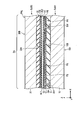
- FIG. 6 is a cross-sectional view showing a second configuration example of the display device DSP.
- the display device DSP shown in FIG. 6 has a different shape of the organic insulating film 21 as compared with the display device DSP shown in FIG.
- the film thickness of the organic insulating film 21 gradually increases from the incoming light side to the anti-light incident side.
- the organic insulating film 21 has a film thickness T11 in the first region AR1, a film thickness T12 in the second region AR2, a film thickness T13 in the third region AR3, and a film thickness T14 in the fourth region AR4. have.
- the film thickness T12 is larger than T11
- the film thickness T13 is larger than the film thickness T12
- the film thickness T14 is larger than the film thickness T13. That is, the surface 211 is formed in a stepped shape. Due to the shape of the organic insulating film 21, the distance D between the electrodes gradually decreases from the incoming light side to the anti-light incident side.
- the display device DSP has an inter-electrode distance D11 in the first region AR1, has an inter-electrode distance D12 in the second region AR2, has an inter-electrode distance D13 in the third region AR3, and has a fourth region.
- AR4 has a distance D14 between electrodes.
- the inter-electrode distance D12 is smaller than the inter-electrode distance D11
- the inter-electrode distance D13 is smaller than the inter-electrode distance D12
- the inter-electrode distance D14 is smaller than the inter-electrode distance D13.
- the film thickness of the organic insulating film 21 was 4 steps, but it may be 3 steps or less, or 5 steps or more. In such a second configuration example, the same effect as that of the first configuration example described above can be obtained.
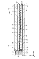
- FIG. 7 is a cross-sectional view showing a third configuration example of the display device DSP.
- the display device DSP shown in FIG. 7 has a different shape of the organic insulating film 21 as compared with the display device DSP shown in FIG.
- the surface 211 of the organic insulating film 21 is curved and recessed toward the transparent substrate 20.
- the same effect as that of the first configuration example described above can be obtained.
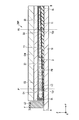
- FIG. 8 is a cross-sectional view showing a fourth configuration example of the display device DSP.
- the display device DSP shown in FIG. 8 adjusts the distance between the electrodes by the organic insulating film 11 of the first substrate SUB1 instead of the organic insulating film of the second substrate SUB2. It is different in that it is.
- the organic insulating film 11 has a film thickness T21 at the first position P1 and a film thickness T22 at the second position P2.
- the film thickness T21 is smaller than the film thickness T22.
- the film thickness of the organic insulating film 11 increases as the distance from the light emitting element LD increases.
- the surface 111 of the organic insulating film 11 on the second substrate SUB2 side is a slope with respect to the transparent substrate 10. Due to the shape of the organic insulating film 11 as described above, the distance D between the electrodes becomes smaller as the distance from the light emitting element LD increases. The second distance D2 is smaller than the first distance D1. As shown in FIGS. 3 and 8, at least one of the first substrate SUB1 and the second substrate SUB2 has an organic insulating film, and the film thickness at the first position P1 of the organic insulating film is the first of the organic insulating films. It is smaller than the film thickness at the two positions P2.
- FIG. 9 is a cross-sectional view schematically showing the display device DSP on the CD and EF lines shown in FIG.
- FIG. 9A is a cross-sectional view taken along the line CD.
- the position of the CD line is assumed to be the first position P1 shown in FIG.
- FIG. 9B is a cross-sectional view taken along the line EF.
- the position of the EF line is assumed to be the second position P2 shown in FIG.
- the organic insulating film 11 has a uniform film thickness T21 at the first position P1. Further, the first distance D1 is uniform at the first position P1.
- the first spacer SP1 has a height H11.
- the organic insulating film 11 has a uniform film thickness T22.
- the second distance D2 is uniform at the second position P2.
- the second spacer SP2 has a height H12.
- the height H11 of the first spacer SP1 is higher than the height H12 of the second spacer SP2. The height of the spacer decreases from the incoming light side to the anti-light incident side as well as the distance between the electrodes.
- the shape of the organic insulating film 11 of the fourth configuration example may be formed in a stepped shape as shown in FIG. 6, or may be a recessed shape as shown in FIG. 7.
- FIG. 10 is a cross-sectional view showing a fifth configuration example of the display device DSP.
- the display device DSP shown in FIG. 10 adjusts the distance between the electrodes by both the organic insulating film 21 of the second substrate SUB2 and the organic insulating film 11 of the first substrate SUB1 as compared with the display device DSP shown in FIG. It is different in that it is.
- the organic insulating film 11 has a film thickness T31 at the first position P1 and a film thickness T32 at the second position P2.
- the film thickness T31 is smaller than the film thickness T32.
- the film thickness of the organic insulating film 11 increases as the distance from the light emitting element LD increases.
- the surface 111 of the organic insulating film 11 on the second substrate SUB2 side is a slope with respect to the transparent substrate 10.
- the organic insulating film 21 has a film thickness T41 at the first position P1 and a film thickness T42 at the second position P2.
- the film thickness T41 is smaller than the film thickness T42.
- the film thickness of the organic insulating film 21 increases as the distance from the light emitting element LD increases. Therefore, the surface 211 of the organic insulating film 21 on the first substrate SUB1 side is a slope with respect to the transparent substrate 20. Due to the shapes of the organic insulating films 11 and 21, the distance D between the electrodes becomes smaller as the distance from the light emitting element LD increases.
- the second distance D2 is smaller than the first distance D1.
- FIG. 11 is a cross-sectional view schematically showing the display device DSP on the CD and EF lines shown in FIG.
- FIG. 11A is a cross-sectional view taken along the line CD.
- the position of the CD line is assumed to be the first position P1 shown in FIG.
- FIG. 11B is a cross-sectional view taken along the line EF.
- the position of the EF line is assumed to be the second position P2 shown in FIG.
- the organic insulating film 11 has a uniform film thickness T31, and the organic insulating film 21 has a uniform film thickness T41. Further, the first distance D1 is uniform at the first position P1.
- the first spacer SP1 has a height H21.
- the organic insulating film 11 has a uniform film thickness T32, and the organic insulating film 21 has a uniform film thickness T42. Further, the second distance D2 is uniform at the second position P2.
- the second spacer SP2 has a height H22. The height H21 of the first spacer SP1 is higher than the height H22 of the second spacer SP2.
- the height of the spacer decreases from the incoming light side to the anti-light incident side as well as the distance between the electrodes.
- the shapes of the organic insulating films 11 and 21 of the fifth configuration example may be formed in a stepped shape as shown in FIG. 6, or may be a recessed shape as shown in FIG. 7.
- FIG. 12 is a cross-sectional view showing a sixth configuration example of the display device DSP.
- the organic insulating film 11 of the first substrate SUB1 is arranged at a position where it overlaps with the scanning line G, the signal line S, and the switching element SW, and at a position where it overlaps with the pixel electrode PE. It differs in that it is not placed.
- FIG. 12 shows the configuration of the first substrate SUB1 of the pixel PX.
- the first substrate SUB1 includes a scanning line G, a signal line S intersecting the scanning line G, a switching element SW electrically connected to the scanning line G and the signal line S, a metal wiring M, and an organic insulating film 11.
- a capacitive electrode 13 and a pixel electrode PE or the like are provided.
- the two scanning lines G extend along the first direction X and are lined up in the second direction Y at intervals.
- Each of the two signal lines S extends along the second direction Y and is arranged at intervals in the first direction X.
- the pixel PX corresponds to a region partitioned by two signal lines S and two scanning lines G.
- the switching element SW is arranged at the intersection of the scanning line G and the signal line S.
- the organic insulating film 11 is patterned and formed in a grid pattern in a plan view. That is, the organic insulating film 11 is superimposed on the scanning line G, the signal line S, and the switching element SW, respectively.
- the organic insulating film 11 includes a first part 11X superimposing on the scanning line G and a second part 11Y superimposing on the signal line S.
- the first part 11X has a first side surface E1 close to the light emitting element LD and a second side surface E2 on the opposite side of the first side surface E1.
- the first side surface E1 and the second side surface E2 extend along the extension direction DR1 of the polymer 31.
- the second part 11Y has a third side surface E3 and a fourth side surface E4 on the opposite side of the third side surface E3.
- the region in which the organic insulating film 11 is arranged is referred to as the first region A1 of the first substrate SUB1, and the region in which the organic insulating film 11 is not arranged is referred to as the second region A2 of the first substrate SUB1. ..
- the second region A2 is located inside surrounded by the first region A1.
- the metal wiring M is arranged in the first region A1 and is formed in a grid pattern in a plan view. That is, the metal wiring M is superimposed on the scanning line G, the signal line S, and the switching element SW, respectively.
- the metal wiring M includes a first wiring portion MX superposed on the scanning line G and the first portion 11X, and a second wiring portion MY superimposing on the signal line S and the second portion 11Y.
- the capacitive electrode 13 is arranged over a plurality of pixels PX, and further is arranged over almost the entire area of the first substrate SUB1. That is, the capacitance electrodes 13 are arranged in the first region A1 and the second region A2, respectively.
- the capacitive electrode 13 is superimposed on the switching element SW, the scanning line G, the signal line S, and the organic insulating film 11 in the first region A1.
- the pixel electrode PE is superimposed on the capacitance electrode 13 in the second region A2.
- the pixel electrode PE is provided inside the region where the organic insulating film 11 is arranged.
- the pixel electrode PE may be provided so as to overlap each of the first part 11X and the second part 11Y.
- the spacer SP is superimposed on the switching element SW.
- FIG. 13 is a cross-sectional view schematically showing the display device DSP on the GH line shown in FIG.
- FIG. 13 illustrates the signal line S, the insulating films 8 and 9, and the metal wiring M on the first substrate SUB1, and illustrates the light-shielding layer BM on the second substrate SUB2.
- the insulating film 8 covers the transparent substrate 10.
- another conductive layer (light-shielding layer or reflective layer) formed of the same material as the scanning line G may be provided between the insulating film 8 and the transparent substrate 10.
- the signal line S is formed on the insulating film 8.
- the signal line S is located between the pixel electrodes PE adjacent to the first direction X.
- the insulating film 9 covers the signal line S and the insulating film 8.
- the organic insulating film 11 is located on the insulating film 9.
- the second portion 11Y of the organic insulating film 11 is located directly above the signal line S and is located between the pixel electrodes PE adjacent to the first direction X.
- the third side surface E3 and the fourth side surface E4 of the second part 11Y are covered with the capacitance electrode 13.
- Each of the third side surface E3 and the fourth side surface E4 is located between the signal line S and the pixel electrode PE along the first direction X.
- the organic insulating film 11 is not provided between the transparent substrate 10 and the pixel electrode PE.
- the total volume of the organic insulating film 11 is smaller than that in the case where the organic insulating film 11 is provided between the transparent substrate 10 and the pixel electrode PE (or the entire area of the display unit DA).
- the probability that the light propagating through the display panel PNL is incident on the organic insulating film 11 is reduced, so that the light absorption by the organic insulating film 11 can be suppressed. Therefore, deterioration of display quality can be suppressed.
- the second wiring portion MY of the metal wiring M is located on the organic insulating film 11.
- the second wiring portion MY is located directly above the signal line S. Further, the second wiring portion MY is in contact with the capacitance electrode 13 and is electrically connected to each other.
- the second part 11Y is located between the signal line S and the second wiring part MY.
- the light-shielding layer BM is located between the transparent substrate 20 and the organic insulating film 21.
- the light-shielding layer BM is located directly above the third side surface E3 and the fourth side surface E4 of the second part 11Y, and directly above the signal line S.
- the organic insulating film 21 may have the configurations shown in the first to third configuration examples. In such a sixth configuration example, the same effect as that of the first configuration example described above can be obtained.
- a light emitting element facing the end surface of the second substrate is provided.
- the common electrode is separated from the pixel electrode by a first distance.
- the common electrode is separated from the pixel electrode by a second distance.
- the second substrate has a first transparent substrate and a first organic insulating film located between the first transparent substrate and the common electrode.
- the display device wherein the film thickness of the first organic insulating film at the first position is smaller than the film thickness of the first organic insulating film at the second position. (3) The display device according to (2), wherein the film thickness of the first organic insulating film gradually increases from the first position to the second position. (4) The display device according to (2), wherein the surface of the first organic insulating film on the first substrate side is stepped. (5) The display device according to (2), wherein the surface of the first organic insulating film on the first substrate side is curved. (6) Further, a first spacer at the first position and a second spacer at the second position are provided. The display device according to (1), wherein the height of the first spacer is higher than the height of the second spacer.
- the first substrate has a second transparent substrate and a second organic insulating film located between the second transparent substrate and the pixel electrode.
- the second substrate has a first transparent substrate and a first organic insulating film located between the first transparent substrate and the common electrode.
- the display device according to (7), wherein the film thickness of the first organic insulating film at the first position is smaller than the film thickness of the first organic insulating film at the second position.
- the first substrate has a second transparent substrate and has a second transparent substrate.
- an insulating film With an insulating film, The display device according to (1), wherein the second organic insulating film is not provided between the second transparent substrate and the pixel electrode.
- the second organic insulating film is superimposed on the scanning line and the signal line.
- a liquid crystal layer located between the first substrate and the second substrate, A light emitting element facing the first end surface is provided.
- the second substrate has a first position and a second position located between the first position and the second end face.
- a display device in which the distance between the first electrode and the second electrode at the first position is larger than the distance between the first electrode and the second electrode at the second position.
- At least one of the first substrate and the second substrate has an organic insulating film.
- liquid crystal layer is sealed between the first substrate and the second substrate by a seal.
- a light emitting element facing a seal located on the side of the first end face in the direction from the first end face to the second end face is provided.
- the second substrate has a first position and a second position located between the first position and the second end face. At least one of the first substrate and the second substrate has an organic insulating film.
- the first substrate has a plurality of first electrodes and has a plurality of first electrodes.
- the second substrate has at least one second electrode.
- the liquid crystal layer contains a polymer-dispersed liquid crystal and contains.
Landscapes
- Physics & Mathematics (AREA)
- Nonlinear Science (AREA)
- Chemical & Material Sciences (AREA)
- General Physics & Mathematics (AREA)
- Mathematical Physics (AREA)
- Crystallography & Structural Chemistry (AREA)
- Optics & Photonics (AREA)
- Dispersion Chemistry (AREA)
- Engineering & Computer Science (AREA)
- Geometry (AREA)
- Theoretical Computer Science (AREA)
- General Engineering & Computer Science (AREA)
- Devices For Indicating Variable Information By Combining Individual Elements (AREA)
- Liquid Crystal (AREA)
- Electroluminescent Light Sources (AREA)
- Planar Illumination Modules (AREA)
Abstract
画素電極を有する第1基板と、共通電極を有する第2基板と、前記第1基板と前記第2基板との間に位置し、ポリマーと、液晶分子とを含む液晶層と、前記第2基板の端面に対向する発光素子と、を備え、第1位置において前記共通電極は前記画素電極から第1距離だけ離間しており、前記第1位置より前記発光素子から離間した第2位置において前記共通電極は前記画素電極から第2距離だけ離間しており、前記第2距離は、前記第1距離より小さい、表示装置。
Description
本発明の実施形態は、表示装置に関する。
高分子分散液晶(PDLC;Polymer Dispersed Liquid Crystal)を用いて透明と散乱を切り替える表示装置が提案されている。これは、映り込み防止などを目的としたものであり、PDLCに対して部分的に電圧を印加して透明と散乱を切り替える技術である。PDLCを使用した透明な表示装置には、導光板の端部に光源を配置するエッジライト方式が採用されている。しかし、エッジライト方式をPDLC表示装置に用いると、光源から離れるにつれて輝度が低下するという問題があった。
本実施形態の目的は、表示品位の低下を抑制することが可能な表示装置を提供することにある。
本実施形態によれば、画素電極を有する第1基板と、共通電極を有する第2基板と、前記第1基板と前記第2基板との間に位置し、ポリマーと、液晶分子とを含む液晶層と、前記第2基板の端面に対向する発光素子と、を備え、第1位置において前記共通電極は前記画素電極から第1距離だけ離間しており、前記第1位置より前記発光素子から離間した第2位置において前記共通電極は前記画素電極から第2距離だけ離間しており、前記第2距離は、前記第1距離より小さい、表示装置が提供される。
以下、本実施形態について、図面を参照しながら説明する。なお、開示はあくまで一例に過ぎず、当業者において、発明の主旨を保っての適宜変更について容易に想到し得るものについては、当然に本発明の範囲に含有されるものである。また、図面は、説明をより明確にするため、実際の態様に比べて、各部の幅、厚さ、形状等について模式的に表される場合があるが、あくまで一例であって、本発明の解釈を限定するものではない。また、本明細書と各図において、既出の図に関して前述したものと同一又は類似した機能を発揮する構成要素には同一の参照符号を付し、重複する詳細な説明を適宜省略することがある。
[第1構成例]
図1は、本実施形態の表示装置DSPの一例を示す平面図である。
一例では、第1方向X、第2方向Y、及び、第3方向Zは、互いに直交しているが、90度以外の角度で交差していてもよい。第1方向X及び第2方向Yは、表示装置DSPを構成する基板の主面と平行な方向に相当し、第3方向Zは、表示装置DSPの厚さ方向に相当する。本明細書において、第1基板SUB1から第2基板SUB2に向かう方向を「上側」(あるいは、単に上)と称し、第2基板SUB2から第1基板SUB1に向かう方向を「下側」(あるいは、単に下)と称する。「第1部材の上の第2部材」及び「第1部材の下の第2部材」とした場合、第2部材は、第1部材に接していてもよいし、第1部材から離間していてもよい。また、第3方向Zを示す矢印の先端側に表示装置DSPを観察する観察位置があるものとし、この観察位置から、第1方向X及び第2方向Yで規定されるX-Y平面に向かって見ることを平面視という。
図1は、本実施形態の表示装置DSPの一例を示す平面図である。
一例では、第1方向X、第2方向Y、及び、第3方向Zは、互いに直交しているが、90度以外の角度で交差していてもよい。第1方向X及び第2方向Yは、表示装置DSPを構成する基板の主面と平行な方向に相当し、第3方向Zは、表示装置DSPの厚さ方向に相当する。本明細書において、第1基板SUB1から第2基板SUB2に向かう方向を「上側」(あるいは、単に上)と称し、第2基板SUB2から第1基板SUB1に向かう方向を「下側」(あるいは、単に下)と称する。「第1部材の上の第2部材」及び「第1部材の下の第2部材」とした場合、第2部材は、第1部材に接していてもよいし、第1部材から離間していてもよい。また、第3方向Zを示す矢印の先端側に表示装置DSPを観察する観察位置があるものとし、この観察位置から、第1方向X及び第2方向Yで規定されるX-Y平面に向かって見ることを平面視という。
本実施形態においては、表示装置DSPの一例として、高分子分散型液晶を適用した液晶表示装置について説明する。表示装置DSPは、表示パネルPNLと、配線基板1と、ICチップ2と、発光素子LDと、を備えている。
表示パネルPNLは、第1基板SUB1と、第2基板SUB2と、液晶層LCと、シールSLと、を備えている。第1基板SUB1及び第2基板SUB2は、X-Y平面と平行な平板状に形成されている。第1基板SUB1及び第2基板SUB2は、平面視で、重畳している。第1基板SUB1及び第2基板SUB2は、シールSLによって接着されている。液晶層LCは、第1基板SUB1と第2基板SUB2との間に保持され、シールSLによって封止されている。図1において、液晶層LC及びシールSLは、異なる斜線で示している。
図1において拡大して模式的に示すように、液晶層LCは、ポリマー31と、液晶分子32と、を含む高分子分散型液晶を備えている。一例では、ポリマー31は、液晶性ポリマーである。ポリマー31は、一方向に沿って延出した筋状に形成されている。例えば、ポリマー31の延出方向DR1は、第1方向Xに沿った方向である。液晶分子32は、ポリマー31の隙間に分散され、その長軸が第1方向Xに沿うように配向される。ポリマー31及び液晶分子32の各々は、光学異方性あるいは屈折率異方性を有している。ポリマー31の電界に対する応答性は、液晶分子32の電界に対する応答性より低い。
一例では、ポリマー31の配向方向は、電界の有無にかかわらずほとんど変化しない。一方、液晶分子32の配向方向は、液晶層LCにしきい値以上の高い電圧が印加された状態では、電界に応じて変化する。液晶層LCに電圧が印加されていない状態では、ポリマー31及び液晶分子32のそれぞれの光軸は互いに平行であり、液晶層LCに入射した光は、液晶層LC内でほとんど散乱されることなく透過する(透明状態)。液晶層LCに電圧が印加された状態では、ポリマー31及び液晶分子32のそれぞれの光軸は互いに交差し、液晶層LCに入射した光は、液晶層LC内で散乱される(散乱状態)。
表示パネルPNLは、画像を表示する表示部DAと、表示部DAを囲む額縁状の非表示部NDAと、を備えている。シールSLは、非表示部NDAに位置している。表示部DAは、第1方向X及び第2方向Yにマトリクス状に配列された画素PXを備えている。
図1において拡大して示すように、各画素PXは、スイッチング素子SW、画素電極(第1電極)PE、共通電極(共通電極)CE、液晶層LC等を備えている。スイッチング素子SWは、例えば薄膜トランジスタ(TFT)によって構成され、走査線G及び信号線Sと電気的に接続されている。走査線Gは、第1方向Xに並んだ画素PXの各々におけるスイッチング素子SWと電気的に接続されている。信号線Sは、第2方向Yに並んだ画素PXの各々におけるスイッチング素子SWと電気的に接続されている。画素電極PEは、スイッチング素子SWと電気的に接続されている。画素電極PEの各々は、第3方向Zにおいて共通電極CEと対向し、画素電極PEと共通電極CEとの間に生じる電界によって液晶層LC(特に、液晶分子32)を駆動している。容量CSは、例えば、共通電極CEと同電位の電極、及び、画素電極PEと同電位の電極の間に形成される。なお、第1基板SUB1は、複数の画素電極PEを有している。第2基板SUB2は、少なくとも1つの共通電極CEを有している。
配線基板1は、第1基板SUB1の延出部Exに電気的に接続されている。配線基板1は、折り曲げ可能なフレキシブルプリント回路基板である。ICチップ2は、配線基板1に電気的に接続されている。ICチップ2は、例えば、画像表示に必要な信号を出力するディスプレイドライバなどを内蔵している。なお、ICチップ2は、延出部Exに電気的に接続されていてもよい。配線基板1及びICチップ2は、表示パネルPNLからの信号を読み出す場合もあるが、主として表示パネルPNLに信号を供給する信号源として機能する。
発光素子LDは、延出部Exに重畳している。複数の発光素子LDは、第1方向Xに沿って間隔をおいて並んでいる。これらの発光素子LDは、第2基板SUB2の端面(第1端面)E21に対向し、端面E21に向けて光を出射する。なお、第2基板SUB2は、端面E21の反対側に端面(第2端面)E22を有しており、発光素子LDから発光された光は、端面E22まで到達する。
図2は、図1に示した表示パネルPNLの表示部DAを示す断面図である。液晶層LCは、第1基板SUB1と第2基板SUB2との間に設けられている。
第1基板SUB1は、透明基板(第2透明基板)10と、有機絶縁膜(第2有機絶縁膜)11と、容量絶縁膜12と、容量電極13と、スイッチング素子SWと、画素電極PEと、配向膜AL1と、を備えている。
第1基板SUB1は、透明基板(第2透明基板)10と、有機絶縁膜(第2有機絶縁膜)11と、容量絶縁膜12と、容量電極13と、スイッチング素子SWと、画素電極PEと、配向膜AL1と、を備えている。
透明基板10は、主面10Aと、主面10Aの反対側の主面10Bと、を備えている。スイッチング素子SWは、主面10B側に配置されている。スイッチング素子SWは、半導体層の下にゲート電極が位置するボトムゲート型であってもよいし、半導体層の上にゲート電極が位置するトップゲート型であってもよい。半導体層は、例えばアモルファスシリコンによって形成されるが、多結晶シリコンや酸化物半導体によって形成されてもよい。
有機絶縁膜11は、スイッチング素子SWを覆っている。また、有機絶縁膜11は、透明基板10と画素電極PEとの間に位置している。なお、図1に示した走査線G及び信号線Sは、透明基板10と有機絶縁膜11との間に配置されているが、ここでは図示を省略している。走査線Gと、走査線Gと交差する信号線Sと、走査線G及び信号線Sと電気的に接続されたスイッチング素子SWと、スイッチング素子SWに重畳する有機絶縁膜11は、透明基板10上に位置している。容量電極13は、有機絶縁膜11及び容量絶縁膜12の間に配置されている。画素電極PEは、容量絶縁膜12と配向膜AL1との間において、画素PX毎に配置されている。画素電極PEは、容量電極13の開口部OPを介してスイッチング素子SWと電気的に接続されている。画素電極PEは、容量絶縁膜12を挟んで、容量電極13と重畳し、画素PXの容量CSを形成している。配向膜AL1は、画素電極PEを覆っている。配向膜AL1は、液晶層LCに接している。
第2基板SUB2は、透明基板(第1透明基板)20と、共通電極CEと、有機絶縁膜(第1有機絶縁膜)21と、配向膜AL2と、を備えている。透明基板20は、主面20Aと、主面20Aの反対側の主面20Bと、を備えている。透明基板20の主面20Aは、透明基板10の主面10Bと向かい合っている。有機絶縁膜21は、主面20Aに設けられており、透明基板20と共通電極CEとの間に位置している。共通電極CEは、液晶層LCと有機絶縁膜21との間に設けられている。共通電極CEは、複数の画素PXに亘って配置され、第3方向Zにおいて、複数の画素電極PEと対向している。配向膜AL2は、共通電極CEを覆っている。また、配向膜AL2は、液晶層LCに接している。なお、第2基板SUB2は、走査線G、信号線S、及び、スイッチング素子SWの直上に遮光層を備えていてもよい。
透明基板10及び20は、ガラス基板やプラスチック基板などの絶縁基板である。有機絶縁膜11及び21は、アクリル樹脂などの透明な絶縁材料によって形成されている。容量絶縁膜12は、シリコン窒化物などの無機絶縁膜である。容量電極13、画素電極PE、共通電極CEは、インジウム錫酸化物(ITO)やインジウム亜鉛酸化物(IZO)などの透明導電材料によって形成された透明電極である。配向膜AL1及びAL2は、例えば第1方向Xに沿って配向処理されている。なお、配向処理とは、ラビング処理であってもよいし、光配向処理であってもよい。
図3は、図1に示したA-B線における表示装置DSPを概略的に示す断面図である。ここでは、本発明の主要な構成のみを示し、他の部材の図示を省略している。
カバー部材CMは、透明基板20の上に位置している。発光素子LDは、カバー部材CM、透明基板20、液晶層LC、シールSLと第2方向Yに対向している。発光素子LDは、端面E21から端面E22への方向で、端面E21側に位置するシールSLと対向している。また、発光素子LDは、配線基板Fに電気的に接続されている。なお、発光素子LDと透明基板20との間に導光体が介在していても良い。画素電極PEと共通電極CEとの間に印加される電圧によって発光素子LDから液晶層LCへ入射した光の散乱状態を変化させる。
カバー部材CMは、透明基板20の上に位置している。発光素子LDは、カバー部材CM、透明基板20、液晶層LC、シールSLと第2方向Yに対向している。発光素子LDは、端面E21から端面E22への方向で、端面E21側に位置するシールSLと対向している。また、発光素子LDは、配線基板Fに電気的に接続されている。なお、発光素子LDと透明基板20との間に導光体が介在していても良い。画素電極PEと共通電極CEとの間に印加される電圧によって発光素子LDから液晶層LCへ入射した光の散乱状態を変化させる。
ここで、発光素子LDに近い第1位置P1と、第1位置P1より発光素子LDから離間した第2位置P2と、を定義する。第2基板SUB2は、第1位置P1と、第2位置P2と、を有している。第2位置P2は、第1位置P1と端面E22との間に位置している。有機絶縁膜21は、第1位置P1において膜厚T1を有し、第2位置P2において膜厚T2を有している。膜厚T1は、膜厚T2より小さい。有機絶縁膜21の膜厚は、発光素子LDから離れるに連れて大きくなっている。つまり、有機絶縁膜21の膜厚は、第1位置P1から第2位置P2へ漸次大きくなる。そのため、有機絶縁膜21の第1基板SUB1側の面211は、透明基板20に対して斜面である。このような、有機絶縁膜21の形状によって、共通電極CEと画素電極PEとの間の電極間距離Dは、発光素子LDから離れるに連れて小さくなる。第1位置P1において共通電極CEは画素電極PEから第1距離D1だけ離間している。第2位置P2において共通電極CEは画素電極PEから第2距離D2だけ離間している。第2距離D2は、第1距離D1より小さい。換言すると、第1位置P1における画素電極PEと共通電極CEとの間の第1距離D1は、第2位置P2における画素電極PEと共通電極CEとの間の第2距離D2よりも大きい。つまり、画素電極PEと共通電極CEとの間の距離は、第1位置P1から第2位置P2へ漸次小さくなる。また、端面E21側に位置するシールSLの厚さSLT1は、端面E22側に位置するシールSLの厚さSLT2よりも大きい。液晶層LCの厚さLCTは、端面E21から端面E22へ漸次小さくなる。
高分子分散型液晶を適用した表示装置DSPにおいては、発光素子LDは、第2基板SUB2の端面E21と対向して位置している。そのため、発光素子LDから発光された光は、配線、遮光層、有機絶縁膜などによって吸収されたり、散乱に用いられたりすることによって、発光素子LDから遠ざかるに連れて減少していく。すなわち、入光側から反入光側にかけて表示装置DSPの輝度が低下する恐れがある。ここで、入光側とは、発光素子LDが位置する側である端面E21側に相当し、反入光側とは、端面E21の反対側の端面E22側に相当する。
本実施形態によれば、共通電極CEと画素電極PEとの間の電極間距離Dが、発光素子LDから遠ざかるに連れて小さくなるため、共通電極CEと画素電極PEとの間の電界強度が発光素子LDから遠ざかるに連れて強くなる。そのため、入光側から反入光側にかけての輝度の低下を抑制することができる。よって、表示装置DSPの表示品位の低下を抑制することができる。
図4は、図1に示したC-D線、E-F線における表示装置DSPを概略的に示す断面図である。図4(a)は、C-D線における断面図である。C-D線の位置は、図3に示した第1位置P1であるとする。図4(b)は、E-F線における断面図である。E-F線の位置は、図3に示した第2位置P2であるとする。
図4(a)に示すように、第1位置P1においては、有機絶縁膜21は均一の膜厚T1を有している。また、第1距離D1は、第1位置P1において均一である。表示装置DSPは、第1位置P1に第1スペーサSP1を有している。第1スペーサSP1は、高さH1を有している。このようなスペーサは、第1基板SUB1と第2基板SUB2との間に所定のセルギャップを形成し、例えば、画素PXごとに配置されている。図4(b)に示すように、第2位置P2においては、有機絶縁膜21は均一の膜厚T2を有している。また、第2距離D2は、第2位置P2において均一である。本実施形態では、入光側から反入光側に向かう方向に対して垂直な方向においては、有機絶縁膜21の膜厚及び電極間距離Dは均一である。換言すると、図1に示した表示装置DSPのY-Z断面では、有機絶縁膜21の膜厚及び電極間距離Dは位置によって変化するが、X-Z断面では、有機絶縁膜21の膜厚及び電極間距離Dは一定である。表示装置DSPは、第2位置P2に第2スペーサSP2を有している。第2スペーサSP2は、高さH2を有している。第1スペーサSP1の高さH1は、第2スペーサSP2の高さH2よりも高い。つまり、スペーサの高さは、電極間距離と同様に、入光側から反入光側にかけて小さくなっている。
なお、本実施形態では有機絶縁膜21の形状によって電極間距離を調整しているが、スペーサの高さによって調整しても良い。この場合、有機絶縁膜21の膜厚は入光側から反入光側にかけて均一であっても良いし、形成されていなくても良い。また、後述するが、電極間距離を調整するための有機絶縁膜は、第2基板SUB2ではなく、第1基板SUB1に形成されていても良い。または、第1基板SUB1と第2基板SUB2の両方に形成されていても良い。入光側から反入光側へ電極間距離を小さくしていく度合いは用途に応じて任意に変えることができる。
図5は、電極間距離、電界強度、規格化輝度の関係を示す図である。
図5(a)は、入光側から反入光側にかけて電極間距離Dが均一である場合を示している。すなわち、第1距離D1と第2距離D2とは等しい。例えば、均一な電極間距離Dは、約3μmである。このとき、第1位置P1での輝度L1及び第2位置P2での輝度L2の比は、5:2である。第1位置P1の輝度L1に対して第2位置P2の輝度L2は、60%減少している。輝度が均一に視認されるためには、輝度が低下しないと仮定した場合の輝度L1及びL2が2:5になるように第1距離D1及び第2距離D2を設定すれば良い。
図5(a)は、入光側から反入光側にかけて電極間距離Dが均一である場合を示している。すなわち、第1距離D1と第2距離D2とは等しい。例えば、均一な電極間距離Dは、約3μmである。このとき、第1位置P1での輝度L1及び第2位置P2での輝度L2の比は、5:2である。第1位置P1の輝度L1に対して第2位置P2の輝度L2は、60%減少している。輝度が均一に視認されるためには、輝度が低下しないと仮定した場合の輝度L1及びL2が2:5になるように第1距離D1及び第2距離D2を設定すれば良い。
図5(b)は、電界強度と規格化輝度の関係を示すグラフである。
グラフの横軸は、電界強度[MV/m]を示し、グラフの縦軸は、規格化輝度を示している。図5(a)に示した電極間距離Dが3μmである場合の電界強度を電界強度V0とする。電極間距離Dが3μmより小さい場合には、電界強度は電界強度V0より大きくなり規格化輝度も増加する。また、電極間距離Dが3μmより大きい場合には、電界強度は電界強度V0より小さくなり規格化輝度も減少する。ここでは、電界強度V0より小さい電界強度V1が第1位置P1にかかり、電界強度V0より大きい電界強度V2が第2位置P2にかかるようにする。入光側から反入光側にかけての輝度の低下が生じないと仮定すると、電界強度がV1のとき、規格化輝度L11が第1位置P1で得られ、電界強度がV2のとき、規格化輝度L12が第2位置P2で得られる。規格化輝度L11及びL12の比は、2:5に近い数値となる。
グラフの横軸は、電界強度[MV/m]を示し、グラフの縦軸は、規格化輝度を示している。図5(a)に示した電極間距離Dが3μmである場合の電界強度を電界強度V0とする。電極間距離Dが3μmより小さい場合には、電界強度は電界強度V0より大きくなり規格化輝度も増加する。また、電極間距離Dが3μmより大きい場合には、電界強度は電界強度V0より小さくなり規格化輝度も減少する。ここでは、電界強度V0より小さい電界強度V1が第1位置P1にかかり、電界強度V0より大きい電界強度V2が第2位置P2にかかるようにする。入光側から反入光側にかけての輝度の低下が生じないと仮定すると、電界強度がV1のとき、規格化輝度L11が第1位置P1で得られ、電界強度がV2のとき、規格化輝度L12が第2位置P2で得られる。規格化輝度L11及びL12の比は、2:5に近い数値となる。
図5(c)は、入光側から反入光側にかけて電極間距離Dが小さくなる場合を示している。第1位置P1において、電極間距離Dは、電界強度V1が得られる第1距離D1に設定されている。また、第2位置P2において、電極間距離Dは、電界強度V2が得られる第2距離D2に設定されている。このとき、例えば、第1距離D1は3μmより大きく、第2距離D2は3μmより小さい。例えば、第1距離D1は約4.4μmであり、第2距離D2は約2.5μmである。このように電極間距離を調整することによって、均一な電圧を与えた場合にも、電界強度は入光側から反入光側にかけて増加し、視認される輝度を均一にすることができる。
[第2構成例]
図6は、表示装置DSPの第2構成例を示す断面図である。図6に示す表示装置DSPは、図3に示した表示装置DSPと比較して、有機絶縁膜21の形状が異なっている。
図6は、表示装置DSPの第2構成例を示す断面図である。図6に示す表示装置DSPは、図3に示した表示装置DSPと比較して、有機絶縁膜21の形状が異なっている。
有機絶縁膜21は、入光側から反入光側にかけて段階的に膜厚が大きくなっている。有機絶縁膜21は、第1領域AR1において膜厚T11を有し、第2領域AR2において膜厚T12を有し、第3領域AR3において膜厚T13を有し、第4領域AR4において膜厚T14を有している。膜厚T12はT11より大きく、膜厚T13は膜厚T12より大きく、膜厚T14は膜厚T13より大きい。すなわち、面211は、階段状に形成されている。このような有機絶縁膜21の形状により、電極間距離Dは、入光側から反入光側にかけて段階的に小さくなっている。表示装置DSPは、第1領域AR1においては電極間距離D11を有し、第2領域AR2においては電極間距離D12を有し、第3領域AR3においては電極間距離D13を有し、第4領域AR4においては電極間距離D14を有する。電極間距離D12は電極間距離D11より小さく、電極間距離D13は電極間距離D12より小さく、電極間距離D14は電極間距離D13より小さい。なお、図示した例では、有機絶縁膜21の膜厚は4段階であったが、3段階以内でも良いし、5段階以上でもよい。
このような第2構成例においても、上記した第1構成例と同様の効果を得ることができる。
このような第2構成例においても、上記した第1構成例と同様の効果を得ることができる。
[第3構成例]
図7は、表示装置DSPの第3構成例を示す断面図である。図7に示す表示装置DSPは、図3に示した表示装置DSPと比較して、有機絶縁膜21の形状が異なっている。
有機絶縁膜21の面211は、湾曲し、透明基板20側に凹んでいる。
このような第3構成例においても、上記した第1構成例と同様の効果を得ることができる。
図7は、表示装置DSPの第3構成例を示す断面図である。図7に示す表示装置DSPは、図3に示した表示装置DSPと比較して、有機絶縁膜21の形状が異なっている。
有機絶縁膜21の面211は、湾曲し、透明基板20側に凹んでいる。
このような第3構成例においても、上記した第1構成例と同様の効果を得ることができる。
[第4構成例]
図8は、表示装置DSPの第4構成例を示す断面図である。図8に示す表示装置DSPは、図3に示した表示装置DSPと比較して、第2基板SUB2の有機絶縁膜ではなく、第1基板SUB1の有機絶縁膜11によって電極間距離を調整している点で異なっている。
有機絶縁膜11は、第1位置P1において膜厚T21を有し、第2位置P2において膜厚T22を有している。膜厚T21は、膜厚T22より小さい。有機絶縁膜11の膜厚は、発光素子LDから離れるに連れて大きくなっている。そのため、有機絶縁膜11の第2基板SUB2側の面111は、透明基板10に対して斜面である。このような、有機絶縁膜11の形状によって、電極間距離Dは、発光素子LDから離れるに連れて小さくなる。第2距離D2は、第1距離D1より小さい。
図3及び図8に示したように、第1基板SUB1と第2基板SUB2の少なくとも一方は、有機絶縁膜を有し、有機絶縁膜の第1位置P1における膜厚は、有機絶縁膜の第2位置P2における膜厚より小さい。
図8は、表示装置DSPの第4構成例を示す断面図である。図8に示す表示装置DSPは、図3に示した表示装置DSPと比較して、第2基板SUB2の有機絶縁膜ではなく、第1基板SUB1の有機絶縁膜11によって電極間距離を調整している点で異なっている。
有機絶縁膜11は、第1位置P1において膜厚T21を有し、第2位置P2において膜厚T22を有している。膜厚T21は、膜厚T22より小さい。有機絶縁膜11の膜厚は、発光素子LDから離れるに連れて大きくなっている。そのため、有機絶縁膜11の第2基板SUB2側の面111は、透明基板10に対して斜面である。このような、有機絶縁膜11の形状によって、電極間距離Dは、発光素子LDから離れるに連れて小さくなる。第2距離D2は、第1距離D1より小さい。
図3及び図8に示したように、第1基板SUB1と第2基板SUB2の少なくとも一方は、有機絶縁膜を有し、有機絶縁膜の第1位置P1における膜厚は、有機絶縁膜の第2位置P2における膜厚より小さい。
図9は、図1に示したC-D線、E-F線における表示装置DSPを概略的に示す断面図である。図9(a)は、C-D線における断面図である。C-D線の位置は、図8に示した第1位置P1であるとする。図9(b)は、E-F線における断面図である。E-F線の位置は、図8に示した第2位置P2であるとする。
図9(a)に示すように、第1位置P1においては、有機絶縁膜11は均一の膜厚T21を有している。また、第1距離D1は、第1位置P1において均一である。第1スペーサSP1は、高さH11を有している。図9(b)に示すように、第2位置P2においては、有機絶縁膜11は均一の膜厚T22を有している。また、第2距離D2は、第2位置P2において均一である。第2スペーサSP2は、高さH12を有している。第1スペーサSP1の高さH11は、第2スペーサSP2の高さH12よりも高い。スペーサの高さは、電極間距離と同様に、入光側から反入光側にかけて小さくなっている。
このような第4構成例においても、上記した第1構成例と同様の効果を得ることができる。なお、第4構成例の有機絶縁膜11の形状を図6に示したような階段状に形成しても良いし、図7に示したような窪んだ形状としても良い。
このような第4構成例においても、上記した第1構成例と同様の効果を得ることができる。なお、第4構成例の有機絶縁膜11の形状を図6に示したような階段状に形成しても良いし、図7に示したような窪んだ形状としても良い。
[第5構成例]
図10は、表示装置DSPの第5構成例を示す断面図である。図10に示す表示装置DSPは、図3に示した表示装置DSPと比較して、第2基板SUB2の有機絶縁膜21及び第1基板SUB1の有機絶縁膜11の両方によって電極間距離を調整している点で異なっている。
有機絶縁膜11は、第1位置P1において膜厚T31を有し、第2位置P2において膜厚T32を有している。膜厚T31は、膜厚T32より小さい。有機絶縁膜11の膜厚は、発光素子LDから離れるに連れて大きくなっている。そのため、有機絶縁膜11の第2基板SUB2側の面111は、透明基板10に対して斜面である。有機絶縁膜21は、第1位置P1において膜厚T41を有し、第2位置P2において膜厚T42を有している。膜厚T41は、膜厚T42より小さい。有機絶縁膜21の膜厚は、発光素子LDから離れるに連れて大きくなっている。そのため、有機絶縁膜21の第1基板SUB1側の面211は、透明基板20に対して斜面である。このような、有機絶縁膜11及び21の形状によって、電極間距離Dは、発光素子LDから離れるに連れて小さくなる。第2距離D2は、第1距離D1より小さい。
図10は、表示装置DSPの第5構成例を示す断面図である。図10に示す表示装置DSPは、図3に示した表示装置DSPと比較して、第2基板SUB2の有機絶縁膜21及び第1基板SUB1の有機絶縁膜11の両方によって電極間距離を調整している点で異なっている。
有機絶縁膜11は、第1位置P1において膜厚T31を有し、第2位置P2において膜厚T32を有している。膜厚T31は、膜厚T32より小さい。有機絶縁膜11の膜厚は、発光素子LDから離れるに連れて大きくなっている。そのため、有機絶縁膜11の第2基板SUB2側の面111は、透明基板10に対して斜面である。有機絶縁膜21は、第1位置P1において膜厚T41を有し、第2位置P2において膜厚T42を有している。膜厚T41は、膜厚T42より小さい。有機絶縁膜21の膜厚は、発光素子LDから離れるに連れて大きくなっている。そのため、有機絶縁膜21の第1基板SUB1側の面211は、透明基板20に対して斜面である。このような、有機絶縁膜11及び21の形状によって、電極間距離Dは、発光素子LDから離れるに連れて小さくなる。第2距離D2は、第1距離D1より小さい。
図11は、図1に示したC-D線、E-F線における表示装置DSPを概略的に示す断面図である。図11(a)は、C-D線における断面図である。C-D線の位置は、図10に示した第1位置P1であるとする。図11(b)は、E-F線における断面図である。E-F線の位置は、図10に示した第2位置P2であるとする。
図11(a)に示すように、第1位置P1においては、有機絶縁膜11は均一の膜厚T31を有し、有機絶縁膜21は均一の膜厚T41を有している。また、第1距離D1は、第1位置P1において均一である。第1スペーサSP1は、高さH21を有している。図11(b)に示すように、第2位置P2においては、有機絶縁膜11は均一の膜厚T32を有し、有機絶縁膜21は均一の膜厚T42を有している。また、第2距離D2は、第2位置P2において均一である。第2スペーサSP2は、高さH22を有している。第1スペーサSP1の高さH21は、第2スペーサSP2の高さH22よりも高い。スペーサの高さは、電極間距離と同様に、入光側から反入光側にかけて小さくなっている。
このような第5構成例においても、上記した第1構成例と同様の効果を得ることができる。なお、第5構成例の有機絶縁膜11及び21の形状を図6に示したような階段状に形成しても良いし、図7に示したような窪んだ形状としても良い。
このような第5構成例においても、上記した第1構成例と同様の効果を得ることができる。なお、第5構成例の有機絶縁膜11及び21の形状を図6に示したような階段状に形成しても良いし、図7に示したような窪んだ形状としても良い。
[第6構成例]
図12は、表示装置DSPの第6構成例を示す断面図である。第6構成例は、第1構成例と比較して、第1基板SUB1の有機絶縁膜11が走査線G、信号線S、スイッチング素子SWと重なる位置に配置され、画素電極PEと重なる位置に配置されていない点で異なっている。
図12は、画素PXの第1基板SUB1の構成を示している。第1基板SUB1は、走査線Gと、走査線Gと交差する信号線Sと、走査線G及び信号線Sと電気的に接続されたスイッチング素子SWと、金属配線Mと、有機絶縁膜11と、容量電極13と、画素電極PE等を備えている。
図12は、表示装置DSPの第6構成例を示す断面図である。第6構成例は、第1構成例と比較して、第1基板SUB1の有機絶縁膜11が走査線G、信号線S、スイッチング素子SWと重なる位置に配置され、画素電極PEと重なる位置に配置されていない点で異なっている。
図12は、画素PXの第1基板SUB1の構成を示している。第1基板SUB1は、走査線Gと、走査線Gと交差する信号線Sと、走査線G及び信号線Sと電気的に接続されたスイッチング素子SWと、金属配線Mと、有機絶縁膜11と、容量電極13と、画素電極PE等を備えている。
2本の走査線Gは、それぞれ第1方向Xに沿って延出し、第2方向Yに間隔をおいて並んでいる。2本の信号線Sは、それぞれ第2方向Yに沿って延出し、第1方向Xに間隔をおいて並んでいる。画素PXは、2本の信号線Sと、2本の走査線Gとで区画された領域に相当する。スイッチング素子SWは、走査線Gと信号線Sとの交差部に配置されている。
有機絶縁膜11は、パターン化されており、平面視で格子状に形成されている。すなわち、有機絶縁膜11は、走査線G、信号線S、及び、スイッチング素子SWのそれぞれに重畳している。有機絶縁膜11は、走査線Gに重畳する第1部11Xと、信号線Sに重畳する第2部11Yと、を備えている。第1部11Xは、発光素子LDに近接した第1側面E1と、第1側面E1の反対側の第2側面E2と、を有している。第1側面E1及び第2側面E2は、ポリマー31の延出方向DR1に沿って延出している。第2部11Yは、第3側面E3と、第3側面E3の反対側の第4側面E4と、を有している。
なお、図12において、有機絶縁膜11が配置された領域を第1基板SUB1の第1領域A1と称し、有機絶縁膜11が配置されていない領域を第1基板SUB1の第2領域A2と称する。第2領域A2は、第1領域A1によって囲まれた内側に位置している。
なお、図12において、有機絶縁膜11が配置された領域を第1基板SUB1の第1領域A1と称し、有機絶縁膜11が配置されていない領域を第1基板SUB1の第2領域A2と称する。第2領域A2は、第1領域A1によって囲まれた内側に位置している。
金属配線Mは、第1領域A1に配置され、平面視で格子状に形成されている。すなわち、金属配線Mは、走査線G、信号線S、及び、スイッチング素子SWのそれぞれに重畳している。金属配線Mは、走査線G及び第1部11Xに重畳する第1配線部MXと、信号線S及び第2部11Yに重畳する第2配線部MYと、を備えている。
容量電極13は、一点鎖線で示すように、複数の画素PXに亘って配置され、さらには第1基板SUB1のほぼ全域に亘って配置されている。つまり、容量電極13は、第1領域A1及び第2領域A2のそれぞれに配置されている。容量電極13は、第1領域A1において、スイッチング素子SW、走査線G、信号線S、有機絶縁膜11のそれぞれに重畳している。
画素電極PEは、第2領域A2において、容量電極13に重畳している。図12に示した例において、画素電極PEは、有機絶縁膜11が配置された領域の内側に設けられている。なお、画素電極PEは、第1部11X及び第2部11Yのそれぞれに重畳するように設けられてもよい。図12に示した例では、スペーサSPは、スイッチング素子SWに重畳している。
図13は、図12に示したG-H線における表示装置DSPを概略的に示す断面図である。図13は、図2に示した構成に加えて、第1基板SUB1において信号線S、絶縁膜8及び9、金属配線Mを図示し、第2基板SUB2において遮光層BMを図示している。
絶縁膜8は、透明基板10を覆っている。なお、絶縁膜8と透明基板10との間に、走査線Gと同一の材料で形成された他の導電層(遮光層または反射層)を設けてもよい。信号線Sは、絶縁膜8の上に形成されている。信号線Sは、第1方向Xに隣接する画素電極PEの間に位置している。絶縁膜9は、信号線S及び絶縁膜8を覆っている。
絶縁膜8は、透明基板10を覆っている。なお、絶縁膜8と透明基板10との間に、走査線Gと同一の材料で形成された他の導電層(遮光層または反射層)を設けてもよい。信号線Sは、絶縁膜8の上に形成されている。信号線Sは、第1方向Xに隣接する画素電極PEの間に位置している。絶縁膜9は、信号線S及び絶縁膜8を覆っている。
有機絶縁膜11は、絶縁膜9の上に位置している。有機絶縁膜11の第2部11Yは、信号線Sの直上に位置し、第1方向Xに隣接する画素電極PEの間に位置している。第2部11Yの第3側面E3及び第4側面E4は、容量電極13によって覆われている。第3側面E3及び第4側面E4の各々は、第1方向Xに沿って、信号線Sと画素電極PEとの間に位置している。第6構成例においては、有機絶縁膜11は、透明基板10と画素電極PEとの間に設けられていない。このため、有機絶縁膜11が透明基板10と画素電極PEとの間(あるいは表示部DAの全域)に亘って設けられている場合と比較して、有機絶縁膜11の総体積が小さい。これにより、表示パネルPNLを伝播する光が、有機絶縁膜11に入射する確率が減少するため、有機絶縁膜11による光吸収を抑制することができる。したがって、表示品位の低下を抑制することができる。金属配線Mの第2配線部MYは、有機絶縁膜11の上に位置している。第2配線部MYは、信号線Sの直上に位置している。また、第2配線部MYは、容量電極13と接し互いに電気的に接続されている。第2部11Yは、信号線Sと第2配線部MYとの間に位置している。
第2基板SUB2において、遮光層BMは、透明基板20と有機絶縁膜21との間に位置している。遮光層BMは、第2部11Yの第3側面E3及び第4側面E4の直上、及び、信号線Sの直上に位置している。有機絶縁膜21は、第6構成例においては、第1乃至第3構成例に示した構成を有していれば良い。
このような第6構成例においても、上記した第1構成例と同様の効果を得ることができる。
このような第6構成例においても、上記した第1構成例と同様の効果を得ることができる。
以上説明したように、本実施形態によれば、表示品位の低下を抑制することが可能な表示装置を得ることができる。
なお、本発明のいくつかの実施形態を説明したが、これらの実施形態は、例として提示したものであり、発明の範囲を限定することは意図していない。これらの新規な実施形態は、その他の様々な形態で実施されることが可能であり、発明の要旨を逸脱しない範囲で、種々の省略、置き換え、変更を行うことができる。これらの実施形態やその変形は、発明の範囲や要旨に含まれるとともに、特許請求の範囲に記載された発明とその均等の範囲に含まれる。
本明細書にて開示した構成から得られる表示装置の一例を以下に付記する。
(1)
画素電極を有する第1基板と、
共通電極を有する第2基板と、
前記第1基板と前記第2基板との間に位置し、ポリマーと、液晶分子とを含む液晶層と、
前記第2基板の端面に対向する発光素子と、を備え、
第1位置において前記共通電極は前記画素電極から第1距離だけ離間しており、
前記第1位置より前記発光素子から離間した第2位置において前記共通電極は前記画素電極から第2距離だけ離間しており、
前記第2距離は、前記第1距離より小さい、表示装置。
(2)
前記第2基板は、第1透明基板と、前記第1透明基板と前記共通電極との間に位置する第1有機絶縁膜を有し、
前記第1有機絶縁膜の前記第1位置における膜厚は、前記第1有機絶縁膜の前記第2位置における膜厚より小さい、(1)に記載の表示装置。
(3)
前記第1有機絶縁膜の膜厚は、前記第1位置から前記第2位置へ漸次大きくなる、(2)に記載の表示装置。
(4)
前記第1有機絶縁膜の前記第1基板側の面は、階段状である、(2)に記載の表示装置。
(5)
前記第1有機絶縁膜の前記第1基板側の面は、湾曲している、(2)に記載の表示装置。
(6)
さらに、前記第1位置における第1スペーサと、前記第2位置における第2スペーサと、を備え、
前記第1スペーサの高さは、前記第2スペーサの高さよりも高い、(1)に記載の表示装置。
(7)
前記第1基板は、第2透明基板と、前記第2透明基板と前記画素電極との間に位置する第2有機絶縁膜を有し、
前記第2有機絶縁膜の前記第1位置における膜厚は、前記第2有機絶縁膜の前記第2位置における膜厚より小さい、(1)に記載の表示装置。
(8)
前記第2基板は、第1透明基板と、前記第1透明基板と前記共通電極との間に位置する第1有機絶縁膜を有し、
前記第1有機絶縁膜の前記第1位置における膜厚は、前記第1有機絶縁膜の前記第2位置に置ける膜厚より小さい、(7)に記載の表示装置。
(1)
画素電極を有する第1基板と、
共通電極を有する第2基板と、
前記第1基板と前記第2基板との間に位置し、ポリマーと、液晶分子とを含む液晶層と、
前記第2基板の端面に対向する発光素子と、を備え、
第1位置において前記共通電極は前記画素電極から第1距離だけ離間しており、
前記第1位置より前記発光素子から離間した第2位置において前記共通電極は前記画素電極から第2距離だけ離間しており、
前記第2距離は、前記第1距離より小さい、表示装置。
(2)
前記第2基板は、第1透明基板と、前記第1透明基板と前記共通電極との間に位置する第1有機絶縁膜を有し、
前記第1有機絶縁膜の前記第1位置における膜厚は、前記第1有機絶縁膜の前記第2位置における膜厚より小さい、(1)に記載の表示装置。
(3)
前記第1有機絶縁膜の膜厚は、前記第1位置から前記第2位置へ漸次大きくなる、(2)に記載の表示装置。
(4)
前記第1有機絶縁膜の前記第1基板側の面は、階段状である、(2)に記載の表示装置。
(5)
前記第1有機絶縁膜の前記第1基板側の面は、湾曲している、(2)に記載の表示装置。
(6)
さらに、前記第1位置における第1スペーサと、前記第2位置における第2スペーサと、を備え、
前記第1スペーサの高さは、前記第2スペーサの高さよりも高い、(1)に記載の表示装置。
(7)
前記第1基板は、第2透明基板と、前記第2透明基板と前記画素電極との間に位置する第2有機絶縁膜を有し、
前記第2有機絶縁膜の前記第1位置における膜厚は、前記第2有機絶縁膜の前記第2位置における膜厚より小さい、(1)に記載の表示装置。
(8)
前記第2基板は、第1透明基板と、前記第1透明基板と前記共通電極との間に位置する第1有機絶縁膜を有し、
前記第1有機絶縁膜の前記第1位置における膜厚は、前記第1有機絶縁膜の前記第2位置に置ける膜厚より小さい、(7)に記載の表示装置。
(9)
前記第1基板は、第2透明基板を有し、
前記第2透明基板上には、走査線と、前記走査線と交差する信号線と、前記走査線及び前記信号線と電気的に接続されたスイッチング素子と、前記スイッチング素子に重畳する第2有機絶縁膜と、を備え、
前記第2有機絶縁膜は、前記第2透明基板と前記画素電極との間に設けられていない、(1)に記載の表示装置。
(10)
前記第2有機絶縁膜は、前記走査線と前記信号線とに重畳する、(9)に記載の表示装置。
前記第1基板は、第2透明基板を有し、
前記第2透明基板上には、走査線と、前記走査線と交差する信号線と、前記走査線及び前記信号線と電気的に接続されたスイッチング素子と、前記スイッチング素子に重畳する第2有機絶縁膜と、を備え、
前記第2有機絶縁膜は、前記第2透明基板と前記画素電極との間に設けられていない、(1)に記載の表示装置。
(10)
前記第2有機絶縁膜は、前記走査線と前記信号線とに重畳する、(9)に記載の表示装置。
(11)
前記第1距離は、3μmより大きく、前記第2距離は、3μmより小さい、(1)に記載の表示装置。
(12)
第1電極を有する第1基板と、
第2電極と、第1端面と、前記第1端面の反対側の第2端面と、を有する第2基板と、
前記第1基板と前記第2基板との間に位置する液晶層と、
前記第1端面に対向する発光素子と、を備え、
前記第2基板は、第1位置と、前記第1位置と前記第2端面との間に位置する第2位置と、を有し、
前記第1位置における前記第1電極と前記第2電極との間の距離は、前記第2位置における前記第1電極と前記第2電極との間の距離よりも大きい、表示装置。
前記第1距離は、3μmより大きく、前記第2距離は、3μmより小さい、(1)に記載の表示装置。
(12)
第1電極を有する第1基板と、
第2電極と、第1端面と、前記第1端面の反対側の第2端面と、を有する第2基板と、
前記第1基板と前記第2基板との間に位置する液晶層と、
前記第1端面に対向する発光素子と、を備え、
前記第2基板は、第1位置と、前記第1位置と前記第2端面との間に位置する第2位置と、を有し、
前記第1位置における前記第1電極と前記第2電極との間の距離は、前記第2位置における前記第1電極と前記第2電極との間の距離よりも大きい、表示装置。
(13)
前記第1電極と前記第2電極との間の距離は、前記第1位置から前記第2位置へ漸次小さくなる、(12)に記載の表示装置。
前記第1電極と前記第2電極との間の距離は、前記第1位置から前記第2位置へ漸次小さくなる、(12)に記載の表示装置。
(14)
前記第1基板と前記第2基板の少なくとも一方は、有機絶縁膜を有し、
前記有機絶縁膜の前記第1位置における膜厚は、前記有機絶縁膜の前記第2位置における膜厚より小さい、(12)に記載の表示装置。
前記第1基板と前記第2基板の少なくとも一方は、有機絶縁膜を有し、
前記有機絶縁膜の前記第1位置における膜厚は、前記有機絶縁膜の前記第2位置における膜厚より小さい、(12)に記載の表示装置。
(15)
前記液晶層は、シールによって前記第1基板と前記第2基板との間に封止され、
前記発光素子は、前記シールと対向する、(12)に記載の表示装置。
前記液晶層は、シールによって前記第1基板と前記第2基板との間に封止され、
前記発光素子は、前記シールと対向する、(12)に記載の表示装置。
(16)
第1基板と、
第1端面と、前記第1端面の反対側の第2端面と、を有する第2基板と、
シールによって前記第1基板と前記第2基板との間に封止される液晶層と、
前記第1端面から前記第2端面への方向で、前記第1端面の側に位置するシールと対向する発光素子と、を備え、
前記第1端面の側に位置するシールの厚さは、前記第2端面の側に位置するシールの厚さよりも大きい、表示装置。
第1基板と、
第1端面と、前記第1端面の反対側の第2端面と、を有する第2基板と、
シールによって前記第1基板と前記第2基板との間に封止される液晶層と、
前記第1端面から前記第2端面への方向で、前記第1端面の側に位置するシールと対向する発光素子と、を備え、
前記第1端面の側に位置するシールの厚さは、前記第2端面の側に位置するシールの厚さよりも大きい、表示装置。
(17)
前記発光素子は前記第1端面と対向する、(16)に記載の表示装置。
前記発光素子は前記第1端面と対向する、(16)に記載の表示装置。
(18)
前記液晶層の厚さは、前記第1端面から前記第2端面へ漸次小さくなる、(16)に記載の表示装置。
前記液晶層の厚さは、前記第1端面から前記第2端面へ漸次小さくなる、(16)に記載の表示装置。
(19)
前記第2基板は、第1位置と、前記第1位置と前記第2端面との間に位置する第2位置と、を有し、
前記第1基板と前記第2基板の少なくとも一方は、有機絶縁膜を有し、
前記有機絶縁膜の前記第1位置における膜厚は、前記有機絶縁膜の前記第2位置における膜厚より小さい、(16)に記載の表示装置。
前記第2基板は、第1位置と、前記第1位置と前記第2端面との間に位置する第2位置と、を有し、
前記第1基板と前記第2基板の少なくとも一方は、有機絶縁膜を有し、
前記有機絶縁膜の前記第1位置における膜厚は、前記有機絶縁膜の前記第2位置における膜厚より小さい、(16)に記載の表示装置。
(20)
前記第1基板は、複数の第1電極を有し、
前記第2基板は、少なくとも1つの第2電極を有し、
前記液晶層は、高分子分散型液晶を含み、
前記第1電極と前記第2電極との間に印加される電圧によって、前記発光素子から前記液晶層へ入射した光の散乱状態を変化させる、(16)に記載の表示装置。
前記第1基板は、複数の第1電極を有し、
前記第2基板は、少なくとも1つの第2電極を有し、
前記液晶層は、高分子分散型液晶を含み、
前記第1電極と前記第2電極との間に印加される電圧によって、前記発光素子から前記液晶層へ入射した光の散乱状態を変化させる、(16)に記載の表示装置。
Claims (20)
- 画素電極を有する第1基板と、
共通電極を有する第2基板と、
前記第1基板と前記第2基板との間に位置し、ポリマーと、液晶分子とを含む液晶層と、
前記第2基板の端面に対向する発光素子と、を備え、
第1位置において前記共通電極は前記画素電極から第1距離だけ離間しており、
前記第1位置より前記発光素子から離間した第2位置において前記共通電極は前記画素電極から第2距離だけ離間しており、
前記第2距離は、前記第1距離より小さい、表示装置。 - 前記第2基板は、第1透明基板と、前記第1透明基板と前記共通電極との間に位置する第1有機絶縁膜を有し、
前記第1有機絶縁膜の前記第1位置における膜厚は、前記第1有機絶縁膜の前記第2位置における膜厚より小さい、請求項1に記載の表示装置。 - 前記第1有機絶縁膜の膜厚は、前記第1位置から前記第2位置へ漸次大きくなる、 請求項2に記載の表示装置。
- 前記第1有機絶縁膜の前記第1基板側の面は、階段状である、請求項2に記載の表示装置。
- 前記第1有機絶縁膜の前記第1基板側の面は、湾曲している、請求項2に記載の表示装置。
- さらに、前記第1位置における第1スペーサと、前記第2位置における第2スペーサと、を備え、
前記第1スペーサの高さは、前記第2スペーサの高さよりも高い、請求項1に記載の表示装置。 - 前記第1基板は、第2透明基板と、前記第2透明基板と前記画素電極との間に位置する第2有機絶縁膜を有し、
前記第2有機絶縁膜の前記第1位置における膜厚は、前記第2有機絶縁膜の前記第2位置における膜厚より小さい、請求項1に記載の表示装置。 - 前記第2基板は、第1透明基板と、前記第1透明基板と前記共通電極との間に位置する第1有機絶縁膜を有し、
前記第1有機絶縁膜の前記第1位置における膜厚は、前記第1有機絶縁膜の前記第2位置における膜厚より小さい、請求項7に記載の表示装置。 - 前記第1基板は、第2透明基板を有し、
前記第2透明基板上に、走査線と、前記走査線と交差する信号線と、前記走査線及び前記信号線と電気的に接続されたスイッチング素子と、前記スイッチング素子に重畳する第2有機絶縁膜と、を備え、
前記第2有機絶縁膜は、前記第2透明基板と前記画素電極との間に設けられていない、請求項1に記載の表示装置。 - 前記第2有機絶縁膜は、前記走査線と前記信号線とに重畳する、請求項9に記載の表示装置。
- 前記第1距離は、3μmより大きく、前記第2距離は、3μmより小さい、請求項1に記載の表示装置。
- 第1電極を有する第1基板と、
第2電極と、第1端面と、前記第1端面の反対側の第2端面と、を有する第2基板と、
前記第1基板と前記第2基板との間に位置する液晶層と、
前記第1端面に対向する発光素子と、を備え、
前記第2基板は、第1位置と、前記第1位置と前記第2端面との間に位置する第2位置と、を有し、
前記第1位置における前記第1電極と前記第2電極との間の距離は、前記第2位置における前記第1電極と前記第2電極との間の距離よりも大きい、表示装置。 - 前記第1電極と前記第2電極との間の距離は、前記第1位置から前記第2位置へ漸次小さくなる、請求項12に記載の表示装置。
- 前記第1基板と前記第2基板の少なくとも一方は、有機絶縁膜を有し、
前記有機絶縁膜の前記第1位置における膜厚は、前記有機絶縁膜の前記第2位置における膜厚より小さい、請求項12に記載の表示装置。 - 前記液晶層は、シールによって前記第1基板と前記第2基板との間に封止され、
前記発光素子は、前記シールと対向する、請求項12に記載の表示装置。 - 第1基板と、
第1端面と、前記第1端面の反対側の第2端面と、を有する第2基板と、
シールによって前記第1基板と前記第2基板との間に封止される液晶層と、
前記第1端面から前記第2端面への方向で、前記第1端面の側に位置するシールと対向する発光素子と、を備え、
前記第1端面の側に位置するシールの厚さは、前記第2端面の側に位置するシールの厚さよりも大きい、表示装置。 - 前記発光素子は前記第1端面と対向する、請求項16に記載の表示装置。
- 前記液晶層の厚さは、前記第1端面から前記第2端面へ漸次小さくなる、請求項16に記載の表示装置。
- 前記第2基板は、第1位置と、前記第1位置と前記第2端面との間に位置する第2位置と、を有し、
前記第1基板と前記第2基板の少なくとも一方は、有機絶縁膜を有し、
前記有機絶縁膜の前記第1位置における膜厚は、前記有機絶縁膜の前記第2位置における膜厚より小さい、請求項16に記載の表示装置。 - 前記第1基板は、複数の第1電極を有し、
前記第2基板は、少なくとも1つの第2電極を有し、
前記液晶層は、高分子分散型液晶を含み、
前記第1電極と前記第2電極との間に印加される電圧によって、前記発光素子から前記液晶層へ入射した光の散乱状態を変化させる、請求項16に記載の表示装置。
Priority Applications (2)
| Application Number | Priority Date | Filing Date | Title |
|---|---|---|---|
| US17/474,205 US11604388B2 (en) | 2019-03-14 | 2021-09-14 | Display device |
| US18/106,693 US11809049B2 (en) | 2019-03-14 | 2023-02-07 | Display device |
Applications Claiming Priority (2)
| Application Number | Priority Date | Filing Date | Title |
|---|---|---|---|
| JP2019047367A JP2020148955A (ja) | 2019-03-14 | 2019-03-14 | 表示装置 |
| JP2019-047367 | 2019-03-14 |
Related Child Applications (1)
| Application Number | Title | Priority Date | Filing Date |
|---|---|---|---|
| US17/474,205 Continuation US11604388B2 (en) | 2019-03-14 | 2021-09-14 | Display device |
Publications (1)
| Publication Number | Publication Date |
|---|---|
| WO2020183769A1 true WO2020183769A1 (ja) | 2020-09-17 |
Family
ID=72427417
Family Applications (1)
| Application Number | Title | Priority Date | Filing Date |
|---|---|---|---|
| PCT/JP2019/040307 Ceased WO2020183769A1 (ja) | 2019-03-14 | 2019-10-11 | 表示装置 |
Country Status (3)
| Country | Link |
|---|---|
| US (2) | US11604388B2 (ja) |
| JP (1) | JP2020148955A (ja) |
| WO (1) | WO2020183769A1 (ja) |
Families Citing this family (3)
| Publication number | Priority date | Publication date | Assignee | Title |
|---|---|---|---|---|
| JP7315622B2 (ja) * | 2021-06-10 | 2023-07-26 | シャープ株式会社 | 表示装置 |
| KR20230124415A (ko) * | 2022-02-18 | 2023-08-25 | 삼성전자주식회사 | 전사층을 포함하는 전자소자 및 그 제조방법과 전자소자를 포함하는 전자장치 |
| JP2024078136A (ja) | 2022-11-29 | 2024-06-10 | 株式会社ジャパンディスプレイ | 表示装置およびカバーガラス |
Citations (5)
| Publication number | Priority date | Publication date | Assignee | Title |
|---|---|---|---|---|
| JPH1195228A (ja) * | 1997-09-17 | 1999-04-09 | Toshiba Corp | 液晶表示素子 |
| JPH11249141A (ja) * | 1998-03-03 | 1999-09-17 | Matsushita Electric Ind Co Ltd | 液晶表示装置及びその製造方法 |
| JP2000066219A (ja) * | 1998-08-17 | 2000-03-03 | Hitachi Ltd | 液晶表示装置 |
| JP2009229685A (ja) * | 2008-03-21 | 2009-10-08 | Stanley Electric Co Ltd | 液晶表示装置及びその製造方法 |
| WO2016176961A1 (zh) * | 2015-05-06 | 2016-11-10 | 京东方科技集团股份有限公司 | 显示面板及显示装置 |
Family Cites Families (7)
| Publication number | Priority date | Publication date | Assignee | Title |
|---|---|---|---|---|
| US8033706B1 (en) * | 2004-09-09 | 2011-10-11 | Fusion Optix, Inc. | Lightguide comprising a low refractive index region |
| WO2011001565A1 (ja) * | 2009-07-01 | 2011-01-06 | シャープ株式会社 | 液晶表示素子及び液晶表示装置 |
| JP5679308B2 (ja) | 2010-04-07 | 2015-03-04 | ソニー株式会社 | 照明装置および表示装置 |
| JP5844072B2 (ja) * | 2011-06-09 | 2016-01-13 | 株式会社ジャパンディスプレイ | 液晶表示装置 |
| KR20130121545A (ko) * | 2012-04-27 | 2013-11-06 | 삼성디스플레이 주식회사 | 표시 장치 및 그 제조 방법 |
| US20180348553A1 (en) * | 2015-12-02 | 2018-12-06 | Sharp Kabushiki Kaisha | Liquid crystal display device |
| KR102660065B1 (ko) * | 2018-12-06 | 2024-04-22 | 엘지디스플레이 주식회사 | 백라이트 유닛 및 이를 이용한 표시 장치 |
-
2019
- 2019-03-14 JP JP2019047367A patent/JP2020148955A/ja active Pending
- 2019-10-11 WO PCT/JP2019/040307 patent/WO2020183769A1/ja not_active Ceased
-
2021
- 2021-09-14 US US17/474,205 patent/US11604388B2/en active Active
-
2023
- 2023-02-07 US US18/106,693 patent/US11809049B2/en active Active
Patent Citations (5)
| Publication number | Priority date | Publication date | Assignee | Title |
|---|---|---|---|---|
| JPH1195228A (ja) * | 1997-09-17 | 1999-04-09 | Toshiba Corp | 液晶表示素子 |
| JPH11249141A (ja) * | 1998-03-03 | 1999-09-17 | Matsushita Electric Ind Co Ltd | 液晶表示装置及びその製造方法 |
| JP2000066219A (ja) * | 1998-08-17 | 2000-03-03 | Hitachi Ltd | 液晶表示装置 |
| JP2009229685A (ja) * | 2008-03-21 | 2009-10-08 | Stanley Electric Co Ltd | 液晶表示装置及びその製造方法 |
| WO2016176961A1 (zh) * | 2015-05-06 | 2016-11-10 | 京东方科技集团股份有限公司 | 显示面板及显示装置 |
Also Published As
| Publication number | Publication date |
|---|---|
| JP2020148955A (ja) | 2020-09-17 |
| US11604388B2 (en) | 2023-03-14 |
| US20230185137A1 (en) | 2023-06-15 |
| US11809049B2 (en) | 2023-11-07 |
| US20210405465A1 (en) | 2021-12-30 |
Similar Documents
| Publication | Publication Date | Title |
|---|---|---|
| JP7160334B2 (ja) | 表示装置 | |
| WO2021033428A1 (ja) | 表示装置 | |
| US11809049B2 (en) | Display device | |
| US12265308B2 (en) | Display device | |
| JP2020160322A (ja) | 表示装置 | |
| JP7083675B2 (ja) | 表示装置 | |
| JP2020160321A (ja) | 表示装置 | |
| WO2022153665A1 (ja) | 表示装置 | |
| WO2021033411A1 (ja) | 表示装置 | |
| JP2020201346A (ja) | 表示装置 | |
| WO2021161659A1 (ja) | 表示装置及び表示装置用アレイ基板 | |
| JP2021162767A (ja) | 表示装置 | |
| US20250068009A1 (en) | Display device | |
| JP7179668B2 (ja) | 表示装置 | |
| JP7456013B2 (ja) | 表示装置 | |
| US11609463B2 (en) | Display device | |
| JP7289675B2 (ja) | 表示装置 | |
| JP7218467B2 (ja) | 表示装置 | |
| CN223051610U (zh) | 显示装置 | |
| US20250377566A1 (en) | Display device |
Legal Events
| Date | Code | Title | Description |
|---|---|---|---|
| 121 | Ep: the epo has been informed by wipo that ep was designated in this application |
Ref document number: 19918554 Country of ref document: EP Kind code of ref document: A1 |
|
| NENP | Non-entry into the national phase |
Ref country code: DE |
|
| 122 | Ep: pct application non-entry in european phase |
Ref document number: 19918554 Country of ref document: EP Kind code of ref document: A1 |