WO2020179643A1 - Couche de résine, film optique et dispositif d'affichage d'image - Google Patents
Couche de résine, film optique et dispositif d'affichage d'image Download PDFInfo
- Publication number
- WO2020179643A1 WO2020179643A1 PCT/JP2020/008186 JP2020008186W WO2020179643A1 WO 2020179643 A1 WO2020179643 A1 WO 2020179643A1 JP 2020008186 W JP2020008186 W JP 2020008186W WO 2020179643 A1 WO2020179643 A1 WO 2020179643A1
- Authority
- WO
- WIPO (PCT)
- Prior art keywords
- resin layer
- optical film
- resin
- layer
- less
- Prior art date
Links
- 229920005989 resin Polymers 0.000 title claims abstract description 655
- 239000011347 resin Substances 0.000 title claims abstract description 655
- 239000012788 optical film Substances 0.000 title claims abstract description 416
- 238000012360 testing method Methods 0.000 claims abstract description 115
- 238000006073 displacement reaction Methods 0.000 claims abstract description 87
- 239000010410 layer Substances 0.000 claims description 657
- 239000010408 film Substances 0.000 claims description 197
- 239000000463 material Substances 0.000 claims description 180
- 239000002346 layers by function Substances 0.000 claims description 84
- 229920001721 polyimide Polymers 0.000 claims description 75
- 239000011146 organic particle Substances 0.000 claims description 72
- 238000007373 indentation Methods 0.000 claims description 60
- 239000000758 substrate Substances 0.000 claims description 18
- 239000009719 polyimide resin Substances 0.000 claims description 15
- 238000005336 cracking Methods 0.000 claims description 13
- 229920006122 polyamide resin Polymers 0.000 claims description 7
- 239000004962 Polyamide-imide Substances 0.000 claims description 6
- 229920002312 polyamide-imide Polymers 0.000 claims description 6
- 229920001225 polyester resin Polymers 0.000 claims description 5
- 239000004645 polyester resin Substances 0.000 claims description 4
- 238000003825 pressing Methods 0.000 abstract description 13
- 239000000203 mixture Substances 0.000 description 115
- 238000000034 method Methods 0.000 description 104
- NIXOWILDQLNWCW-UHFFFAOYSA-M Acrylate Chemical compound [O-]C(=O)C=C NIXOWILDQLNWCW-UHFFFAOYSA-M 0.000 description 88
- 239000002245 particle Substances 0.000 description 77
- 238000000576 coating method Methods 0.000 description 69
- 239000011248 coating agent Substances 0.000 description 68
- 238000005259 measurement Methods 0.000 description 60
- 239000004642 Polyimide Substances 0.000 description 58
- VYPSYNLAJGMNEJ-UHFFFAOYSA-N Silicium dioxide Chemical compound O=[Si]=O VYPSYNLAJGMNEJ-UHFFFAOYSA-N 0.000 description 53
- 230000000052 comparative effect Effects 0.000 description 49
- 239000000126 substance Substances 0.000 description 42
- 239000010954 inorganic particle Substances 0.000 description 40
- 238000002834 transmittance Methods 0.000 description 37
- 230000005540 biological transmission Effects 0.000 description 32
- 239000003505 polymerization initiator Substances 0.000 description 32
- NTIZESTWPVYFNL-UHFFFAOYSA-N Methyl isobutyl ketone Chemical compound CC(C)CC(C)=O NTIZESTWPVYFNL-UHFFFAOYSA-N 0.000 description 30
- UIHCLUNTQKBZGK-UHFFFAOYSA-N Methyl isobutyl ketone Natural products CCC(C)C(C)=O UIHCLUNTQKBZGK-UHFFFAOYSA-N 0.000 description 30
- 239000000178 monomer Substances 0.000 description 30
- 239000011521 glass Substances 0.000 description 29
- 150000001875 compounds Chemical class 0.000 description 28
- 229910052731 fluorine Inorganic materials 0.000 description 28
- 239000011737 fluorine Substances 0.000 description 27
- 239000002904 solvent Substances 0.000 description 27
- YCKRFDGAMUMZLT-UHFFFAOYSA-N Fluorine atom Chemical compound [F] YCKRFDGAMUMZLT-UHFFFAOYSA-N 0.000 description 26
- 238000011156 evaluation Methods 0.000 description 24
- 239000012790 adhesive layer Substances 0.000 description 22
- JOYRKODLDBILNP-UHFFFAOYSA-N Ethyl urethane Chemical compound CCOC(N)=O JOYRKODLDBILNP-UHFFFAOYSA-N 0.000 description 21
- 230000005865 ionizing radiation Effects 0.000 description 21
- -1 polyol compound Chemical class 0.000 description 21
- 229940043265 methyl isobutyl ketone Drugs 0.000 description 20
- NIXOWILDQLNWCW-UHFFFAOYSA-N acrylic acid group Chemical group C(C=C)(=O)O NIXOWILDQLNWCW-UHFFFAOYSA-N 0.000 description 19
- 230000003373 anti-fouling effect Effects 0.000 description 18
- 238000010586 diagram Methods 0.000 description 18
- 239000003795 chemical substances by application Substances 0.000 description 15
- 150000003377 silicon compounds Chemical class 0.000 description 15
- IUVCFHHAEHNCFT-INIZCTEOSA-N 2-[(1s)-1-[4-amino-3-(3-fluoro-4-propan-2-yloxyphenyl)pyrazolo[3,4-d]pyrimidin-1-yl]ethyl]-6-fluoro-3-(3-fluorophenyl)chromen-4-one Chemical compound C1=C(F)C(OC(C)C)=CC=C1C(C1=C(N)N=CN=C11)=NN1[C@@H](C)C1=C(C=2C=C(F)C=CC=2)C(=O)C2=CC(F)=CC=C2O1 IUVCFHHAEHNCFT-INIZCTEOSA-N 0.000 description 14
- 239000011230 binding agent Substances 0.000 description 12
- 150000003961 organosilicon compounds Chemical class 0.000 description 12
- 239000002356 single layer Substances 0.000 description 12
- 229920002803 thermoplastic polyurethane Polymers 0.000 description 12
- 125000004435 hydrogen atom Chemical group [H]* 0.000 description 11
- 230000003287 optical effect Effects 0.000 description 11
- 150000000000 tetracarboxylic acids Chemical class 0.000 description 11
- 241000428199 Mustelinae Species 0.000 description 10
- UHESRSKEBRADOO-UHFFFAOYSA-N ethyl carbamate;prop-2-enoic acid Chemical compound OC(=O)C=C.CCOC(N)=O UHESRSKEBRADOO-UHFFFAOYSA-N 0.000 description 10
- 125000002496 methyl group Chemical group [H]C([H])([H])* 0.000 description 10
- 229920002647 polyamide Polymers 0.000 description 10
- XEEYBQQBJWHFJM-UHFFFAOYSA-N Iron Chemical compound [Fe] XEEYBQQBJWHFJM-UHFFFAOYSA-N 0.000 description 9
- CDBYLPFSWZWCQE-UHFFFAOYSA-L Sodium Carbonate Chemical compound [Na+].[Na+].[O-]C([O-])=O CDBYLPFSWZWCQE-UHFFFAOYSA-L 0.000 description 9
- YXFVVABEGXRONW-UHFFFAOYSA-N Toluene Chemical compound CC1=CC=CC=C1 YXFVVABEGXRONW-UHFFFAOYSA-N 0.000 description 9
- 238000004833 X-ray photoelectron spectroscopy Methods 0.000 description 9
- 125000000217 alkyl group Chemical group 0.000 description 9
- 238000005452 bending Methods 0.000 description 9
- 125000000524 functional group Chemical group 0.000 description 9
- 238000010438 heat treatment Methods 0.000 description 9
- 230000001678 irradiating effect Effects 0.000 description 9
- 238000007740 vapor deposition Methods 0.000 description 9
- 238000012662 bulk polymerization Methods 0.000 description 8
- 125000004427 diamine group Chemical group 0.000 description 8
- 229910021485 fumed silica Inorganic materials 0.000 description 8
- 230000004927 fusion Effects 0.000 description 8
- 238000002360 preparation method Methods 0.000 description 8
- 230000037303 wrinkles Effects 0.000 description 8
- HVVWZTWDBSEWIH-UHFFFAOYSA-N [2-(hydroxymethyl)-3-prop-2-enoyloxy-2-(prop-2-enoyloxymethyl)propyl] prop-2-enoate Chemical compound C=CC(=O)OCC(CO)(COC(=O)C=C)COC(=O)C=C HVVWZTWDBSEWIH-UHFFFAOYSA-N 0.000 description 7
- 238000005520 cutting process Methods 0.000 description 7
- 229910052809 inorganic oxide Inorganic materials 0.000 description 7
- 229920000642 polymer Polymers 0.000 description 7
- 239000011342 resin composition Substances 0.000 description 7
- 239000012956 1-hydroxycyclohexylphenyl-ketone Substances 0.000 description 6
- ZWEHNKRNPOVVGH-UHFFFAOYSA-N 2-Butanone Chemical compound CCC(C)=O ZWEHNKRNPOVVGH-UHFFFAOYSA-N 0.000 description 6
- NVKGJHAQGWCWDI-UHFFFAOYSA-N 4-[4-amino-2-(trifluoromethyl)phenyl]-3-(trifluoromethyl)aniline Chemical group FC(F)(F)C1=CC(N)=CC=C1C1=CC=C(N)C=C1C(F)(F)F NVKGJHAQGWCWDI-UHFFFAOYSA-N 0.000 description 6
- KFZMGEQAYNKOFK-UHFFFAOYSA-N Isopropanol Chemical compound CC(C)O KFZMGEQAYNKOFK-UHFFFAOYSA-N 0.000 description 6
- 238000012951 Remeasurement Methods 0.000 description 6
- 239000002253 acid Substances 0.000 description 6
- 125000003647 acryloyl group Chemical group O=C([*])C([H])=C([H])[H] 0.000 description 6
- MQDJYUACMFCOFT-UHFFFAOYSA-N bis[2-(1-hydroxycyclohexyl)phenyl]methanone Chemical compound C=1C=CC=C(C(=O)C=2C(=CC=CC=2)C2(O)CCCCC2)C=1C1(O)CCCCC1 MQDJYUACMFCOFT-UHFFFAOYSA-N 0.000 description 6
- 239000006059 cover glass Substances 0.000 description 6
- JHIVVAPYMSGYDF-UHFFFAOYSA-N cyclohexanone Chemical compound O=C1CCCCC1 JHIVVAPYMSGYDF-UHFFFAOYSA-N 0.000 description 6
- 238000005516 engineering process Methods 0.000 description 6
- 239000007789 gas Substances 0.000 description 6
- 229920000139 polyethylene terephthalate Polymers 0.000 description 6
- 239000005020 polyethylene terephthalate Substances 0.000 description 6
- 229920001296 polysiloxane Polymers 0.000 description 6
- 239000006097 ultraviolet radiation absorber Substances 0.000 description 6
- ARXJGSRGQADJSQ-UHFFFAOYSA-N 1-methoxypropan-2-ol Chemical compound COCC(C)O ARXJGSRGQADJSQ-UHFFFAOYSA-N 0.000 description 5
- RTZKZFJDLAIYFH-UHFFFAOYSA-N Diethyl ether Chemical compound CCOCC RTZKZFJDLAIYFH-UHFFFAOYSA-N 0.000 description 5
- LYCAIKOWRPUZTN-UHFFFAOYSA-N Ethylene glycol Chemical compound OCCO LYCAIKOWRPUZTN-UHFFFAOYSA-N 0.000 description 5
- 230000001133 acceleration Effects 0.000 description 5
- QVGXLLKOCUKJST-UHFFFAOYSA-N atomic oxygen Chemical compound [O] QVGXLLKOCUKJST-UHFFFAOYSA-N 0.000 description 5
- 239000000470 constituent Substances 0.000 description 5
- 230000006866 deterioration Effects 0.000 description 5
- 125000001495 ethyl group Chemical group [H]C([H])([H])C([H])([H])* 0.000 description 5
- 239000000499 gel Substances 0.000 description 5
- 239000001301 oxygen Substances 0.000 description 5
- 229910052760 oxygen Inorganic materials 0.000 description 5
- 125000005010 perfluoroalkyl group Chemical group 0.000 description 5
- 150000003254 radicals Chemical class 0.000 description 5
- 230000035939 shock Effects 0.000 description 5
- 239000007787 solid Substances 0.000 description 5
- 230000003595 spectral effect Effects 0.000 description 5
- 230000003068 static effect Effects 0.000 description 5
- 125000000391 vinyl group Chemical group [H]C([*])=C([H])[H] 0.000 description 5
- 229920002799 BoPET Polymers 0.000 description 4
- MQJKPEGWNLWLTK-UHFFFAOYSA-N Dapsone Chemical group C1=CC(N)=CC=C1S(=O)(=O)C1=CC=C(N)C=C1 MQJKPEGWNLWLTK-UHFFFAOYSA-N 0.000 description 4
- 239000004952 Polyamide Substances 0.000 description 4
- XLOMVQKBTHCTTD-UHFFFAOYSA-N Zinc monoxide Chemical compound [Zn]=O XLOMVQKBTHCTTD-UHFFFAOYSA-N 0.000 description 4
- 150000001252 acrylic acid derivatives Chemical class 0.000 description 4
- 239000002519 antifouling agent Substances 0.000 description 4
- SWXVUIWOUIDPGS-UHFFFAOYSA-N diacetone alcohol Chemical compound CC(=O)CC(C)(C)O SWXVUIWOUIDPGS-UHFFFAOYSA-N 0.000 description 4
- 150000004985 diamines Chemical class 0.000 description 4
- 239000000428 dust Substances 0.000 description 4
- 230000000694 effects Effects 0.000 description 4
- 230000004313 glare Effects 0.000 description 4
- ZFSLODLOARCGLH-UHFFFAOYSA-N isocyanuric acid Chemical compound OC1=NC(O)=NC(O)=N1 ZFSLODLOARCGLH-UHFFFAOYSA-N 0.000 description 4
- 238000004519 manufacturing process Methods 0.000 description 4
- 239000002243 precursor Substances 0.000 description 4
- 230000001629 suppression Effects 0.000 description 4
- 229920002554 vinyl polymer Polymers 0.000 description 4
- MYWOJODOMFBVCB-UHFFFAOYSA-N 1,2,6-trimethylphenanthrene Chemical compound CC1=CC=C2C3=CC(C)=CC=C3C=CC2=C1C MYWOJODOMFBVCB-UHFFFAOYSA-N 0.000 description 3
- FDSUVTROAWLVJA-UHFFFAOYSA-N 2-[[3-hydroxy-2,2-bis(hydroxymethyl)propoxy]methyl]-2-(hydroxymethyl)propane-1,3-diol;prop-2-enoic acid Chemical compound OC(=O)C=C.OC(=O)C=C.OC(=O)C=C.OC(=O)C=C.OC(=O)C=C.OCC(CO)(CO)COCC(CO)(CO)CO FDSUVTROAWLVJA-UHFFFAOYSA-N 0.000 description 3
- ZMPZWXKBGSQATE-UHFFFAOYSA-N 3-(4-aminophenyl)sulfonylaniline Chemical group C1=CC(N)=CC=C1S(=O)(=O)C1=CC=CC(N)=C1 ZMPZWXKBGSQATE-UHFFFAOYSA-N 0.000 description 3
- AIVVXPSKEVWKMY-UHFFFAOYSA-N 4-(3,4-dicarboxyphenoxy)phthalic acid Chemical group C1=C(C(O)=O)C(C(=O)O)=CC=C1OC1=CC=C(C(O)=O)C(C(O)=O)=C1 AIVVXPSKEVWKMY-UHFFFAOYSA-N 0.000 description 3
- APXJLYIVOFARRM-UHFFFAOYSA-N 4-[2-(3,4-dicarboxyphenyl)-1,1,1,3,3,3-hexafluoropropan-2-yl]phthalic acid Chemical group C1=C(C(O)=O)C(C(=O)O)=CC=C1C(C(F)(F)F)(C(F)(F)F)C1=CC=C(C(O)=O)C(C(O)=O)=C1 APXJLYIVOFARRM-UHFFFAOYSA-N 0.000 description 3
- UTDAGHZGKXPRQI-UHFFFAOYSA-N 4-[4-[4-(4-aminophenoxy)phenyl]sulfonylphenoxy]aniline Chemical group C1=CC(N)=CC=C1OC1=CC=C(S(=O)(=O)C=2C=CC(OC=3C=CC(N)=CC=3)=CC=2)C=C1 UTDAGHZGKXPRQI-UHFFFAOYSA-N 0.000 description 3
- CSCPPACGZOOCGX-UHFFFAOYSA-N Acetone Chemical compound CC(C)=O CSCPPACGZOOCGX-UHFFFAOYSA-N 0.000 description 3
- 229910002012 Aerosil® Inorganic materials 0.000 description 3
- UHOVQNZJYSORNB-UHFFFAOYSA-N Benzene Chemical compound C1=CC=CC=C1 UHOVQNZJYSORNB-UHFFFAOYSA-N 0.000 description 3
- 229920000298 Cellophane Polymers 0.000 description 3
- YMWUJEATGCHHMB-UHFFFAOYSA-N Dichloromethane Chemical compound ClCCl YMWUJEATGCHHMB-UHFFFAOYSA-N 0.000 description 3
- LFQSCWFLJHTTHZ-UHFFFAOYSA-N Ethanol Chemical compound CCO LFQSCWFLJHTTHZ-UHFFFAOYSA-N 0.000 description 3
- XEKOWRVHYACXOJ-UHFFFAOYSA-N Ethyl acetate Chemical compound CCOC(C)=O XEKOWRVHYACXOJ-UHFFFAOYSA-N 0.000 description 3
- 101000720524 Gordonia sp. (strain TY-5) Acetone monooxygenase (methyl acetate-forming) Proteins 0.000 description 3
- 229920000877 Melamine resin Polymers 0.000 description 3
- OKKJLVBELUTLKV-UHFFFAOYSA-N Methanol Chemical compound OC OKKJLVBELUTLKV-UHFFFAOYSA-N 0.000 description 3
- ZMXDDKWLCZADIW-UHFFFAOYSA-N N,N-Dimethylformamide Chemical compound CN(C)C=O ZMXDDKWLCZADIW-UHFFFAOYSA-N 0.000 description 3
- 239000004820 Pressure-sensitive adhesive Substances 0.000 description 3
- ZMANZCXQSJIPKH-UHFFFAOYSA-N Triethylamine Chemical compound CCN(CC)CC ZMANZCXQSJIPKH-UHFFFAOYSA-N 0.000 description 3
- MPIAGWXWVAHQBB-UHFFFAOYSA-N [3-prop-2-enoyloxy-2-[[3-prop-2-enoyloxy-2,2-bis(prop-2-enoyloxymethyl)propoxy]methyl]-2-(prop-2-enoyloxymethyl)propyl] prop-2-enoate Chemical compound C=CC(=O)OCC(COC(=O)C=C)(COC(=O)C=C)COCC(COC(=O)C=C)(COC(=O)C=C)COC(=O)C=C MPIAGWXWVAHQBB-UHFFFAOYSA-N 0.000 description 3
- GTDPSWPPOUPBNX-UHFFFAOYSA-N ac1mqpva Chemical compound CC12C(=O)OC(=O)C1(C)C1(C)C2(C)C(=O)OC1=O GTDPSWPPOUPBNX-UHFFFAOYSA-N 0.000 description 3
- 239000000654 additive Substances 0.000 description 3
- 239000000853 adhesive Substances 0.000 description 3
- 230000001070 adhesive effect Effects 0.000 description 3
- 125000004429 atom Chemical group 0.000 description 3
- 238000006243 chemical reaction Methods 0.000 description 3
- 229920001577 copolymer Polymers 0.000 description 3
- RZIPTXDCNDIINL-UHFFFAOYSA-N cyclohexane-1,1,2,2-tetracarboxylic acid Chemical group OC(=O)C1(C(O)=O)CCCCC1(C(O)=O)C(O)=O RZIPTXDCNDIINL-UHFFFAOYSA-N 0.000 description 3
- 230000007423 decrease Effects 0.000 description 3
- MTHSVFCYNBDYFN-UHFFFAOYSA-N diethylene glycol Chemical compound OCCOCCO MTHSVFCYNBDYFN-UHFFFAOYSA-N 0.000 description 3
- 238000010894 electron beam technology Methods 0.000 description 3
- 230000001747 exhibiting effect Effects 0.000 description 3
- 238000007429 general method Methods 0.000 description 3
- 230000009477 glass transition Effects 0.000 description 3
- VLKZOEOYAKHREP-UHFFFAOYSA-N n-Hexane Chemical compound CCCCCC VLKZOEOYAKHREP-UHFFFAOYSA-N 0.000 description 3
- 125000006551 perfluoro alkylene group Chemical group 0.000 description 3
- 239000010702 perfluoropolyether Substances 0.000 description 3
- 229920000728 polyester Polymers 0.000 description 3
- 230000036316 preload Effects 0.000 description 3
- 238000011160 research Methods 0.000 description 3
- XOLBLPGZBRYERU-UHFFFAOYSA-N tin dioxide Chemical compound O=[Sn]=O XOLBLPGZBRYERU-UHFFFAOYSA-N 0.000 description 3
- 229910001887 tin oxide Inorganic materials 0.000 description 3
- 238000001771 vacuum deposition Methods 0.000 description 3
- 229940042596 viscoat Drugs 0.000 description 3
- RPOHXHHHVSGUMN-UHFFFAOYSA-N 1-n,4-n-bis(4-aminophenyl)benzene-1,4-dicarboxamide Chemical group C1=CC(N)=CC=C1NC(=O)C1=CC=C(C(=O)NC=2C=CC(N)=CC=2)C=C1 RPOHXHHHVSGUMN-UHFFFAOYSA-N 0.000 description 2
- TXBCBTDQIULDIA-UHFFFAOYSA-N 2-[[3-hydroxy-2,2-bis(hydroxymethyl)propoxy]methyl]-2-(hydroxymethyl)propane-1,3-diol Chemical compound OCC(CO)(CO)COCC(CO)(CO)CO TXBCBTDQIULDIA-UHFFFAOYSA-N 0.000 description 2
- PTJWCLYPVFJWMP-UHFFFAOYSA-N 2-[[3-hydroxy-2-[[3-hydroxy-2,2-bis(hydroxymethyl)propoxy]methyl]-2-(hydroxymethyl)propoxy]methyl]-2-(hydroxymethyl)propane-1,3-diol Chemical compound OCC(CO)(CO)COCC(CO)(CO)COCC(CO)(CO)CO PTJWCLYPVFJWMP-UHFFFAOYSA-N 0.000 description 2
- OMIGHNLMNHATMP-UHFFFAOYSA-N 2-hydroxyethyl prop-2-enoate Chemical compound OCCOC(=O)C=C OMIGHNLMNHATMP-UHFFFAOYSA-N 0.000 description 2
- XLLIQLLCWZCATF-UHFFFAOYSA-N 2-methoxyethyl acetate Chemical compound COCCOC(C)=O XLLIQLLCWZCATF-UHFFFAOYSA-N 0.000 description 2
- RZVINYQDSSQUKO-UHFFFAOYSA-N 2-phenoxyethyl prop-2-enoate Chemical compound C=CC(=O)OCCOC1=CC=CC=C1 RZVINYQDSSQUKO-UHFFFAOYSA-N 0.000 description 2
- WCXGOVYROJJXHA-UHFFFAOYSA-N 3-[4-[4-(3-aminophenoxy)phenyl]sulfonylphenoxy]aniline Chemical group NC1=CC=CC(OC=2C=CC(=CC=2)S(=O)(=O)C=2C=CC(OC=3C=C(N)C=CC=3)=CC=2)=C1 WCXGOVYROJJXHA-UHFFFAOYSA-N 0.000 description 2
- LFBALUPVVFCEPA-UHFFFAOYSA-N 4-(3,4-dicarboxyphenyl)phthalic acid Chemical group C1=C(C(O)=O)C(C(=O)O)=CC=C1C1=CC=C(C(O)=O)C(C(O)=O)=C1 LFBALUPVVFCEPA-UHFFFAOYSA-N 0.000 description 2
- AVCOFPOLGHKJQB-UHFFFAOYSA-N 4-(3,4-dicarboxyphenyl)sulfonylphthalic acid Chemical group C1=C(C(O)=O)C(C(=O)O)=CC=C1S(=O)(=O)C1=CC=C(C(O)=O)C(C(O)=O)=C1 AVCOFPOLGHKJQB-UHFFFAOYSA-N 0.000 description 2
- HHLMWQDRYZAENA-UHFFFAOYSA-N 4-[4-[2-[4-(4-aminophenoxy)phenyl]-1,1,1,3,3,3-hexafluoropropan-2-yl]phenoxy]aniline Chemical group C1=CC(N)=CC=C1OC1=CC=C(C(C=2C=CC(OC=3C=CC(N)=CC=3)=CC=2)(C(F)(F)F)C(F)(F)F)C=C1 HHLMWQDRYZAENA-UHFFFAOYSA-N 0.000 description 2
- FQEHXKKHEIYTQS-UHFFFAOYSA-N 4-[4-[2-[4-[4-amino-2-(trifluoromethyl)phenoxy]phenyl]-1,1,1,3,3,3-hexafluoropropan-2-yl]phenoxy]-3-(trifluoromethyl)aniline Chemical group FC(F)(F)C1=CC(N)=CC=C1OC1=CC=C(C(C=2C=CC(OC=3C(=CC(N)=CC=3)C(F)(F)F)=CC=2)(C(F)(F)F)C(F)(F)F)C=C1 FQEHXKKHEIYTQS-UHFFFAOYSA-N 0.000 description 2
- LACZRKUWKHQVKS-UHFFFAOYSA-N 4-[4-[4-amino-2-(trifluoromethyl)phenoxy]phenoxy]-3-(trifluoromethyl)aniline Chemical group FC(F)(F)C1=CC(N)=CC=C1OC(C=C1)=CC=C1OC1=CC=C(N)C=C1C(F)(F)F LACZRKUWKHQVKS-UHFFFAOYSA-N 0.000 description 2
- KIFDSGGWDIVQGN-UHFFFAOYSA-N 4-[9-(4-aminophenyl)fluoren-9-yl]aniline Chemical group C1=CC(N)=CC=C1C1(C=2C=CC(N)=CC=2)C2=CC=CC=C2C2=CC=CC=C21 KIFDSGGWDIVQGN-UHFFFAOYSA-N 0.000 description 2
- XPAQFJJCWGSXGJ-UHFFFAOYSA-N 4-amino-n-(4-aminophenyl)benzamide Chemical group C1=CC(N)=CC=C1NC(=O)C1=CC=C(N)C=C1 XPAQFJJCWGSXGJ-UHFFFAOYSA-N 0.000 description 2
- IJGRMHOSHXDMSA-UHFFFAOYSA-N Atomic nitrogen Chemical compound N#N IJGRMHOSHXDMSA-UHFFFAOYSA-N 0.000 description 2
- HEDRZPFGACZZDS-UHFFFAOYSA-N Chloroform Chemical compound ClC(Cl)Cl HEDRZPFGACZZDS-UHFFFAOYSA-N 0.000 description 2
- 239000004593 Epoxy Substances 0.000 description 2
- 238000005033 Fourier transform infrared spectroscopy Methods 0.000 description 2
- CERQOIWHTDAKMF-UHFFFAOYSA-M Methacrylate Chemical compound CC(=C)C([O-])=O CERQOIWHTDAKMF-UHFFFAOYSA-M 0.000 description 2
- FXHOOIRPVKKKFG-UHFFFAOYSA-N N,N-Dimethylacetamide Chemical compound CN(C)C(C)=O FXHOOIRPVKKKFG-UHFFFAOYSA-N 0.000 description 2
- LRHPLDYGYMQRHN-UHFFFAOYSA-N N-Butanol Chemical compound CCCCO LRHPLDYGYMQRHN-UHFFFAOYSA-N 0.000 description 2
- 239000004793 Polystyrene Substances 0.000 description 2
- XUIMIQQOPSSXEZ-UHFFFAOYSA-N Silicon Chemical compound [Si] XUIMIQQOPSSXEZ-UHFFFAOYSA-N 0.000 description 2
- 229910000831 Steel Inorganic materials 0.000 description 2
- KKEYFWRCBNTPAC-UHFFFAOYSA-N Terephthalic acid Chemical compound OC(=O)C1=CC=C(C(O)=O)C=C1 KKEYFWRCBNTPAC-UHFFFAOYSA-N 0.000 description 2
- DKGAVHZHDRPRBM-UHFFFAOYSA-N Tert-Butanol Chemical compound CC(C)(C)O DKGAVHZHDRPRBM-UHFFFAOYSA-N 0.000 description 2
- WYURNTSHIVDZCO-UHFFFAOYSA-N Tetrahydrofuran Chemical compound C1CCOC1 WYURNTSHIVDZCO-UHFFFAOYSA-N 0.000 description 2
- GWEVSGVZZGPLCZ-UHFFFAOYSA-N Titan oxide Chemical compound O=[Ti]=O GWEVSGVZZGPLCZ-UHFFFAOYSA-N 0.000 description 2
- ZJCCRDAZUWHFQH-UHFFFAOYSA-N Trimethylolpropane Chemical compound CCC(CO)(CO)CO ZJCCRDAZUWHFQH-UHFFFAOYSA-N 0.000 description 2
- 230000002776 aggregation Effects 0.000 description 2
- 125000001931 aliphatic group Chemical group 0.000 description 2
- 125000003277 amino group Chemical group 0.000 description 2
- 239000002518 antifoaming agent Substances 0.000 description 2
- 239000004760 aramid Substances 0.000 description 2
- 229920003235 aromatic polyamide Polymers 0.000 description 2
- 230000015572 biosynthetic process Effects 0.000 description 2
- 238000004364 calculation method Methods 0.000 description 2
- 239000003054 catalyst Substances 0.000 description 2
- 239000003086 colorant Substances 0.000 description 2
- 230000008602 contraction Effects 0.000 description 2
- 125000004122 cyclic group Chemical group 0.000 description 2
- STZIXLPVKZUAMV-UHFFFAOYSA-N cyclopentane-1,1,2,2-tetracarboxylic acid Chemical group OC(=O)C1(C(O)=O)CCCC1(C(O)=O)C(O)=O STZIXLPVKZUAMV-UHFFFAOYSA-N 0.000 description 2
- BGTOWKSIORTVQH-UHFFFAOYSA-N cyclopentanone Chemical compound O=C1CCCC1 BGTOWKSIORTVQH-UHFFFAOYSA-N 0.000 description 2
- 238000000151 deposition Methods 0.000 description 2
- 125000006159 dianhydride group Chemical group 0.000 description 2
- 238000007865 diluting Methods 0.000 description 2
- USIUVYZYUHIAEV-UHFFFAOYSA-N diphenyl ether Chemical group C=1C=CC=CC=1OC1=CC=CC=C1 USIUVYZYUHIAEV-UHFFFAOYSA-N 0.000 description 2
- 239000006185 dispersion Substances 0.000 description 2
- 238000004043 dyeing Methods 0.000 description 2
- 150000002148 esters Chemical class 0.000 description 2
- 239000000945 filler Substances 0.000 description 2
- 125000003709 fluoroalkyl group Chemical group 0.000 description 2
- 239000005350 fused silica glass Substances 0.000 description 2
- 238000005227 gel permeation chromatography Methods 0.000 description 2
- 230000001771 impaired effect Effects 0.000 description 2
- 229910052742 iron Inorganic materials 0.000 description 2
- 239000012948 isocyanate Substances 0.000 description 2
- TZIHFWKZFHZASV-UHFFFAOYSA-N methyl formate Chemical compound COC=O TZIHFWKZFHZASV-UHFFFAOYSA-N 0.000 description 2
- 238000002156 mixing Methods 0.000 description 2
- 239000003921 oil Substances 0.000 description 2
- 239000012044 organic layer Substances 0.000 description 2
- 229910000489 osmium tetroxide Inorganic materials 0.000 description 2
- 239000012285 osmium tetroxide Substances 0.000 description 2
- WXZMFSXDPGVJKK-UHFFFAOYSA-N pentaerythritol Chemical compound OCC(CO)(CO)CO WXZMFSXDPGVJKK-UHFFFAOYSA-N 0.000 description 2
- FDPIMTJIUBPUKL-UHFFFAOYSA-N pentan-3-one Chemical compound CCC(=O)CC FDPIMTJIUBPUKL-UHFFFAOYSA-N 0.000 description 2
- IYDGMDWEHDFVQI-UHFFFAOYSA-N phosphoric acid;trioxotungsten Chemical compound O=[W](=O)=O.O=[W](=O)=O.O=[W](=O)=O.O=[W](=O)=O.O=[W](=O)=O.O=[W](=O)=O.O=[W](=O)=O.O=[W](=O)=O.O=[W](=O)=O.O=[W](=O)=O.O=[W](=O)=O.O=[W](=O)=O.OP(O)(O)=O IYDGMDWEHDFVQI-UHFFFAOYSA-N 0.000 description 2
- 238000005240 physical vapour deposition Methods 0.000 description 2
- 229920003023 plastic Polymers 0.000 description 2
- 239000004033 plastic Substances 0.000 description 2
- 239000004014 plasticizer Substances 0.000 description 2
- 229920003207 poly(ethylene-2,6-naphthalate) Polymers 0.000 description 2
- 239000011112 polyethylene naphthalate Substances 0.000 description 2
- 238000006116 polymerization reaction Methods 0.000 description 2
- 229920005862 polyol Polymers 0.000 description 2
- 229920002223 polystyrene Polymers 0.000 description 2
- YKYONYBAUNKHLG-UHFFFAOYSA-N propyl acetate Chemical compound CCCOC(C)=O YKYONYBAUNKHLG-UHFFFAOYSA-N 0.000 description 2
- LLHKCFNBLRBOGN-UHFFFAOYSA-N propylene glycol methyl ether acetate Chemical compound COCC(C)OC(C)=O LLHKCFNBLRBOGN-UHFFFAOYSA-N 0.000 description 2
- 238000000197 pyrolysis Methods 0.000 description 2
- CYIDZMCFTVVTJO-UHFFFAOYSA-N pyromellitic acid Chemical group OC(=O)C1=CC(C(O)=O)=C(C(O)=O)C=C1C(O)=O CYIDZMCFTVVTJO-UHFFFAOYSA-N 0.000 description 2
- 229910001927 ruthenium tetroxide Inorganic materials 0.000 description 2
- 229920006395 saturated elastomer Polymers 0.000 description 2
- 229910052710 silicon Inorganic materials 0.000 description 2
- LIVNPJMFVYWSIS-UHFFFAOYSA-N silicon monoxide Chemical compound [Si-]#[O+] LIVNPJMFVYWSIS-UHFFFAOYSA-N 0.000 description 2
- 229910052814 silicon oxide Inorganic materials 0.000 description 2
- 238000004544 sputter deposition Methods 0.000 description 2
- 239000010959 steel Substances 0.000 description 2
- 125000006158 tetracarboxylic acid group Chemical group 0.000 description 2
- VZGDMQKNWNREIO-UHFFFAOYSA-N tetrachloromethane Chemical compound ClC(Cl)(Cl)Cl VZGDMQKNWNREIO-UHFFFAOYSA-N 0.000 description 2
- 229920001187 thermosetting polymer Polymers 0.000 description 2
- XLYOFNOQVPJJNP-UHFFFAOYSA-N water Substances O XLYOFNOQVPJJNP-UHFFFAOYSA-N 0.000 description 2
- 239000013585 weight reducing agent Substances 0.000 description 2
- 230000002087 whitening effect Effects 0.000 description 2
- 210000002268 wool Anatomy 0.000 description 2
- 239000011787 zinc oxide Substances 0.000 description 2
- DTGKSKDOIYIVQL-WEDXCCLWSA-N (+)-borneol Chemical group C1C[C@@]2(C)[C@@H](O)C[C@@H]1C2(C)C DTGKSKDOIYIVQL-WEDXCCLWSA-N 0.000 description 1
- PSGCQDPCAWOCSH-UHFFFAOYSA-N (4,7,7-trimethyl-3-bicyclo[2.2.1]heptanyl) prop-2-enoate Chemical compound C1CC2(C)C(OC(=O)C=C)CC1C2(C)C PSGCQDPCAWOCSH-UHFFFAOYSA-N 0.000 description 1
- WZCQRUWWHSTZEM-UHFFFAOYSA-N 1,3-phenylenediamine Chemical group NC1=CC=CC(N)=C1 WZCQRUWWHSTZEM-UHFFFAOYSA-N 0.000 description 1
- RYHBNJHYFVUHQT-UHFFFAOYSA-N 1,4-Dioxane Chemical compound C1COCCO1 RYHBNJHYFVUHQT-UHFFFAOYSA-N 0.000 description 1
- CBCKQZAAMUWICA-UHFFFAOYSA-N 1,4-phenylenediamine Chemical group NC1=CC=C(N)C=C1 CBCKQZAAMUWICA-UHFFFAOYSA-N 0.000 description 1
- PHPRWKJDGHSJMI-UHFFFAOYSA-N 1-adamantyl prop-2-enoate Chemical compound C1C(C2)CC3CC2CC1(OC(=O)C=C)C3 PHPRWKJDGHSJMI-UHFFFAOYSA-N 0.000 description 1
- XLPJNCYCZORXHG-UHFFFAOYSA-N 1-morpholin-4-ylprop-2-en-1-one Chemical compound C=CC(=O)N1CCOCC1 XLPJNCYCZORXHG-UHFFFAOYSA-N 0.000 description 1
- PTTPXKJBFFKCEK-UHFFFAOYSA-N 2-Methyl-4-heptanone Chemical compound CC(C)CC(=O)CC(C)C PTTPXKJBFFKCEK-UHFFFAOYSA-N 0.000 description 1
- WMYINDVYGQKYMI-UHFFFAOYSA-N 2-[2,2-bis(hydroxymethyl)butoxymethyl]-2-ethylpropane-1,3-diol Chemical compound CCC(CO)(CO)COCC(CC)(CO)CO WMYINDVYGQKYMI-UHFFFAOYSA-N 0.000 description 1
- LCZVSXRMYJUNFX-UHFFFAOYSA-N 2-[2-(2-hydroxypropoxy)propoxy]propan-1-ol Chemical compound CC(O)COC(C)COC(C)CO LCZVSXRMYJUNFX-UHFFFAOYSA-N 0.000 description 1
- POAOYUHQDCAZBD-UHFFFAOYSA-N 2-butoxyethanol Chemical compound CCCCOCCO POAOYUHQDCAZBD-UHFFFAOYSA-N 0.000 description 1
- 125000003903 2-propenyl group Chemical group [H]C([*])([H])C([H])=C([H])[H] 0.000 description 1
- SMDGQEQWSSYZKX-UHFFFAOYSA-N 3-(2,3-dicarboxyphenoxy)phthalic acid Chemical group OC(=O)C1=CC=CC(OC=2C(=C(C(O)=O)C=CC=2)C(O)=O)=C1C(O)=O SMDGQEQWSSYZKX-UHFFFAOYSA-N 0.000 description 1
- NBAUUNCGSMAPFM-UHFFFAOYSA-N 3-(3,4-dicarboxyphenyl)phthalic acid Chemical group C1=C(C(O)=O)C(C(=O)O)=CC=C1C1=CC=CC(C(O)=O)=C1C(O)=O NBAUUNCGSMAPFM-UHFFFAOYSA-N 0.000 description 1
- GPXCORHXFPYJEH-UHFFFAOYSA-N 3-[[3-aminopropyl(dimethyl)silyl]oxy-dimethylsilyl]propan-1-amine Chemical compound NCCC[Si](C)(C)O[Si](C)(C)CCCN GPXCORHXFPYJEH-UHFFFAOYSA-N 0.000 description 1
- UNIBAJHMJGXVHL-UHFFFAOYSA-N 3-phenylbenzene-1,2,4,5-tetracarboxylic acid Chemical group OC(=O)C1=CC(C(O)=O)=C(C(O)=O)C(C=2C=CC=CC=2)=C1C(O)=O UNIBAJHMJGXVHL-UHFFFAOYSA-N 0.000 description 1
- WLDMPODMCFGWAA-UHFFFAOYSA-N 3a,4,5,6,7,7a-hexahydroisoindole-1,3-dione Chemical compound C1CCCC2C(=O)NC(=O)C21 WLDMPODMCFGWAA-UHFFFAOYSA-N 0.000 description 1
- YBRVSVVVWCFQMG-UHFFFAOYSA-N 4,4'-diaminodiphenylmethane Chemical group C1=CC(N)=CC=C1CC1=CC=C(N)C=C1 YBRVSVVVWCFQMG-UHFFFAOYSA-N 0.000 description 1
- UITKHKNFVCYWNG-UHFFFAOYSA-N 4-(3,4-dicarboxybenzoyl)phthalic acid Chemical group C1=C(C(O)=O)C(C(=O)O)=CC=C1C(=O)C1=CC=C(C(O)=O)C(C(O)=O)=C1 UITKHKNFVCYWNG-UHFFFAOYSA-N 0.000 description 1
- VXEGSRKPIUDPQT-UHFFFAOYSA-N 4-[4-(4-methoxyphenyl)piperazin-1-yl]aniline Chemical compound C1=CC(OC)=CC=C1N1CCN(C=2C=CC(N)=CC=2)CC1 VXEGSRKPIUDPQT-UHFFFAOYSA-N 0.000 description 1
- UZDMJPAQQFSMMV-UHFFFAOYSA-N 4-oxo-4-(2-prop-2-enoyloxyethoxy)butanoic acid Chemical compound OC(=O)CCC(=O)OCCOC(=O)C=C UZDMJPAQQFSMMV-UHFFFAOYSA-N 0.000 description 1
- QHHKLPCQTTWFSS-UHFFFAOYSA-N 5-[2-(1,3-dioxo-2-benzofuran-5-yl)-1,1,1,3,3,3-hexafluoropropan-2-yl]-2-benzofuran-1,3-dione Chemical compound C1=C2C(=O)OC(=O)C2=CC(C(C=2C=C3C(=O)OC(=O)C3=CC=2)(C(F)(F)F)C(F)(F)F)=C1 QHHKLPCQTTWFSS-UHFFFAOYSA-N 0.000 description 1
- 239000004953 Aliphatic polyamide Substances 0.000 description 1
- 229930185605 Bisphenol Natural products 0.000 description 1
- DKPFZGUDAPQIHT-UHFFFAOYSA-N Butyl acetate Natural products CCCCOC(C)=O DKPFZGUDAPQIHT-UHFFFAOYSA-N 0.000 description 1
- OKTJSMMVPCPJKN-UHFFFAOYSA-N Carbon Chemical compound [C] OKTJSMMVPCPJKN-UHFFFAOYSA-N 0.000 description 1
- BVKZGUZCCUSVTD-UHFFFAOYSA-L Carbonate Chemical compound [O-]C([O-])=O BVKZGUZCCUSVTD-UHFFFAOYSA-L 0.000 description 1
- XDTMQSROBMDMFD-UHFFFAOYSA-N Cyclohexane Chemical compound C1CCCCC1 XDTMQSROBMDMFD-UHFFFAOYSA-N 0.000 description 1
- YZCKVEUIGOORGS-OUBTZVSYSA-N Deuterium Chemical compound [2H] YZCKVEUIGOORGS-OUBTZVSYSA-N 0.000 description 1
- OIFBSDVPJOWBCH-UHFFFAOYSA-N Diethyl carbonate Chemical compound CCOC(=O)OCC OIFBSDVPJOWBCH-UHFFFAOYSA-N 0.000 description 1
- UFHFLCQGNIYNRP-UHFFFAOYSA-N Hydrogen Chemical compound [H][H] UFHFLCQGNIYNRP-UHFFFAOYSA-N 0.000 description 1
- 239000002841 Lewis acid Substances 0.000 description 1
- 239000004640 Melamine resin Substances 0.000 description 1
- SECXISVLQFMRJM-UHFFFAOYSA-N N-Methylpyrrolidone Chemical compound CN1CCCC1=O SECXISVLQFMRJM-UHFFFAOYSA-N 0.000 description 1
- CTQNGGLPUBDAKN-UHFFFAOYSA-N O-Xylene Chemical compound CC1=CC=CC=C1C CTQNGGLPUBDAKN-UHFFFAOYSA-N 0.000 description 1
- XBDQKXXYIPTUBI-UHFFFAOYSA-M Propionate Chemical compound CCC([O-])=O XBDQKXXYIPTUBI-UHFFFAOYSA-M 0.000 description 1
- KZTYYGOKRVBIMI-UHFFFAOYSA-N S-phenyl benzenesulfonothioate Natural products C=1C=CC=CC=1S(=O)(=O)C1=CC=CC=C1 KZTYYGOKRVBIMI-UHFFFAOYSA-N 0.000 description 1
- 229910052772 Samarium Inorganic materials 0.000 description 1
- 229910052581 Si3N4 Inorganic materials 0.000 description 1
- 229910003902 SiCl 4 Inorganic materials 0.000 description 1
- 229910004298 SiO 2 Inorganic materials 0.000 description 1
- 239000006087 Silane Coupling Agent Substances 0.000 description 1
- 235000000126 Styrax benzoin Nutrition 0.000 description 1
- 244000028419 Styrax benzoin Species 0.000 description 1
- 235000008411 Sumatra benzointree Nutrition 0.000 description 1
- KNSXNCFKSZZHEA-UHFFFAOYSA-N [3-prop-2-enoyloxy-2,2-bis(prop-2-enoyloxymethyl)propyl] prop-2-enoate Chemical class C=CC(=O)OCC(COC(=O)C=C)(COC(=O)C=C)COC(=O)C=C KNSXNCFKSZZHEA-UHFFFAOYSA-N 0.000 description 1
- 238000010521 absorption reaction Methods 0.000 description 1
- KXKVLQRXCPHEJC-UHFFFAOYSA-N acetic acid trimethyl ester Natural products COC(C)=O KXKVLQRXCPHEJC-UHFFFAOYSA-N 0.000 description 1
- 150000008062 acetophenones Chemical class 0.000 description 1
- 125000005396 acrylic acid ester group Chemical group 0.000 description 1
- 125000005073 adamantyl group Chemical group C12(CC3CC(CC(C1)C3)C2)* 0.000 description 1
- 238000005054 agglomeration Methods 0.000 description 1
- 238000004220 aggregation Methods 0.000 description 1
- 150000001298 alcohols Chemical class 0.000 description 1
- 125000002723 alicyclic group Chemical group 0.000 description 1
- 150000001338 aliphatic hydrocarbons Chemical class 0.000 description 1
- 229920003231 aliphatic polyamide Polymers 0.000 description 1
- 230000005260 alpha ray Effects 0.000 description 1
- 229910052782 aluminium Inorganic materials 0.000 description 1
- PNEYBMLMFCGWSK-UHFFFAOYSA-N aluminium oxide Inorganic materials [O-2].[O-2].[O-2].[Al+3].[Al+3] PNEYBMLMFCGWSK-UHFFFAOYSA-N 0.000 description 1
- 150000001408 amides Chemical class 0.000 description 1
- 150000008064 anhydrides Chemical class 0.000 description 1
- 150000004945 aromatic hydrocarbons Chemical class 0.000 description 1
- 230000008901 benefit Effects 0.000 description 1
- CHIHQLCVLOXUJW-UHFFFAOYSA-N benzoic anhydride Chemical class C=1C=CC=CC=1C(=O)OC(=O)C1=CC=CC=C1 CHIHQLCVLOXUJW-UHFFFAOYSA-N 0.000 description 1
- 239000012965 benzophenone Substances 0.000 description 1
- 150000008366 benzophenones Chemical class 0.000 description 1
- 125000001797 benzyl group Chemical group [H]C1=C([H])C([H])=C(C([H])=C1[H])C([H])([H])* 0.000 description 1
- 230000005250 beta ray Effects 0.000 description 1
- IISBACLAFKSPIT-UHFFFAOYSA-N bisphenol A Chemical compound C=1C=C(O)C=CC=1C(C)(C)C1=CC=C(O)C=C1 IISBACLAFKSPIT-UHFFFAOYSA-N 0.000 description 1
- HQABUPZFAYXKJW-UHFFFAOYSA-N butan-1-amine Chemical compound CCCCN HQABUPZFAYXKJW-UHFFFAOYSA-N 0.000 description 1
- BTANRVKWQNVYAZ-UHFFFAOYSA-N butan-2-ol Chemical compound CCC(C)O BTANRVKWQNVYAZ-UHFFFAOYSA-N 0.000 description 1
- DLIJPAHLBJIQHE-UHFFFAOYSA-N butylphosphane Chemical compound CCCCP DLIJPAHLBJIQHE-UHFFFAOYSA-N 0.000 description 1
- 229910052799 carbon Inorganic materials 0.000 description 1
- 125000003178 carboxy group Chemical group [H]OC(*)=O 0.000 description 1
- 238000005266 casting Methods 0.000 description 1
- 230000008859 change Effects 0.000 description 1
- 238000005229 chemical vapour deposition Methods 0.000 description 1
- 238000012790 confirmation Methods 0.000 description 1
- 238000007796 conventional method Methods 0.000 description 1
- PMHQVHHXPFUNSP-UHFFFAOYSA-M copper(1+);methylsulfanylmethane;bromide Chemical compound Br[Cu].CSC PMHQVHHXPFUNSP-UHFFFAOYSA-M 0.000 description 1
- 230000008878 coupling Effects 0.000 description 1
- 239000007822 coupling agent Substances 0.000 description 1
- 238000010168 coupling process Methods 0.000 description 1
- 238000005859 coupling reaction Methods 0.000 description 1
- 239000013039 cover film Substances 0.000 description 1
- 238000004132 cross linking Methods 0.000 description 1
- 239000013078 crystal Substances 0.000 description 1
- 230000001186 cumulative effect Effects 0.000 description 1
- KBLWLMPSVYBVDK-UHFFFAOYSA-N cyclohexyl prop-2-enoate Chemical compound C=CC(=O)OC1CCCCC1 KBLWLMPSVYBVDK-UHFFFAOYSA-N 0.000 description 1
- 230000007547 defect Effects 0.000 description 1
- 238000013461 design Methods 0.000 description 1
- 229910052805 deuterium Inorganic materials 0.000 description 1
- 125000001142 dicarboxylic acid group Chemical group 0.000 description 1
- 238000009792 diffusion process Methods 0.000 description 1
- 229940105990 diglycerin Drugs 0.000 description 1
- GPLRAVKSCUXZTP-UHFFFAOYSA-N diglycerol Chemical compound OCC(O)COCC(O)CO GPLRAVKSCUXZTP-UHFFFAOYSA-N 0.000 description 1
- IEJIGPNLZYLLBP-UHFFFAOYSA-N dimethyl carbonate Chemical compound COC(=O)OC IEJIGPNLZYLLBP-UHFFFAOYSA-N 0.000 description 1
- 238000003618 dip coating Methods 0.000 description 1
- SZXQTJUDPRGNJN-UHFFFAOYSA-N dipropylene glycol Chemical compound OCCCOCCCO SZXQTJUDPRGNJN-UHFFFAOYSA-N 0.000 description 1
- 238000009826 distribution Methods 0.000 description 1
- 125000003438 dodecyl group Chemical group [H]C([H])([H])C([H])([H])C([H])([H])C([H])([H])C([H])([H])C([H])([H])C([H])([H])C([H])([H])C([H])([H])C([H])([H])C([H])([H])C([H])([H])* 0.000 description 1
- 238000001035 drying Methods 0.000 description 1
- JBTWLSYIZRCDFO-UHFFFAOYSA-N ethyl methyl carbonate Chemical compound CCOC(=O)OC JBTWLSYIZRCDFO-UHFFFAOYSA-N 0.000 description 1
- 239000010419 fine particle Substances 0.000 description 1
- 238000010304 firing Methods 0.000 description 1
- 125000001153 fluoro group Chemical group F* 0.000 description 1
- 230000005251 gamma ray Effects 0.000 description 1
- VOZRXNHHFUQHIL-UHFFFAOYSA-N glycidyl methacrylate Chemical compound CC(=C)C(=O)OCC1CO1 VOZRXNHHFUQHIL-UHFFFAOYSA-N 0.000 description 1
- 238000009499 grossing Methods 0.000 description 1
- 235000019382 gum benzoic Nutrition 0.000 description 1
- 150000008282 halocarbons Chemical class 0.000 description 1
- 125000005843 halogen group Chemical group 0.000 description 1
- 238000007542 hardness measurement Methods 0.000 description 1
- CATSNJVOTSVZJV-UHFFFAOYSA-N heptan-2-one Chemical compound CCCCCC(C)=O CATSNJVOTSVZJV-UHFFFAOYSA-N 0.000 description 1
- XXMIOPMDWAUFGU-UHFFFAOYSA-N hexane-1,6-diol Chemical compound OCCCCCCO XXMIOPMDWAUFGU-UHFFFAOYSA-N 0.000 description 1
- FUZZWVXGSFPDMH-UHFFFAOYSA-N hexanoic acid Chemical compound CCCCCC(O)=O FUZZWVXGSFPDMH-UHFFFAOYSA-N 0.000 description 1
- 229910052739 hydrogen Inorganic materials 0.000 description 1
- 239000001257 hydrogen Substances 0.000 description 1
- 230000003301 hydrolyzing effect Effects 0.000 description 1
- 230000002209 hydrophobic effect Effects 0.000 description 1
- WGCNASOHLSPBMP-UHFFFAOYSA-N hydroxyacetaldehyde Natural products OCC=O WGCNASOHLSPBMP-UHFFFAOYSA-N 0.000 description 1
- 229910003437 indium oxide Inorganic materials 0.000 description 1
- PJXISJQVUVHSOJ-UHFFFAOYSA-N indium(iii) oxide Chemical compound [O-2].[O-2].[O-2].[In+3].[In+3] PJXISJQVUVHSOJ-UHFFFAOYSA-N 0.000 description 1
- 238000007733 ion plating Methods 0.000 description 1
- 230000001788 irregular Effects 0.000 description 1
- 125000000959 isobutyl group Chemical group [H]C([H])([H])C([H])(C([H])([H])[H])C([H])([H])* 0.000 description 1
- JMMWKPVZQRWMSS-UHFFFAOYSA-N isopropanol acetate Natural products CC(C)OC(C)=O JMMWKPVZQRWMSS-UHFFFAOYSA-N 0.000 description 1
- 229940011051 isopropyl acetate Drugs 0.000 description 1
- 125000001449 isopropyl group Chemical group [H]C([H])([H])C([H])(*)C([H])([H])[H] 0.000 description 1
- GWYFCOCPABKNJV-UHFFFAOYSA-N isovaleric acid Chemical compound CC(C)CC(O)=O GWYFCOCPABKNJV-UHFFFAOYSA-N 0.000 description 1
- 150000002576 ketones Chemical class 0.000 description 1
- 125000005647 linker group Chemical group 0.000 description 1
- 239000007788 liquid Substances 0.000 description 1
- 229910052749 magnesium Inorganic materials 0.000 description 1
- 239000011777 magnesium Substances 0.000 description 1
- CPLXHLVBOLITMK-UHFFFAOYSA-N magnesium oxide Inorganic materials [Mg]=O CPLXHLVBOLITMK-UHFFFAOYSA-N 0.000 description 1
- 239000000395 magnesium oxide Substances 0.000 description 1
- AXZKOIWUVFPNLO-UHFFFAOYSA-N magnesium;oxygen(2-) Chemical compound [O-2].[Mg+2] AXZKOIWUVFPNLO-UHFFFAOYSA-N 0.000 description 1
- 238000013507 mapping Methods 0.000 description 1
- 238000004949 mass spectrometry Methods 0.000 description 1
- JDSHMPZPIAZGSV-UHFFFAOYSA-N melamine Chemical compound NC1=NC(N)=NC(N)=N1 JDSHMPZPIAZGSV-UHFFFAOYSA-N 0.000 description 1
- 229910052751 metal Inorganic materials 0.000 description 1
- 239000002184 metal Substances 0.000 description 1
- 125000004108 n-butyl group Chemical group [H]C([H])([H])C([H])([H])C([H])([H])C([H])([H])* 0.000 description 1
- 125000001280 n-hexyl group Chemical group C(CCCCC)* 0.000 description 1
- 125000004123 n-propyl group Chemical group [H]C([H])([H])C([H])([H])C([H])([H])* 0.000 description 1
- SLCVBVWXLSEKPL-UHFFFAOYSA-N neopentyl glycol Chemical compound OCC(C)(C)CO SLCVBVWXLSEKPL-UHFFFAOYSA-N 0.000 description 1
- 150000004767 nitrides Chemical class 0.000 description 1
- 229910052757 nitrogen Inorganic materials 0.000 description 1
- 125000001400 nonyl group Chemical group [H]C([*])([H])C([H])([H])C([H])([H])C([H])([H])C([H])([H])C([H])([H])C([H])([H])C([H])([H])C([H])([H])[H] 0.000 description 1
- 125000002347 octyl group Chemical group [H]C([*])([H])C([H])([H])C([H])([H])C([H])([H])C([H])([H])C([H])([H])C([H])([H])C([H])([H])[H] 0.000 description 1
- GHBKQPVRPCGRAQ-UHFFFAOYSA-N octylsilicon Chemical compound CCCCCCCC[Si] GHBKQPVRPCGRAQ-UHFFFAOYSA-N 0.000 description 1
- 125000000962 organic group Chemical group 0.000 description 1
- TWNQGVIAIRXVLR-UHFFFAOYSA-N oxo(oxoalumanyloxy)alumane Chemical compound O=[Al]O[Al]=O TWNQGVIAIRXVLR-UHFFFAOYSA-N 0.000 description 1
- SIWVEOZUMHYXCS-UHFFFAOYSA-N oxo(oxoyttriooxy)yttrium Chemical compound O=[Y]O[Y]=O SIWVEOZUMHYXCS-UHFFFAOYSA-N 0.000 description 1
- FEUIEHHLVZUGPB-UHFFFAOYSA-N oxolan-2-yl prop-2-enoate Chemical compound C=CC(=O)OC1CCCO1 FEUIEHHLVZUGPB-UHFFFAOYSA-N 0.000 description 1
- 125000004430 oxygen atom Chemical group O* 0.000 description 1
- 239000005022 packaging material Substances 0.000 description 1
- MIVZUXGHPJSKRI-UHFFFAOYSA-N pentane-1,1,1,2-tetracarboxylic acid Chemical group CCCC(C(O)=O)C(C(O)=O)(C(O)=O)C(O)=O MIVZUXGHPJSKRI-UHFFFAOYSA-N 0.000 description 1
- WVDDGKGOMKODPV-ZQBYOMGUSA-N phenyl(114C)methanol Chemical compound O[14CH2]C1=CC=CC=C1 WVDDGKGOMKODPV-ZQBYOMGUSA-N 0.000 description 1
- 239000003504 photosensitizing agent Substances 0.000 description 1
- 229920003229 poly(methyl methacrylate) Polymers 0.000 description 1
- 229920000058 polyacrylate Polymers 0.000 description 1
- 229920001707 polybutylene terephthalate Polymers 0.000 description 1
- 229920000515 polycarbonate Polymers 0.000 description 1
- 239000004417 polycarbonate Substances 0.000 description 1
- 239000012985 polymerization agent Substances 0.000 description 1
- 230000000379 polymerizing effect Effects 0.000 description 1
- 239000004926 polymethyl methacrylate Substances 0.000 description 1
- 239000004800 polyvinyl chloride Substances 0.000 description 1
- 229920000915 polyvinyl chloride Polymers 0.000 description 1
- 230000008569 process Effects 0.000 description 1
- BDERNNFJNOPAEC-UHFFFAOYSA-N propan-1-ol Chemical compound CCCO BDERNNFJNOPAEC-UHFFFAOYSA-N 0.000 description 1
- KRIOVPPHQSLHCZ-UHFFFAOYSA-N propiophenone Chemical class CCC(=O)C1=CC=CC=C1 KRIOVPPHQSLHCZ-UHFFFAOYSA-N 0.000 description 1
- 238000010526 radical polymerization reaction Methods 0.000 description 1
- 229920013730 reactive polymer Polymers 0.000 description 1
- 230000009467 reduction Effects 0.000 description 1
- 238000005070 sampling Methods 0.000 description 1
- 125000005372 silanol group Chemical group 0.000 description 1
- 239000010703 silicon Substances 0.000 description 1
- 239000000377 silicon dioxide Substances 0.000 description 1
- HQVNEWCFYHHQES-UHFFFAOYSA-N silicon nitride Chemical compound N12[Si]34N5[Si]62N3[Si]51N64 HQVNEWCFYHHQES-UHFFFAOYSA-N 0.000 description 1
- 239000005049 silicon tetrachloride Substances 0.000 description 1
- 229920002050 silicone resin Polymers 0.000 description 1
- 125000003808 silyl group Chemical group [H][Si]([H])([H])[*] 0.000 description 1
- 238000001228 spectrum Methods 0.000 description 1
- 238000004528 spin coating Methods 0.000 description 1
- 238000005507 spraying Methods 0.000 description 1
- 125000004079 stearyl group Chemical group [H]C([*])([H])C([H])([H])C([H])([H])C([H])([H])C([H])([H])C([H])([H])C([H])([H])C([H])([H])C([H])([H])C([H])([H])C([H])([H])C([H])([H])C([H])([H])C([H])([H])C([H])([H])C([H])([H])C([H])([H])C([H])([H])[H] 0.000 description 1
- 230000003746 surface roughness Effects 0.000 description 1
- 230000002194 synthesizing effect Effects 0.000 description 1
- YLQBMQCUIZJEEH-UHFFFAOYSA-N tetrahydrofuran Natural products C=1C=COC=1 YLQBMQCUIZJEEH-UHFFFAOYSA-N 0.000 description 1
- 239000013008 thixotropic agent Substances 0.000 description 1
- 229910052719 titanium Inorganic materials 0.000 description 1
- 238000012546 transfer Methods 0.000 description 1
- 125000002507 tricarboxylic acid group Chemical group 0.000 description 1
- 125000002889 tridecyl group Chemical group [H]C([*])([H])C([H])([H])C([H])([H])C([H])([H])C([H])([H])C([H])([H])C([H])([H])C([H])([H])C([H])([H])C([H])([H])C([H])([H])C([H])([H])C([H])([H])[H] 0.000 description 1
- 125000002023 trifluoromethyl group Chemical group FC(F)(F)* 0.000 description 1
- SRPWOOOHEPICQU-UHFFFAOYSA-N trimellitic anhydride Chemical group OC(=O)C1=CC=C2C(=O)OC(=O)C2=C1 SRPWOOOHEPICQU-UHFFFAOYSA-N 0.000 description 1
- WFKWXMTUELFFGS-UHFFFAOYSA-N tungsten Chemical compound [W] WFKWXMTUELFFGS-UHFFFAOYSA-N 0.000 description 1
- 229910052721 tungsten Inorganic materials 0.000 description 1
- 239000010937 tungsten Substances 0.000 description 1
- 239000003039 volatile agent Substances 0.000 description 1
- 238000004804 winding Methods 0.000 description 1
- 239000008096 xylene Substances 0.000 description 1
- 229910052726 zirconium Inorganic materials 0.000 description 1
- PAPBSGBWRJIAAV-UHFFFAOYSA-N ε-Caprolactone Chemical compound O=C1CCCCCO1 PAPBSGBWRJIAAV-UHFFFAOYSA-N 0.000 description 1
Images


Classifications
-
- C—CHEMISTRY; METALLURGY
- C08—ORGANIC MACROMOLECULAR COMPOUNDS; THEIR PREPARATION OR CHEMICAL WORKING-UP; COMPOSITIONS BASED THEREON
- C08J—WORKING-UP; GENERAL PROCESSES OF COMPOUNDING; AFTER-TREATMENT NOT COVERED BY SUBCLASSES C08B, C08C, C08F, C08G or C08H
- C08J5/00—Manufacture of articles or shaped materials containing macromolecular substances
- C08J5/18—Manufacture of films or sheets
-
- B—PERFORMING OPERATIONS; TRANSPORTING
- B32—LAYERED PRODUCTS
- B32B—LAYERED PRODUCTS, i.e. PRODUCTS BUILT-UP OF STRATA OF FLAT OR NON-FLAT, e.g. CELLULAR OR HONEYCOMB, FORM
- B32B27/00—Layered products comprising a layer of synthetic resin
- B32B27/28—Layered products comprising a layer of synthetic resin comprising synthetic resins not wholly covered by any one of the sub-groups B32B27/30 - B32B27/42
- B32B27/281—Layered products comprising a layer of synthetic resin comprising synthetic resins not wholly covered by any one of the sub-groups B32B27/30 - B32B27/42 comprising polyimides
-
- C—CHEMISTRY; METALLURGY
- C09—DYES; PAINTS; POLISHES; NATURAL RESINS; ADHESIVES; COMPOSITIONS NOT OTHERWISE PROVIDED FOR; APPLICATIONS OF MATERIALS NOT OTHERWISE PROVIDED FOR
- C09D—COATING COMPOSITIONS, e.g. PAINTS, VARNISHES OR LACQUERS; FILLING PASTES; CHEMICAL PAINT OR INK REMOVERS; INKS; CORRECTING FLUIDS; WOODSTAINS; PASTES OR SOLIDS FOR COLOURING OR PRINTING; USE OF MATERIALS THEREFOR
- C09D175/00—Coating compositions based on polyureas or polyurethanes; Coating compositions based on derivatives of such polymers
- C09D175/04—Polyurethanes
- C09D175/14—Polyurethanes having carbon-to-carbon unsaturated bonds
- C09D175/16—Polyurethanes having carbon-to-carbon unsaturated bonds having terminal carbon-to-carbon unsaturated bonds
-
- B—PERFORMING OPERATIONS; TRANSPORTING
- B32—LAYERED PRODUCTS
- B32B—LAYERED PRODUCTS, i.e. PRODUCTS BUILT-UP OF STRATA OF FLAT OR NON-FLAT, e.g. CELLULAR OR HONEYCOMB, FORM
- B32B27/00—Layered products comprising a layer of synthetic resin
-
- B—PERFORMING OPERATIONS; TRANSPORTING
- B32—LAYERED PRODUCTS
- B32B—LAYERED PRODUCTS, i.e. PRODUCTS BUILT-UP OF STRATA OF FLAT OR NON-FLAT, e.g. CELLULAR OR HONEYCOMB, FORM
- B32B27/00—Layered products comprising a layer of synthetic resin
- B32B27/34—Layered products comprising a layer of synthetic resin comprising polyamides
-
- C—CHEMISTRY; METALLURGY
- C08—ORGANIC MACROMOLECULAR COMPOUNDS; THEIR PREPARATION OR CHEMICAL WORKING-UP; COMPOSITIONS BASED THEREON
- C08F—MACROMOLECULAR COMPOUNDS OBTAINED BY REACTIONS ONLY INVOLVING CARBON-TO-CARBON UNSATURATED BONDS
- C08F290/00—Macromolecular compounds obtained by polymerising monomers on to polymers modified by introduction of aliphatic unsaturated end or side groups
- C08F290/02—Macromolecular compounds obtained by polymerising monomers on to polymers modified by introduction of aliphatic unsaturated end or side groups on to polymers modified by introduction of unsaturated end groups
- C08F290/06—Polymers provided for in subclass C08G
- C08F290/062—Polyethers
-
- C—CHEMISTRY; METALLURGY
- C08—ORGANIC MACROMOLECULAR COMPOUNDS; THEIR PREPARATION OR CHEMICAL WORKING-UP; COMPOSITIONS BASED THEREON
- C08F—MACROMOLECULAR COMPOUNDS OBTAINED BY REACTIONS ONLY INVOLVING CARBON-TO-CARBON UNSATURATED BONDS
- C08F290/00—Macromolecular compounds obtained by polymerising monomers on to polymers modified by introduction of aliphatic unsaturated end or side groups
- C08F290/02—Macromolecular compounds obtained by polymerising monomers on to polymers modified by introduction of aliphatic unsaturated end or side groups on to polymers modified by introduction of unsaturated end groups
- C08F290/06—Polymers provided for in subclass C08G
- C08F290/067—Polyurethanes; Polyureas
-
- C—CHEMISTRY; METALLURGY
- C08—ORGANIC MACROMOLECULAR COMPOUNDS; THEIR PREPARATION OR CHEMICAL WORKING-UP; COMPOSITIONS BASED THEREON
- C08G—MACROMOLECULAR COMPOUNDS OBTAINED OTHERWISE THAN BY REACTIONS ONLY INVOLVING UNSATURATED CARBON-TO-CARBON BONDS
- C08G18/00—Polymeric products of isocyanates or isothiocyanates
- C08G18/06—Polymeric products of isocyanates or isothiocyanates with compounds having active hydrogen
- C08G18/28—Polymeric products of isocyanates or isothiocyanates with compounds having active hydrogen characterised by the compounds used containing active hydrogen
- C08G18/40—High-molecular-weight compounds
- C08G18/62—Polymers of compounds having carbon-to-carbon double bonds
- C08G18/6216—Polymers of alpha-beta ethylenically unsaturated carboxylic acids or of derivatives thereof
- C08G18/622—Polymers of esters of alpha-beta ethylenically unsaturated carboxylic acids
- C08G18/6225—Polymers of esters of acrylic or methacrylic acid
-
- C—CHEMISTRY; METALLURGY
- C09—DYES; PAINTS; POLISHES; NATURAL RESINS; ADHESIVES; COMPOSITIONS NOT OTHERWISE PROVIDED FOR; APPLICATIONS OF MATERIALS NOT OTHERWISE PROVIDED FOR
- C09D—COATING COMPOSITIONS, e.g. PAINTS, VARNISHES OR LACQUERS; FILLING PASTES; CHEMICAL PAINT OR INK REMOVERS; INKS; CORRECTING FLUIDS; WOODSTAINS; PASTES OR SOLIDS FOR COLOURING OR PRINTING; USE OF MATERIALS THEREFOR
- C09D151/00—Coating compositions based on graft polymers in which the grafted component is obtained by reactions only involving carbon-to-carbon unsaturated bonds; Coating compositions based on derivatives of such polymers
- C09D151/08—Coating compositions based on graft polymers in which the grafted component is obtained by reactions only involving carbon-to-carbon unsaturated bonds; Coating compositions based on derivatives of such polymers grafted on to macromolecular compounds obtained otherwise than by reactions only involving carbon-to-carbon unsaturated bonds
-
- G—PHYSICS
- G02—OPTICS
- G02B—OPTICAL ELEMENTS, SYSTEMS OR APPARATUS
- G02B1/00—Optical elements characterised by the material of which they are made; Optical coatings for optical elements
- G02B1/10—Optical coatings produced by application to, or surface treatment of, optical elements
- G02B1/14—Protective coatings, e.g. hard coatings
-
- G—PHYSICS
- G02—OPTICS
- G02B—OPTICAL ELEMENTS, SYSTEMS OR APPARATUS
- G02B5/00—Optical elements other than lenses
- G02B5/02—Diffusing elements; Afocal elements
- G02B5/0205—Diffusing elements; Afocal elements characterised by the diffusing properties
- G02B5/0236—Diffusing elements; Afocal elements characterised by the diffusing properties the diffusion taking place within the volume of the element
- G02B5/0242—Diffusing elements; Afocal elements characterised by the diffusing properties the diffusion taking place within the volume of the element by means of dispersed particles
-
- G—PHYSICS
- G02—OPTICS
- G02B—OPTICAL ELEMENTS, SYSTEMS OR APPARATUS
- G02B5/00—Optical elements other than lenses
- G02B5/02—Diffusing elements; Afocal elements
- G02B5/0273—Diffusing elements; Afocal elements characterized by the use
- G02B5/0278—Diffusing elements; Afocal elements characterized by the use used in transmission
-
- G—PHYSICS
- G02—OPTICS
- G02B—OPTICAL ELEMENTS, SYSTEMS OR APPARATUS
- G02B5/00—Optical elements other than lenses
- G02B5/02—Diffusing elements; Afocal elements
- G02B5/0273—Diffusing elements; Afocal elements characterized by the use
- G02B5/0294—Diffusing elements; Afocal elements characterized by the use adapted to provide an additional optical effect, e.g. anti-reflection or filter
-
- G—PHYSICS
- G06—COMPUTING; CALCULATING OR COUNTING
- G06F—ELECTRIC DIGITAL DATA PROCESSING
- G06F1/00—Details not covered by groups G06F3/00 - G06F13/00 and G06F21/00
- G06F1/16—Constructional details or arrangements
- G06F1/1613—Constructional details or arrangements for portable computers
- G06F1/1633—Constructional details or arrangements of portable computers not specific to the type of enclosures covered by groups G06F1/1615 - G06F1/1626
- G06F1/1637—Details related to the display arrangement, including those related to the mounting of the display in the housing
- G06F1/1652—Details related to the display arrangement, including those related to the mounting of the display in the housing the display being flexible, e.g. mimicking a sheet of paper, or rollable
-
- G—PHYSICS
- G09—EDUCATION; CRYPTOGRAPHY; DISPLAY; ADVERTISING; SEALS
- G09F—DISPLAYING; ADVERTISING; SIGNS; LABELS OR NAME-PLATES; SEALS
- G09F9/00—Indicating arrangements for variable information in which the information is built-up on a support by selection or combination of individual elements
- G09F9/30—Indicating arrangements for variable information in which the information is built-up on a support by selection or combination of individual elements in which the desired character or characters are formed by combining individual elements
- G09F9/33—Indicating arrangements for variable information in which the information is built-up on a support by selection or combination of individual elements in which the desired character or characters are formed by combining individual elements being semiconductor devices, e.g. diodes
- G09F9/335—Indicating arrangements for variable information in which the information is built-up on a support by selection or combination of individual elements in which the desired character or characters are formed by combining individual elements being semiconductor devices, e.g. diodes being organic light emitting diodes [OLED]
-
- H—ELECTRICITY
- H05—ELECTRIC TECHNIQUES NOT OTHERWISE PROVIDED FOR
- H05B—ELECTRIC HEATING; ELECTRIC LIGHT SOURCES NOT OTHERWISE PROVIDED FOR; CIRCUIT ARRANGEMENTS FOR ELECTRIC LIGHT SOURCES, IN GENERAL
- H05B33/00—Electroluminescent light sources
- H05B33/02—Details
-
- H—ELECTRICITY
- H10—SEMICONDUCTOR DEVICES; ELECTRIC SOLID-STATE DEVICES NOT OTHERWISE PROVIDED FOR
- H10K—ORGANIC ELECTRIC SOLID-STATE DEVICES
- H10K59/00—Integrated devices, or assemblies of multiple devices, comprising at least one organic light-emitting element covered by group H10K50/00
- H10K59/80—Constructional details
- H10K59/8791—Arrangements for improving contrast, e.g. preventing reflection of ambient light
-
- B—PERFORMING OPERATIONS; TRANSPORTING
- B32—LAYERED PRODUCTS
- B32B—LAYERED PRODUCTS, i.e. PRODUCTS BUILT-UP OF STRATA OF FLAT OR NON-FLAT, e.g. CELLULAR OR HONEYCOMB, FORM
- B32B2255/00—Coating on the layer surface
- B32B2255/10—Coating on the layer surface on synthetic resin layer or on natural or synthetic rubber layer
-
- B—PERFORMING OPERATIONS; TRANSPORTING
- B32—LAYERED PRODUCTS
- B32B—LAYERED PRODUCTS, i.e. PRODUCTS BUILT-UP OF STRATA OF FLAT OR NON-FLAT, e.g. CELLULAR OR HONEYCOMB, FORM
- B32B2457/00—Electrical equipment
- B32B2457/20—Displays, e.g. liquid crystal displays, plasma displays
- B32B2457/206—Organic displays, e.g. OLED
-
- C—CHEMISTRY; METALLURGY
- C08—ORGANIC MACROMOLECULAR COMPOUNDS; THEIR PREPARATION OR CHEMICAL WORKING-UP; COMPOSITIONS BASED THEREON
- C08J—WORKING-UP; GENERAL PROCESSES OF COMPOUNDING; AFTER-TREATMENT NOT COVERED BY SUBCLASSES C08B, C08C, C08F, C08G or C08H
- C08J2375/00—Characterised by the use of polyureas or polyurethanes; Derivatives of such polymers
- C08J2375/04—Polyurethanes
- C08J2375/06—Polyurethanes from polyesters
Definitions
- the present invention relates to a resin layer, an optical film and an image display device.
- the optical film used in such a foldable image display device is required to have good foldability and also to have impact resistance because the surface of the optical film may be impacted.
- the surface of the optical film may be dented and a member (for example, a polarizing plate) present inside the optical film in the image display device may be damaged. Therefore, the impact resistance is such that the surface of the optical film is not dented when a shock is applied to the surface of the optical film, or the surface of the optical film is not dented when a shock is applied to the surface of the optical film, and the image is displayed.
- Impact resistance is required so that a member (for example, a polarizing plate) existing inside the optical film in the apparatus is not damaged.
- the bent portion of the optical film may have a crease.
- an optical film having a good foldability has been proposed, but fold habit is not considered at all.
- the foldability is an index that evaluates cracking or breaking at the time of folding, and is a completely different index from the fact that there is no folding habit. Therefore, even if the optical film has a good foldability, there is a possibility that the optical film may have a habit.
- the foldable optical film since it is used instead of the cover glass, it may be pressed by a finger. However, since it is softer than the cover glass, it may be temporarily dented and leave a mark (press mark).
- the present invention has been made to solve the above problems. That is, an object is to provide a resin layer having good foldability and good impact resistance, an optical film including the resin layer, and an image display device. It is another object of the present invention to provide a foldable optical film that is hard to be folded and has good impact resistance, and an image display device including the foldable optical film. Another object of the present invention is to provide a foldable optical film in which pressing marks are inconspicuous and which is hard to break when folded, and an image display device provided with the foldable optical film.
- the present invention includes the following inventions.
- a resin layer used in an image display device and having light transmittance the resin layer is divided into three equal parts in the film thickness direction of the resin layer, and the first surface to the first surface of the resin layer is divided into three equal parts.
- the displacement amount in the first region when performing the indentation test in which the Berkovich indenter was pressed into each of the three regions with a constant load was d1, the displacement amount in the second region was d2, and the displacement amount in the third region was d3.
- the resin layer satisfying the relationship of d1 ⁇ d2 ⁇ d3.
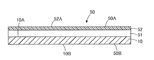
- a foldable light-transmitting optical film comprising a resin base material and a resin layer provided on the first surface side of the resin base material, wherein the resin base material has a thickness of 20 ⁇ m.
- the film thickness of the resin layer is 50 ⁇ m or more, and the ratio of the film thickness of the resin layer to the thickness of the resin substrate is 4.0 or more and 12.0 or less.
- the displacement amount of the resin base material is 50 nm or more and 250 nm or less, and the indentation test is performed on the cross section in the film thickness direction of the resin layer.
- An optical film in which the amount of displacement of the resin layer is 200 nm or more and 1500 nm or less.
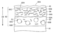
- a foldable optical film used in an image display device comprising a resin base material and a resin layer provided on one surface side of the resin base material and containing organic particles, wherein the resin The optical film, wherein the surface of the layer is an uneven surface, and the organic particles are unevenly distributed closer to the resin substrate than a center line that bisects the resin layer in the thickness direction of the resin layer.
- the resin substrate contains one or more resins selected from the group consisting of a polyimide resin, a polyamideimide resin, a polyamide resin, and a polyester resin. ..
- the resin layer includes a first resin layer and a second resin layer provided on the surface side of the first resin layer, and the first resin layer contains the organic particles.
- the optical film as described in any one of [11] to [14].
- the first aspect of the present invention it is possible to provide a resin layer having good foldability and good impact resistance, an optical film provided with the resin layer, and an image display device.
- the second aspect of the present invention it is possible to provide a foldable optical film which is hard to be bent and has good impact resistance, and an image display device including the same.
- the third aspect of the present invention it is possible to provide a foldable optical film in which pressing marks are less noticeable and which is less likely to break during folding, and an image display device including the foldable optical film.
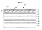
- FIG. 1 is a schematic configuration diagram of a resin layer according to the first embodiment.
- FIG. 2 is a partially enlarged view of the resin layer of FIG.
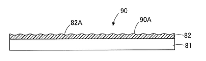
- FIG. 3 is a schematic configuration diagram of the optical film according to the first embodiment.
- 4 (A) to 4 (C) are diagrams schematically showing the state of the continuous folding test.
- FIG. 5 is a schematic configuration diagram of another optical film according to the first embodiment.
- FIG. 6 is a schematic configuration diagram of the image display device according to the first embodiment.
- FIG. 7 is a schematic configuration diagram of the optical film according to the second embodiment.
- FIG. 8(A) and FIG. 8(B) are diagrams schematically showing the state of the folding static test.
- FIG. 9 is a schematic configuration diagram of the optical film according to the third embodiment.
- FIG. 10 is a partially enlarged view of the optical film of FIG.
- FIG. 11 is a schematic configuration diagram of another optical film according to the third embodiment.
- FIG. 1 is a schematic configuration diagram of a resin layer according to the present embodiment
- FIG. 2 is a partially enlarged view of the resin layer of FIG. 1
- FIG. 3 is a schematic configuration diagram of an optical film according to the present embodiment.
- FIG. 4 is a diagram schematically showing a state of a continuous folding test
- FIG. 5 is a schematic configuration diagram of another optical film according to the embodiment.
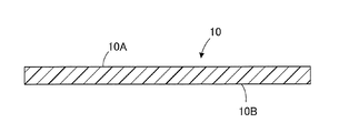
- the resin layer 10 shown in FIG. 1 is used in an image display device and has light transmittance.
- the "resin layer” in the present embodiment is a layer having a single-layer structure containing a resin.
- the resin layer 10 is made of a resin having a light transmitting property and has a shock absorbing property.
- the resin layer 10 may be used as a single resin layer 10, or may be used by being incorporated in the optical films 30 and 50 having a laminated structure.
- a release film may be attached to the resin layer 10.
- the "light transmissivity" in the present specification means a property of transmitting light, and for example, the total light transmittance is 50% or more, preferably 70% or more, more preferably 80% or more, particularly preferably 90%. Including the above.
- the light-transmissive property does not necessarily need to be transparent and may be semi-transparent.
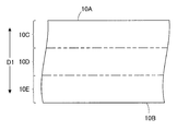
- the resin layer 10 divides the resin layer 10 into three equal parts in the film thickness direction D1 of the resin layer 10, and the first surface 10A to the first surface 10A of the resin layer 10 is opposite to the first surface 10A.
- the first region 10C, the second region 10D, and the third region 10E are formed in order toward the second surface 10B, and the first region 10C, the second region 10D, and the third region 10E are formed in the cross section of the resin layer 10 in the film thickness direction D1.
- the displacement amount in the first region 10C is d1
- the displacement amount in the second region 10D is d2
- the displacement amount in the third region 10E is d3, when the indentation test of pushing the Berkovich indenter with a constant load is performed, respectively.
- the relational expression (1) is satisfied. Since the resin layer of the present embodiment is softer than the functional layer (hard coat layer) and the resin base material described later and has a large effect of viscosity, the method of measuring the indentation hardness, the maltense hardness, etc. by the nanoindentation method is suitable. There wasn't. Therefore, the displacement amount is used as an index of hardness. d1 ⁇ d2 ⁇ d3 (1)
- the displacement amounts d1 to d3 can be obtained as follows using a nanoindenter (for example, TI950 TriboIndenter manufactured by Bruker). Specifically, first, a block in which a resin layer cut out to 1 mm ⁇ 10 mm is embedded with an embedding resin is prepared, and a uniform thickness of 70 nm or more and 100 nm without holes or the like is produced from this block by a general section preparation method. Cut out the following sections. Here, it was decided to cut out a section having a thickness of 70 nm or more and 100 nm or less because the remaining block from which the section was cut out was used at the time of measurement, but by cutting out a section having this thinness, the flatness of the cross section of the remaining block was used.
- a nanoindenter for example, TI950 TriboIndenter manufactured by Bruker.
- an ultramicrotome EM UC7 manufactured by Leica Microsystems Co., Ltd. can be used to prepare the slice. Then, the remaining block from which a uniform section having no holes or the like is cut out is used as a measurement sample. Then, in the cross section obtained by cutting out the section in such a measurement sample, a Berkovich indenter (triangular cone, for example, TI-0039 manufactured by Bruker) was used as the indenter under the following measurement conditions.
- the first region of the layer is vertically pushed into the center of the cross section in the thickness direction with a maximum load of 200 ⁇ N over 40 seconds, and the displacement amount (pushing depth) d1 at that time is measured.
- the Berkovich indenter is to be pushed into the portions apart from both side ends of the resin layer by 500 nm or more to the center side of the resin layer in order to avoid the influence of the side edges of the resin layer.
- the displacement amount is the arithmetic mean value of the values obtained by measuring at 10 points. If any of the measured values deviates from the arithmetic mean value by ⁇ 20% or more, the measured value shall be excluded and remeasurement shall be performed.
- Whether or not some measured values deviate from the arithmetic mean value by ⁇ 20% or more is determined by (A ⁇ B)/B ⁇ 100, where A is the measured value and B is the arithmetic mean value. Judgment shall be made based on whether the required value (%) is ⁇ 20% or more.
- the displacement amounts of the second region and the third region of the resin layer are also measured in the same manner as the displacement amount of the first region.
- the ratio of the displacement amount d1 to the displacement amount d3 is preferably 0.85 or less.
- d1 / d3 is 0.85 or less, both excellent foldability and impact resistance can be achieved at the same time.
- the upper limit of d1/d3 is more preferably 0.82 or less, or 0.80 or less, and the lower limit is 0.40 or more, 0.50 or less from the viewpoint of easily suppressing the generation of wrinkles during bending. It is preferably 0 or more, or 0.60 or more.
- the ratio (d1 / d2) of the displacement amount d1 to the displacement amount d2 is preferably 0.70 or more and 0.99 or less.
- d1/d2 is 0.70 or more, it is possible to suppress the generation of wrinkles during bending, and when d1/d2 is 0.99 or less, excellent foldability and impact resistance are obtained. It can be compatible.
- the lower limit of d1/d2 is more preferably 0.75 or more, 0.80 or more, or 0.85 or more, and the upper limit is 0.95 or less, 0.92 or less, or 0.90 or less. Is more preferable.
- the ratio (d2 / d3) of the displacement amount d2 to the displacement amount d3 is preferably 0.70 or more and 0.99 or less.
- d2/d3 is 0.70 or more, it is possible to suppress the occurrence of wrinkles during bending, and when d2/d3 is 0.99 or less, excellent foldability and impact resistance are obtained. It can be compatible.
- the lower limit of d2/d3 is more preferably 0.75 or more, 0.80 or more, or 0.85 or more, and the upper limit is 0.95 or less, 0.92 or less, or 0.90 or less. Is more preferable.
- the displacement amounts d1 to d3 are 1000 nm or less, respectively.
- the resin layer 10 has sufficient hardness and excellent impact resistance can be obtained.
- the upper limits of the displacement amounts d1 to d3 are more preferably 900 n ⁇ m or less, 800 nm or less, or 700 nm or less, and the lower limits are 200 nm or more, 300 nm or more, or 350 nm, respectively, from the viewpoint of ensuring the foldability of the resin layer 10. The above is more preferable.
- the total light transmittance of the resin layer 10 is preferably 85% or more. When the total light transmittance of the resin layer 10 is 85% or more, sufficient image visibility can be obtained when the resin layer 10 is used in a mobile terminal.
- the total light transmittance of the resin layer 10 is more preferably 87% or more, or 90% or more.
- the total light transmittance is measured using a haze meter (for example, product name "HM-150", manufactured by Murakami Color Research Laboratory Co., Ltd.) in an environment of a temperature of 23 ⁇ 5° C. and a relative humidity of 30% or more and 70% or less. It can be measured by a method based on JIS K7361-1: 1997.
- the total light transmittance is measured three times for one resin layer after cutting the resin layer into a size of 50 mm ⁇ 100 mm, setting it without curling or wrinkling, and without fingerprints or dust.
- the arithmetic mean value of the values obtained by measuring three times is used. In the present specification, “measuring three times” means not measuring the same place three times but measuring three different places.
- the first surface 10A and the second surface 10B visually observed are flat, and the variation in film thickness is within the range of ⁇ 10%. Therefore, it is considered that by measuring the total light transmittance at three different positions in the cut resin layer, an approximate average value of the total light transmittance of the entire surface of the resin layer can be obtained.
- the variation in the total light transmittance is within ⁇ 10% regardless of whether the measurement target is as long as 1 m ⁇ 3000 m or the size of a 5-inch smartphone. If the resin layer cannot be cut to the above size, for example, since the HM-150 has an inlet opening of 20 mm ⁇ for measurement, a sample size of 21 mm or more is required.
- the resin layer may be appropriately cut out to a size of 22 mm ⁇ 22 mm or more.
- the measurement points are set at three points by gradually shifting or changing the angle within a range in which the light source spot does not come off.
- the haze value (total haze value) of the resin layer 10 is preferably 3.0% or less. When the haze value of the resin layer is 3.0% or less, whitening of the image display surface can be suppressed when the resin layer is used for a mobile terminal.
- the haze value is more preferably 2.0% or less, 1.5% or less, 1.0% or less, or 0.5% or less.
- the haze value is JIS using a haze meter (for example, product name “HM-150”, manufactured by Murakami Color Research Laboratory Co., Ltd.) under the environment of temperature 23 ⁇ 5° C. and relative humidity 30% or more and 70% or less. It can be measured by a method based on K7136:2000. Specifically, the haze value is measured by the same method as the method for measuring the total light transmittance.
- a haze meter for example, product name “HM-150”, manufactured by Murakami Color Research Laboratory Co., Ltd.
- the thickness of the resin layer 10 is preferably 20 ⁇ m or more and 150 ⁇ m or less.
- the lower limit of the film thickness of the resin layer 10 is more preferably 40 ⁇ m or more, or 50 ⁇ m or more, and the upper limit of the resin layer 10 is suitable for thinning, and from the viewpoint of good workability, 120 ⁇ m or less, 100 ⁇ m or less, It is more preferably 80 ⁇ m or less, or 60 ⁇ m or less.
- the film thickness of the resin layer 10 As for the film thickness of the resin layer 10, a cross section of the resin layer 10 is photographed using a scanning electron microscope (SEM), and the film thickness of the resin layer 10 is measured at 10 positions in the image of the cross section. The arithmetic mean value of the film thickness.
- a block in which a resin layer cut out to a size of 1 mm ⁇ 10 mm is embedded with an embedding resin is prepared, and a uniform slice-free film having a thickness of 70 nm or more and 100 nm or less is formed from this block by a general method of preparing slices. Cut out a section.
- a uniform slice-free film having a thickness of 70 nm or more and 100 nm or less is formed from this block by a general method of preparing slices. Cut out a section.
- For the preparation of sections for example, Ultramicrotome EMUC7 manufactured by Leica Microsystems, Inc. can be used. Then, a uniform section without such holes is used as a measurement sample. After that, a cross-sectional photograph of the measurement sample is taken using a scanning transmission electron microscope (STEM).
- STEM scanning transmission electron microscope
- Examples of the scanning transmission electron microscope (STEM) include S-4800 manufactured by Hitachi High-Technologies Corporation.
- S-4800 manufactured by Hitachi High-Technologies Corporation.
- the cross-section is observed with the detector set to "SE”, the acceleration voltage set to "5 kV", and the emission current set to "10 ⁇ A".
- the contrast and the brightness are appropriately adjusted to 100 times to 100,000 times, preferably 500 times to 50,000 times, and more preferably 1000 times to 10,000 times. ..
- the beam monitor aperture is set to "3”
- the objective lens aperture is set to "3”
- W. D. May be set to "8 mm".
- the interface contrast between the resin layer and another layer (for example, the embedding resin) can be observed as clearly as possible when the cross-section is observed. If the interface is difficult to see due to insufficient contrast, dyeing treatment such as osmium tetroxide, ruthenium tetroxide, and phosphotungstic acid makes the interface between the organic layers easy to see. Further, it may be difficult to understand the interface contrast when the magnification is high. In that case, observe the low magnification at the same time.
- the above arithmetic mean value is obtained at both magnifications, and the average value is further calculated as the value of the film thickness of the resin layer.
- the resin constituting the resin layer 10 is not particularly limited as long as it is a resin such as Hz that satisfies the above relational expression (1).
- a resin include a cured product (polymer) of an ionizing radiation curable compound (ionizing radiation polymerizable compound).
- ionizing radiation in the present specification include visible light, ultraviolet light, X-ray, electron beam, ⁇ -ray, ⁇ -ray, and ⁇ -ray.
- Examples of the cured product of the ionizing radiation-curable compound include urethane resins and silicone resins.
- the urethane resin is a resin having a urethane bond.
- the urethane-based resin include a cured product of an ionizing radiation-curable urethane-based resin composition and a cured product of a thermosetting urethane-based resin composition.
- a cured product of an ionizing radiation curable urethane resin composition is preferable from the viewpoint of obtaining high hardness, fast curing speed, and excellent mass productivity.
- the ionizing radiation-curable urethane resin composition contains urethane (meth)acrylate, and the thermosetting urethane resin composition contains a polyol compound and an isocyanate compound.
- the urethane (meth) acrylate, polyol compound, and isocyanate compound may be any of a monomer, an oligomer, and a prepolymer.
- the number of (meth) acryloyl groups (number of functional groups) in the urethane (meth) acrylate is preferably 2 or more and 4 or less. If the number of (meth)acryloyl groups in the urethane (meth)acrylate is less than 2, the pencil hardness may be low, and if it exceeds 4, curing shrinkage becomes large and the optical film curls. Also, the resin layer may be cracked during bending.
- the upper limit of the number of (meth)acryloyl groups in the urethane (meth)acrylate is more preferably 3 or less.
- "(meth)acryloyl group” is meant to include both "acryloyl group” and "methacryloyl group”.
- the weight average molecular weight of urethane (meth)acrylate is preferably 1500 or more and 20000 or less. If the weight average molecular weight of the urethane (meth)acrylate is less than 1500, impact resistance may decrease, and if it exceeds 20,000, the viscosity of the ionizing radiation curable urethane-based resin composition increases and the coating There is a risk of deterioration of sex.
- the lower limit of the weight average molecular weight of urethane (meth) acrylate is more preferably 2000 or more, and the upper limit is more preferably 15000 or less.
- examples of the repeating unit having a structure derived from urethane (meth)acrylate include a structure represented by the following general formula (1), (2), (3) or (4).
- R 1 represents a branched alkyl group
- R 2 represents a branched alkyl group or a saturated cycloaliphatic group
- R 3 represents a hydrogen atom or a methyl group
- R 4 represents , Hydrogen atom, methyl group or ethyl group
- m indicates an integer of 0 or more
- x indicates an integer of 0 to 3.
- R 1 represents a branched alkyl group
- R 2 represents a branched alkyl group or a saturated cyclic aliphatic group
- R 3 represents a hydrogen atom or a methyl group
- R 4 represents a hydrogen atom or a methyl group.
- n represents an integer of 1 or more
- x represents an integer of 0 to 3.
- R 1 represents a branched alkyl group
- R 2 represents a branched alkyl group or a saturated cyclic aliphatic group
- R 3 represents a hydrogen atom or a methyl group
- R 4 represents a hydrogen atom or a methyl group.
- m indicates an integer of 0 or more
- x indicates an integer of 0 to 3.
- R 1 represents a branched alkyl group
- R 2 represents a branched alkyl group or a saturated cycloaliphatic group
- R 3 represents a hydrogen atom or a methyl group
- R 4 represents ,
- n represents an integer of 1 or more
- x represents an integer of 0 to 3.
- the structure of the resin constituting the resin layer 10 is formed by polymer chains (repeating units), for example, pyrolysis gas chromatograph mass spectrometry (GC-MS) and Fourier transform infrared spectroscopy. It can be determined by analyzing the resin layer 10 by the method (FT-IR). Pyrolysis GC-MS is particularly useful because the monomer unit contained in the resin layer 10 can be detected as a monomer component.
- GC-MS pyrolysis gas chromatograph mass spectrometry
- FT-IR Fourier transform infrared spectroscopy
- the resin layer 10 may include an ultraviolet absorber, a spectral transmittance adjuster, an antifouling agent, inorganic particles and/or organic particles, etc., in addition to the resin.
- the optical film 30 shown in FIG. 3 is a film having a laminated structure, and includes at least a resin layer 10.
- the optical film 30 further includes a functional layer 31 provided on one of the first surface 10A and the second surface 10B of the resin layer 10.
- the "functional layer” in this specification is a layer that exhibits some function.
- the functional layer 31 has a single-layer structure, but may have a multilayer structure of two or more layers.
- the optical film 30 does not have a base material.
- the optical film 30 is foldable. Specifically, under the environment of temperature 23 ⁇ 5° C. and relative humidity of 30% or more and 70% or less, a folding test (continuous folding test) described below for the optical film 30 is performed 100,000 times, 200,000 times, 50 times. It is preferable that the optical film 30 does not crack or break even when it is repeated 10,000 times or 1 million times. When the optical film 30 is repeatedly subjected to the continuous folding test 100,000 times and the optical film 30 is cracked or fractured, the foldability of the optical film 30 becomes insufficient.
- the number of times of folding in the continuous folding test is evaluated at least 100,000 times for the following reasons. For example, assuming that the optical film is incorporated into a foldable smartphone, the frequency of folding (the frequency of opening and closing) becomes extremely high.
- the number of times of folding in the continuous folding test is, for example, 10,000 or 50,000
- the evaluation that the number of foldings is 10,000 times in the continuous folding test means that only a level that cannot be used as a product can be confirmed. Therefore, in order to evaluate whether or not it is at a practical level, it is necessary to evaluate the number of foldings in the continuous folding test at least 100,000. It is more preferable that the bent portion does not deform when a continuous folding test is performed on the optical film 30.
- the continuous folding test may be performed so as to fold the optical film 30 so that the surface 30A is on the outside, or may be performed so that the optical film 30 is so that the surface 30A is on the inside. Even in this case, it is preferable that the optical film 30 does not crack or break.
- the continuous folding test is performed as follows. In the continuous folding test as shown in FIG. 4(A), first, a sample S having a size of 30 mm ⁇ 100 mm is cut out from the optical film 30. When the sample S having a size of 30 mm ⁇ 100 mm cannot be cut out from the optical film 30, the sample S may be cut out to have a size of 10 mm ⁇ 100 mm, for example.
- a side edge S1 of the cut out sample S and a side edge S2 opposed to the side edge S1 are arranged in parallel to each other, and a folding endurance tester (for example, product name “U-shaped expansion/contraction tester DLDMLH-FS”, Yuasa It is fixed by fixing parts 40 and 45 of IEC 62715-6-1 manufactured by System Equipment Co., Ltd., respectively. Fixing by the fixing portions 40 and 45 is performed by holding a portion of the sample S having a length of about 10 mm on one side in the longitudinal direction of the sample S.
- a folding endurance tester for example, product name “U-shaped expansion/contraction tester DLDMLH-FS”, Yuasa It is fixed by fixing parts 40 and 45 of IEC 62715-6-1 manufactured by System Equipment Co., Ltd., respectively. Fixing by the fixing portions 40 and 45 is performed by holding a portion of the sample S having a length of about 10 mm on one side in the longitudinal direction of the sample S.
- the portion of the sample S required for this fixing is up to about 20 mm, it can be measured by attaching it to the fixing portions 40 and 45 with a tape. Further, as shown in FIG. 4(A), the fixed portion 40 is slidable in the horizontal direction. Note that the above-mentioned device is preferable, unlike the conventional method of winding a sample around a rod, etc., because it is possible to evaluate durability against bending load without generating tension or friction in the sample.
- the fixing part 40 is moved so as to be close to the fixing part 45, thereby deforming the central portion of the sample S so as to be folded, and further, as shown in FIG. 4(C).
- the fixing part 40 is moved in the opposite direction. It is moved to eliminate the deformation of the optical film 30.
- the central portion of the sample S can be folded by 180 °. Further, the bent portion S3 of the sample S is prevented from protruding from the lower ends of the fixing portions 40 and 45, and a continuous folding test is performed under the following conditions, and the interval ⁇ when the fixing portions 40 and 45 are closest to each other is controlled. By doing so, the interval ⁇ between the two opposite side portions S1 and S2 of the sample S can be set to 10 mm. In this case, the outer diameter of the bent portion S3 is considered to be 10 mm.
- the surface 30A of the optical film 30 (the surface 31A of the functional layer 31) has a hardness (pencil hardness) of 3H or more when measured by a pencil hardness test specified in JIS K5600-5-4:1999. It is preferably 4H or more, and more preferably 4H or more.
- the optical film 30 cut into a size of 30 mm ⁇ 100 mm is fixed on a glass plate with Cellotape (registered trademark) manufactured by Nichiban Co., Ltd. so as not to be bent or wrinkled, and the temperature is 23 ⁇ 5° C. and relative humidity.
- a pencil hardness tester for the surface 30A of the optical film 30 in an environment of 30% or more and 70% or less for example, product name "pencil scratch coating hardness tester (electric type)", manufactured by Toyo Seiki Seisakusho Co., Ltd.
- the pencil for example, product name “Uni”, manufactured by Mitsubishi Pencil Co., Ltd.
- the pencil hardness is the highest hardness that does not scratch the surface of the optical film in the pencil hardness test.
- a plurality of pencils having different hardness are used.
- the pencil hardness test is performed 5 times for each pencil, and the surface of the optical film is scratched 4 times or more out of 5 times. If not, it is judged that the surface of the optical film was not scratched with the pencil of this hardness.
- the scratches refer to those that are visually observed by transmitting and observing the surface of an optical film subjected to a pencil hardness test under a fluorescent lamp.
- the total light transmittance of the optical film 30 is preferably 85% or more, and more preferably 87% or more, 88% or more, or 90% or more for the same reason as described in the section of the resin layer 10. preferable.
- the total light transmittance of the optical film 30 is measured by the same method as the method of measuring the total light transmittance of the resin layer 10.
- the haze value (total haze value) of the optical film 30 is preferably 3.0% or less, 2.0% or less, 1.5% or less, for the same reason as described in the section of the resin layer 10. It is more preferably 1.0% or less or 0.5% or less.
- the haze value of the optical film 30 is measured by the same method as the method for measuring the haze value of the resin layer 10.
- optical film 30 is not particularly limited, but examples of the use of the optical film 30 include image display devices such as smartphones, tablet terminals, personal computers (PC), wearable terminals, digital signage, televisions, and car navigations. Can be mentioned. Further, the optical film 30 is also suitable for in-vehicle use. The form of each of the image display devices described above is also preferable for applications requiring flexibility such as foldable and rollable.
- the optical film 30 may be cut into a desired size, or may be roll-shaped.
- the size of the optical film is not particularly limited and is appropriately determined according to the size of the display surface of the image display device.
- the size of the optical film 30 may be, for example, 2.8 inches or more and 500 inches or less.
- “inch” means the length of a diagonal line when the optical film has a quadrangular shape, the diameter when the optical film has a circular shape, and the minor axis when the optical film has an elliptical shape. And mean the major axis.
- the aspect ratio of the optical film when determining the inch is not particularly limited as long as there is no problem as a display screen of the image display device.
- vertical: horizontal 1: 1, 4: 3, 16:10, 16: 9, 2: 1 and the like.
- the aspect ratio is not limited to this, especially in in-vehicle applications and digital signage, which are rich in design.
- the size of the optical film 30 is large, it is cut out to an A5 size (148 mm ⁇ 210 mm) from an arbitrary position and then cut out to the size of each measurement item.
- the optical film 30 is in a roll shape, it is not an ineffective region including both end portions extending along the longitudinal direction of the roll, while paying out a predetermined length from the roll of the optical film 30, The desired size is cut out from the effective area near the center where the quality is stable.
- the location of the optical film 30 in the image display device may be inside the image display device, but it is preferably near the surface of the image display device.
- the optical film 30 When used near the surface of an image display device, the optical film 30 functions as a cover film (window film) used in place of the cover glass.
- the functional layer 31 is preferably provided on the first surface 10A side of the resin layer 10, that is, on the first region 10C side. By providing the functional layer 31 on the side of the first region 10C in this way, the scratch resistance is excellent and the excellent foldability is not impaired.
- the functional layer 31 shown in FIG. 3 is a layer mainly for imparting hardness to the optical film 30, and specifically, a layer functioning as a hard coat layer.
- the functional layer 31 may be a layer having another function.
- the “hard coat layer” in the present embodiment means a layer having a Martens hardness (HM) at the center of the cross section of the functional layer of 375 MPa or more.
- HM Martens hardness
- the "Martens hardness” in the present specification is the hardness when the indenter is pressed by 500 nm by the hardness measurement by the nanoindentation method.
- the measurement of the Martens hardness by the nanoindentation method shall be carried out using "TI950 TriboIndenter” manufactured by Bruker Co., Ltd.
- a Berkovich indenter (triangular pyramid, for example, TI-0039 manufactured by Bruker) is pushed as the indenter by 500 nm perpendicular to the cross section of the functional layer.
- the Berkovich indenter is 500 nm away from the interface between the resin layer and the functional layer to the center side of the functional layer, and the center of the functional layer from both ends of the functional layer. It shall be pushed into the portion of the functional layer that is 500 nm or more away from the side.
- the Martens hardness shall be the arithmetic mean value of the values obtained by measuring 10 points. If any of the measured values deviates from the arithmetic mean value by ⁇ 20% or more, the measured value shall be excluded and remeasurement shall be performed. Whether or not any of the measured values deviates from the arithmetic mean value by ⁇ 20% or more depends on (AB) / B ⁇ 100 when the measured value is A and the arithmetic mean value is B.
- Judgment shall be made based on whether the required value (%) is ⁇ 20% or more.
- (Measurement condition) ⁇ Control method: Displacement control ⁇ Load speed: 10 nm / sec ⁇ Holding time: 5 seconds ⁇ Load unloading speed: 10 nm / sec ⁇ Measurement temperature: 23 ⁇ 5 ° C ⁇ Measured humidity: 30% to 70%
- the Martens hardness of the functional layer 31 is preferably 375 MPa or more and 1500 MPa or less. If the Martens hardness of the functional layer 31 is 375 MPa or more, good hardness can be obtained, and if it is 1500 MPa or less, good folding performance can be obtained.
- the film thickness of the functional layer 31 is preferably 3 ⁇ m or more and 10 ⁇ m or less.
- the “film thickness of the functional layer” means the film thickness (total thickness) obtained by summing the film thicknesses of the functional layers when the functional layer has a multilayer structure.
- the lower limit of the film thickness of the functional layer 31 is more preferably 4 ⁇ m or more or 5 ⁇ m or more, and the upper limit is more preferably 8 ⁇ m or less or 7 ⁇ m or less.
- the film thickness of the functional layer 31 As for the film thickness of the functional layer 31, a cross section of the functional layer 31 is photographed using a scanning transmission electron microscope (STEM) or a transmission electron microscope (TEM), and the film thickness of the functional layer 31 is shown in the image of the cross section. The measurement is performed at 10 points, and the arithmetic average value of the film thickness at the 10 points is used.
- STEM scanning transmission electron microscope
- TEM scanning transmission electron microscope
- the cross section is observed with the detector set to "TE", the acceleration voltage set to "30 kV", and the emission current set to "10 ⁇ A".
- the magnification the focus is adjusted, and the contrast and brightness are appropriately adjusted from 5000 times to 200,000 times while observing whether each layer can be distinguished.
- a preferred magnification is 10,000 to 100,000 times, a more preferred magnification is 10,000 to 50,000 times, and a most preferred magnification is 25,000 to 50,000 times.
- the beam monitor aperture is set to "3”
- the objective lens aperture is set to "3”
- the interface contrast between the functional layer and another layer (for example, a resin layer) can be observed as clearly as possible when the cross-section is observed. If the interface is difficult to see due to insufficient contrast, dyeing treatment such as osmium tetroxide, ruthenium tetroxide, and phosphotungstic acid makes the interface between the organic layers easy to see. Further, it may be difficult to understand the interface contrast when the magnification is high. In that case, observe the low magnification at the same time.
- the arithmetic mean value described above is obtained at both magnifications, and the average value is further calculated for the functional layer. It is the value of the film thickness.
- the functional layer 31 preferably further contains a resin and inorganic particles dispersed in the resin.
- the resin contains a polymer (cured product) of a polymerizable compound (curable compound).
- the polymerizable compound has at least one polymerizable functional group in the molecule.
- the polymerizable functional group include ethylenically unsaturated groups such as (meth) acryloyl group, vinyl group and allyl group.
- polyfunctional (meth)acrylate is preferable.
- the polyfunctional (meth)acrylate include trimethylolpropane tri(meth)acrylate, tripropylene glycol di(meth)acrylate, diethylene glycol di(meth)acrylate, dipropylene glycol di(meth)acrylate, pentaerythritol tri( (Meth)acrylate, pentaerythritol tetra(meth)acrylate, dipentaerythritol hexa(meth)acrylate, 1,6-hexanediol di(meth)acrylate, neopentyl glycol di(meth)acrylate, ditrimethylolpropane tetra(meth)acrylate , Dipentaerythritol penta(meth)acrylate, tripentaerythritol octa(meth)acrylate, tetrapentaerythritol deca
- trifunctional to hexafunctional compounds are preferable because they can suitably satisfy the above-mentioned Martens hardness, and examples thereof include pentaerythritol triacrylate (PETA), dipentaerythritol hexaacrylate (DPHA), and pentaerythritol tetraacrylate (PETTA). ), dipentaerythritol pentaacrylate (DPPA), trimethylolpropane tri(meth)acrylate, tripentaerythritol octa(meth)acrylate, tetrapentaerythritol deca(meth)acrylate and the like are preferable.
- (meth) acrylate means acrylate and methacrylate.
- a monofunctional (meth) acrylate monomer may be further contained in order to adjust the hardness and viscosity of the composition, improve the adhesion, and the like.
- the monofunctional (meth)acrylate monomer include hydroxyethyl acrylate (HEA), glycidyl methacrylate, methoxypolyethylene glycol (meth)acrylate, isostearyl (meth)acrylate, 2-acryloyloxyethyl succinate, acryloylmorpholine and N.
- the weight average molecular weight of the monomer is preferably less than 1000, more preferably 200 or more and 800 or less, from the viewpoint of improving the hardness of the resin layer.
- the weight average molecular weight of the polymerizable oligomer is preferably 1,000 or more and 20,000 or less, more preferably 1,000 or more and 10,000 or less, and even more preferably 2,000 or more and 7,000 or less.
- the inorganic particles are not particularly limited as long as the hardness can be improved, but silica particles are preferable from the viewpoint of obtaining excellent hardness.
- silica particles reactive silica particles are preferable.
- the reactive silica particles are silica particles capable of forming a cross-linked structure with the polyfunctional (meth)acrylate, and by containing the reactive silica particles, the hardness of the functional layer 31 is sufficiently high. Can be enhanced to.
- the above-mentioned reactive silica particles preferably have a reactive functional group on the surface thereof.
- the reactive functional group for example, the above-mentioned polymerizable functional group is preferably used.
- the above-mentioned reactive silica particles are not particularly limited, and conventionally known ones can be used, and examples thereof include the reactive silica particles described in JP-A-2008-165040.
- Examples of commercially available reactive silica particles include MIBK-SD, MIBK-SD-MS, MIBK-SD-L, MIBK-SD-ZL (all manufactured by Nissan Chemical Industries, Ltd.) and V8802, Examples thereof include V8803 (both manufactured by Nissan Chemical Industries, Ltd.).
- the silica particles may be spherical silica particles, but are preferably deformed silica particles.
- the spherical silica particles and the irregularly shaped silica particles may be mixed.
- the “spherical silica particles” mean, for example, silica particles having a perfect sphere shape, an elliptic sphere shape, or the like, and “heteromorphic silica particles” have a potato-like shape (the aspect ratio at the time of cross-section observation is 1 .2 or more and 40 or less) means a silica particle having a shape having random irregularities on the surface.
- the surface area of the irregularly shaped silica particles is larger than that of the spherical silica particles, by containing such irregularly shaped silica particles, the contact area with the polyfunctional (meth)acrylate or the like becomes large, and the hard coat The hardness of the layer can be improved.
- Whether the silica particles contained in the functional layer are irregular-shaped silica particles can be confirmed by observing the cross section of the functional layer with a transmission electron microscope (TEM) or a scanning transmission electron microscope (STEM). it can.
- TEM transmission electron microscope
- STEM scanning transmission electron microscope
- the average particle size of the silica particles is preferably 5 nm or more and 200 nm or less.
- the average particle size of the silica particles is 5 nm or more, the production of the particles themselves is not difficult, the agglomeration of the particles can be suppressed, and it is not difficult to make the particles into irregular shapes.
- the average particle size of the irregular-shaped silica particles is 200 nm or less, it is possible to suppress the formation of large irregularities in the functional layer and also suppress the increase in haze.
- the average particle size of the silica particles is 20 particles from the image of the cross section of the particles photographed using a transmission electron microscope (TEM) or a scanning transmission electron microscope (STEM). The particle size of is measured and the arithmetic mean value of the particle sizes of 20 particles is taken.
- the average particle size of the silica particles is determined by using a transmission electron microscope (TEM) or a scanning transmission electron microscope (STEM) to obtain an image of a cross section of the hard coat layer.
- the maximum value (major axis) and the minimum value (minor axis) of the distance between two points on the outer circumference of the particle are measured and averaged to obtain the particle diameter, which is taken as the arithmetic average value of the particle diameters of 20 particles.
- the hardness (Martens hardness) of the functional layer 31 can be controlled by controlling the size and blending amount of the inorganic particles.
- the silica particles when the functional layer 31 is formed, the silica particles have a diameter of 5 nm or more and 200 nm or less, and preferably 25 to 60 parts by mass with respect to 100 parts by mass of the polymerizable compound.
- the functional layer 31 may include a material other than the above-mentioned materials within a range that satisfies the above-mentioned Martens hardness, and, for example, as a resin component material, a polymerizable monomer that forms a cured product by irradiation with ionizing radiation, It may contain a polymerizable oligomer and the like.
- a resin component material a polymerizable monomer that forms a cured product by irradiation with ionizing radiation
- It may contain a polymerizable oligomer and the like.
- the polymerizable monomer or polymerizable oligomer include (meth)acrylate monomers having a radical polymerizable unsaturated group in the molecule, or (meth)acrylate oligomers having a radical polymerizable unsaturated group in the molecule.
- the (meth)acrylate monomer having a radical polymerizable unsaturated group in the molecule or the (meth)acrylate oligomer having a radical polymerizable unsaturated group in the molecule include, for example, urethane (meth)acrylate and polyester (meth).
- Monomers or oligomers such as acrylate, epoxy (meth)acrylate, melamine (meth)acrylate, polyfluoroalkyl (meth)acrylate, and silicone (meth)acrylate.
- These polymerizable monomers or polymerizable oligomers may be used alone or in combination of two or more. Among them, polyfunctional (six or more functional) and urethane (meth)acrylate having a weight average molecular weight of 1,000 to 10,000 are preferable.
- the functional layer 31 may further contain an ultraviolet absorber, a spectral transmittance adjusting agent, and / or an antifouling agent.
- the optical film 30 shown in FIG. 3 does not have a base material, but may have a base material like the optical film 50 shown in FIG.
- the optical film 50 includes a resin layer 10, a resin base material 51, and a functional layer 52 in this order.
- the resin base material 51 is preferably provided on the first surface 10A side of the resin layer 10.
- the resin layer 10 is directly provided on the resin base material 51, but may be attached to the resin base material via an adhesive layer.
- the surface 50A of the optical film 50 is the surface 52A of the functional layer 52.
- the surface of the optical film is used to mean the surface on one side of the optical film, and the surface opposite to the surface of the optical film is referred to as the back surface to distinguish it from the surface of the optical film.
- the back surface 50B of the optical film 50 is the second surface 10B of the resin layer 10.
- the optical film 50 is also foldable like the optical film 30.
- the preferable number of folds, the preferable interval ⁇ between the opposite sides, and the conditions for the continuous fold test are the same as those for the optical film 30, and thus the description thereof is omitted here.
- the surface 50A of the optical film 50 may have a hardness (pencil hardness) of 2B or more when measured by the pencil hardness test specified in JIS K5600-5-4:1999. preferable.
- the pencil hardness of the optical film 50 is measured by the same method as the pencil hardness of the optical film 30.
- the optical film 50 preferably has a yellow index (YI) of 15 or less.
- YI yellow index
- the upper limit of the yellow index (YI) of the optical film 50 is more preferably 10 or less, 5 or less, or 1.5 or less.
- the Yellow Index (YI) is a spectrophotometer (for example, product name "UV-2450", manufactured by Shimadzu Corporation, light source: tungsten lamp and under the environment of temperature 23 ⁇ 5 ° C. and relative humidity 30% or more and 70% or less.
- Deuterium lamp 50 mm x 100 mm size cut out from the optical film resin layer side of the optical film is arranged so that the light source side, measured from the transmittance of the optical film wavelength 300nm ⁇ 780nm described in JIS Z8722:2009
- the chromaticity tristimulus values X, Y, and Z are calculated according to the calculated formula, and the values are calculated from the tristimulus values X, Y, and Z according to the calculation formula described in ASTM D1925:1962.
- the upper limit of the yellow index (YI) of the optical film 50 is more preferably 10 or less.
- the yellow index (YI) is measured three times for one optical film, and is used as an arithmetic mean value of the values obtained by measuring the three times.
- the yellow index is calculated by reading the above-mentioned transmittance measurement data on a monitor connected to UV-2450 and checking the item "YI" in the calculation items. ..
- the transmittance at a wavelength of 300 nm to 780 nm shall be determined by measuring the transmittance for at least 5 points between the front and rear 1 nm at a wavelength of 300 nm to 780 nm and calculating the average value under the following conditions. .. Further, if undulations appear in the spectrum of the spectral transmittance, the smoothing process may be performed with a delta of 5.0 nm.
- the total light transmittance of the optical film 50 is preferably 85% or more, and more preferably 87% or more, or 90% or more for the same reason as described in the section of the resin layer 10.
- the total light transmittance of the optical film 50 is measured by the same method as the method of measuring the total light transmittance of the resin layer 10.
- the haze value (total haze value) of the optical film 50 is preferably 3.0% or less, 2.0% or less, 1.5% or less, for the same reason as described in the section of the resin layer 10. It is more preferably 1.0% or less or 0.5% or less.
- the haze value of the optical film 50 is measured by the same method as the method for measuring the haze value of the resin layer 10.
- the resin base material 51 has optical transparency.
- the resin base material 51 is, for example, one or more resins selected from the group consisting of polyimide-based resins, polyamideimide-based resins, polyamide-based resins, and polyester-based resins (for example, polyethylene terephthalate resin and polyethylene naphthalate resin). It is preferable to include it.
- a polyimide resin, a polyamide resin, or a mixture thereof is preferable.
- the polyimide resin is obtained by reacting a tetracarboxylic acid component and a diamine component.
- the polyimide-based resin is not particularly limited, but is selected from the group consisting of structures represented by the following general formula (5) and the following general formula (7), for example, from the viewpoint of having excellent light transmittance and excellent rigidity. It is preferable to have at least one structure.
- R 5 is a tetravalent group which is a tetracarboxylic acid residue
- R 6 is a trans-cyclohexanediamine residue, trans-1,4-bismethylenecyclohexanediamine residue, 4,4.
- tetracarboxylic acid residue means a residue obtained by removing four carboxyl groups from tetracarboxylic acid, and a residue obtained by removing an acid dianhydride structure from tetracarboxylic dianhydride. Represents the same structure.
- diamine residue refers to a residue obtained by removing two amino groups from diamine.
- R 7 and R 8 independently represent a hydrogen atom, an alkyl group, or a perfluoroalkyl group.
- R 9 is a cyclohexanetetracarboxylic acid residue, a cyclopentanetetracarboxylic acid residue, a dicyclohexane-3,4,3', 4'-tetracarboxylic acid residue, and 4,4'.
- -At least one tetravalent group selected from the group consisting of (hexafluoroisopropyridene) diphthalic acid residues R 10 represents a divalent group which is a diamine residue.
- n′ represents the number of repeating units and is 1 or more.
- R 5 is a tetracarboxylic acid residue, and can be a residue obtained by removing the acid dianhydride structure from the tetracarboxylic dianhydride as exemplified above.
- the R 5 in formula (5) among others, from the viewpoint of improving optical transparency, and to improve the rigidity, 4,4 '- (hexafluoro isopropylidene) diphthalic acid residue, 3,3', 4,4'-biphenyltetracarboxylic acid residue, pyromellitic acid residue, 2,3', 3,4'-biphenyltetracarboxylic acid residue, 3,3', 4,4'-benzophenone tetracarboxylic acid residue Group, 3,3',4,4'-diphenylsulfone tetracarboxylic acid residue, 4,4'-oxydiphthalic acid residue, cyclohexanetetracarboxylic acid residue, and cyclopenta
- the total amount of these suitable residues is preferably 50 mol% or more, more preferably 70 mol% or more, still more preferably 90 mol% or more.
- R 5 3,3 ', 4,4'-biphenyltetracarboxylic acid residue, 3,3', from the group consisting of 4,4'-benzophenone tetracarboxylic acid residue and a pyromellitic acid residue
- a mixture with a tetracarboxylic acid residue group (group B) suitable for improving transparency such as at least one kind selected from the group consisting of pentane tetracarboxylic acid residues.
- the content ratio of the tetracarboxylic acid residue group (group A) suitable for improving the rigidity and the tetracarboxylic acid residue group (group B) suitable for improving transparency is: 0.05 mol of a tetracarboxylic acid residue group (group A) suitable for improving the rigidity, relative to 1 mol of a tetracarboxylic acid residue group (group B) suitable for improving transparency. It is preferably 9 mol or more, more preferably 0.1 mol or more and 5 mol or less, and further preferably 0.3 mol or more and 4 mol or less.
- the R 6 in formula (5) among others, from the viewpoint of improving optical transparency, and to improve the rigidity, 4,4'-diaminodiphenyl sulfone residue, 3,4'-diaminodiphenyl sulfone residues , And at least one divalent group selected from the group consisting of divalent groups represented by the above general formula (6), and further, 4,4'-diaminodiphenylsulfone residues, 3 , 4'-diaminodiphenyl sulfone residue, and at least one divalent selected from the group consisting of divalent groups R 7 and R 8 is represented by the general formula is a perfluoroalkyl group (6) It is preferably the basis of.
- the R 9 in the general formula (7) preferably contains 4,4'-diphenylsulfone tetracarboxylic acid residues and oxydiphthalic acid residues.
- these suitable residues are preferably contained in an amount of 50 mol% or more, more preferably 70 mol% or more, and further preferably 90 mol% or more.
- R 10 in the above general formula (7) is a diamine residue, and can be a residue obtained by removing two amino groups from the diamine as exemplified above.
- the R 10 in the general formula (7) among others, from the viewpoint of improving optical transparency, and to improve the rigidity, 2,2'-bis (trifluoromethyl) benzidine residues, bis [4- (4 -Aminophenoxy)phenyl]sulfone residue, 4,4'-diaminodiphenylsulfone residue, 2,2-bis[4-(4-aminophenoxy)phenyl]hexafluoropropane residue, bis[4-(3- Aminophenoxy) phenyl] sulfone residue, 4,4'-diamino-2,2'-bis (trifluoromethyl) diphenyl ether residue, 1,4-bis [4-amino-2- (trifluoromethyl) phenoxy] Benzene residue, 2,2-bis[4-(4-a
- It preferably contains one divalent group, plus 2,2'-bis (trifluoromethyl) benzidine residues, bis [4- (4-aminophenoxy) phenyl] sulfone residues, and 4,4. It preferably contains at least one divalent group selected from the group consisting of'-diaminodiphenyl sulfone residues.
- the total amount of these suitable residues is preferably 50 mol% or more, more preferably 70 mol% or more, still more preferably 90 mol% or more.
- R 10 a bis [4- (4-aminophenoxy) phenyl] sulfone residue, a 4,4'-diaminobenzanilide residue, an N, N'-bis (4-aminophenyl) terephthalamide residue,
- a group of diamine residues suitable for improving rigidity such as at least one selected from the group consisting of paraphenylenediamine residues, metaphenylenediamine residues, and 4,4'-diaminodiphenylmethane residues.
- the content ratio of the diamine residue group (group C) suitable for improving the rigidity and the diamine residue group (group D) suitable for improving the transparency improves transparency.
- the diamine residue group (group C) suitable for improving the rigidity is 0.05 mol or more and 9 mol or less with respect to 1 mol of the diamine residue group (group D) suitable for The amount is more preferably 0.1 mol or more and 5 mol or less, and further preferably 0.3 mol or more and 4 mol or less.
- n and n'independently represent the number of repeating units and are 1 or more.
- the number of repeating units n in the polyimide may be appropriately selected according to the structure so as to show a preferable glass transition temperature described later, and is not particularly limited.
- the average number of repeating units is usually 10 to 2000, preferably 15 to 1000.
- the polyimide resin may contain a polyamide structure as a part thereof.
- examples of the polyamide structure that may be included include a polyamideimide structure containing a tricarboxylic acid residue such as trimellitic anhydride, and a polyamide structure containing a dicarboxylic acid residue such as terephthalic acid.
- the polyimide resin preferably has a glass transition temperature of 250° C. or higher, and more preferably 270° C. or higher.
- the glass transition temperature is preferably 400° C. or lower, and more preferably 380° C. or lower, from the viewpoint of ease of stretching and reduction of the baking temperature.
- polyimide resin examples include compounds having a structure represented by the following chemical formula.
- n is a repeating unit and represents an integer of 2 or more.
- a polyimide-based resin or a polyamide-based resin having a structure in which intramolecular or intermolecular charge transfer is unlikely to occur is preferable because it has excellent transparency, and specifically, the chemical formula (8) above.
- examples thereof include fluorinated polyimide resins such as (15) to (15), and polyimide resins having an alicyclic structure such as the above formulas (15) to (19).
- the fluorinated polyimide-based resins represented by the chemical formulas (8) to (15) have high heat resistance because they have a fluorinated structure, and the heat generated during the production of the polyimide film made of the polyimide-based resin is high. Since it is not colored by, it has excellent transparency.
- Polyamide-based resin is a concept that includes not only aliphatic polyamide but also aromatic polyamide (aramid).
- examples of the polyamide resin include compounds having a skeleton represented by the following chemical formulas (25) to (27).
- n is a repeating unit and represents an integer of 2 or more.
- a commercially available material may be used as the base material made of the polyimide resin or polyamide resin represented by the chemical formulas (8) to (24) and (27).
- Examples of commercial products of the base material containing the polyimide-based resin include, for example, Neoprim (registered trademark) manufactured by Mitsubishi Gas Chemical Co., Inc., and commercial products of the base material containing the polyamide-based resin include, for example, Toray. Examples include Miktron (registered trademark) manufactured by the company.
- polyimide-based resin or polyamide-based resin represented by the above chemical formulas (8) to (24) and (27) those synthesized by a known method may be used.
- a method for synthesizing the polyimide resin represented by the chemical formula (8) is described in JP-A-2009-132091, and specifically, 4,4′-hexa represented by the chemical formula (28) below is represented. It can be obtained by reacting fluoropropylidene bisphthalic acid dianhydride (FPA) with 2,2′-bis(trifluoromethyl)-4,4′-diaminobiphenyl (TFDB).
- FPA fluoropropylidene bisphthalic acid dianhydride
- TFDB 2,2′-bis(trifluoromethyl)-4,4′-diaminobiphenyl
- the weight average molecular weight of the polyimide-based resin or polyamide-based resin is preferably in the range of 3,000 or more and 500,000 or less, more preferably in the range of 5,000 or more and 300,000 or less, and in the range of 10,000 or more and 200,000 or less. More preferably, When the weight average molecular weight is less than 3,000, sufficient strength may not be obtained, and when it exceeds 500,000, viscosity increases and solubility decreases, so that a substrate having a smooth surface and a uniform film thickness is obtained. Sometimes you can't get it.
- the "weight average molecular weight” is a polystyrene-equivalent value measured by gel permeation chromatography (GPC).
- the resin base material 51 is a fluorinated polyimide resin represented by the chemical formulas (8) to (15) or the like or a polyamide group having a halogen group represented by the chemical formula (27) or the like from the viewpoint of improving hardness. It is preferable to use a base material made of resin. Above all, it is more preferable to use a base material containing the polyimide resin represented by the chemical formula (8) from the viewpoint that the hardness can be further improved.
- polyester resins include resins having at least one of polyethylene terephthalate, polypropylene terephthalate, polybutylene terephthalate, and polyethylene naphthalate as a constituent component.
- the thickness of the resin base material 51 is preferably 10 ⁇ m or more and 100 ⁇ m or less.
- the thickness of the resin base material 51 is 10 ⁇ m or more, curling of the optical film can be suppressed and sufficient hardness can be obtained. Furthermore, even when the optical film is manufactured by Roll to Roll, wrinkles do not occur. It is less likely to occur, and there is no fear that the appearance will deteriorate.
- the thickness of the resin base material 51 is 100 ⁇ m or less, the folding performance of the optical film 50 is good, the requirements of the continuous folding test can be satisfied, and the weight reduction of the optical film 50 is preferable. ..
- the thickness of the resin base material 51 can be measured by the same method as the thickness of the resin layer 10.
- the lower limit of the resin base material 51 is more preferably 20 ⁇ m or more, 30 ⁇ m or more, or 40 ⁇ m or more, and the upper limit of the resin base material 51 is more preferably 80 ⁇ m or less, or 50 ⁇ m or less.
- the resin layer 10 and the optical films 30 and 50 can be manufactured as follows.
- the composition for the resin layer is applied onto one surface of the release film by a coating device such as a bar coater to form a coating film.
- the resin layer composition contains at least an ionizing radiation-curable compound.
- it may further contain a solvent and a polymerization initiator.
- the ionizing radiation-curable compound has been described in the section of the resin layer 10, and thus the description thereof will be omitted here.
- solvent examples include alcohols (eg, methanol, ethanol, propanol, isopropanol, n-butanol, s-butanol, t-butanol, benzyl alcohol, PGME, ethylene glycol, diacetone alcohol), ketones (eg, acetone, methyl ethyl ketone, Methyl isobutyl ketone, cyclopentanone, cyclohexanone, heptanone, diisobutyl ketone, diethyl ketone, diacetone alcohol), ester (methyl acetate, ethyl acetate, butyl acetate, n-propyl acetate, isopropyl acetate, methyl formate, PGMEA), aliphatic Hydrocarbons (eg, hexane, cyclohexane), halogenated hydrocarbons (eg, methylene chloride, chloro
- solvents may be used alone or in combination of two or more kinds.
- methyl isobutyl ketone and methyl ethyl ketone are preferable because components such as urethane (meth) acrylate and other additives can be dissolved or dispersed to suitably coat the composition for the resin layer. ..
- a polymerization initiator is a component that is decomposed by ionizing radiation irradiation to generate radicals to initiate or proceed with the polymerization (crosslinking) of a polymerizable compound.
- the polymerization initiator is not particularly limited as long as it can release a substance that initiates radical polymerization by irradiation with ionizing radiation.
- the polymerization initiator is not particularly limited, and known ones can be used. Specific examples thereof include acetophenones, benzophenones, Michler benzoylbenzoates, ⁇ -amyloxime esters, thioxanthones, and propiophenones. And benzyls, benzoins, and acylphosphine oxides. Further, it is preferable to mix and use a photosensitizer, and specific examples thereof include n-butylamine, triethylamine, poly-n-butylphosphine and the like.
- the coating film of the resin layer composition when the resin layer composition contains a solvent, the coating film is formed by various known methods, for example, at a temperature of 30° C. or higher and 120° C. or lower for 10 seconds to 120 seconds. It is dried by heating and the solvent is evaporated.
- the coating film After the coating film is dried, it is cured by irradiating it with ionizing radiation such as ultraviolet rays. Then, the release film is peeled off to obtain the resin layer 10.
- the resin layer 10 satisfies the above relational expression (1), but such a resin layer 10 not only prepares the composition of the resin layer composition but also, for example, emits ionizing radiation from one side of the coating film. It can also be obtained by irradiating and appropriately adjusting the irradiation conditions of ionizing radiation and / or the type and amount of the polymerization initiator.
- the coating film is irradiated with ionizing radiation such as ultraviolet rays to be semi-cured.
- ionizing radiation such as ultraviolet rays
- composition for functional layer for forming the functional layer 31 is applied onto the semi-cured coating film by a coating device such as a bar coater to form a coating film for the functional layer composition.
- the functional layer composition contains a polymerizable compound.
- the composition for the functional layer may also contain an ultraviolet absorber, a spectral transmittance adjusting agent, an antifouling agent, inorganic particles, a leveling agent, a solvent, and a polymerization initiator, if necessary. Since the solvent and the polymerization initiator are the same as those in the resin layer composition, the description thereof is omitted here.
- the coating film is dried by various known methods, for example, by heating at a temperature of 30° C. or higher and 120° C. or lower for 10 seconds to 120 seconds to evaporate the solvent.
- the coating film of the composition for functional layer After the coating film of the composition for functional layer is dried, it is irradiated with ionizing radiation such as ultraviolet rays to completely cure the coating film (full cure) to form the functional layer 31.
- ionizing radiation such as ultraviolet rays
- full cure ionizing radiation
- "complete curing” means that curing does not substantially progress even if ionizing radiation is further irradiated.
- the release film is peeled off to obtain the optical film 30.
- the functional layer 52 is formed on one surface side of the resin base material 51.
- the functional layer 52 can be formed by the same method as the functional layer 31.
- the resin layer 10 is formed on the surface of the resin base material 51 opposite to the surface on which the functional layer 52 is formed in the same manner as described above. Thereby, the optical film 50 can be obtained.
- the resin layer has a single-layer structure consisting of a soft resin layer with uniform hardness, good foldability is obtained, but the resin layer is soft, so the impact resistance is poor.
- the resin layer has a single-layer structure composed of a hard resin layer having a uniform hardness, good impact resistance is obtained, but the resin layer is hard, so that the foldability is poor.
- peeling or cracking may occur at the interface between the soft layer and the hard layer during folding, and there is a difference in deformation between the soft layer and the hard layer during folding. May occur and wrinkles may occur.
- the present inventors have found that good foldability and a member that does not dent the surface of the optical film when a shock is applied to the surface of the optical film, and is present inside the optical film in the image display device.
- a resin layer having good impact resistance such that (for example, a polarizing plate) is not damaged
- the displacement amounts d1 to d3 in the first region 10C to the third region 10E of the resin layer 10 having the single-layer structure satisfy the relationship of d1 ⁇ d2 ⁇ d3, and therefore, good foldability and Good impact resistance can be obtained.
- FIG. 6 is a schematic configuration diagram of the image display device according to the present embodiment.
- the image display device 60 mainly has a housing 61 in which a battery or the like is housed, a display element 62, a circularly polarizing plate 63, a touch sensor 64, and an optical film toward the observer side. 30 are laminated in this order. Light is transmitted between the housing 61 and the display element 62, between the display element 62 and the circularly polarizing plate 63, between the circularly polarizing plate 63 and the touch sensor 64, and between the touch sensor 64 and the optical film 30.
- a pressure-sensitive adhesive layer 65 and an adhesive layer are arranged, and these members are fixed to each other by the adhesive layer 65 and the adhesive layer.
- the adhesive layer 65 includes the housing 61 and the display element 62, the display element 62 and the circularly polarizing plate 63, the circularly polarizing plate 63 and the touch sensor 64, the touch sensor 64 and the optical film 50.
- the location of the adhesive layer is not particularly limited as long as it is between the optical film and the display element.
- the optical film 30 is arranged so that the functional layer 31 is closer to the observer than the resin layer 10.
- the surface 30A of the optical film 30 constitutes the surface 60A of the image display device 60.
- the display element 62 is an organic light emitting diode element including an organic light emitting diode element and the like.
- the touch sensor 64 is arranged closer to the viewer than the circularly polarizing plate 63, the touch sensor 64 may be arranged between the display element 62 and the circularly polarizing plate 63.
- the touch sensor 64 may be an on-cell type or an in-cell type.
- the adhesive layer 65 for example, OCA (Optical Clear Adhesive) can be used.
- FIG. 7 is a schematic configuration diagram of the optical film according to the present embodiment
- FIGS. 8A and 8B are diagrams schematically showing a state of the folding stationary test.
- the optical film 70 shown in FIG. 7 is foldable and light-transmissive.
- the optical film 70 has a front surface 70A and a back surface 70B opposite to the front surface 70A.
- the optical film 70 includes a resin base material 71, a resin layer 72, and a hard coat layer 73.
- the resin layer 72 is provided on the back surface 70B side of the optical film 70 with respect to the resin base material 71
- the hard coat layer 73 is provided on the front surface 70A side of the optical film 70 with respect to the resin base material 71.
- the optical film 70 includes a hard coat layer 73, a resin base material 71, and a resin layer 72 in this order from the front surface 70A to the back surface 70B.
- the optical film 70 is less likely to have a crease even when a folding static test is performed.
- the folding static test and confirmation of folding habits are performed as follows. First, the optical film 70 is cut into a size of 30 mm ⁇ 100 mm. Then, in order to reproduce the state in the image display device, as shown in FIG. 8A, the cutout optical film 70 includes side portions 70C and 70D on two short sides (30 mm) facing each other, and a length of 30 mm. The regions of ⁇ 48 mm are fixed to the glass plate 75 having a size of 50 mm ⁇ 100 mm. The glass plate 75 is fixed to the back surface 70B side (the resin layer 72 side) of the optical film 70.
- the glass plates 20 are arranged in parallel so that the distance between the opposite side portions 70C and 70D of the optical film 70 is 2.5 mm, and the optical film 70 is folded so that the surface 70A is inside. In this state, it is left to stand at 25° C. for 100 hours. After that, the optical film 70 is opened with the glass plate 75 attached, and the surface of the optical film 70 is flattened as shown in FIG. 8 (B). In that state, visually check whether the optical film 70 has a crease.
- the optical film 70 is foldable like the optical film 30.
- the optical film 70 for example, even when the optical film 70 is repeatedly subjected to a folding test (continuous folding test) 100,000 times, it is preferable that the optical film 70 is not cracked or broken. It is more preferable that the optical film 70 is not cracked or broken even when it is repeatedly performed 200,000 times, and even if the continuous folding test is repeated 300,000 times, the optical film 70 is cracked or broken. It is more preferable that the optical film 70 does not crack or break even when the optical film 70 is repeated 1 million times.
- the continuous folding test shall be performed by the same method as the continuous folding test described in the column of the first embodiment.
- the optical film 70 even when the continuous folding test is repeated 100,000 times with the interval ⁇ between the two opposite side portions set to 20 mm, 10 mm, 6 mm, or 3 mm, the optical film 70 is cracked or broken. It is more preferable that no break occurs. The smaller the distance between the two facing sides, the better.
- the surface 70A of the optical film 70 (the surface 73A of the hard coat layer 73) has a hardness (pencil hardness) of B or more when measured by the pencil hardness test specified in JIS K5600-5-4:1999. Is preferable, and H or more is more preferable.
- the pencil hardness test shall be performed by the same method as the pencil hardness test described in the column of the first embodiment.
- the yellow index of the optical film 70 and its measuring method are the same as the yellow index of the optical film 50 and its measuring method.
- the haze value (total haze value) of the optical film 70, the total light transmittance, and their measuring methods are the same as the haze value, the total light transmittance, and their measuring methods of the resin layer 10.
- the application, size and location of the optical film 70 are the same as the application, size and location of the optical film 30.
- the resin base material 71 is a base material containing a resin having a light transmitting property. Examples of the constituent material of the resin base material 71 include the same materials as those of the resin base material 51.
- the thickness of the resin base material 71 is 20 ⁇ m or less. If the thickness of the resin base material 71 is 20 ⁇ m or less, the thickness of the resin base material 71 is small, and therefore the amount of elongation of the resin base material 71 is small when the optical film 70 is folded.
- the thickness of the resin base material 71 can be measured by the same method as the film thickness of the resin layer 72.
- the upper limit of the resin base material 71 is more preferably 18 ⁇ m or less, 16 ⁇ m or less, or 14 ⁇ m or less from the viewpoint of further reducing the amount of elongation. Further, the lower limit of the resin base material 71 is preferably 2 ⁇ m or more, 4 ⁇ m or more, or 6 ⁇ m or more from the viewpoint of ensuring a desired pencil hardness.
- the film thickness of the resin base material 71 is obtained by photographing a cross section of the resin base material 71 by a method similar to the method of photographing the cross section of the functional layer 31 using a scanning transmission electron microscope (STEM).
- the film thickness of the base material 71 is measured at 10 locations, and the arithmetic average value of the film thickness at the 10 locations is used.
- the displacement amount d4 of the resin base material 71 is 50 nm or more and 250 nm or less. If the displacement amount d4 of the resin base material 71 is 50 nm or more, good flexibility can be obtained, and if it is 250 nm or less, a desired pencil hardness can be secured.
- the lower limit of the displacement amount d4 of the resin base material 71 is preferably 80 nm or more, 100 nm or more, or 110 nm or more from the viewpoint of obtaining excellent flexibility.
- the upper limit of the displacement amount d4 of the resin base material 71 is more preferably 220 nm or less, 200 nm or less, or 180 nm or less from the viewpoint of further securing desired pencil hardness.
- the method for measuring the displacement amount d4 of the resin base material 71 is the same as the method for measuring the displacement amounts d1 to d3 of the resin layer 10.
- the Berkovich indenter was separated from both side ends of the resin base material by 500 nm or more toward the center side of the resin base material. It shall be pushed into the part.
- the resin layer 72 is a layer containing a light-transmitting resin and having shock absorption.
- the resin layer 72 is provided on the first surface 71A side of the resin base material 71. In the optical film 70 of FIG. 7, the resin layer 72 is adjacent to the first surface 71A of the resin base material 71.
- the film thickness of the resin layer 72 is 50 ⁇ m or more. When the film thickness of the resin layer 72 is 50 ⁇ m or more, good impact resistance can be obtained.
- the lower limit of the film thickness of the resin layer 72 is more preferably 60 ⁇ m or more, 65 ⁇ m or more, or 70 ⁇ m or more.
- the upper limit of the film thickness of the resin layer 72 is more preferably 120 ⁇ m or less, 110 ⁇ m or less, or 100 ⁇ m or less from the viewpoint of achieving thinness and good workability.
- the film thickness of the resin layer 72 is measured by the same method as the thickness of the resin base material 71.
- the ratio of the film thickness of the resin layer 72 to the thickness of the resin base material 71 is 4.0 or more and 12.0 or less. When this ratio is 4.0 or more, both curl suppression and impact resistance can be achieved. If this ratio is 12.0 or less, a desired pencil hardness can be secured.
- the lower limit of this ratio is more preferably 4.5 or more, 5.0 or more, or 6.0 or more from the viewpoint of obtaining excellent curl suppression and excellent impact resistance, and the upper limit thereof is excellent bending. From the viewpoint of obtaining the property, it is preferably 11.0 or less, 10.0 or less, or 8.0 or less.
- the displacement amount d5 of the resin layer 72 is 200 nm or more and 1500 nm or less. If the displacement amount d5 of the resin layer 72 is 200 nm or more, it is possible to ensure desired flexibility, and if it is 1500 nm or less, it is possible to secure the impact resistance required during the impact resistance test described below.
- the lower limit of the displacement amount d5 of the resin layer 72 is preferably 300 nm or more, 400 nm or more, or 500 nm or more in order to further suppress the protrusion of the resin layer 72 during folding.
- the upper limit of the displacement amount d5 of the resin layer 72 is more preferably 1400 nm or less, 1200 nm or less, or 1100 nm or less from the viewpoint of obtaining excellent impact resistance.
- the resin layer of the present embodiment is softer than the resin base material and the hard coat layer and has a large influence of viscosity, and thus the method of measuring the indentation hardness and the like by the nanoindentation method was not suitable. Therefore, the displacement amount is used as an index of hardness.
- the displacement amount d5 of the resin layer 72 shall be measured by the same method as the displacement amount d4 of the resin base material 71.
- the ratio of the displacement amount d5 to the displacement amount d4 is preferably 1.5 or more.
- d5/d4 is 1.5 or more, both curl suppression and impact resistance can be achieved.
- the lower limit of d5/d4 is more preferably 2.0 or more, 2.5 or more, or 3.0 or more from the viewpoint of obtaining excellent curl suppression and excellent impact resistance, and the upper limit is From the viewpoint of ensuring the desired flexibility, it is preferably 10.0 or less, 7.0 or less, or 5.0 or less.
- the resin constituting the resin layer 72 is not particularly limited as long as the displacement amount d5 is 200 nm or more and 1500 nm or less.
- examples of such a resin include a cured product (polymer) of an ionizing radiation curable compound (ionizing radiation polymerizable compound).
- examples of the cured product of the ionizing radiation-curable compound include urethane resins and acrylic gels.
- Gel generally refers to a dispersion that is highly viscous and loses fluidity.
- the urethane-based resin is the same as the urethane-based resin described in the column of the resin layer 10.
- acrylic gel various polymers used for adhesives and the like, which are obtained by polymerizing a monomer containing an acrylic acid ester, can be used.
- acrylic gel for example, ethyl (meth)acrylate, n-propyl (meth)acrylate, i-propyl (meth)acrylate, n-butyl (meth)acrylate, i-butyl (meth)acrylate , 2-Ethylhexyl (meth) acrylate, n-hexyl (meth) acrylate, n-amyl (meth) acrylate, i-amyl (meth) acrylate, octyl (meth) acrylate, i-octyl (meth) acrylate, i-myristyl (Meth)acrylate, lauryl (meth)acrylate, nonyl (meth)acrylate, i-nonyl (
- the hard coat layer 73 is provided on the second surface 71B side of the resin base material 71. In the optical film 70 of FIG. 7, the hard coat layer 73 is adjacent to the second surface 11B of the resin base material 11.
- the “hard coat layer” in the present embodiment means a layer having a pencil hardness of “H” or more in the above pencil hardness test.
- the displacement amount d6 of the hard coat layer 73 is preferably 500 nm or less.
- the displacement amount d6 of the hard coat layer 73 is 500 nm or less, a desired pencil hardness can be ensured.
- the lower limit of the displacement amount d6 of the hard coat layer 73 is preferably 50 nm or more, 60 nm or more, or 70 nm or more from the viewpoint of ensuring flexibility.
- the upper limit of the displacement amount d6 of the hard coat layer 73 is more preferably 500 nm or less, 490 nm or less, or 480 nm or less.
- the displacement amount d6 of the hard coat layer 73 is measured by the same method as the displacement amount d4 of the resin base material 71. The measurement conditions are as follows.
- the film thickness of the hard coat layer 73 is preferably 3 ⁇ m or more and 10 ⁇ m or less. If the film thickness of the hard coat layer 73 is 3 ⁇ m or more, good hardness can be obtained, and if it is 10 ⁇ m or less, deterioration of workability can be suppressed.
- the “film thickness of the hard coat layer” means the total film thickness (total thickness) of the hard coat layers when the hard coat layer has a multilayer structure. To do.
- the lower limit of the film thickness of the hard coat layer 73 is more preferably 5 ⁇ m or more, and the upper limit thereof is more preferably 8 ⁇ m or less.
- the thickness of the hard coat layer 73 is measured by the same method as the thickness of the resin base material 71.
- the hard coat layer 73 preferably further contains a resin and inorganic particles dispersed in the resin.
- the resin and inorganic particles of the hard coat layer 73 are the same as the resin and inorganic particles described in the column of the functional layer 31.
- the hard coat layer 73 may include a material other than the above-mentioned materials within a range satisfying the above-mentioned displacement amount.
- a resin component material a polymerizable monomer that forms a cured product by irradiation with ionizing radiation, It may contain a polymerizable oligomer and the like.
- the polymerizable monomer and the polymerizable oligomer are the same as the polymerizable monomer and the polymerizable oligomer described in the column of the functional layer 31.
- the optical film 70 can be manufactured as follows. First, the composition for the hard coat layer is applied onto the second surface 71B of the resin base material 71 by a coating device such as a bar coater to form a coating film of the composition for the hard coat layer.
- a coating device such as a bar coater
- composition for hard coat layer contains a polymerizable compound.
- the composition for hard coat layer may optionally further contain an ultraviolet absorber, a spectral transmittance adjustor, an antifouling agent, inorganic particles, a leveling agent, a solvent, and a polymerization initiator.
- the solvent and the polymerization initiator are the same as those described in the column of the composition for the resin layer of the first embodiment.
- the coating film of the composition for hard coat layer After forming the coating film of the composition for hard coat layer, the coating film is dried by various known methods, for example, by heating at a temperature of 30° C. or higher and 120° C. or lower for 10 seconds to 120 seconds to evaporate the solvent. ..
- the coating film of the composition for hard coat layer is dried, it is irradiated with ionizing radiation such as ultraviolet rays to cure the coating film to form the hard coat layer 73.
- ionizing radiation such as ultraviolet rays
- the resin layer composition for forming the resin layer 72 is applied to the first surface 71A of the resin base material 71 by a coating device such as a bar coater to form the resin layer composition. Form a coating film of a product. Then, the resin layer 72 is formed by curing the coating film.
- the resin layer composition may be the ionizing radiation curable urethane resin composition described in the section of the urethane resin.
- the coating film of the resin layer composition when the resin layer composition contains a solvent, the coating film is formed by various known methods, for example, at a temperature of 30° C. or higher and 120° C. or lower for 10 seconds to 120 seconds. It is dried by heating and the solvent is evaporated.
- the coating film After the coating film is dried, it is cured by irradiating it with ionizing radiation such as ultraviolet rays. As a result, the resin layer 12 can be formed to obtain the optical film 70.
- ionizing radiation such as ultraviolet rays.
- the folding habit is caused when the inner or outer surface of the resin base material is stretched when the optical film is folded, so that the resin base material exceeds the elastic limit and causes plastic deformation. Therefore, if the resin base material is made thin, the elongation of the resin base material can be suppressed when the optical film is folded. However, when the resin base material is made thin, impact resistance is lowered. On the other hand, since the resin layer having a displacement amount of 200 nm or more and 1500 nm or less when the indentation test is performed has a wider elastic region than the resin base material, plastic deformation is less likely to occur than the resin base material and a habit is less likely to be formed.
- the indentation test is performed on the first surface 71A side of the resin base material 71 having the thickness of 20 ⁇ m or less and the displacement amount d4 when the indentation test is performed is 50 nm or more and 250 nm or less.
- the resin layer 72 having a displacement amount d5 of 200 nm or more and 1500 nm or less is provided, the thickness of the resin base material 71 is 20 ⁇ m or less, the film thickness of the resin layer 72 is 50 ⁇ m or more, and the thickness of the resin base material 71 is Since the thickness ratio of the resin layer 72 is set to 4.0 or more and 12.0 or less, it is difficult for the optical film 70 to have a crease when folded, and good impact resistance can be obtained.
- the optical film 70 can be used by being incorporated in a foldable image display device.
- the structure of the image display device incorporating the optical film 70 is the same as the structure of the image display device 60 except that the optical film 70 is incorporated instead of the optical film 30.
- FIG. 9 is a schematic configuration diagram of the optical film according to the present embodiment
- FIG. 10 is a partially enlarged view of the optical film of FIG. 9
- FIG. 11 is a schematic configuration diagram of another optical film according to the present embodiment. is there.
- the optical film 80 shown in FIG. 9 is used for an image display device and is foldable.
- the optical film 80 includes a resin base material 81 and a resin layer 82 provided on the first surface 81A side which is one surface of the resin base material 81.
- the optical film 80 further includes a functional layer 85 provided on the surface 82A of the resin layer 82.
- the "resin layer” in the present embodiment is a layer containing a resin, and may have a single-layer structure or a multi-layer structure of two or more layers.
- the resin layer 82 has a multi-layer structure of two or more layers, specifically a two-layer structure, but may have a single-layer structure.
- the functional layer 85 has a single-layer structure, but may have a multi-layer structure of two or more layers.
- the surface 80A of the optical film 80 is an uneven surface.
- the surface 80A of the optical film 80 is the surface 85A of the functional layer 85.
- the back surface 80B of the optical film 80 is a second surface 81B of the resin base material 81 opposite to the first surface 81A.
- the optical film 80 is foldable like the optical film 30.
- the optical film 80 for example, even when the folding test (continuous folding test) is repeated 100,000 times on the optical film 80, it is preferable that the optical film 80 does not crack or break. It is more preferable that the optical film 80 is not cracked or broken even when it is repeatedly performed 200,000 times, and the optical film 80 is cracked or broken even when the continuous folding test is repeated 300,000 times. It is more preferable that the optical film 80 does not crack or break even when the optical film 80 is repeated 1 million times.
- the continuous folding test shall be performed by the same method as the continuous folding test described in the column of the first embodiment, except that the distance ⁇ between the two opposing sides is 8 mm. In the optical film 80, the optical film 80 is not cracked or broken even when the continuous folding test is repeated 100,000 times with the interval ⁇ between the two facing sides of 6 mm, 4 mm, or 2 mm. Is more preferable.
- the surface 80A of the optical film 80 (the surface 85A of the functional layer 85) was made of #0000 steel wool (product name "Bonster", manufactured by Nippon Steel Wool Co., Ltd.) while applying a load of 1 kgf/cm 2 and a speed of 60 mm/ It is preferable that no scratches occur when the scratch resistance test of rubbing 10 times per second is performed.
- the optical film cut out to a size of 50 mm ⁇ 100 mm was fixed on a glass plate with cellophane tape (registered trademark) manufactured by Nichiban Co., Ltd. so that the surface of the optical film was on the upper side.
- the temperature is 23 ⁇ 5° C. and the relative humidity is 30% or more and 70% or less.
- the above scratches are visually recognized under a three-wavelength fluorescent lamp by attaching a black vinyl tape (vinyl tape black NO200-38-21 manufactured by Yamato Co., Ltd.) to the glass surface opposite to the optical film. Refers to.
- the yellow index of the optical film 80 and its measuring method are the same as the yellow index of the optical film 50 and its measuring method.
- the total light transmittance of the optical film 80 and the measuring method thereof are the same as the total light transmittance of the resin layer 10 and the measuring method thereof.
- the use, size, and placement of the optical film 80 are the same as the use, size, and placement of the optical film 30.
- the haze value (total haze value) of the optical film 80 is preferably 20% or less.
- the lower limit of the haze value may be 1% or more, and the upper limit is more preferably 15% or less, 10% or less, or 5% or less.
- the method for measuring the haze value of the optical film 80 is the same as the method for measuring the haze value of the resin layer 10.
- the transmitted image sharpness of the optical film 80 is preferably 40% or more and 90% or less with a 0.125 mm comb (comb A), and 80% or more with a 2.0 mm comb (comb B). If the transmitted image sharpness of the 0.125 mm comb (comb A) is 40% or more, glare (sparkle) can be suppressed, and the transmitted image sharpness of the 0.125 mm comb (comb A) is 90% or less. If this is the case, the pressing marks can be made less noticeable. Further, if the transmitted image sharpness at a 2.0 mm comb (comb B) is 80% or more, the image can be clearly viewed.
- the lower limit of the transmitted image clarity of the above 0.125 mm comb (comb A) is more preferably 45% or more, 50% or more, or 55% or more, and the upper limit is more preferably 85% or less. Further, the lower limit of the transmitted image sharpness in the 2.0 mm comb (comb B) is more preferably 90% or more.
- the transmitted image sharpness is measured with an image clarity measuring instrument (for example, product name “ICM-IT”, manufactured by Suga Test Instruments Co., Ltd.) under the environment of temperature 23 ⁇ 5° C. and relative humidity 30% or more and 70% or less. It can be measured by a method based on the transmission method of image sharpness of JIS K7374: 2007.
- the transmission image sharpness is obtained by cutting the optical film into a size of 50 mm ⁇ 100 mm, and then measuring the image clarity measuring instrument set for transmission measurement without curling or wrinkling and without fingerprints or dust by applying the resin base material. It is installed so as to be on the light source side, measured three times for one optical comb, and used as the arithmetic average value of the values obtained by measuring three times.
- the optical film cannot be cut into the above size, for example, the ICM-1T requires a sample size of 26 mm or more because the opening of the sample table for measurement is 25 mm ⁇ . .. Therefore, the optical film may be appropriately cut into a size of 27 mm ⁇ 27 mm or more. If the size of the optical film is small, the measurement points are set to three points by shifting the light source spot little by little or changing the angle so as not to deviate from the light source spot.
- the surface 80A of the optical film 80 is an uneven surface.
- the irregularities forming the surface 80A of the optical film 80 preferably satisfy the following relationships, where Sm is the average interval, ⁇ a is the average inclination angle, Ra is the arithmetic average roughness, and Ry is the maximum height roughness. 0.15mm ⁇ Sm ⁇ 0.5mm 0.02 ° ⁇ ⁇ a ⁇ 0.50 ° 0.01 ⁇ m ⁇ Ra ⁇ 0.15 ⁇ m 0.10 ⁇ m ⁇ Ry ⁇ 0.50 ⁇ m
- the average spacing Sm is 0.15 mm or more, the cloudiness of the image can be suppressed, and if Sm is 0.5 mm or less, glare (sparkle) can be suppressed.
- the lower limit of Sm is more preferably 0.20 mm or more or 0.22 mm or more, and the upper limit is more preferably 0.45 mm or less or 0.40 mm or less.
- the pressure mark can be made less noticeable, and if ⁇ a is 0.05° or less, the sense of cloudiness in the image can be suppressed.
- the lower limit of ⁇ a is more preferably 0.04° or more or 0.06° or more, and the upper limit is more preferably 0.30° or less or 0.20° or less.
- the arithmetic average roughness Ra is 0.01 ⁇ m or more and 0.15 ⁇ m or less.
- Ra is 0.01 ⁇ m or more, the pressing marks can be made less noticeable, and when Ra is 0.15 ⁇ m or less, the visibility of the image can be improved.
- the lower limit of Ra is more preferably 0.03 ⁇ m or more or 0.05 ⁇ m or more, and the upper limit is more preferably 0.12 ⁇ m or less or 0.10 ⁇ m or less.
- the above-mentioned maximum height roughness Ry is preferably 0.10 ⁇ m or more and 0.80 ⁇ m or less.
- the lower limit of Ry is more preferably 0.15 ⁇ m or more or 0.20 ⁇ m or more, and the upper limit is more preferably 0.60 ⁇ m or less or 0.40 ⁇ m or less.
- Each of Sm, Ra, Ry and ⁇ a can be measured using, for example, Surfcoder SE-3400, SE-3500, or SE-500 (all manufactured by Kosaka Laboratory Ltd.).
- Surfcoder SE-3400, SE-3500, or SE-500 all manufactured by Kosaka Laboratory Ltd.
- ⁇ a and ⁇ a have the relationship shown in the above mathematical expression (A), and therefore ⁇ a is measured and measured. It is possible to obtain ⁇ a from ⁇ a.
- the cutoff wavelength for measurement of Sm and the like shall be set to 0.8 mm.
- the resin base material 81 is a base material containing a resin having light transmittance.
- the constituent material of the resin base material 81 is the same as the constituent material of the resin base material 51.
- the thickness of the resin base material 81 is preferably 10 ⁇ m or more and 100 ⁇ m or less. If the thickness of the resin base material 81 is 10 ⁇ m or more, curling of the optical film can be suppressed and sufficient hardness can be obtained. Furthermore, even when the optical film 80 is manufactured by Roll to Roll, wrinkles Is less likely to occur, and there is no risk of deterioration of the appearance.
- the thickness of the resin base material 81 is 100 ⁇ m or less, the folding performance of the optical film 80 is good, the requirements of the continuous folding test can be satisfied, and the weight reduction of the optical film 80 is preferable. ..
- a cross section of the resin base material 81 is photographed using a scanning electron microscope (SEM), and the film thickness of the resin base material 81 is measured at 10 positions in the image of the cross section.
- the arithmetic mean value of the film thickness of The lower limit of the resin substrate 81 is more preferably 25 ⁇ m or more, 30 ⁇ m or more, or 35 ⁇ m or more, and the upper limit of the resin substrate 81 is more preferably 80 ⁇ m or less, 75 ⁇ m or less, or 70 ⁇ m or less.
- the surface 82A of the resin layer 82 is an uneven surface. This is due to the organic particles 83B described later. It is preferable that the unevenness Sm, ⁇ a, Ry, and Rz constituting the surface 82A have the same range as the unevenness Sm, ⁇ a, Ry, and Rz forming the surface 80A.
- the uneven Sm or the like constituting the surface 82A can be measured by the same method as the uneven Sm or the like forming the surface 80A.
- the resin layer 82 is a layer that functions as a hard coat layer.
- the resin layer 82 may have a function other than the hard coat property in addition to the hard coat property.
- the "hard coat layer” in the present embodiment it is assumed that the indentation hardness in the cross section center of the hard coat layer (H IT) means a layer of more than 150 MPa.
- the "indentation hardness” in the present specification is a value obtained from a load-displacement curve from load to unloading of an indenter.
- the indentation hardness is the arithmetic average value of the values obtained by measuring 10 points. The method for measuring the indentation hardness will be described in detail below.
- the indentation hardness of the lower portion 82B of the resin layer 82 is preferably smaller than the indentation hardness of the upper portion 82C of the resin layer 82. If the indentation hardness of the lower portion 82B of the resin layer 82 is smaller than the indentation hardness of the upper portion 82C of the resin layer 82, the organic particles 83B described later are present in the soft portion of the resin layer 82, and thus the optical film 80 during folding. Is more difficult to crack, and since there is a hard portion on the surface 82A side of the organic particles 83B, more excellent surface hardness can be obtained.
- the measurement of the above-mentioned indentation hardness (H IT ) shall be carried out on a measurement sample using TI950 TriboIndenter manufactured by BRUKER. Specifically, first, a block in which an optical film cut out to a size of 1 mm ⁇ 10 mm is embedded with an embedding resin is produced, and from this block, a uniform slice-free layer having a thickness of 70 nm or more and 100 nm or more is formed by a general sectioning method. Cut out the following sections. For the preparation of the section, for example, Ultra Microtome EM UC7 of Leica Microsystems, Inc. can be used. Then, the remaining block from which a uniform section having no holes or the like is cut out is used as a measurement sample.
- a Berkovich indenter (triangular pyramid, TI-0039 manufactured by BRUKER) is used as a resin layer under the following measurement conditions. It is vertically pushed into the lower cross section of 10 seconds to a maximum pushing load of 50 ⁇ N.
- the Berkovich indenter is located at a distance of 500 nm from the interface between the resin base material and the resin layer to the center side of the resin layer and the resin in order to avoid the influence of the resin base material and the side edges of the resin layer in the lower part of the resin layer.
- the contact projection area is a contact projection area in which the curvature of the indenter tip is corrected by the Oliver-Pharr method using a standard sample of fused quartz (5-0598 manufactured by BRUKER).
- the indentation hardness (H IT ) is the arithmetic mean value of the values obtained by measuring 10 points.
- the measured value shall be excluded and remeasurement shall be performed. Whether or not some measured values deviate from the arithmetic mean value by ⁇ 20% or more is determined by (A ⁇ B)/B ⁇ 100, where A is the measured value and B is the arithmetic mean value. Judgment shall be made based on whether the required value (%) is ⁇ 20% or more.
- the indentation hardness of the upper part of the resin layer is measured in the same manner as the indentation hardness of the lower part of the resin layer. In this case, the Berkovich indenter affects the influence of the functional layer and the side edge of the resin layer in the upper part of the resin layer.
- the film thickness of the resin layer 82 is preferably 2 ⁇ m or more and 15 ⁇ m or less.
- the “film thickness of the resin layer” means the film thickness (total thickness) obtained by summing the film thicknesses of the resin layers when the resin layer has a multilayer structure.
- the lower limit of the resin layer 82 is more preferably 3 ⁇ m or more, 4 ⁇ m or more, or 5 ⁇ m or more, and the upper limit of the resin layer 82 is more preferably 12 ⁇ m or less, 10 ⁇ m or less, or 8 ⁇ m or less.
- a cross section of the resin layer 12 is photographed by a scanning transmission electron microscope (STEM) or a transmission electron microscope (TEM) by a method similar to the method of photographing the cross section of the functional layer 31.
- the film thickness of the resin layer 82 is measured at 10 points in the image of the cross section, and is used as the arithmetic average value of the film thickness at the 10 points.
- the resin layer 82 contains the organic particles 83B described later.
- the organic particles 83B are unevenly distributed closer to the resin base material 81 than the center line CL (see FIG. 10), which is a virtual line that bisects the resin layer 82 in the film thickness direction D2 of the resin layer 82.
- Whether or not the organic particles 83B are unevenly distributed on the resin base material 81 side with respect to the center line CL is determined from cross-sectional photographs of the resin layer 12 by a scanning transmission electron microscope (STEM) or a transmission electron microscope (TEM). It can be determined by finding the center of the organic particles 83B and determining whether or not the average position of the center is on the resin base material 81 side of the center line CL.
- STEM scanning transmission electron microscope
- TEM transmission electron microscope
- a cross section of the resin layer 82 is photographed using a scanning transmission electron microscope (STEM) or a transmission electron microscope (TEM), and 10 positions are taken.
- STEM scanning transmission electron microscope
- TEM transmission electron microscope
- 10 positions are taken.
- the film thickness of the resin layer 82 is measured to determine the position of the center line CL in each cross-sectional photograph.
- the center of the organic particle 83B appearing in each cross-sectional photograph is obtained. The center can be obtained by finding the midpoint of the virtual line segment connecting the point closest to the resin substrate of the organic particles and the point farthest in the film thickness direction of the resin layer.
- the distance between the center of the organic particles 83B and the center line CL is measured for each organic particle 83B.
- the distance between the center of the organic particles 83B and the center line CL is "-", and above the center line CL.
- the distance between the center of the organic particle 83B and the center line CL when it is located on the (functional layer 85 side) is defined as “+”.
- the average position of the center of the organic particles 83B can be obtained by obtaining the average of the distances. Therefore, depending on whether the obtained average position is "-" or "+”, Is also determined on the resin base material 81 side.
- the ratio of the average particle size (average particle size / film thickness) of the organic particles 83B to the film thickness of the resin layer 82 is preferably 0.1 or more and 1 or less. If this ratio is 0.1 or more, desired unevenness can be imparted, and if it is 1 or less, the organic particles 83B are made more resin than the center line CL that bisects the resin layer 82 in the film thickness direction D2. It is easy to make the base material 11 unevenly distributed.
- the average particle size of the organic particles 83B is 20 organic particles from a cross-sectional image of the organic particles taken at a magnification of 5000 to 20,000 times using a transmission electron microscope (TEM) or a scanning transmission electron microscope (STEM).
- the particle size of the 20 organic particles is measured and used as the arithmetic average value of the particle sizes of 20 organic particles.
- the particle size of the organic particles is measured as follows. First, the major axis and the minor axis are measured, and the particle diameter of each particle is calculated from the average of the major axis and the minor axis.
- the major axis is the longest diameter on the screen of each particle.
- the minor axis is a distance between two points where a line segment orthogonal to the midpoint of the line segment forming the major axis is drawn and the orthogonal line segment intersects with particles.
- the resin layer 82 includes a first resin layer 83 and a second resin layer 84 provided on the surface 82A side of the first resin layer 83.
- the center line CL exists near the interface between the first resin layer 83 and the second resin layer 84. ing.
- the first resin layer 83 includes a binder resin 83A and organic particles 83B. By including the organic particles 83B in the first resin layer 83, the surface 82A of the resin layer 82 can be made uneven. It is preferable that the first resin layer 83 further include inorganic particles 83C. By including the inorganic particles 83C in the first resin layer 83, it is easy to control the uneven shape.
- the first resin layer 83 is, if necessary, an ultraviolet absorber, an adhesive improver, a leveling agent, a thixo property-imparting agent, and a coupling, as long as the effects of the present invention are not impaired. It may contain additives such as agents, plasticizers, antifoaming agents, fillers and colorants.
- the indentation hardness of the first resin layer 83 is preferably smaller than the indentation hardness of the second resin layer 84. If the indentation hardness of the first resin layer 83 is smaller than the indentation hardness of the second resin layer 84, the organic particles 83B are present in the soft first resin layer 83, and thus the optical film 80 is more difficult to break during folding. At the same time, since the second resin layer 84, which is harder on the surface 82A side than the organic particles 83B, is present, more excellent surface hardness can be obtained.
- the indentation hardness of the first resin layer 83 is preferably 150 MPa or more and 350 MPa or less. If the indentation hardness of the first resin layer 83 is 150 MPa or more, good pencil hardness can be obtained, and if the indentation hardness of the first resin layer 83 is 350 MPa or less, good flexibility is obtained. Can be obtained.
- the lower limit of the indentation hardness of the first resin layer 83 is more preferably 180 MPa or more, 200 MPa or more, or 220 MPa or more, and the upper limit is more preferably 330 MPa or less, 300 MPa or less, or 280 MPa or less.
- the indentation hardness of the first resin layer 83 shall be measured by the same method and the same measurement conditions as the indentation hardness of the lower portion 82B of the resin layer 82.
- the binder resin 83A contains a polymer (cured product) of a polymerizable compound (curable compound).
- the polymerizable compound has at least one polymerizable functional group in the molecule.
- the polymerizable functional group and the polymerizable compound are the same as those of the polymerizable functional group and the polymerizable compound described in the column of the functional layer 31.
- the organic particles 83B are particles mainly composed of an organic component.
- the organic particles 83B may be mixed with an inorganic component in addition to the organic component.
- Organic particles include polymethylmethacrylate particles, polyacrylic-styrene copolymer particles, melamine resin particles, polycarbonate particles, polystyrene particles, crosslinked polystyrene particles, polyvinyl chloride particles, benzoguanamine-melamine formaldehyde particles, silicone particles, and fluororesins. Examples thereof include particles and polyester resin particles.
- the organic particles 83B are preferably spherical from the viewpoint of facilitating control for forming the above-mentioned uneven shape.
- the term "spherical" in the present specification includes, for example, a true spherical shape, an elliptical spherical shape, and the like, but does not include so-called amorphous ones.
- the average particle size of the organic particles 83B is preferably 0.5 ⁇ m or more and 10 ⁇ m or less. When the average particle size of the organic particles 83B is within this range, it is easy to control the desired uneven shape.
- the lower limit of the average particle size of the organic particles is preferably 1.0 ⁇ m or more or 1.5 ⁇ m or more, and the upper limit is preferably 8 ⁇ m or less, 6 ⁇ m or less, or 4 ⁇ m or less.
- the inorganic particles 83C are particles mainly containing an inorganic component.
- the average particle size of the inorganic particles 83C is preferably 1 nm or more and 50 nm or less.
- the average particle size of the inorganic particles 83C is 1 nm or more, it is easy to control the uneven shape, and when the average particle size of the inorganic particles 83C is 50 nm or less, the diffusion of light by the inorganic particles 83C can be suppressed, which is excellent. You can get the contrast.
- the lower limit of the average particle size of the inorganic particles 83C is preferably 3 nm or more, 5 nm or more, or 7 nm or more, and the upper limit is preferably 40 nm or less, 30 nm or less, or 20 nm or less.
- the average particle size of the inorganic particles 83C is 20 inorganic particles from a cross-sectional image of the inorganic particles taken at a magnification of 50,000 to 200,000 times using a transmission electron microscope (TEM) or a scanning transmission electron microscope (STEM). The particle size of the particles is measured and used as the arithmetic average value of the particle sizes of 20 inorganic particles.
- the content of the inorganic particles 83C in the first resin layer 83 is smaller than the content of the inorganic particles 84B described later in the second resin layer 84.
- the first resin layer 83 can be made softer than the second resin layer 84.
- the inorganic particles 83C are not particularly limited, but examples thereof include inorganic oxide particles such as silica (SiO 2 ) fine particles, alumina particles, titania particles, tin oxide particles, antimony-doped tin oxide (abbreviation: ATO) particles, and zinc oxide particles. Is mentioned.
- fumed silica particles are preferable from the viewpoint that the resin layer 82 having a smooth uneven surface can be easily formed among the silica particles.
- the fumed silica is an amorphous silica having a particle diameter of 200 nm or less produced by a dry method, and can be obtained by reacting a volatile compound containing silicon in a gas phase. Specific examples thereof include those produced by hydrolyzing a silicon compound such as silicon tetrachloride (SiCl 4 ) in a flame of oxygen and hydrogen.
- Examples of commercially available fumed silica particles include AEROSIL (registered trademark) R805 manufactured by Nippon Aerosil Co., Ltd.
- the inorganic oxide particles are preferably amorphous. This is because when the inorganic oxide particles are crystalline, the Lewis acid salt of the inorganic oxide particles becomes strong due to lattice defects contained in the crystal structure, and excessive aggregation of the inorganic oxide particles can be controlled. This is because there is a risk of disappearing.
- the fumed silica particles when used as the inorganic particles 83C, the fumed silica particles include those exhibiting hydrophilicity and those exhibiting hydrophobicity. From the viewpoint of easy dispersion in the composition for use, those exhibiting hydrophobicity are preferable.
- the hydrophobic fumed silica can be obtained by chemically reacting the silanol groups present on the surface of the fumed silica particles with the above surface treating agent.
- the inorganic particles 83C preferably have a spherical shape in a single particle state. Since the single particles of the inorganic particles 83C have such a spherical shape, when the optical film is arranged on the image display surface of the image display device, an image having more excellent contrast can be obtained.
- the second resin layer 84 includes a binder resin 84A and inorganic particles 84B. Since the second resin layer 84 contains the inorganic particles 84B, the hardness of the resin layer 82 can be improved.
- the second resin layer 84 does not contain organic particles.
- the second resin layer 84 may include, for example, a binder resin 84A and the like, if necessary, within a range that does not impair the effects of the present invention, for example, an ultraviolet absorber, an adhesion improver, a leveling agent, a thixotropic agent, a coupling agent. It may contain additives such as agents, plasticizers, antifoaming agents, fillers and colorants.
- the indentation hardness of the second resin layer 84 is preferably 250 MPa or more and 450 MPa or less. If the indentation hardness of the second resin layer 84 is 250 MPa or more, good pencil hardness and scratch resistance can be obtained, and if the indentation hardness of the second resin layer 84 is 450 MPa or less, Good flexibility can be obtained.
- the lower limit of the indentation hardness of the second resin layer 84 is more preferably 270 MPa or more, 300 MPa or more, or 320 MPa or more, and the upper limit is more preferably 420 MPa or less, 400 MPa or less, or 370 MPa or less.
- the indentation hardness of the second resin layer 84 is measured by the same method and the same measurement conditions as the indentation hardness of the upper portion 82C of the resin layer 82.
- the binder resin 84A contains a polymer (cured product) of a polymerizable compound (curable compound).
- a polyfunctional (meth)acrylate is preferable as the polymerizable compound.
- the polyfunctional (meth) acrylate include those similar to the polyfunctional (meth) acrylate in the binder resin column of the first resin layer 13.
- the binder resin may include a polyfunctional urethane (meth)acrylate, a polyfunctional epoxy (meth)acrylate, and/or a reactive polymer in addition to the polyfunctional (meth)acrylate.
- the inorganic particles 84B are the same as the inorganic particles described in the column of the functional layer 31.
- the surface 85A of the functional layer 85 reflects the unevenness of the surface of the resin layer 82.
- the functional layer 85 may be a single layer, or may be a multilayer structure of two or more layers.
- the functional layer 85 may have a laminated structure of an inorganic layer and an antifouling layer, for example. By forming the antifouling layer, it is possible to suppress the attachment of fingerprints and the like.
- the inorganic layer is a layer mainly composed of an inorganic substance. For example, if 55% by mass or more of the inorganic substance is present in the inorganic layer, it corresponds to the inorganic layer.
- the inorganic layer may contain an organic substance, but is preferably composed of only the inorganic substance. Whether or not it corresponds to the inorganic layer can be confirmed by X-ray photoelectron spectroscopy (XPS) or Electron Spectroscopy for Chemical Analysis (ESCA).
- silicon oxide is preferable from the viewpoint of improving the transmittance and scratch resistance.
- the inorganic layer preferably contains Si atoms. Since the inorganic layer contains Si atoms, the refractive index can be lowered. Whether or not the inorganic layer contains Si atoms can be confirmed by X-ray photoelectron spectroscopy (X-Ray Photoelectron Spectroscopy: XPS or Electron Spectroscopy for Chemical Analysis: ESCA).
- the thickness of the inorganic layer is preferably 10 nm or more and 300 nm or less.
- the lower limit of the film thickness of the inorganic layer is more preferably 30 nm or more, 50 nm or more, or 80 nm or more, and the upper limit is more preferably 250 nm or less, 200 nm or less, or 150 nm or less.
- the film thickness of the inorganic layer is determined by the same method as the film thickness of the resin layer 82.
- the inorganic layer can be formed using, for example, a vapor deposition method such as a PVD method or a CVD method.
- a vapor deposition method such as a PVD method or a CVD method.
- the PVD method include a vacuum deposition method, a sputtering method, an ion plating method and the like.
- the vacuum vapor deposition method include a vacuum vapor deposition method using an electron beam (EB) heating method, a vacuum vapor deposition method using a high frequency dielectric heating method, and the like.
- EB electron beam
- the antifouling layer is not particularly limited as long as it has water and oil repellency and can impart antifouling properties to the obtained optical film 80, but the film of the fluorine-containing organosilicon compound is cured. It is preferably composed of the obtained fluorine-containing organosilicon compound layer.
- the thickness of the antifouling layer is not particularly limited, but when the antifouling layer is composed of a fluorine-containing organosilicon compound layer, the thickness of the antifouling layer is preferably 1 nm or more and 20 nm or less. If the thickness of the antifouling layer is 1 nm or more, the inorganic layer is evenly covered with the antifouling layer, which is practically usable from the viewpoint of scratch resistance, and the thickness of the antifouling layer is 20 nm or less. If so, the optical properties such as the haze value of the optical film in the state where the antifouling layer is formed are good.
- the upper limit of the film thickness of the antifouling layer is more preferably 15 nm or less or 10 nm or less.
- a composition of a silane coupling agent having a perfluoroalkyl group; a fluoroalkyl group such as a fluoroalkyl group containing a perfluoro(polyoxyalkylene) chain is used as an inorganic layer.
- the vacuum vapor deposition method and the like may be used.
- the formation of the fluorine-containing organosilicon compound layer by the vacuum vapor deposition method is preferably performed using a film-forming composition containing a fluorine-containing hydrolyzable silicon compound.
- the film-forming composition is not particularly limited as long as it is a composition containing a fluorine-containing hydrolyzable silicon compound and can form a film by a vacuum vapor deposition method.
- the film-forming composition may contain an arbitrary component other than the fluorine-containing hydrolyzable silicon compound, or may be composed of only the fluorine-containing hydrolyzable silicon compound.
- the optional component include a hydrolyzable silicon compound having no fluorine atom (hereinafter referred to as “non-fluorine hydrolyzable silicon compound”), a catalyst and the like, which are used in a range that does not impair the effects of the present invention.
- the fluorine-containing hydrolyzable silicon compound used for forming the fluorine-containing organosilicon compound film is not particularly limited as long as the obtained fluorine-containing organosilicon compound film has antifouling properties such as water repellency and oil repellency.
- the fluorine-containing hydrolyzable silicon compound is specifically a fluorine-containing hydrolyzable silicon compound having one or more groups selected from the group consisting of a perfluoropolyether group, a perfluoroalkylene group and a perfluoroalkyl group. Can be mentioned. These groups exist as fluorine-containing organic groups that are attached to the silicon atom of the hydrolyzable silyl group via a linking group or directly.
- the perfluoropolyether group refers to a divalent group having a structure in which a perfluoroalkylene group and an ethereal oxygen atom are alternately bonded.
- the commercially available fluorine-containing organosilicon compound having at least one group selected from the group consisting of a perfluoropolyether group, a perfluoroalkylene group and a perfluoroalkyl group includes KP-801, X-71 and KY- 130, KY-178, KY-185 (all manufactured by Shin-Etsu Chemical Co., Ltd.), OPTOOL (registered trademark) DSX (manufactured by Daikin Industries, Ltd.) and the like.
- KY-185 and OPTOOL (registered trademark) DSX are preferable.
- the composition for forming a film is prepared by mixing a fluorine-containing hydrolyzable silicon compound and an optional component added as necessary, and is subjected to vacuum deposition.
- a fluorine-containing organosilicon compound layer can be obtained by depositing a film-forming composition containing such a fluorine-containing hydrolyzable silicon compound on the surface of an inorganic layer and reacting it to form a film.
- the antifouling layer is composed of a cured product of the film-forming composition containing a fluorine-containing hydrolyzable silicon compound. Note that conventionally known methods and conditions can be applied to specific vacuum deposition methods and reaction conditions.
- the optical film 80 shown in FIG. 9 includes a functional layer 85, but does not have to have a functional layer like the optical film 90 shown in FIG.
- the surface 90A of the optical film 90 is composed of the surface 82A of the resin layer 82.
- the optical films 80 and 90 can be used by being incorporated in a foldable image display device.
- the structure of the image display device incorporating the optical films 80 and 90 is the same as the structure of the image display device 60 except that the optical film 30 is the optical films 80 and 90.
- the resin layer 82 contains the organic particles 83B, not only the surface 82A of the resin layer 82 but also the surface 80A of the optical film 80 can be made uneven. This makes it possible to blur transmitted and reflected light, so that even if the surface is pressed with a finger to cause a temporary depression, the pressing trace is less noticeable.
- the organic particles 83B in the resin layer 82 are unevenly distributed from the center line CL to the resin base material 81 side, it is difficult to apply pressure to the organic particles 83B near the bent portion S3 during folding, Hard to break.
- the organic particles in the resin layer are present on the surface side of the resin layer, cracks will occur when the optical film is folded so that the surface of the resin layer is on the outside (that is, when outward bending).
- the optical film 80 is arranged so that the surface 82A of the resin layer 82 is on the outside. The crack can be suppressed even when the is folded. Therefore, such an optical film 80 is particularly effective when the optical film 80 is folded so that the surface 82A of the resin layer 82 is on the outside.
- the organic particles 83B in the resin layer 82 are unevenly distributed on the resin base material 81 side with respect to the center line CL, the organic particles 83B do not exist near the surface 82A of the resin layer 82. Thereby, surface hardness and scratch resistance can be improved.
- composition 1 for hard coat layer A mixture of dipentaerythritol pentaacrylate and dipentaerythritol hexaacrylate (product name "M403", manufactured by Toa Synthetic Co., Ltd.): 25 parts by mass-dipentaerythritol EO modified hexaacrylate (product name "A-DPH-6E", Shin-Nakamura Chemical Co., Ltd.): 25 parts by mass, irregular-shaped silica particles (average particle size 25 nm, manufactured by JGC Catalysts & Chemicals Co., Ltd.): 50 parts by mass (solid content 100% conversion value) -Polymerization initiator (1-hydroxycyclohexylphenyl ketone, product name "Omnirad 184", manufactured by IGM Resins BV): 4 parts by mass-
- composition 2 for hard coat layer -Polyfunctional acrylate (product name "KAYARAD PET-30", manufactured by Nippon Kayaku Co., Ltd.): 18 parts by mass-EO-modified acrylate (product name "ATM-35E", manufactured by Shin-Nakamura Chemical Industry Co., Ltd.): 12 parts by mass Inorganic particles (fumed silica, octylsilane treated, average particle size 12 nm, manufactured by Nippon Aerosil Co., Ltd.): 0.6 parts by mass Organic particles (particle size 2 ⁇ m, refractive index 1.555, spherical acrylic-styrene co-weight) Combined): 1.5 parts by mass ⁇ Silicone leveling agent: 0.075 parts by mass ⁇ Polymerization initiator (product name “Omnirad 184”, manufactured by IGM Resins BV): 0.3 parts by mass ⁇ Toluene: 50 parts by mass Parts ⁇ Propropylene glycol monomethyl ether acetate
- composition 3 for hard coat layer -EO-modified acrylate (product name "A-DPH18E”, manufactured by Shin-Nakamura Chemical Industry Co., Ltd.): 15 parts by mass-Reactive acrylic polymer (product name "SMP220A", solid content 50%, diluting solvent methyl isobutyl ketone, Kyoeisha Chemical Co., Ltd.
- composition 4 for hard coat layer -Polyfunctional acrylate (product name "KAYARAD PET-30", manufactured by Nippon Kayaku Co., Ltd.): 18 parts by mass-EO-modified acrylate (product name "ATM-35E", manufactured by Shin-Nakamura Chemical Industry Co., Ltd.): 12 parts by mass Organic particles (particle diameter 3.5 ⁇ m, refractive index 1.540, spherical acrylic-styrene copolymer): 2.5 parts by mass Organic particles (particle diameter 3.5 ⁇ m, refractive index 1.555, spherical acrylic -Styrene copolymer): 0.4 parts by mass ⁇ Silicone leveling agent: 0.075 parts by mass ⁇ Polymerization initiator (product name “Omnirad 184”, manufactured by IGM Resins BV): 0.3 parts by mass ⁇ Toluene: 50 parts by mass, propylene glycol monomethyl ether acetate: 18 parts by mass, cyclohexanone
- composition 5 for hard coat layer ⁇ Polyfunctional acrylate (product name "KAYARAD PET-30", manufactured by Nippon Kayaku Co., Ltd.): 19 parts by mass ⁇ EO modified acrylate (product name "ATM35E”, manufactured by Shin Nakamura Chemical Co., Ltd.): 16 parts by mass ⁇ Silicone -Based leveling agent: 0.15 parts by mass-Polymerization initiator (Product name "Omnirad184", manufactured by IGM Resins BV): 1 part by mass-Propylene glycol monomethyl ether: 64 parts by mass
- composition 1 for resin layer ⁇ Urethane acrylate (product name "UV3310B”, manufactured by Mitsubishi Chemical Co., Ltd.): 80 parts by mass ⁇ Monofunctional acrylic monomer (product name "Biscoat #200", manufactured by Osaka Organic Chemical Industry Co., Ltd.): 20 parts by mass ⁇ Polymerization initiator (Product name "Ominirad 127", manufactured by IGM Resins BV): 3 parts by mass Methyl isobutyl ketone (MIBK): 10 parts by mass
- composition for resin layer 2 ⁇ Urethane acrylate (product name "UV3310B”, manufactured by Mitsubishi Chemical Co., Ltd.): 80 parts by mass ⁇ Monofunctional acrylic monomer (product name "Biscoat #150D”, manufactured by Osaka Organic Chemical Industry Co., Ltd.): 10 parts by mass ⁇ Monofunctional acrylic Monomer (Product name "Biscoat #200", manufactured by Osaka Organic Chemical Industry Co., Ltd.): 10 parts by mass Polymerization initiator (Product name "Ominirad 127", manufactured by IGM Resins BV): 3 parts by mass Methyl isobutyl ketone (MIBK): 10 parts by mass
- composition for resin layer 3 ⁇ Urethane acrylate (product name "UV3310B”, manufactured by Mitsubishi Chemical Co., Ltd.): 80 parts by mass ⁇ Monofunctional acrylic monomer (product name “biscoat #150D”, manufactured by Osaka Organic Chemical Industry Co., Ltd.): 20 parts by mass ⁇ Polymerization initiator (Product name "Ominirad 127", manufactured by IGM Resins BV): 3 parts by mass, methyl isobutyl ketone (MIBK): 10 parts by mass
- composition for resin layer 4 ⁇ Urethane acrylate (product name "UV3310B”, manufactured by Mitsubishi Chemical Co., Ltd.): 80 parts by mass ⁇ Monofunctional acrylic monomer (product name "biscoat #150D”, manufactured by Osaka Organic Chemical Industry Co., Ltd.): 20 parts by mass ⁇ Polymerization initiator (Product name "Ominirad 127”, manufactured by IGM Resins BV): 1 part by mass Polymerization initiator (product name "Ominirad 184", manufactured by IGM Resins BV, Inc.): 2 parts by mass Methyl isobutyl ketone (MIBK) ): 10 parts by mass
- composition 5 for resin layer -Urethane acrylate (product name "UV3310B”, manufactured by Mitsubishi Chemical Co., Ltd.): 80 parts by mass-Monofunctional acrylic monomer (product name "Viscoat # 150D", manufactured by Osaka Organic Chemical Industry Co., Ltd.): 20 parts by mass-polymerization initiator (Product name "Ominirad 127", manufactured by IGM Resins BV): 6 parts by mass, methyl isobutyl ketone (MIBK): 10 parts by mass
- composition for resin layer 6 (Composition for resin layer 6) -Urethane acrylate (product name "UV3310B", manufactured by Mitsubishi Chemical Co., Ltd.): 80 parts by mass-Monofunctional acrylic monomer (product name "ACMO”, manufactured by KJ Chemicals Co., Ltd.): 20 parts by mass-polymerization initiator (product name "" Ominirad 127", manufactured by IGM Resins BV): 3 parts by mass, methyl isobutyl ketone (MIBK): 10 parts by mass.
- MIBK methyl isobutyl ketone
- composition for resin layer 7 ⁇ Urethane acrylate (product name "UV3310B”, manufactured by Mitsubishi Chemical Co., Ltd.): 80 parts by mass ⁇ Monofunctional acrylic monomer (product name "IBXA”, manufactured by Osaka Organic Chemical Industry Co., Ltd.): 20 parts by mass ⁇ Polymerization initiator (product) Name "Ominirad 127", manufactured by IGM Resins BV): 3 parts by mass, methyl isobutyl ketone (MIBK): 10 parts by mass
- composition for resin layer 8 ⁇ Urethane acrylate (product name "UV3310B", manufactured by Mitsubishi Chemical Co., Ltd.): 80 parts by mass ⁇ Monofunctional acrylic monomer (product name "Biscoat #150D", manufactured by Osaka Organic Chemical Industry Co., Ltd.): 10 parts by mass ⁇ Monofunctional acrylic Monomer (product name "Biscoat #200", manufactured by Osaka Organic Chemical Industry Co., Ltd.): 5 parts by mass, monofunctional acrylic monomer (product name "ACMO”, manufactured by KJ Chemicals Co., Ltd.): 5 parts by mass, polymerization initiator (product) Name "Ominirad 127", manufactured by IGM Resins B.V.): 5 parts by mass, methyl isobutyl ketone (MIBK): 10 parts by mass
- composition 10 for resin layer ⁇ Urethane acrylate (product name "UV3310B”, manufactured by Mitsubishi Chemical Co., Ltd.): 80 parts by mass ⁇ Monofunctional acrylic monomer (product name "biscoat #150D”, manufactured by Osaka Organic Chemical Industry Co., Ltd.): 20 parts by mass ⁇ Polymerization initiator (Product name "Ominirad 127”, manufactured by IGM Resins B.V.): 2 parts by mass, polymerization initiator (Product name "Ominirad 184", manufactured by IGM Resins B.V.): 2 parts by mass, polymerization initiator (product) Name "Ominirad TPOH", manufactured by IGM Resins BV): 1 part by mass methyl isobutyl ketone (MIBK): 10 parts by mass
- composition for Resin Layer 11 -Urethane acrylate (product name "UV-3310B", manufactured by Mitsubishi Chemical Co., Ltd.): 90 parts by mass-Phenoxyethyl acrylate (product name "Viscoat # 192", manufactured by Osaka Organic Chemical Industry Co., Ltd.): 10 parts by mass-Start polymerization Agent (1-hydroxycyclohexyl phenyl ketone, product name "Omnirad 184", manufactured by IGM Resins BV): 5 parts by mass, methyl isobutyl ketone: 10 parts by mass
- composition 12 for resin layer ⁇ Urethane acrylate (product name "UV-3310B", manufactured by Mitsubishi Chemical Corporation): 50 parts by mass ⁇ Ethoxylated pentaerythritol tetraacrylate (product name "ATM-35E”, manufactured by Shin-Nakamura Chemical Co., Ltd.): 40 parts by mass Dicyclopentanyl acrylate (product name "FA-513AS”, manufactured by Hitachi Chemical Co., Ltd.): 10 parts by mass Polymerization initiator (1-hydroxycyclohexyl phenyl ketone, product name "Omnirad 184", IGM Resins B. V.): 5 parts by mass, methyl isobutyl ketone: 10 parts by mass
- composition 13 for resin layer -Urethane acrylate (product name "UV-3310B", manufactured by Mitsubishi Chemical Co., Ltd.): 80 parts by mass-Pentaerythritol tetraacrylate ethoxylated (product name "ATM-35E", manufactured by Shin-Nakamura Chemical Industry Co., Ltd.): 10 parts by mass -Phenoxyethyl acrylate (product name "Viscoat # 192", manufactured by Osaka Organic Chemical Industry Co., Ltd.): 10 parts by mass-polymerization initiator (1-hydroxycyclohexylphenylketone, product name "Omnirad184", IGM Resins B.V. Made): 5 parts by mass, methyl isobutyl ketone: 10 parts by mass
- composition for Resin Layer 14 ⁇ Urethane acrylate (product name "UV-3310B", manufactured by Mitsubishi Chemical Co., Ltd.): 80 parts by mass ⁇ A mixture of pentaerythritol triacrylate and pentaerythritol tetraacrylate (product name "KAYARAD PET-30", manufactured by Nippon Kayaku Co., Ltd.
- composition 15 for resin layer -Urethane acrylate (product name "UV-3310B", manufactured by Mitsubishi Chemical Co., Ltd.): 50 parts by mass-Pentaerythritol tetraacrylate ethoxylated (product name "ATM-35E", manufactured by Shin-Nakamura Chemical Industry Co., Ltd.): 40 parts by mass -Acryloyl morpholine (product name "ACMO”, manufactured by KJ Chemicals Co., Ltd.): 10 parts by mass-polymerization initiator (1-hydroxycyclohexylphenylketone, product name "Omnirad 184", manufactured by IGM Resins BV): 5 mass Parts ⁇ Methylisobutylketone: 10 parts by mass
- composition for polyimide base material a solution prepared by dissolving 8960 g of dehydrated dimethylacetamide and 16.0 g (0.07 mol) of 1,3-bis (3-aminopropyl) tetramethyldisiloxane (AprTMOS) in a 5 L separable flask is liquid. While controlling the temperature to 30° C., 14.6 g (0.03 mol) of 4,4′-(hexafluoroisopropylidene)diphthalic anhydride (6FDA) was gradually added so that the temperature rise was 2° C. or less. It was charged and stirred with a mechanical stirrer for 30 minutes.
- AprTMOS 1,3-bis (3-aminopropyl) tetramethyldisiloxane
- Example A and Comparative Example A >> ⁇ Example A1>
- a release film a polyethylene terephthalate substrate having a thickness of 50 ⁇ m (product name “COSMOSHINE (registered trademark) A4100”, manufactured by Toyobo Co., Ltd.) was prepared, and a resin was applied with a bar coater on the untreated surface side of the polyethylene terephthalate substrate.
- the layer composition 1 was applied to form a coating film.
- the formed coating film is heated at 70° C. for 1 minute to evaporate the solvent in the coating film, and the coating film side is formed by using an ultraviolet irradiation device (Fusion UV Systems Japan Ltd., light source H bulb).
- the coating film was half-cured by irradiating ultraviolet rays in the air so that the integrated light amount was 100 mJ/cm 2 , to form a resin layer of urethane resin having a film thickness of 50 ⁇ m.
- the hard coat layer composition 1 was applied to the surface of the resin layer with a bar coater to form a coating film.
- the formed coating film is heated at 70° C. for 1 minute to evaporate the solvent in the coating film, and the coating film side is irradiated with an ultraviolet irradiation device (Fusion UV Systems Japan Ltd., light source H bulb). From the above, ultraviolet rays were radiated under the condition that the oxygen concentration was 200 ppm or less so that the integrated light amount was 300 mJ/cm 2 , and the coating film was completely cured (full cure). As a result, a hard coat layer having a film thickness of 5 ⁇ m was formed.
- the resin layer was peeled off from the polyethylene terephthalate base material, thereby obtaining an optical film composed of a resin layer made of urethane-based resin and a hard coat layer.
- a cross-section of the optical film was photographed using a scanning transmission electron microscope (STEM) (product name "S-4800", manufactured by Hitachi High-Technologies Corporation), and the film of each layer in the image of the cross-section. The thickness was measured at 10 points and used as the arithmetic mean value of the film thickness at the 10 points.
- a cross-sectional photograph of the optical film was taken as follows. First, a block in which an optical film cut out into 1 mm ⁇ 10 mm is embedded with an embedding resin is produced, and a uniform slice having a thickness of 70 nm or more and 100 nm or less without a hole is cut out from this block by a general slice making method.
- Example A2 An optical film was obtained in the same manner as in Example A1 except that the resin layer composition 2 was used instead of the resin layer composition 1.
- Example A3 an optical film was obtained in the same manner as in Example A1 except that the resin layer composition 3 was used instead of the resin layer composition 1.
- Example A4 An optical film was obtained in the same manner as in Example A1 except that the resin layer composition 4 was used instead of the resin layer composition 1.
- Example A5 an optical film was obtained in the same manner as in Example A1 except that the composition 5 for the resin layer was used instead of the composition 1 for the resin layer.
- Example A6 An optical film was obtained in the same manner as in Example A1 except that the resin layer composition 6 was used in place of the resin layer composition 1 in Example A6.
- Example A7 An optical film was obtained in the same manner as in Example A1 except that the resin layer composition 7 was used in place of the resin layer composition 1 in Example A7.
- Example A8> an optical film was obtained in the same manner as in Example A3 except that the thickness of the resin layer was 40 ⁇ m.
- Example A9 an optical film was obtained in the same manner as in Example A3 except that the thickness of the resin layer was 25 ⁇ m.
- Example A10 an optical film was obtained in the same manner as in Example A1 except that the composition 8 for the resin layer was used instead of the composition 1 for the resin layer and the thickness of the resin layer was 70 ⁇ m. ..
- Example A11 an optical film was obtained in the same manner as in Example A10 except that the thickness of the resin layer was 80 ⁇ m.
- Example A12 an optical film was obtained in the same manner as in Example A10 except that the thickness of the resin layer was 90 ⁇ m.
- Example A13 an optical film was obtained in the same manner as in Example A10 except that the thickness of the resin layer was 100 ⁇ m.
- Example A14 an optical film was obtained in the same manner as in Example A10 except that the thickness of the resin layer was 115 ⁇ m.
- Example A15 an optical film was obtained in the same manner as in Example A10, except that the thickness of the resin layer was 140 ⁇ m.
- Comparative example A1 In Comparative Example A1, the resin layer composition 9 was used in place of the resin layer composition 1, and the cumulative light amount of 500 mJ/cm 2 of ultraviolet rays in the air from the coating film side when forming the resin layer. An optical film was obtained in the same manner as in Example A1 except that the irradiation was performed so that
- Comparative example A2 In Comparative Example A2, the resin layer composition 10 was used in place of the resin layer composition 1, and when forming the hard coat layer, an additional amount of ultraviolet light was added from the release film side in the air in the air. Of 300 mJ/cm 2 was applied to obtain an optical film in the same manner as in Example A1.
- the resin layer is divided into three equal parts in the film thickness direction of the resin layer, and the resin layer is directed from the first surface on the hard coat layer side to the second surface on the side opposite to the first surface.
- the first region, the second region, and the third region were used in this order.
- the cross section obtained by cutting out the section in such a measurement sample using a nanoindenter (TI950 TriboIndenter manufactured by Bruker), Berkovich as the indenter under the following measurement conditions.
- the displacement amount d1 is the arithmetic mean value of the values obtained by measuring at three locations.
- the measured values include those that deviate from the arithmetic mean value by ⁇ 20% or more, the measured values are excluded and remeasurement is performed. Whether or not some of the measured values deviated from the arithmetic mean value by ⁇ 20% or more was judged by the formula described in the embodiment. Further, the displacement amount d2 in the second region and the displacement amount d3 in the third region of the resin layer were also measured in the same manner as the displacement amount d1 in the first region.
- the optical film according to Examples A1 to A15 and Comparative Examples A1 and A2 was subjected to a continuous folding test to evaluate the folding property. Specifically, first, a sample having a size of 30 mm ⁇ 100 mm was cut out from the optical film. Folding durability tester (product name "U-shaped expansion and contraction tester DLDMLH-FS", manufactured by Yuasa System Co., Ltd., IEC62715-6-1) in which the two opposite sides of the cut out sample are arranged in parallel. Each was fixed with a fixed part. After that, as shown in FIG. 4C, the minimum distance ⁇ between the two opposing sides is 10 mm, and the surface side (hard coat layer side) of the optical film is on the outside under the following conditions.
- Folding durability tester product name "U-shaped expansion and contraction tester DLDMLH-FS", manufactured by Yuasa System Co., Ltd., IEC62715-6-1
- a fold test was conducted in which the folds were repeated at 180°, and it was examined whether or not the bent portion was deformed, cracked, or fractured.
- the continuous folding test was performed in an environment of a temperature of 23° C. and a relative humidity of 50%. The evaluation criteria were as follows. The foldability was considered to be good as long as there was no cracking or breakage at the bent portion.
- B In the continuous folding test, the bending portion was confirmed to have a level of practically acceptable deformation, but no cracking or fracture occurred.
- C In the continuous folding test, deformation was clearly confirmed in the bent portion, but no cracking or breakage occurred.
- D In the continuous folding test, cracks or breaks were found in the bent portion.
- An impact resistance test was conducted using the optical films of Examples A1 to A15 and Comparative Examples A1 and A2. Specifically, the optical films according to Examples A1 to A15 and Comparative Examples A1 and A2 are directly placed on the surface of soda glass having a thickness of 0.7 mm so that the hard coat layer side is on the upper side, and the position is 30 cm in height.
- the impact resistance test of dropping an iron ball having a weight of 100 g and a diameter of 30 mm onto the surface of the hard coat layer of the optical film was performed three times. In the impact resistance test, the position where the iron ball was dropped was changed each time.
- ⁇ Pencil hardness> The pencil hardness on the surface (the surface of the hard coat layer) of the optical films according to Examples A1 to A15 and Comparative Examples A1 and A2 was measured according to JIS K5600-5-4:1999. Specifically, first, an optical film cut out to a size of 30 mm ⁇ 100 mm is placed on a glass plate having a thickness of 2 mm and a size of 50 mm ⁇ 100 mm so that there are no folds or wrinkles, and cellophane tape manufactured by Nichiban Co., Ltd. (registered trademark). ) was fixed.
- the optical film according to Comparative Example A1 was inferior in foldability because the displacement amount d1 was larger than the displacement amount d2 and did not satisfy the relational expression (1). Further, the optical film according to Comparative Example A2 had a displacement amount d2 larger than the displacement amount d3 and did not satisfy the above relational expression (1), and thus was inferior in foldability. On the other hand, the optical films according to Examples A1 to A15 satisfy the above relational expression (1), and therefore have good foldability and impact resistance.
- Example B and Comparative Example B >> ⁇ Example B1>
- the polyimide precursor solution 1 obtained above a single-layer polyimide base material having a thickness of 12 ⁇ m was produced by the following procedure. First, the polyimide precursor solution 1 was applied on a glass plate and dried in a circulation oven at 120° C. for 10 minutes to form a coating film. After forming the coating film, the glass plate with the coating film was heated to 350° C. under a nitrogen stream (oxygen concentration of 100 ppm or less) at a heating rate of 10° C./min, and kept at 350° C. for 1 hour, and then to room temperature. Cooled. As a result, a single-layer polyimide base material formed on the glass plate was obtained.
- a nitrogen stream oxygen concentration of 100 ppm or less
- the hard coat layer composition 1 was applied to the surface (second surface) of the polyimide substrate with a bar coater to form a coating film.
- the formed coating film is heated at 70° C. for 1 minute to evaporate the solvent in the coating film, and ultraviolet rays are aired using an ultraviolet irradiation device (Fusion UV Systems Japan, Inc., light source H bulb).
- the coating film was cured by irradiating it so that the integrated light amount would be 200 mJ/cm 2 .
- a hard coat layer having a film thickness of 5 ⁇ m was formed on the polyimide base material.
- the glass plate is peeled off from the polyimide base material, and the resin layer composition 11 is applied to the first surface opposite to the second surface of the polyimide base material with a bar coater. Then, a coating film was formed. Then, the formed coating film is heated at 70° C. for 1 minute to evaporate the solvent in the coating film, and ultraviolet rays are aired using an ultraviolet irradiation device (Fusion UV Systems Japan, Inc., light source H bulb). The coating film was cured by irradiating the inside so that the integrated light amount was 1200 mJ / cm 2 , and a resin layer made of a urethane-based resin having a film thickness of 80 ⁇ m was formed. As a result, an optical film was obtained.
- an ultraviolet irradiation device Fusion UV Systems Japan, Inc., light source H bulb
- the thickness of the polyimide base material For the thickness of the polyimide base material, a cross section of the polyimide base material is photographed using a scanning electron microscope (SEM), and the thickness of the polyimide base material is measured at 20 locations in the image of the cross section, and the arithmetic operation of the thickness at the 20 locations is performed. The average value was used.
- the method for taking a cross-sectional photograph was the same as the method for taking a cross-sectional photograph when measuring the film thickness of the hard coat layer described in the column of Example A.
- the film thickness of the resin layer and the film thickness of the hard coat layer were also measured by the same method as the thickness of the polyimide base material.
- the thickness of the polyimide base material, the film thickness of the resin layer, and the film thickness of the hard coat layer were measured by the same method as in Example B1.
- Example B2 An optical film was obtained in the same manner as in Example B1 except that the thickness of the polyimide base material was 8 ⁇ m.
- Example B3 an optical film was obtained in the same manner as in Example B1 except that the thickness of the polyimide base material was 18 ⁇ m.
- Example B4 An optical film was obtained in the same manner as in Example B1 except that the thickness of the resin layer was 60 ⁇ m.
- Example B5 An optical film was obtained in the same manner as in Example B1 except that the thickness of the resin layer was 100 ⁇ m.
- Example B6 an optical film was obtained in the same manner as in Example B1 except that the resin layer composition 12 was used instead of the resin layer composition 11.
- Example B7 an optical film was obtained in the same manner as in Example B1 except that the resin layer composition 13 was used instead of the resin layer composition 11.
- Comparative example B1 An optical film was obtained in the same manner as in Example B1 except that the thickness of the polyimide base material was 30 ⁇ m.
- Comparative example B2> an optical film was obtained in the same manner as in Example B1 except that the thickness of the resin layer was 30 ⁇ m.
- the displacement amount d4 is the arithmetic mean value of the values obtained by measuring at three locations.
- the measured values include those that deviate from the arithmetic mean value by ⁇ 20% or more, the measured values are excluded and remeasurement is performed. Whether or not some of the measured values deviated from the arithmetic mean value by ⁇ 20% or more was judged by the formula described in the embodiment.
- the displacement amount d5 of the resin layer was also measured in the same manner as the displacement amount d4 of the polyimide base material.
- a folding stationary test was performed in which the temperature was kept at 25° C. and the relative humidity was 50% for 100 hours. After that, the optical film was opened with the glass plate attached, and the surface of the optical film was flattened. Then, it was confirmed whether the surface of the optical film had creases.
- the evaluation criteria were as follows. A: No folding habit was observed in the optical film both when observed from the front and obliquely. B: A slight crease was observed in the optical film in any of the cases where the optical film was observed from the front and obliquely, but the level was practically no problem. C: No crease was observed in the optical film when the optical film was observed from the front, but crease was confirmed in the optical film when observed obliquely. D: A clear crease was observed in the optical film both when the optical film was observed from the front and obliquely.
- An impact resistance test was conducted using the optical films according to Examples B1 to B7 and Comparative Examples B1 to B4. Specifically, first, an optical film cut into a size of 50 mm ⁇ 50 mm was obtained. Then, the optical film is directly placed on the surface of the soda glass having a thickness of 0.7 mm and a size of 50 mm ⁇ 50 mm so that the hard coat layer side is the upper side, and the weight is 100 g from the position of 30 cm in height and the diameter is 0.7 mm. The impact resistance test was carried out three times by dropping a ballpoint pen having the pen tip (Orange 0.7 manufactured by BIC Japan Co., Ltd.) onto the surface of the hard coat layer of the optical film with the pen tip facing downward.
- a ballpoint pen having the pen tip (Orange 0.7 manufactured by BIC Japan Co., Ltd.) onto the surface of the hard coat layer of the optical film with the pen tip facing downward.
- the position of dropping the pen was changed each time. Then, in the optical film after the impact resistance test, it was visually evaluated whether the surface of the hard coat layer was concave.
- the evaluation results are as follows. A: No dent was observed on the surface of the hard coat layer both when observed from the front and obliquely. B: A dent was confirmed on the surface of the hard coat layer either when the hard coat layer was observed from the front or diagonally, but it was at a level where there was no problem in practical use. C: When the hard coat layer was observed from the front, no dent was observed on the surface of the hard coat layer, but when observed obliquely, a dent was confirmed on the surface of the hard coat layer. D: A clear dent was observed on the surface of the hard coat layer both when the hard coat layer was observed from the front and obliquely.
- ⁇ Pencil hardness> The pencil hardness on the surface (the surface of the hard coat layer) of the optical films according to Examples B1 to B7 and Comparative Examples B1 to B4 was measured according to JIS K5600-5-4:1999. The pencil hardness was measured by the same method as the pencil hardness described in the section of Example A.
- the thickness of the polyimide base material was too thick, so that a folding habit was confirmed after the folding and standing test.
- the film thickness of the resin layer was too thin, so that good impact resistance could not be obtained.
- the amount of displacement of the resin layer in the indentation test was too small, so that good foldability was not obtained.
- the displacement amount of the resin layer in the indentation test was too large, so that the impact resistance could not be guaranteed.
- the thickness of the polyimide base material is 20 ⁇ m or less
- the thickness of the resin layer is 50 ⁇ m or more
- the thickness of the resin layer relative to the thickness of the polyimide base material is The ratio is 4.0 or more and 12.0 or more
- the displacement amount d4 of the polyimide base material when the indentation test is performed is 50 nm or more and 250 nm or less
- the displacement amount d5 of the resin layer when the indentation test is performed is 200 nm. Since the film thickness was 1500 nm or less, no folding habit was confirmed when the folding static test was performed, and good impact resistance was obtained.
- Example C and Comparative Example C >> ⁇ Example C1>
- a polyimide base material product name “Neoprim (registered trademark)”, manufactured by Mitsubishi Gas Chemical Co., Inc.
- the Neoprim (registered trademark) used in Examples C1 to C5 and Comparative Examples C1 to C3 was commercially available as a polyimide film.
- the hard coat layer composition 2 was applied to one surface of the polyimide-based substrate with a bar coater to form a coating film. After that, the formed coating film is heated at 70° C.
- the coating film was cured by irradiating it so that the integrated light amount would be 200 mJ/cm 2 to form a first hard coat layer having a film thickness of 3 ⁇ m.
- the hard coat layer composition 3 was applied to the surface of the first hard coat layer with a bar coater to form a coating film.
- the formed coating film is heated at 70° C. for 1 minute to evaporate the solvent in the coating film, and an ultraviolet irradiation device (Fusion UV Systems Japan Co., Ltd., light source H bulb) is used to make ultraviolet rays have an oxygen concentration of Irradiation was performed under the condition of 200 ppm or less so that the integrated light amount was 200 mJ/cm 2 , and the coating film was cured.
- an ultraviolet irradiation device Fusion UV Systems Japan Co., Ltd., light source H bulb
- a hard coat layer composed of a first hard coat layer having a film thickness of 3 ⁇ m and a second hard coat layer having a film thickness of 3 ⁇ m laminated on the first hard coat layer is formed on the polyimide base material.
- An optical film was obtained.
- a cross-section of the optical film was photographed using a scanning transmission electron microscope (STEM) (product name "S-4800", manufactured by Hitachi High-Technologies Corporation), and the film of each layer in the image of the cross-section. The thickness was measured at 10 points and used as the arithmetic mean value of the film thickness at the 10 points.
- a cross-sectional photograph of the optical film was taken as follows. First, a block in which an optical film cut out to 1 mm ⁇ 10 mm is embedded with an embedding resin is prepared, and a uniform section having a thickness of 70 nm or more and 100 nm or less without holes or the like is cut out from this block by a general section preparation method.
- Example C2 An optical film was obtained in the same manner as in Example C1 except that the film thickness of the first hard coat layer was 4 ⁇ m and the film thickness of the second hard coat layer was 4 ⁇ m.
- Example C3 an optical film was obtained in the same manner as in Example C1 except that the composition 4 for the hard coat layer was used instead of the composition 2 for the hard coat layer.
- Example C4> an optical film was obtained in the same manner as in Example C1 except that the composition 5 for the hard coat layer was used instead of the composition 3 for the hard coat layer.
- An optical film was obtained in the same manner as in Example C1 except that the antifouling layer made of a fluorine-containing organosilicon compound having a film thickness of 2 nm was formed by the vapor deposition method.
- a resin base material As a resin base material, a polyimide-based base material having a thickness of 50 ⁇ m (product name “Neoprim (registered trademark)”, manufactured by Mitsubishi Gas Chemical Company Limited) was prepared, and on the first surface, which is one surface of the polyimide-based base material.
- the composition 2 for hard coat layer was applied with a bar coater to form a coating film. After that, the formed coating film is heated at 70° C. for 1 minute to evaporate the solvent in the coating film, and ultraviolet rays are converted into oxygen by using an ultraviolet irradiation device (Fusion UV Systems Japan KK, light source H bulb).
- the coating film was cured by irradiating the film so that the integrated light amount was 400 mJ / cm 2 at a concentration of 200 ppm or less to form a hard coat layer having a thickness of 6 ⁇ m to obtain an optical film.
- Comparative example C2> In Comparative Example C2, except that the composition 3 for the hard coat layer was used instead of the composition 2 for the hard coat layer, and the composition 2 for the hard coat layer was used instead of the composition 3 for the hard coat layer. , An optical film was obtained in the same manner as in Example C1. That is, the optical film according to Comparative Example C2 was provided with the second hard coat layer containing organic particles on the first hard coat layer.
- a resin base material As a resin base material, a polyimide-based base material having a thickness of 50 ⁇ m (product name “Neoprim (registered trademark)”, manufactured by Mitsubishi Gas Chemical Company Limited) was prepared, and on the first surface, which is one surface of the polyimide-based base material.
- a hard coat layer composition 3 was applied with a bar coater to form a coating film. After that, the formed coating film is heated at 70° C. for 1 minute to evaporate the solvent in the coating film, and ultraviolet rays are aired using an ultraviolet irradiation device (Fusion UV Systems Japan KK, light source H bulb). The coating film was cured by irradiating it so that the integrated light amount would be 200 mJ/cm 2, and a hard coat layer having a film thickness of 6 ⁇ m was formed to obtain an optical film.
- an ultraviolet irradiation device Fusion UV Systems Japan KK, light source H bulb
- the organic particles are unevenly distributed on the polyimide base material side with respect to the center line that bisects the hard coat layer in the thickness direction of the hard coat layer. I checked whether it was. Specifically, first, using a scanning transmission electron microscope (STEM) (product name "S-4800", manufactured by Hitachi High-Technologies Corporation), under the same conditions as when measuring the film thickness of each layer. Then, a cross section of the hard coat layer was photographed, and cross-sectional photographs of 10 locations were prepared. The film thickness of the hard coat layer was measured in each cross-sectional photograph, and the center line was determined in each cross-sectional photograph.
- STEM scanning transmission electron microscope
- the center of the organic particles appearing in each cross-sectional photograph was obtained.
- the center was determined by determining the midpoint of an imaginary line segment that connects the point closest to the polyimide base material and the point farthest from the organic particles in the thickness direction of the hard coat layer. Then, the distance between the center of the organic particles and the center line was measured in each cross-sectional photograph. At this time, when the center of the organic particles is located below the center line (polygon-based base material side), the distance between the center and the center line of the organic particles is set to "-", and when the center is located above the center line. The distance between the center of the organic particle and the center line was set to "+".
- the average position of the center is obtained by calculating the average of the distances, and whether the average position is located closer to the polyimide-based base material than the position of the center line depending on whether the calculated average position is "-" or "+". I decided whether or not.
- the evaluation criteria were as follows.
- the optical film according to Comparative Example C3 did not contain organic particles and thus was not included in this evaluation.
- B Organic particles were not unevenly distributed on the polyimide base material side with respect to the center line.
- the optical film according to Examples C1 to C5 and Comparative Examples C1 to C3 was subjected to a continuous folding test to evaluate the folding property. Specifically, first, an optical film cut into a size of 30 mm ⁇ 100 mm is attached to a durability tester (product name “DLDMLLH-FS”, manufactured by Yuasa System Co., Ltd.), and the short side of the optical film is fixed. 4A and 2B, and the two side parts facing each other were attached so that the minimum distance between them was 8 mm as shown in FIG.
- Examples C1 to C4 and Comparative Example C1 to The folding test was performed 100,000 times by folding 180° so that the hard coat layer side in C3 and the antifouling layer side in Example C5 were on the outer side, and it was examined whether cracks or breaks occurred in the bent portion.
- the evaluation criteria were as follows. A: In the continuous folding test, there was no crack or break in the bent portion. B: In the continuous folding test, some cracks were found in the bent portion, but there was no problem in practical use. C: In the continuous folding test, cracks or breaks were clearly generated at the bent portion.
- Haze meters (product name "HM-150", manufactured by Murakami Color Technology Research Institute Co., Ltd.) for the optical films according to Examples C1 to C5 and Comparative Examples C1 to C3 in an environment of a temperature of 23 ° C. and a relative humidity of 50%.
- the total light transmittance is such that the haze value is such that an optical film cut into a size of 50 mm ⁇ 100 mm is curled or wrinkled, and the polyimide base material side is the light source side without fingerprints or dust.
- the total light transmittance is such that the haze value is such that an optical film cut into a size of 50 mm ⁇ 100 mm is curled or wrinkled, and the polyimide base material side is the light source side without fingerprints or dust.
- ⁇ Transparent image sharpness> Regarding the optical films according to Examples C1 to C5 and Comparative Examples C1 to C3, a mapping property measuring instrument (product name "ICM-1T", manufactured by Suga Test Instruments Co., Ltd.) under an environment of a temperature of 23 ° C. and a relative humidity of 50% or more. ) was used to measure the transmitted image clarity according to JIS K7374:2007.
- the transmission image sharpness is an image of an optical film cut out to a size of 50 mm ⁇ 100 mm, in which the optical axis rotation table and the sample table are set to “transparency” without curls or wrinkles and without fingerprints or dust.
- the property measuring instrument was installed so that the polyimide-based base material side was the light source side, and one optical comb was measured three times, and the value obtained by measuring three times was used as the arithmetic average value.
- ⁇ Pressure mark evaluation> The appearance of the optical films according to Examples C1 to C5 and Comparative Examples C1 to C3 was observed in an environment of a temperature of 23 ° C. and a relative humidity of 50% or more. Specifically, a colorless transparent glass having a thickness of 1 mm and a polyimide-based base material side of an optical film are bonded together via two transparent adhesive layers (product number "8146-4", manufactured by 3M) having a thickness of 100 ⁇ m. A sample for evaluation having a size of 5 cm ⁇ 10 cm was prepared. Then, the optical film was placed on the black stand with the optical film on the upper side.
- PET film polyethylene terephthalate film with a thickness of 250 ⁇ m and a size of 20 mm ⁇ 200 mm (product name “A4300”, Toyobo Co., Ltd.) was placed on the evaluation sample, and a cylindrical 300 g weight with a diameter of 35 mm was placed. It was placed on a PET film. After standing for 1 minute, the weight and the PET film were removed. Then, after 3 seconds, it was observed whether or not the pressing mark of the weight was confirmed on the PET film.
- the evaluation criteria are as follows. (Pressure mark evaluation) A: No pressing marks were confirmed. B: Some traces of pressure were confirmed, but there was no problem in practical use. C: Pressing marks were clearly confirmed.
- HIT indentation hardness
- the indentation hardness (H IT ) of the lower part and the upper part of the hard coat layer of each of the optical films of Examples C1 to C5 was measured. Specifically, first, a block in which an optical film cut out into 1 mm ⁇ 10 mm is embedded with an embedding resin is produced, and a uniform slice-free layer having a thickness of 70 nm or more and 100 nm or more is formed from this block by a general method for producing a slice. The following sections were cut out. Ultramicrotome EM UC7 manufactured by Leica Microsystems Co., Ltd. was used for the preparation of the section.
- the Berkovich indenter is a hard coat layer 500 nm away from the interface between the polyimide base material and the hard coat layer toward the center of the hard coat layer, and 500 nm or more away from both ends of the hard coat layer toward the center of the hard coat layer. I pushed it into the bottom of. Then, after holding for 5 seconds, the load was removed over 10 seconds. Using the contact projected area A p and the maximum indentation load P max, the P max / A p, was calculated indentation hardness of (H IT).
- the contact projection area is a contact projection area in which the curvature of the indenter tip is corrected by the Oliver-Pharr method using a standard sample of fused quartz (5-0598 manufactured by BRUKER).
- the indentation hardness (H IT ) was the arithmetic average value of the values obtained by measuring at 10 points.
- the measured values include those that deviate from the arithmetic mean value by ⁇ 20% or more, the measured values are excluded and remeasurement is performed. Whether or not any of the measured values deviates from the arithmetic mean value by ⁇ 20% or more depends on (AB) / B ⁇ 100 when the measured value is A and the arithmetic mean value is B. Judgment was made based on whether the required value (%) was ⁇ 20% or more.
- the indentation hardness of the upper part of the hard coat layer is measured in the same manner as the indentation hardness of the lower part of the hard coat layer, but in this case, the Berkovich indenter is hard coated from the surface of the hard coat layer in the upper part of the hard coat layer.
- the layers were pushed into the center of the layer at a distance of 500 nm, and from both side edges of the hard coat layer into the portions at a distance of 500 nm or more toward the center of the hard coat layer.
- ⁇ Scratch resistance> A scratch resistance test was performed and evaluated on the surface of the optical films according to Examples C1 to C5. Specifically, an optical film cut out to a size of 50 mm ⁇ 100 mm was fixed on a glass plate with cellophane tape (registered trademark) manufactured by Nichiban Co., Ltd. so that the surface of the optical film was on the upper side so as not to be broken or wrinkled. In this state, #0000 steel wool (product name “BON STAR”, manufactured by Nippon Steel Wool Co., Ltd.) was used in an environment of a temperature of 23° C. and a relative humidity of 50% while applying a load of 1 kgf/cm 2. Rubbed 10 times at a speed of 60 mm / sec.
- a black vinyl tape (vinyl tape black NO200-38-21 manufactured by Yamato Co., Ltd.) is attached to the glass surface opposite to the surface to which the optical film is attached, and the presence or absence of scratches is checked under a 3-wavelength fluorescent lamp. It was confirmed visually.
- the evaluation criteria were as follows. A: No scratches were confirmed. B: Some scratches were confirmed, but there was no problem in practical use. C: More scratches were confirmed than ⁇ . D: Many scratches were confirmed.
- the optical films according to Comparative Examples C1 and C2 were inferior in continuous foldability because the organic particles were not unevenly distributed on the polyimide base material side from the center line. It is considered that this was due to cracking from the interface between the organic resin and the binder resin near the surface of the hard coat layer in the bent portion of the optical film during the continuous folding test. Further, in the optical film according to Comparative Example C3, since the hard coat layer did not contain organic particles, the pressing marks of the weights were clearly confirmed. It is considered that this is because the surface of the hard coat layer was a flat surface. On the other hand, in the optical films of Examples C1 to C5, the organic particles were unevenly distributed on the polyimide base material side from the center line, so that the continuous foldability was excellent and the pressing trace was not noticeable.
Landscapes
- Chemical & Material Sciences (AREA)
- Engineering & Computer Science (AREA)
- Physics & Mathematics (AREA)
- General Physics & Mathematics (AREA)
- Organic Chemistry (AREA)
- Chemical Kinetics & Catalysis (AREA)
- Optics & Photonics (AREA)
- Health & Medical Sciences (AREA)
- Medicinal Chemistry (AREA)
- Polymers & Plastics (AREA)
- Theoretical Computer Science (AREA)
- Materials Engineering (AREA)
- Computer Hardware Design (AREA)
- Manufacturing & Machinery (AREA)
- Wood Science & Technology (AREA)
- Life Sciences & Earth Sciences (AREA)
- Microelectronics & Electronic Packaging (AREA)
- Human Computer Interaction (AREA)
- General Engineering & Computer Science (AREA)
- Dispersion Chemistry (AREA)
- Laminated Bodies (AREA)
Abstract
Priority Applications (4)
| Application Number | Priority Date | Filing Date | Title |
|---|---|---|---|
| KR1020217031104A KR20210134703A (ko) | 2019-03-01 | 2020-02-27 | 수지층, 광학 필름 및 화상 표시 장치 |
| CN202080015091.XA CN113453892A (zh) | 2019-03-01 | 2020-02-27 | 树脂层、光学膜和图像显示装置 |
| JP2021504034A JP7484882B2 (ja) | 2019-03-01 | 2020-02-27 | 樹脂層、光学フィルムおよび画像表示装置 |
| US17/435,327 US20220137266A1 (en) | 2019-03-01 | 2020-02-27 | Resin layer, optical film, and image display device |
Applications Claiming Priority (6)
| Application Number | Priority Date | Filing Date | Title |
|---|---|---|---|
| JP2019-037342 | 2019-03-01 | ||
| JP2019037342 | 2019-03-01 | ||
| JP2019-068027 | 2019-03-29 | ||
| JP2019068027 | 2019-03-29 | ||
| JP2019-177178 | 2019-09-27 | ||
| JP2019177178 | 2019-09-27 |
Publications (1)
| Publication Number | Publication Date |
|---|---|
| WO2020179643A1 true WO2020179643A1 (fr) | 2020-09-10 |
Family
ID=72338614
Family Applications (1)
| Application Number | Title | Priority Date | Filing Date |
|---|---|---|---|
| PCT/JP2020/008186 WO2020179643A1 (fr) | 2019-03-01 | 2020-02-27 | Couche de résine, film optique et dispositif d'affichage d'image |
Country Status (5)
| Country | Link |
|---|---|
| US (1) | US20220137266A1 (fr) |
| JP (1) | JP7484882B2 (fr) |
| KR (1) | KR20210134703A (fr) |
| CN (1) | CN113453892A (fr) |
| WO (1) | WO2020179643A1 (fr) |
Citations (6)
| Publication number | Priority date | Publication date | Assignee | Title |
|---|---|---|---|---|
| JP2009042647A (ja) * | 2007-08-10 | 2009-02-26 | Dainippon Printing Co Ltd | ハードコートフィルム |
| WO2012067046A1 (fr) * | 2010-11-16 | 2012-05-24 | 住友化学株式会社 | Film de dispersion de la lumière, plaque de polarisation et dispositif d'affichage d'image |
| JP2016132187A (ja) * | 2015-01-20 | 2016-07-25 | 大日本印刷株式会社 | 光学積層体 |
| JP2017161621A (ja) * | 2016-03-08 | 2017-09-14 | 株式会社Joled | 保護シート、表示装置および電子機器 |
| WO2018070523A1 (fr) * | 2016-10-14 | 2018-04-19 | 大日本印刷株式会社 | Film optique et dispositif d'affichage d'images |
| WO2018159285A1 (fr) * | 2017-03-02 | 2018-09-07 | 東洋紡株式会社 | Film de polyester en tant que film de protection de surface pour un dispositif d'affichage pliable et son application |
Family Cites Families (12)
| Publication number | Priority date | Publication date | Assignee | Title |
|---|---|---|---|---|
| JP2004264564A (ja) | 2003-02-28 | 2004-09-24 | Nitto Denko Corp | 粒子分散系樹脂シート、画像表示装置用基板および画像表示装置 |
| CN101573637A (zh) * | 2006-12-08 | 2009-11-04 | 三菱丽阳株式会社 | 防眩性膜及使用其的显示装置和光扩散膜及使用其的面光源系统 |
| JP5455146B2 (ja) | 2009-10-15 | 2014-03-26 | 日本製紙株式会社 | 光学フィルム |
| JP6078938B2 (ja) * | 2012-03-15 | 2017-02-15 | 大日本印刷株式会社 | 光学フィルム、偏光板、液晶パネルおよび画像表示装置 |
| JP6656799B2 (ja) * | 2013-11-29 | 2020-03-04 | 王子ホールディングス株式会社 | アンチニュートンリング積層体およびそのアンチニュートンリング積層体を用いた静電容量式タッチパネル |
| TWI719851B (zh) * | 2014-07-18 | 2021-02-21 | 日商大日本印刷股份有限公司 | 光學膜及附觸控面板之顯示裝置 |
| JP6724790B2 (ja) * | 2014-12-09 | 2020-07-15 | 大日本印刷株式会社 | 液晶表示素子、液晶表示装置および液晶表示素子の設計方法 |
| TWI650234B (zh) * | 2014-12-26 | 2019-02-11 | 凸版巴川光學薄膜股份有限公司 | 光學積層體、偏光板及顯示裝置 |
| KR20160083738A (ko) | 2015-01-02 | 2016-07-12 | 삼성전자주식회사 | 표시 장치용 윈도우 및 이를 포함하는 표시 장치 |
| CN107250963B (zh) * | 2015-02-26 | 2020-04-10 | 大日本印刷株式会社 | 触摸面板、显示装置和光学片以及光学片的选择方法和光学片的制造方法 |
| US10288773B2 (en) | 2015-07-17 | 2019-05-14 | Dai Nippon Printing Co., Ltd. | Layered body for optical member and image display device |
| CN109844847B (zh) * | 2016-09-01 | 2021-07-13 | 大日本印刷株式会社 | 光学膜和图像显示装置 |
-
2020
- 2020-02-27 JP JP2021504034A patent/JP7484882B2/ja active Active
- 2020-02-27 CN CN202080015091.XA patent/CN113453892A/zh active Pending
- 2020-02-27 KR KR1020217031104A patent/KR20210134703A/ko unknown
- 2020-02-27 US US17/435,327 patent/US20220137266A1/en active Pending
- 2020-02-27 WO PCT/JP2020/008186 patent/WO2020179643A1/fr active Application Filing
Patent Citations (6)
| Publication number | Priority date | Publication date | Assignee | Title |
|---|---|---|---|---|
| JP2009042647A (ja) * | 2007-08-10 | 2009-02-26 | Dainippon Printing Co Ltd | ハードコートフィルム |
| WO2012067046A1 (fr) * | 2010-11-16 | 2012-05-24 | 住友化学株式会社 | Film de dispersion de la lumière, plaque de polarisation et dispositif d'affichage d'image |
| JP2016132187A (ja) * | 2015-01-20 | 2016-07-25 | 大日本印刷株式会社 | 光学積層体 |
| JP2017161621A (ja) * | 2016-03-08 | 2017-09-14 | 株式会社Joled | 保護シート、表示装置および電子機器 |
| WO2018070523A1 (fr) * | 2016-10-14 | 2018-04-19 | 大日本印刷株式会社 | Film optique et dispositif d'affichage d'images |
| WO2018159285A1 (fr) * | 2017-03-02 | 2018-09-07 | 東洋紡株式会社 | Film de polyester en tant que film de protection de surface pour un dispositif d'affichage pliable et son application |
Also Published As
| Publication number | Publication date |
|---|---|
| CN113453892A (zh) | 2021-09-28 |
| TW202039657A (zh) | 2020-11-01 |
| JP7484882B2 (ja) | 2024-05-16 |
| JPWO2020179643A1 (fr) | 2020-09-10 |
| KR20210134703A (ko) | 2021-11-10 |
| US20220137266A1 (en) | 2022-05-05 |
Similar Documents
| Publication | Publication Date | Title |
|---|---|---|
| JP7331829B2 (ja) | 光学フィルムおよび画像表示装置 | |
| JP6773118B2 (ja) | 光学フィルムおよび画像表示装置 | |
| TWI757400B (zh) | 光學膜及影像顯示裝置 | |
| JP7119424B2 (ja) | 光学フィルムおよび画像表示装置 | |
| CN112241033B (zh) | 防眩膜、偏振片、液晶面板和图像显示装置 | |
| WO2018070523A1 (fr) | Film optique et dispositif d'affichage d'images | |
| WO2019066080A1 (fr) | Film optique et dispositif d'affichage d'image | |
| US20230016838A1 (en) | Resin layer, optical film, and image displaying device | |
| JP2024026096A (ja) | 光学フィルム、偏光板、および画像表示装置 | |
| JP2019045804A (ja) | ポリイミドフィルム、光学フィルムおよび画像表示装置 | |
| WO2018180304A1 (fr) | Film optique et dispositif d'affichage d'image | |
| JP2024050846A (ja) | 光学フィルムおよび画像表示装置 | |
| JP7435640B2 (ja) | 保護フィルム付き光透過性フィルムおよび保護フィルム | |
| CN115428058A (zh) | 显示装置用部件、光学层积体和显示装置 | |
| WO2020179643A1 (fr) | Couche de résine, film optique et dispositif d'affichage d'image | |
| TWI834826B (zh) | 樹脂層、光學膜及影像顯示裝置 | |
| TWI731228B (zh) | 光學膜及影像顯示裝置 | |
| WO2022004785A1 (fr) | Stratifié transparent, dispositif d'affichage d'image, stratifié antireflet double face et protecteur facial transparent | |
| TW202120605A (zh) | 樹脂層、光學膜及影像顯示裝置 |
Legal Events
| Date | Code | Title | Description |
|---|---|---|---|
| 121 | Ep: the epo has been informed by wipo that ep was designated in this application |
Ref document number: 20766087 Country of ref document: EP Kind code of ref document: A1 |
|
| ENP | Entry into the national phase |
Ref document number: 2021504034 Country of ref document: JP Kind code of ref document: A |
|
| NENP | Non-entry into the national phase |
Ref country code: DE |
|
| ENP | Entry into the national phase |
Ref document number: 20217031104 Country of ref document: KR Kind code of ref document: A |
|
| 122 | Ep: pct application non-entry in european phase |
Ref document number: 20766087 Country of ref document: EP Kind code of ref document: A1 |