WO2020179510A1 - タッチセンシング機能内蔵液晶表示装置およびその製造方法 - Google Patents
タッチセンシング機能内蔵液晶表示装置およびその製造方法 Download PDFInfo
- Publication number
- WO2020179510A1 WO2020179510A1 PCT/JP2020/007127 JP2020007127W WO2020179510A1 WO 2020179510 A1 WO2020179510 A1 WO 2020179510A1 JP 2020007127 W JP2020007127 W JP 2020007127W WO 2020179510 A1 WO2020179510 A1 WO 2020179510A1
- Authority
- WO
- WIPO (PCT)
- Prior art keywords
- liquid crystal
- conductive layer
- conductive
- layer
- display device
- Prior art date
- Legal status (The legal status is an assumption and is not a legal conclusion. Google has not performed a legal analysis and makes no representation as to the accuracy of the status listed.)
- Ceased
Links
Images






Classifications
-
- G—PHYSICS
- G02—OPTICS
- G02F—OPTICAL DEVICES OR ARRANGEMENTS FOR THE CONTROL OF LIGHT BY MODIFICATION OF THE OPTICAL PROPERTIES OF THE MEDIA OF THE ELEMENTS INVOLVED THEREIN; NON-LINEAR OPTICS; FREQUENCY-CHANGING OF LIGHT; OPTICAL LOGIC ELEMENTS; OPTICAL ANALOGUE/DIGITAL CONVERTERS
- G02F1/00—Devices or arrangements for the control of the intensity, colour, phase, polarisation or direction of light arriving from an independent light source, e.g. switching, gating or modulating; Non-linear optics
- G02F1/01—Devices or arrangements for the control of the intensity, colour, phase, polarisation or direction of light arriving from an independent light source, e.g. switching, gating or modulating; Non-linear optics for the control of the intensity, phase, polarisation or colour
- G02F1/13—Devices or arrangements for the control of the intensity, colour, phase, polarisation or direction of light arriving from an independent light source, e.g. switching, gating or modulating; Non-linear optics for the control of the intensity, phase, polarisation or colour based on liquid crystals, e.g. single liquid crystal display cells
- G02F1/133—Constructional arrangements; Operation of liquid crystal cells; Circuit arrangements
- G02F1/1333—Constructional arrangements; Manufacturing methods
- G02F1/13338—Input devices, e.g. touch panels
-
- C—CHEMISTRY; METALLURGY
- C08—ORGANIC MACROMOLECULAR COMPOUNDS; THEIR PREPARATION OR CHEMICAL WORKING-UP; COMPOSITIONS BASED THEREON
- C08G—MACROMOLECULAR COMPOUNDS OBTAINED OTHERWISE THAN BY REACTIONS ONLY INVOLVING UNSATURATED CARBON-TO-CARBON BONDS
- C08G61/00—Macromolecular compounds obtained by reactions forming a carbon-to-carbon link in the main chain of the macromolecule
- C08G61/12—Macromolecular compounds containing atoms other than carbon in the main chain of the macromolecule
- C08G61/122—Macromolecular compounds containing atoms other than carbon in the main chain of the macromolecule derived from five- or six-membered heterocyclic compounds, other than imides
- C08G61/123—Macromolecular compounds containing atoms other than carbon in the main chain of the macromolecule derived from five- or six-membered heterocyclic compounds, other than imides derived from five-membered heterocyclic compounds
- C08G61/126—Macromolecular compounds containing atoms other than carbon in the main chain of the macromolecule derived from five- or six-membered heterocyclic compounds, other than imides derived from five-membered heterocyclic compounds with a five-membered ring containing one sulfur atom in the ring
-
- C—CHEMISTRY; METALLURGY
- C08—ORGANIC MACROMOLECULAR COMPOUNDS; THEIR PREPARATION OR CHEMICAL WORKING-UP; COMPOSITIONS BASED THEREON
- C08L—COMPOSITIONS OF MACROMOLECULAR COMPOUNDS
- C08L65/00—Compositions of macromolecular compounds obtained by reactions forming a carbon-to-carbon link in the main chain; Compositions of derivatives of such polymers
-
- G—PHYSICS
- G02—OPTICS
- G02F—OPTICAL DEVICES OR ARRANGEMENTS FOR THE CONTROL OF LIGHT BY MODIFICATION OF THE OPTICAL PROPERTIES OF THE MEDIA OF THE ELEMENTS INVOLVED THEREIN; NON-LINEAR OPTICS; FREQUENCY-CHANGING OF LIGHT; OPTICAL LOGIC ELEMENTS; OPTICAL ANALOGUE/DIGITAL CONVERTERS
- G02F1/00—Devices or arrangements for the control of the intensity, colour, phase, polarisation or direction of light arriving from an independent light source, e.g. switching, gating or modulating; Non-linear optics
- G02F1/01—Devices or arrangements for the control of the intensity, colour, phase, polarisation or direction of light arriving from an independent light source, e.g. switching, gating or modulating; Non-linear optics for the control of the intensity, phase, polarisation or colour
- G02F1/13—Devices or arrangements for the control of the intensity, colour, phase, polarisation or direction of light arriving from an independent light source, e.g. switching, gating or modulating; Non-linear optics for the control of the intensity, phase, polarisation or colour based on liquid crystals, e.g. single liquid crystal display cells
- G02F1/133—Constructional arrangements; Operation of liquid crystal cells; Circuit arrangements
- G02F1/1333—Constructional arrangements; Manufacturing methods
-
- G—PHYSICS
- G02—OPTICS
- G02F—OPTICAL DEVICES OR ARRANGEMENTS FOR THE CONTROL OF LIGHT BY MODIFICATION OF THE OPTICAL PROPERTIES OF THE MEDIA OF THE ELEMENTS INVOLVED THEREIN; NON-LINEAR OPTICS; FREQUENCY-CHANGING OF LIGHT; OPTICAL LOGIC ELEMENTS; OPTICAL ANALOGUE/DIGITAL CONVERTERS
- G02F1/00—Devices or arrangements for the control of the intensity, colour, phase, polarisation or direction of light arriving from an independent light source, e.g. switching, gating or modulating; Non-linear optics
- G02F1/01—Devices or arrangements for the control of the intensity, colour, phase, polarisation or direction of light arriving from an independent light source, e.g. switching, gating or modulating; Non-linear optics for the control of the intensity, phase, polarisation or colour
- G02F1/13—Devices or arrangements for the control of the intensity, colour, phase, polarisation or direction of light arriving from an independent light source, e.g. switching, gating or modulating; Non-linear optics for the control of the intensity, phase, polarisation or colour based on liquid crystals, e.g. single liquid crystal display cells
- G02F1/133—Constructional arrangements; Operation of liquid crystal cells; Circuit arrangements
- G02F1/1333—Constructional arrangements; Manufacturing methods
- G02F1/1335—Structural association of cells with optical devices, e.g. polarisers or reflectors
- G02F1/133528—Polarisers
-
- G—PHYSICS
- G02—OPTICS
- G02F—OPTICAL DEVICES OR ARRANGEMENTS FOR THE CONTROL OF LIGHT BY MODIFICATION OF THE OPTICAL PROPERTIES OF THE MEDIA OF THE ELEMENTS INVOLVED THEREIN; NON-LINEAR OPTICS; FREQUENCY-CHANGING OF LIGHT; OPTICAL LOGIC ELEMENTS; OPTICAL ANALOGUE/DIGITAL CONVERTERS
- G02F1/00—Devices or arrangements for the control of the intensity, colour, phase, polarisation or direction of light arriving from an independent light source, e.g. switching, gating or modulating; Non-linear optics
- G02F1/01—Devices or arrangements for the control of the intensity, colour, phase, polarisation or direction of light arriving from an independent light source, e.g. switching, gating or modulating; Non-linear optics for the control of the intensity, phase, polarisation or colour
- G02F1/13—Devices or arrangements for the control of the intensity, colour, phase, polarisation or direction of light arriving from an independent light source, e.g. switching, gating or modulating; Non-linear optics for the control of the intensity, phase, polarisation or colour based on liquid crystals, e.g. single liquid crystal display cells
- G02F1/133—Constructional arrangements; Operation of liquid crystal cells; Circuit arrangements
- G02F1/1333—Constructional arrangements; Manufacturing methods
- G02F1/1335—Structural association of cells with optical devices, e.g. polarisers or reflectors
- G02F1/13356—Structural association of cells with optical devices, e.g. polarisers or reflectors characterised by the placement of the optical elements
- G02F1/133562—Structural association of cells with optical devices, e.g. polarisers or reflectors characterised by the placement of the optical elements on the viewer side
-
- G—PHYSICS
- G02—OPTICS
- G02F—OPTICAL DEVICES OR ARRANGEMENTS FOR THE CONTROL OF LIGHT BY MODIFICATION OF THE OPTICAL PROPERTIES OF THE MEDIA OF THE ELEMENTS INVOLVED THEREIN; NON-LINEAR OPTICS; FREQUENCY-CHANGING OF LIGHT; OPTICAL LOGIC ELEMENTS; OPTICAL ANALOGUE/DIGITAL CONVERTERS
- G02F1/00—Devices or arrangements for the control of the intensity, colour, phase, polarisation or direction of light arriving from an independent light source, e.g. switching, gating or modulating; Non-linear optics
- G02F1/01—Devices or arrangements for the control of the intensity, colour, phase, polarisation or direction of light arriving from an independent light source, e.g. switching, gating or modulating; Non-linear optics for the control of the intensity, phase, polarisation or colour
- G02F1/13—Devices or arrangements for the control of the intensity, colour, phase, polarisation or direction of light arriving from an independent light source, e.g. switching, gating or modulating; Non-linear optics for the control of the intensity, phase, polarisation or colour based on liquid crystals, e.g. single liquid crystal display cells
- G02F1/133—Constructional arrangements; Operation of liquid crystal cells; Circuit arrangements
- G02F1/1333—Constructional arrangements; Manufacturing methods
- G02F1/1343—Electrodes
-
- G—PHYSICS
- G06—COMPUTING OR CALCULATING; COUNTING
- G06F—ELECTRIC DIGITAL DATA PROCESSING
- G06F3/00—Input arrangements for transferring data to be processed into a form capable of being handled by the computer; Output arrangements for transferring data from processing unit to output unit, e.g. interface arrangements
- G06F3/01—Input arrangements or combined input and output arrangements for interaction between user and computer
- G06F3/03—Arrangements for converting the position or the displacement of a member into a coded form
- G06F3/041—Digitisers, e.g. for touch screens or touch pads, characterised by the transducing means
-
- G—PHYSICS
- G06—COMPUTING OR CALCULATING; COUNTING
- G06F—ELECTRIC DIGITAL DATA PROCESSING
- G06F3/00—Input arrangements for transferring data to be processed into a form capable of being handled by the computer; Output arrangements for transferring data from processing unit to output unit, e.g. interface arrangements
- G06F3/01—Input arrangements or combined input and output arrangements for interaction between user and computer
- G06F3/03—Arrangements for converting the position or the displacement of a member into a coded form
- G06F3/041—Digitisers, e.g. for touch screens or touch pads, characterised by the transducing means
- G06F3/0412—Digitisers structurally integrated in a display
Definitions
- the capacitance method used in the liquid crystal display device with built-in touch sensing function is an input device that detects and drives the change in capacitance caused by the contact of a finger with the touch panel, the change in capacitance to be detected.
- the antistatic layer used in the built-in touch sensing function is configured to have conductivity that can both prevent the occurrence of static electricity unevenness and the touch sensor sensitivity (Patent Document 1). It is desirable that this conductivity be stable even when used in various environments, from the viewpoint of durability and long life of the device.
- the conventional antistatic layer has a possibility that the surface resistance value decreases when used in a high temperature and high humidity environment, and the touch sensor may malfunction.
- the present invention has been created in view of the above circumstances, and is a touch sensing function capable of maintaining stable touch sensor sensitivity while preventing the occurrence of static electricity unevenness even when exposed to a moist heat environment.
- An object is to provide a built-in liquid crystal display device.
- Another object of the present invention is to provide a method for manufacturing a liquid crystal display device having a built-in touch sensing function.
- a liquid crystal display device having a built-in touch sensing function includes: a liquid crystal layer containing liquid crystal molecules; a touch sensor unit; and first and second polarizing films arranged on both sides of the liquid crystal layer, respectively.
- the first polarizing film is arranged on the viewing side of the liquid crystal layer and on the viewing side of the touch sensor unit.
- the conductive layer is arranged on the viewing side of the touch sensor unit. Then, in some embodiments, the conductive layer is wet heat conductive variation ratio F HT represented by the following formula (1) is 2 or less.
- the conductive layer of the liquid crystal display device has a moist heat conductivity change ratio FHT of 2 or less before and after the moist heat test, so that the change in conductivity is suppressed even when exposed to a moist heat environment. Has been done. As a result, it is possible to prevent the occurrence of static electricity unevenness, maintain stable touch sensor sensitivity, and prevent malfunction of the touch sensor.
- the liquid crystal display device with a built-in touch sensing function has excellent wet and heat durability.
- a liquid crystal display device with a built-in touch sensing function includes: a liquid crystal layer containing liquid crystal molecules; a touch sensor part; first and second polarizing films respectively arranged on both sides of the liquid crystal layer.
- the first polarizing film is arranged on the viewing side of the liquid crystal layer and on the viewing side of the touch sensor unit.
- a conductive layer is arranged on the visual side of the touch sensor unit.
- the conductive layer has a wet heat surface resistance change ratio S/P satisfying the condition: 0.05 ⁇ S/P ⁇ 10.
- S is the surface resistance value [ ⁇ / ⁇ ] of the conductive layer after the wet heat test performed under the conditions of a temperature of 85° C., a relative humidity of 85% and 24 hours
- P is a conductive layer before the wet heat test.
- Surface resistance value [ ⁇ / ⁇ ] the conductive layer included in the liquid crystal display device has a surface resistance change ratio before and after the wet heat test within a specific range, so that it is possible to achieve both prevention of occurrence of static electricity unevenness and stability of touch sensor sensitivity.
- a liquid crystal display device with a built-in touch sensing function includes: a liquid crystal layer containing liquid crystal molecules; a touch sensor part; first and second polarizing films respectively arranged on both sides of the liquid crystal layer.
- the first polarizing film is arranged on the visual side of the liquid crystal layer and on the visual side of the touch sensor unit.
- a conductive layer is arranged on the visual side of the touch sensor unit.
- the conductive layer is formed from a conductive composition containing a conductive polymer and a high boiling point compound having a boiling point of 180° C. or higher.
- the conductive layer formed using a high boiling point compound having a boiling point of 180° C. or higher the conductive stability after being exposed to the moist heat environment (that is, the moist heat conductive stability) is improved. Even if there is, the change in conductivity is suppressed. As a result, it is possible to maintain stable touch sensor sensitivity while preventing the occurrence of static electricity unevenness. That is, in the techniques disclosed herein, the high boiling point compound is not used for improving conductivity, but for touch sensor sensitivity stability in a moist heat environment to improve moist heat durability. .. In this respect, it is essentially different from the conductivity improvement using the conductivity improver in Patent Document 2. In the technique disclosed herein, the target conductivity can be adjusted by the type and amount of the conductive polymer used.
- the conductive layer has a moist heat surface resistance change ratio.
- S / P satisfies the condition: 0.05 ⁇ S / P ⁇ 10 ;.
- S is the surface resistance value [ ⁇ / ⁇ ] of the conductive layer after the wet heat test performed under the conditions of a temperature of 85° C., a relative humidity of 85% and 24 hours
- P is a conductive layer before the wet heat test.
- the conductive layer of the liquid crystal display device has a surface resistance change ratio by a wet heat test within a specific range, so that even when exposed to a wet heat environment, good touch sensor sensitivity stability is obtained. Can be demonstrated.
- the content of the high boiling point compound in the conductive composition is 0.1 to 10% by weight.
- the high boiling point compound has a boiling point of 210 to 290°C.
- the high boiling point compound is preferably a glycol ether solvent.
- the conductive layer comprises a thiophene-based polymer as the conductive polymer.
- the moist heat conductive stability improving effect and the touch sensor sensitivity stability improving effect by the technique disclosed here are preferably exhibited.
- the conductive layer comprises a binder.
- the film formability of the conductive layer is improved and the conductive layer can be favorably fixed in the liquid crystal display device.
- the sensitivity of the touch sensor is maintained stably for a long period of time with good durability, and the touch sensor sensitivity in the in-cell liquid crystal display device is stable.
- the durability of the device can be improved and the life of the device can be extended.
- the technique disclosed herein may be particularly suitable for in-cell liquid crystal panel applications among various liquid crystal panels.
- the touch sensor sensitivity is stable while preventing the occurrence of static electricity unevenness even when exposed to a moist heat environment. It is possible to obtain a liquid crystal display device having a built-in touch sensing function having excellent properties.
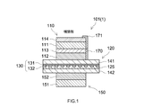
- FIG. 3 is a schematic cross-sectional view showing a main part of an in-cell type liquid crystal display device according to one embodiment.
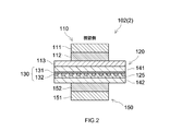
- FIG. 11 is a schematic cross-sectional view showing a main part of an in-cell type liquid crystal display device according to another embodiment. It is a schematic cross-sectional view which shows the main part of the in-cell type liquid crystal display device which concerns on another embodiment.
- FIG. 11 is a schematic cross-sectional view showing a main part of an in-cell type liquid crystal display device according to another embodiment. It is a schematic cross-sectional view which shows the main part of the in-cell type liquid crystal display device which concerns on another embodiment.
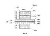
- FIG. 11 is a schematic cross-sectional view showing a main part of an in-cell type liquid crystal display device according to another embodiment.
- FIG. 11 is a schematic cross-sectional view showing a main part of an in-cell type liquid crystal display device according to another embodiment.
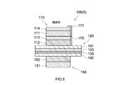
- FIG. 3 is a schematic cross-sectional view showing a main part of a semi-in-cell type liquid crystal display device according to one embodiment.
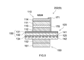
- FIG. 3 is a schematic cross-sectional view showing a main part of an on-cell type liquid crystal display device according to one embodiment. It is explanatory drawing which shows typically the measuring method of the difference of the electric current value of a touch panel at the time of arrange
- 6 is a graph showing a correlation between ⁇ C (Cooked Data (Max-Min)) when a conductive layer is arranged and the surface resistance value [ ⁇ / ⁇ ] of the conductive layer.
- ⁇ C Cooked Data
- the liquid crystal display device with a built-in touch sensing function disclosed herein includes a liquid crystal layer containing liquid crystal molecules, and a touch sensor unit. Further, in the liquid crystal display device, a conductive layer is arranged on the visual side of the touch sensor unit. Further, the liquid crystal display device may typically have a polarizing film (first polarizing film) arranged on the visual side of the liquid crystal layer and on the visual side of the touch sensor unit. Such a liquid crystal display device may be one in which first and second polarizing films are arranged on both sides of a liquid crystal layer.
- At least a part of the touch sensor unit is disposed between the first polarizing film and the liquid crystal layer, and in some aspects, the touch sensor unit (for example, a detection electrode and a drive electrode forming the touch sensor unit) is It is arranged between the first polarizing film and the liquid crystal layer. In some other aspects, a part of the touch sensor unit (for example, the detection electrode) is arranged between the first polarizing film and the liquid crystal layer.
- Examples of liquid crystal display devices with a built-in touch sensing function include devices that include an in-cell liquid crystal panel as shown in FIGS. 1 to 7.
- the in-cell liquid crystal panel is simply a liquid crystal cell including a liquid crystal layer and two transparent substrates sandwiching the liquid crystal layer, in the liquid crystal cell (that is, inside the two transparent substrates). It has a configuration including a touch sensing electrode unit related to the touch sensing function.
- a complete in-cell liquid crystal panel is one in which both the detection electrode and the drive electrode related to the touch sensing function are arranged in the liquid crystal cell.
- FIGS. 1 to 7 are schematic cross-sectional views showing a configuration example of a main part (in-cell type liquid crystal panel) of the liquid crystal display device 1 with a built-in touch sensing function.
- the in-cell type liquid crystal panel 101 shown in FIG. 1 includes a liquid crystal cell (in-cell type liquid crystal cell) 120 and a first polarizing film 111 arranged on the visual side of the liquid crystal cell 120.
- the liquid crystal cell 120 includes a liquid crystal layer 125 containing liquid crystal molecules, and a first transparent substrate 141 and a second transparent substrate 142 arranged so as to sandwich the liquid crystal layer 125.
- the liquid crystal cell 120 includes a touch sensing electrode unit 130 as a touch sensor unit between the first transparent substrate 141 and the second transparent substrate 142.
- the touch sensing electrode unit 130 has a detection electrode 131 and a drive electrode 132.
- the detection electrode is a touch detection (reception) electrode and functions as a capacitance sensor.
- the detection electrode is also called a touch sensor electrode.
- the detection electrodes 131 and the drive electrodes 132 are independently formed in stripes in the X axis direction and the Y axis direction of the plane, Both form a pattern that intersects at right angles to each other.
- the pattern that the touch sensor electrode 130 can form is not limited to this, and the detection electrode 131 and the drive electrode 132 can be formed to have various patterns as described below.
- the first adhesive layer 112, the conductive layer 113, and the first polarizing film 111 are provided in this order from the first transparent substrate 141 toward the viewing side. Specifically, they are laminated.
- the first pressure-sensitive adhesive layer 112, the conductive layer 113, and the first polarizing film 111 are attached to the outer surface of the first transparent substrate 141 on the visible side in the form of the polarizing film with a conductive layer 110. It is attached.
- the conductive layer 113 is provided on one surface of the first polarizing film 111, and the first polarizing layer 113 is placed on one surface of the conductive layer 113 (the surface opposite to the first polarizing film 111 side). It has a structure in which the pressure-sensitive adhesive layer 112 is arranged.
- the first pressure-sensitive adhesive layer 112 is arranged and fixed on the outer surface of the first transparent substrate 141 without a conductive layer.
- the first polarizing film 111 is arranged on the viewing side of the liquid crystal layer 125 so that the transmission axes (or absorption axes) of the polarizers thereof are orthogonal to each other.
- the surface treatment layer 114 is arranged on the back surface side of the first polarizing film 111.
- the second polarizing film 151 is arranged on the opposite side to the viewing side.
- the second polarizing film 151 is attached to the outer surface of the second transparent substrate 142 of the liquid crystal cell 120 via the second adhesive layer 152.
- the second polarizing film 151 is arranged on the back surface side of the liquid crystal layer 125 so that the transmission axis (or absorption axis) of the polarizer is orthogonal to each other.
- the second pressure-sensitive adhesive layer 152 and the second polarizing film 151 are attached to the outer surface of the second transparent substrate 141 in the form of the conductive layer-attached polarizing film 150.
- the polarizing film with a conductive layer 150 has a configuration in which the second adhesive layer 152 is disposed on one surface of the second polarizing film 151.
- a conductive structure 170 made of a conductive material is provided on the side surfaces of the conductive layer 113 and the first adhesive layer 112.
- the conductive structure 170 may be provided on the entire side surface (end surface) of the conductive layer 113 and the first pressure-sensitive adhesive layer 112, or may be provided on a part of the side surface.
- the conductive structure 170 When the conductive structure 170 is provided in a part, in order to secure the conductivity on the side surface, approximately 1% or more, preferably approximately 3% or more of the total area of the side surface of the conductive layer 113 and the first pressure-sensitive adhesive layer 112,
- the conductive structure 170 can be provided at an area ratio of preferably about 10% or more, more preferably about 50% or more.
- the conductive structure 171 is also provided on the side surfaces of the first polarizing film 111 and the surface treatment layer 114.
- the liquid crystal display device 2 with a built-in touch sensing function shown in FIG. 2 is a modified example of the structure shown in FIG. 1, and the layer structure on the viewing side of the liquid crystal cell 120 is different from the structure shown in FIG. Specifically, in the in-cell type liquid crystal panel 102, the conductive layer 113, the first adhesive layer 112, and the first polarizing film 111 are provided on the viewing side of the liquid crystal cell 120 from the first transparent substrate 141 toward the viewing side. The point that they have in order (specifically, that they are laminated) is different from the configuration example of FIG.
- the conductive layer 113 is formed on substantially the entire outer surface of the first transparent substrate 141, and the first pressure-sensitive adhesive layer 112 and the first polarizing film 111 are polarizing films with a conductive layer.
- the polarizing film 110 with a conductive layer has a configuration in which the first pressure-sensitive adhesive layer 112 is arranged on one surface of the first polarizing film 111. Note that, in FIG. 2, the surface treatment layer 114 and the conductive structures 170 and 171 on the back side of the first polarizing film 111 are omitted for convenience of description.
- the first pressure-sensitive adhesive layer 112, the first polarizing film 111, and the conductive layer 113 are attached to the outer surface on the visible side of the first transparent substrate 141 in the form of a polarizing film 110 with a conductive layer. It is attached.
- the first pressure-sensitive adhesive layer 112 is arranged on one surface of the first polarizing film 111, and the other surface of the first polarizing film 111 (opposite side of the surface on which the first pressure-sensitive adhesive layer 112 is formed). The surface is provided with the conductive layer 113.
- the conductive layer 113 may be formed on the back surface of the first polarizing film 111 after laminating the first polarizing film 111 on the visible side of the liquid crystal cell 120. Also in FIG. 3, for convenience of explanation, the surface treatment layer 114 on the back surface side of the first polarizing film 111 and the conductive structures 170 and 171 are omitted.
- the liquid crystal display device 4 with a built-in touch sensing function shown in FIG. 4 is a modified example of the configuration shown in FIG. 1, and in the in-cell type liquid crystal panel 104, the touch sensing electrode portion 130 as a touch sensor portion has a liquid crystal layer 125 and a second portion.
- the structure is different from that shown in FIG. 1 in that it is arranged between the transparent substrate 142 and the transparent substrate 142. That is, the touch sensing electrode unit 130 including the detection electrode 131 and the drive electrode 132 is arranged on the backlight side (back side) with respect to the liquid crystal layer 125.
- the liquid crystal display device 5 with a built-in touch sensing function shown in FIG. 5 is also a modified example of the structure shown in FIG.
- the touch sensing electrode portion 130 in which the detection electrode and the drive electrode are integrally formed is used.
- the point is different from the configuration shown in FIG.
- the liquid crystal display device 6 with a built-in touch sensing function shown in FIG. 6 is a combination of the configurations of FIGS. 4 and 5, and in the in-cell liquid crystal panel 106, a touch sensing electrode portion in which a detection electrode and a drive electrode are integrally formed.
- the configuration differs from that shown in FIG. 1 in that the 130 is used and that the touch sensing electrode unit 130 as the touch sensor unit is arranged on the backlight side (back side) of the liquid crystal layer 125.
- the detection electrode 131 and the drive electrode 132 of the touch sensing electrode part 130 as a touch sensor part are separated on both sides of the liquid crystal layer 125. It is different from the configuration shown in FIG. Specifically, in the in-cell type liquid crystal panel 107, the detection electrode 131 is arranged between the liquid crystal layer 125 and the first transparent substrate 141, and the drive electrode 132 is located between the liquid crystal layer 125 and the second transparent substrate 142. It is located in. Since the other configurations of the modified examples shown in FIGS. 2 to 7 are basically the same as those of the in-cell type liquid crystal panel shown in FIG. 1, overlapping description will be omitted.
- the in-cell type liquid crystal panel has a touch sensing electrode portion inside the liquid crystal cell, not outside the liquid crystal cell.
- an electrode such as an ITO layer (usually, a surface resistance value of 1 ⁇ 10 13 ⁇ / ⁇ or less) is not provided on the outer surface of the first transparent substrate of the liquid crystal cell.
- the semi-in-cell type liquid crystal panel has a liquid crystal cell including a liquid crystal layer and two transparent substrates sandwiching the liquid crystal layer, and a detection electrode and a drive constituting a touch sensing electrode portion related to a touch sensing function. Only one of the electrodes is arranged inside the liquid crystal cell, and the other of the electrodes is arranged outside the liquid crystal cell (typically on the outer surface of the transparent substrate).
- the detection electrode 131 forming the touch sensing electrode unit 130 is provided on the outer surface of the first transparent substrate 141, and the drive electrode 132 forming the touch sensing electrode unit 130 is arranged in the liquid crystal cell 120. ing.
- the drive electrode 132 is arranged between the liquid crystal layer 125 and the second transparent substrate 142.
- the semi-incell type liquid crystal panel 201 has a first polarizing film 111, a conductive layer 113, a first adhesive layer 112, a detection electrode 131, a first transparent substrate 141, a liquid crystal layer 125, a driving electrode 132, and a second transparent.
- the substrate 142 has a laminated structure arranged in this order.
- a surface treatment layer 114 is provided further on the viewing side of the first polarizing film 111. Further, the second pressure-sensitive adhesive layer 152 and the second polarizing film 151 are arranged in this order on the outside of the second transparent substrate 142. In the liquid crystal panel 201, the detection electrode 131 of the touch sensing electrode portion 130 is arranged outside the first transparent substrate 141 and is in contact with the adhesive layer 112.
- the liquid crystal display device with a built-in touch sensing function disclosed herein is a device including an on-cell liquid crystal panel.
- the on-cell type liquid crystal panel has a liquid crystal cell including a liquid crystal layer and two transparent substrates sandwiching the liquid crystal layer, and a touch sensor function is provided on an outer surface of the transparent substrate of the liquid crystal cell.
- the drive electrode 132 is arranged on the outer surface of the first transparent substrate 141 of the liquid crystal cell 120, and the detection electrode 131 is arranged on the drive electrode 132.
- the on-cell type liquid crystal panel 202 includes a first polarizing film 111, a conductive layer 113, a first adhesive layer 112, a detection electrode 131, a drive electrode 132, a first transparent substrate 141, a liquid crystal layer 125, and a drive electrode 134 from the viewer side.
- the second transparent substrate 142 has a laminated structure arranged in this order. Further, a surface treatment layer 114 is provided further on the viewing side of the first polarizing film 111.
- the second pressure-sensitive adhesive layer 152 and the second polarizing film 151 are arranged in this order on the outer side of the second transparent substrate 142.
- the detection electrode 131 of the touch sensing electrode unit 130 is arranged outside the first transparent substrate 141 and is in contact with the first adhesive layer 112.
- a drive electrode 134 is arranged in the liquid crystal cell 120. The drive electrode 134 is arranged between the liquid crystal layer 125 and the second transparent substrate 142.
- the detection electrode is arranged closer to the first transparent substrate side (viewing side) than the drive electrode.
- the configuration of the panel is not limited to this, and the drive electrodes can be arranged on the first transparent substrate side (viewing side) with respect to the detection electrodes.
- the laminated structure on the viewing side of the liquid crystal cell has the first polarizing film, the conductive layer, and the first adhesive layer arranged in this order from the viewing side.
- these structures are formed into a laminated structure in which the first polarizing film 111, the first adhesive layer 112, and the conductive layer 113 are arranged in this order from the visual side. You may change it.
- the laminated structure on the viewing side of the liquid crystal cell of the liquid crystal display device with a built-in touch sensing function shown in FIGS. 4 to 9 is arranged from the viewing side to the conductive layer 113, the first polarizing film 111, and the first polarizing film 111. You may change into the laminated structure which 1 adhesive layer 112 was arrange
- the detection electrodes are arranged outside the liquid crystal cell (specifically, outside the first transparent substrate), and the drive electrodes are arranged inside the liquid crystal cell (specifically, Although it is arranged between the first transparent substrate and the second transparent substrate), the present invention is not limited to this, and the technique disclosed here is that the detection electrode is arranged in the liquid crystal cell and the drive electrode is the liquid crystal. It can be applied to a semi-in-cell type liquid crystal panel arranged outside the cell.
- a polarizing film with an adhesive layer substantially composed of a second adhesive layer and a second polarizing film was used on the back surface side of the liquid crystal cell, which is disclosed here.
- the technique is not limited to this, and it is also possible to use the polarizing film with a conductive layer as used in the configuration example of FIG. 1 on the back side of the liquid crystal panel.
- the polarizing film with a conductive layer disclosed here can be arrange
- the polarizing film that can be arranged on the side opposite to the viewing side the same polarizing film as that arranged on the viewing side may be used, or a different polarizing film may be used.
- a known optical film with a pressure-sensitive adhesive layer may be arranged on the back side of the liquid crystal cell.
- the pressure-sensitive adhesive layer arranged on the back side of the liquid crystal panel the pressure-sensitive adhesive layer disclosed here or a known or commonly used pressure-sensitive adhesive layer can be used depending on the application and purpose.
- the pressure-sensitive adhesive layer may be the same as or different from the pressure-sensitive adhesive layer disposed on the viewer side.
- the thickness of the pressure-sensitive adhesive layer is not particularly limited, and is preferably about 1 to 100 ⁇ m, It is preferably about 2 to 50 ⁇ m, more preferably about 2 to 40 ⁇ m, and further preferably about 5 to 35 ⁇ m.
- a polarizing film and a conductive layer are formed on the visible side and the back side of the liquid crystal cell of the liquid crystal display device having a built-in touch sensing function.
- An easy-adhesion layer can be provided between them, and various easy-adhesion treatments such as corona treatment and plasma treatment can be performed.
- a liquid crystal display device with a touch sensing function is manufactured using a liquid crystal panel (preferably an in-cell type liquid crystal panel) having the configuration described above.
- a liquid crystal panel preferably an in-cell type liquid crystal panel
- various members that can be used in the liquid crystal display device such as using a backlight or a reflector for the lighting system, can be used by a known or conventional method.
- the liquid crystal display device may have a configuration in which a touch panel is provided outside the polarizing film (for example, a configuration in which the touch panel is provided outside the liquid crystal panel of the IPS system or the like).
- the polarizing films disclosed herein are also referred to as polarizing plates, and are usually a polarizing element and at least one surface of the polarizing element (the same applies hereinafter). It may include a transparent protective film arranged on both sides).
- the polarizer is not particularly limited, and for example, a hydrophilic polymer film in which a dichroic substance such as iodine or a dichroic dye is adsorbed and uniaxially stretched is used.
- hydrophilic polymer film examples include polyvinyl alcohol (PVA) film, partially formalized PVA film, ethylene/vinyl acetate copolymer partially saponified film and the like.
- PVA polyvinyl alcohol
- polarizer a polyene-based alignment film such as a dehydrated product of PVA or a dehydrochlorinated product of polyvinyl chloride can also be used.
- a polarizer made of a PVA-based film and a dichroic substance such as iodine is preferable.
- the thickness of the polarizer is not particularly limited and is generally about 80 ⁇ m or less. Further, from the viewpoint of thinning, a thin polarizer having a thickness of about 10 ⁇ m or less (preferably about 1 to 7 ⁇ m) can be used. The thin polarizer has less thickness unevenness and excellent visibility, and has less dimensional change, and thus has excellent durability. The use of a thin polarizer leads to a thin polarizing film.
- thermoplastic resin having excellent transparency, mechanical strength, thermal stability, moisture blocking property, isotropic property, etc.
- a thermoplastic resin having excellent transparency, mechanical strength, thermal stability, moisture blocking property, isotropic property, etc.
- thermoplastic resin include cellulose resins such as triacetyl cellulose (TAC), polyester resins, polyether sulfone resins, polysulfone resins, polycarbonate resins, polyamide resins, polyimide resins, polyolefin resins, (meth)acrylics.
- TAC triacetyl cellulose
- polyester resins such as triacetyl cellulose (TAC)
- polyether sulfone resins such as polyether sulfone resins, polysulfone resins, polycarbonate resins, polyamide resins, polyimide resins, polyolefin resins, (meth)acrylics.
- TAC triacetyl cellulose
- polyester resins such as triacetyl cellulose (TAC)
- a transparent protective film made of a thermoplastic resin such as TAC is arranged on one surface of the polarizer, and a cycloolefin resin (typically norbornene resin) or ( A configuration in which a transparent protective film made of a (meth)acrylic resin is arranged can be adopted.
- a transparent protective film made of a thermoplastic resin such as TAC is arranged on one surface of the polarizer, and a (meth)acrylic-based, urethane-based, acrylic-based acrylic resin is used on the other surface as a transparent protective film.
- a urethane-based, epoxy-based, silicone-based, or other thermosetting resin or an ultraviolet curable resin can be used.
- These transparent protective films can be laminated on the polarizer via an adhesive such as PVA.
- the transparent protective film may contain one or more kinds of any appropriate additive depending on the purpose.
- the adhesive used for laminating the polarizer and the transparent protective film is not particularly limited as long as it is optically transparent, and various types of water-based, solvent-based, hot-melt-based, radical-curable and cation-curable types are used. be able to. Of these, water-based adhesives or radical curable adhesives are preferable.
- a surface treatment layer may be provided on the back surface of the polarizing film.
- the surface treatment layer can be provided on the above-mentioned transparent protective film used for the polarizing film, or can be separately provided on the polarizing film as a separate body from the transparent protective film.
- a preferable example of the surface treatment layer is a hard coat layer.
- a material for forming the hard coat layer for example, a thermoplastic resin or a material that is cured by heat or radiation can be used.
- the material used include a radiation curable resin such as a thermosetting resin, an ultraviolet curable resin, and an electron beam curable resin.
- the ultraviolet curable resin is suitable.
- the ultraviolet curable resin is excellent in processability because the cured resin layer can be efficiently formed by the curing treatment by ultraviolet irradiation.
- the curable resin one type or two or more types of polyester type, acrylic type, urethane type, amide type, silicone type, epoxy type, melamine type and the like can be used, and these include monomers, oligomers, polymers and the like. It can be in the form of inclusion.
- a radiation-curable resin typically an ultraviolet-curable resin is particularly preferable because it does not require heat (which may cause damage to the substrate) and has an excellent processing speed.
- the surface treatment layer include an antiglare treatment layer and an antireflection layer for the purpose of improving visibility.
- An antiglare layer or an antireflection layer may be provided on the hard coat layer.
- the constituent material of the antiglare layer is not particularly limited, and for example, a radiation curable resin, a thermosetting resin, a thermoplastic resin or the like can be used.
- As the antireflection layer titanium oxide, zirconium oxide, silicon oxide, magnesium fluoride and the like can be used.
- the antireflection layer may have a multi-layered structure including a plurality of layers.
- Other examples of the surface treatment layer include a sticking prevention layer and the like.
- the surface treatment layer can be provided with a conductive agent to impart conductivity.
- a conductive agent a conductive agent or a conductive component described below can be used without particular limitation. Therefore, the surface treatment layer can be the conductive layer disclosed herein.
- the surface treatment layer and the conductive layer are provided on the back surface of the polarizing film, the arrangement thereof is not particularly limited, and the surface treatment layer may be arranged between the polarizing film and the conductive layer.
- a conductive layer may be provided between the layers.
- the thickness of the polarizing film disclosed herein is not particularly limited, and is, for example, about 1 ⁇ m or more, usually about 10 ⁇ m or more, and about 20 ⁇ m. The above is appropriate.
- the thickness of the polarizing film is preferably about 30 ⁇ m or more, more preferably about 50 ⁇ m or more, and further preferably about 70 ⁇ m or more from the viewpoint of protection and the like.
- the upper limit of the polarizing film is not particularly limited and is, for example, about 1 mm or less, usually about 500 ⁇ m or less, and about 300 ⁇ m or less is suitable. From the viewpoint of optical characteristics and thickness reduction, the thickness is preferably about 150 ⁇ m or less, more preferably about 120 ⁇ m or less, and further preferably about 100 ⁇ m or less.
- the conductive layer disclosed here is a layer that is arranged on the visual side of the touch sensor unit to increase the conductivity on the visual side of the liquid crystal display device and prevent the occurrence of electrostatic unevenness.
- the conductive layer may be formed from a conductive composition containing various conductive agents such as organic or inorganic conductive substances.
- the pressure-sensitive adhesive layer is arranged on the conductive layer, it may function as an anchor layer that enhances the adhesion between the pressure-sensitive adhesive layer and the polarizing film.
- Organic conductive substances that can be contained in the conductive composition (and therefore also in the conductive layer; the same shall apply hereinafter unless otherwise specified) include quaternary ammonium salts, pyridinium salts, primary amino groups, secondary amino groups, and first.
- Cationic conductive agent having a cationic functional group such as 3 amino group Anionic conductive agent having an anionic functional group such as sulfonate, sulfate ester salt, phosphonate salt, phosphate ester salt; Alkylbetaine and its derivative , Imidazoline and its derivatives, alanine and its derivatives and other amphoteric ionic conductive agents; aminoalcohol and its derivatives, glycerin and its derivatives, polyethylene glycol and its derivatives and other nonionic conductive agents; the above cationic, anionic and amphoteric ions.
- anionic functional group such as sulfonate, sulfate ester salt, phosphonate salt, phosphate ester salt
- Alkylbetaine and its derivative Imidazoline and its derivatives, alanine and its derivatives and other amphoteric ionic conductive agents
- An ion conductive polymer obtained by polymerizing or copolymerizing a monomer having a type ion conductive group for example, a quaternary ammonium salt group.
- Such conductive agents may be used alone or in combination of two or more.
- Examples of the inorganic conductive material that can be contained in the conductive layer include tin oxide, antimony oxide, indium oxide, cadmium oxide, titanium oxide, zinc oxide, indium, tin, antimony, gold, silver, copper, aluminum, nickel and chromium. , Titanium, iron, cobalt, copper iodide, ITO (indium oxide/tin oxide), ATO (antimony oxide/tin oxide) and the like.
- ITO indium oxide/tin oxide
- ATO antimony oxide/tin oxide
- a conductive polymer is used as the conductive agent.
- a conductive layer excellent in optical properties, appearance and antistatic effect can be preferably obtained.
- the moist heat conductive stability improving effect by the technique disclosed herein tends to be preferably exhibited in the conductive layer containing the conductive polymer.
- the conductive polymer include polymers such as polyaniline, polythiophene, polypyrrole, polyquinoxaline, polyethyleneimine, and polyallylamine. Such conductive polymers may be used alone or in combination of two or more.
- Suitable examples of the conductive polymer include polythiophene (thiophene-based polymer) and polyaniline (aniline-based polymer).
- polythiophene means a polymer of unsubstituted or substituted thiophene.
- substituted thiophene polymer in the technology disclosed herein is poly(3,4-ethylenedioxythiophene).
- the conductive polymer those which are soluble in organic solvents, water-soluble, and water-dispersible can be used without particular limitation.
- the conductive polymer is used to form a conductive layer in the form of an aqueous solution or an aqueous dispersion.
- the coating liquid composed of the conductive composition can be in the form of an aqueous liquid (an aqueous solution or an aqueous dispersion liquid which may contain water and another solvent), the risk of alteration of the polarizing film due to the organic solvent can be reduced.
- Conductive polymers such as polyaniline and polythiophene are preferably used because they tend to be in the form of aqueous solutions or aqueous dispersions.
- an aqueous polythiophene solution is used to prepare the conductive composition.
- the aqueous solution or the aqueous dispersion may contain an aqueous solvent in addition to water.
- aqueous solvent for example, methanol, ethanol, n-propanol, isopropanol, n-butanol, isobutanol, sec-butanol, tert-butanol, n-amyl alcohol, isoamyl alcohol, sec-amyl alcohol, tert-amyl alcohol, 1-ethyl-1.
- One or two or more alcohols such as propanol, 2-methyl-1-butanol, n-hexanol, and cyclohexanol can be used in the form of a mixed solvent with water (aqueous solvent).
- the aqueous solution or aqueous dispersion of the above-mentioned conductive polymer is, for example, a conductive polymer having a hydrophilic functional group (which can be synthesized by a method such as copolymerizing a monomer having a hydrophilic functional group in the molecule) in water. It can be prepared by dissolving or dispersing.
- hydrophilic functional group examples include sulfo group, amino group, amide group, imino group, hydroxyl group, mercapto group, hydrazino group, carboxy group, quaternary ammonium group, sulfuric acid ester group (—O—SO 3 H), phosphorus An acid ester group (for example, —O—PO (OH) 2 ) and the like are exemplified.
- Such hydrophilic functional group may form a salt.
- a polyanion is used as a dopant (specifically, a thiophene-based polymer dopant) in the preparation of the conductive composition.
- the conductive layer may include polyanions.
- the polyanion one or more of polycarboxylic acids such as polyacrylic acid and polysulfonic acids such as polystyrene sulfonate (PSS) can be used.
- PSS polystyrene sulfonate
- an aqueous polythiophene solution containing PSS (which may be a form in which PSS is added as a dopant to polythiophene) is used.
- Such an aqueous solution may contain polythiophene: PSS in a weight ratio of 1: 1 to 1:10.
- the total content of polythiophene and PSS in the above aqueous solution can be, for example, about 1 to 5% by weight.
- Examples of commercial products of the above polythiophene aqueous solution include the product name “Denatron” manufactured by Nagase Chemtech and the product name “Clevios” manufactured by Heraeus. Further, as a commercial product of the polyaniline sulfonic acid aqueous solution, a product name “aqua-PASS” manufactured by Mitsubishi Rayon Co., Ltd. is exemplified.
- the content of the conductive agent (preferably the conductive polymer) in the conductive composition is appropriately about 0.005% by weight or more, and preferably about 0.01% by weight or more, from the viewpoint of antistatic.
- the upper limit of the content of the conductive agent (preferably the conductive polymer) in the conductive composition is, for example, about 5% by weight or less, preferably about 3% by weight or less, more preferably about 1% by weight or less. More preferably, it is about 0.7% by weight or less.
- the content of the conductive agent (preferably the conductive polymer) is appropriately about 1% by weight or more, and preferably about 3% by weight, from the viewpoint of antistatic.
- the upper limit of the content of the conductive agent (preferably the conductive polymer) in the conductive layer is preferably about 90% by weight or less.
- the conductive layer may contain a conductive component other than the conductive polymer.
- a conductive component include those exemplified as the above-mentioned organic or inorganic conductive substance (other than the conductive polymer) and the conductive component contained in the pressure-sensitive adhesive layer described later. These can be used alone or in combination of two or more.
- the content of the conductive component other than the conductive polymer in the conductive layer can be set within a range that does not impair the effects of the invention.
- the content thereof is usually about 5% by weight or less in the conductive layer, and it is appropriate that the content is about 3% by weight or less (for example, about 1% by weight or less, typically 0.3% by weight or less). ..
- the technique disclosed herein can be preferably carried out in a manner in which the conductive layer substantially does not contain a conductive component other than the conductive polymer.
- the conductive layer disclosed herein may typically be formed from a conductive composition comprising a high boiling point compound having a boiling point of 180 ° C. or higher.
- the conductive layer formed using the high boiling point compound exhibits improved wet heat conductive stability.
- the liquid crystal display device constructed with the conductive layer can maintain stable touch sensor sensitivity while preventing the occurrence of static electricity unevenness even when exposed to a moist heat environment.
- the high-boiling compounds can be used alone or in combination of two or more.
- the high boiling point compound may not remain due to volatilization when the conductive layer is formed, but the formed conductive layer preferably satisfies the moist heat surface resistance change ratio and the moist heat surface resistance reduction rate, and the moist heat conductivity change ratio FHT is preferable. Can be satisfied.
- the high boiling point compound is a compound having a boiling point of 180° C. or higher, and is a solid or liquid at room temperature (23° C.). As the high boiling point compound that is solid at room temperature, it is preferable to use a compound that is easily dissolved in the solvent (for example, water) of the conductive composition described later.
- Such a high-boiling compound may have a solubility in, for example, 100 mL of a solvent (eg, water) at room temperature of about 1 g or more (typically about 3 g or more, for example, about 10 g or more, further about 20 g or more).
- a solvent eg, water
- the high boiling point compound is preferably a compound which is liquid at a temperature of 20 to 50° C. (and thus has a melting point of 20° C. or less).
- Such compounds are also referred to as high boiling point solvents.
- solvent refers to a liquid medium contained in the conductive composition.
- solvent is a concept that includes the solvent and the dispersion medium.
- the conductive layer has a thin thickness (for example, a thickness of less than 1 ⁇ m), and thus the solvent in the composition Quickly volatilizes and dries.
- the arrangement (which may be the orientation) in the conductive layer of the conductive agent (preferably the conductive polymer) also included in the composition is affected by this drying process.
- the high boiling point compound appropriately controls the volatilization behavior of the solvent in the drying process during the formation of the conductive layer, and as a result, improves the placement of the conductive agent in the conductive layer.
- a high-boiling compound having a boiling point higher than a predetermined value is less likely to change the placement of the conductive agent in the conductive layer due to external factors such as environmental changes in the drying process. It is thought that it is also stable.
- the present inventors have used TOF/MS (time-of-flight mass spectrometer) to prepare a mixed solvent of water and diethylene glycol (boiling point: about 244° C.), water and N-methylpyrrolidone (boiling point: about 204° C.).
- TOF/MS time-of-flight mass spectrometer
- volatilization behavior due to the use of the high boiling point compound contributes to the stable maintenance of the arrangement of the conductive agent, and brings stable conductivity even when exposed to a humid heat environment.
- This action is particularly exerted in a mode in which a thiophene-based polymer or aniline-based polymer that conducts electrons by the action of ⁇ - ⁇ stacking is used as a conductive agent (more preferably, a thiophene-based polymer, for example, a thiophene-based polymer and a dopant such as PSS). It is considered to be particularly meaningful.
- the techniques disclosed herein are not limited to the above considerations.
- the high boiling point compound contained in the conductive composition disclosed herein is also referred to as a conductive stabilizer due to its wet heat conductive stabilizing effect.
- the above-mentioned conductive stabilizer when exposed to a moist heat environment (for example, a temperature of 50° C. or higher and a relative humidity of 80% or higher, typically a temperature of 85° C. and 85% RH) for a predetermined time (for example, 24 hours), As an agent that suppresses changes in the conductivity of the conductive layer (which can be evaluated from the surface resistance value, etc.) as compared with the case where it is not used, that is, as an agent that contributes to stabilizing the conductivity of the conductive layer in the above environment. Can be defined.
- the boiling point of the high boiling point compound contained in the conductive composition is preferably about 200 ° C. or higher, more preferably about 210 ° C. or higher, still more preferably about 220 ° C. or higher from the viewpoint of wet-heat conductive stability. Particularly preferably, it is about 230°C or higher (for example, about 240°C or higher).
- the upper limit of the boiling point of the high boiling point compound is appropriately set in consideration of the film forming property of the conductive layer, the drying efficiency, etc., and is not limited to a specific range.
- the boiling point of the high boiling point compound is usually about 400° C. or lower, and about 320° C.
- adhesion with a layer adjacent to the conductive layer eg, adhesive layer, first polarizing film, first transparent substrate
- it is preferably about 300 ° C. or lower (for example, about 290 ° C. or lower), more preferably about 280 ° C. or lower, still more preferably about 260 ° C. or lower, and particularly preferably about 250 ° C. or lower.
- high boiling point compound examples include lactam compounds such as N-methylpyrrolidone (which may be lactam solvents); ethylene glycol, propylene glycol, trimethylene glycol, butanediols (1,3-butanediol, 1,1).
- lactam compounds such as N-methylpyrrolidone (which may be lactam solvents); ethylene glycol, propylene glycol, trimethylene glycol, butanediols (1,3-butanediol, 1,1).
- glycol compounds such as neopentyl glycol, catechol (may be glycol solvents) ); glycol ether compounds such as diethylene glycol, triethylene glycol, tripropylene glycol, diethylene glycol monomethyl ether, and diethylene glycol monoethyl ether (may be glycol ether solvents); thioglycol compounds such as ⁇ -thiodiglycol ( It can be a thioglycol solvent.); Glycerin; Sugar alcohol compounds such as mannitol, sorbitol, xylitol; Aromatic alcohol compounds such as 2-phenoxyethanol; N-methylformamide, acetamide, N-ethylacetamide, benzamide and the like.
- An amide compound (which may be an amide solvent); an amine compound such as pyrazole (typically a cyclic amine); a sulfoxide compound such as dimethylsulfoxide (which may be a sulfoxide solvent); Those having a boiling point of 180 ° C. or higher can be used without particular limitation. These can be used alone or in combination of two or more. Of these, glycol compounds, glycol ether compounds, and glycerin having a boiling point of 180 ° C. or higher are preferable, and glycol ether compounds having a boiling point of 180 ° C. or higher (typically diethylene glycol and triethylene glycol) are more preferable.
- a compound having a hydroxyl group is preferably used as the high boiling point compound. It is considered that the high boiling point compound having a hydroxyl group is easily compatible with a solvent (typically an aqueous solvent), and when added to an aqueous solvent, for example, can take a good volatile behavior that brings about improvement in wet heat conductivity stability.
- the high boiling point compound contains 2 or more hydroxyl groups, for example 3 or more. Further, for example, those containing an ether structure can be preferably used.
- the content of the high boiling point compound in the conductive composition disclosed herein is appropriately set so as to achieve the target wet heat conductive stability, and thus the wet heat durability of the liquid crystal display device, and is not limited to a specific range.
- the content of the high boiling point compound in the conductive composition is preferably about 0.1% by weight or more, preferably about 0.5% by weight or more, from the viewpoint of obtaining the effect of improving the moist heat conductivity stability. It is preferably about 1% by weight or more, more preferably about 2% by weight or more, and may be about 5% by weight or more (for example, about 8% by weight or more).
- the upper limit of the content of the high boiling point compound in the conductive composition can be, for example, about 50% by weight or less, and about 30% by weight or less (for example, about 25% by weight or less) is suitable for the conductive layer.
- an adjacent layer for example, an adhesive layer, a first polarizing film, a first transparent substrate
- it is preferably about 15% by weight or less, more preferably about 10% by weight or less, still more preferably about 7% by weight.
- % Or less particularly preferably about 5% by weight or less (typically 4% by weight or less).
- the conductive composition for forming the conductive layer typically contains a solvent or a dispersion medium (for convenience, hereinafter collectively referred to as "solvent").
- solvent is not particularly limited, and a solvent capable of stably dissolving or dispersing the conductive layer forming component can be preferably used.
- a solvent can be an organic solvent, water, or a mixed solvent thereof.
- organic solvent examples include esters such as ethyl acetate; ketones such as methyl ethyl ketone, acetone and cyclohexanone; cyclic ethers such as tetrahydrofuran (THF) and dioxane; aliphatic or alicyclic compounds such as n-hexane and cyclohexane.
- esters such as ethyl acetate
- ketones such as methyl ethyl ketone, acetone and cyclohexanone
- cyclic ethers such as tetrahydrofuran (THF) and dioxane
- aliphatic or alicyclic compounds such as n-hexane and cyclohexane.
- Hydrocarbons aromatic hydrocarbons such as toluene and xylene; aliphatic or alicyclic alcohols such as methanol, ethanol, n-propanol, isopropanol and cyclohexanol; alkylene glycol monoalkyl ethers (eg, ethylene glycol monomethyl ethers) , Ethylene glycol monoethyl ether) and other glycol ethers; one or more selected from the above can be used.
- the solvent is a liquid at room temperature and has a boiling point of less than 180°C.
- the solvent is an aqueous solvent.
- the aqueous solvent means water or a mixed solvent containing water as a main component (for example, a mixed solvent of water and a lower alcohol such as methanol or ethanol).
- an aqueous solvent is preferably used. This is preferable from the viewpoint of preventing deterioration of the polarizing film, for example, in the embodiment in which the conductive layer is arranged adjacent to the first polarizing film.
- the ratio of water to the aqueous solvent is appropriately about 30% by weight or more, preferably about 50% by weight or more (typically more than 50% by weight), may be about 70% by weight or more, and is about 80% by weight. The above may be used (for example, about 90 to 100% by weight).
- the conductive layer comprises a binder.
- the film-forming property of the conductive layer is improved, and the adhesion to a layer adjacent to the conductive layer (for example, an adhesive layer, a first polarizing film, a first transparent substrate) is improved.
- the binder is not particularly limited, and includes oxazoline group-containing polymers, urethane-based polymers, acrylic-based polymers, polyester-based polymers, polyether-based polymers, cellulose-based polymers, vinyl alcohol-based polymers, epoxy group-containing polymers, and vinylpyrrolidone-based polymers.
- styrene polymers polyethylene glycol, pentaerythritol and the like may be used. Suitable examples include oxazoline group-containing polymers and urethane-based polymers (typically polyurethane).
- an oxazoline group-containing polymer is used as the binder.
- the oxazoline group-containing polymer may be used alone or in combination of two or more. Oxazoline group-containing polymers that are soluble or dispersible in water are preferred.
- the oxazoline group may be any of a 2-oxazoline group, a 3-oxazoline group, and a 4-oxazoline group, and for example, a group having a 2-oxazoline group can be preferably used.
- oxazoline group-containing polymer for example, a polymer having a (meth) acrylic skeleton or a styrene skeleton in the main chain and having an oxazoline group in the side chain of the main chain can be used.
- the oxazoline group-containing polymer according to some preferred embodiments may be an oxazoline group-containing (meth)acrylic polymer that includes a main chain composed of a (meth)acrylic skeleton and has an oxazoline group in a side chain of the main chain.
- the molecular weight of the oxazoline group-containing polymer can be appropriately set based on the purpose, required characteristics and the like.
- the upper limit of the molecular weight of the oxazoline group-containing polymer is appropriately about 100 ⁇ 10 4 or less, preferably about 50 ⁇ 10 4 or less, and more preferably about 10 ⁇ 10 4 or less, from the viewpoint of coatability. , still more preferably about 5 ⁇ 10 4 or less.
- the above-mentioned molecular weight is the number average molecular weight (Mn) in terms of standard polystyrene obtained by GPC (gel permeation chromatography).
- a urethane polymer is used as the binder.
- the use of the urethane polymer tends to improve the adhesiveness with the layer adjacent to the conductive layer (for example, the pressure-sensitive adhesive layer, the first polarizing film, the first transparent substrate).
- urethane-based polymers include polyurethanes such as ether-based polyurethanes, ester-based polyurethanes and carbonate-based polyurethanes; urethane (meth)acrylates and acryl-urethane copolymers in which alkyl (meth)acrylates are copolymerized.
- the urethane polymer may be used alone or in combination of two or more. In some embodiments, it is preferable to use the oxazoline group-containing polymer and the urethane-based polymer in combination as the binder.
- the content of the binder in the conductive layer is not particularly limited, and for example, it is suitable that it is about 3% by weight or more. From the viewpoint of adhesion and the like, the content of the binder is preferably about 10% by weight or more, more preferably about 30% by weight or more, further preferably about 50% by weight or more, particularly preferably about 60% by weight or more. It may be about 70% by weight or more (for example, about 80% by weight or more).
- the upper limit of the binder content is usually about 99% by weight or less, and about 95% by weight or less is appropriate in consideration of the action of other components such as a conductive polymer, for example, about 90% by weight or less ( For example, about 80% by weight or less).
- Additives can be added to the conductive layer as needed.
- the additive include a leveling agent, an antifoaming agent, a thickener, an antioxidant and the like.
- the ratio of these additives is usually about 50% by weight or less in the conductive layer, and it is appropriate to make it about 30% by weight or less (for example, about 10% by weight or less), and about 3% by weight or less (for example, 1% by weight). It may be less than%).
- the conductive layer is preferably prepared by a method including applying to the polarizing film a liquid conductive composition in which the conductive agent or the high boiling point compound, and the additives used as necessary are dispersed or dissolved in a suitable solvent. Can be formed.
- a method of applying the above-mentioned conductive composition to one surface of a polarizing film, drying it, and performing a curing treatment (heat treatment, ultraviolet treatment, etc.) as necessary can be preferably adopted.
- the conductive composition is subjected to a roll coating method, a bar coating method, a dip coating method, a spin coating method, a casting method, a die coating method, or a gravure coating method.
- Spray coating method, spray printing method, screen printing method, inkjet printing method, offset printing method, etc. are applied to the surface of the first transparent substrate, and if necessary, dried and cured to form a conductive layer. can do.
- the solid content concentration (NV) of the conductive composition can be, for example, 5% by weight or less (typically 0.05 to 5% by weight), and is usually 3% by weight or less (typically 0%).
- the NV of the conductive composition is preferably 0.05 to 0.50 wt% (eg 0.10 to 0.30 wt%). By using such a low NV conductive composition, a more uniform conductive layer can be formed.
- the surface resistance value of the conductive layer is preferably about 1 ⁇ 10 12 ⁇ / ⁇ or less.
- the lower limit of the surface resistance value is preferably about 1 ⁇ 10 6 ⁇ / ⁇ or more.
- the range of the surface resistance value of the conductive layer may differ depending on whether or not the first pressure-sensitive adhesive layer is conductive, the type of liquid crystal cell, the use of portable electronic devices, the use of vehicles, and the like.
- the surface resistance value when applied to an in-cell liquid crystal cell for a portable electronic device, is preferably about 1 ⁇ 10 8 ⁇ / ⁇ to 1 ⁇ 10 10 ⁇ / ⁇ , from the viewpoint of antistatic. Therefore, it is more preferable that it is approximately 1 ⁇ 10 8 ⁇ / ⁇ to 1 ⁇ 10 9 ⁇ / ⁇ .
- the surface resistance value is preferably about 1 ⁇ 10 10 ⁇ / ⁇ to 1 ⁇ 10 12 ⁇ / ⁇ .
- the surface resistance value is preferably about 1 ⁇ 10 9 ⁇ / ⁇ to 1 ⁇ 10 12 ⁇ / ⁇ .
- the surface resistance value of the conductive layer is measured by the method (initial surface resistance value) described in Examples below.
- the conductive layer disclosed herein has, in some embodiments, the surface resistance value S [ ⁇ / ⁇ ] of the conductive layer after a heat and humidity test performed at a temperature of 85° C., a relative humidity of 85%, and a condition of 24 hours. It is characterized in that the ratio with respect to the surface resistance value P [ ⁇ / ⁇ ] of the conductive layer before the wet heat test (wet heat surface resistance change ratio S/P) satisfies the condition: 0.05 ⁇ S/P ⁇ 10. Can be.
- the conductive layer satisfying the moist heat surface resistance change ratio S / P exhibits improved moist heat conductive stability, and can exhibit good touch sensor sensitivity stability even when exposed to a moist heat environment.
- the wet heat surface resistance change ratio S/P is preferably about 0.1 or more, more preferably about 0.5 or more, and further preferably about 0.8 or more (for example, about 1 or more).
- the above S/P is preferably about 3 or less, more preferably about 1.5 or less, further preferably about 1.2 or less, and particularly preferably 1.1 or less.
- the wet heat surface resistance change ratio S/P is measured by the method described in Examples below.
- the liquid crystal display device with a built-in touch sensing function disclosed in the present specification includes a mode in which the wet heat surface resistance change ratio S/P is not limited. It is not limited to those having the above characteristics.
- the conductive layer may have a wet-heat surface resistance reduction rate suppressed to a predetermined value or less.
- the conductive layer may have a moist heat surface resistance reduction rate of 95% or less, which is obtained from the formula: (1-S / P) ⁇ 100 ;.
- S is the surface resistance value [ ⁇ / ⁇ ] of the conductive layer after the wet heat test performed under the conditions of temperature 85° C., relative humidity 85% and 24 hours
- P is the conductive layer before the wet heat test.
- the surface resistance value P [ ⁇ / ⁇ ], and S and P are measured by the method described in Examples described later.
- the conductive layer satisfying the moist heat surface resistance reduction rate can well suppress the decrease in the surface resistance value when exposed to a moist heat environment.
- the wet heat surface resistance reduction rate is preferably about 90% or less, more preferably about 50% or less, further preferably about 20% or less, and particularly preferably about 0% or less. Since the technique disclosed herein may relate to suppressing the decrease in surface resistance when exposed to a moist heat environment, the increase in the surface resistance value after the moist heat test is not particularly limited, but for example, the formula: (S / P).
- the moist heat surface resistance increase rate obtained from -1) ⁇ 100; is appropriately about 200% or less, may be less than 150%, and may be less than 130% (for example, 120% or less).
- S and P in the above formula are synonymous with S and P of the above-mentioned wet heat surface resistance reduction rate, respectively.
- F HT moist heat conductivity change ratio
- Conductive layer disclosed herein is characterized in that moist heat conductive variation ratio is expressed by the following equation (1)
- F HT Hygro- thermal factor
- F HT ⁇ C(B)/ ⁇ C(A)
- ⁇ C(B) is the current of the touch panel that flows when the conductive layer after the heat and humidity test performed under the conditions of the temperature of 85° C., the relative humidity of 85% and the 24 hours is placed on the touch panel for evaluation.
- ⁇ C (A) is the difference between the touch panel current value and the touch panel base current value that flow when the conductive layer before the wet heat test is arranged on the evaluation touch panel. ..
- a conductive layer that satisfies this property maintains stable conductivity even when exposed to a moist heat environment, while maintaining stable touch sensor sensitivity while preventing the occurrence of static electricity unevenness. It is possible to prevent malfunction.
- the FHT is preferably about 1.7 or less, more preferably about 1.5 or less, still more preferably about 1.3 or less, and particularly preferably about 1.1 or less (for example, 1.0). Below).
- the technique disclosed herein may relate to suppressing a decrease in surface resistance (increase in conductivity) when exposed to a moist heat environment
- the decrease in conductivity that is, a decrease in FHT
- the FHT is usually about 0.1 or more (for example, about 0.3 or more), about 0.5 or more is appropriate, preferably about 0.6 or more, and more preferably about 0.7.
- the above is more preferably about 0.8 or more, and particularly preferably about 0.9 or more (typically 0.95 or more, for example, 0.99 or more).
- the FHT is measured by the method described in Examples described later.
- the touch sensing function-equipped liquid crystal display device disclosed herein encompasses the unrestricted mode of the above wet heat conductive variation ratio F HT, in such embodiments, the touch sensing function-equipped liquid crystal display device described above It is not limited to those having characteristics.
- the thickness of the conductive layer in the technique disclosed herein can be appropriately set according to required characteristics such as antistatic property and adhesion.
- the thickness of the conductive layer is usually about 10 nm or more, and it is suitable that the thickness exceeds 10 nm.
- the thickness of the conductive layer is preferably 12 nm or more, more preferably 14 nm or more, still more preferably 15 nm or more, and particularly preferably 20 nm or more (typically 25 nm or more). , For example, 30 nm or more). Further, it is appropriate that the thickness of the conductive layer is about 500 nm or less.
- the thickness of the conductive layer is preferably about 100 nm or less, more preferably about 70 nm or less.
- the effect of using the high boiling point compound disclosed herein effect of improving wet and heat conductive stability
- the liquid crystal display device with a built-in touch sensing function disclosed herein includes a pressure-sensitive adhesive layer (including first and second pressure-sensitive adhesive layers, for the purpose of fixing the first polarizing film to the liquid crystal cell and the like.
- the pressure-sensitive adhesive constituting the pressure-sensitive adhesive layer is, for example, one selected from various pressure-sensitive adhesives such as acrylic, rubber, urethane, silicone, vinylalkyl ether, vinylpyrrolidone, acrylamide, and cellulose. It may be an adhesive layer composed of two or more kinds.
- the polymer constituting the pressure-sensitive adhesive layer may be an acrylic polymer, a rubber polymer, a urethane polymer, a silicone polymer, a vinyl alkyl ether polymer, a vinyl pyrrolidone polymer, an acrylamide polymer, a cellulosic polymer or the like.
- acrylic adhesives are preferable from the viewpoints of transparency, appropriate wettability, adhesive properties such as cohesiveness and adhesiveness, weather resistance, heat resistance and the like.
- the techniques disclosed herein will be described in more detail by taking the configuration in which the pressure-sensitive adhesive layer is an acrylic pressure-sensitive adhesive layer as a main example, but the intention is to limit the pressure-sensitive adhesive layer to one made of an acrylic pressure-sensitive adhesive. is not.
- the acrylic pressure-sensitive adhesive used in some preferred embodiments means an acrylic polymer as a base polymer (a main component among polymer components contained in the pressure-sensitive adhesive, that is, a component contained in an amount of more than 50% by weight).
- the "acrylic polymer” means a monomer having at least one (meth)acryloyl group in one molecule (hereinafter, this may be referred to as "acrylic monomer”) as a main constituent monomer component (monomer). Of 50% by weight or more of the total amount of the monomers constituting the acrylic polymer).
- (meth) acryloyl group has a meaning that comprehensively refers to an acryloyl group and a methacryloyl group.
- (meth)acrylate is meant to mean acrylate and methacrylate inclusively.
- R 2 is 1 to 18 carbon atoms (hereinafter sometimes representing such number range of carbon atoms and C 1-18.)
- a chain alkyl An alkyl(meth)acrylate which is a group (meaning to include a linear alkyl group and a branched alkyl group) is preferable, and an alkyl(meth)acrylate having a C 1-14 chain alkyl group is more preferable.
- chain alkyl group of C 1-14 examples include methyl group, ethyl group, propyl group, isopropyl group, n-butyl group, isobutyl group, s-butyl group, t-butyl group, n-pentyl group, and the like.
- Examples of the alicyclic alkyl group that can be selected as R 2 include a cyclohexyl group and an isobornyl group.
- the total amount of monomers used in the synthesis of the acrylic polymer is approximately 50% by weight or more, more preferably approximately 60% by weight or more, for example, approximately 70% by weight.
- % Or more is a chain (meth) acrylate in which R 2 in the above formula (1) is C 1-18 (more preferably C 1-14 , still more preferably C 4-10 ). For example, it is occupied by one or more selected from n-butyl acrylate (BA) and 2-ethylhexyl acrylate (2EHA) or both).
- An acrylic polymer obtained from such a monomer composition is preferable because a pressure-sensitive adhesive exhibiting adhesive properties suitable for use in liquid crystal display devices can be easily formed.
- the ratio of the chain alkyl (meth) acrylate of C 1-18 (for example, C 1-14 , preferably C 4-10 ) to the total amount of the above-mentioned monomers can be determined by introducing the functional group a or adjusting the phase difference. From the viewpoint of adjusting the refractive index, it is suitable to be about 95% by weight or less, preferably about 90% by weight or less, more preferably 85% by weight or less (for example, 80% by weight or less).
- (meth) acrylate having an aromatic ring structure as a monomer used for synthesizing an acrylic polymer.
- the aromatic ring structure of the (meth) acrylate having an aromatic ring structure include a benzene ring, a naphthalene ring, a thiophene ring, a pyridine ring, a pyrrole ring, and a furan ring.
- (meth)acrylate having a benzene ring or a naphthalene ring is preferable.
- various aryl (meth)acrylates, arylalkyl (meth)acrylates, aryloxyalkyl (meth)acrylates and the like can be used.
- (meth)acrylate having an aromatic ring structure examples include, for example, phenyl(meth)acrylate, o-phenylphenol(meth)acrylate, phenoxy(meth)acrylate, phenoxyethyl(meth)acrylate, phenoxypropyl(meth).
- biphenyl (meth)acrylate it is also possible to use those having a biphenyl ring such as biphenyl (meth)acrylate. These can be used alone or in combination of two or more. Among them, phenoxyethyl (meth)acrylate and benzyl (meth)acrylate are more preferable.
- the (meth)acrylate having an aromatic ring structure is suitable to be about 5% by weight or more of the total amount of monomers used for the synthesis of the acrylic polymer, and the effect of the (meth)acrylate having an aromatic ring structure ( From the viewpoint of satisfactorily exhibiting (improvement of durability, improvement of unevenness of liquid crystal display, etc.), it is preferably about 10% by weight or more, more preferably about 15% by weight or more (for example, about 20% by weight or more).
- the upper limit of the amount of the (meth)acrylate having an aromatic ring structure is appropriately about 30% by weight or less, and preferably about 30% by weight or less, more preferably less than about 30% by weight in consideration of the adhesive properties and the anchoring property of the adhesive layer. It is preferably less than about 25% by weight (for example, less than 22% by weight).
- the acrylic polymer in the technology disclosed herein those obtained by copolymerizing a functional group-containing monomer can be preferably used.
- the functional group-containing monomer include a carboxy group-containing monomer, an acid anhydride group-containing monomer, and a hydroxyl group-containing monomer. These may be used alone or in combination of two or more.
- the functional group-containing monomer can serve as a cross-linking point in the pressure-sensitive adhesive layer, and can improve the cohesive force and heat resistance of the pressure-sensitive adhesive. In addition, the adhesion between the conductive layer and the pressure-sensitive adhesive layer can be improved.
- Tg glass transition temperature
- hydroxyl group-containing monomer 2-hydroxyethyl (meth)acrylate, 2-hydroxypropyl (meth)acrylate, 3-hydroxypropyl (meth)acrylate, 2-hydroxybutyl (meth)acrylate, 4-hydroxybutyl (meth)acrylate , 2-Hydroxyhexyl (meth) acrylate, 6-hydroxyhexyl (meth) acrylate, 8-hydroxyoctyl (meth) acrylate, 10-hydroxydecyl (meth) acrylate, 12-hydroxylauryl (meth) acrylate, (4) Hydroxyalkyl (meth)acrylates such as -hydroxymethylcyclohexyl)methyl (meth)acrylate; alkylene glycol (meth)acrylates such as polyethylene glycol mono (meth)acrylate and polypropylene glycol mono (meth)acrylate; vinyl alcohol, Unsaturated alcohols such as allyl alcohol, 2-hydroxyethyl vinyl ether, 4-hydroxybutyl vinyl ether
- the functional group-containing monomer other than the above may be copolymerized with the acrylic polymer in the technology disclosed herein.
- a monomer can be used, for example, for the purpose of adjusting Tg of an acrylic polymer, adjusting the adhesive performance, and the like.
- the monomer capable of improving the cohesive force and heat resistance of the pressure-sensitive adhesive include a sulfonic acid group-containing monomer, a phosphoric acid group-containing monomer, and a cyano group-containing monomer.
- an amide group-containing monomer capable of introducing a functional group that can serve as a cross-linking point into an acrylic polymer or contributing to improvement of adhesion with an adherend such as glass
- an amide group-containing monomer an amino group-containing monomer, an imide group-containing monomer , Epoxy group-containing monomer, monomer having a nitrogen atom-containing ring, keto group-containing monomer, isocyanate group-containing monomer, alkoxysilyl group-containing monomer and the like.
- an amide group-containing monomer, an amino group-containing monomer, and a monomer having a nitrogen atom-containing ring as exemplified below are preferably used.
- Amide group-containing monomers For example, (meth) acrylamide, N, N-dimethyl (meth) acrylamide, N-butyl (meth) acrylamide, N-methylol (meth) acrylamide, N-methylolpropane (meth) acrylamide, N- Methoxymethyl (meth)acrylamide, N-butoxymethyl (meth)acrylamide.
- Amino group-containing monomer For example, aminoethyl (meth) acrylate, N, N-dimethylaminoethyl (meth) acrylate, N, N-dimethylaminopropyl (meth) acrylate, t-butylaminoethyl (meth) acrylate.
- Monomers having a nitrogen atom-containing ring for example, N-vinyl-2-pyrrolidone, N-methylvinylpyrrolidone, N-vinylpyridine, N-vinylpiperidone, N-vinylpyrimidine, N-vinylpiperazine, N-vinylpyrazin, N-vinyl. Pyrrole, N-vinylimidazole, N-vinyloxazole, N-vinylmorpholin, N-vinylcaprolactam, N- (meth) acryloylmorpholine, N- (meth) acryloylpyrrolidone.
- the monomers having a nitrogen atom-containing ring for example, N-vinyl-2-pyrrolidone, N-methylvinylpyrrolidone, N-vinylcaprolactum, N- (meth) acryloylmorpholin, N- (meth) acryloylpyrrolidone, etc. Needless to say, there are also amide group-containing monomers. The same applies to the relationship between the monomer having a nitrogen atom-containing ring and the amino group-containing monomer.
- the content of the functional group-containing monomer is not particularly limited, and is usually about 40% by weight or less, and about 30% by weight, of the total amount of the monomers used for synthesizing the base polymer (typically an acrylic polymer).
- the following is appropriate, and from the viewpoint of adhesive properties and the like, it is preferably about 20% by weight or less, more preferably about 15% by weight or less, still more preferably 10% by weight or less (for example, 5% by weight or less).
- the lower limit of the content of the functional group-containing monomer in the total amount of monomers used for the synthesis of the base polymer is usually about 0.001% by weight or more, and about 0.01% by weight or more is suitable. From the viewpoint of preferably exerting the effect of the monomer copolymerization, it is preferably about 0.1% by weight or more, more preferably about 0.5% by weight or more, still more preferably about 1% by weight or more.
- At least one (preferably both) of a carboxy group-containing monomer and a hydroxyl group-containing monomer is used as a monomer component of a base polymer (typically an acrylic polymer).
- a base polymer typically an acrylic polymer.
- the amount of the carboxy group-containing monomer in the total amount of the monomers used in the synthesis of the base polymer is usually from the viewpoint of cohesiveness of the pressure-sensitive adhesive, anchorability, etc.
- Approximately 0.001% by weight or more, approximately 0.01% by weight or more is suitable, preferably approximately 0.1% by weight or more, more preferably approximately 0.2% by weight or more, for example, 1% by weight or more. Or may be 3% by weight or more.
- the upper limit of the amount of the carboxy group-containing monomer used is appropriately set so as to obtain the desired adhesive properties, and about 10% by weight or less of the total amount of the monomers used in the synthesis of the base polymer is suitable, preferably about 8. By weight% or less, more preferably about 6% by weight or less, for example, about 3% by weight or less, or about 1% by weight or less.
- the amount of the hydroxyl group-containing monomer in the total amount of the monomers used for the synthesis of the base polymer is the cohesiveness of the pressure-sensitive adhesive, the anchoring property, etc. From this viewpoint, it is usually about 0.001% by weight or more, about 0.01% by weight or more is suitable, and preferably about 0.1% by weight or more.
- the upper limit of the amount of the hydroxyl group-containing monomer used is appropriately set so as to obtain the desired adhesive properties, and about 5% by weight or less of the total amount of the monomers used for synthesizing the base polymer is appropriate, preferably about 3% by weight. % Or less, more preferably about 1% by weight or less (for example, about 0.5% by weight or less).
- Vinyl compounds such as cyclohexyl (meth)acrylate, t-butylcyclohexyl (meth)acrylate, cyclopentyl (meth)acrylate, isobornyl (meth)acrylate; ethylene, propylene, isoprene, butadiene, Olefin-based monomers such as isobutylene; Chlorine-containing monomers such as vinyl chloride and vinylidene chloride; alkoxy group-containing monomers such as methoxyethyl (meth) acrylate and ethoxyethyl (meth) acrylate; Vinyl ether-based monomers such as methyl vinyl ether, ethyl vinyl ether and isobutyl vinyl ether.
- non-aromatic ring-containing (meth)acrylates such as cyclohexyl (meth)acrylate, t-butylcyclohexyl (meth)acrylate, cyclopentyl (meth)acrylate
- Monomer can be used alone or in combination of two or more.
- the amount used is not particularly limited and is usually approximately 30% by weight of the total amount of the monomers used in the synthesis of the base polymer (typically an acrylic polymer). It is suitable to be below (for example, 0 to 30% by weight), preferably about 10% by weight or less (for example, about 3% by weight or less).
- the technique disclosed herein can also be carried out in an embodiment in which the monomer component used for the synthesis of the base polymer does not substantially contain the above-mentioned other copolymerizable monomer.
- a copolymerizable monomer that can constitute a base polymer is a polyfunctional monomer.
- the polyfunctional monomer include 1,6-hexanediol di(meth)acrylate, ethylene glycol di(meth)acrylate, pentaerythritol di(meth)acrylate, trimethylolpropane tri(meth)acrylate, dipentaerythritol hexa.
- examples thereof include compounds having two or more (meth) acryloyl groups in one molecule, such as (meth) acrylate and methylenebisacrylamide.
- the polyfunctional monomers may be used alone or in combination of two or more.
- the amount thereof is not particularly limited and is usually about 2% by weight or less (more preferably about 1% by weight or less) of the total amount of the monomers used for the synthesis of the base polymer. It is appropriate to do.
- Examples of such a redox type initiator include a combination of peroxide and ascorbic acid (a combination of hydrogen peroxide solution and ascorbic acid, etc.), a combination of a peroxide and an iron (II) salt (hydrogen peroxide solution). (Combination of iron (II) salt, etc.), combination of persulfate and sodium hydrogen peroxide, etc.
- Such polymerization initiators may be used alone or in combination of two or more.
- the amount of the polymerization initiator used may be a usual amount, for example, about 0.005 to 1 part by weight (typically 0.01 to 1 part by weight) with respect to 100 parts by weight of all the raw material monomers. You can choose from a range.
- the method for obtaining a base polymer (typically an acrylic polymer) having such a monomer composition is not particularly limited, and various polymerization methods such as a solution polymerization method, an emulsion polymerization method, a bulk polymerization method and a suspension polymerization method are used. obtain.
- photopolymerization performed by irradiating light such as UV (typically performed in the presence of a photopolymerization initiator), radiation polymerization performed by irradiating radiation such as ⁇ -ray or ⁇ -ray.
- Active energy ray irradiation polymerization may be adopted.
- the solution polymerization method can be preferably adopted from the viewpoints of transparency and adhesive performance.
- a batch charging method of supplying all the monomer raw materials at once a continuous supply (dropping) method, a divided supply (dropping) method, or the like can be appropriately adopted.
- the polymerization temperature can be appropriately selected depending on the type of monomer and solvent used, the type of polymerization initiator, etc., and may be, for example, about 20 ° C. to 170 ° C. (typically 40 ° C. to 140 ° C.). it can.
- the base polymer to be synthesized may be a random copolymer, a block copolymer, a graft copolymer or the like. From the viewpoint of productivity and the like, a random copolymer is usually preferable.
- aromatic compounds typically aromatic hydrocarbons
- acetic acid esters such as ethyl acetate
- aliphatic or fat such as hexane.
- Cyclic hydrocarbons halogenated alkanes such as 1,2-dichloroethane
- lower alcohols such as isoprop
- Base polymer (acrylic polymer) in the art disclosed herein may suitably be GPC weight average molecular weight in terms of standard polystyrene obtained by (Gel Permeation Chromatography) (Mw) is at approximately 10 ⁇ 10 4 or more From the viewpoint of durability, heat resistance, etc., preferably about 50 ⁇ 10 4 or more, more preferably about 80 ⁇ 10 4 or more, and further preferably about 120 ⁇ 10 4 or more (for example, about 150 ⁇ 10 4 or more). Is. Further, the Mw is suitably about 500 ⁇ 10 4 or less, and from the viewpoint of coatability at the time of forming the pressure-sensitive adhesive layer, preferably about 300 ⁇ 10 4 or less, more preferably about 250 ⁇ 10 4 or less, more preferably about 200 ⁇ 10 4 or less.
- the above Mw can be measured under the following conditions using the trade name "HLC-8120GPC" (manufactured by Tosoh Corporation) as a GPC measuring device.
- GPC measurement conditions Sample concentration: 0.2 wt% (tetrahydrofuran solution) Sample injection volume: 100 ⁇ L Eluent: Tetrahydrofuran (THF) Flow rate (flow rate): 0.8 mL/min Column temperature (measurement temperature): 40°C Column: Made by Tosoh, G7000H XL + GMH XL + GMH XL Column size: Each 7.8 mm ⁇ ⁇ 30 cm Total 90 cm Detector: Differential refractometer (RI) Standard sample: polystyrene
- the technique disclosed herein can be preferably implemented in a mode in which the pressure-sensitive adhesive layer contains a conductive component.
- the antistatic component include ionic compounds.
- a conductive agent that may be contained in the conductive layer may be used. These conductive components may be used alone or in combination of two or more.
- the adhesive layer comprises an ionic compound.
- the ionic compound, as a conductive component preferably improves the conductivity of the pressure-sensitive adhesive layer.
- one or more selected from alkali metal salts and organic cation-anion salts are preferably used. From the viewpoint of anchoring property, an organic cation-anion salt is more preferable.
- Alkali metal salt organic salts and inorganic salts of alkali metals can be used.
- alkali metal ion forming the cation part of the alkali metal salt include lithium, sodium and potassium ions. Among these alkali metal ions, lithium ion is preferable.
- the anion part of the alkali metal salt may be composed of an organic material or an inorganic material.
- the anion portion constituting the organic salt include CH 3 COO ⁇ , CF 3 COO ⁇ , CH 3 SO 3 ⁇ , CF 3 SO 3 ⁇ , (CF 3 SO 2 ) 3 C ⁇ , C 4 F 9 SO 3 -, C 3 F 7 COO - , (CF 3 SO 2) (CF 3 CO) N -, (FSO 2) 2 N -, - O 3 S (CF 2) 3 SO 3 -, PF 6 -, CO 3 2- and the following general formulas (1) to (4): (1) (C n F 2n+1 SO 2 ) 2 N ⁇ (where n is an integer of 1 to 10); (2) CF 2 (C m F 2m SO 2 ) 2 N ⁇ (where m is an integer of 1 to 10); (3) - O 3 S ( CF 2) l SO 3 - ( provided that, l is an integer of 1 to 10); (4) (C
- the anionic portion of the inorganic, Cl -, Br -, I -, AlCl 4 -, Al 2 Cl 7 -, BF 4 -, PF 6 -, ClO 4 -, NO 3 -, AsF 6 -, SbF 6 -, NbF 6 ⁇ , TaF 6 ⁇ , (CN) 2 N ⁇ and the like are used.
- (perfluoroalkylsulfonyl) imides such as (CF 3 SO 2 ) 2 N ⁇ and (C 2 F 5 SO 2 ) 2 N ⁇ are preferable, and are represented by (CF 3 SO 2 ) 2 N ⁇ .
- (Trifluoromethanesulfonyl) imide is particularly preferred.
- organic salt of an alkali metal examples include sodium acetate, sodium alginate, sodium ligninsulfonate, sodium toluenesulfonate, LiCF 3 SO 3 , Li(CF 3 SO 2 ) 2 N, Li(CF 3 SO 2 ) 2 N, Li (C 2 F 5 SO 2) 2 N, Li (C 4 F 9 SO 2) 2 N, Li (CF 3 SO 2) 3 C, KO 3 S (CF 2) 3 SO 3 K, LiO 3 S (CF 2) 3 SO 3 K , and the like.
- LiCF 3 SO 3, Li ( CF 3 SO 2) 2 N, Li (C 2 F 5 SO 2) 2 N, Li (C 4 F 9 SO 2) 2 N, Li (CF 3 SO 2) 3 C and the like are preferable, and fluorine-containing lithium imide salts such as Li(CF 3 SO 2 ) 2 N, Li(C 2 F 5 SO 2 ) 2 N and Li(C 4 F 9 SO 2 ) 2 N are more preferable, and Perfluoroalkylsulfonyl)imide lithium salts are particularly preferred.
- the inorganic salt of the alkali metal include lithium perchlorate and lithium iodide.
- the said alkali metal salt may be used individually by 1 type, and may be used in combination of 2 or more type.
- Organic cation-anion salt used in the technology disclosed herein refers to an organic salt whose cation component is composed of an organic substance, and the anion component may be an organic substance, It may be an inorganic substance.
- the cation component constituting the organic cation-anion salt include pyridinium cation, piperidinium cation, pyrrolidinium cation, cation having a pyrolin skeleton, cation having a pyrrol skeleton, imidazolium cation, and tetrahydropyrimidi.
- Examples thereof include nium cation, dihydropyrimidinium cation, pyrazolium cation, pyrazolinium cation, tetraalkylammonium cation, trialkylsulfonium cation, tetraalkylphosphonium cation and the like.
- anion component of the organic cation-anion salt examples include Cl ⁇ , Br ⁇ , I ⁇ , AlCl 4 ⁇ , Al 2 Cl 7 ⁇ , BF 4 ⁇ , PF 6 ⁇ , ClO 4 ⁇ , NO 3 ⁇ , CH 3 COO -, CF 3 COO -, CH 3 SO 3 -, CF 3 SO 3 -, (CF 3 SO 2) 3 C -, AsF 6 -, SbF 6 -, NbF 6 -, TaF 6 -, (CN) 2 N -, C 4 F 9 SO 3 -, C 3 F 7 COO -, (CF 3 SO 2) (CF 3 CO) N -, (FSO 2) 2 N -, - O 3 S (CF 2) 3 SO 3 - or the following general formulas (1) to (4): (1) (C n F 2n+1 SO 2 ) 2 N ⁇ (where n is an integer of 1 to 10); (2) CF 2 (C m F 2m SO 2
- ionic compound in addition to the above-mentioned alkali metal salt and organic cation-anionic salt, inorganic salts such as ammonium chloride, aluminum chloride, copper chloride, ferric chloride, ferric chloride and ammonium sulfate can also be used. it can.
- inorganic salts such as ammonium chloride, aluminum chloride, copper chloride, ferric chloride, ferric chloride and ammonium sulfate can also be used. it can.
- the ionic compounds disclosed herein also include those generally referred to as ionic surfactants.
- a cationic surfactant having a cationic functional group such as quaternary ammonium salt, phosphonium salt, sulfonium salt, pyridinium salt and amino group; carboxylic acid, sulfonate, sulfate, phosphate, phosphite, etc.
- An anionic surfactant having an anionic functional group a zwitterionic surfactant such as sulfobetaine and its derivatives, alkylbetaine and its derivatives, imidazoline and its derivatives, alkylimidazolium betaine and its derivatives; and the like. ..
- the organic cation-anion salt may be used alone or in combination of two or more.
- the ionic compound examples include an ionic solid and an ionic liquid, and the ionic liquid is preferably used.
- the ionic liquid easily moves in the pressure-sensitive adhesive layer and is easily dispersed uniformly in the layer.
- an ionic liquid is used as the ionic compound, the effects of the techniques disclosed herein tend to be preferably exhibited.
- Ionic liquid refers to molten salt that is liquid at 40°C or lower.
- the ionic liquid can be easily added to, dispersed or dissolved in the pressure-sensitive adhesive in the temperature range in which the liquid is exhibited, as compared with the solid salt. Further, since the ionic liquid has no vapor pressure (nonvolatile), it has a characteristic that it does not disappear over time and the antistatic property is continuously obtained.
- the ionic liquid used in the techniques disclosed herein is preferably a molten salt that is liquid at room temperature (25 ° C.).
- an organic cation-anionic salt ionic liquid of an organic cation-anionic salt that is liquid at 40 ° C.
- organic cation-anionic salt ionic liquid of an organic cation-anionic salt that is liquid at room temperature (25 ° C.) is preferable.
- Organic cation-anion salt ionic liquids are more preferred.
- the content of the ionic compound (preferably organic cation-anion salt) in the pressure-sensitive adhesive layer is not particularly limited, and an appropriate amount capable of imparting predetermined conductivity to the pressure-sensitive adhesive layer may be added.
- the amount of the ionic compound with respect to 100 parts by weight of the base polymer (eg, acrylic polymer) is appropriately about 0.01 parts by weight or more (eg, about 0.05 parts by weight or more), and from the viewpoint of improving conductivity. It is preferably about 0.1 parts by weight or more, more preferably about 0.3 parts by weight or more, still more preferably about 0.5 parts by weight or more, and particularly preferably about 0.7 parts by weight or more.
- the content of the conductive component in the pressure-sensitive adhesive layer is not particularly limited, and an appropriate amount capable of imparting predetermined conductivity to the pressure-sensitive adhesive layer can be added.
- the amount of the conductive component relative to 100 parts by weight of the base polymer is appropriately about 0.01 parts by weight or more, and from the viewpoint of improving conductivity, preferably about 0.1 parts by weight or more, More preferably, it is about 0.5 part by weight or more.
- the upper limit of the amount of the conductive component is about 30 parts by weight or less with respect to 100 parts by weight of the base polymer, and preferably about 10 parts by weight or less in consideration of durability and adhesive properties.
- the pressure-sensitive adhesive layer may optionally contain a conductive component other than the ionic compound in addition to the ionic compound, or may be substantially not contained.
- the technique disclosed herein can be carried out in such a manner that the pressure-sensitive adhesive layer does not substantially contain a conductive component other than an ionic compound.
- the form of the pressure-sensitive adhesive composition used for forming the pressure-sensitive adhesive layer is not particularly limited.
- a pressure-sensitive adhesive composition containing a pressure-sensitive adhesive component in an organic solvent solvent-type pressure-sensitive adhesive composition
- a pressure-sensitive adhesive composition in which a pressure-sensitive adhesive component is dispersed in an aqueous solvent water-dispersed pressure-sensitive adhesive composition, typically Is an aqueous emulsion-type pressure-sensitive adhesive composition
- a solventless pressure-sensitive adhesive composition for example, a pressure-sensitive adhesive composition that is cured by irradiation with active energy rays such as ultraviolet rays and electron beams, hot-melt pressure-sensitive adhesive composition.
- the technique disclosed here can be preferably implemented in an aspect including a pressure-sensitive adhesive layer formed from a solvent-based pressure-sensitive adhesive composition.
- the organic solvent contained in the solvent-type pressure-sensitive adhesive composition may be, for example, a single solvent consisting of any one of toluene, xylene, ethyl acetate, hexane, cyclohexane, methylcyclohexane, heptane and isopropyl alcohol, and any of these. It may be a mixed solvent containing as a main component.
- the pressure-sensitive adhesive composition (preferably a solvent-type pressure-sensitive adhesive composition) used for forming the pressure-sensitive adhesive layer is a base polymer (typically an acrylic polymer) contained in the composition. It is possible to preferably employ those configured so that (1) can be appropriately crosslinked.
- a cross-linking base point is introduced into the base polymer by copolymerizing a monomer having an appropriate functional group (hydroxyl group, carboxy group, etc.) and reacts with the functional group to form a cross-linked structure.
- a method of adding a compound (crosslinking agent) capable of reacting to the base polymer to cause a reaction can be preferably adopted.
- cross-linking agent examples include isocyanate-based cross-linking agents, epoxy-based cross-linking agents, oxazoline-based cross-linking agents, aziridine-based cross-linking agents, melamine-based cross-linking agents, carbodiimide-based cross-linking agents, hydrazine-based cross-linking agents, amine-based cross-linking agents, and imine-based cross-linking agents.
- Agents for example, benzoyl peroxide), metal chelate crosslinking agents (typically polyfunctional metal chelates), metal alkoxide crosslinking agents, metal salt crosslinking agents and the like.
- the cross-linking agents may be used alone or in combination of two or more.
- isocyanate crosslinking agents epoxy crosslinking agents, peroxide crosslinking agents, and metal chelate crosslinking agents are preferable.
- an acrylic polymer is used as the base polymer
- an isocyanate-based cross-linking agent and a peroxide-based cross-linking agent are preferable, and a combination of the isocyanate-based cross-linking agent and the peroxide-based cross-linking agent is more preferable.
- the amount of the cross-linking agent used can be appropriately selected depending on the composition and structure (molecular weight, etc.) of the base polymer (for example, acrylic polymer), the application of the liquid crystal display device, and the like.
- the amount of the cross-linking agent used with respect to 100 parts by weight of the base polymer is appropriately about 0.01 parts by weight or more, and preferably about 0.02 parts by weight or more from the viewpoint of enhancing the cohesive force of the pressure-sensitive adhesive. , And more preferably about 0.03 parts by weight or more (for example, 0.1 parts by weight or more).
- the upper limit of the amount of the cross-linking agent used is usually about 10 parts by weight or less relative to 100 parts by weight of the base polymer, and from the viewpoint of wettability to an adherend, preferably about 5 parts by weight. Hereinafter, it is more preferably about 3 parts by weight or less, and further preferably about 1 part by weight or less.
- various additives can be added to the above-mentioned pressure-sensitive adhesive composition.
- additives include surface lubricants, leveling agents, plasticizers, softeners, fillers, antioxidants, preservatives, light stabilizers, UV absorbers, polymerization inhibitors, cross-linking accelerators, silane couplings.
- agents include agents.
- a known or commonly used tackifier resin or peeling modifier may be blended in the pressure-sensitive adhesive composition using an acrylic polymer as a base polymer.
- an emulsifier or a chain transfer agent also referred to as a molecular weight modifier or a polymerization degree modifier
- the content of the additives as these optional components can be appropriately determined according to the purpose of use.
- the amount of the optional additive used is usually about 5 parts by weight or less with respect to 100 parts by weight of the base polymer, and it is appropriate that the amount is about 3 parts by weight or less (for example, about 1 part by weight or less).
- the pressure-sensitive adhesive layer is formed, for example, by directly applying the pressure-sensitive adhesive composition as described above to the polarizing film, or by applying it on the conductive layer provided on the polarizing film and then drying or curing it (direct method). can do.
- the pressure-sensitive adhesive composition is applied to the surface (release surface) of a release liner and dried or cured to form a pressure-sensitive adhesive layer on the surface, and the pressure-sensitive adhesive layer is attached to a polarizing film, or It may be formed by a method of transferring the pressure-sensitive adhesive layer by bonding it to the surface of the conductive layer provided on the polarizing film (transfer method).
- the pressure-sensitive adhesive composition In applying (typically applying) the pressure-sensitive adhesive composition, various methods such as a roll coating method and a gravure coating method can be appropriately adopted.
- the pressure-sensitive adhesive composition can be dried under heating if necessary.
- ultraviolet rays, laser rays, ⁇ rays, ⁇ rays, ⁇ rays, X rays, electron rays and the like can be appropriately adopted.
- the surface resistance value of the adhesive layer is not particularly limited.
- the pressure-sensitive adhesive layer is configured to have conductivity in addition to the conductive layer, so that higher conductivity can be imparted to the visual side of the liquid crystal display device.
- the surface resistance value of the pressure-sensitive adhesive layer is appropriately about 1 ⁇ 10 12 ⁇ / ⁇ or less from the viewpoint of antistatic properties.
- the lower limit of the surface resistance value is preferably about 1 ⁇ 10 7 ⁇ / ⁇ or more.
- the surface resistance value is preferably about 1 ⁇ 10 10 ⁇ / ⁇ to 1 ⁇ 10 12 ⁇ / ⁇ .
- the surface resistance value is preferably about 1 ⁇ 10 9 ⁇ / ⁇ to 1 ⁇ 10 12 ⁇ / ⁇ .
- the surface resistance value is preferably about 1 ⁇ 10 7 ⁇ / ⁇ to 1 ⁇ 10 12 ⁇ / ⁇ , and from the viewpoint of durability, it is about. It is more preferably 1 ⁇ 10 8 ⁇ / ⁇ to 1 ⁇ 10 10 ⁇ / ⁇ .
- the surface resistance value of the pressure-sensitive adhesive layer is measured by the method described in Examples below.
- the thickness of the pressure-sensitive adhesive layer can be, for example, about 1 ⁇ m or more, and usually about 3 ⁇ m or more is suitable. From the viewpoint of antistatic property, durability, and securing the contact area with the conduction path when the conduction path is provided on the side surface, the thickness of the pressure-sensitive adhesive layer is preferably about 5 ⁇ m or more, more preferably about 7 ⁇ m or more, and further. It is preferably about 10 ⁇ m or more. The above-mentioned thickness can be, for example, about 100 ⁇ m or less, and normally, about 50 ⁇ m or less (for example, about 35 ⁇ m or less) is preferable.
- a liquid crystal layer containing liquid crystal molecules is used as a liquid crystal layer forming a liquid crystal cell.
- the liquid crystal layer is a liquid crystal layer containing homogenically oriented liquid crystal molecules in the absence of an electric field.
- an IPS type liquid crystal layer is preferably used as the liquid crystal layer.
- Other examples of the liquid crystal layer that can be used in the technology disclosed herein include TN type, STN type, ⁇ type, and VA type liquid crystal layers.
- the thickness of the liquid crystal layer is, for example, about 1.5 ⁇ m to 4 ⁇ m.
- the detection electrodes and the drive electrodes (including both integrated) that constitute the touch-sensing electrode section are typically transparent conductive layers (transparent electrodes).
- the material of these electrodes is not particularly limited, and examples thereof include metals such as gold, silver, copper, platinum, palladium, aluminum, nickel, chromium, titanium, iron, cobalt, tin, magnesium and tungsten, and alloys of these metals. One kind or two or more kinds can be used. Further, as the electrode material, one or more kinds of metal oxides of indium, tin, zinc, gallium, antimonide, zirconium and cadmium can be used. Specific examples include metal oxides composed of indium oxide, tin oxide, titanium oxide, cadmium oxide, and mixtures thereof.
- the metal oxide may further contain an oxide of the metal atom exemplified above, if necessary.
- ITO indium oxide
- tin oxide tin oxide containing antimony, and the like
- ITO is particularly preferably used.
- the ITO those containing about 80 to 99% by weight of indium oxide and about 1 to 20% by weight of tin oxide are preferably used.
- a detection electrode as a touch sensing electrode portion, a drive electrode, and an electrode integrally formed with both are usually at least one of a first transparent substrate and a second transparent substrate (typically only one). Is formed as a transparent electrode pattern inside (on the side of the liquid crystal layer in the liquid crystal cell).
- one of the detection electrode and the drive electrode is formed inside one of the first transparent substrate and the second transparent substrate (the liquid crystal layer side in the liquid crystal cell), and The other is formed outside the other of the first transparent substrate and the second transparent substrate.
- the detection electrode, the drive electrode, and the electrode in which both are integrally formed are formed outside the first transparent substrate and the second transparent substrate (outside the liquid crystal cell).
- the electrode pattern can be formed by a conventional method.
- the detection electrode, the drive electrode, and the electrode formed integrally with each other in the touch sensing electrode portion may also have a function as a common electrode for controlling the liquid crystal layer.
- the electrode pattern is usually electrically connected to a lead wire (not shown) formed at the end of the transparent substrate.
- the lead wire is connected to a controller IC (not shown).
- the shape of the electrode pattern is not limited to the one in which the striped wiring is orthogonal as in the above configuration example, and for example, in addition to the striped shape, an arbitrary shape such as a comb shape or a diamond shape, depending on the application, purpose, etc. Can be taken. Therefore, the detection electrode and the drive electrode may have an intersection pattern other than a right angle and various other patterns.
- the height of the electrode pattern may be, for example, approximately 10 nm to 100 nm, and the width may be approximately 0.1 mm to 5 mm.
- the material forming the transparent substrate includes, for example, glass or polymer film. Therefore, the transparent substrate can be a glass substrate or a polymer substrate.
- the glass used for the transparent substrate is not particularly limited, and various glass materials can be used.
- the polymer film include polyethylene terephthalate (PET), polycycloolefin, polycarbonate and the like.
- PET polyethylene terephthalate
- the transparent substrate is mainly formed of a glass plate, its thickness is, for example, about 0.1 mm to 1 mm.
- the transparent substrate is mainly formed of a polymer film, its thickness is, for example, about 10 ⁇ m to 200 ⁇ m.
- the transparent substrate may have an easy adhesion layer or a hard coat layer on its surface.
- Various conductive materials can be used without particular limitation as the material for forming the conductive structure connected to the side surface of the pressure-sensitive adhesive layer and the conductive layer.
- a conductive paste such as a metal paste containing one or more of silver, gold and other metals is preferably used.
- Other examples of the above materials include conductive adhesives.
- the conductive structure may have a linear shape extending from the side surface of the conductive layer or the pressure-sensitive adhesive layer. The same applies to the material having a conductive structure that can be provided on the side surface of the polarizing film or the like, and the shape can be the same as described above.
- a polarizing film or a known or common optical film different from the polarizing film is used depending on the application or purpose. be able to.
- an optical film include a retardation film (also referred to as a retardation plate, including a wavelength plate), an optical compensation film, a brightness enhancement film, a light diffusion film, a reflection film, an anti-transmission film and the like. They can be used alone or in combination of two or more.
- the application of the liquid crystal display device with a built-in touch sensing function (also referred to as a touch panel type liquid crystal display device) disclosed herein is not particularly limited, and can be used for various purposes such as for portable electronic devices and for vehicles.
- the technology disclosed herein may be particularly suitable for a vehicle-mounted touch panel type liquid crystal display device that is easily exposed to a harsh environment and is required to have a wet heat durability higher than a predetermined level.
- a pressure-sensitive adhesive layer used for manufacturing a liquid crystal display device is formed on a release liner, and an applied voltage of 250 V is applied to the surface of the pressure-sensitive adhesive layer in an atmosphere of temperature 23° C. and 50% RH in accordance with JIS K 6911.
- the surface resistance value [ ⁇ / ⁇ ] is measured under the condition that the application time is 10 seconds.
- the resistivity meter a commercially available resistivity meter (for example, trade name "Hiresta UP MCP-HT450 type" manufactured by Mitsubishi Chemical Analytech Co., Ltd.) or an equivalent product thereof can be used.
- Table 1 described later when the resistance value exceeds the upper limit of measurement, it is described as "OVER".
- the polarizing film sample with a conductive layer is set on the cover glass 304 of the touch panel 302 of the evaluation kit 300, and the surface of the pressure-sensitive adhesive layer of the polarizing film sample S with a conductive layer. was attached so as not to cause floating.
- the touch panel 302 is horizontally placed on an insulator (not shown).
- the insulator for example, a plate-shaped resin or a frame-shaped rubber body can be used.
- the software activated on the PC acquires the capacitance data map in the plane of the touch panel 302 through the terminal T and the IC substrate, and the obtained current value of the touch panel and the touch panel base current value without the polarizing film sample S with the conductive layer.
- FIG. 11 is a graph in which the ⁇ C (Cooked Data (Max-Min)) measured above is plotted on the vertical axis and the surface resistance value [ ⁇ / ⁇ ] of the conductive layer is plotted on the horizontal axis. As shown in FIG. 11, since the correlation coefficient R 2 of the regression line between the ⁇ C and the surface resistance value [ ⁇ / ⁇ ] showed a high correlation of 0.9701, the ⁇ C was the same as that of the conductive layer.
- ⁇ C is a value that has been digitally (8-bit) converted by the software, the unit is bit.
- ⁇ C(A), ⁇ C(B) and the wet heat conductivity change ratio F HT described later are bit.
- a plurality of insulating sheets may be superposed on the upper surface (back surface) of the conductive layer-attached polarizing film sample as a weight.
- the conductivity is concerned. Place the layer surface so as to contact the cover glass of the evaluation kit, and then place a plurality of insulating sheets (for example, a touch panel) as a weight on the conductive layer so that the conductive layer and the cover glass do not float.
- ⁇ C (A) The polarizing film with a conductive layer used for manufacturing a liquid crystal display device is set in the evaluation kit 300 by the same method as in (1) above, and from the acquired capacitance data map in the touch panel surface, when the polarizing film with a conductive layer is set.
- the difference ⁇ C (Cooked Data) between the touch panel current value and the touch panel base current value is obtained. This is defined as the difference ⁇ C (A) between the current value of the touch panel and the touch panel base current value that flows when the conductive layer before the moist heat test is arranged on the evaluation touch panel.
- ⁇ C(A) can be measured by directly using the conductive layer instead of the polarizing film with the conductive layer.
- the polarizing film with a conductive layer used for manufacturing a liquid crystal display device is left for 24 hours in a moist heat environment at a temperature of 85 ° C. and 85% RH (wet heat test). Then, about the thing dried at room temperature for 3 hours, it set to the evaluation kit 300 by the method similar to said (1), and from the acquired capacity data map of the touch panel surface, the current of the touch panel at the time of setting the polarizing film with a conductive layer was set. The difference ⁇ C (Cooked Data) between the value and the base current value of the touch panel is obtained.
- ESD electrostatic discharge test
- An in-cell type liquid crystal cell is prepared, the release liner is peeled off from the polarizing film with a conductive layer, and the exposed adhesive surface is bonded to the visible side of the in-cell type liquid crystal cell as shown in FIG.
- a silver paste having a width of 5 mm was applied to the side surface of the polarizing film with a conductive layer attached to the in-cell liquid crystal cell so as to cover all the side surfaces of the hard coat layer, the polarizing film, the conductive layer, and the pressure-sensitive adhesive layer.
- a liquid crystal display panel is obtained by connecting to a ground electrode from the outside. Under the conditions of 23 ° C.
- the liquid crystal display panel was set on the backlight device, and an electrostatic discharge gun (Electro-static Discharge Gun) was fired on the polarizing film surface on the visual side at an applied voltage of 10 kV. Measure the time until the white spot disappears due to electricity (initial evaluation). Further, the same ESD test is also carried out after the liquid crystal display panel is put into a moist heat environment at a temperature of 85 ° C. and 85% RH for 24 hours and then dried at room temperature for 3 hours (evaluation after moist heat). The obtained measurement results are evaluated according to the following criteria. (Evaluation criteria) ⁇ : White unevenness disappears within 3 seconds both in the initial stage and after moist heat. ⁇ : White unevenness disappears within 5 seconds in either the initial stage or after moist heat. ⁇ : Even if it exceeds 5 seconds in both the initial stage and after moist heat. White unevenness does not disappear.
- Preparation of polarizing film Swelling a long roll of a polyvinyl alcohol (PVA)-based resin film (Kuraray Co., Ltd., product name "PE3000”) having a thickness of 30 ⁇ m while uniaxially stretching it by a roll stretching machine so as to be 5.9 times in the longitudinal direction, It was dyed, crosslinked, washed, and finally dried to obtain a polarizer having a thickness of 12 ⁇ m. Specifically, in the swelling treatment, the film was stretched 2.2 times while being treated with pure water at 20 ° C. In the dyeing treatment, the film was stretched 1.4 times while being treated at 30 ° C.
- PVA polyvinyl alcohol
- the weight ratio of iodine to potassium iodide was 1:7.
- the cross-linking treatment a two-step cross-linking treatment was adopted, and in the first-step cross-linking treatment, the film was stretched 1.2 times while being treated in a boric acid / potassium iodide aqueous solution at 40 ° C.
- the boric acid content of this aqueous solution was 5.0%, and the potassium iodide content was 3.0%.
- the film was stretched 1.6 times while being treated in a boric acid / potassium iodide aqueous solution at 65 ° C.
- the boric acid content of this aqueous solution was 4.3%, and the potassium iodide content was 5.0%.
- the cleaning treatment a 20° C. potassium iodide aqueous solution was used.
- the potassium iodide content of the aqueous solution for cleaning treatment was set to 2.6%.
- the drying process was performed at 70° C. for 5 minutes.
- a 32 ⁇ m-thick TAC-HC film having a hard coat (HC) layer on one side of the triacetyl cellulose (TAC) film was bonded to one side of the above-mentioned polarizer using a PVA-based adhesive.
- a 25 ⁇ m-thick acrylic (CAT) film is attached to the other surface of the above polarizer using a PVA adhesive to form a polarizing film having a structure of TAC protective layer/PVA polarizer/CAT protective layer. It was made.
- a hard coat layer is provided as a surface treatment layer on the surface of the polarizing film on the TAC protective layer side.
- Preparation of conductive composition (Preparation example B1) 14.3 parts of a thiophene-based polymer-containing solution (PEDOT / PSS-NH 4 ) and binder solution A (trade name "Superflex 210" manufactured by Daiichi Kogyo Seiyaku Co., Ltd., containing urethane binder, solid content 35%).
- binder solution B manufactured by Nippon Catalyst Co., Ltd., trade name "Epocross WS-700", containing oxazolin group-containing polymer of Mn 20,000, Mw 40,000
- triethylene glycol as a high boiling point compound (boiling point: about 287° C.) and water were mixed to prepare a conductive composition B1 having a solid content concentration of 1.5%.
- thiophene-based polymer-containing liquid an aqueous dispersion containing PEDOT (poly (3,4-ethylenedioxythiophene)) and PSS (poly (styrene sulfonic acid) sodium) (manufactured by Heleus, trade name "CleviosP"
- PEDOT poly (3,4-ethylenedioxythiophene)
- PSS poly (styrene sulfonic acid) sodium
- the product was neutralized with 28% ammonia water manufactured by Tokyo Kasei Kogyo Co., Ltd. to have a solid content of 1%.
- Triethylene glycol was blended to contain 3% in the composition.
- the resulting composition contained 0.14% thiophene-based polymer, 0.36% urethane binder, and 1.0% oxazoline group-containing polymer.
- Preparation Example B2 A conductive composition B2 according to this example was prepared in the same manner as in Preparation Example B1 except that diethylene glycol (boiling point: about 244° C.) was used as the high-boiling compound instead of triethylene glycol.
- Preparation Example B3 A conductive composition B3 according to this example was prepared in the same manner as in Preparation Example B1 except that catechol (boiling point: about 246° C.) was used as the high-boiling compound instead of triethylene glycol.
- Preparation Example B4 A conductive composition B4 according to this example was prepared in the same manner as in Preparation Example B3, except that the amount of the high-boiling compound (catechol) added was changed from 3% to 10% and the amount of water was reduced accordingly.
- the high-boiling compound (catechol) added was changed from 3% to 10% and the amount of water was reduced accordingly.
- a conductive composition B5 according to this example was prepared in the same manner as in Preparation Example B1 except that glycerin (boiling point: about 290° C.) was used instead of triethylene glycol.
- Preparation Example B6 A conductive composition B6 according to this example was prepared in the same manner as in Preparation example B1 except that N-methylpyrrolidone (boiling point: about 204° C.) was used as the high-boiling compound instead of triethylene glycol.
- Preparation Example B7 As the high boiling point compound, 5% of dimethyl sulfoxide (boiling point: about 189 ° C.) was used instead of 3% of triethylene glycol, and the amount of water was reduced by that amount, but the conductivity according to this example was the same as in Preparation Example B1. Composition B7 was prepared.
- Preparation Example B8 A conductive composition B8 according to this example was prepared in the same manner as in Preparation Example B1 except that the high-boiling compound was not used.
- Preparation Example B9 A conductive composition B9 according to this example was prepared in the same manner as in Preparation example B1 except that N,N-dimethylformamide (boiling point: about 153° C.) was used instead of triethylene glycol.
- Preparation Example B10 The conductive composition B10 according to this example was prepared in the same manner as in Preparation Example B1 except that diethylene glycol dimethyl ether (boiling point: about 162 ° C.) was used instead of triethylene glycol.
- Preparation example C2 6 parts of a conductive agent is added to 100 parts of the solid content of the acrylic polymer P1 solution, and an isocyanate-based cross-linking agent (manufactured by Toso Co., Ltd., trade name "Coronate L", trimethylolpropane / tolylene diisocyanate adduct) 0.
- an isocyanate-based cross-linking agent manufactured by Toso Co., Ltd., trade name "Coronate L", trimethylolpropane / tolylene diisocyanate adduct
- Examples 1 to 11 and Comparative Examples 1 to 3 A coating liquid composed of any of the above conductive compositions B1 to B10 is applied to one side of the above polarizing film (the side on which the hard coat layer is not provided) so that the thickness after drying is 50 nm, and at 80 ° C. It was dried for 3 minutes to form a conductive layer.
- a solution of any of the above acrylic pressure-sensitive adhesive compositions C1 to C2 was applied to one side of a polyethylene terephthalate (PET) film (release liner, manufactured by Mitsubishi Chemical Polyester Film Co., Ltd., product number “MRF38”) treated with a silicone-based release agent.
- PET polyethylene terephthalate
- the film was applied so that the thickness of the pressure-sensitive adhesive layer after drying was 23 ⁇ m, and the film was dried at 155 ° C. for 1 minute to form a pressure-sensitive adhesive layer on the surface of the release liner. Then, the pressure-sensitive adhesive layer formed on the release liner was transferred onto the surface of the polarizing film obtained above on the conductive layer side.
- the polarizing film with a conductive layer according to each example was produced.
- These polarizing films with a conductive layer have a structure of polarizing film/conductive layer/adhesive layer, and a hard coat layer is provided on the back side of the polarizing film, and the adhesive surface of the adhesive layer is protected by a release liner. Has been done.
- a liquid crystal display device with a built-in touch sensing function according to each example was produced by connecting a routing wiring (not shown) around the transparent electrode pattern inside the in-cell type liquid crystal cell to a controller IC (not shown).
- the wet heat surface resistance change ratio of the conductive layer was within the range of 0.05 or more and 10 or less.
- the touch sensitivity stability evaluation results were all acceptable levels.
- the wet-heat conductivity change ratio FHT was also 2 or less.
- the wet heat surface resistance change ratio of the conductive layer was in a narrower range, and particularly excellent evaluation results were obtained.
- the moist heat conductivity change ratio FHT is 2 or less, and the moist heat surface resistance change of the conductive layer.
- Liquid crystal display device with a built-in touch sensing function 110 Polarizing film with a conductive layer 111: First polarizing film 112: First adhesive layer 113: Conductive layer 114 : Surface treatment layer 101, 102, 103, 104, 105, 106, 107: In-cell type liquid crystal panel 201: Semi-in-cell type liquid crystal panel 202: On-cell type liquid crystal panel 120: Liquid crystal cell 125: Liquid crystal layer 130: Touch sensing electrode section (touch) Sensor part) 131: detection electrode 132: drive electrode 141: first transparent substrate 142: second transparent substrate 150: polarizing film with adhesive layer 151: second polarizing film 152: second adhesive layer 170: conductive structure 171: conductive structure 300 : Evaluation kit 302: Touch panel 304: Cover glass S: Polarizing film sample with conductive layer
Landscapes
- Physics & Mathematics (AREA)
- Chemical & Material Sciences (AREA)
- Nonlinear Science (AREA)
- General Physics & Mathematics (AREA)
- Engineering & Computer Science (AREA)
- Crystallography & Structural Chemistry (AREA)
- Mathematical Physics (AREA)
- Optics & Photonics (AREA)
- Theoretical Computer Science (AREA)
- General Engineering & Computer Science (AREA)
- Health & Medical Sciences (AREA)
- Chemical Kinetics & Catalysis (AREA)
- Medicinal Chemistry (AREA)
- Polymers & Plastics (AREA)
- Organic Chemistry (AREA)
- Human Computer Interaction (AREA)
- Liquid Crystal (AREA)
- Compositions Of Macromolecular Compounds (AREA)
Abstract
Description
本出願は、2019年3月5日に出願された日本国特許出願2019-039938号に基づく優先権を主張しており、その出願の全内容は本明細書中に参照として組み入れられている。
FHT=ΔC(B)/ΔC(A)・・・・・(1)
(式(1)中、ΔC(B)は、温度85℃、相対湿度85%および24時間の条件で実施される湿熱試験後の導電層を評価用タッチパネル上に配したときに流れるタッチパネルの電流値とタッチパネルベース電流値との差分であり、ΔC(A)は、前記湿熱試験前の導電層を評価用タッチパネル上に配したときに流れるタッチパネルの電流値とタッチパネルベース電流値との差分である。)
なお、以下の図面において、同じ作用を奏する部材・部位には同じ符号を付して説明し、重複する説明は省略または簡略化することがある。また、図面に記載の実施形態は、本発明を明瞭に説明するために模式化されており、実際に提供される製品および部品のサイズや縮尺を正確に表したものではない。
ここに開示されるタッチセンシング機能内蔵液晶表示装置は、液晶分子を含む液晶層と、タッチセンサ部と、を備える。また、上記液晶表示装置において、タッチセンサ部よりも視認側には導電層が配置されている。さらに、上記液晶表示装置は、典型的には、液晶層の視認側であってタッチセンサ部よりも視認側に偏光フィルム(第1偏光フィルム)が配置されたものであり得る。そのような液晶表示装置は、液晶層の両側に第1および第2の偏光フィルムがそれぞれ配置されたものであり得る。タッチセンサ部の少なくとも一部は、第1偏光フィルムと液晶層との間に配置されており、いくつかの態様では、タッチセンサ部(例えばタッチセンサ部を構成する検出電極および駆動電極)は、第1偏光フィルムと液晶層との間に配置されている。他のいくつかの態様では、タッチセンサ部の一部(例えば検出電極)が、第1偏光フィルムと液晶層との間に配置されている。
ここに開示される偏光フィルム(第1および第2の偏光フィルムを包含する。特に断りがない限り以下同じ。)は偏光板ともいい、通常、偏光子と、該偏光子の少なくとも一方の面(好ましくは両面)に配置された透明保護フィルムとを備えるものであり得る。偏光子としては、特に限定されず、例えば、親水性高分子フィルムに、ヨウ素や二色性染料の二色性物質を吸着させて一軸延伸したものが用いられる。親水性高分子フィルムとしては、ポリビニルアルコール(PVA)系フィルム、部分ホルマール化PVA系フィルム、エチレン・酢酸ビニル共重合体系部分ケン化フィルム等が挙げられる。偏光子として、PVAの脱水処理物やポリ塩化ビニルの脱塩酸処理物等のポリエン系配向フィルム等を用いることもできる。なかでも、PVA系フィルムとヨウ素等の二色性物質からなる偏光子が好ましい。
ここに開示される導電層は、タッチセンサ部よりも視認側に配置されて、液晶表示装置の視認側の導電性を高め、静電ムラの発生を防止する層である。導電層は、例えば、有機または無機の導電性物質等の各種導電剤を含む導電性組成物から形成され得る。導電層の上に粘着剤層が配置される態様においては、粘着剤層と偏光フィルムとの密着を高めるアンカー層として機能するものであり得る。
いくつかの好ましい態様では、導電剤として導電性ポリマーを用いる。導電性ポリマーを用いることにより、光学特性、外観、帯電防止効果に優れた導電層が好ましく得られる。また、ここに開示される技術による湿熱導電安定性向上効果は、導電性ポリマーを含む導電層において、好ましく発揮される傾向がある。導電性ポリマーとしては、ポリアニリン、ポリチオフェン、ポリピロール、ポリキノキサリン、ポリエチレンイミン、ポリアリルアミン等のポリマーが挙げられる。このような導電性ポリマーは、1種を単独で使用してもよく、2種以上を組み合わせて使用してもよい。
ここに開示される導電層は、典型的には、沸点が180℃以上である高沸点化合物を含む導電性組成物から形成したものであり得る。上記高沸点化合物を用いて形成した導電層は、改善した湿熱導電安定性を示す。上記導電層を備えて構築された液晶表示装置は、湿熱環境に曝された場合であっても、静電気ムラの発生を防止しつつ、安定したタッチセンサ感度を保持することができる。高沸点化合物は1種を単独でまたは2種以上を組み合わせて用いることができる。高沸点化合物は導電層形成時に揮発により残存しないものであり得るが、形成された導電層は、湿熱表面抵抗変化比や湿熱表面抵抗減少率を好ましく満足し、湿熱導電性変化比FHTを好ましく満足し得る。上記高沸点化合物は、沸点が180℃以上である化合物であり、常温(23℃)で固体または液体である。常温で固体である高沸点化合物は、後述する導電性組成物の溶媒(例えば水)に対して、溶解しやすいものを用いることが好ましい。そのような高沸点化合物は、例えば溶媒(例えば水)100mLへの溶解度が常温で凡そ1g以上(典型的には凡そ3g以上、例えば凡そ10g以上、さらには凡そ20g以上)であり得る。また、導電層形成性の観点から、高沸点化合物は温度20~50℃で液状(したがって融点が20℃以下)の化合物であることが好ましい。そのような化合物は高沸点溶媒ともいう。なお、ここでいう溶媒とは、導電性組成物に含まれる液状媒体をいい、便宜上溶媒というが、溶媒および分散媒を包含する概念である。
いくつかの態様において、導電層はバインダを含む。導電層がバインダを含むことにより、導電層の膜形成性が向上するとともに、導電層に隣接する層(例えば粘着剤層や第1偏光フィルム、第1透明基板)との密着性が向上する。バインダとしては、特に限定されず、オキサゾリン基含有ポリマー、ウレタン系ポリマー、アクリル系ポリマー、ポリエステル系ポリマー、ポリエーテル系ポリマー、セルロース系ポリマー、ビニルアルコール系ポリマー、エポキシ基含有ポリマー、ビニルピロリドン系ポリマー、スチレン系ポリマー、ポリエチレングリコール、ペンタエリスリトール等の1種または2種以上が用いられ得る。好適例としては、オキサゾリン基含有ポリマー、ウレタン系ポリマー(典型的にはポリウレタン)が挙げられる。
上記導電層は、上記導電剤や高沸点化合物、必要に応じて使用される添加剤が適当な溶媒に分散または溶解した液状の導電性組成物を偏光フィルムに付与することを含む手法によって好適に形成され得る。例えば、上記導電性組成物を偏光フィルムの一方の面に塗布して乾燥させ、必要に応じて硬化処理(熱処理、紫外線処理等)を行う手法を好ましく採用し得る。あるいは、第1透明基板の外表面に導電層を形成する態様においては、導電性組成物を、ロールコート法、バーコート法、ディップコーティング法、スピンコーティング法、キャスティング法、ダイコート法、グラビアコート法、スプレーコート法、スプレー印刷法、スクリーン印刷法、インクジェット印刷法、オフセット印刷法等の公知の手段で第1透明基板の表面に付与し、必要に応じて乾燥、硬化させることにより導電層を形成することができる。上記導電性組成物の固形分濃度(NV)は、例えば5重量%以下(典型的には0.05~5重量%)とすることができ、通常は3重量%以下(典型的には0.10~3重量%)とすることが適当である。薄厚の導電層を形成する場合には、上記導電性組成物のNVを例えば0.05~0.50重量%(例えば0.10~0.30重量%)とすることが好ましい。このように低NVの導電性組成物を用いることにより、より均一な導電層が形成され得る。
導電層の表面抵抗値は、帯電防止等の観点から、凡そ1×1012Ω/□以下であることが適当である。表面抵抗値が所定値以下に制限された導電層を液晶パネル(例えばインセル型液晶パネル)用途に適用すると、導電層の導電性に基づき静電気ムラの発生が防止される。また、タッチセンサ感度の観点から、上記表面抵抗値の下限は、凡そ1×106Ω/□以上とすることが好ましい。導電層の表面抵抗値の範囲は、第1粘着剤層が導電性であるか否か、液晶セルの種類、携帯電子機器用途や車載用途等によって異なり得る。例えば、携帯電子機器用のインセル型液晶セルに適用する場合には、上記表面抵抗値は、凡そ1×108Ω/□~1×1010Ω/□であることが好ましく、帯電防止の観点から、凡そ1×108Ω/□~1×109Ω/□であることがより好ましい。車載用のインセル型液晶セルに適用する場合には、凡そ1×106Ω/□~1×109Ω/□であることが好ましく、帯電防止の観点から、凡そ1×107Ω/□~5×108Ω/□であることがより好ましい。また、オンセル型液晶セルに適用する場合には、上記表面抵抗値は、凡そ1×1010Ω/□~1×1012Ω/□であることが好ましい。また、セミインセル型液晶セルに適用する場合には、上記表面抵抗値は、凡そ1×109Ω/□~1×1012Ω/□であることが好ましい。導電層の表面抵抗値は、後述の実施例に記載の方法(初期表面抵抗値)で測定される。
ここに開示される導電層は、いくつかの態様において、温度85℃、相対湿度85%および24時間の条件で実施される湿熱試験後における導電層の表面抵抗値S[Ω/□]と上記湿熱試験前における導電層の表面抵抗値P[Ω/□]との比(湿熱表面抵抗変化比S/P)が、条件:0.05≦S/P≦10;を満足することを特徴とするものであり得る。上記湿熱表面抵抗変化比S/Pを満足する導電層は、改善された湿熱導電安定性を示し、湿熱環境に曝された場合であっても、良好なタッチセンサ感度安定性を発揮し得る。上記湿熱表面抵抗変化比S/Pは、好ましくは凡そ0.1以上、より好ましくは凡そ0.5以上、さらに好ましくは凡そ0.8以上(例えば凡そ1以上)である。また上記S/Pは、好ましくは凡そ3以下、より好ましくは凡そ1.5以下、さらに好ましくは凡そ1.2以下、特に好ましくは1.1以下である。湿熱表面抵抗変化比S/Pは、後述の実施例に記載の方法で測定される。なお、本明細書に開示されるタッチセンシング機能内蔵液晶表示装置は、上記湿熱表面抵抗変化比S/Pの制限のない態様を包含し、そのような態様において、タッチセンシング機能内蔵液晶表示装置は上記特性を有するものに限定されない。
いくつかの態様において、導電層は、湿熱表面抵抗減少率が所定値以下に抑制されたものであり得る。具体的には、導電層は、式:(1-S/P)×100;から求められる湿熱表面抵抗減少率が95%以下であり得る。ここでSは、温度85℃、相対湿度85%および24時間の条件で実施される湿熱試験後における導電層の表面抵抗値[Ω/□]であり、Pは、上記湿熱試験前における導電層の表面抵抗値P[Ω/□]であり、SおよびPは、後述の実施例に記載の方法で測定される。上記湿熱表面抵抗減少率を満足する導電層は、湿熱環境に曝された場合における表面抵抗値の減少をよく抑制するものであり得る。上記湿熱表面抵抗減少率は、好ましくは凡そ90%以下、より好ましくは凡そ50%以下、さらに好ましくは凡そ20%以下、特に好ましくは凡そ0%またはそれ以下である。ここに開示される技術は、湿熱環境に曝した場合における表面抵抗減少抑制に関するものであり得るので、湿熱試験後の表面抵抗値の増大については特に限定されないが、例えば、式:(S/P-1)×100;から求められる湿熱表面抵抗増加率は、凡そ200%以下であることが適当であり、150%未満であってもよく、130%未満(例えば120%以下)であり得る。上式中のSおよびPは上記湿熱表面抵抗減少率のSおよびPとそれぞれ同義である。
ここに開示される導電層は、いくつかの態様において、次式(1)で表される湿熱導電性変化比FHT(Hygro-thermal factor)が2以下であることを特徴とするものであり得る。
FHT=ΔC(B)/ΔC(A)・・・・・(1)
上式(1)中、ΔC(B)は、温度85℃、相対湿度85%および24時間の条件で実施される湿熱試験後の導電層を評価用タッチパネル上に配したときに流れるタッチパネルの電流値とタッチパネルベース電流値との差分であり、ΔC(A)は、前記湿熱試験前の導電層を評価用タッチパネル上に配したときに流れるタッチパネルの電流値とタッチパネルベース電流値との差分である。この特性を満足する導電層は、湿熱環境に曝された場合であっても、安定した導電性を保持し、静電気ムラの発生を防止しつつ、安定したタッチセンサ感度を保持し、タッチセンサの誤作動を防止することができる。そのような観点から、上記FHTは、好ましくは凡そ1.7以下、より好ましくは凡そ1.5以下、さらに好ましくは凡そ1.3以下、特に好ましくは凡そ1.1以下(例えば1.0以下)である。ここに開示される技術は、湿熱環境に曝した場合における表面抵抗減少(導電性上昇)抑制に関するものであり得るので、湿熱試験後の導電性低下(すなわちFHTの減少)については特に限定されないが、上記FHTは、通常は凡そ0.1以上(例えば凡そ0.3以上)であり、凡そ0.5以上が適当であり、好ましくは凡そ0.6以上、より好ましくは凡そ0.7以上、さらに好ましくは凡そ0.8以上、特に好ましくは凡そ0.9以上(典型的には0.95以上、例えば0.99以上)である。上記FHTは、後述の実施例に記載の方法で測定される。なお、本明細書に開示されるタッチセンシング機能内蔵液晶表示装置は、上記湿熱導電性変化比FHTの制限のない態様を包含し、そのような態様において、タッチセンシング機能内蔵液晶表示装置は上記特性を有するものに限定されない。
ここに開示される技術における導電層の厚さは、帯電防止性、密着性等の要求特性に応じて適切に設定され得る。導電層の厚さは、通常は、凡そ10nm以上であり、10nm超とすることが適当である。帯電防止性向上や、均一な厚みを得る観点から、導電層の厚さは、好ましくは12nm以上、より好ましくは14nm以上、さらに好ましくは15nm以上、特に好ましくは20nm以上(典型的には25nm以上、例えば30nm以上)である。また、導電層の厚さは凡そ500nm以下とすることが適当である。導電層の厚さを凡そ500nm以下に抑制することにより、良好な光学特性(全光線透過率等)が得られやすい。そのような観点から、導電層の厚さは、好ましくは凡そ100nm以下、より好ましくは凡そ70nm以下である。薄厚の導電層を備える構成において、ここに開示される高沸点化合物使用の効果(湿熱導電安定性改善効果)は好ましく発揮され得る。
ここに開示されるタッチセンシング機能内蔵液晶表示装置は、第1偏光フィルムの液晶セルへの固定等を目的として、粘着剤層(第1および第2の粘着剤層を包含する。特に断りがない限り以下同じ。)を備えるものであり得る。粘着剤層を構成する粘着剤は、例えば、アクリル系、ゴム系、ウレタン系、シリコーン系、ビニルアルキルエーテル系、ビニルピロリドン系、アクリルアミド系、セルロース系等の各種粘着剤から選択される1種または2種以上を含んで構成された粘着剤層であり得る。したがって、粘着剤層を構成するポリマーは、アクリル系ポリマー、ゴム系ポリマー、ウレタン系ポリマー、シリコーン系ポリマー、ビニルアルキルエーテル系ポリマー、ビニルピロリドン系ポリマー、アクリルアミド系ポリマー、セルロース系ポリマー等であり得る。なかでも、透明性、適度の濡れ性、凝集性や接着性等の粘着特性、耐候性、耐熱性等の観点から、アクリル系粘着剤が好ましい。以下、上記粘着剤層がアクリル系粘着剤層である構成を主な例として、ここに開示される技術をより詳しく説明するが、上記粘着剤層をアクリル系粘着剤からなるものに限定する意図ではない。
いくつかの好ましい態様で採用されるアクリル系粘着剤とは、アクリル系ポリマーをベースポリマー(該粘着剤に含まれるポリマー成分のなかの主成分、すなわち50重量%よりも多く含まれる成分)とする粘着剤をいう。また、「アクリル系ポリマー」とは、1分子中に少なくとも1つの(メタ)アクリロイル基を有するモノマー(以下、これを「アクリル系モノマー」ということがある。)を主構成単量体成分(モノマーの主成分、すなわちアクリル系ポリマーを構成するモノマーの総量のうち50重量%以上を占める成分)とするポリマーを指す。上記「(メタ)アクリロイル基」とは、アクリロイル基およびメタクリロイル基を包括的に指す意味である。同様に、「(メタ)アクリレート」とは、アクリレートおよびメタクリレートを包括的に指す意味である。
上記アクリル系粘着剤のベースポリマーたるアクリル系ポリマーは、典型的には、アルキル(メタ)アクリレートを主構成単量体成分とするポリマーである。上記アルキル(メタ)アクリレートとしては、例えば、下記式(1)で表される化合物を好適に用いることができる。
CH2=C(R1)COOR2 (1)
ここで、上記式(1)中のR1は、水素原子またはメチル基である。R2は、炭素原子数1~20のアルキル基である(鎖状アルキル基および脂環式アルキル基を包含する意味である。)。粘着特性に優れた粘着剤が得られやすいことから、R2が炭素原子数1~18(以下、このような炭素原子数の範囲をC1-18と表わすことがある。)の鎖状アルキル基(直鎖状アルキル基および分岐状アルキル基を包含する意味である。)であるアルキル(メタ)アクリレートが好ましく、C1-14の鎖状アルキル基を有するアルキル(メタ)アクリレートがより好ましい。C1-14の鎖状アルキル基の具体例としては、メチル基、エチル基、プロピル基、イソプロピル基、n-ブチル基、イソブチル基、s-ブチル基、t-ブチル基、n-ペンチル基、イソアミル基、ネオペンチル基、n-ヘキシル基、n-ヘプチル基、n-オクチル基、イソオクチル基、2-エチルヘキシル基、n-ノニル基、イソノニル基、n-デシル基、イソデシル基、n-ウンデシル基、n-ドデシル基、n-トリデシル基、n-テトラデシル基等が挙げられる。R2として選択し得る脂環式アルキル基としては、シクロヘキシル基、イソボルニル基等が挙げられる。
酸無水物基含有モノマーとしては、無水マレイン酸、無水イタコン酸、上記エチレン性不飽和ジカルボン酸等の酸無水物が挙げられる。
水酸基含有モノマーとしては、2-ヒドロキシエチル(メタ)アクリレート、2-ヒドロキシプロピル(メタ)アクリレート、3-ヒドロキシプロピル(メタ)アクリレート、2-ヒドロキシブチル(メタ)アクリレート、4-ヒドロキシブチル(メタ)アクリレート、2-ヒドロキシへキシル(メタ)アクリレート、6-ヒドロキシへキシル(メタ)アクリレート、8-ヒドロキシオクチル(メタ)アクリレート、10-ヒドロキシデシル(メタ)アクリレート、12-ヒドロキシラウリル(メタ)アクリレート、(4-ヒドロキシメチルシクロへキシル)メチル(メタ)アクリレート等のヒドロキシアルキル(メタ)アクリレート類;ポリエチレングリコールモノ(メタ)アクリレート、ポリプロピレングリコールモノ(メタ)アクリレート等のアルキレングリコール(メタ)アクリレート類;ビニルアルコール、アリルアルコール、2-ヒドロキシエチルビニルエーテル、4-ヒドロキシブチルビニルエーテル、ジエチレングリコールモノビニルエーテル等の不飽和アルコール類;等が挙げられる。
これら官能基含有モノマーは、1種を単独で使用してもよく、2種以上を組み合わせて使用してもよい。
アミノ基含有モノマー:例えば、アミノエチル(メタ)アクリレート、N,N-ジメチルアミノエチル(メタ)アクリレート、N,N-ジメチルアミノプロピル(メタ)アクリレート、t-ブチルアミノエチル(メタ)アクリレート。
窒素原子含有環を有するモノマー:例えばN-ビニル-2-ピロリドン、N-メチルビニルピロリドン、N-ビニルピリジン、N-ビニルピペリドン、N-ビニルピリミジン、N-ビニルピペラジン、N-ビニルピラジン、N-ビニルピロール、N-ビニルイミダゾール、N-ビニルオキサゾール、N-ビニルモルホリン、N-ビニルカプロラクタム、N-(メタ)アクリロイルモルホリン、N-(メタ)アクリロイルピロリドン。
なお、上記窒素原子含有環を有するモノマーのなかには、例えばN-ビニル-2-ピロリドン、N-メチルビニルピロリドン、N-ビニルカプロラクタム、N-(メタ)アクリロイルモルホリン、N-(メタ)アクリロイルピロリドンなど、アミド基含有モノマーにも該当するものがあることは言うまでもない。上記窒素原子含有環を有するモノマーとアミノ基含有モノマーとの関係についても同様である。
[GPCの測定条件]
サンプル濃度:0.2重量%(テトラヒドロフラン溶液)
サンプル注入量:100μL
溶離液:テトラヒドロフラン(THF)
流量(流速):0.8mL/分
カラム温度(測定温度):40℃
カラム:東ソー社製、G7000HXL+GMHXL+GMHXL
カラムサイズ:各7.8mmφ×30cm 計90cm
検出器:示差屈折計(RI)
標準試料:ポリスチレン
ここに開示される技術は、粘着剤層が導電成分を含む態様で好ましく実施され得る。上記帯電防止成分としては、イオン性化合物が例示される。上記導電層に含まれ得る導電剤を用いてもよい。これらの導電成分は、1種を単独で使用してもよく、2種以上を組み合わせて使用してもよい。いくつかの好ましい態様では、粘着剤層はイオン性化合物を含む。イオン性化合物は、導電成分として粘着剤層の導電性を好ましく向上させる。例えば、アルカリ金属塩や有機カチオン-アニオン塩等から選択される1種または2種以上が好ましく用いられる。投錨性の観点から、有機カチオン-アニオン塩がより好ましい。
アルカリ金属塩としては、アルカリ金属の有機塩および無機塩を用いることができる。アルカリ金属塩のカチオン部を構成するアルカリ金属イオンとしては、リチウム、ナトリウム、カリウムの各イオンが挙げられる。これらアルカリ金属イオンのなかでもリチウムイオンが好ましい。
(1) (CnF2n+1SO2)2N- (ただし、nは1~10の整数);
(2) CF2(CmF2mSO2)2N- (ただし、mは1~10の整数);
(3) -O3S(CF2)lSO3 - (ただし、lは1~10の整数);
(4) (CpF2p+1SO2)N-(CqF2q+1SO2) (ただし、p、qは1~10の整数);で表わされるもの等が挙げられる。アニオン部がフッ素原子を含むイオン性化合物は、イオン解離性がよいため好ましく用いられる。無機のアニオン部としては、Cl-、Br-、I-、AlCl4 -、Al2Cl7 -、BF4 -、PF6 -、ClO4 -、NO3 -、AsF6 -、SbF6 -、NbF6 -、TaF6 -、(CN)2N-等が用いられる。アニオン部としては、(CF3SO2)2N-、(C2F5SO2)2N-等の(パーフルオロアルキルスルホニル)イミドが好ましく、(CF3SO2)2N-で表わされる(トリフルオロメタンスルホニル)イミドが特に好ましい。
アルカリ金属の無機塩としては、過塩素酸リチウム、ヨウ化リチウムが挙げられる。
上記アルカリ金属塩は、1種を単独で使用してもよく、2種以上を組み合わせて用いてもよい。
ここに開示される技術において使用される「有機カチオン-アニオン塩」とは、有機塩であって、そのカチオン成分が有機物で構成されているものを示し、アニオン成分は有機物であってもよく、無機物であってもよい。
(1) (CnF2n+1SO2)2N- (ただし、nは1~10の整数);
(2) CF2(CmF2mSO2)2N- (ただし、mは1~10の整数);
(3) -O3S(CF2)lSO3 - (ただし、lは1~10の整数);
(4) (CpF2p+1SO2)N-(CqF2q+1SO2) (ただし、p、qは1~10の整数);で表わされるもの等が挙げられる。アニオン成分がフッ素原子を含むイオン性化合物は、イオン解離性がよいため好ましく用いられる。上記アニオン成分が有するパーフルオロアルキル基の炭素原子数は、好ましくは1~3、より好ましくは1または2である。これらのイオン性化合物は、1種を単独で使用してもよく、2種以上を組み合わせて用いてもよい。
また、イオン性化合物として、上述のアルカリ金属塩、有機カチオン-アニオン塩の他に、塩化アンモニウム、塩化アルミニウム、塩化銅、塩化第一鉄、塩化第二鉄、硫酸アンモニウム等の無機塩を用いることもできる。また、ここに開示されるイオン性化合物は、一般にイオン性界面活性剤と称されるものを包含する。イオン性界面活性剤としては、4級アンモニウム塩、ホスホニウム塩、スルホニウム塩、ピリジニウム塩、アミノ基等のカチオン性官能基を有するカチオン性界面活性剤;カルボン酸、スルホネート、サルフェート、ホスフェート、ホスファイト等のアニオン性官能基を有するアニオン性界面活性剤;スルホベタインおよびその誘導体、アルキルベタインおよびその誘導体、イミダゾリンおよびその誘導体、アルキルイミダゾリウムベタインおよびその誘導体等の両性イオン性界面活性剤;等が挙げられる。有機カチオン-アニオン塩は、1種を単独で使用してもよく、2種以上を組み合わせて用いてもよい。
ここに開示される技術において、粘着剤層の形成に用いられる粘着剤組成物の形態は特に限定されない。例えば、有機溶媒中に粘着成分を含む形態の粘着剤組成物(溶剤型粘着剤組成物)、粘着成分が水性溶媒に分散した形態の粘着剤組成物(水分散型粘着剤組成物、典型的には水性エマルション型粘着剤組成物)、無溶剤型粘着剤組成物(例えば、紫外線や電子線等のような活性エネルギー線の照射により硬化するタイプの粘着剤組成物、ホットメルト型粘着剤組成物)等であり得る。ここに開示される技術は、溶剤型粘着剤組成物から形成された粘着剤層を備える態様で好ましく実施され得る。上記溶剤型粘着剤組成物に含まれる有機溶媒は、例えば、トルエン、キシレン、酢酸エチル、ヘキサン、シクロヘキサン、メチルシクロヘキサン、ヘプタンおよびイソプロピルアルコールのいずれかからなる単独溶媒であってもよく、これらのいずれかを主成分とする混合溶媒であってもよい。
粘着剤層は、例えば、上記のような粘着剤組成物を、偏光フィルムに直接付与するか、あるいは偏光フィルムに設けられた導電層上に付与して乾燥または硬化させる方法(直接法)により形成することができる。あるいは、上記粘着剤組成物を剥離ライナーの表面(剥離面)に付与して乾燥または硬化させることで該表面に粘着剤層を形成し、この粘着剤層を、偏光フィルムに貼り合わせるか、あるいは偏光フィルムに設けられた導電層表面に貼り合わせて該粘着剤層を転写する方法(転写法)により形成してもよい。粘着剤組成物の付与(典型的には塗布)に際しては、ロールコート法、グラビアコート法等の各種方法を適宜採用することができる。粘着剤組成物の乾燥は、必要に応じて加熱下で行うことができる。粘着剤組成物を硬化させる手段としては、紫外線、レーザー線、α線、β線、γ線、X線、電子線等を適宜採用することができる。
粘着剤層の表面抵抗値は特に限定されない。いくつかの好ましい態様において、導電層に加えて粘着剤層も導電性を有するよう構成することで、液晶表示装置の視認側により高い導電性を付与することができる。かかる態様において、粘着剤層の表面抵抗値は、帯電防止等の観点から、凡そ1×10¹²Ω/□以下であることが適当である。表面抵抗値が所定値以下に制限された粘着剤層を液晶パネル(例えばインセル型液晶パネル)用途に適用すると、その導電性に基づき静電気ムラの発生が好ましく防止される。また、タッチセンサ感度や耐久性の観点から、上記表面抵抗値の下限は、好ましくは凡そ1×107Ω/□以上であることが適当である。上記の観点から、例えば、後述のオンセル型液晶セルに適用する場合には、上記表面抵抗値は、凡そ1×1010Ω/□~1×1012Ω/□であることが好ましい。また、後述のセミインセル型液晶セルに適用する場合には、上記表面抵抗値は、凡そ1×109Ω/□~1×1012Ω/□であることが好ましい。さらに、後述のインセル型液晶セルに適用する場合には、上記表面抵抗値は、凡そ1×107Ω/□~1×1012Ω/□であることが好ましく、耐久性の観点から、凡そ1×108Ω/□~1×1010Ω/□であることがより好ましい。粘着剤層の表面抵抗値は後述の実施例に記載の方法で測定される。
特に限定するものではないが、粘着剤層の厚さは、例えば凡そ1μm以上とすることができ、通常は凡そ3μm以上とすることが適当である。帯電防止性や耐久性、側面に導通経路を設けた場合の該導通経路との接触面積確保の観点から、粘着剤層の厚さは、好ましくは凡そ5μm以上、より好ましくは凡そ7μm以上、さらに好ましくは凡そ10μm以上である。上記厚さは、例えば凡そ100μm以下とすることができ、通常は凡そ50μm以下(例えば凡そ35μm以下)が好ましい。
液晶セルを構成する液晶層としては、液晶分子を含む液晶層が用いられる。いくつかの態様において、液晶層は、電界が存在しない状態でホモジニアス配向した液晶分子を含む液晶層である。液晶層としては、例えばIPS方式の液晶層が好ましく用いられる。ここに開示される技術において用いられ得る液晶層の他の例としては、TN型やSTN型、π型、VA型等の液晶層が挙げられる。液晶層の厚さは、例えば1.5μm~4μm程度である。
なお、タッチセンシング電極部における検出電極、駆動電極、両者を一体形成した電極は、液晶層を制御する共通電極としての機能を兼ね備えるものであり得る。
ここに開示されるタッチセンシング機能内蔵液晶表示装置(タッチパネル型液晶表示装置ともいう。)の用途は特に限定されず、携帯電子機器用、車載用等の各種用途のものに利用可能である。ここに開示される技術は、過酷な環境に曝されやすく、所定以上の湿熱耐久性が求められる車載用タッチパネル型液晶表示装置に特に適したものであり得る。ここに開示される技術を上記用途に適用することにより、改善された湿熱導電安定性等に基づき、優れた耐久性が得られる。
[導電層の表面抵抗値]
(1)初期表面抵抗値
液晶表示装置製造に用いられる導電層付き偏光フィルム(粘着剤層積層前)の導電層側表面に対して、温度23℃、50%RHの雰囲気下、JIS K 6911に基づいて、印加電圧10V、印加時間10秒の条件で初期表面抵抗値[Ω/□]を測定する。抵抗率計としては、三菱ケミカルアナリテック社製の商品名「ハイレスタUP MCP-HT450型」)またはその相当品を用いることができる。
(2)湿熱試験後の表面抵抗値
液晶表示装置製造に用いられる導電層付き偏光フィルム(粘着剤層積層前)を、温度85℃、85%RHの湿熱環境下に24時間放置する(湿熱試験)。その後、室温で3時間乾燥した導電層表面に対して、温度23℃、50%RHの雰囲気下、JIS K 6911に基づいて、印加電圧10V、印加時間10秒の条件で湿熱試験後の表面抵抗値[Ω/□]を測定する。抵抗率計としては、三菱ケミカルアナリテック社製の商品名「ハイレスタUP MCP-HT450型」)またはその相当品を用いることができる。
(3)湿熱表面抵抗変化比
上記の測定によって得られた初期表面抵抗値P[Ω/□]に対する湿熱試験後の表面抵抗値S[Ω/□]の比(S/P)から、湿熱表面抵抗変化比を求める。
液晶表示装置製造に用いられる粘着剤層を剥離ライナー上に形成し、その粘着剤層の表面に対して、温度23℃、50%RHの雰囲気下、JIS K 6911に準じて、印加電圧250V、印加時間10秒の条件で表面抵抗値[Ω/□]を測定する。抵抗率計としては、市販の抵抗率計(例えば、三菱ケミカルアナリテック社製の商品名「ハイレスタUP MCP-HT450型」)またはその相当品を用いることができる。なお、後述の表1において、抵抗値が測定上限を超えた場合、「OVER」と表記される。
(1)予備評価(表面抵抗値との相関)
表面抵抗値の異なる導電層付き偏光フィルムのサンプル5点を用意し、各導電層付き偏光フィルムサンプルをタッチパネル評価キット(Shurter社製の製品名「TouchKit」)にセットした。この評価キットは、カバーガラスが積層されたPCAP(投影型静電容量式)タッチパネルと、IC(集積回路)基板と、ソフトウェアとを有しており、上記タッチパネルの電流値を、タッチパネルに接続した端子からIC基板を介して上記ソフトウェアで記録および処理することが可能である。導電層付き偏光フィルムサンプルの評価キットへのセットは、具体的には、図10に示すように、評価キット300のタッチパネル302のカバーガラス304に、導電層付き偏光フィルムサンプルSの粘着剤層表面を、浮きが生じないように貼り付けた。タッチパネル302は、図示しない絶縁体上に水平に載置されている。絶縁体としては、例えば平板状の樹脂や枠状のゴム体を用いることができる。そして、PCにて起動したソフトウェアで、タッチパネル302面内の容量データマップを端子TおよびIC基板を通して取得し、得られたタッチパネルの電流値と導電層付き偏光フィルムサンプルSなしのタッチパネルベース電流値との差分(Cooked Data)をΔCとして得た。本測定では、ΔCとして、タッチパネル面内の複数箇所で測定される複数の測定値とベース電流値との差分(Cooked Data)の最大値と最小値から算出したCooked Data(Max-Min)を採用している。図11は、上記で測定したΔC(Cooked Data(Max-Min))を縦軸に、導電層の表面抵抗値[Ω/□]を横軸にサンプルをプロットしたグラフである。図11に示すように、上記ΔCと表面抵抗値[Ω/□]とは、その回帰直線の相関係数R2が0.9701と高い相関を示したことから、上記ΔCは、導電層の導電性や導電性変化の指標として利用できることがわかる。上記ΔCは、上記ソフトウェアにおいてデジタル(8bit)変換された値であるため、単位はbitである。後述のΔC(A)、ΔC(B)および湿熱導電性変化比FHTも同様である。
なお、後述のΔC(A)およびΔC(B)の測定においては、導電層付き偏光フィルムサンプルの評価キットへのセットは、導電層付き偏光フィルムサンプルとカバーガラス304との間に浮きが生じないよう、導電層付き偏光フィルムサンプルの上面(背面)に重しとして複数枚の絶縁シート(例えばポリスチレンシート)を重ね合わせてもよい。また、後述のΔC(A)およびΔC(B)の測定を、導電層(例えば絶縁体のPETフィルム上に導電層を形成したサンプル)を直接評価キットにセットして実施する場合は、当該導電層表面を評価キットのカバーガラスに当接するよう載置し、次いで、導電層とカバーガラスとの間に浮きが生じないよう、導電層の上に重しとして複数枚の絶縁シート(例えば、タッチパネルと同程度のサイズを有するポリスチレンシート(1枚10~20g程度)を20枚ほど)重ね合わせ、その他は上記と同様にして測定を実施することができる。
上記のように導電層付き偏光フィルムを用いて粘着剤層を介して評価キットで導電層のFHTを測定した場合も、導電層を直接カバーガラスに当接させて評価キットで導電層のFHTを測定した場合も、FHTはほぼ一致した値をとり、大きく変化することはない。
(2)ΔC(A)
液晶表示装置製造に用いられる導電層付き偏光フィルムを、上記(1)と同様の方法で、評価キット300にセットし、取得したタッチパネル面内の容量データマップから、導電層付き偏光フィルムセット時のタッチパネルの電流値とタッチパネルベース電流値との差分ΔC(Cooked Data)を得る。これを、湿熱試験前の導電層を評価用タッチパネル上に配したときに流れるタッチパネルの電流値とタッチパネルベース電流値との差分ΔC(A)とする。なお、ΔC(A)は、上記のとおり、導電層付き偏光フィルムではなく、導電層を直接用いて測定することができる。
(3)ΔC(B)
また、液晶表示装置製造に用いられる導電層付き偏光フィルムを、温度85℃、85%RHの湿熱環境下に24時間放置する(湿熱試験)。その後、室温で3時間乾燥したものにつき、上記(1)と同様の方法で、評価キット300にセットし、取得したタッチパネル面内の容量データマップから、導電層付き偏光フィルムセット時のタッチパネルの電流値とタッチパネルのベース電流値との差分ΔC(Cooked Data)を得る。これを、湿熱試験後の導電層を評価用タッチパネル上に配したときに流れるタッチパネルの電流値とタッチパネルベース電流値との差分ΔC(B)とする。なお、ΔC(B)は、上記のとおり、導電層付き偏光フィルムではなく、導電層を直接用いて測定することができる。
(4)湿熱導電性変化比FHTの算出
次式(1)から、湿熱導電性変化比FHTを算出する。
FHT=ΔC(B)/ΔC(A)・・・・・(1)
湿熱導電性変化比FHTに基づいて、下記の基準で評価する。
(評価基準)
◎:FHT≦1.5
〇:1.5<FHT≦2
×:2<FHT
インセル型液晶セルを用意し、導電層付き偏光フィルムから剥離ライナーを剥がして、その露出した粘着面を、図1に示すように上記インセル型液晶セルの視認側に貼り合わせる。次に、インセル型液晶セルに貼り付けられた導電層付き偏光フィルムの側面部に5mm幅の銀ペーストをハードコート層、偏光フィルム、導電層、粘着剤層の全側面を覆うように塗布し、外部からのアース電極と接続することにより、液晶表示パネルを得る。23℃、55%RHの条件で、当該液晶表示パネルをバックライト装置上にセットし、視認側の偏光フィルム面に静電気放電銃(Electro-static Discharge Gun)を印加電圧10kVにて発射して、電気により白抜けした部分が消失するまでの時間を測定する(初期評価)。また、同様のESD試験を、当該液晶表示パネルを、温度85℃、85%RHの湿熱環境下に24時間投入し、その後、室温で3時間乾燥した後にも実施する(湿熱後評価)。得られた測定結果を、下記の基準で評価する。
(評価基準)
◎:初期、湿熱後ともに3秒以内で白ムラ消失
○:初期、湿熱後のいずれかで3秒を超えたが5秒以内で白ムラ消失
×:初期、湿熱後ともに5秒を超えても白ムラが消失しない。
(調製例A1)
厚さ30μmのポリビニルアルコール(PVA)系樹脂フィルム(クラレ社製、製品名「PE3000」)の長尺ロールを、ロール延伸機により長手方向に5.9倍になるように一軸延伸しながら膨潤、染色、架橋、洗浄処理を施し、最後に乾燥処理を施すことにより厚さ12μmの偏光子を得た。具体的には、膨潤処理では、20℃の純水で処理しながら2.2倍にフィルムを延伸した。染色処理では、得られる偏光子の単体透過率が45.0%になるようにヨウ素濃度が調整された水溶液中にてフィルムを30℃の条件で処理しながら1.4倍に延伸した。上記水溶液において、ヨウ素とヨウ化カリウムの重量比は1:7であった。架橋処理としては、2段階の架橋処理を採用し、1段目の架橋処理では、40℃のホウ酸/ヨウ化カリウム水溶液中にて処理しながらフィルムを1.2倍に延伸した。この水溶液のホウ酸含有量は5.0%、ヨウ化カリウム含有量は3.0%とした。2段目の架橋処理では、65℃のホウ酸/ヨウ化カリウム水溶液中にて処理しながらフィルムを1.6倍に延伸した。この水溶液のホウ酸含有量は4.3%、ヨウ化カリウム含有量は5.0%とした。洗浄処理では、20℃のヨウ化カリウム水溶液を用いた。洗浄処理用水溶液のヨウ化カリウム含有量は2.6%とした。乾燥処理は70℃で5分間の条件で実施した。
(調製例B1)
チオフェン系ポリマー含有液(PEDOT/PSS-NH4)を14.3部と、バインダ溶液A(第一工業製薬社製の商品名「スーパーフレックス210」、ウレタンバインダ含有、固形分率35%)を1部と、バインダ溶液B(日本触媒社製、商品名「エポクロスWS-700」、Mn2万、Mw4万のオキサゾリン基含有ポリマー含有)を4部と、高沸点化合物としてトリエチレングリコール(沸点:約287℃)と水とを配合し、固形分濃度が1.5%の導電性組成物B1を調製した。チオフェン系ポリマー含有液としては、PEDOT(ポリ(3,4‐エチレンジオキシチオフェン))とPSS(ポリ(スチレンスルホン酸)ナトリウム)を含む水分散液(ヘレウス社製、商品名「CleviosP」)を東京化成工業社製の28%アンモニア水にて中和し、固形分率1%としたものを用いた。トリエチレングリコールは、組成物中3%含有するよう配合した。得られた組成物は、チオフェン系ポリマーを0.14%、ウレタンバインダを0.36%、オキサゾリン基含有ポリマーを1.0%含有していた。
高沸点化合物として、トリエチレングリコールに代えてジエチレングリコール(沸点:約244℃)を使用した他は調製例B1と同様にして本例に係る導電性組成物B2を調製した。
高沸点化合物として、トリエチレングリコールに代えてカテコール(沸点:約246℃)を使用した他は調製例B1と同様にして本例に係る導電性組成物B3を調製した。
高沸点化合物(カテコール)の添加量を3%から10%に変更し、その分、水を減量した他は調製例B3と同様にして本例に係る導電性組成物B4を調製した。
高沸点化合物として、トリエチレングリコールに代えてグリセリン(沸点:約290℃)を使用した他は調製例B1と同様にして本例に係る導電性組成物B5を調製した。
高沸点化合物として、トリエチレングリコールに代えてN-メチルピロリドン(沸点:約204℃)を使用した他は調製例B1と同様にして本例に係る導電性組成物B6を調製した。
高沸点化合物として、トリエチレングリコール3%に代えてジメチルスルホキシド(沸点:約189℃)5%を使用し、その分、水を減量した他は調製例B1と同様にして本例に係る導電性組成物B7を調製した。
高沸点化合物を使用しなかった他は調製例B1と同様にして本例に係る導電性組成物B8を調製した。
トリエチレングリコールに代えてN,N-ジメチルホルムアミド(沸点:約153℃)を使用した他は調製例B1と同様にして本例に係る導電性組成物B9を調製した。
トリエチレングリコールに代えてジエチレングリコールジメチルエーテル(沸点:約162℃)を使用した他は調製例B1と同様にして本例に係る導電性組成物B10を調製した。
(調製例C1)
攪拌羽根、温度計、窒素ガス導入管、冷却器を備えた4つ口フラスコに、ブチルアクリレート(BA)76.9部、ベンジルアクリレート(BzA)17部、アクリル酸(AA)5部、N-ビニル-2-ピロリドン(NVP)1部、4-ヒドロキシブチルアクリレート(4HBA)0.1部を含有するモノマー混合物を仕込んだ。さらに、上記モノマー混合物(固形分)100部に対して、重合開始剤として2,2’-アゾビスイソブチロニトリル0.1部を酢酸エチル100部とともに仕込み、緩やかに攪拌しながら窒素ガスを導入して窒素置換した後、フラスコ内の液温を55℃付近に保って8時間重合反応を行い、Mw195万、Mw/Mn=3.9のアクリル系ポリマーP1溶液を調製した。
アクリル系ポリマーP1溶液の固形分100部に対して、導電剤6部を配合し、さらにイソシアネート系架橋剤(東ソー社製、商品名「コロネートL」、トリメチロールプロパン/トリレンジイソシアネート付加物)0.4部、過酸化物架橋剤(日本油脂社製、商品名「ナイパーBMT」)0.1部およびγ-グリシドキシプロピルメトキシシラン(信越化学工業社製、商品名「KBM-403」)0.2部を配合して、アクリル系粘着剤組成物C2の溶液を調製した。導電剤としては、ビス(トリフルオロメタンスルホニル)イミドリチウム(Li-TFSI)を用いた。
上記導電性組成物B1~B10のいずれかからなる塗布液を、上記偏光フィルムの片面(ハードコート層を設けていない側)に乾燥後の厚さが50nmになるように塗布し、80℃で3分間乾燥して導電層を形成した。
上記アクリル系粘着剤組成物C1~C2のいずれかの溶液を、シリコーン系剥離剤で処理されたポリエチレンテレフタレート(PET)フィルム(剥離ライナー、三菱化学ポリエステルフィルム社製,品番「MRF38」)の片面に、乾燥後の粘着剤層の厚さが23μmになるように塗布し、155℃で1分間乾燥を行い、剥離ライナーの表面に粘着剤層を形成した。そして、当該剥離ライナー上に形成した粘着剤層を、上記で得た偏光フィルム上の導電層側表面に転写した。このようにして各例に係る導電層付き偏光フィルムを作製した。これらの導電層付き偏光フィルムは、偏光フィルム/導電層/粘着剤層の構成を有し、偏光フィルム側背面にはハードコート層が設けられており、粘着剤層の粘着面は剥離ライナーで保護されている。

上記の結果から、タッチセンサ部よりも視認側に導電層が配置されたタッチセンシング機能内蔵液晶表示装置において、湿熱導電性変化比FHTが2以下であるものや、導電層の湿熱表面抵抗変化比が0.05~10であるもの、導電性ポリマーと、沸点が180℃以上の高沸点化合物とを用いて形成した導電層を備える構成によると、湿熱環境に曝された場合であっても、静電気ムラの発生を防止しつつ、安定したタッチセンサ感度を保持し得ることがわかる。
110:導電層付き偏光フィルム
111:第1偏光フィルム
112:第1粘着剤層
113:導電層
114:表面処理層
101,102,103,104,105,106,107:インセル型液晶パネル
201:セミインセル型液晶パネル
202:オンセル型液晶パネル
120:液晶セル
125:液晶層
130:タッチセンシング電極部(タッチセンサ部)
131:検出電極
132:駆動電極
141:第1透明基板
142:第2透明基板
150:粘着剤層付き偏光フィルム
151:第2偏光フィルム
152:第2粘着剤層
170:導通構造
171:導通構造
300:評価キット
302:タッチパネル
304:カバーガラス
S:導電層付き偏光フィルムサンプル
Claims (10)
- 液晶分子を含む液晶層と;
タッチセンサ部と;
前記液晶層の両側にそれぞれ配置された第1および第2の偏光フィルムと、ここで該第1偏光フィルムは、該液晶層の視認側であって該タッチセンサ部よりも視認側に配置される;
を備えるタッチセンシング機能内蔵液晶表示装置であって、
ここで、
前記タッチセンサ部よりも視認側に導電層が配置されており、
前記導電層は、次式(1)で表される湿熱導電性変化比FHTが2以下である、液晶表示装置。
FHT=ΔC(B)/ΔC(A)・・・・・(1)
(式(1)中、ΔC(B)は、温度85℃、相対湿度85%および24時間の条件で実施される湿熱試験後の導電層を評価用タッチパネル上に配したときに流れるタッチパネルの電流値とタッチパネルベース電流値との差分であり、ΔC(A)は、前記湿熱試験前の導電層を評価用タッチパネル上に配したときに流れるタッチパネルの電流値とタッチパネルベース電流値との差分である。) - 液晶分子を含む液晶層と;
タッチセンサ部と;
前記液晶層の両側にそれぞれ配置された第1および第2の偏光フィルムと、ここで該第1偏光フィルムは、該液晶層の視認側であって該タッチセンサ部よりも視認側に配置される;
を備えるタッチセンシング機能内蔵液晶表示装置であって、
ここで、
前記タッチセンサ部よりも視認側に導電層が配置されており、
前記導電層は、湿熱表面抵抗変化比S/Pが条件:0.05≦S/P≦10;を満足する、ここでSは、温度85℃、相対湿度85%および24時間の条件で実施される湿熱試験後における導電層の表面抵抗値[Ω/□]であり、Pは、前記湿熱試験前における導電層の表面抵抗値[Ω/□]である、液晶表示装置。 - 液晶分子を含む液晶層と;
タッチセンサ部と;
前記液晶層の両側にそれぞれ配置された第1および第2の偏光フィルムと、ここで該第1偏光フィルムは、該液晶層の視認側であって該タッチセンサ部よりも視認側に配置される;
を備えるタッチセンシング機能内蔵液晶表示装置であって、
ここで、
前記タッチセンサ部よりも視認側に導電層が配置されており、
前記導電層は、導電性ポリマーと、沸点が180℃以上である高沸点化合物とを含む導電性組成物から形成したものである、液晶表示装置。 - 前記導電層は、湿熱表面抵抗変化比S/Pが条件:0.05≦S/P≦10;を満足する、ここでSは、温度85℃、相対湿度85%および24時間の条件で実施される湿熱試験後における導電層の表面抵抗値[Ω/□]であり、Pは、前記湿熱試験前における導電層の表面抵抗値[Ω/□]である、請求項1または3に記載の液晶表示装置。
- 前記導電性組成物における前記高沸点化合物の含有量は0.1~10重量%である、請求項3に記載の液晶表示装置。
- 前記高沸点化合物の沸点は210~290℃である、請求項3または5に記載の液晶表示装置。
- 前記高沸点化合物はグリコールエーテル系溶媒である、請求項3、5または6に記載の液晶表示装置。
- 前記導電層は、導電性ポリマーとしてチオフェン系ポリマーを含む、請求項1~7のいずれか一項に記載の液晶表示装置。
- 前記導電層はバインダを含む、請求項1~8のいずれか一項に記載の液晶表示装置。
- 液晶分子を含む液晶層と;タッチセンサ部と;前記液晶層の両側にそれぞれ配置された第1および第2の偏光フィルムと、ここで該第1偏光フィルムは、該液晶層の視認側であって該タッチセンサ部よりも視認側に配置される;を備えるタッチセンシング機能内蔵液晶表示装置の製造方法であって、
前記タッチセンサ部よりも視認側に導電層を配置する工程を含み、
前記導電層は、導電性ポリマーと、沸点が180℃以上である高沸点化合物とを含む導電性組成物から形成する、製造方法。
Priority Applications (2)
| Application Number | Priority Date | Filing Date | Title |
|---|---|---|---|
| CN202080017618.2A CN113661439A (zh) | 2019-03-05 | 2020-02-21 | 内置有触摸传感功能的液晶显示装置及其制造方法 |
| KR1020217031453A KR20210134719A (ko) | 2019-03-05 | 2020-02-21 | 터치 센싱 기능 내장 액정 표시 장치 및 그 제조 방법 |
Applications Claiming Priority (2)
| Application Number | Priority Date | Filing Date | Title |
|---|---|---|---|
| JP2019039938A JP7555180B2 (ja) | 2019-03-05 | 2019-03-05 | タッチセンシング機能内蔵液晶表示装置およびその製造方法 |
| JP2019-039938 | 2019-03-05 |
Publications (1)
| Publication Number | Publication Date |
|---|---|
| WO2020179510A1 true WO2020179510A1 (ja) | 2020-09-10 |
Family
ID=72337883
Family Applications (1)
| Application Number | Title | Priority Date | Filing Date |
|---|---|---|---|
| PCT/JP2020/007127 Ceased WO2020179510A1 (ja) | 2019-03-05 | 2020-02-21 | タッチセンシング機能内蔵液晶表示装置およびその製造方法 |
Country Status (5)
| Country | Link |
|---|---|
| JP (1) | JP7555180B2 (ja) |
| KR (1) | KR20210134719A (ja) |
| CN (1) | CN113661439A (ja) |
| TW (1) | TWI869375B (ja) |
| WO (1) | WO2020179510A1 (ja) |
Citations (3)
| Publication number | Priority date | Publication date | Assignee | Title |
|---|---|---|---|---|
| JP2015117367A (ja) * | 2013-11-13 | 2015-06-25 | ナガセケムテックス株式会社 | 導電性樹脂組成物及び透明導電積層体 |
| WO2017057097A1 (ja) * | 2015-09-30 | 2017-04-06 | 日東電工株式会社 | インセル液晶パネルおよび液晶表示装置 |
| KR20170076340A (ko) * | 2015-12-24 | 2017-07-04 | 동우 화인켐 주식회사 | 터치 패널 |
Family Cites Families (9)
| Publication number | Priority date | Publication date | Assignee | Title |
|---|---|---|---|---|
| JP2014177552A (ja) * | 2013-03-14 | 2014-09-25 | Hitachi Maxell Ltd | 透明導電性コーティング組成物、透明導電性膜及びタッチパネル機能内蔵型横電界方式液晶表示パネル |
| JP2015225760A (ja) * | 2014-05-27 | 2015-12-14 | ナガセケムテックス株式会社 | 透明電極、透明電極の製造方法及びタッチパネル |
| JP5812311B1 (ja) * | 2014-08-08 | 2015-11-11 | ナガセケムテックス株式会社 | 透明導電体、液晶表示装置及び透明導電体の製造方法 |
| CN107533253B (zh) * | 2015-05-13 | 2021-02-02 | 柯尼卡美能达株式会社 | 带有触控面板的液晶显示装置及其制造方法 |
| JP2015212962A (ja) * | 2015-06-24 | 2015-11-26 | 株式会社ジャパンディスプレイ | 表示装置及び電子機器 |
| CN107710028A (zh) * | 2015-06-26 | 2018-02-16 | 日本瑞翁株式会社 | 防静电膜及其制造方法、偏振片以及液晶显示装置 |
| JP2017037760A (ja) * | 2015-08-07 | 2017-02-16 | 日立マクセル株式会社 | 透明導電性基板及びその製造方法、並びにその透明導電性基板を用いたタッチパネル |
| CN106811009A (zh) * | 2017-01-25 | 2017-06-09 | 新应材股份有限公司 | 导电高分子组合物溶液以及其抗静电膜与平面显示器 |
| TWI761679B (zh) * | 2017-03-28 | 2022-04-21 | 日商日東電工股份有限公司 | 附黏著劑層之偏光薄膜、及內置型液晶面板用附黏著劑層之偏光薄膜 |
-
2019
- 2019-03-05 JP JP2019039938A patent/JP7555180B2/ja active Active
-
2020
- 2020-02-21 CN CN202080017618.2A patent/CN113661439A/zh active Pending
- 2020-02-21 KR KR1020217031453A patent/KR20210134719A/ko not_active Ceased
- 2020-02-21 WO PCT/JP2020/007127 patent/WO2020179510A1/ja not_active Ceased
- 2020-03-04 TW TW109107045A patent/TWI869375B/zh active
Patent Citations (3)
| Publication number | Priority date | Publication date | Assignee | Title |
|---|---|---|---|---|
| JP2015117367A (ja) * | 2013-11-13 | 2015-06-25 | ナガセケムテックス株式会社 | 導電性樹脂組成物及び透明導電積層体 |
| WO2017057097A1 (ja) * | 2015-09-30 | 2017-04-06 | 日東電工株式会社 | インセル液晶パネルおよび液晶表示装置 |
| KR20170076340A (ko) * | 2015-12-24 | 2017-07-04 | 동우 화인켐 주식회사 | 터치 패널 |
Also Published As
| Publication number | Publication date |
|---|---|
| JP7555180B2 (ja) | 2024-09-24 |
| CN113661439A (zh) | 2021-11-16 |
| JP2020144200A (ja) | 2020-09-10 |
| KR20210134719A (ko) | 2021-11-10 |
| TWI869375B (zh) | 2025-01-11 |
| TW202040232A (zh) | 2020-11-01 |
Similar Documents
| Publication | Publication Date | Title |
|---|---|---|
| JP7481805B2 (ja) | 導電層付き偏光フィルムおよびその製造方法 | |
| TWI704209B (zh) | 附黏著劑層之偏光薄膜、內置型液晶面板用附黏著劑層之偏光薄膜、內置型液晶面板及液晶顯示裝置 | |
| TWI673543B (zh) | 內置型液晶面板及液晶顯示裝置 | |
| TWI809041B (zh) | 附黏著劑層之光學膜、內嵌型液晶面板及液晶顯示裝置 | |
| TWI753294B (zh) | 附黏著劑層之偏光薄膜 | |
| TW201721242A (zh) | 內置型液晶面板及液晶顯示裝置 | |
| TWI828535B (zh) | 內置型液晶面板及液晶顯示裝置 | |
| TWI784930B (zh) | 內置型液晶面板及液晶顯示裝置 | |
| JP7555180B2 (ja) | タッチセンシング機能内蔵液晶表示装置およびその製造方法 | |
| KR102872759B1 (ko) | 액정 패널 | |
| TWI852995B (zh) | 液晶面板及液晶顯示裝置 | |
| JP7346047B2 (ja) | 液晶パネルおよび液晶表示装置 |
Legal Events
| Date | Code | Title | Description |
|---|---|---|---|
| 121 | Ep: the epo has been informed by wipo that ep was designated in this application |
Ref document number: 20766379 Country of ref document: EP Kind code of ref document: A1 |
|
| NENP | Non-entry into the national phase |
Ref country code: DE |
|
| ENP | Entry into the national phase |
Ref document number: 20217031453 Country of ref document: KR Kind code of ref document: A |
|
| 122 | Ep: pct application non-entry in european phase |
Ref document number: 20766379 Country of ref document: EP Kind code of ref document: A1 |
|
| WWR | Wipo information: refused in national office |
Ref document number: 1020217031453 Country of ref document: KR |