WO2020174797A1 - 素子実装基板の製造方法 - Google Patents
素子実装基板の製造方法 Download PDFInfo
- Publication number
- WO2020174797A1 WO2020174797A1 PCT/JP2019/047142 JP2019047142W WO2020174797A1 WO 2020174797 A1 WO2020174797 A1 WO 2020174797A1 JP 2019047142 W JP2019047142 W JP 2019047142W WO 2020174797 A1 WO2020174797 A1 WO 2020174797A1
- Authority
- WO
- WIPO (PCT)
- Prior art keywords
- temporary fixing
- fixing material
- substrate
- mounting board
- manufacturing
- Prior art date
- Legal status (The legal status is an assumption and is not a legal conclusion. Google has not performed a legal analysis and makes no representation as to the accuracy of the status listed.)
- Ceased
Links
Images



Classifications
-
- H—ELECTRICITY
- H10—SEMICONDUCTOR DEVICES; ELECTRIC SOLID-STATE DEVICES NOT OTHERWISE PROVIDED FOR
- H10H—INORGANIC LIGHT-EMITTING SEMICONDUCTOR DEVICES HAVING POTENTIAL BARRIERS
- H10H20/00—Individual inorganic light-emitting semiconductor devices having potential barriers, e.g. light-emitting diodes [LED]
- H10H20/01—Manufacture or treatment
-
- H—ELECTRICITY
- H10—SEMICONDUCTOR DEVICES; ELECTRIC SOLID-STATE DEVICES NOT OTHERWISE PROVIDED FOR
- H10H—INORGANIC LIGHT-EMITTING SEMICONDUCTOR DEVICES HAVING POTENTIAL BARRIERS
- H10H20/00—Individual inorganic light-emitting semiconductor devices having potential barriers, e.g. light-emitting diodes [LED]
- H10H20/80—Constructional details
- H10H20/85—Packages
- H10H20/8506—Containers
-
- H—ELECTRICITY
- H10—SEMICONDUCTOR DEVICES; ELECTRIC SOLID-STATE DEVICES NOT OTHERWISE PROVIDED FOR
- H10H—INORGANIC LIGHT-EMITTING SEMICONDUCTOR DEVICES HAVING POTENTIAL BARRIERS
- H10H20/00—Individual inorganic light-emitting semiconductor devices having potential barriers, e.g. light-emitting diodes [LED]
- H10H20/01—Manufacture or treatment
- H10H20/011—Manufacture or treatment of bodies, e.g. forming semiconductor layers
- H10H20/018—Bonding of wafers
-
- H—ELECTRICITY
- H10—SEMICONDUCTOR DEVICES; ELECTRIC SOLID-STATE DEVICES NOT OTHERWISE PROVIDED FOR
- H10H—INORGANIC LIGHT-EMITTING SEMICONDUCTOR DEVICES HAVING POTENTIAL BARRIERS
- H10H20/00—Individual inorganic light-emitting semiconductor devices having potential barriers, e.g. light-emitting diodes [LED]
- H10H20/80—Constructional details
- H10H20/85—Packages
-
- H—ELECTRICITY
- H10—SEMICONDUCTOR DEVICES; ELECTRIC SOLID-STATE DEVICES NOT OTHERWISE PROVIDED FOR
- H10P—GENERIC PROCESSES OR APPARATUS FOR THE MANUFACTURE OR TREATMENT OF DEVICES COVERED BY CLASS H10
- H10P72/00—Handling or holding of wafers, substrates or devices during manufacture or treatment thereof
- H10P72/70—Handling or holding of wafers, substrates or devices during manufacture or treatment thereof for supporting or gripping
- H10P72/74—Handling or holding of wafers, substrates or devices during manufacture or treatment thereof for supporting or gripping using temporarily an auxiliary support
-
- H—ELECTRICITY
- H10—SEMICONDUCTOR DEVICES; ELECTRIC SOLID-STATE DEVICES NOT OTHERWISE PROVIDED FOR
- H10W—GENERIC PACKAGES, INTERCONNECTIONS, CONNECTORS OR OTHER CONSTRUCTIONAL DETAILS OF DEVICES COVERED BY CLASS H10
- H10W90/00—Package configurations
-
- H—ELECTRICITY
- H10—SEMICONDUCTOR DEVICES; ELECTRIC SOLID-STATE DEVICES NOT OTHERWISE PROVIDED FOR
- H10H—INORGANIC LIGHT-EMITTING SEMICONDUCTOR DEVICES HAVING POTENTIAL BARRIERS
- H10H20/00—Individual inorganic light-emitting semiconductor devices having potential barriers, e.g. light-emitting diodes [LED]
- H10H20/01—Manufacture or treatment
- H10H20/036—Manufacture or treatment of packages
-
- H—ELECTRICITY
- H10—SEMICONDUCTOR DEVICES; ELECTRIC SOLID-STATE DEVICES NOT OTHERWISE PROVIDED FOR
- H10P—GENERIC PROCESSES OR APPARATUS FOR THE MANUFACTURE OR TREATMENT OF DEVICES COVERED BY CLASS H10
- H10P72/00—Handling or holding of wafers, substrates or devices during manufacture or treatment thereof
- H10P72/70—Handling or holding of wafers, substrates or devices during manufacture or treatment thereof for supporting or gripping
- H10P72/74—Handling or holding of wafers, substrates or devices during manufacture or treatment thereof for supporting or gripping using temporarily an auxiliary support
- H10P72/7428—Handling or holding of wafers, substrates or devices during manufacture or treatment thereof for supporting or gripping using temporarily an auxiliary support used to support diced chips prior to mounting
-
- H—ELECTRICITY
- H10—SEMICONDUCTOR DEVICES; ELECTRIC SOLID-STATE DEVICES NOT OTHERWISE PROVIDED FOR
- H10P—GENERIC PROCESSES OR APPARATUS FOR THE MANUFACTURE OR TREATMENT OF DEVICES COVERED BY CLASS H10
- H10P72/00—Handling or holding of wafers, substrates or devices during manufacture or treatment thereof
- H10P72/70—Handling or holding of wafers, substrates or devices during manufacture or treatment thereof for supporting or gripping
- H10P72/74—Handling or holding of wafers, substrates or devices during manufacture or treatment thereof for supporting or gripping using temporarily an auxiliary support
- H10P72/7434—Handling or holding of wafers, substrates or devices during manufacture or treatment thereof for supporting or gripping using temporarily an auxiliary support used in a transfer process involving at least two transfer steps, i.e. including an intermediate handle substrate
Definitions
- the present invention relates to a method for manufacturing an element mounting board.
- the LED has a general size of about 500 ⁇ m ⁇ to 1000 ⁇ m ⁇ and a thickness of about 100 ⁇ m to 200 ⁇ m.
- the positional accuracy required for mounting is about ⁇ 10 ⁇ m. ing.
- a micro LED which is much smaller than a conventional LED, is generally a micro size of about 3 ⁇ m ⁇ to 30 ⁇ m ⁇ and a thickness of about 1 ⁇ m to 10 ⁇ m. Then, the required position accuracy is around ⁇ several tens of nm, and such a high mounting accuracy cannot be realized by the conventional method for manufacturing the element mounting board.
- Patent Document 1 As a conventional method for manufacturing a device mounting board, for example, a manufacturing method using transfer onto a board by irradiation with laser light has been reported (Patent Document 1). However, in such a manufacturing method, it is difficult to perform mounting with high positional accuracy because the positional deviation occurs during mounting due to the influence of air resistance during transfer.
- An object of the present invention is to provide a method for manufacturing an element mounting board in which elements are mounted with high positional accuracy.
- the manufacturing method of the element mounting board of the present invention A method for manufacturing an element mounting board in which elements are mounted on a board, A temporary fixing material with element preparing step (I) for holding one surface of the element on the temporary fixing material and preparing a temporary fixing material with element in which the elements are arranged; A temporary fixing material with element arranging step (II) of arranging the temporary fixing material with element on the substrate so that the other surface of the element is attached to the substrate; A temporary fixing material peeling step (III) of peeling the temporary fixing material from the element adhered on the substrate, including.
- the element is an LED chip.
- the LED chip is a micro LED chip.
- FIG. 1 is a schematic cross-sectional view of the temporary fixing material with element obtained in the provisional fixing material with element (I) step.
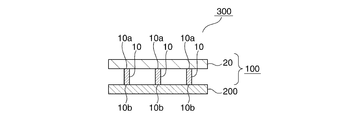
- FIG. 2 is an explanatory diagram of the temporary fixing material with element arranging step (II).
- FIG. 3 is an explanatory diagram of the temporary fixing material peeling step (III).
- FIG. 4 is an explanatory view showing a second embodiment of the method for manufacturing an element mounting board of the present invention.
- the method of manufacturing an element mounting board of the present invention is a method of manufacturing an element mounting board in which elements are mounted on the board. According to the method of manufacturing the element mounting board of the present invention, the element can be mounted with high positional accuracy, so that the yield reduction due to defective mounting position can be eliminated.
- the method for manufacturing an element mounting board of the present invention includes a temporary fixing material preparation step (I), a temporary fixing material placement step (II) and a temporary fixing material peeling step (III).
- the device mounting board manufacturing method of the present invention may include a plurality of device-equipped temporary fixing material preparing steps (I).
- the method for manufacturing an element mounting board of the present invention may include a plurality of element-equipped temporary fixing material arranging steps (II).
- the method for manufacturing an element mounting board of the present invention may include a plurality of temporary fixing material peeling steps (III).
- the method for manufacturing a device mounting board of the present invention includes the provisional fixing material with element preparation step (I), the provisional fixing material with element arranging step (II), and the temporary fixing material removing step (III). Any appropriate other step may be included within the range of not impairing the effect of. For example, a step of forming wiring with a semiconductor photolithography apparatus such as a stepper after mounting the element may be included.
- Temporal fixing material preparation step with element (I) In the temporary fixing material with element preparation step (I), one surface of the element is held on the temporary fixing material to prepare the temporary fixing material with the elements.
- one surface of the element means one surface of two substantially opposite surfaces of the element
- the other surface of the element means that the element is The two surfaces that are substantially opposed to each other mean surfaces that are opposed to the above “one surface of the element”.
- FIG. 1 shows a schematic cross-sectional view of the temporary fixing material with element obtained in the temporary fixing material with element preparing step (I).
- the element-equipped temporary fixing material 100 is arranged such that one surface 10 a of the element 10 is held on the temporary fixing material 20.
- the temporary fixing material with an element may be prepared by any appropriate method as long as it is a method of holding one surface of the element on the temporary fixing material and arranging the elements, without impairing the effects of the present invention. ..
- a film adhesive such as a die attach film is provided on one surface of the element, and the other surface of the element is a suction sheet, a slight adhesive tape, an ultraviolet peeling adhesive tape, Examples thereof include a method of temporarily fixing and arranging on a temporary fixing material such as a heat-peelable adhesive tape.
- FIG. 2 is an explanatory view of the temporary fixing material with element arranging step (II).
- the temporary fixing material with element 100 is arranged so that the other surface 10b of the element 10 is attached onto the substrate 200, and the mounting board with temporary fixing material 300 is obtained.
- a mounting board with a temporary fixing material can be used as long as it is a method of arranging the temporary fixing material with an element on the substrate so that the other surface of the element held by the temporary fixing material with an element adheres to the substrate. It may be produced by any appropriate method as long as the effect of the invention is not impaired. As such a method, for example, the surface provided with a film adhesive such as a die attach film of the elements arranged on the temporary fixing material is bonded to a substrate such as a silicon substrate by adjusting the position. There is a method. Examples of such a bonding method include pressure bonding, pressure reduction bonding, pressure bonding, and heating bonding.
- FIG. 3 shows an explanatory view of the temporary fixing material peeling step (III).
- the temporary fixing material 20 is peeled off from the element mounting board 300 with temporary fixing material obtained in the temporary fixing material with element arranging step (II), and the element mounting board 1000 with the element 10 mounted on the substrate 200 is obtained. can get.
- the element mounting board may be manufactured by any appropriate method as long as it is a method of peeling the temporary fixing material from the element attached on the board, as long as the effect of the present invention is not impaired.
- a method for example, if the temporary fixing material is a suction sheet or a slight adhesive tape, a method such as peeling, if the temporary fixing material is a UV peelable adhesive tape, a method such as ultraviolet irradiation peeling, a temporary fixing material is used.
- a method such as heat peeling can be used.
- One embodiment (Embodiment 1) of the method for manufacturing an element mounting substrate of the present invention uses one type of element and includes a temporary fixing material with element preparing step (I) and a temporary fixing material with element arranging step (II).
- This is a method of manufacturing an element mounting board in which one type of element is mounted on the board by including the temporary fixing material peeling step (III) once each.
- it is an element mounting substrate 1000 in which the element 10 is mounted on a substrate 200 as shown in FIG. In this case, the element 10 is mounted on the substrate 200 with high positional accuracy.
- Emodiment 2 Another embodiment (Embodiment 2) of the method for manufacturing an element mounting substrate of the present invention uses n types (n is an integer of 2 or more) of elements, and a temporary fixing material with element preparation step (I) This is a method of manufacturing an element mounting board in which n kinds of elements are mounted on the board by including the temporary fixing material placement step (II) and the temporary fixing material peeling step (III) each n times.
- FIG. 4 shows an example in which three types of elements are used.
- FIG. 4A is a schematic cross-sectional view of the temporary fixing material with element obtained in the temporary fixing material with element preparing step (I) using the first element 11.
- the temporary fixing material with element 101 in the temporary fixing material with element 101, one surface 11 a of the first element 11 is held on the temporary fixing material 21 and the elements 11 are arranged.
- FIG. 4B is a schematic cross-sectional view of the mounting board with the temporary fixing material, which is obtained in the temporary fixing material with element arranging step (II).
- the temporary fixing material with element 101 is arranged so that the other surface 11b of the element 11 is attached to the substrate 201 in a state of being turned upside down. It is 301.
- FIG. 4C is a schematic sectional view of the element mounting board obtained in the temporary fixing material peeling step (III).
- the element mounting board 1001 is such that the temporary fixing material 21 is peeled from the element mounting board 301 with the temporary fixing material, and the element 11 is mounted on the board 201.
- FIG. 4D is a schematic cross-sectional view of the temporary fixing material with element obtained in the temporary fixing material with element preparing step (I) using the second element 12.
- the temporary fixing material 102 with elements one surface 12 a of the second element 12 is held on the temporary fixing material 22 and the elements 12 are arranged.
- FIG. 4E is a schematic cross-sectional view of the mounting board with temporary fixing material obtained in the temporary fixing material with element arranging step (II).
- the temporary fixing material with element 102 is turned upside down so that the other surface 12b of the element 12 is attached onto the previously obtained element mounting substrate 1001.
- the mounting board 302 with the temporary fixing material is arranged.
- the mounting substrate 302 with the temporary fixing material is manufactured, for example, when the array pattern of the first elements 11 and the array pattern of the second elements 12 are the same, as shown in FIG.
- the first element 11 and the second element 12 can be arranged in the same arrangement pattern by arranging the positions of 1 and 2 so as to deviate from the position of the first element 11.
- FIG. 4F is a schematic cross-sectional view of the element mounting board obtained in the temporary fixing material peeling step (III).
- the element mounting board 1002 is such that the temporary fixing material 22 is peeled from the element mounting board 302 with the temporary fixing material, and the elements 11 and 12 are mounted on the substrate 201.
- the arrangement pattern of the first element 11 and the arrangement pattern of the second element 12 are the same, the position of the second element 12 is arranged so as to be displaced from the position of the first element 11 in the previous step, as described above.
- each of the first element 11 and the second element 12 can be arranged in the same array pattern.
- FIG. 4G is a schematic cross-sectional view of the temporary fixing material with element obtained in the temporary fixing material with element preparing step (I) using the third element 13.
- the temporary fixing material with element 103 in the temporary fixing material with element 103, one surface 13 a of the third element 13 is held on the temporary fixing material 23 and the elements 13 are arranged.
- FIG. 4H is a schematic cross-sectional view of the mounting board with temporary fixing material obtained in the temporary fixing material with element arranging step (II).
- the temporary fixing material with element 103 is turned upside down so that the other surface 13b of the element 13 is attached onto the previously obtained element mounting board 1002.
- the mounting board 303 with the temporary fixing material is arranged.
- FIG. 4( i) is a schematic cross-sectional view of the element mounting board obtained in the temporary fixing material peeling step (III).
- the element mounting board 1003 is obtained by peeling the temporary fixing material 23 from the element mounting board 303 with the temporary fixing material and mounting the elements 11, 12, and 13 on the substrate 201. If the arrangement pattern of the first elements 11, the arrangement pattern of the second elements 12 and the arrangement pattern of the third elements 13 are the same, as described above, the position of the third elements 13 is changed to the first position in the previous step. By disposing the first element 11 and the second element 12 so as to be displaced from the positions, the first element 11, the second element 12, and the third element 13 can be arranged in the same arrangement pattern. ..
- any appropriate elements can be adopted as the three types of elements within a range that does not impair the effects of the present invention.
- an element for example, an R element, a G element, a B element or the like of a micro LED can be adopted. If the second embodiment is carried out by using the R element, G element, and B element of the micro LED by the method for manufacturing the element mounting substrate of the present invention, as shown in FIG. 4(i), the R element of the micro LED is obtained. , G elements, and B elements can be arranged in a regular pattern arrangement with high positional accuracy.
- any appropriate element can be adopted as long as the effect of the present invention is not impaired.
- a semiconductor element is typically used as such an element, and examples thereof include an LED, a micro LED, and a mini LED.
- any suitable size can be adopted as long as the effect of the present invention is not impaired.
- mounting with high positional accuracy can be realized. It is possible to adopt not only a device having a size of a level but also a device having a size of a micro LED having a size of about 3 ⁇ m ⁇ to 30 ⁇ m ⁇ and a thickness of about 1 ⁇ m to 10 ⁇ m.
- an element having a nano level size for example, 1 nm to 1000 nm
- an element having a micro LED level size can be applied.
- the element may be only one type, or may be a plurality of types. It should be noted that even when the color of one element is different (for example, R element, G element, B element of the micro LED), it is treated as a plurality of types of elements.
- Temporal fixing material As the temporary fixing material that can be used in the present invention, any appropriate temporary fixing material can be adopted as long as the effects of the present invention are not impaired.
- a temporary fixing material preferably, one surface of the element can be temporarily held in the element-containing temporary fixing material preparing step (I), and the element-containing temporary fixing material arranging step (II) can be used. The other surface of the element can be placed and attached on the substrate in a state where the element is temporarily held, and can be peeled from the element in the temporary fixing material peeling step (III).
- a temporary fixing material for example, a suction sheet, a slight adhesive tape, a UV peelable adhesive tape, a heat peelable adhesive tape, etc. may be mentioned.
- adsorbent sheet examples include a silicone sheet having adsorbability, a silicone foam sheet, a polyurethane sheet, a polyurethane foam sheet, a polyester sheet, a polyester foam sheet, and the like.
- the ELEP holder series and ELEP mount series manufactured by Nitto Denko Corporation can be mentioned.
- Nitto Denko Corporation's Riva Alpha series etc. can be mentioned.
- the thickness of the temporary fixing material may be any appropriate thickness as long as the effect of the present invention is not impaired.
- Such a thickness is preferably 1 ⁇ m to 800 ⁇ m, more preferably 2 ⁇ m to 500 ⁇ m, further preferably 5 ⁇ m to 200 ⁇ m, and particularly preferably 10 ⁇ m It is 150 ⁇ m.
- the temporary fixing material may be provided with any appropriate other layer on the side opposite to the surface on which the element is temporarily fixed, within a range that does not impair the effects of the present invention.
- any suitable substrate can be used as long as the effects of the present invention are not impaired.
- a substrate include a silicon substrate, a polycrystalline silicon substrate, a sapphire substrate, a silicon carbide substrate, a compound semiconductor (gallium phosphide, gallium arsenide, indium phosphide, gallium nitride) substrate, a glass epoxy substrate, polyimide, etc.
- organic material substrates glass substrates, ceramic substrates, metal substrates, and the like.
- the thickness of the substrate may be any appropriate thickness as long as the effect of the present invention is not impaired.
- a thickness is preferably 10 ⁇ m to 10000 ⁇ m, more preferably 15 ⁇ m to 1000 ⁇ m, further preferably 20 ⁇ m to 500 ⁇ m, particularly preferably 30 ⁇ m It is 300 ⁇ m.
- the substrate may be provided with any appropriate other layer on the side opposite to the surface on which the element is mounted, as long as the effect of the present invention is not impaired.
- ⁇ Mounting position accuracy evaluation method The positional accuracy of the arranged RGB elements was evaluated. When the distance between the RGB elements was within 50 ⁇ m, it was evaluated as ⁇ , and when it was greater than 50 ⁇ m, it was evaluated as x.
- Example 1 A 100 ⁇ m-thick silicone foam sheet having an adsorptive property was attached to the other side of the G element of a 20 ⁇ m size micro LED having a die attach film on one side. Next, the surface of the die attach film was bonded and pressure-bonded to a silicon substrate having a thickness of 150 ⁇ m by adjusting the position. Then, the silicone foam sheet was peeled off. Next, a 100 ⁇ m thick silicone foam sheet having an adsorbing property is attached to the other surface of the R element of the 20 ⁇ m size micro LED having a die attach film on one surface to form a Bayer array as described above. It was bonded to a silicon substrate and pressure-bonded. Then, the silicone foam sheet was peeled off.
- a silicone foam sheet having a thickness of 100 ⁇ m having an adsorbing property is attached to the other face of the B element of a 20 ⁇ m size micro LED having a die attach film on one face, and the above silicon is used so as to form a Bayer array. It was bonded to the substrate and pressure-bonded. Then, the silicone foam sheet was peeled off. As described above, the element mounting board (1) in which the RGB LED elements of the micro LED were arranged on the silicon substrate was obtained. The evaluation result of the mounting position accuracy was ⁇ .
- an element mounting board of the present invention it is possible to provide an element mounting board on which elements are mounted with high positional accuracy. Therefore, for example, manufacturing of an element mounting board on which a miniaturized element such as a micro LED is mounted. It can be used effectively.
Landscapes
- Led Device Packages (AREA)
- Supply And Installment Of Electrical Components (AREA)
- Engineering & Computer Science (AREA)
- Microelectronics & Electronic Packaging (AREA)
Abstract
素子が高い位置精度で実装された素子実装基板の製造方法を提供する。 本発明の素子実装基板の製造方法は、基板上に素子が実装された素子実装基板を製造する方法であって、仮固定材上に素子の一方の面を保持させて該素子を配列させた素子付仮固定材を準備する、素子付仮固定材準備工程(I)と、該素子のもう一方の面が基板上に付着するように、該素子付仮固定材を該基板上に配置する、素子付仮固定材配置工程(II)と、該基板上に付着した該素子から該仮固定材を剥離する仮固定材剥離工程(III)と、を含む。
Description
本発明は、素子実装基板の製造方法に関する。
近年、コスト低減や新たな性能発現等を目的として、LEDなどの各種素子の小型化についての検討がなされている。
LEDは、その一般的な大きさが、500μm□~1000μm□程度、厚みが100μm~200μm程度であり、いわゆる3σ管理で実装する場合は、実装を行うにあたって求められる位置精度は±10μm前後とされている。
LEDなどの各種素子を小型化していくと、高い位置精度での実装が非常に難しくなる。例えば、従来のLEDに比べて大幅に小型化されたマイクロLEDは、一般に、3μm□~30μm□程度、厚みが1μm~10μm程度という微小サイズであり、このような素子を高い位置精度で実装しようとすると、求められる位置精度は±数十nm前後となり、従来の素子実装基板の製造方法では、このような高い位置精度の実装が実現できない。
従来の素子実装基板の製造方法として、例えば、レーザー光の照射による基板への転写を利用した製造方法が報告されている(特許文献1)。しかし、このような製造方法においては、転写の際の空気抵抗の影響によって実装の際の位置ずれが生じるため、高い位置精度の実装を行うことが困難である。
本発明の課題は、素子が高い位置精度で実装された素子実装基板の製造方法を提供することにある。
本発明の素子実装基板の製造方法は、
基板上に素子が実装された素子実装基板を製造する方法であって、
仮固定材上に素子の一方の面を保持させて該素子を配列させた素子付仮固定材を準備する、素子付仮固定材準備工程(I)と、
該素子のもう一方の面が基板上に付着するように、該素子付仮固定材を該基板上に配置する、素子付仮固定材配置工程(II)と、
該基板上に付着した該素子から該仮固定材を剥離する仮固定材剥離工程(III)と、
を含む。
基板上に素子が実装された素子実装基板を製造する方法であって、
仮固定材上に素子の一方の面を保持させて該素子を配列させた素子付仮固定材を準備する、素子付仮固定材準備工程(I)と、
該素子のもう一方の面が基板上に付着するように、該素子付仮固定材を該基板上に配置する、素子付仮固定材配置工程(II)と、
該基板上に付着した該素子から該仮固定材を剥離する仮固定材剥離工程(III)と、
を含む。
一つの実施形態においては、上記素子がLEDチップである。
一つの実施形態においては、上記LEDチップがマイクロLEDチップである。
本発明によれば、素子が高い位置精度で実装された素子実装基板の製造方法を提供できる。
≪本発明の素子実装基板の製造方法の実施形態≫
本発明の素子実装基板の製造方法は、基板上に素子が実装された素子実装基板を製造する方法である。本発明の素子実装基板の製造方法によれば、素子を高い位置精度で実装できるので、実装位置不良による歩留まり低下を解消できる。
本発明の素子実装基板の製造方法は、基板上に素子が実装された素子実装基板を製造する方法である。本発明の素子実装基板の製造方法によれば、素子を高い位置精度で実装できるので、実装位置不良による歩留まり低下を解消できる。
本発明の素子実装基板の製造方法は、素子付仮固定材準備工程(I)と素子付仮固定材配置工程(II)と仮固定材剥離工程(III)とを含む。本発明の素子実装基板の製造方法は、素子付仮固定材準備工程(I)を複数含んでいてもよい。本発明の素子実装基板の製造方法は、素子付仮固定材配置工程(II)を複数含んでいてもよい。本発明の素子実装基板の製造方法は、仮固定材剥離工程(III)を複数含んでいてもよい。本発明の素子実装基板の製造方法は、素子付仮固定材準備工程(I)と素子付仮固定材配置工程(II)と仮固定材剥離工程(III)とを含んでいれば、本発明の効果を損なわない範囲で任意の適切な他の工程を含んでいてもよい。例えば、素子を実装した後に、ステッパー等の半導体フォトリソグラフィー装置で配線を形成する工程を含んでいてもよい。
<素子付仮固定材準備工程(I)>
素子付仮固定材準備工程(I)においては、仮固定材上に素子の一方の面を保持させて該素子を配列させた素子付仮固定材を準備する。
素子付仮固定材準備工程(I)においては、仮固定材上に素子の一方の面を保持させて該素子を配列させた素子付仮固定材を準備する。
なお、本発明の説明において、「素子の一方の面」とは、素子が有する実質的に対向する2つの面の一方の面を意味し、「素子のもう一方の面」とは、素子が有する実質的に対向する2つの面において、上記「素子の一方の面」と対向する面を意味する。
図1に、素子付仮固定材準備工程(I)において得られる素子付仮固定材の概略断面図を示す。図1において、素子付仮固定材100は、仮固定材20の上に素子10の一方の面10aが保持されて該素子10が配列している。
素子付仮固定材は、仮固定材上に素子の一方の面を保持させて該素子を配列させる方法であれば、本発明の効果を損なわない範囲で任意の適切な方法によって準備すればよい。このような方法としては、例えば、素子の一方の面にダイアタッチフィルムなどのフィルム状接着剤を設けるようにし、素子のもう一方の面を、吸着シート、微粘着テープ、紫外線剥離型粘着テープ、熱剥離型粘着テープなどの仮固定材の上に仮固定させて、配列させる方法などが挙げられる。
<素子付仮固定材配置工程(II)>
素子付仮固定材配置工程(II)においては、素子付仮固定材に保持された素子のもう一方の面が基板上に付着するように、素子付仮固定材を該基板上に配置する。図2に、素子付仮固定材配置工程(II)の説明図を示す。図2において、素子付仮固定材100は、素子10のもう一方の面10bが基板200の上に付着するように配置され、仮固定材付実装基板300が得られる。
素子付仮固定材配置工程(II)においては、素子付仮固定材に保持された素子のもう一方の面が基板上に付着するように、素子付仮固定材を該基板上に配置する。図2に、素子付仮固定材配置工程(II)の説明図を示す。図2において、素子付仮固定材100は、素子10のもう一方の面10bが基板200の上に付着するように配置され、仮固定材付実装基板300が得られる。
仮固定材付実装基板は、素子付仮固定材に保持された素子のもう一方の面が基板上に付着するように、素子付仮固定材を該基板上に配置させる方法であれば、本発明の効果を損なわない範囲で任意の適切な方法によって作製すればよい。このような方法としては、例えば、仮固定材の上に配列させた素子のダイアタッチフィルムなどのフィルム状接着剤が設けられた面を、シリコン基板などの基板に、位置を調整して貼り合せる方法が挙げられる。このような貼り合せる方法としては、例えば、圧着での貼り合わせや、減圧での貼り合わせや、加圧での貼り合わせや、加熱での貼り合わせなどが挙げられる。
<仮固定材剥離工程(III)>
仮固定材剥離工程(III)においては、基板上に付着した素子から仮固定材を剥離する。図3に、仮固定材剥離工程(III)の説明図を示す。図3において、素子付仮固定材配置工程(II)によって得られる仮固定材付素子実装基板300から、仮固定材20が剥離され、基板200上に素子10が実装された素子実装基板1000が得られる。
仮固定材剥離工程(III)においては、基板上に付着した素子から仮固定材を剥離する。図3に、仮固定材剥離工程(III)の説明図を示す。図3において、素子付仮固定材配置工程(II)によって得られる仮固定材付素子実装基板300から、仮固定材20が剥離され、基板200上に素子10が実装された素子実装基板1000が得られる。
素子実装基板は、基板上に付着した素子から仮固定材を剥離する方法であれば、本発明の効果を損なわない範囲で任意の適切な方法によって作製すればよい。このような方法としては、例えば、仮固定材が吸着シートや微粘着テープであればピールなどの方法、仮固定材が紫外線剥離型粘着テープであれば紫外線照射剥離などの方法、仮固定材が熱剥離型粘着テープであれば加熱剥離などの方法、などが挙げられる。
<実施形態1>
本発明の素子実装基板の製造方法の一つの実施形態(実施形態1)は、1種の素子を用い、素子付仮固定材準備工程(I)と素子付仮固定材配置工程(II)と仮固定材剥離工程(III)とをそれぞれ1回ずつ含むことにより、基板上に1種の素子が実装された素子実装基板を製造する方法である。代表的には、図3に示すような、基板200上に素子10が実装された素子実装基板1000である。この場合、基板200上に素子10が高い位置精度で実装される。
本発明の素子実装基板の製造方法の一つの実施形態(実施形態1)は、1種の素子を用い、素子付仮固定材準備工程(I)と素子付仮固定材配置工程(II)と仮固定材剥離工程(III)とをそれぞれ1回ずつ含むことにより、基板上に1種の素子が実装された素子実装基板を製造する方法である。代表的には、図3に示すような、基板200上に素子10が実装された素子実装基板1000である。この場合、基板200上に素子10が高い位置精度で実装される。
<実施形態2>
本発明の素子実装基板の製造方法の別の一つの実施形態(実施形態2)は、n種類(nは2以上の整数)の素子を用い、素子付仮固定材準備工程(I)と素子付仮固定材配置工程(II)と仮固定材剥離工程(III)とをそれぞれn回ずつ含むことにより、基板上にn種類の素子が実装された素子実装基板を製造する方法である。
本発明の素子実装基板の製造方法の別の一つの実施形態(実施形態2)は、n種類(nは2以上の整数)の素子を用い、素子付仮固定材準備工程(I)と素子付仮固定材配置工程(II)と仮固定材剥離工程(III)とをそれぞれn回ずつ含むことにより、基板上にn種類の素子が実装された素子実装基板を製造する方法である。
実施形態2について、図4を用いて具体的に説明する。図4は、3種類の素子を用いた場合の例である。
図4(a)は、第1の素子11を用いて素子付仮固定材準備工程(I)において得られる素子付仮固定材の概略断面図である。図4(a)において、素子付仮固定材101は、仮固定材21の上に第1の素子11の一方の面11aが保持されて該素子11が配列している。
図4(b)は、素子付仮固定材配置工程(II)において得られる仮固定材付実装基板の概略断面図である。図4(b)において、素子付仮固定材101は、上下が反転された状態で、素子11のもう一方の面11bが基板201の上に付着するように配置され、仮固定材付実装基板301となっている。
図4(c)は、仮固定材剥離工程(III)において得られる素子実装基板の概略断面図である。図4(c)において、素子実装基板1001は、仮固定材付素子実装基板301から仮固定材21が剥離され、基板201上に素子11が実装されたものとなっている。
図4(d)は、第2の素子12を用いて素子付仮固定材準備工程(I)において得られる素子付仮固定材の概略断面図である。図4(d)において、素子付仮固定材102は、仮固定材22の上に第2の素子12の一方の面12aが保持されて該素子12が配列している。
図4(e)は、素子付仮固定材配置工程(II)において得られる仮固定材付実装基板の概略断面図である。図4(e)において、素子付仮固定材102は、上下が反転された状態で、素子12のもう一方の面12bが、先に得られている素子実装基板1001の上に付着するように配置され、仮固定材付実装基板302となっている。この仮固定材付実装基板302を作製するに際し、例えば、第1の素子11の配列パターンと第2の素子12の配列パターンが同じ場合、図4(e)のように、第2の素子12の位置を第1の素子11の位置とずれるように配置させることにより、第1の素子11と第2の素子12のそれぞれを同じ配列パターンで並ばせることができる。
図4(f)は、仮固定材剥離工程(III)において得られる素子実装基板の概略断面図である。図4(f)において、素子実装基板1002は、仮固定材付素子実装基板302から仮固定材22が剥離され、基板201上に素子11と素子12が実装されたものとなっており、第1の素子11の配列パターンと第2の素子12の配列パターンが同じ場合、上述の通り、先の工程において、第2の素子12の位置を第1の素子11の位置とずれるように配置させることにより、第1の素子11と第2の素子12のそれぞれを同じ配列パターンで並ばせることができる。
図4(g)は、第3の素子13を用いて素子付仮固定材準備工程(I)において得られる素子付仮固定材の概略断面図である。図4(g)において、素子付仮固定材103は、仮固定材23の上に第3の素子13の一方の面13aが保持されて該素子13が配列している。
図4(h)は、素子付仮固定材配置工程(II)において得られる仮固定材付実装基板の概略断面図である。図4(h)において、素子付仮固定材103は、上下が反転された状態で、素子13のもう一方の面13bが、先に得られている素子実装基板1002の上に付着するように配置され、仮固定材付実装基板303となっている。この仮固定材付実装基板303を作製するに際し、例えば、第1の素子11の配列パターンと第2の素子12の配列パターンと第3の素子13の配列パターンが同じ場合、図4(h)のように、第3の素子13の位置を第1の素子11および第2の素子12の位置とずれるように配置させることにより、第1の素子11と第2の素子12と第3の素子13のそれぞれを同じ配列パターンで並ばせることができる。
図4(i)は、仮固定材剥離工程(III)において得られる素子実装基板の概略断面図である。図4(i)において、素子実装基板1003は、仮固定材付素子実装基板303から仮固定材23が剥離され、基板201上に素子11と素子12と素子13が実装されたものとなっており、第1の素子11の配列パターンと第2の素子12の配列パターンと第3の素子13の配列パターンが同じ場合、上述の通り、先の工程において、第3の素子13の位置を第1の素子11および第2の素子12の位置とずれるように配置させることにより、第1の素子11と第2の素子12と第3の素子13のそれぞれを同じ配列パターンで並ばせることができる。
実施形態2について、例えば、図4で示すように3種類の素子を用いる場合、それら3種類の素子としては、本発明の効果を損なわない範囲で、任意の適切な素子を採用し得る。このような素子としては、例えば、マイクロLEDのR素子、G素子、B素子などが採用され得る。本発明の素子実装基板の製造方法によって、マイクロLEDのR素子、G素子、B素子を用いて、実施形態2を実施すれば、図4(i)に示されるように、マイクロLEDのR素子、G素子、B素子を、高い位置精度で、規則的なパターン配列で配置させることができる。
<素子>
本発明において採用し得る素子としては、本発明の効果を損なわない範囲で、任意の適切な素子を採用し得る。このような素子としては、代表的には半導体素子であり、例えば、LED、マイクロLED、ミニLEDなどが挙げられる。
本発明において採用し得る素子としては、本発明の効果を損なわない範囲で、任意の適切な素子を採用し得る。このような素子としては、代表的には半導体素子であり、例えば、LED、マイクロLED、ミニLEDなどが挙げられる。
本発明において採用し得る素子の大きさとしては、本発明の効果を損なわない範囲で、任意の適切な大きさを採用し得る。本発明においては、小型化された素子を採用しても高い位置精度の実装が実現できるので、500μm□~1000μm□程度のLEDレベルの大きさの素子や、厚みが100μm~200μm程度のミニLEDレベルの大きさの素子はもちろんのこと、3μm□~30μm□程度、厚みが1μm~10μm程度のマイクロLEDレベルの大きさの素子も採用し得る。また、本発明の素子実装基板の製造方法であれば、マイクロLEDレベルの大きさの素子よりもさらに小さいナノレベルの大きさ(例えば、1nm~1000nmなど)の素子も適用可能である。
素子は、1種類のみであってもよいし、複数の種類であってもよい。なお、1つの素子において色の異なる場合(例えば、マイクロLEDのR素子、G素子、B素子など)も複数の種類の素子として扱う。
<仮固定材>
本発明において採用し得る仮固定材としては、本発明の効果を損なわない範囲で、任意の適切な仮固定材を採用し得る。このような仮固定材としては、好ましくは、素子付仮固定材準備工程(I)において素子の一方の面を一時的に保持させることができ、素子付仮固定材配置工程(II)において素子を一時的に保持させた状態で該素子のもう一方の面を基板上に配置および付着させることができ、仮固定材剥離工程(III)において素子から剥離できるものである。
本発明において採用し得る仮固定材としては、本発明の効果を損なわない範囲で、任意の適切な仮固定材を採用し得る。このような仮固定材としては、好ましくは、素子付仮固定材準備工程(I)において素子の一方の面を一時的に保持させることができ、素子付仮固定材配置工程(II)において素子を一時的に保持させた状態で該素子のもう一方の面を基板上に配置および付着させることができ、仮固定材剥離工程(III)において素子から剥離できるものである。
このような仮固定材としては、例えば、吸着シート、微粘着テープ、紫外線剥離型粘着テープ、熱剥離型粘着テープなどが挙げられる。
吸着シートとしては、例えば、吸着性を有するシリコーンシート、シリコーン発泡シート、ポリウレタンシート、ポリウレタン発泡シート、ポリエステルシート、ポリエステル発泡シートなどが挙げられる。
微粘着テープであれば、日東電工株式会社製のSPVシリーズ、E-MASKシリーズ、エレップマスキングシリーズなどが挙げられる。
紫外線剥離型粘着テープであれば、日東電工株式会社製のエレップホルダーシリーズ、エレップマウントシリーズなどが挙げられる。
熱剥離型粘着テープであれば、日東電工株式会社製のリバアルファシリーズなどが挙げられる。
仮固定材の厚みは、本発明の効果を損なわない範囲で、任意の適切な厚みを採用し得る。このような厚みとしては、本発明の効果をより発現させ得る点で、好ましくは1μm~800μmであり、より好ましくは2μm~500μmであり、さらに好ましくは5μm~200μmであり、特に好ましくは10μm~150μmである。
仮固定材は、素子を仮固定させる面と反対側に、本発明の効果を損なわない範囲で任意の適切な他の層が備えられていてもよい。
<基板>
本発明において採用し得る基板としては、本発明の効果を損なわない範囲で、任意の適切な基板を採用し得る。このような基板としては、例えば、シリコン基板、多結晶シリコン基板、サファイヤ基板、シリコンカーバイド基板、化合物半導体(リン化ガリウム、ヒ化ガリウム、リン化インジウム、窒化ガリウム)基板、ガラスエポキシ基板、ポリイミドなどの有機材料基板、ガラス基板、セラミック基板、金属基板などが挙げられる。
本発明において採用し得る基板としては、本発明の効果を損なわない範囲で、任意の適切な基板を採用し得る。このような基板としては、例えば、シリコン基板、多結晶シリコン基板、サファイヤ基板、シリコンカーバイド基板、化合物半導体(リン化ガリウム、ヒ化ガリウム、リン化インジウム、窒化ガリウム)基板、ガラスエポキシ基板、ポリイミドなどの有機材料基板、ガラス基板、セラミック基板、金属基板などが挙げられる。
基板の厚みは、本発明の効果を損なわない範囲で、任意の適切な厚みを採用し得る。このような厚みとしては、本発明の効果をより発現させ得る点で、好ましくは10μm~10000μmであり、より好ましくは15μm~1000μmであり、さらに好ましくは20μm~500μmであり、特に好ましくは30μm~300μmである。
基板は、素子を実装させる面と反対側に、本発明の効果を損なわない範囲で任意の適切な他の層が備えられていてもよい。
以下、実施例により本発明を具体的に説明するが、本発明はこれら実施例になんら限定されるものではない。なお、実施例等における、試験および評価方法は以下のとおりである。なお、「部」と記載されている場合は、特記事項がない限り「質量部」を意味し、「%」と記載されている場合は、特記事項がない限り「質量%」を意味する。
<実装の位置精度の評価方法>
配列したRGB素子の位置精度を評価した。RGB素子間の距離が50μm以内であれば○、50μmより大きいと×とした。
配列したRGB素子の位置精度を評価した。RGB素子間の距離が50μm以内であれば○、50μmより大きいと×とした。
〔実施例1〕
一方の面にダイアタッチフィルムを設けた20μmサイズのマイクロLEDのG素子のもう一方の面に、吸着性を有する厚み100μmのシリコーン発泡シートを貼り合せた。次に、厚み150μmのシリコン基板に、位置を調整してダイアタッチフィルムの面を貼り合せて圧着した。その後、シリコーン発泡シートをピール剥離した。
次に、一方の面にダイアタッチフィルムを設けた20μmサイズのマイクロLEDのR素子のもう一方の面に、吸着性を有する厚み100μmのシリコーン発泡シートを貼り合せ、ベイヤー配列となるように、上記シリコン基板に貼り合せて圧着した。その後、シリコーン発泡シートをピール剥離した。
さらに、一方の面にダイアタッチフィルムを設けた20μmサイズのマイクロLEDのB素子のもう一方の面に、吸着性を有する厚み100μmのシリコーン発泡シートを貼り合せ、ベイヤー配列となるように、上記シリコン基板に貼り合せて圧着した。その後、シリコーン発泡シートをピール剥離した。
以上のようにして、シリコン基板上にマイクロLEDのRGB素子が配列した素子実装基板(1)を得た。
実装の位置精度の評価結果は○であった。
一方の面にダイアタッチフィルムを設けた20μmサイズのマイクロLEDのG素子のもう一方の面に、吸着性を有する厚み100μmのシリコーン発泡シートを貼り合せた。次に、厚み150μmのシリコン基板に、位置を調整してダイアタッチフィルムの面を貼り合せて圧着した。その後、シリコーン発泡シートをピール剥離した。
次に、一方の面にダイアタッチフィルムを設けた20μmサイズのマイクロLEDのR素子のもう一方の面に、吸着性を有する厚み100μmのシリコーン発泡シートを貼り合せ、ベイヤー配列となるように、上記シリコン基板に貼り合せて圧着した。その後、シリコーン発泡シートをピール剥離した。
さらに、一方の面にダイアタッチフィルムを設けた20μmサイズのマイクロLEDのB素子のもう一方の面に、吸着性を有する厚み100μmのシリコーン発泡シートを貼り合せ、ベイヤー配列となるように、上記シリコン基板に貼り合せて圧着した。その後、シリコーン発泡シートをピール剥離した。
以上のようにして、シリコン基板上にマイクロLEDのRGB素子が配列した素子実装基板(1)を得た。
実装の位置精度の評価結果は○であった。
〔比較例1〕
仮固定材として、粘着力が大きいNo.375(日東電工株式会社製、包装用OPPテープ)を用いた以外は、実施例1と同様に行ったところ、シリコン基板上にマイクロLEDのRGB素子を配列することができなかった。
仮固定材として、粘着力が大きいNo.375(日東電工株式会社製、包装用OPPテープ)を用いた以外は、実施例1と同様に行ったところ、シリコン基板上にマイクロLEDのRGB素子を配列することができなかった。
本発明の素子実装基板の製造方法によれば、素子が高い位置精度で実装された素子実装基板を提供できるので、例えば、マイクロLEDなどの小型化された素子が実装された素子実装基板の製造に有効に利用可能である。
Claims (3)
- 基板上に素子が実装された素子実装基板を製造する方法であって、
仮固定材上に素子の一方の面を保持させて該素子を配列させた素子付仮固定材を準備する、素子付仮固定材準備工程(I)と、
該素子のもう一方の面が基板上に付着するように、該素子付仮固定材を該基板上に配置する、素子付仮固定材配置工程(II)と、
該基板上に付着した該素子から該仮固定材を剥離する仮固定材剥離工程(III)と、
を含む、
素子実装基板の製造方法。 - 前記素子がLEDチップである、請求項1に記載の素子実装基板の製造方法。
- 前記LEDチップがマイクロLEDチップである、請求項2に記載の素子実装基板の製造方法。
Priority Applications (3)
| Application Number | Priority Date | Filing Date | Title |
|---|---|---|---|
| CN201980093144.7A CN113474901A (zh) | 2019-02-26 | 2019-12-03 | 元件安装基板的制造方法 |
| US17/421,798 US20220093816A1 (en) | 2019-02-26 | 2019-12-03 | Method for manufacturing element mounting substrate |
| KR1020217026673A KR102937507B1 (ko) | 2019-02-26 | 2019-12-03 | 소자 실장 기판의 제조 방법 |
Applications Claiming Priority (2)
| Application Number | Priority Date | Filing Date | Title |
|---|---|---|---|
| JP2019033021A JP7266947B2 (ja) | 2019-02-26 | 2019-02-26 | 素子実装基板の製造方法 |
| JP2019-033021 | 2019-02-26 |
Publications (1)
| Publication Number | Publication Date |
|---|---|
| WO2020174797A1 true WO2020174797A1 (ja) | 2020-09-03 |
Family
ID=72239031
Family Applications (1)
| Application Number | Title | Priority Date | Filing Date |
|---|---|---|---|
| PCT/JP2019/047142 Ceased WO2020174797A1 (ja) | 2019-02-26 | 2019-12-03 | 素子実装基板の製造方法 |
Country Status (6)
| Country | Link |
|---|---|
| US (1) | US20220093816A1 (ja) |
| JP (1) | JP7266947B2 (ja) |
| KR (1) | KR102937507B1 (ja) |
| CN (1) | CN113474901A (ja) |
| TW (1) | TWI837243B (ja) |
| WO (1) | WO2020174797A1 (ja) |
Families Citing this family (1)
| Publication number | Priority date | Publication date | Assignee | Title |
|---|---|---|---|---|
| CN114156259A (zh) * | 2020-09-08 | 2022-03-08 | 致伸科技股份有限公司 | 光源模块及其制造方法 |
Citations (4)
| Publication number | Priority date | Publication date | Assignee | Title |
|---|---|---|---|---|
| JP2010251360A (ja) * | 2009-04-10 | 2010-11-04 | Sony Corp | 表示装置の製造方法および表示装置 |
| WO2017124332A1 (en) * | 2016-01-20 | 2017-07-27 | Goertek.Inc | Micro-led transfer method and manufacturing method |
| JP2018074024A (ja) * | 2016-10-31 | 2018-05-10 | 凸版印刷株式会社 | 透光性無機led光源シート及びその製造方法並びに複合面状発光体 |
| US20190058081A1 (en) * | 2017-08-18 | 2019-02-21 | Khaled Ahmed | Micro light-emitting diode (led) display and assembly apparatus |
Family Cites Families (11)
| Publication number | Priority date | Publication date | Assignee | Title |
|---|---|---|---|---|
| JP2003077940A (ja) | 2001-09-06 | 2003-03-14 | Sony Corp | 素子の転写方法及びこれを用いた素子の配列方法、画像表示装置の製造方法 |
| KR101033797B1 (ko) * | 2003-01-15 | 2011-05-13 | 가부시키가이샤 한도오따이 에네루기 켄큐쇼 | 박리 방법 및 그 박리 방법을 사용한 표시 장치의 제작 방법 |
| JP2010161221A (ja) | 2009-01-08 | 2010-07-22 | Sony Corp | 実装基板の製造方法、実装基板および発光装置 |
| JP2016082235A (ja) | 2014-10-09 | 2016-05-16 | 古河電気工業株式会社 | Led発光素子パッケージの発泡樹脂金属被覆複合シート基板への実装構造とled照明器具用の発泡樹脂金属被覆複合シート基板 |
| JP6395597B2 (ja) * | 2014-12-25 | 2018-09-26 | マクセルホールディングス株式会社 | ダイシング用粘着テープおよび半導体チップの製造方法 |
| KR101754528B1 (ko) * | 2016-03-23 | 2017-07-06 | 한국광기술원 | 건식 접착구조를 갖는 led 구조체 어레이의 전사체와 이를 이용한 led 구조체 어레이의 이송방법 및 led 구조체 |
| JP6666778B2 (ja) * | 2016-04-06 | 2020-03-18 | 日東電工株式会社 | 吸着仮固定材 |
| US10002856B1 (en) * | 2017-01-26 | 2018-06-19 | International Business Machines Corporation | Micro-LED array transfer |
| JP6934313B2 (ja) * | 2017-04-05 | 2021-09-15 | 日東電工株式会社 | 吸着仮固定シートおよびその製造方法 |
| TWI647831B (zh) * | 2017-08-09 | 2019-01-11 | 英屬開曼群島商錼創科技股份有限公司 | 微型發光二極體裝置及其製作方法 |
| CN111063649B (zh) * | 2019-12-03 | 2022-11-01 | 深圳市华星光电半导体显示技术有限公司 | Micro LED的转移方法及转移装置 |
-
2019
- 2019-02-26 JP JP2019033021A patent/JP7266947B2/ja active Active
- 2019-12-03 WO PCT/JP2019/047142 patent/WO2020174797A1/ja not_active Ceased
- 2019-12-03 KR KR1020217026673A patent/KR102937507B1/ko active Active
- 2019-12-03 CN CN201980093144.7A patent/CN113474901A/zh active Pending
- 2019-12-03 US US17/421,798 patent/US20220093816A1/en not_active Abandoned
- 2019-12-11 TW TW108145374A patent/TWI837243B/zh active
Patent Citations (4)
| Publication number | Priority date | Publication date | Assignee | Title |
|---|---|---|---|---|
| JP2010251360A (ja) * | 2009-04-10 | 2010-11-04 | Sony Corp | 表示装置の製造方法および表示装置 |
| WO2017124332A1 (en) * | 2016-01-20 | 2017-07-27 | Goertek.Inc | Micro-led transfer method and manufacturing method |
| JP2018074024A (ja) * | 2016-10-31 | 2018-05-10 | 凸版印刷株式会社 | 透光性無機led光源シート及びその製造方法並びに複合面状発光体 |
| US20190058081A1 (en) * | 2017-08-18 | 2019-02-21 | Khaled Ahmed | Micro light-emitting diode (led) display and assembly apparatus |
Also Published As
| Publication number | Publication date |
|---|---|
| TW202032818A (zh) | 2020-09-01 |
| KR102937507B1 (ko) | 2026-03-11 |
| US20220093816A1 (en) | 2022-03-24 |
| KR20210129065A (ko) | 2021-10-27 |
| JP2020140978A (ja) | 2020-09-03 |
| TWI837243B (zh) | 2024-04-01 |
| JP7266947B2 (ja) | 2023-05-01 |
| CN113474901A (zh) | 2021-10-01 |
Similar Documents
| Publication | Publication Date | Title |
|---|---|---|
| US20080220566A1 (en) | Substrate process for an embedded component | |
| KR101219619B1 (ko) | 웨이퍼 레벨에서의 반도체 패키징 방법 | |
| JP6207151B2 (ja) | ドライ・フィルム・フォトレジストを使用したダイ上部への蛍光体の堆積 | |
| US20130210179A1 (en) | Printing phosphor on led wafer using dry film lithography | |
| TW201227937A (en) | Image sensor chip package and method for forming the same | |
| WO2007106625A2 (en) | Perforated embedded plane package and method | |
| TW202105585A (zh) | 半導體晶片之支持基板、轉印裝置及轉印方法 | |
| KR20200035236A (ko) | 이미지 센서 모듈 및 이의 제조 방법 | |
| US20100144096A1 (en) | Method of manufacturing semiconductor device in which bottom surface and side surface of semiconductor substrate are covered with resin protective film | |
| WO2020174797A1 (ja) | 素子実装基板の製造方法 | |
| CN113571494B (zh) | 电子装置及其制作方法 | |
| JP2004219964A (ja) | 画素制御素子の選択転写方法、及び、画素制御素子の選択転写方法に使用される画素制御素子の実装装置 | |
| JP2026035896A (ja) | 電子構造体、電子回路の製造方法及び電子構造体の製造方法 | |
| TW202221837A (zh) | 晶片部件之轉移裝置 | |
| KR102587996B1 (ko) | 반도체 소자의 전사 방법 | |
| KR20190036161A (ko) | 플렉서블 전자 소자 제작을 위한 전사 장비 및 이를 이용한 전사 방법 | |
| CN102484106A (zh) | 用于制造集成电路的方法和产生的膜芯片 | |
| CN116936446A (zh) | 临时载板结构、临时载板结构的制备方法及芯片转移方法 | |
| JP7739964B2 (ja) | 電子構造体及び電子回路の製造方法 | |
| WO2014150263A1 (en) | Printing phosphor on led wafer using dry film lithography | |
| TW202209540A (zh) | 在基板系統之間轉移對準標記的方法和系統 | |
| JP2012054331A (ja) | 固体撮像装置の製造方法 | |
| CN101202234A (zh) | 芯片重布工具结构及其方法 | |
| TW202349565A (zh) | 電子裝置及其製造方法 | |
| JP2003152134A (ja) | チップ状電子部品の製造方法、及びその製造に用いる疑似ウェーハの製造方法 |
Legal Events
| Date | Code | Title | Description |
|---|---|---|---|
| 121 | Ep: the epo has been informed by wipo that ep was designated in this application |
Ref document number: 19917043 Country of ref document: EP Kind code of ref document: A1 |
|
| NENP | Non-entry into the national phase |
Ref country code: DE |
|
| 122 | Ep: pct application non-entry in european phase |
Ref document number: 19917043 Country of ref document: EP Kind code of ref document: A1 |