WO2020170855A1 - 半導体デバイスおよび半導体装置 - Google Patents
半導体デバイスおよび半導体装置 Download PDFInfo
- Publication number
- WO2020170855A1 WO2020170855A1 PCT/JP2020/004789 JP2020004789W WO2020170855A1 WO 2020170855 A1 WO2020170855 A1 WO 2020170855A1 JP 2020004789 W JP2020004789 W JP 2020004789W WO 2020170855 A1 WO2020170855 A1 WO 2020170855A1
- Authority
- WO
- WIPO (PCT)
- Prior art keywords
- semiconductor device
- semiconductor
- substrate
- semiconductor substrate
- grooves
- Prior art date
- Legal status (The legal status is an assumption and is not a legal conclusion. Google has not performed a legal analysis and makes no representation as to the accuracy of the status listed.)
- Ceased
Links
Images










Classifications
-
- H—ELECTRICITY
- H10—SEMICONDUCTOR DEVICES; ELECTRIC SOLID-STATE DEVICES NOT OTHERWISE PROVIDED FOR
- H10H—INORGANIC LIGHT-EMITTING SEMICONDUCTOR DEVICES HAVING POTENTIAL BARRIERS
- H10H20/00—Individual inorganic light-emitting semiconductor devices having potential barriers, e.g. light-emitting diodes [LED]
- H10H20/80—Constructional details
- H10H20/81—Bodies
- H10H20/819—Bodies characterised by their shape, e.g. curved or truncated substrates
-
- H—ELECTRICITY
- H10—SEMICONDUCTOR DEVICES; ELECTRIC SOLID-STATE DEVICES NOT OTHERWISE PROVIDED FOR
- H10W—GENERIC PACKAGES, INTERCONNECTIONS, CONNECTORS OR OTHER CONSTRUCTIONAL DETAILS OF DEVICES COVERED BY CLASS H10
- H10W72/00—Interconnections or connectors in packages
-
- H—ELECTRICITY
- H10—SEMICONDUCTOR DEVICES; ELECTRIC SOLID-STATE DEVICES NOT OTHERWISE PROVIDED FOR
- H10H—INORGANIC LIGHT-EMITTING SEMICONDUCTOR DEVICES HAVING POTENTIAL BARRIERS
- H10H20/00—Individual inorganic light-emitting semiconductor devices having potential barriers, e.g. light-emitting diodes [LED]
- H10H20/80—Constructional details
- H10H20/85—Packages
- H10H20/857—Interconnections, e.g. lead-frames, bond wires or solder balls
-
- H—ELECTRICITY
- H10—SEMICONDUCTOR DEVICES; ELECTRIC SOLID-STATE DEVICES NOT OTHERWISE PROVIDED FOR
- H10W—GENERIC PACKAGES, INTERCONNECTIONS, CONNECTORS OR OTHER CONSTRUCTIONAL DETAILS OF DEVICES COVERED BY CLASS H10
- H10W74/00—Encapsulations, e.g. protective coatings
- H10W74/01—Manufacture or treatment
-
- H—ELECTRICITY
- H10—SEMICONDUCTOR DEVICES; ELECTRIC SOLID-STATE DEVICES NOT OTHERWISE PROVIDED FOR
- H10W—GENERIC PACKAGES, INTERCONNECTIONS, CONNECTORS OR OTHER CONSTRUCTIONAL DETAILS OF DEVICES COVERED BY CLASS H10
- H10W90/00—Package configurations
-
- H—ELECTRICITY
- H10—SEMICONDUCTOR DEVICES; ELECTRIC SOLID-STATE DEVICES NOT OTHERWISE PROVIDED FOR
- H10H—INORGANIC LIGHT-EMITTING SEMICONDUCTOR DEVICES HAVING POTENTIAL BARRIERS
- H10H20/00—Individual inorganic light-emitting semiconductor devices having potential barriers, e.g. light-emitting diodes [LED]
- H10H20/80—Constructional details
- H10H20/85—Packages
- H10H20/852—Encapsulations
-
- H—ELECTRICITY
- H10—SEMICONDUCTOR DEVICES; ELECTRIC SOLID-STATE DEVICES NOT OTHERWISE PROVIDED FOR
- H10W—GENERIC PACKAGES, INTERCONNECTIONS, CONNECTORS OR OTHER CONSTRUCTIONAL DETAILS OF DEVICES COVERED BY CLASS H10
- H10W90/00—Package configurations
- H10W90/701—Package configurations characterised by the relative positions of pads or connectors relative to package parts
- H10W90/721—Package configurations characterised by the relative positions of pads or connectors relative to package parts of bump connectors
- H10W90/724—Package configurations characterised by the relative positions of pads or connectors relative to package parts of bump connectors between a chip and a stacked insulating package substrate, interposer or RDL
Definitions
- the present disclosure relates to a semiconductor device mounted on a substrate using bumps and a semiconductor device including the semiconductor device.
- Patent Document 1 discloses a semiconductor device in which an adhesive pattern with a resin fillet is improved by providing a concave-convex pattern on the end surface of the chip to increase the adhesive strength between the chip and the substrate.
- a first semiconductor device is a semiconductor substrate having one surface and another surface facing each other and one side of which is 50 ⁇ m or more and 500 ⁇ m or less, and one or a plurality of bumps provided on the other surface. And a concavo-convex structure formed on the side surface of the semiconductor substrate.
- a first semiconductor device is one in which a plurality of semiconductor devices are mounted on a mounting board, and the first semiconductor device according to the above embodiment is provided as the plurality of semiconductor devices. Is.
- a second semiconductor device is a semiconductor substrate having one surface and another surface facing each other, one or a plurality of bumps provided on the other surface, and a dry etching on a side surface of the semiconductor substrate. And an uneven structure formed by.
- a second semiconductor device is one in which a plurality of semiconductor devices are mounted on a mounting substrate, and the second semiconductor device according to the embodiment is provided as the plurality of semiconductor devices. Is.
- the first semiconductor device of one embodiment, the second semiconductor device of one embodiment, and the second semiconductor device of one embodiment semiconductor elements are arranged.
- An uneven structure was formed on the side surface of the semiconductor substrate by dry etching. This increases the surface tension on the side surface of the semiconductor substrate.
- FIG. 9 is a schematic cross sectional view for illustrating the method for manufacturing the semiconductor device shown in FIG. 1.
- FIG. 3 is a perspective view showing an example of the overall configuration of the semiconductor device (image display device) shown in FIG. 1.
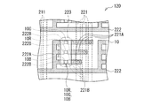
- FIG. 7 is a schematic diagram showing an example of a wiring layout of the image display device shown in FIG. 6. It is a cross-sectional schematic diagram showing an example of a structure of the mounting board shown in FIG.
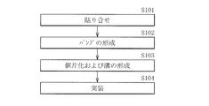
- FIG. 10 is a flowchart showing a manufacturing process of a semiconductor device according to a modified example of the present disclosure.
- Embodiment an example of a semiconductor device having a groove on a side surface of a chip substrate
- Configuration of semiconductor device 1-2 Configuration of semiconductor device 1-2.
- Manufacturing method of semiconductor device 1-3 Configuration of semiconductor device 1-4.
- Actions and effects 2.
- Modified example Example of semiconductor device in which the side surface of the chip substrate is hydrophilized
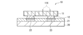
- FIG. 1 illustrates a cross-sectional configuration of a semiconductor device (semiconductor device 10) according to an embodiment of the present disclosure.
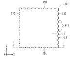
- FIG. 2 shows a planar configuration of the semiconductor device 10 shown in FIG. Note that FIG. 1 shows a cross section taken along the line II shown in FIG. 2, for example.
- the semiconductor device 10 has one or a plurality of bumps 12 on a surface S2 of a semiconductor substrate 11 having one surface (surface S1) and the other surface (surface S2) facing each other, and further, a side surface (surface) of the semiconductor substrate 11.
- a plurality of grooves 11X are formed in S3) as an uneven structure.
- 1 and 2 schematically show the configuration of the semiconductor device 10, and may differ from the actual dimensions and shape.
- the semiconductor device 10 is, for example, a semiconductor chip having a side of 50 ⁇ m or more and 500 ⁇ m or less, more specifically, a side of 80 ⁇ m or more and 200 ⁇ m.
- the semiconductor device 10 is, for example, an LED chip that is preferably used as a display pixel of an image display device called a so-called LED (Light Emitting Diode) display.
- the LED chip corresponds to a specific but not limitative example of “semiconductor device” of the present disclosure.
- the semiconductor device 10 is provided with the plurality of grooves 11X on the side surface (surface S3) of the semiconductor substrate 11.
- the plurality of grooves 11X are for assisting the contact between the bumps 12 and the electrodes 22 on the mounting substrate 20 side during mounting on the mounting substrate 20 by flux reflow (see, for example, FIG. 5E). ).
- the plurality of grooves 11X are provided on the side surface (surface S3) of the semiconductor substrate 11. This increases the surface area of the semiconductor device 10 and facilitates contact between the bumps 12 of the semiconductor device 10 and the mounting electrodes 22 on the mounting substrate 20 side during flux reflow.
- An anti-oxidation film 23 made of, for example, gold (Au) plating is provided on the electrode 22.
- the plurality of grooves 11X extend parallel to each other in the normal direction (eg, the Y-axis direction) to the facing surfaces S1 and S2.
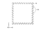
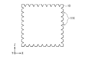
- the cross section of the plurality of grooves 11X in the horizontal direction (for example, the XZ plane direction) with respect to the surface S1 and the surface S2 has a substantially semicircular shape as shown in FIG. 2, but is not limited thereto. Since the plurality of grooves 11X are for increasing the surface area of the semiconductor device 10 as described above, for example, the substantially rectangular shape as shown in FIG. 3A or the substantially triangular shape as shown in FIG. 3B.
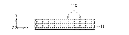
- the plurality of grooves 11X linearly extending in the Y-axis direction is shown, but the extending direction of the plurality of grooves 11X is not limited to this.
- the plurality of grooves 11X may be grooves that meander in the Y-axis direction, as shown in FIG. 3C.
- the plurality of grooves 11X may be grooves that extend in the horizontal direction (for example, the X-axis direction or the Z-axis direction) with respect to the facing surfaces S1 and S2.
- the plurality of grooves 11X may be formed, for example, in a grid shape as shown in FIG. 3E.
- the plurality of grooves 11X are preferably formed on the entire side surface (surface S3) of the semiconductor substrate 11. Further, it is preferable that the plurality of grooves 11X are formed substantially uniformly on the pair of opposed side surfaces, for example, the surfaces S3A and S3B and the surfaces 3C and 3D. As a result, the surface tension generated between the facing side surfaces, for example, between the surface S3A and the flux 33 and the surface tension generated between the surface S3B and the flux 33 are balanced, and the semiconductor device 10 is exposed to the flux during the flux reflow. 33, it will sink horizontally.
- the semiconductor device 10 of the present embodiment can be manufactured, for example, as follows.
- FIG. 4 shows a flow of manufacturing steps of the semiconductor device 10.
- 5A to 5F show an example of a manufacturing process of the semiconductor device 10.
- a semiconductor substrate 11A provided with a plurality of semiconductor devices 10 is attached to a support substrate 31 via an adhesive layer 32 (step S101).
- the bumps 12 are formed on the semiconductor substrate 11A by, for example, plating (step S102).
- the semiconductor substrate 11 is separated and singulated by dry etching.
- a plurality of grooves 11X are formed on the side surface of the semiconductor substrate 11 (step S103).
- the semiconductor device 10 shown in FIG. 1 is completed.
- FIGS. 5D to 5F the semiconductor device 10 is mounted on the mounting substrate 20 (step S104).
- the mounting of the semiconductor device 10 on the mounting board 20 is performed as follows, for example.
- the mounting substrate 20 is prepared.
- a wiring layer 21 having an electrode 22 having an anti-oxidation film 23 laminated on the surface thereof is provided on the mounting substrate 20.
- the flux 33 is applied to the mounting substrate 20 with a thickness such that the bumps 12 of the semiconductor device 10 are immersed, and then the semiconductor device 10 is placed on the flux 33.
- the flux 33 creeps up on the side surface (surface S3) of the semiconductor substrate 11 as shown in FIG. 5E by the plurality of grooves 11X formed on the side surface (surface S3) of the semiconductor substrate 11.
- the semiconductor substrate 11 is drawn into the flux 33 due to the surface tension, and the bump 12 and the electrode 22 come into contact with each other. Then, by heating, the bumps 12 are melted and bonded to the electrodes 22, as shown in FIG. 5F. Then, the flux 33 is removed through a cleaning process. As described above, the mounting of the semiconductor device 10 on the mounting board 20 is completed.
- an insulating film may be formed on the side surface of the semiconductor device 10 (specifically, the side surface (surface S3) of the semiconductor substrate 11) after mounting, if necessary.
- the insulating film can be formed by using, for example, sputtering, inkjet printing, screen printing, or the like.
- the side surface may be processed into a tapered shape. This makes it possible to easily form an insulating film on the side surface of the semiconductor device 10.
- FIG. 6 is a perspective view showing an example of a schematic configuration of a display device 1 as a specific example of the semiconductor device of the present disclosure.
- the display device 1 is a so-called LED display, and uses LEDs as display pixels.
- the display device 1 includes a display panel 110 and a drive circuit (not shown) that drives the display panel 110, as shown in FIG. 6, for example.
- the display panel 110 is formed by stacking a mounting substrate 120 and a transparent substrate 130 on each other.
- the surface of the transparent substrate 130 serves as an image display surface, which has a display area 1A in the center and a frame area 1B which is a non-display area around the display area 1A.
- FIG. 7 shows an example of a layout of a region corresponding to the display region 1A on the surface of the mounting substrate 120 on the transparent substrate 130 side.
- a plurality of data wirings 221 are formed to extend in a predetermined direction and at a predetermined pitch. It is arranged in parallel.
- a plurality of scan wirings 222 are further formed so as to extend in a direction intersecting (for example, orthogonal to) the data wirings 221. , Are arranged in parallel at a predetermined pitch.
- the data wiring 221 and the scan wiring 222 are made of a conductive material such as Cu (copper).
- the scan wiring 222 is formed, for example, on the outermost layer, and is formed, for example, on an insulating layer (not shown) formed on the surface of the base material.
- the base material of the mounting substrate 220 is, for example, a glass substrate or a resin substrate, and the insulating layer on the base material is, for example, SiN x , SiO x , or Al x O y .
- the data wiring 221 is formed in a layer different from the outermost layer including the scan wiring 222 (for example, a layer lower than the outermost layer), for example, formed in an insulating layer on the base material. ..
- black is provided on the surface of the insulating layer, if necessary.
- the black is for enhancing the contrast and is made of a light absorbing material.
- the black is formed, for example, on at least a region where pad electrodes 221B and 222B, which will be described later, are not formed on the surface of the insulating layer. The black can be omitted if necessary.
- the vicinity of the intersection of the data wiring 221 and the scan wiring 222 is a display pixel 223, and the plurality of display pixels 223 are arranged in a matrix in the display area 1A.
- a light emitting unit including a plurality of light emitting devices is mounted on each display pixel 223.
- one display pixel 223 is composed of three light emitting devices corresponding to R, G, and B.
- FIG. 8 schematically shows a sectional configuration of the mounting board 120 shown in FIG.
- the light emitting device for example, three semiconductor devices 10R, 10G, and 10B are mounted on the mounting substrate 120.
- the semiconductor devices 10R, 10G, 10B are arranged in a line with a predetermined gap therebetween.
- the gap between the semiconductor devices 10R, 10G, and 10B adjacent to each other is, for example, equal to or smaller than the size of the semiconductor devices 10R, 10G, and 10B. Note that the gap may be larger than the size of each semiconductor device 10 in some cases.
- the semiconductor devices 10R, 10G, and 10B used as light emitting devices emit light of different wavelengths.
- the semiconductor device 10R emits red band light (Lr)
- the semiconductor device 10G emits green band light (Lg)
- the semiconductor device 10B emits blue band light (Lb).
- the semiconductor devices 10R, 10G, and 10B may be sealed in one package with the sealing resin 140 and mounted on the mounting substrate 120, for example.
- the sealing resin 140 corresponds to a specific example of “sealing member” of the present disclosure.
- microchip when attempting to mount a chip whose one side is miniaturized to 500 ⁇ m or less (hereinafter referred to as a microchip) by flux reflow, the microchip does not sink into the flux due to its own weight as described above and floats. In this state, the solder on the microchip side and the UBM on the substrate side are not contacted with each other, resulting in a defective connection and a reduction in manufacturing yield.
- the surface tension of the side surface of the semiconductor device 10 is controlled. Specifically, a plurality of grooves 11X are formed as an uneven structure on the side surface of the semiconductor device 10 (specifically, the side surface (surface S3) of the semiconductor substrate 11).
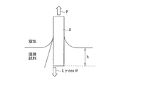
- FIG. 12 is a diagram illustrating the principle of the present technology.
- the contact angle (dynamic contact angle) in a dynamic state in which the interface between a liquid and an object (solid) moves can be measured using, for example, the Wilhelmy method (plate method or vertical plate method).
- the liquid sample touches the surface of the solid sample A the liquid wets the solid sample A.
- surface tension works along the periphery of the solid sample A, and tries to draw the solid sample A into the liquid.
- the force (L ⁇ cos ⁇ ) for pulling the solid sample A into the liquid is represented by the following formula (1), for example.
- the flux 33 crawls on the side surface (surface S3) of the semiconductor substrate 11. It is easy to go up. As a result, the force of pulling the semiconductor device 10 into the flux 33 is increased, and the contact between the bump 12 on the semiconductor device 10 side and the electrode 22 on the mounting substrate 20 side due to its own weight is assisted. Therefore, the connection failure at the time of mounting can be reduced, and the manufacturing yield can be improved.
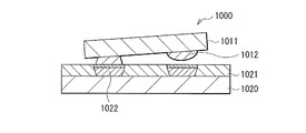
- the flux may crawl on the side surface of the microchip.
- the flux crawls only on a part of the side surface of the semiconductor substrate 1011 as shown in FIG.
- fusion connection occurs only between some solder on the microchip 100 side and some electrodes 1022 embedded in the wiring layer 1021 provided on the mounting substrate 1020, and as shown in FIG.
- a Manhattan phenomenon in which one side of the microchip 1000 rises, and a connection failure such as a rotational displacement of the microchip 1000 as shown in FIG. 11 occurs.
- the plurality of grooves 11X are formed substantially uniformly on at least a pair of opposing side surfaces, for example, the surfaces S3A and S3B and the surfaces 3C and 3D, and more preferably, the side surfaces of the semiconductor substrate 11. (Surface S3) is formed on the entire surface.
- This causes the semiconductor device 10 to sink horizontally into the flux 33. Therefore, the defective connection as described above can be reduced, and the manufacturing yield can be further improved. In addition, the number of steps for repairing the connection failure can be reduced, and the manufacturing cost can be reduced.
- FIG. 13 illustrates a flow of manufacturing steps of the semiconductor device (semiconductor device 10) according to the modified example of the present disclosure.
- the side surface (surface S3) of the semiconductor substrate 11 forming the semiconductor device 10 may have hydrophilicity.
- the semiconductor device 10 can be manufactured as follows, for example.
- the semiconductor substrate 11A provided with the plurality of semiconductor devices 10 is attached to the support substrate 31 via the adhesive layer 32 (step S201).
- the semiconductor substrate 11 is separated and singulated by, for example, dry etching.
- a plurality of grooves 11X are formed on the side surface of the semiconductor substrate 11 (step S202).
- the side surface of the individualized semiconductor device 10 is subjected to a hydrophilic treatment (step S203). Hydrophilization can be performed by, for example, plasma ashing.
- the bumps 12 are formed on the semiconductor substrate 11A by, for example, plating (step S204). The semiconductor device 10 whose side surfaces have been hydrophilized is completed.
- the present disclosure is not limited to the above embodiments and the like, and various modifications can be made.
- the light emitting device LED chip
- the semiconductor device of the present disclosure may be, for example, a sensor device, a light receiving element, or the like.
- an integrated circuit (IC) or the like may be formed.
- the present disclosure may have the following configurations. According to the present technology having the following configuration, since the uneven structure is formed on the side surface of the package substrate on which the semiconductor element is arranged by dry etching, the surface tension on the side surface of the package substrate increases. Therefore, the contact between the semiconductor device and the mounting substrate due to its own weight is assisted, and the manufacturing yield can be improved. Note that the effects described here are not necessarily limited, and may be any effects described in the present disclosure. (1) A semiconductor substrate having one surface and the other surface facing each other and one side of which is 50 ⁇ m or more and 500 ⁇ m or less; One or more bumps provided on the other surface, And a concavo-convex structure formed on a side surface of the semiconductor substrate.
- the semiconductor substrate has a plurality of grooves extending in the normal direction to the one surface and the other surface as the uneven structure.
- the plurality of grooves are formed substantially uniformly on at least a pair of opposing side surfaces.
- the plurality of grooves have a substantially semicircular shape, a substantially rectangular shape, or a substantially triangular cross-sectional shape with respect to the horizontal direction of the one surface and the other surface.
- the semiconductor device is A semiconductor substrate having one surface and the other surface facing each other and one side of which is 50 ⁇ m or more and 500 ⁇ m or less; One or more bumps provided on the other surface, A semiconductor device having a concavo-convex structure formed on a side surface of the semiconductor substrate. (10) Further having a sealing member on the mounting substrate, The semiconductor device according to (9), wherein the semiconductor device is sealed by the sealing member.
- the semiconductor device is A semiconductor substrate having one surface and the other surface facing each other; One or more bumps provided on the other surface, A semiconductor device having a concavo-convex structure formed on a side surface of the semiconductor substrate by dry etching.
Landscapes
- Wire Bonding (AREA)
- Dicing (AREA)
Abstract
本開示の一実施形態の第1の半導体デバイスは、対向する一の面および他の面を有する一辺が50μm以上500μm以下の半導体基板と、他の面に設けられた1または複数のバンプと、半導体基板の側面に形成された凹凸構造とを備える。
Description
本開示は、バンプを用いて基板上に実装される半導体デバイスおよびこれを備えた半導体装置に関する。
フラックスリフローによるチップ実装では、チップは自重によりフラックスに沈み、チップ側の半田と、基板側のアンダーバンプメタル(UBM)とが接触する。その状態で加熱することでチップ側の半田と、基板側のUBMとが溶融接続される。例えば、特許文献1では、チップの端面に凹凸パターンを設けることで樹脂フィレットとの接着強度を向上させてチップと基板との接着強度を高めた半導体装置が開示されている。
ところで、微細なチップをフラックスリフローによって実装する場合、接続不良が起こりやすく、製造歩留まりが低下する。このため、製造歩留まりの向上が求められている。
製造歩留まりを向上させることが可能な半導体デバイスおよび半導体装置を提供することが望ましい。
本開示の一実施形態の第1の半導体デバイスは、対向する一の面および他の面を有する一辺が50μm以上500μm以下の半導体基板と、他の面に設けられた1または複数のバンプと、半導体基板の側面に形成された凹凸構造とを備えたものである。
本開示の一実施形態の第1の半導体装置は、実装基板上に複数の半導体デバイスが実装されたものであり、複数の半導体デバイスとして、上記一実施形態の第1の半導体デバイスを備えたものである。
本開示の一実施形態の第2の半導体デバイスは、対向する一の面および他の面を有する半導体基板と、他の面に設けられた1または複数のバンプと、半導体基板の側面にドライエッチングによって形成された凹凸構造とを備えたものである。
本開示の一実施形態の第2の半導体装置は、実装基板上に複数の半導体デバイスが実装されたものであり、複数の半導体デバイスとして、上記一実施形態の第2の半導体デバイスを備えたものである。
本開示の一実施形態の第1の半導体デバイスおよび一実施形態の第1の半導体装置ならびに一実施形態の第2の半導体デバイスおよび一実施形態の第2の半導体装置では、半導体素子が配設された半導体基板の側面にドライエッチングによって凹凸構造を形成した。これにより、半導体基板の側面の表面張力が大きくなる。
以下、本開示における一実施形態について、図面を参照して詳細に説明する。以下の説明は本開示の一具体例であって、本開示は以下の態様に限定されるものではない。また、本開示は、各図に示す各構成要素の配置や寸法、寸法比等についても、それらに限定されるものではない。なお、説明する順序は、下記の通りである。
1.実施の形態(チップ基板の側面に溝を設けた半導体デバイスの例)
1-1.半導体デバイスの構成
1-2.半導体デバイスの製造方法
1-3.半導体装置の構成
1-4.作用・効果
2.変形例(さらにチップ基板の側面を親水化処理した半導体デバイスの例)
1.実施の形態(チップ基板の側面に溝を設けた半導体デバイスの例)
1-1.半導体デバイスの構成
1-2.半導体デバイスの製造方法
1-3.半導体装置の構成
1-4.作用・効果
2.変形例(さらにチップ基板の側面を親水化処理した半導体デバイスの例)
<1.実施の形態>
(1-1.半導体デバイスの構成)
図1は、本開示の一実施の形態に係る半導体デバイス(半導体デバイス10)の断面構成を表したものである。図2は、図1に示した半導体デバイス10の平面構成を表したものである。なお、図1では、例えば、図2に示したI-I線における断面を表している。半導体デバイス10は、対向する一の面(面S1)および他の面(面S2)を有する半導体基板11の面S2に1または複数のバンプ12を有し、さらに、半導体基板11の側面(面S3)に凹凸構造として複数の溝11Xが形成されたものである。なお、図1および図2は半導体デバイス10の構成を模式的に表したものであり、実際の寸法、形状とは異なる場合がある。
(1-1.半導体デバイスの構成)
図1は、本開示の一実施の形態に係る半導体デバイス(半導体デバイス10)の断面構成を表したものである。図2は、図1に示した半導体デバイス10の平面構成を表したものである。なお、図1では、例えば、図2に示したI-I線における断面を表している。半導体デバイス10は、対向する一の面(面S1)および他の面(面S2)を有する半導体基板11の面S2に1または複数のバンプ12を有し、さらに、半導体基板11の側面(面S3)に凹凸構造として複数の溝11Xが形成されたものである。なお、図1および図2は半導体デバイス10の構成を模式的に表したものであり、実際の寸法、形状とは異なる場合がある。
半導体デバイス10は、例えば一辺が50μm以上500μm以下、より具体的には、一辺が80μm以上200μmの半導体チップである。半導体デバイス10は、例えば、いわゆるLED(Light Emitting Diode)ディスプレイと呼ばれる画像表示装置の表示画素として好適に用いられるLEDチップである。LEDチップは、本開示の「半導体デバイス」の一具体例に相当する。半導体デバイス10は、上記のように、半導体基板11の側面(面S3)に複数の溝11Xが設けられている。
複数の溝11Xは、詳細は後述するが、フラックスリフローによる実装基板20への実装時におけるバンプ12と実装基板20側の電極22との接触を補助するためのものである(例えば、図5E参照)。複数の溝11Xは、例えば、図1に示したように、半導体基板11の側面(面S3)に複数設けられている。これにより、半導体デバイス10の表面積が増加し、フラックスリフロー時における半導体デバイス10のバンプ12と実装基板20側の実装用の電極22との接触が容易となる。なお、電極22上には、例えば金(Au)めっきからなる酸化防止膜23が設けられている。
複数の溝11Xは、例えば、図1に示したように、対向する面S1および面S2に対して法線方向(例えば、Y軸方向)に、互いに平行に延伸している。複数の溝11Xの面S1および面S2に対して水平方向(例えば、XZ平面方向)の断面は、例えば、図2に示したように、略半円状の形状を有するがこれに限らない。複数の溝11Xは、上記のように、半導体デバイス10の表面積を増加させるためのものであるため、例えば、図3Aに示したような略矩形状や、図3Bに示したような略三角状の断面形状としてもよい。更に、図1等ではY軸方向に直線上に延伸する複数の溝11Xの例を示したが、複数の溝11Xの延伸方向はこれに限らない。例えば、複数の溝11Xは、図3Cに示したように、Y軸方向に蛇行する溝としてもよい。また、複数の溝11Xは、図3Dに示したように、対向する面S1および面S2に対して水平方向(例えば、X軸方向またはZ軸方向)に延伸する溝としてもよい。更に、複数の溝11Xは、図3Eに示したように、例えば格子状に形成してもよい。
複数の溝11Xは、半導体基板11の側面(面S3)全体に形成されていることが好ましい。また、複数の溝11Xは、対向する一対の側面、例えば面S3Aと面S3Bおよび面3Cと面3Dにおいて略均一に形成されていることが好ましい。これにより、対向する各側面、例えば面S3Aとフラックス33との間で発生する表面張力と、面S3Bとフラックス33との間で発生する表面張力とが釣り合い、フラックスリフロー時に、半導体デバイス10がフラックス33に、水平に沈み込むようになる。
(1-2.半導体デバイスの製造方法)
本実施の形態の半導体デバイス10は、例えば次のようにして製造することができる。図4は、半導体デバイス10の製造工程の流れを表したものである。図5A~図5Fは、半導体デバイス10の製造工程の一例を表したものである。
本実施の形態の半導体デバイス10は、例えば次のようにして製造することができる。図4は、半導体デバイス10の製造工程の流れを表したものである。図5A~図5Fは、半導体デバイス10の製造工程の一例を表したものである。
まず、図5Aに示したように、例えば支持基板31上に、接着層32を介して複数の半導体デバイス10が設けられた半導体基板11Aを貼り合わせる(ステップS101)。次に、図5Bに示したように、半導体基板11A上に、例えばめっきによってバンプ12を形成する(ステップS102)。続いて、図5Cに示したように、ドライエッチングにより半導体基板11を分離、個片化する。同時に、半導体基板11の側面に複数の溝11Xを形成する(ステップS103)。これにより、図1に示した半導体デバイス10が完成する。その後、図5D~図5Fに示したように、半導体デバイス10を実装基板20上に実装する(ステップS104)。
実装基板20への半導体デバイス10の実装は、例えば、以下のようにして行う。まず、実装基板20を用意する。実装基板20上には、表面に酸化防止膜23が積層された電極22を有する配線層21が設けられている。この実装基板20上に、図5Dに示したように、フラックス33を、例えば、半導体デバイス10のバンプ12が浸かる程度の厚みで塗布したのち、フラックス33上に半導体デバイス10を置く。このとき、フラックス33は、半導体基板11の側面(面S3)に形成された複数の溝11Xによって、図5Eに示したように、半導体基板11の側面(面S3)を這い上がる。同時に、半導体基板11は、表面張力によってフラックス33中に引き込まれ、バンプ12と電極22とが接触する。その後、加熱することにより、図5Fに示したように、バンプ12が溶融し、電極22と接合される。その後、フラックス33は、洗浄工程を経て除去される。以上により、実装基板20上への半導体デバイス10の実装が完了する。
なお、半導体デバイス10の側面(具体的には、半導体基板11の側面(面S3))には、必要に応じて実装後に絶縁膜を形成してもよい。絶縁膜は、例えば、スパッタ、インクジェット印刷またはスクリーン印刷等を用いて成膜することができる。また、半導体デバイス10の側面に絶縁膜を形成する場合には、側面をテーパ状に加工するようにしてもよい。これにより、半導体デバイス10の側面に絶縁膜を容易に成膜することが可能となる。
(1-3.半導体装置の構成)
図6は、本開示の半導体装置の一具体例としての表示装置1の概略構成の一例を斜視的に表したものである。表示装置1は、いわゆるLEDディスプレイと呼ばれるものであり、表示画素としてLEDが用いられたものである。表示装置1は、例えば図6に示したように、表示パネル110と、表示パネル110を駆動する駆動回路(図示せず)とを備えている。
図6は、本開示の半導体装置の一具体例としての表示装置1の概略構成の一例を斜視的に表したものである。表示装置1は、いわゆるLEDディスプレイと呼ばれるものであり、表示画素としてLEDが用いられたものである。表示装置1は、例えば図6に示したように、表示パネル110と、表示パネル110を駆動する駆動回路(図示せず)とを備えている。
表示パネル110は、実装基板120と、透明基板130とを互いに重ね合わせたものである。透明基板130の表面が映像表示面となっており、中央部分に表示領域1Aを有し、その周囲に、非表示領域であるフレーム領域1Bを有している。
図7は、実装基板120の透明基板130側の表面のうち表示領域1Aに対応する領域のレイアウトの一例を表したものである。実装基板120の表面のうち表示領域1Aに対応する領域には、例えば図7に示したように、複数のデータ配線221が所定の方向に延在して形成されており、かつ所定のピッチで並列配置されている。実装基板120の表面のうち表示領域1Aに対応する領域には、さらに、例えば、複数のスキャン配線222がデータ配線221と交差(例えば、直交)する方向に延在して形成されており、且つ、所定のピッチで並列配置されている。データ配線221およびスキャン配線222は、例えば、Cu(銅)等の導電性材料からなる。
スキャン配線222は、例えば、最表層に形成されており、例えば、基材表面に形成された絶縁層(図示せず)上に形成されている。なお、実装基板220の基材は、例えば、ガラス基板、または樹脂基板等からなり、基材上の絶縁層は、例えば、SiNx、SiOx、またはAlxOyからなる。一方、データ配線221は、スキャン配線222を含む最表層とは異なる層(例えば、最表層よりも下の層)内に形成されており、例えば、基材上の絶縁層内に形成されている。絶縁層の表面上には、スキャン配線222の他に、例えば、必要に応じてブラックが設けられている。ブラックは、コントラストを高めるためのものであり、光吸収性の材料によって構成されている。ブラックは、例えば、絶縁層の表面のうち少なくとも後述のパッド電極221B,222Bの非形成領域に形成されている。なお、ブラックは、必要に応じて省略することも可能である。
データ配線221とスキャン配線222との交差部分の近傍が表示画素223となっており、複数の表示画素223が表示領域1A内においてマトリクス状に配置されている。各表示画素223には、複数の発光デバイスを含む発光ユニットが実装されている。なお、図7では、一つの表示画素223は、R,G,Bに対応する3つの発光デバイスによって構成されている。
図8は、図6に示した実装基板120の断面構成を模式的に表したものである。実装基板120上には、上記発光デバイスとして、例えば3つの半導体デバイス10R,10G,10Bが実装されている。
半導体デバイス10R,10G,10Bは、互いに所定の間隙を介して一列に配置されている。互いに隣り合う半導体デバイス10R,10G,10Bの隙間は、例えば、各半導体デバイス10R,10G,10Bのサイズと同等か、それよりも狭くなっていている。なお、上記隙間は、場合によっては各半導体デバイス10のサイズよりも大きくなっていてもよい。
発光デバイスとして用いられる半導体デバイス10R,10G,10Bは、互いに異なる波長の光を発するようになっている。例えば、半導体デバイス10Rは赤色帯の光(Lr)を、半導体デバイス10Gは緑色帯の光(Lg)を、半導体デバイス10Bは青色帯の光(Lb)を発するようになっている。半導体デバイス10R,10G,10Bは、例えば封止樹脂140によって1パッケージに封止され、実装基板120上に実装される形態をとってもよい。この封止樹脂140が、本開示の「封止部材」の一具体例に相当する。
(1-4.作用・効果)
前述したように、フラックスリフローによるチップ実装では、チップは自重によりフラックスに沈み、チップ側の半田と、基板側のUBMとが接触する。チップ側の半田と、基板側のUBMとが接触した状態で加熱することで溶融接続される。
前述したように、フラックスリフローによるチップ実装では、チップは自重によりフラックスに沈み、チップ側の半田と、基板側のUBMとが接触する。チップ側の半田と、基板側のUBMとが接触した状態で加熱することで溶融接続される。
ところが、例えば、一辺が500μm以下に微細化されたチップ(以下、マイクロチップと称する)をフラックスリフローによって実装しようとした場合、マイクロチップは上記のように自重によってフラックスに沈まず、浮いてしまう。この状態では、マイクロチップ側の半田と、基板側のUBMとの接触がなされず、接続不良が発生し、製造歩留まりが低下する。
これに対して本実施の形態では、半導体デバイス10の側面の表面張力を制御した。具体的には、半導体デバイス10の側面(具体的には、半導体基板11の側面(面S3))に凹凸構造として複数の溝11Xを形成した。
図12は、本技術の原理を説明する図である。液体と物体(固体)との界面が動く動的な状態における接触角(動的接触角)は、例えば、Wilhelmy法(プレート法または垂直板法)を用いて測定することができる。液体試料が固体試料Aの表面に触れると、液体が固体試料Aに対してぬれ上がる。そのとき、固体試料Aの周囲に沿って表面張力が働き、固体試料Aを液中に引き込もうとする。この固体試料Aを液中に引き込もうとする力(Lγcosθ)は、例えば、下記式(1)のように表される。下記式(1)から、固体試料の周囲長(L)が大きくなるほど固体試料Aを液中に引き込もうとする力(Lγcosθ)が大きくなることがわかる。
(数式)F=Lγcosθ-Shρg・・・・・・(1)
θ:固体試料と液体試料との接触角
F:測定力(固体試料にはたらく力)
S:固体試料の断面積
h:固体試料の浸漬距離
ρ:液体試料の密度
L:固体試料の周囲長
γ:表面張力
(数式)F=Lγcosθ-Shρg・・・・・・(1)
θ:固体試料と液体試料との接触角
F:測定力(固体試料にはたらく力)
S:固体試料の断面積
h:固体試料の浸漬距離
ρ:液体試料の密度
L:固体試料の周囲長
γ:表面張力
以上のように、本実施の形態の半導体デバイス10では、半導体基板11の側面(面S3)に複数の溝11Xを設けるようにしたので、フラックス33が半導体基板11の側面(面S3)に這い上がりやすくなる。これにより、半導体デバイス10をフラックス33中に引き込もうとする力が大きくなり、自重による半導体デバイス10側のバンプ12と、実装基板20側の電極22との接触が補助される。よって、実装時の接続不良が低減され、製造歩留まりを向上させることが可能となる。
また、フラックスは、マイクロチップの側面を這い上がることがあるが、例えば、マイクロチップ1000では、図9に示したように、フラックスが半導体基板1011の側面の一部にのみ這い上がったりする。その結果、マイクロチップ100側の一部の半田と実装基板1020上に設けられた配線層1021に埋設された一部の電極1022との間でのみ溶融接続が起こり、図10に示したようにマイクロチップ1000の片側が立ち上がるマンハッタン現象や、図11に示したようなマイクロチップ1000の回転ズレ等の接続不良が発生する。
これに対して本実施の形態では、複数の溝11Xを少なくとも対向する一対の側面、例えば面S3Aと面S3Bおよび面3Cと面3Dにおいて略均一に形成し、より好ましくは、半導体基板11の側面(面S3)全体に形成するようにした。これにより、半導体デバイス10がフラックス33に、水平に沈み込むようになる。よって、上述したような接続不良が低減され、製造歩留まりをさらに向上させることが可能となる。加えて、接続不良を修復する工程が削減されるようになり、製造コストを低減することが可能となる。
<2.変形例>
図13は、本開示の変形例に係る半導体デバイス(半導体デバイス10)の製造工程の流れを表したものである。半導体デバイス10を構成する半導体基板11の側面(面S3)は、親水性を有していてもよい。その場合、半導体デバイス10は、例えば次のようにして製造することができる。
図13は、本開示の変形例に係る半導体デバイス(半導体デバイス10)の製造工程の流れを表したものである。半導体デバイス10を構成する半導体基板11の側面(面S3)は、親水性を有していてもよい。その場合、半導体デバイス10は、例えば次のようにして製造することができる。
まず、上記実施の形態と同様に、例えば支持基板31上に、接着層32を介して複数の半導体デバイス10が設けられた半導体基板11Aを貼り合わせる(ステップS201)。次に、例えばドライエッチングにより半導体基板11を分離、個片化する。同時に、半導体基板11の側面に複数の溝11Xを形成する(ステップS202)。続いて、個片化された半導体デバイス10の側面に親水化処理を施す(ステップS203)。親水化は、例えばプラズマアッシング等で行うことができる。次に、半導体基板11A上に、例えばめっきによってバンプ12を形成する(ステップS204)。側面が親水化処理された半導体デバイス10が完成する。
このように、半導体基板11の側面を親水化処理することにより、実装時にフラックス33との表面張力が効果的に発生するようになり、半導体デバイス10側のバンプ12と、実装基板20側の電極22との接続不良をさらに低減することが可能となる。即ち、製造歩留まりをさらに向上させることが可能となる。
以上、実施の形態および変形例を挙げて説明したが、本開示内容は上記実施の形態等に限定されるものではなく、種々変形が可能である。例えば、上記実施の形態では、半導体デバイス10の一具体例として発光デバイス(LEDチップ)を挙げたが、本開示の半導体デバイスは、例えば、センサデバイスや受光素子等でもよい。また、例えば集積回路(IC)等が形成されていてもよい。
なお、本開示は、以下のような構成も可能である。以下の構成の本技術によれば、半導体素子が配設されたパッケージ基板の側面にドライエッチングによって凹凸構造を形成したので、パッケージ基板の側面の表面張力が大きくなる。よって、半導体デバイスと実装基板との自重による接触が補助され、製造歩留まりを向上させることが可能となる。なお、ここに記載された効果は必ずしも限定されるものではなく、本開示中に記載されたいずれの効果であってもよい。
(1)
対向する一の面および他の面を有する一辺が50μm以上500μm以下の半導体基板と、
前記他の面に設けられた1または複数のバンプと、
前記半導体基板の側面に形成された凹凸構造と
を備えた半導体デバイス。
(2)
前記凹凸構造は、前記半導体基板の前記側面全体に形成されている、前記(1)に記載の半導体デバイス。
(3)
前記半導体基板は、前記凹凸構造として前記一の面および前記他の面に対して法線方向に延伸する複数の溝を有する、前記(1)または(2)に記載の半導体デバイス。
(4)
前記複数の溝は、少なくとも対向する一対の側面において略均一に形成されている、前記(3)に記載の半導体デバイス。
(5)
前記複数の溝は、前記一の面および前記他の面の水平方向に対して、略半円状、略矩形状、略三角状の断面形状を有する、前記(3)または(4)に記載の半導体デバイス。
(6)
前記半導体基板の前記側面は親水性を有する、前記(1)乃至(5)のうちのいずれかに記載の半導体デバイス。
(7)
前記半導体基板の一辺は80μm以上200μm以下である、前記(1)乃至(6)のうちのいずれかに記載の半導体デバイス。
(8)
対向する一の面および他の面を有する半導体基板と、
前記他の面に設けられた1または複数のバンプと、
前記半導体基板の側面にドライエッチングによって形成された凹凸構造と
を備えた半導体デバイス。
(9)
実装基板上に実装された複数の半導体デバイスを備え、
前記半導体デバイスは、
対向する一の面および他の面を有する一辺が50μm以上500μm以下の半導体基板と、
前記他の面に設けられた1または複数のバンプと、
前記半導体基板の側面に形成された凹凸構造と
を有する半導体装置。
(10)
前記実装基板上に封止部材をさらに有し、
前記半導体デバイスは、前記封止部材によって封止されている、前記(9)に記載の半導体装置。
(11)
実装基板上に実装された複数の半導体デバイスを備え、
前記半導体デバイスは、
対向する一の面および他の面を有する半導体基板と、
前記他の面に設けられた1または複数のバンプと、
前記半導体基板の側面にドライエッチングによって形成された凹凸構造と
を有する半導体装置。
(1)
対向する一の面および他の面を有する一辺が50μm以上500μm以下の半導体基板と、
前記他の面に設けられた1または複数のバンプと、
前記半導体基板の側面に形成された凹凸構造と
を備えた半導体デバイス。
(2)
前記凹凸構造は、前記半導体基板の前記側面全体に形成されている、前記(1)に記載の半導体デバイス。
(3)
前記半導体基板は、前記凹凸構造として前記一の面および前記他の面に対して法線方向に延伸する複数の溝を有する、前記(1)または(2)に記載の半導体デバイス。
(4)
前記複数の溝は、少なくとも対向する一対の側面において略均一に形成されている、前記(3)に記載の半導体デバイス。
(5)
前記複数の溝は、前記一の面および前記他の面の水平方向に対して、略半円状、略矩形状、略三角状の断面形状を有する、前記(3)または(4)に記載の半導体デバイス。
(6)
前記半導体基板の前記側面は親水性を有する、前記(1)乃至(5)のうちのいずれかに記載の半導体デバイス。
(7)
前記半導体基板の一辺は80μm以上200μm以下である、前記(1)乃至(6)のうちのいずれかに記載の半導体デバイス。
(8)
対向する一の面および他の面を有する半導体基板と、
前記他の面に設けられた1または複数のバンプと、
前記半導体基板の側面にドライエッチングによって形成された凹凸構造と
を備えた半導体デバイス。
(9)
実装基板上に実装された複数の半導体デバイスを備え、
前記半導体デバイスは、
対向する一の面および他の面を有する一辺が50μm以上500μm以下の半導体基板と、
前記他の面に設けられた1または複数のバンプと、
前記半導体基板の側面に形成された凹凸構造と
を有する半導体装置。
(10)
前記実装基板上に封止部材をさらに有し、
前記半導体デバイスは、前記封止部材によって封止されている、前記(9)に記載の半導体装置。
(11)
実装基板上に実装された複数の半導体デバイスを備え、
前記半導体デバイスは、
対向する一の面および他の面を有する半導体基板と、
前記他の面に設けられた1または複数のバンプと、
前記半導体基板の側面にドライエッチングによって形成された凹凸構造と
を有する半導体装置。
本出願は、日本国特許庁において2019年2月19日に出願された日本特許出願番号2019-027481号を基礎として優先権を主張するものであり、この出願の全ての内容を参照によって本出願に援用する。
当業者であれば、設計上の要件や他の要因に応じて、種々の修正、コンビネーション、サブコンビネーション、および変更を想到し得るが、それらは添付の請求の範囲やその均等物の範囲に含まれるものであることが理解される。
Claims (11)
- 対向する一の面および他の面を有する一辺が50μm以上500μm以下の半導体基板と、
前記他の面に設けられた1または複数のバンプと、
前記半導体基板の側面に形成された凹凸構造と
を備えた半導体デバイス。 - 前記凹凸構造は、前記半導体基板の前記側面全体に形成されている、請求項1に記載の半導体デバイス。
- 前記半導体基板は、前記凹凸構造として前記一の面および前記他の面に対して法線方向に延伸する複数の溝を有する、請求項1に記載の半導体デバイス。
- 前記複数の溝は、少なくとも対向する一対の側面において略均一に形成されている、請求項3に記載の半導体デバイス。
- 前記複数の溝は、前記一の面および前記他の面の水平方向に対して、略半円状、略矩形状、略三角状の断面形状を有する、請求項3に記載の半導体デバイス。
- 前記半導体基板の前記側面は親水性を有する、請求項1に記載の半導体デバイス。
- 前記半導体基板の一辺は80μm以上200μm以下である、請求項1に記載の半導体デバイス。
- 対向する一の面および他の面を有する半導体基板と、
前記他の面に設けられた1または複数のバンプと、
前記半導体基板の側面にドライエッチングによって形成された凹凸構造と
を備えた半導体デバイス。 - 実装基板上に実装された複数の半導体デバイスを備え、
前記半導体デバイスは、
対向する一の面および他の面を有する一辺が50μm以上500μm以下の半導体基板と、
前記他の面に設けられた1または複数のバンプと、
前記半導体基板の側面に形成された凹凸構造と
を有する半導体装置。 - 前記実装基板上に封止部材をさらに有し、
前記半導体デバイスは、前記封止部材によって封止されている、請求項9に記載の半導体装置。 - 実装基板上に実装された複数の半導体デバイスを備え、
前記半導体デバイスは、
対向する一の面および他の面を有する半導体基板と、
前記他の面に設けられた1または複数のバンプと、
前記半導体基板の側面にドライエッチングによって形成された凹凸構造と
を有する半導体装置。
Priority Applications (1)
| Application Number | Priority Date | Filing Date | Title |
|---|---|---|---|
| US17/430,392 US12068434B2 (en) | 2019-02-19 | 2020-02-07 | Semiconductor device and semiconductor unit |
Applications Claiming Priority (2)
| Application Number | Priority Date | Filing Date | Title |
|---|---|---|---|
| JP2019-027481 | 2019-02-19 | ||
| JP2019027481A JP2020136462A (ja) | 2019-02-19 | 2019-02-19 | 半導体デバイスおよび半導体装置 |
Publications (1)
| Publication Number | Publication Date |
|---|---|
| WO2020170855A1 true WO2020170855A1 (ja) | 2020-08-27 |
Family
ID=72144785
Family Applications (1)
| Application Number | Title | Priority Date | Filing Date |
|---|---|---|---|
| PCT/JP2020/004789 Ceased WO2020170855A1 (ja) | 2019-02-19 | 2020-02-07 | 半導体デバイスおよび半導体装置 |
Country Status (3)
| Country | Link |
|---|---|
| US (1) | US12068434B2 (ja) |
| JP (1) | JP2020136462A (ja) |
| WO (1) | WO2020170855A1 (ja) |
Citations (1)
| Publication number | Priority date | Publication date | Assignee | Title |
|---|---|---|---|---|
| JP2002118208A (ja) * | 2000-10-11 | 2002-04-19 | Ricoh Co Ltd | 半導体部品の封止構造および半導体部品の封止方法 |
Family Cites Families (1)
| Publication number | Priority date | Publication date | Assignee | Title |
|---|---|---|---|---|
| JP4495916B2 (ja) | 2003-03-31 | 2010-07-07 | 富士通マイクロエレクトロニクス株式会社 | 半導体チップの製造方法 |
-
2019
- 2019-02-19 JP JP2019027481A patent/JP2020136462A/ja active Pending
-
2020
- 2020-02-07 WO PCT/JP2020/004789 patent/WO2020170855A1/ja not_active Ceased
- 2020-02-07 US US17/430,392 patent/US12068434B2/en active Active
Patent Citations (1)
| Publication number | Priority date | Publication date | Assignee | Title |
|---|---|---|---|---|
| JP2002118208A (ja) * | 2000-10-11 | 2002-04-19 | Ricoh Co Ltd | 半導体部品の封止構造および半導体部品の封止方法 |
Also Published As
| Publication number | Publication date |
|---|---|
| JP2020136462A (ja) | 2020-08-31 |
| US20220149235A1 (en) | 2022-05-12 |
| US12068434B2 (en) | 2024-08-20 |
Similar Documents
| Publication | Publication Date | Title |
|---|---|---|
| JP4870584B2 (ja) | 半導体装置 | |
| JP2014013818A (ja) | デバイスおよび電子装置 | |
| KR102322539B1 (ko) | 반도체 패키지 및 이를 포함하는 디스플레이 장치 | |
| CN101897175B (zh) | 焊接连接可靠性改进的可回焊相机模块 | |
| JP4719009B2 (ja) | 基板および半導体装置 | |
| JP2013541858A (ja) | ノーフローアンダーフィル | |
| JP2012059832A5 (ja) | ||
| JP6423685B2 (ja) | 電子部品、モジュール及びカメラ | |
| JP2008270650A (ja) | 光学デバイスおよびその製造方法。 | |
| CN102163581B (zh) | 半导体模块 | |
| JP5290215B2 (ja) | 半導体装置、半導体パッケージ、インタポーザ、及びインタポーザの製造方法 | |
| JP2020004926A (ja) | 配線基板及び配線基板の製造方法 | |
| TWI615934B (zh) | 半導體裝置、顯示面板總成、半導體結構 | |
| TWI559464B (zh) | 封裝模組及其基板結構 | |
| KR102378493B1 (ko) | 패키지 기판용 필름, 반도체 패키지, 디스플레이 장치 및 이들의 제조 방법 | |
| TWI395280B (zh) | 用於晶圓級半導體測試之測試座及測試板 | |
| WO2020170855A1 (ja) | 半導体デバイスおよび半導体装置 | |
| US9815133B2 (en) | Method for producing a module | |
| JP4976673B2 (ja) | 半導体装置、基板及び半導体装置の製造方法 | |
| CN116682834A (zh) | 图像传感器芯片封装结构及图像获取装置 | |
| JP5489860B2 (ja) | 積層型半導体モジュール | |
| KR20200080166A (ko) | 표시 장치 및 표시 장치의 제조 방법 | |
| TW201306197A (zh) | 以金屬柱銲接為晶片連接之半導體封裝構造 | |
| JP2005121757A (ja) | 基板接続構造、電子部品、液晶表示装置および電子部品の製造方法 | |
| JP4913372B2 (ja) | 半導体装置 |
Legal Events
| Date | Code | Title | Description |
|---|---|---|---|
| 121 | Ep: the epo has been informed by wipo that ep was designated in this application |
Ref document number: 20759008 Country of ref document: EP Kind code of ref document: A1 |
|
| NENP | Non-entry into the national phase |
Ref country code: DE |
|
| 122 | Ep: pct application non-entry in european phase |
Ref document number: 20759008 Country of ref document: EP Kind code of ref document: A1 |