WO2020170521A1 - 切削加工された粘着剤層付光学積層体の製造方法 - Google Patents
切削加工された粘着剤層付光学積層体の製造方法 Download PDFInfo
- Publication number
- WO2020170521A1 WO2020170521A1 PCT/JP2019/044859 JP2019044859W WO2020170521A1 WO 2020170521 A1 WO2020170521 A1 WO 2020170521A1 JP 2019044859 W JP2019044859 W JP 2019044859W WO 2020170521 A1 WO2020170521 A1 WO 2020170521A1
- Authority
- WO
- WIPO (PCT)
- Prior art keywords
- adhesive layer
- sensitive adhesive
- pressure
- manufacturing
- optical
- Prior art date
- Legal status (The legal status is an assumption and is not a legal conclusion. Google has not performed a legal analysis and makes no representation as to the accuracy of the status listed.)
- Ceased
Links
Images


Classifications
-
- G—PHYSICS
- G02—OPTICS
- G02B—OPTICAL ELEMENTS, SYSTEMS OR APPARATUS
- G02B5/00—Optical elements other than lenses
- G02B5/30—Polarising elements
-
- B—PERFORMING OPERATIONS; TRANSPORTING
- B23—MACHINE TOOLS; METAL-WORKING NOT OTHERWISE PROVIDED FOR
- B23C—MILLING
- B23C3/00—Milling particular work; Special milling operations; Machines therefor
- B23C3/12—Trimming or finishing edges, e.g. deburring welded corners
-
- B—PERFORMING OPERATIONS; TRANSPORTING
- B23—MACHINE TOOLS; METAL-WORKING NOT OTHERWISE PROVIDED FOR
- B23C—MILLING
- B23C3/00—Milling particular work; Special milling operations; Machines therefor
- B23C3/13—Surface milling of plates, sheets or strips
-
- B—PERFORMING OPERATIONS; TRANSPORTING
- B23—MACHINE TOOLS; METAL-WORKING NOT OTHERWISE PROVIDED FOR
- B23C—MILLING
- B23C3/00—Milling particular work; Special milling operations; Machines therefor
- B23C3/16—Working surfaces curved in two directions
-
- B—PERFORMING OPERATIONS; TRANSPORTING
- B23—MACHINE TOOLS; METAL-WORKING NOT OTHERWISE PROVIDED FOR
- B23C—MILLING
- B23C5/00—Milling-cutters
- B23C5/02—Milling-cutters characterised by the shape of the cutter
- B23C5/10—Shank-type cutters, i.e. with an integral shaft
-
- B—PERFORMING OPERATIONS; TRANSPORTING
- B23—MACHINE TOOLS; METAL-WORKING NOT OTHERWISE PROVIDED FOR
- B23C—MILLING
- B23C5/00—Milling-cutters
- B23C5/02—Milling-cutters characterised by the shape of the cutter
- B23C5/12—Cutters specially designed for producing particular profiles
-
- G—PHYSICS
- G02—OPTICS
- G02B—OPTICAL ELEMENTS, SYSTEMS OR APPARATUS
- G02B5/00—Optical elements other than lenses
- G02B5/30—Polarising elements
- G02B5/3025—Polarisers, i.e. arrangements capable of producing a definite output polarisation state from an unpolarised input state
- G02B5/3033—Polarisers, i.e. arrangements capable of producing a definite output polarisation state from an unpolarised input state in the form of a thin sheet or foil, e.g. Polaroid
- G02B5/3041—Polarisers, i.e. arrangements capable of producing a definite output polarisation state from an unpolarised input state in the form of a thin sheet or foil, e.g. Polaroid comprising multiple thin layers, e.g. multilayer stacks
Definitions
- the present invention relates to a method for producing a cut optical laminate with an adhesive layer.
- Image display devices such as mobile phones and notebook personal computers use various optical laminates (for example, polarizing plates) to realize image display and/or enhance the performance of the image display. ..
- an adhesive layer is provided as the outermost layer in the optical layered body so that the optical layered body can be attached to the image display cell.
- a separator is detachably and temporarily attached to the pressure-sensitive adhesive layer to protect the pressure-sensitive adhesive layer until actual use.
- a surface protective film is typically detachably and temporarily attached to the side opposite to the pressure-sensitive adhesive layer of the optical laminate.
- the surface protective film is required to have easy peelability (hereinafter, may be simply referred to as peelability).
- peelability the surface protective film is required to have easy peelability (hereinafter, may be simply referred to as peelability).
- the present invention has been made in order to solve such a problem, its main purpose is to suppress the peeling failure of the surface protective film, to produce a machined pressure-sensitive adhesive layer-attached optical laminate easily and inexpensively To provide a possible method.
- the method for producing a machined pressure-sensitive adhesive layer-carrying optical laminate of the present invention comprises forming a work by laminating a plurality of pressure-sensitive adhesive layer-carrying optical laminates, and using an end mill having a twisting blade, Cutting the outer peripheral surface.
- the optical layered body with a pressure-sensitive adhesive layer comprises an optical film, a pressure-sensitive adhesive layer arranged on one side of the optical film, a separator releasably temporarily attached to the pressure-sensitive adhesive layer, and another optical film. And a surface protection film that is detachably temporarily attached to one side.
- the method for producing an optical layered body with a pressure-sensitive adhesive layer of the present invention comprises stacking a plurality of optical layered bodies with a pressure-sensitive adhesive layer to form a work; and cutting the outer peripheral surface of the work using an end mill having a twisted blade.
- the pressure-sensitive adhesive layer-attached optical laminate is an optical film, a pressure-sensitive adhesive layer arranged on one side of the optical film, a separator that is detachably temporarily attached to the pressure-sensitive adhesive layer, and the other side of the optical film. And a surface protection film that is detachably temporarily attached.
- the work is formed by stacking the optical layered body with the pressure-sensitive adhesive layer such that the separator is positioned in the discharge direction of the cutting dust of the end mill.
- the specific configuration of the pressure-sensitive adhesive layer-carrying optical laminate that can be used in the method for producing the pressure-sensitive adhesive layer-carrying optical laminate of the present invention will be described, and then the pressure-sensitive adhesive layer-carrying optical laminate of the present invention will be described. The manufacturing method will be described.
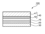
- FIG. 1 is a schematic cross-sectional view illustrating an example of an optical laminate with an adhesive layer that can be used in the manufacturing method of the present invention.
- the optical layered body with a pressure-sensitive adhesive layer 100 of the illustrated example includes an optical film 10, a pressure-sensitive adhesive layer 20 arranged on one side of the optical film 10, and a separator 30 removably temporarily attached to the pressure-sensitive adhesive layer 20.
- a surface protection film 40 that is detachably temporarily attached to the other side of the optical film 10.
- the separator 30 is typically arranged on the image display cell side.
- the surface protection film 40 typically has a base material 41 and an adhesive layer 42.
- the pressure-sensitive adhesive layer 42 of the surface protective film may be referred to as a “PF pressure-sensitive adhesive layer” in order to distinguish it from the pressure-sensitive adhesive layer 20.
- the surface protective film 40 is also peeled off when the pressure-sensitive adhesive layer-carrying optical laminate is actually used.
- a cutting-processed optical layered body with a pressure-sensitive adhesive layer in which peeling defects of the surface protective film are suppressed can be realized by adopting a manufacturing method described below. That is, according to the embodiment of the present invention, it is possible to suppress the peeling defect of the surface protective film, which is a problem peculiar to the optical layered body with the adhesive layer, which includes the adhesive layer, the separator, and the surface protective film.
- a laminated body for example, a circularly polarizing plate for antireflection, a polarizing plate with a conductive layer for a touch panel
- an optical film to be constituted and/or an optical film to be constituted as a laminated body are appropriately laminated depending on the purpose can be mentioned.
- the pressure-sensitive adhesive layer 20 may have a thickness of, for example, 10 ⁇ m to 100 ⁇ m.
- the storage elastic modulus G′ of the pressure-sensitive adhesive layer 20 at 25° C. may be, for example, 1.0 ⁇ 10 4 (Pa) to 1.0 ⁇ 10 6 (Pa).
- the storage elastic modulus can be obtained from, for example, dynamic viscoelasticity measurement.
- the surface protection film 40 typically has the base material 41 and the adhesive layer 42 as described above.
- the material for forming the base material 41 include ester-based resins such as polyethylene terephthalate-based resins, cycloolefin-based resins such as norbornene-based resins, olefin-based resins such as polypropylene, polyamide-based resins, polycarbonate-based resins, and copolymers thereof.
- An example is a united resin. Ester-based resins (particularly polyethylene terephthalate-based resins) are preferable.
- Such a material has an advantage that the elastic modulus is sufficiently high and deformation is unlikely to occur even when tension is applied during transportation and/or bonding.
- the elastic modulus of the base material 41 can be, for example, 2.2 kN/mm 2 to 4.8 kN/mm 2 .
- the elastic modulus is measured according to JIS K 6781.
- the thickness of the base material 41 may be, for example, 30 ⁇ m to 70 ⁇ m.
- any appropriate configuration can be adopted as the pressure-sensitive adhesive layer (PF pressure-sensitive adhesive layer) 42.
- Specific examples include acrylic adhesives, rubber adhesives, silicone adhesives, polyester adhesives, urethane adhesives, epoxy adhesives, and polyether adhesives.
- a pressure-sensitive adhesive having desired properties according to the purpose. can be prepared.
- the base resin of the pressure-sensitive adhesive may be used alone or in combination of two or more kinds.
- the pressure-sensitive adhesive that constitutes the PF pressure-sensitive adhesive layer is characterized in that the base resin contains a polymer having an active hydrogen-containing functional group.
- the storage elastic modulus is in such a range, it is possible to obtain a pressure-sensitive adhesive layer (as a result, a surface protective film) having an excellent balance between tackiness and releasability. Furthermore, according to the manufacturing method described below, it is possible to cause the surface protection film to float, and as a result, it becomes easy to concentrate stress at the peeling point by using the floating portion as a gripping margin, so that the acceptable adhesiveness It is possible to realize more excellent peelability while maintaining the above.
- the peeling force between the separator 30 and the pressure-sensitive adhesive layer 20 (hereinafter, also referred to as the peeling force of the separator) is the optical film 10 and the surface protective film 40 (substantially, the PF pressure-sensitive adhesive layer 42). Is less than the peeling force (hereinafter, also referred to as the peeling force of the surface protective film). In many cases, the peeling force of the surface protective film is larger than the peeling force of the separator, and the peeling failure of the surface protective film is likely to occur, and according to the manufacturing method described below, the peeling failure of the surface protective film is suppressed. It is possible to obtain a processed optical layered body with a pressure-sensitive adhesive layer.
- the peeling force of the separator is preferably 0.001 N/10 mm to 1.0 N/10 mm, and the peeling force of the surface protective film is preferably 0.01 N/10 mm to 5.0 N/10 mm.
- the peeling force of the separator is more preferably 0.001 to 0.1 N/10 mm, further preferably 0.005 to 0.03 N/10 mm.
- the peeling force of the surface protective film is more preferably 0.01 to 0.5 N/10 mm, further preferably 0.035 to 0.1 N/10 mm.
- the difference between the peeling force of the separator and the peeling force of the surface protective film is preferably 0.01 N/10 mm to 1.0 N/10 mm. According to the manufacturing method described below, it is possible to obtain a machined pressure-sensitive adhesive layer-carrying optical laminate in which peeling defects of the surface protective film are suppressed even if there is such a difference in peeling force.
- the thickness of the surface protection film 40 is larger than the thickness of the separator 30. According to the manufacturing method described below, excellent peelability can be realized even when the surface protective film is thick and thus requires a large peeling force.
- the difference between the thickness of the surface protective film and the thickness of the separator is preferably 5 ⁇ m to 60 ⁇ m. According to the production method described below, it is possible to obtain a machined pressure-sensitive adhesive layer-carrying optical laminate in which peeling defects of the surface protective film are suppressed even if there is such a difference in thickness.
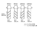
- FIG. 2 is a schematic diagram illustrating a typical example of the configuration of an end mill that can be used in the manufacturing method of the present invention.
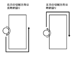
- FIG. 3 is a schematic plan view for explaining a difference in cutting direction between a case where the end mill has a right blade and a case where the end mill has a left blade. As shown in FIG.
- the configuration of the end mill is roughly classified into right blade right twist, right blade left twist, left blade right twist, and left blade left twist.
- the right blade refers to a structure that can be cut when rotated clockwise when viewed from the upper side (shank side); the left blade is counterclockwise when viewed from the upper side (shank side).
- right twist refers to a configuration in which the cutting edge extends obliquely to the upper right when viewed from the side;
- left twist refers to a configuration in which the cutting edge extends to the left obliquely upward when viewed from the side.
- the present inventors have developed a case where floating occurs in the surface protective film depending on the relationship between the discharge direction of the cutting dust of the end mill having a twisted blade and the arrangement of the surface protective film of the pressure-sensitive adhesive layer-attached optical laminate in the work. It has been found that there are cases where the surface protection film is not formed, and the problem of peeling failure of the surface protection film can be solved by causing the surface protection film to float.
- the pressure-sensitive adhesive layer-carrying optical laminate is scraped up (or scraped down) from the surface protective film side toward the separator side, and as a result, a strong cutting force is imparted in an oblique direction. It is possible to cause the surface protection film to float.
- the technical common sense of the industry that positively causes the surface protection film to have a float is completely absent. Due to the technical idea in the opposite direction, it is possible to obtain a machined pressure-sensitive adhesive layer-attached optical laminate in which peeling defects are suppressed. If the relationship between the configuration of the end mill and the stacked state of the work is reversed (that is, when the end mill has a right-handed right twist or a left-handed left twist, the work is formed as shown in FIG. When the work is formed as shown in FIG.
- the separator when the right blade has a left-handed twist or the left blade has a right-handed twist), the separator is floated while the surface protection film is not floated. As a result, it may not be possible to solve the problem of defective peeling of the surface protection film.
- the pressure-sensitive adhesive layer-carrying optical laminate may be cut into a rectangular shape, or may be cut into a shape similar to a rectangular shape, and may have an appropriate shape (for example, a circle) according to the purpose. It may be disconnected.
- the work W has outer peripheral surfaces (cutting surfaces) 1a and 1b facing each other and outer peripheral surfaces (cutting surfaces) 1c and 1d orthogonal to them.
- the work W is preferably clamped from above and below by a clamp means (not shown).
- the total thickness of the work is preferably 8 mm to 20 mm, more preferably 9 mm to 15 mm, and further preferably about 10 mm. With such a thickness, it is possible to prevent damage due to the pressing by the clamp means or the impact during cutting.
- the outer peripheral surface of the work W is cut by the end mill 60.
- Cutting is typically performed by bringing a cutting blade of an end mill into contact with the outer peripheral surface of the work W.
- the cutting may be performed over the entire circumference of the outer peripheral surface of the work, or may be performed only at a predetermined position.
- the end mill 60 includes a rotating shaft 61 extending in the stacking direction (vertical direction) of the works W, and a cutting blade 62 configured as the outermost diameter of the main body rotating about the rotating shaft 61.
- the cutting blade 62 is configured as the outermost diameter twisted along the rotary shaft 61, and shows a right blade right twist.
- the cutting blade 62 includes a cutting edge 62a, a rake face 62b, and a relief face 62c.
- the number of cutting blades 62 can be appropriately set depending on the purpose. Although the cutting blade in the illustrated example has three blades, the number of blades may be one continuous blade, two blades, four blades, or five or more blades. Good.
- blocking refers to a phenomenon in which optical layered bodies with an adhesive layer in a work adhere to each other with an adhesive agent on an end surface, and shavings of an adhesive agent attached to an end surface cause an optical layered layer with an adhesive layer. It will contribute to the adhesion between the bodies.
- the "outer diameter of the end mill” refers to a value obtained by doubling the distance from the rotary shaft 61 to the cutting edge 62a.
- the end mill may be a cantilever end mill having one end (upper end) held, or may be a double-ended end mill having both ends (upper end and lower end) held.
- the manufacturing method of the present invention includes non-linearly cutting the outer peripheral surface of the work.
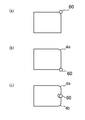
- the non-linear cutting includes, for example, as shown in FIG. 7, forming a concave portion 4c including a curved portion when the optical layered body with an adhesive layer is viewed in a plan view.
- the optical layered body with the pressure-sensitive adhesive layer having a shape in plan view as shown in FIG. 7 is produced, the outer periphery of the work is cut linearly, and chamfered portions 4a and 4b are provided at two corners of the outer periphery of the work.
- a concave portion (a concave portion including a curved portion) 4c is formed in the central portion of the outer peripheral surface on which the chamfered portions 4a and 4b are formed.
- the cutting conditions can be set appropriately according to the desired shape.
- the rotation speed of the end mill is preferably 1000 rpm to 60000 rpm, more preferably 10,000 rpm to 40,000 rpm.
- the feed speed of the end mill is preferably 500 mm/min to 10000 mm/min, more preferably 500 mm/min to 2500 mm/min.
- the number of cuts at the cutting location can be one cut, two cuts, three cuts or more.
- an optical layered product with a pressure-sensitive adhesive layer that has been machined can be obtained.
- the optical layered body with the pressure-sensitive adhesive layer that can be obtained by the production method of the present invention peeling defects of the surface protective film are suppressed.
- (1) Floating Occurrence Rate of Surface Protective Film An arbitrary number (preferably 100 or more) of the optical layered body with the pressure-sensitive adhesive layer after cutting was prepared, and the floating of the surface protective film was observed using a loupe or a microscope. The entire circumference of each optical layered body with an adhesive layer is observed. If a float of 1 ⁇ m or more is observed, the optical layered body with an adhesive layer is counted as a floating sample, and “(floating sample/observation quantity) The floating occurrence rate was calculated from “ ⁇ 100”.
- (2) Peeling success rate Fifty randomly cut optical laminates with pressure-sensitive adhesive layers obtained in Examples and Comparative Examples were randomly extracted, and the surface protective film was peeled for each (triggered peeling force 2 .9 N).
- the pressure-sensitive adhesive layer-attached polarizing plate obtained as described above was punched into a size of 5.7 inches (length 140 mm and width 65 mm), and a plurality of punched polarizing plates were stacked to form a work (total thickness of about 10 mm).
- a work total thickness of about 10 mm.
- clamps jigs
- chamfers are formed at two corners on the outer circumference of the work by end milling, and a recess (curve (Recesses including parts) were formed, and a polarizing plate with a pressure-sensitive adhesive layer was obtained by cutting as shown in FIG. 7.
- the feed rate of the end mill was 500 mm/min to 2000 mm/min, and the rotation speed was 5000 rpm to 30000 rpm.
- Example 2 Cutting was performed in the same manner as in Example 1 except that an end mill having a right blade with a right twist and a twist angle of 45° was used.
- the obtained polarizing plate with a pressure-sensitive adhesive layer that was processed was subjected to the same evaluations as in Example 1. The results are shown in Table 1.
Landscapes
- Physics & Mathematics (AREA)
- Engineering & Computer Science (AREA)
- Mechanical Engineering (AREA)
- General Physics & Mathematics (AREA)
- Optics & Photonics (AREA)
- Laminated Bodies (AREA)
- Polarising Elements (AREA)
- Milling Processes (AREA)
- Adhesives Or Adhesive Processes (AREA)
- Adhesive Tapes (AREA)
Abstract
表面保護フィルムの剥離不良が抑制された、切削加工された粘着剤層付光学積層体を簡便安価に製造し得る方法が提供される。本発明の切削加工された粘着剤層付光学積層体の製造方法は、粘着剤層付光学積層体を複数枚重ねてワークを形成すること、および、ねじれ刃を有するエンドミルを用いてワークの外周面を切削すること、を含む。粘着剤層付光学積層体は、光学フィルムと、光学フィルムの一方の側に配置された粘着剤層と、粘着剤層に剥離可能に仮着されたセパレーターと、光学フィルムのもう一方の側に剥離可能に仮着された表面保護フィルムと、を含む。本発明の製造方法においては、エンドミルの切削カスの排出方向にセパレーターが位置するようにして粘着剤層付光学積層体を重ねてワークを形成する。
Description
本発明は、切削加工された粘着剤層付光学積層体の製造方法に関する。
携帯電話、ノート型パーソナルコンピューター等の画像表示装置には、画像表示を実現し、および/または当該画像表示の性能を高めるために、種々の光学積層体(例えば、偏光板)が使用されている。代表的には、光学積層体には最外層として粘着剤層が設けられ、光学積層体の画像表示セルへの貼り合わせが可能とされている。実用的には、当該粘着剤層にはセパレーターが剥離可能に仮着され、実使用までの間粘着剤層を保護している。さらに、光学積層体の粘着剤層と反対側には、代表的には表面保護フィルムが剥離可能に仮着されている。近年、光学積層体の形状を所望の形状に加工することが望まれている。このような加工方法としては、例えば、エンドミルを用いた端面切削加工が挙げられる。
ここで、光学積層体を他の光学部材と貼り合わせる場合には、表面保護フィルムの剥離容易性(以下、単に剥離性と称する場合がある)が求められる。本発明はこのような課題を解決するためになされたものであり、その主たる目的は、表面保護フィルムの剥離不良が抑制された、切削加工された粘着剤層付光学積層体を簡便安価に製造し得る方法を提供することにある。
本発明の切削加工された粘着剤層付光学積層体の製造方法は、粘着剤層付光学積層体を複数枚重ねてワークを形成すること、および、ねじれ刃を有するエンドミルを用いて該ワークの外周面を切削すること、を含む。該粘着剤層付光学積層体は、光学フィルムと、該光学フィルムの一方の側に配置された粘着剤層と、該粘着剤層に剥離可能に仮着されたセパレーターと、該光学フィルムのもう一方の側に剥離可能に仮着された表面保護フィルムと、を含む。本発明の製造方法においては、該エンドミルの切削カスの排出方向に該セパレーターが位置するようにして該粘着剤層付光学積層体を重ねて該ワークを形成する。
1つの実施形態においては、上記エンドミルは右刃右ねじれまたは左刃左ねじれであり、上記セパレーターが上側に位置するようにして上記粘着剤層付光学積層体が重ねられて、ワークが形成されている。別の実施形態においては、上記エンドミルは右刃左ねじれまたは左刃右ねじれであり、上記セパレーターが下側に位置するようにして上記粘着剤層付光学積層体が重ねられて、ワークが形成されている。
1つの実施形態においては、上記セパレーターと上記粘着剤層との剥離力は、上記光学フィルムと上記表面保護フィルムとの剥離力よりも小さい。より具体的には、上記セパレーターと上記粘着剤層との剥離力は0.001N/10mm~1.0N/10mmであり、上記光学フィルムと上記表面保護フィルムとの剥離力は0.01N/10mm~5.0N/10mmである。
1つの実施形態においては、上記表面保護フィルムの厚みは、上記セパレーターの厚みよりも大きい。
1つの実施形態においては、上記表面保護フィルムは基材と粘着剤層とを有し、該粘着剤層の25℃における貯蔵弾性率G’は0.5×10⁶(Pa)~3.0×10⁶(Pa)である。
1つの実施形態においては、上記製造方法は、上記切削により上記表面保護フィルムの浮きを発生させる。1つの実施形態においては、上記表面保護フィルムの浮き量は1μm~1000μmである。
1つの実施形態においては、上記製造方法は、上記ワークの外周面を非直線的に切削することを含む。1つの実施形態においては、上記非直線的な切削は、上記粘着剤層付光学積層体を平面視した場合に曲線部を含む凹部を形成することを含む。1つの実施形態においては、上記曲線部の半径は5mm以下である。
1つの実施形態においては、上記光学フィルムは偏光子または偏光板である。
1つの実施形態においては、上記エンドミルは右刃右ねじれまたは左刃左ねじれであり、上記セパレーターが上側に位置するようにして上記粘着剤層付光学積層体が重ねられて、ワークが形成されている。別の実施形態においては、上記エンドミルは右刃左ねじれまたは左刃右ねじれであり、上記セパレーターが下側に位置するようにして上記粘着剤層付光学積層体が重ねられて、ワークが形成されている。
1つの実施形態においては、上記セパレーターと上記粘着剤層との剥離力は、上記光学フィルムと上記表面保護フィルムとの剥離力よりも小さい。より具体的には、上記セパレーターと上記粘着剤層との剥離力は0.001N/10mm~1.0N/10mmであり、上記光学フィルムと上記表面保護フィルムとの剥離力は0.01N/10mm~5.0N/10mmである。
1つの実施形態においては、上記表面保護フィルムの厚みは、上記セパレーターの厚みよりも大きい。
1つの実施形態においては、上記表面保護フィルムは基材と粘着剤層とを有し、該粘着剤層の25℃における貯蔵弾性率G’は0.5×10⁶(Pa)~3.0×10⁶(Pa)である。
1つの実施形態においては、上記製造方法は、上記切削により上記表面保護フィルムの浮きを発生させる。1つの実施形態においては、上記表面保護フィルムの浮き量は1μm~1000μmである。
1つの実施形態においては、上記製造方法は、上記ワークの外周面を非直線的に切削することを含む。1つの実施形態においては、上記非直線的な切削は、上記粘着剤層付光学積層体を平面視した場合に曲線部を含む凹部を形成することを含む。1つの実施形態においては、上記曲線部の半径は5mm以下である。
1つの実施形態においては、上記光学フィルムは偏光子または偏光板である。
本発明によれば、粘着剤層付光学積層体を複数枚重ねてワークを形成し、ねじれ刃を有するエンドミルを用いて該ワークの外周面を切削することを含む粘着剤層付光学積層体の製造方法において、エンドミルの切削カスの排出方向にセパレーターが位置するようにして粘着剤層付光学積層体を重ねてワークを形成することにより、表面保護フィルムの剥離不良が抑制された、切削加工された粘着剤層付光学積層体を簡便安価に製造し得る方法を実現することができる。
以下、図面を参照して本発明の具体的な実施形態について説明するが、本発明はこれらの実施形態には限定されない。なお、見やすくするために図面は模式的に表されており、さらに、図面における長さ、幅、厚み等の比率、ならびに角度等は、実際とは異なっている。
本発明の粘着剤層付光学積層体の製造方法は、粘着剤層付光学積層体を複数枚重ねてワークを形成すること;および、ねじれ刃を有するエンドミルを用いて該ワークの外周面を切削すること;を含む。粘着剤層付光学積層体は、光学フィルムと、光学フィルムの一方の側に配置された粘着剤層と、粘着剤層に剥離可能に仮着されたセパレーターと、光学フィルムのもう一方の側に剥離可能に仮着された表面保護フィルムと、を含む。本発明の実施形態においては、エンドミルの切削カスの排出方向にセパレーターが位置するようにして該粘着剤層付光学積層体を重ねて該ワークを形成する。便宜上、まず、本発明の粘着剤層付光学積層体の製造方法に用いられ得る粘着剤層付光学積層体の具体的な構成を説明し、次いで、本発明の粘着剤層付光学積層体の製造方法について説明する。
A.粘着剤層付光学積層体
図1は、本発明の製造方法に用いられ得る粘着剤層付光学積層体の一例を説明する概略断面図である。図示例の粘着剤層付光学積層体100は、光学フィルム10と、光学フィルム10の一方の側に配置された粘着剤層20と、粘着剤層20に剥離可能に仮着されたセパレーター30と、光学フィルム10のもう一方の側に剥離可能に仮着された表面保護フィルム40と、を含む。粘着剤層付光学積層体が画像表示装置に適用された場合、代表的には、セパレーター30が画像表示セル側に配置される。粘着剤層付光学積層体の実際の使用時にはセパレーター30は剥離除去され、粘着剤層20は、粘着剤層付光学積層体を画像表示装置(実質的には、画像表示セル)に貼り合わせるために用いられ得る。表面保護フィルム40は、代表的には、基材41と粘着剤層42とを有する。なお、粘着剤層20と区別するために、表面保護フィルムの粘着剤層42を「PF粘着剤層」と称する場合がある。表面保護フィルム40もまた、粘着剤層付光学積層体の実際の使用時には剥離除去される。本発明の実施形態においては、後述するような製造方法を採用することにより、表面保護フィルムの剥離不良が抑制された、切削加工された粘着剤層付光学積層体を実現することができる。すなわち、本発明の実施形態によれば、粘着剤層とセパレーターと表面保護フィルムとを含む粘着剤層付光学積層体に特有の課題である、表面保護フィルムの剥離不良を抑制することができる。
図1は、本発明の製造方法に用いられ得る粘着剤層付光学積層体の一例を説明する概略断面図である。図示例の粘着剤層付光学積層体100は、光学フィルム10と、光学フィルム10の一方の側に配置された粘着剤層20と、粘着剤層20に剥離可能に仮着されたセパレーター30と、光学フィルム10のもう一方の側に剥離可能に仮着された表面保護フィルム40と、を含む。粘着剤層付光学積層体が画像表示装置に適用された場合、代表的には、セパレーター30が画像表示セル側に配置される。粘着剤層付光学積層体の実際の使用時にはセパレーター30は剥離除去され、粘着剤層20は、粘着剤層付光学積層体を画像表示装置(実質的には、画像表示セル)に貼り合わせるために用いられ得る。表面保護フィルム40は、代表的には、基材41と粘着剤層42とを有する。なお、粘着剤層20と区別するために、表面保護フィルムの粘着剤層42を「PF粘着剤層」と称する場合がある。表面保護フィルム40もまた、粘着剤層付光学積層体の実際の使用時には剥離除去される。本発明の実施形態においては、後述するような製造方法を採用することにより、表面保護フィルムの剥離不良が抑制された、切削加工された粘着剤層付光学積層体を実現することができる。すなわち、本発明の実施形態によれば、粘着剤層とセパレーターと表面保護フィルムとを含む粘着剤層付光学積層体に特有の課題である、表面保護フィルムの剥離不良を抑制することができる。
光学フィルム10としては、切削加工(特に、非直線加工)が必要とされる用途に用いられ得る任意の適切な光学フィルムが挙げられる。光学フィルムは、単一層で構成されるフィルムであってもよく、積層体であってもよい。単一層で構成される光学フィルムの具体例としては、偏光子、位相差フィルムが挙げられる。積層体として構成される光学フィルムの具体例としては、偏光板(代表的には、偏光子と保護フィルムとの積層体)、タッチパネル用導電性フィルム、表面処理フィルム、ならびに、これらの単一層で構成される光学フィルムおよび/または積層体として構成される光学フィルムを目的に応じて適切に積層した積層体(例えば、反射防止用円偏光板、タッチパネル用導電層付偏光板)が挙げられる。
粘着剤層20としては、任意の適切な構成が採用され得る。粘着剤層を構成する粘着剤の具体例としては、アクリル系粘着剤、ゴム系粘着剤、シリコーン系粘着剤、ポリエステル系粘着剤、ウレタン系粘着剤、エポキシ系粘着剤、およびポリエーテル系粘着剤が挙げられる。粘着剤のベース樹脂を形成するモノマーの種類、数、組み合わせおよび配合比、ならびに、架橋剤の配合量、反応温度、反応時間等を調整することにより、目的に応じた所望の特性を有する粘着剤を調製することができる。粘着剤のベース樹脂は、単独で用いてもよく、2種以上を組み合わせて用いてもよい。透明性、加工性および耐久性などの観点から、アクリル系粘着剤が好ましい。粘着剤層を構成する粘着剤の詳細は、例えば、特開2014-115468号公報に記載されており、当該公報の記載は本明細書に参考として援用されている。粘着剤層20の厚みは、例えば10μm~100μmであり得る。粘着剤層20の25℃における貯蔵弾性率G’は、例えば1.0×10⁴(Pa)~1.0×10⁶(Pa)であり得る。なお、貯蔵弾性率は、例えば、動的粘弾性測定から求められ得る。
セパレーター30としては、任意の適切なセパレーターが採用され得る。具体例としては、剥離剤により表面コートされたプラスチックフィルム、不織布または紙が挙げられる。剥離材の具体例としては、シリコーン系剥離剤、フッ素系剥離剤、長鎖アルキルアクリレート系剥離剤が挙げられる。プラスチックフィルムの具体例としては、ポリエチレンテレフタレート(PET)フィルム、ポリエチレンフィルム、ポリプロピレンフィルムが挙げられる。セパレーターの厚みは、例えば10μm~100μmであり得る。
表面保護フィルム40は、上記のとおり、代表的には基材41と粘着剤層42とを有する。基材41の形成材料としては、例えば、ポリエチレンテレフタレート系樹脂等のエステル系樹脂、ノルボルネン系樹脂等のシクロオレフィン系樹脂、ポリプロピレン等のオレフィン系樹脂、ポリアミド系樹脂、ポリカーボネート系樹脂、これらの共重合体樹脂が挙げられる。好ましくは、エステル系樹脂(特に、ポリエチレンテレフタレート系樹脂)である。このような材料であれば、弾性率が十分に高く、搬送および/または貼り合わせ時に張力をかけても変形が生じにくいという利点がある。
基材41の弾性率は、例えば2.2kN/mm2~4.8kN/mm2であり得る。基材の弾性率がこのような範囲であれば、搬送および/または貼り合わせ時に張力をかけても変形が生じにくいという利点を有する。なお、弾性率は、JIS K 6781に準拠して測定される。
基材41の厚みは、例えば30μm~70μmであり得る。
粘着剤層(PF粘着剤層)42としては、任意の適切な構成が採用され得る。具体例としては、アクリル系粘着剤、ゴム系粘着剤、シリコーン系粘着剤、ポリエステル系粘着剤、ウレタン系粘着剤、エポキシ系粘着剤、およびポリエーテル系粘着剤が挙げられる。粘着剤のベース樹脂を形成するモノマーの種類、数、組み合わせおよび配合比、ならびに、架橋剤の配合量、反応温度、反応時間等を調整することにより、目的に応じた所望の特性を有する粘着剤を調製することができる。粘着剤のベース樹脂は、単独で用いてもよく、2種以上を組み合わせて用いてもよい。PF粘着剤層を構成する粘着剤は、ベース樹脂が活性水素含有官能基を有するポリマーを含むという特徴を有する。このようなベース樹脂であれば、所望の貯蔵弾性率を有するPF粘着剤層が得られ得る。PF粘着剤層を構成する粘着剤の詳細は、例えば、特開2018-123281号公報に記載されており、当該公報の記載は本明細書に参考として援用されている。PF粘着剤層42の厚みは、例えば10μm~100μmであり得る。PF粘着剤層42の25℃における貯蔵弾性率G’は、例えば0.5×10⁶(Pa)~3.0×10⁶(Pa)であり得る。貯蔵弾性率がこのような範囲であれば、粘着性と剥離性とのバランスに優れた粘着剤層(結果として、表面保護フィルム)を得ることができる。さらに、後述の製造方法によれば、表面保護フィルムに浮きを発生させることができ、その結果、浮き部分を掴みしろとして剥離点に応力を集中させることが容易となるので、許容可能な粘着性を維持しつつ、より優れた剥離性を実現することができる。
表面保護フィルム40の厚みは、例えば40μm~120μmであり得る。なお、表面保護フィルムの厚みとは、基材とPF粘着剤層の合計厚みをいう。
1つの実施形態においては、セパレーター30と粘着剤層20との剥離力(以下、セパレーターの剥離力とも称する)は、光学フィルム10と表面保護フィルム40(実質的には、PF粘着剤層42)との剥離力(以下、表面保護フィルムの剥離力とも称する)よりも小さい。多くの場合、セパレーターの剥離力よりも表面保護フィルムの剥離力が大きく、表面保護フィルムの剥離不良が発生しやすいところ、後述の製造方法によれば、表面保護フィルムの剥離不良が抑制された切削加工された粘着剤層付光学積層体を得ることができる。より具体的には、セパレーターの剥離力は好ましくは0.001N/10mm~1.0N/10mmであり、表面保護フィルムの剥離力は好ましくは0.01N/10mm~5.0N/10mmである。セパレーターの剥離力は、より好ましくは0.001~0.1N/10mmであり、さらに好ましくは0.005~0.03N/10mmである。表面保護フィルムの剥離力は、より好ましくは0.01~0.5N/10mmであり、さらに好ましくは0.035~0.1N/10mmである。セパレーターの剥離力と表面保護フィルムの剥離力との差(表面保護フィルムの剥離力-セパレーターの剥離力)は、好ましくは0.01N/10mm~1.0N/10mmである。後述の製造方法によれば、剥離力にこのような差があったとしても、表面保護フィルムの剥離不良が抑制された切削加工された粘着剤層付光学積層体を得ることができる。
1つの実施形態においては、表面保護フィルム40の厚みは、セパレーター30の厚みよりも大きい。後述の製造方法によれば、このように表面保護フィルムの厚みが分厚く大きな剥離力が必要とされる場合であっても、優れた剥離性を実現することができる。表面保護フィルムの厚みとセパレーターの厚みとの差(表面保護フィルムの厚み-セパレーターの厚み)は、好ましくは5μm~60μmである。後述の製造方法によれば、厚みにこのような差があったとしても、表面保護フィルムの剥離不良が抑制された切削加工された粘着剤層付光学積層体を得ることができる。
B.粘着剤層付光学積層体の製造方法
以下、粘着剤層付光学積層体の製造方法の代表例を説明する。最初に、本発明の特徴的な部分であるエンドミルの構成とワークの積層状態との関係を説明し、次いで、製造方法の概略を説明する。
以下、粘着剤層付光学積層体の製造方法の代表例を説明する。最初に、本発明の特徴的な部分であるエンドミルの構成とワークの積層状態との関係を説明し、次いで、製造方法の概略を説明する。
B-1.エンドミルの構成とワークの積層状態との関係
本発明の実施形態においては、上記のとおり、エンドミルの切削カスの排出方向にセパレーターが位置するようにして粘着剤層付光学積層体を重ねてワークを形成し、当該ワークの外周面を切削する。図2および図3を参照して具体的に説明する。図2は、本発明の製造方法に用いられ得るエンドミルの構成の代表例を説明する概略図である。図3は、エンドミルが右刃の場合と左刃の場合との切削方向の違いを説明する概略平面図である。図2に示すとおり、エンドミルの構成は、右刃右ねじれ、右刃左ねじれ、左刃右ねじれ、左刃左ねじれに大別される。図2に示すように、右刃とは、上側(シャンク側)から見て時計回りに回転したときに切削可能な構成をいい;左刃とは、上側(シャンク側)から見て反時計回りに回転したときに切削可能な構成をいう。図2にさらに示すように、右ねじれとは、刃先が側方からみて右斜め上方向に延びる構成をいい;左ねじれとは、刃先が側方からみて左斜め上方向に延びる構成をいう。右刃右ねじれおよび左刃左ねじれは、切削カスの排出方向が上方であり;右刃左ねじれおよび左刃右ねじれは、切削カスの排出方向が下方である。なお、図3に示すように、右刃の切削方向は代表的には反時計回りであり、左刃の切削方向は代表的には時計回りである。
本発明の実施形態においては、上記のとおり、エンドミルの切削カスの排出方向にセパレーターが位置するようにして粘着剤層付光学積層体を重ねてワークを形成し、当該ワークの外周面を切削する。図2および図3を参照して具体的に説明する。図2は、本発明の製造方法に用いられ得るエンドミルの構成の代表例を説明する概略図である。図3は、エンドミルが右刃の場合と左刃の場合との切削方向の違いを説明する概略平面図である。図2に示すとおり、エンドミルの構成は、右刃右ねじれ、右刃左ねじれ、左刃右ねじれ、左刃左ねじれに大別される。図2に示すように、右刃とは、上側(シャンク側)から見て時計回りに回転したときに切削可能な構成をいい;左刃とは、上側(シャンク側)から見て反時計回りに回転したときに切削可能な構成をいう。図2にさらに示すように、右ねじれとは、刃先が側方からみて右斜め上方向に延びる構成をいい;左ねじれとは、刃先が側方からみて左斜め上方向に延びる構成をいう。右刃右ねじれおよび左刃左ねじれは、切削カスの排出方向が上方であり;右刃左ねじれおよび左刃右ねじれは、切削カスの排出方向が下方である。なお、図3に示すように、右刃の切削方向は代表的には反時計回りであり、左刃の切削方向は代表的には時計回りである。
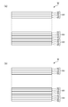
本発明の実施形態においては、上記のとおり、エンドミルの切削カスの排出方向にセパレーターが位置するようにして粘着剤層付光学積層体を重ねてワークを形成し、当該ワークの外周面を切削する。例えば、エンドミルが右刃右ねじれまたは左刃左ねじれである場合には、図4(a)に示すように、セパレーターが上側に位置するようにして粘着剤層付光学積層体を重ねてワークWを形成する。一方、エンドミルが右刃左ねじれまたは左刃右ねじれである場合には、図4(b)に示すように、セパレーターが下側に位置するようにして粘着剤層付光学積層体を重ねてワークWを形成する。本発明者らは、ねじれ刃を有するエンドミルの切削カスの排出方向とワークにおける粘着剤層付光学積層体の表面保護フィルムの配置との関係に応じて表面保護フィルムに浮きが発生する場合と発生しない場合があること、さらに、表面保護フィルムに浮きを発生させることにより表面保護フィルムの剥離不良という問題を解決できることを見出した。上記のような構成であれば、表面保護フィルム側からセパレーター側に向かって粘着剤層付光学積層体を削り上げる(または削り下げる)ことになり、その結果、強い切削力が斜め方向に付与される表面保護フィルムに浮きを発生させることができる。これにより、表面保護フィルムの剥離不良が抑制された切削加工された粘着剤層付光学積層体を得ることができる。表面保護フィルムの浮き量は、好ましくは1μm以上であり、より好ましくは20μm以上であり、さらに好ましくは50μm以上である。一方、浮き量は、好ましくは1000μm以下であり、より好ましくは500μm以下である。浮き量がこのような範囲であれば、他の不具合を発生させることなく、かつ、外観品位を許容可能な範囲に維持しつつ、表面保護フィルムの良好な剥離性を実現することができる。浮きは外観品位を低下させるので当業界においてはできるだけ発生を避けるものであるところ、本発明の実施形態によれば、表面保護フィルムに積極的に浮きを発生させるという当業界の技術常識とは全く逆方向の技術思想により、剥離不良が抑制された切削加工された粘着剤層付光学積層体を得ることができる。なお、エンドミルの構成とワークの積層状態との関係を逆にすると(すなわち、エンドミルが右刃右ねじれまたは左刃左ねじれである場合に図4(b)に示すようにワークを形成し、エンドミルが右刃左ねじれまたは左刃右ねじれである場合に図4(a)に示すようにワークを形成すると)、セパレーターに浮きが発生する一方で表面保護フィルムには浮きは発生しない。その結果、表面保護フィルムの剥離不良という問題を解消することはできない場合がある。
B-2.ワークの形成
次に、切削加工の概略を説明する。図5は、本発明の製造方法における切削加工を説明するための概略斜視図であり、本図にワークWが示されている。図5に示すように、粘着剤層付光学積層体を複数枚重ねたワークWが形成される。B-1項で説明したとおり、エンドミルの構成に応じて、図4(a)または図4(b)に示すようにワークWの積層状態が設定される。粘着剤層付光学積層体は、ワーク形成に際し、代表的には任意の適切な形状に切断されている。具体的には、粘着剤層付光学積層体は矩形形状に切断されていてもよく、矩形形状に類似する形状に切断されていてもよく、目的に応じた適切な形状(例えば、円形)に切断されていてもよい。ワークWは、互いに対向する外周面(切削面)1a、1bおよびそれらと直交する外周面(切削面)1c、1dを有している。ワークWは、好ましくは、クランプ手段(図示せず)により上下からクランプされている。ワークの総厚みは、好ましくは8mm~20mmであり、より好ましくは9mm~15mmであり、さらに好ましくは約10mmである。このような厚みであれば、クランプ手段による押圧または切削加工時の衝撃による損傷を防止し得る。粘着剤層付光学積層体は、ワークがこのような総厚みとなるように重ねられる。ワークを構成する粘着剤層付光学積層体の枚数は、例えば10枚~50枚であり得る。クランプ手段(例えば、治具)は、軟質材料で構成されてもよく硬質材料で構成されてもよい。軟質材料で構成される場合、その硬度(JIS A)は、好ましくは60°~80°である。硬度が高すぎると、クランプ手段による押し跡が残る場合がある。硬度が低すぎると、治具の変形により位置ずれが生じ、切削精度が不十分となる場合がある。
次に、切削加工の概略を説明する。図5は、本発明の製造方法における切削加工を説明するための概略斜視図であり、本図にワークWが示されている。図5に示すように、粘着剤層付光学積層体を複数枚重ねたワークWが形成される。B-1項で説明したとおり、エンドミルの構成に応じて、図4(a)または図4(b)に示すようにワークWの積層状態が設定される。粘着剤層付光学積層体は、ワーク形成に際し、代表的には任意の適切な形状に切断されている。具体的には、粘着剤層付光学積層体は矩形形状に切断されていてもよく、矩形形状に類似する形状に切断されていてもよく、目的に応じた適切な形状(例えば、円形)に切断されていてもよい。ワークWは、互いに対向する外周面(切削面)1a、1bおよびそれらと直交する外周面(切削面)1c、1dを有している。ワークWは、好ましくは、クランプ手段(図示せず)により上下からクランプされている。ワークの総厚みは、好ましくは8mm~20mmであり、より好ましくは9mm~15mmであり、さらに好ましくは約10mmである。このような厚みであれば、クランプ手段による押圧または切削加工時の衝撃による損傷を防止し得る。粘着剤層付光学積層体は、ワークがこのような総厚みとなるように重ねられる。ワークを構成する粘着剤層付光学積層体の枚数は、例えば10枚~50枚であり得る。クランプ手段(例えば、治具)は、軟質材料で構成されてもよく硬質材料で構成されてもよい。軟質材料で構成される場合、その硬度(JIS A)は、好ましくは60°~80°である。硬度が高すぎると、クランプ手段による押し跡が残る場合がある。硬度が低すぎると、治具の変形により位置ずれが生じ、切削精度が不十分となる場合がある。
B-3.切削加工
次に、ワークWの外周面をエンドミル60により切削する。切削は、代表的には、エンドミルの切削刃をワークWの外周面に当接させることにより行われる。切削は、ワークの外周面の全周にわたって行ってもよく、所定の位置のみに行ってもよい。
次に、ワークWの外周面をエンドミル60により切削する。切削は、代表的には、エンドミルの切削刃をワークWの外周面に当接させることにより行われる。切削は、ワークの外周面の全周にわたって行ってもよく、所定の位置のみに行ってもよい。
エンドミル60は、図6に示すように、ワークWの積層方向(鉛直方向)に延びる回転軸61と、回転軸61を中心として回転する本体の最外径として構成される切削刃62と、を有する。図示例では、切削刃62は、回転軸61に沿ってねじれた最外径として構成されており、右刃右ねじれを示している。切削刃62は、刃先62aと、すくい面62bと、逃がし面62cと、を含む。切削刃62の刃数は、目的に応じて適切に設定され得る。図示例における切削刃は3枚の構成であるが、刃数は連続した1枚であってもよく、2枚であってもよく、4枚であってもよく、5枚以上であってもよい。エンドミルの刃角度(図示例における切削刃のねじれ角θ)は、好ましくは20°~60°であり、より好ましくは30°~45°である。このような刃角度であれば、切削により表面保護フィルムに良好に浮きを発生させることができる。切削刃の逃がし面は、好ましくは、粗面化処理されている。粗面化処理としては、任意の適切な処理が採用され得る。代表例としては、ブラスト処理が挙げられる。逃がし面に粗面化処理を施すことにより、切削刃への粘着剤の付着が抑制され、結果として、ブロッキングが抑制され得る。エンドミルの外径は、好ましくは3mm~20mmである。なお、本明細書において「ブロッキング」とは、ワークにおける粘着剤層付光学積層体同士が端面の粘着剤で接着する現象をいい、端面に付着する粘着剤の削りカスが粘着剤層付光学積層体同士の接着に寄与することとなる。また、「エンドミルの外径」とは、回転軸61から刃先62aまでの距離を2倍したものをいう。エンドミルは、一端(上端)が保持された片持ちエンドミルであってもよいし、両端(上端と下端)が保持された両持ちエンドミルであってもよい。
1つの実施形態においては、本発明の製造方法は、ワークの外周面を非直線的に切削することを含む。非直線的な切削は、例えば図7に示すように、粘着剤層付光学積層体を平面視した場合に曲線部を含む凹部4cを形成することを含む。図7に示すような平面視形状の粘着剤層付光学積層体を作製する場合には、ワークの外周を直線的に切削するとともに、ワークの外周の2つの隅部に面取り部4a、4bを形成し、面取り部4a、4bが形成された外周面の中央部に凹部(曲線部を含む凹部)4cを形成する。このような凹部を形成することにより、凹部近傍に表面保護フィルムの浮きを発生させることができる。その結果、凹部から表面保護フィルムを剥離除去する場合の剥離性を向上させることができる。このような切削加工の一例について、図8(a)~図8(c)を参照して説明する。まず、図8(a)に示すように、図7の面取り部4aが形成される部分が面取り加工され、次いで、図8(b)に示すように、面取り部4bが形成される部分が面取り加工される。最後に、図8(c)に示すように、凹部(曲線部を含む凹部)4cが切削形成される。曲線部の半径は、好ましくは5mm以下であり、より好ましくは4mm以下であり、さらに好ましくは3mm以下である。なお、面取り部4aおよび4b、ならびに凹部4cの形成順序(切削順序)は限定されず、これらは任意の適切な順序で形成されればよい。
切削加工の条件は、所望の形状に応じて適切に設定され得る。エンドミルの回転数は、好ましくは1000rpm~60000rpmであり、より好ましくは10000rpm~40000rpmである。エンドミルの送り速度は、好ましくは500mm/分~10000mm/分であり、より好ましくは500mm/分~2500mm/分である。切削箇所の切削回数は、1回削り、2回削り、3回削りまたはそれ以上であり得る。
以上のようにして、切削加工された粘着剤層付光学積層体が得られ得る。本発明の製造方法により得られ得る粘着剤層付光学積層体は、表面保護フィルムの剥離不良が抑制されている。
以下、実施例により本発明を具体的に説明するが、本発明はこれらの実施例には限定されない。実施例における評価項目は以下のとおりである。
(1)表面保護フィルムの浮き発生率
切削加工後の粘着剤層付光学積層体を任意の数量(好ましくは100以上)準備し、ルーペもしくは顕微鏡を用いて表面保護フィルムの浮きを観察した。粘着剤層付光学積層体ごとに全周囲を観察し、1μm以上の浮きが観測されれば、その粘着剤層付光学積層体は浮き有サンプルとカウントし、「(浮き有サンプル/観察数量)×100」から浮き発生率を算出した。
(2)剥離成功率
実施例および比較例で得られた切削加工された粘着剤層付光学積層体を50枚無作為に抽出し、それぞれについて表面保護フィルムの剥離を行った(きっかけ剥離力2.9N)。50回の剥離のうち問題なく剥離できた回数を百分率で表し、剥離成功率とした。
(3)浮き量
実施例および比較例で得られた切削加工された粘着剤層付光学積層体における表面保護フィルムの浮き量をルーペもしくは顕微鏡で測定した。1つのワークにおける浮き量の最大値を浮き量とした。
切削加工後の粘着剤層付光学積層体を任意の数量(好ましくは100以上)準備し、ルーペもしくは顕微鏡を用いて表面保護フィルムの浮きを観察した。粘着剤層付光学積層体ごとに全周囲を観察し、1μm以上の浮きが観測されれば、その粘着剤層付光学積層体は浮き有サンプルとカウントし、「(浮き有サンプル/観察数量)×100」から浮き発生率を算出した。
(2)剥離成功率
実施例および比較例で得られた切削加工された粘着剤層付光学積層体を50枚無作為に抽出し、それぞれについて表面保護フィルムの剥離を行った(きっかけ剥離力2.9N)。50回の剥離のうち問題なく剥離できた回数を百分率で表し、剥離成功率とした。
(3)浮き量
実施例および比較例で得られた切削加工された粘着剤層付光学積層体における表面保護フィルムの浮き量をルーペもしくは顕微鏡で測定した。1つのワークにおける浮き量の最大値を浮き量とした。
<実施例1>
常法により、視認側から順に表面保護フィルム(60μm)/シクロオレフィン系保護フィルム(47μm)/偏光子(5μm)/シクロオレフィン系保護フィルム(24μm)/粘着剤層(20μm)/セパレーターの構成を有する粘着剤層付偏光板を作製した。なお、表面保護フィルムとしては、PET基材(50μm)/PF粘着剤層(10μm)の構成を有する表面保護フィルムを作製し、検証を行った。その際、粘着剤層(粘着剤)の貯蔵弾性率は0.5MPa~3.0MPaとなるように調整した。上記のようにして得られた粘着剤層付偏光板を5.7インチサイズ(縦140mmおよび横65mm程度)に打ち抜き、打ち抜いた偏光板を複数枚重ねてワーク(総厚み約10mm)とした。得られたワークをクランプ(治具)で挟んだ状態で、エンドミル加工により、ワークの外周の2つの隅部に面取り部を形成し、面取り部が形成された外周面の中央部に凹部(曲線部を含む凹部)を形成し、図7に示すような切削加工された粘着剤層付偏光板を得た。エンドミルの送り速度は500mm/分~2000mm/分であり、回転数は5000rpm~30000rpmであった。また、エンドミルは、右刃右ねじれ、ねじれ角30°のものを用いた。このエンドミルの切削カスの排出方向は上方であった。粘着剤層付偏光板は、セパレーターが上側に位置するようにして重ね合せてワークを形成した。切削による表面保護フィルムの浮き発生率は100%であった。得られた切削加工された粘着剤層付偏光板について、上記(2)および(3)の評価を行った。結果を表1に示す。
常法により、視認側から順に表面保護フィルム(60μm)/シクロオレフィン系保護フィルム(47μm)/偏光子(5μm)/シクロオレフィン系保護フィルム(24μm)/粘着剤層(20μm)/セパレーターの構成を有する粘着剤層付偏光板を作製した。なお、表面保護フィルムとしては、PET基材(50μm)/PF粘着剤層(10μm)の構成を有する表面保護フィルムを作製し、検証を行った。その際、粘着剤層(粘着剤)の貯蔵弾性率は0.5MPa~3.0MPaとなるように調整した。上記のようにして得られた粘着剤層付偏光板を5.7インチサイズ(縦140mmおよび横65mm程度)に打ち抜き、打ち抜いた偏光板を複数枚重ねてワーク(総厚み約10mm)とした。得られたワークをクランプ(治具)で挟んだ状態で、エンドミル加工により、ワークの外周の2つの隅部に面取り部を形成し、面取り部が形成された外周面の中央部に凹部(曲線部を含む凹部)を形成し、図7に示すような切削加工された粘着剤層付偏光板を得た。エンドミルの送り速度は500mm/分~2000mm/分であり、回転数は5000rpm~30000rpmであった。また、エンドミルは、右刃右ねじれ、ねじれ角30°のものを用いた。このエンドミルの切削カスの排出方向は上方であった。粘着剤層付偏光板は、セパレーターが上側に位置するようにして重ね合せてワークを形成した。切削による表面保護フィルムの浮き発生率は100%であった。得られた切削加工された粘着剤層付偏光板について、上記(2)および(3)の評価を行った。結果を表1に示す。
<比較例1>
粘着剤層付偏光板のセパレーターが下側に位置するようにして重ね合せてワークを形成したこと以外は実施例1と同様にして切削加工を行った。得られた切削加工された粘着剤層付偏光板を実施例1と同様の評価に供した。結果を表1に示す。
粘着剤層付偏光板のセパレーターが下側に位置するようにして重ね合せてワークを形成したこと以外は実施例1と同様にして切削加工を行った。得られた切削加工された粘着剤層付偏光板を実施例1と同様の評価に供した。結果を表1に示す。
<実施例2>
右刃右ねじれ、ねじれ角45°のエンドミルを用いたこと以外は実施例1と同様にして切削加工を行った。得られた切削加工された粘着剤層付偏光板を実施例1と同様の評価に供した。結果を表1に示す。
右刃右ねじれ、ねじれ角45°のエンドミルを用いたこと以外は実施例1と同様にして切削加工を行った。得られた切削加工された粘着剤層付偏光板を実施例1と同様の評価に供した。結果を表1に示す。
<比較例2>
粘着剤層付偏光板のセパレーターが下側に位置するようにして重ね合せてワークを形成したこと以外は実施例2と同様にして切削加工を行った。得られた切削加工された粘着剤層付偏光板を実施例1と同様の評価に供した。結果を表1に示す。
粘着剤層付偏光板のセパレーターが下側に位置するようにして重ね合せてワークを形成したこと以外は実施例2と同様にして切削加工を行った。得られた切削加工された粘着剤層付偏光板を実施例1と同様の評価に供した。結果を表1に示す。

<評価>
表1から明らかなように、本発明の実施例によれば、エンドミルの切削カスの排出方向にセパレーターが位置するようにして粘着剤層付光学積層体を重ねてワークを形成することにより、表面保護フィルムの剥離不良が抑制された、切削加工された粘着剤層付光学積層体を簡便安価に実現することができる。
表1から明らかなように、本発明の実施例によれば、エンドミルの切削カスの排出方向にセパレーターが位置するようにして粘着剤層付光学積層体を重ねてワークを形成することにより、表面保護フィルムの剥離不良が抑制された、切削加工された粘着剤層付光学積層体を簡便安価に実現することができる。
本発明の製造方法は、切削加工(特に、非直線加工)が必要とされる粘着剤層付光学積層体の製造に好適に用いられ得る。本発明の製造方法により得られる粘着剤層付光学積層体は、自動車のインストゥルメントパネルやスマートウォッチに代表される異形の画像表示部に好適に用いられ得る。
W ワーク
10 光学フィルム
20 粘着剤層
30 セパレーター
40 表面保護フィルム
60 エンドミル
100 粘着剤層付光学積層体
10 光学フィルム
20 粘着剤層
30 セパレーター
40 表面保護フィルム
60 エンドミル
100 粘着剤層付光学積層体
Claims (13)
- 粘着剤層付光学積層体を複数枚重ねてワークを形成すること、および、ねじれ刃を有するエンドミルを用いて該ワークの外周面を切削すること、を含み、
該粘着剤層付光学積層体が、光学フィルムと、該光学フィルムの一方の側に配置された粘着剤層と、該粘着剤層に剥離可能に仮着されたセパレーターと、該光学フィルムのもう一方の側に剥離可能に仮着された表面保護フィルムと、を含み、
該エンドミルの切削カスの排出方向に該セパレーターが位置するようにして該粘着剤層付光学積層体を重ねて該ワークを形成する、
切削加工された粘着剤層付光学積層体の製造方法。 - 前記エンドミルが右刃右ねじれまたは左刃左ねじれであり、
前記セパレーターが上側に位置するようにして前記粘着剤層付光学積層体が重ねられて、ワークが形成されている、
請求項1に記載の製造方法。 - 前記エンドミルが右刃左ねじれまたは左刃右ねじれであり、
前記セパレーターが下側に位置するようにして前記粘着剤層付光学積層体が重ねられて、ワークが形成されている、
請求項1に記載の製造方法。 - 前記セパレーターと前記粘着剤層との剥離力が、前記光学フィルムと前記表面保護フィルムとの剥離力よりも小さい、請求項1から3のいずれかに記載の製造方法。
- 前記セパレーターと前記粘着剤層との剥離力が0.001N/10mm~1.0N/10mmであり、前記光学フィルムと前記表面保護フィルムとの剥離力が0.01N/10mm~5.0N/10mmである、請求項4に記載の製造方法。
- 前記表面保護フィルムの厚みが、前記セパレーターの厚みよりも大きい、請求項1から5のいずれかに記載の製造方法。
- 前記表面保護フィルムが基材と粘着剤層とを有し、該粘着剤層の25℃における貯蔵弾性率G’が0.5×10⁶(Pa)~3.0×10⁶(Pa)である、請求項1から6のいずれかに記載の製造方法。
- 前記切削により前記表面保護フィルムの浮きを発生させる、請求項1から7のいずれかに記載の製造方法。
- 前記表面保護フィルムの浮き量が1μm~1000μmである、請求項8に記載の製造方法。
- 前記ワークの外周面を非直線的に切削することを含む、請求項1から9のいずれかに記載の製造方法。
- 前記非直線的な切削が、前記粘着剤層付光学積層体を平面視した場合に曲線部を含む凹部を形成することを含む、請求項10に記載の製造方法。
- 前記曲線部の半径が5mm以下である、請求項11に記載の製造方法。
- 前記光学フィルムが偏光子または偏光板である、請求項1から12のいずれかに記載の製造方法。
Priority Applications (2)
| Application Number | Priority Date | Filing Date | Title |
|---|---|---|---|
| CN202410949550.1A CN118837986A (zh) | 2019-02-20 | 2019-11-15 | 经切削加工的带粘合剂层的光学层叠体的制造方法 |
| CN201980092629.4A CN113454497B (zh) | 2019-02-20 | 2019-11-15 | 经切削加工的带粘合剂层的光学层叠体的制造方法 |
Applications Claiming Priority (2)
| Application Number | Priority Date | Filing Date | Title |
|---|---|---|---|
| JP2019028047A JP7257810B2 (ja) | 2019-02-20 | 2019-02-20 | 切削加工された粘着剤層付光学積層体の製造方法 |
| JP2019-028047 | 2019-02-20 |
Publications (1)
| Publication Number | Publication Date |
|---|---|
| WO2020170521A1 true WO2020170521A1 (ja) | 2020-08-27 |
Family
ID=72143563
Family Applications (1)
| Application Number | Title | Priority Date | Filing Date |
|---|---|---|---|
| PCT/JP2019/044859 Ceased WO2020170521A1 (ja) | 2019-02-20 | 2019-11-15 | 切削加工された粘着剤層付光学積層体の製造方法 |
Country Status (4)
| Country | Link |
|---|---|
| JP (2) | JP7257810B2 (ja) |
| CN (2) | CN113454497B (ja) |
| TW (2) | TWI835703B (ja) |
| WO (1) | WO2020170521A1 (ja) |
Families Citing this family (3)
| Publication number | Priority date | Publication date | Assignee | Title |
|---|---|---|---|---|
| JP7619772B2 (ja) * | 2020-04-09 | 2025-01-22 | 住友化学株式会社 | 光学積層体及び剥離方法 |
| JP2023134212A (ja) * | 2022-03-14 | 2023-09-27 | 日東電工株式会社 | 樹脂シートの製造方法 |
| EP4693826A1 (en) | 2023-03-31 | 2026-02-11 | Canon Kabushiki Kaisha | Power transmission device, power reception device, method implemented by power transmission device, and storage medium |
Citations (5)
| Publication number | Priority date | Publication date | Assignee | Title |
|---|---|---|---|---|
| JP2008275722A (ja) * | 2007-04-26 | 2008-11-13 | Sumitomo Chemical Co Ltd | 偏光板製品の梱包方法 |
| WO2013137389A1 (ja) * | 2012-03-14 | 2013-09-19 | 日東電工株式会社 | 光学フィルムロール |
| JP2017207585A (ja) * | 2016-05-17 | 2017-11-24 | 日東電工株式会社 | 光学積層体、ならびに該光学積層体を用いた光学フィルム片の製造方法 |
| WO2018016285A1 (ja) * | 2016-07-22 | 2018-01-25 | 日東電工株式会社 | 偏光板の製造方法およびその製造装置 |
| JP2018123221A (ja) * | 2017-01-31 | 2018-08-09 | 日東電工株式会社 | 表面保護フィルム、及び、光学部材 |
Family Cites Families (14)
| Publication number | Priority date | Publication date | Assignee | Title |
|---|---|---|---|---|
| JP3483505B2 (ja) * | 1999-08-11 | 2004-01-06 | 住友化学工業株式会社 | 積層フィルムの周縁の仕上げ方法 |
| JP2008203400A (ja) * | 2007-02-19 | 2008-09-04 | Nitto Denko Corp | 表面保護フィルム付偏光板、表面保護フィルム付液晶パネル、および画像表示装置 |
| JP5876990B2 (ja) * | 2011-03-25 | 2016-03-02 | 住友化学株式会社 | 端面加工偏光板の製造方法 |
| JP2013200376A (ja) * | 2012-03-23 | 2013-10-03 | Sumitomo Chemical Co Ltd | 端面加工偏光板の製造方法 |
| JP5267719B1 (ja) * | 2012-11-05 | 2013-08-21 | オムロン株式会社 | 樹脂製シートの製造方法、これを用いて製造した光学部材、この光学部材を用いた面光源装置、液晶表示装置、およびモバイル機器。 |
| JP6437230B2 (ja) * | 2013-09-04 | 2018-12-12 | 東友ファインケム株式会社Dongwoo Fine−Chem Co., Ltd. | 端面加工偏光板の製造方法 |
| JP6804843B2 (ja) * | 2015-01-30 | 2020-12-23 | 日東電工株式会社 | セパレータ付き光学用表面保護フィルム |
| JP6392799B2 (ja) * | 2016-02-16 | 2018-09-19 | 藤森工業株式会社 | 表面保護フィルム、及びそれが貼合された光学部品 |
| JP6696339B2 (ja) * | 2016-07-28 | 2020-05-20 | 三菱ケミカル株式会社 | Aei型シリコアルミノ燐酸塩及びその製造方法 |
| JP2018077355A (ja) * | 2016-11-09 | 2018-05-17 | 日東電工株式会社 | 積層光学フィルム、及び画像表示装置 |
| KR102510750B1 (ko) * | 2017-04-04 | 2023-03-15 | 스미또모 가가꾸 가부시키가이샤 | 프로텍트 필름 부착 편광판 및 액정 패널 |
| JP7232577B2 (ja) * | 2017-05-29 | 2023-03-03 | 日東電工株式会社 | 光学積層体の製造方法 |
| WO2019004043A1 (ja) * | 2017-06-27 | 2019-01-03 | 住友化学株式会社 | 粘着剤シート及び粘着剤層付フィルム |
| JP6612294B2 (ja) * | 2017-07-20 | 2019-11-27 | 住友化学株式会社 | 切削装置及び偏光板の製造方法 |
-
2019
- 2019-02-20 JP JP2019028047A patent/JP7257810B2/ja active Active
- 2019-11-15 CN CN201980092629.4A patent/CN113454497B/zh active Active
- 2019-11-15 WO PCT/JP2019/044859 patent/WO2020170521A1/ja not_active Ceased
- 2019-11-15 CN CN202410949550.1A patent/CN118837986A/zh active Pending
- 2019-11-27 TW TW112137319A patent/TWI835703B/zh active
- 2019-11-27 TW TW108143233A patent/TWI834766B/zh active
-
2023
- 2023-02-02 JP JP2023014534A patent/JP7378654B2/ja active Active
Patent Citations (5)
| Publication number | Priority date | Publication date | Assignee | Title |
|---|---|---|---|---|
| JP2008275722A (ja) * | 2007-04-26 | 2008-11-13 | Sumitomo Chemical Co Ltd | 偏光板製品の梱包方法 |
| WO2013137389A1 (ja) * | 2012-03-14 | 2013-09-19 | 日東電工株式会社 | 光学フィルムロール |
| JP2017207585A (ja) * | 2016-05-17 | 2017-11-24 | 日東電工株式会社 | 光学積層体、ならびに該光学積層体を用いた光学フィルム片の製造方法 |
| WO2018016285A1 (ja) * | 2016-07-22 | 2018-01-25 | 日東電工株式会社 | 偏光板の製造方法およびその製造装置 |
| JP2018123221A (ja) * | 2017-01-31 | 2018-08-09 | 日東電工株式会社 | 表面保護フィルム、及び、光学部材 |
Also Published As
| Publication number | Publication date |
|---|---|
| TWI835703B (zh) | 2024-03-11 |
| JP2023057095A (ja) | 2023-04-20 |
| CN113454497B (zh) | 2025-04-08 |
| JP2020134709A (ja) | 2020-08-31 |
| JP7257810B2 (ja) | 2023-04-14 |
| JP7378654B2 (ja) | 2023-11-13 |
| TWI834766B (zh) | 2024-03-11 |
| CN113454497A (zh) | 2021-09-28 |
| CN118837986A (zh) | 2024-10-25 |
| TW202043816A (zh) | 2020-12-01 |
| TW202403364A (zh) | 2024-01-16 |
Similar Documents
| Publication | Publication Date | Title |
|---|---|---|
| JP7378654B2 (ja) | 切削加工された粘着剤層付光学積層体の製造方法 | |
| JP7018349B2 (ja) | 切削加工された粘着剤層付光学積層体の製造方法 | |
| JP7378653B2 (ja) | 切削加工された粘着剤層付光学積層体の製造方法 | |
| CN111867765B (zh) | 非直线加工的树脂片的制造方法 | |
| JP7744116B2 (ja) | 光学フィルム切削用エンドミルおよび該エンドミルを用いた光学フィルムの製造方法 | |
| JP7018348B2 (ja) | 切削加工されたハードコート層付光学積層体の製造方法 | |
| JP7374297B2 (ja) | 貫通穴を有する粘着剤層付光学積層体の製造方法および該製造方法に用いられる貫通穴形成装置 | |
| JP7574278B2 (ja) | 貫通穴を有する粘着剤層付光学積層体の製造方法 | |
| JP7758570B2 (ja) | 光学フィルム切削用エンドミルおよび該エンドミルを用いた光学フィルムの製造方法 | |
| JP7573061B2 (ja) | 粘着剤層付光学積層体の製造方法 |
Legal Events
| Date | Code | Title | Description |
|---|---|---|---|
| 121 | Ep: the epo has been informed by wipo that ep was designated in this application |
Ref document number: 19916021 Country of ref document: EP Kind code of ref document: A1 |
|
| NENP | Non-entry into the national phase |
Ref country code: DE |
|
| 122 | Ep: pct application non-entry in european phase |
Ref document number: 19916021 Country of ref document: EP Kind code of ref document: A1 |
|
| WWG | Wipo information: grant in national office |
Ref document number: 201980092629.4 Country of ref document: CN |