WO2020168953A1 - 屏组件及电子设备 - Google Patents
屏组件及电子设备 Download PDFInfo
- Publication number
- WO2020168953A1 WO2020168953A1 PCT/CN2020/074830 CN2020074830W WO2020168953A1 WO 2020168953 A1 WO2020168953 A1 WO 2020168953A1 CN 2020074830 W CN2020074830 W CN 2020074830W WO 2020168953 A1 WO2020168953 A1 WO 2020168953A1
- Authority
- WO
- WIPO (PCT)
- Prior art keywords
- area
- identification
- screen assembly
- recognition
- fingerprint
- Prior art date
Links
Images


Classifications
-
- G—PHYSICS
- G06—COMPUTING; CALCULATING OR COUNTING
- G06V—IMAGE OR VIDEO RECOGNITION OR UNDERSTANDING
- G06V40/00—Recognition of biometric, human-related or animal-related patterns in image or video data
- G06V40/10—Human or animal bodies, e.g. vehicle occupants or pedestrians; Body parts, e.g. hands
- G06V40/12—Fingerprints or palmprints
- G06V40/13—Sensors therefor
- G06V40/1318—Sensors therefor using electro-optical elements or layers, e.g. electroluminescent sensing
-
- G—PHYSICS
- G06—COMPUTING; CALCULATING OR COUNTING
- G06V—IMAGE OR VIDEO RECOGNITION OR UNDERSTANDING
- G06V40/00—Recognition of biometric, human-related or animal-related patterns in image or video data
- G06V40/10—Human or animal bodies, e.g. vehicle occupants or pedestrians; Body parts, e.g. hands
- G06V40/12—Fingerprints or palmprints
- G06V40/1365—Matching; Classification
Definitions
- the embodiments of the present application relate to the technical field of electronic products, in particular to a screen assembly and an electronic device.
- the embodiments of the present application provide a screen assembly and an electronic device to realize large-area fingerprint recognition and low cost.
- an embodiment of the present application provides a screen assembly.
- the screen assembly can be applied to electronic equipment.
- the screen assembly includes a display panel and an identification panel on the non-light emitting side of the display panel.
- the identification panel and the display panel are stacked.
- the display panel is used for displaying images.
- the two sides of the display panel are respectively a light-emitting side and a non-light-emitting side, wherein the light-emitting side is the side where the display panel emits display light.
- the display panel includes a plurality of identification areas.
- a non-recognition area is formed between the two adjacent and spaced recognition areas.
- the recognition panel includes a plurality of image sensors.
- the photosensitive surfaces of the plurality of image sensors are used to collect user fingerprint images located in the plurality of identification areas in a one-to-one correspondence.
- the photosensitive surface of the image sensor can convert the light image formed thereon into an electrical signal that is proportional to the light image.
- the ratio of the total area of all the identification areas to the total area of all the non-identification areas is greater than or equal to 1:5.
- the identification panel including the multiple image sensors is located on the non-light emitting side of the display panel, so the multiple image sensors can collect fingerprint images under the screen, and the multiple image sensors need not Occupying the peripheral space of the display panel, the area of the display panel is increased, which is conducive to the narrow frame of the screen assembly, so that the screen occupancy of the screen assembly is relatively large, and the electronic device using the screen assembly The screen occupancy is relatively large.
- the photosensitive surfaces of the plurality of image sensors collect partial user fingerprint images located on the light-emitting side of the multiple identification areas in a one-to-one correspondence, and do not collect some fingerprint images located on the light-emitting side of the non-recognition area Therefore, the photosensitive surfaces of the multiple image sensors perform partial collection of user fingerprint images on the light-emitting side of the display panel, instead of collecting all of them, so that the total area of the photosensitive surfaces of the multiple image sensors can be reduced. The cost of the identification panel and the screen assembly can be reduced.
- the photosensitive surfaces of the multiple image sensors collect The total area of the partial fingerprint image (that is, the effective collection area) can meet the minimum collection area required by the fingerprint recognition process, so that the screen assembly can meet the basic recognition requirements, while reducing the photosensitive surface of the multiple image sensors The total area is reduced, thereby reducing the cost of the multiple image sensors, and also reducing the cost of the screen assembly. Since the screen assembly can meet the identification requirements and has a low cost, the screen assembly can realize large-area fingerprint recognition (full-screen fingerprint recognition or large-screen fingerprint recognition) without significantly increasing the cost. That is, the screen assembly and the electronic device using the screen assembly can realize large-area fingerprint recognition and have low cost.
- the ratio of the total area of all the identification areas to the total area of all the non-identification areas is in the range of 1:2 to 2:1.
- the range of "A" to "B” includes endpoint A and endpoint B.
- the upper limit of the ratio of the total area of all the identification areas to the total area of all the non-identification areas in the fingerprint coverage area is not strictly limited in this application.
- the larger the ratio the higher the recognition accuracy.
- the lower the ratio the lower the cost.
- the screen component can realize full-screen fingerprint recognition.
- the fingerprint coverage area may be located at any position of the display area of the display panel. That is, the entire display area of the display panel can respond to the user's operation to form a corresponding fingerprint coverage area.
- the screen assembly can realize large-screen fingerprint recognition.
- the fingerprint coverage area may be located in a designated range of the display area of the display panel. For example, a part of the display area of the display panel is a designated position, and this part of the area can form a corresponding fingerprint coverage area in response to a user's operation.
- the area of the designated range is relatively large.
- the specified range can be half or more of the upper or lower screen of the screen assembly, and can be half or more of the left or right screen of the screen assembly.
- the fingerprint coverage area responds to user operations. That is, the location of the fingerprint coverage area is customized by the user.
- the screen assembly may sense a user's touch area, and the touch area forms the fingerprint coverage area. At this time, the shape of the fingerprint coverage area changes with the shape of the user's touch area.
- the screen component may activate the preset fingerprint coverage area corresponding to the touch location by sensing the user's touch location, and the fingerprint coverage area covers the touch location.
- the shape of the fingerprint coverage area may be a circle, an oval, a square, a racetrack, or the like.
- the shape of the fingerprint coverage area may also be similar or the same as the shape of the user's finger.
- the shape of the fingerprint coverage area can also be customized by the user. The embodiment of the present application does not strictly limit the specific shape of the fingerprint coverage area.
- the area covered by the fingerprint is in the range of 35 square millimeters to 200 square millimeters.
- the area covered by the fingerprint may range from 64 square millimeters to 144 square millimeters.
- the fingerprint coverage area includes at least two identification areas. At this time, the area of each recognition area is small.
- the images collected by the photosensitive surfaces of the image sensors corresponding to at least two of the identification regions are stitched into a final comparison image. Since the comparison image is formed by stitching multiple images, the comparison image is more accurate, which is beneficial to improve the fingerprint recognition accuracy of the electronic device using the screen assembly.
- the smaller the area of each recognition area the more the comparison images are stitched together, the higher the image quality of the comparison images, and the accuracy of fingerprint recognition Higher, and the larger number of image sensors also brings high cost; and the larger the area of each recognition area, although the number of image sensors can be reduced to reduce costs, the number of stitched images included in the comparison image is reduced , The image quality of the comparison image decreases, and the accuracy of fingerprint recognition decreases. Therefore, when designing the area of a single recognition area in the embodiment of the present application, it is necessary to consider both the recognition accuracy requirement and the cost requirement.
- the photosensitive surface of each image sensor includes a plurality of sensor units arranged in an array.
- the sensing unit may be a complementary metal oxide semiconductor (complementary metal oxide semiconductor, CMOS) sensor, or a thin film transistor (thin film transistor, TFT) sensor.
- CMOS complementary metal oxide semiconductor
- TFT thin film transistor
- the substrate of the image sensor adopts a semiconductor material.
- the substrate of the image sensor adopts insulating materials such as glass or organic medium.
- the shape and area of each of the identification regions may be the same or different. This application is described by taking as an example that the shapes and areas of the identification regions are the same.
- the arrangement of the multiple recognition areas may be regular or random. .
- the arrangement of the multiple identification areas can be described as an example.
- the multiple identification areas are arranged at intervals in the first direction. That is, in the first direction, the non-recognition area is arranged between any two adjacent recognition areas. At this time, in the first direction, the distance between any two adjacent identification areas has a first size, and the length of each identification area has a second size.
- the first size may be greater than, equal to, or smaller than the second size, and the embodiment of the present application does not strictly limit the size relationship between the two.
- the two fingerprint coverage areas are arranged at intervals in the first direction, when the two fingerprint coverage areas are located at different positions of the display panel, the two fingerprint coverage areas
- the number of photosensitive surfaces of the corresponding image sensors is the same or similar, thereby ensuring that the screen assembly can obtain a sufficient effective collection area in different usage scenarios, so that the fingerprint recognition accuracy of the electronic device is high.
- the plurality of identification regions are arranged at intervals in a second direction, and the second direction is perpendicular to the first direction. That is, in the second direction, non-recognition areas are arranged between any two adjacent recognition areas. At this time, in the second direction, the distance between any two adjacent identification areas has a third dimension, and the length of each identification area has a fourth dimension.
- the third size may be greater than, equal to, or smaller than the fourth size, and the embodiment of the present application does not strictly limit the size relationship between the two.
- the two fingerprint coverage areas corresponding to the two fingerprints are located at different positions of the display panel.
- the number of photosensitive surfaces of the image sensor is the same or more similar, which further ensures that the screen assembly can obtain a sufficient effective collection area in different usage scenarios, so that the fingerprint recognition accuracy of the electronic device is higher.
- the arrangement of the plurality of identification regions in the first direction is the same as the arrangement in the second direction. At this time, the reliability of the screen assembly to obtain a sufficient effective collection area under different usage scenarios is higher, and the fingerprint recognition accuracy of the electronic device is higher.
- the arrangement of the plurality of identification regions in the first direction may be different from the arrangement in the second direction.
- the plurality of identification areas are arranged in rows at intervals in the first direction, and arranged in rows at intervals in the second direction, and the second direction is perpendicular to the first direction.
- Each of the identification areas in the two adjacent rows of the identification areas are arranged in different columns. At this time, each of the identification areas in two adjacent columns of the identification areas are arranged in different columns.
- the number of identification areas included in any two fingerprint coverage areas with different positions of the screen assembly is very similar, that is, the photosensitive surface of the image sensor corresponding to the two fingerprint coverage areas
- the numbers are very similar, and the screen assembly can obtain sufficient effective collection area in different usage scenarios, so that the fingerprint recognition accuracy of the electronic device is higher.
- the ratio of the total area of all the recognition areas to the total area of all the non-recognition areas is in the range of 1:0.8 to 1:1.2.
- the distance between two adjacent identification areas may be equal to, slightly greater than, or slightly less than the length of the identification area.
- the distance between two adjacent identification areas may also be equal to, slightly greater than or slightly less than the length of the identification areas.
- the screen assembly can comprehensively consider the requirements of manufacturing tolerances, assembly tolerances, total image collection area, cost, etc., to obtain higher product yield, fingerprint recognition accuracy, and lower cost.
- the multiple identification areas include multiple identification area groups.
- Each of the identification area groups includes at least two of the identification areas adjacent to each other. Any two adjacent identification area groups are arranged at intervals with each other. Wherein, that at least two identification areas are adjacent to each other means that the distance between two adjacent identification areas of the same identification area group is much smaller than the distance between two adjacent identification area groups.
- the non-recognition area is formed between any two adjacent recognition area groups.
- the plurality of identification area groups are arranged at intervals in a first direction, and arranged at intervals or continuously in a second direction, and the second direction is perpendicular to the first direction.
- each of the recognition area groups includes at least two recognition areas adjacent to each other, and any two adjacent recognition area groups are arranged at intervals with each other, the arrangement of the recognition areas The method is more diversified, which is conducive to meeting the fingerprint identification requirements of different electronic devices.
- Each of the recognition area groups includes at least two recognition areas, which also enables the recognition area to collect continuous images in a small area, so that the final comparison image formed by the screen assembly is spliced by at least two continuous images As a result, the final comparison image is easier to compare with the standard image in the electronic device, and the fingerprint recognition accuracy of the electronic device is higher.
- the fingerprint coverage area includes at least two identification area groups.
- the final comparison image formed by the screen assembly is formed by stitching together the images collected by at least two of the identification area groups, and the image quality is high, so that the fingerprint recognition of the electronic device using the screen assembly The accuracy is high.
- a single image sensor includes one photosensitive surface. At this time, the overall volume of the image sensor changes with the area of its photosensitive surface, and the area of the photosensitive surface is designed to be small, so that the overall volume of the image sensor is small, which is beneficial to reducing the cost of the image sensor.
- a single image sensor includes a plurality of photosensitive surfaces.
- multiple photosensitive surfaces can be integrated into the same image sensor to reduce the difficulty of the cutting process of the image sensor, thereby taking into account the small size and easy processing requirements of the image sensor.
- the multiple photosensitive surfaces of the same image sensor may be arranged at intervals with each other, or may be arranged adjacent to each other.
- the identification panel further includes a substrate and an optical layer.
- the substrate is located on the non-light emitting side of the display panel.
- the plurality of image sensors are fixed on the side of the substrate facing the display panel.
- the photosensitive surface of each image sensor is arranged away from the substrate, that is, arranged facing the display panel.
- the optical layer is located between the plurality of image sensors and the display panel.
- the optical layer is used to image the user fingerprint image located on the light emitting side of the identification area onto the corresponding photosensitive surface of the image sensor.
- the screen assembly processes the light reflected by the user's fingerprint through the optical layer to form a corresponding collection image on the corresponding photosensitive surface of the image sensor, and the collection image corresponds to the user's fingerprint image.
- the optical layer can change the light state, so the structure and size of the optical layer can be set to make the photosensitive surface of the image sensor and the The relative positional relationship of the display panel changes, which makes the structure of the screen assembly more diversified, and the application range of the screen assembly is wider.
- the photosensitive surfaces of the plurality of image sensors may directly face the plurality of identification regions in a one-to-one correspondence.
- the optical layer changes the propagation direction of the light slightly, which can reduce the risk of distortion of the light during the propagation process and the resulting inaccuracy of the final comparison image, so that the electronics of the screen assembly The fingerprint recognition accuracy of the device is high.
- the optical layer can change the propagation direction of light, so the relative positional relationship between the light-sensitive surfaces of the plurality of image sensors may be slightly different from the relative positional relationship of the plurality of identification regions.
- a single image sensor includes multiple photosensitive surfaces, and the multiple photosensitive surfaces are adjacent to each other.
- the plurality of identification regions corresponding to the plurality of photosensitive surfaces are arranged at intervals.
- the propagation direction of the light is changed by the optical layer, so that the light entering from these identification areas is converged and injected into a plurality of adjacent photosensitive surfaces, thereby realizing image collection.
- the substrate may be a rigid printed circuit board (printed circuit board, PCB).
- the substrate may include a flexible printed circuit (FPC) and a reinforcement board, and the reinforcement board and the flexible printed circuit board are laminated.
- PCB printed circuit board
- FPC flexible printed circuit
- the multiple image sensors may be directly bonded to the substrate in a die attach manner.
- the plurality of image sensors may be connected into an integrated package structure using a fan-out process, and then the package structure is integrally bonded to the substrate.
- the identification panel further includes a package.
- the package is located on a side of the substrate facing the display panel, and is arranged around the plurality of image sensors. At this time, the package encapsulates the plurality of image sensors into an integrated package structure.
- the package may adopt a fan-out process to package a plurality of the image sensors.
- the optical layer covers the package and the plurality of image sensors. At this time, the optical layer may be an integral structure.
- the package can first encapsulate the plurality of image sensors into an integrated packaging structure, and then attach the packaging structure to the substrate, and then attach the optical layer that is also an integrated structure. Covering the package and the plurality of image sensors, the assembly process steps of the screen assembly are few and the process difficulty is low, which is beneficial to reduce the production cost of the screen assembly.
- the optical layer includes a plurality of optical parts.
- the plurality of optical parts are located on the plurality of image sensors in one-to-one correspondence.
- the optical part is located on the side of the corresponding image sensor where the image is collected, that is, located above the photosensitive surface of the image sensor.
- the identification panel further includes a plurality of packages.
- the plurality of packages and the plurality of optical parts are arranged in one-to-one correspondence. Each package body is used to package the corresponding optical part and the image sensor into an integral unit assembly.
- the identification panel also includes a package.
- the package is located on a side of the substrate facing the display panel, and is arranged around the plurality of image sensors and the plurality of optical parts.
- the image sensor and the optical part located above it may first form a unit assembly, and after a plurality of the unit assemblies are fixed to the substrate, a plurality of the units are connected through the package.
- the components and the substrate are packaged into an integrated structure.
- the image sensor and the optical part located above it may first form a unit assembly, and after a plurality of the unit assemblies are packaged into an integrated structure by the packaging member, the structure is bonded To the substrate to complete the assembly.
- the corresponding optical part and the image sensor can form a unit assembly, and then a plurality of the unit assemblies are fixed to the substrate according to specific arrangement requirements, so the screen assembly can Without changing the type of material, different identification panels can be formed by changing the positions of the unit components, which is beneficial to the batching and multi-modeling of the screen components.
- the optical layer includes a plurality of collimators.
- the collimator is used to transform divergent light into collimated light.
- the plurality of collimators are arranged directly opposite to the photosensitive surfaces of the plurality of image sensors in a one-to-one correspondence.
- the plurality of collimators form a collection image with a ratio of 1:1 on the photosensitive surface of the image sensor. Since the plurality of collimators can collimate the light reflected by the fingerprint of the user, the image quality of the captured image is higher, and the screen assembly can form a higher quality comparison image, so that the The fingerprint recognition accuracy of electronic equipment is relatively high.
- the collimator is used to image the acquired image with a ratio of 1:1, the area of the light-sensitive surface of the image sensor is similar to the area of the recognition area on the display panel. Considering the tolerances of the multiple image sensors during assembly, a reasonable escape can be reserved between the two image sensors that are close to each other to improve the assembly accuracy and product yield of the screen assembly.
- each of the collimators can be directly formed on the wafer level processing technology.
- the photosensitive surface of the image sensor For example, a multi-layer mask process may be used to deposit or etch a collimating hole structure on the photosensitive surface of the image sensor to form the collimator.
- each of the collimators may be a thin film with collimating holes formed first, and then each of the collimators is attached to the corresponding photosensitive surface of the image sensor.
- the optical layer may be an integrated structure including a plurality of collimators.
- the optical layer includes a plurality of light-transmitting small holes.
- the optical layer may include a substrate and a light-shielding film, and the light-shielding film is located on a side of the substrate facing the display panel.
- the substrate is made of light-transmitting material, such as glass or polycarbonate (PC).
- the light-shielding film has the plurality of light-transmitting small holes.
- the light-shielding film adopts a light-shielding material.
- the plurality of light-transmitting small holes are arranged directly opposite to the photosensitive surfaces of the plurality of image sensors in a one-to-one correspondence.
- a first distance is formed between the center of each light-transmitting hole and the light-emitting surface of the display panel, and a second distance is formed between the center of each light-transmitting hole and the photosensitive surface of the image sensor, the first distance being greater than the second distance spacing.
- the plurality of light-transmitting small holes form a collection image with an object image ratio X:1 on the photosensitive surface of the image sensor.
- X is greater than 1.
- the area of the collected image is smaller than the area of the recognition area on the display panel. Therefore, when the area of the recognition area remains unchanged, the area of the photosensitive surface of the image sensor can be reduced, so that The cost of the image sensor is reduced, and the cost of the screen assembly is reduced.
- the area of the recognition area corresponding to the image sensor increases, and the splicing of multiple recognition areas may adopt redundant splicing, thereby improving the Describes the accuracy of fingerprint recognition of electronic equipment.
- the screen assembly can reduce the area of the photosensitive surface of the image sensor by adjusting the size of the first interval and the second interval, or increase the area of the recognition area corresponding to the photosensitive surface of the image sensor .
- the light-emitting surface of the display panel is a surface of the display panel away from the identification panel.
- the non-light-emitting surface of the display panel is arranged opposite to the light-emitting surface of the display panel.
- a gap is formed between the non-light-emitting surface of the display panel and the center of the light-transmitting hole. The size of the first spacing can be adjusted by adjusting the size of the spacing.
- the base of the optical layer has a thickness (a dimension in a direction perpendicular to the photosensitive surface of the image sensor).
- the size of the second gap can be adjusted by adjusting the thickness of the substrate.
- the screen assembly further includes a transparent adhesive layer, and the adhesive layer is bonded between the display panel and the optical layer.
- the adhesive layer is filled between the display panel and the optical layer.
- the adhesive layer can adhere the optical layer and the display panel, and can also prevent light from affecting the quality of the captured image due to scattering of the air layer.
- the adhesive layer can be a transparent optical glue. In an embodiment, the adhesive layer can also cover the package at the same time.
- the optical layer includes a plurality of lenses.
- the plurality of lenses are arranged facing the photosensitive surfaces of the plurality of image sensors in a one-to-one correspondence.
- the lens is used for imaging and reducing the user fingerprint image to the photosensitive surface of the image sensor.
- the lens is used to collect light.
- the lens is used to image and reduce the user fingerprint image to the photosensitive surface of the image sensor, and the area ratio of the captured image formed on the photosensitive surface of the image sensor to the corresponding recognition area Less than 1, that is, the ratio of the object image is greater than 1.
- the area of the collected image is smaller than the area of the recognition area on the display panel. Therefore, when the area of the recognition area remains unchanged, the area of the photosensitive surface of the image sensor can be reduced, so that The cost of the image sensor is reduced, and the cost of the screen assembly is reduced.
- the area of the photosensitive surface of the image sensor remains unchanged, the area of the recognition area corresponding to the photosensitive surface of the image sensor increases, and the splicing of multiple recognition areas may adopt redundant splicing, Therefore, the accuracy of fingerprint recognition of the electronic device is improved.
- a single lens may include one or more sub-lenses.
- the sub-lens is a convex lens.
- the multiple sub-lens may be multiple convex lenses, or a combination of concave and convex lenses.
- the lens may also be a plane lens made with a metamaterial structure.
- an embodiment of the present application also provides an electronic device.
- the electronic device includes a housing and the screen assembly described in any one of the above.
- the screen assembly is installed on the housing.
- the screen assembly since the screen assembly has a larger display area, the screen occupancy of the electronic device is relatively large. Since the screen assembly can reduce the total area of the photosensitive surfaces of the plurality of image sensors under the condition of having a sufficient effective collection area, thereby reducing the cost of the plurality of image sensors, the cost of the screen assembly is lower , The electronic device can realize large-area fingerprint recognition without significantly affecting the fingerprint recognition performance with low cost.
- FIG. 1 is a schematic structural diagram of an electronic device provided by an embodiment of the present application.
- FIG. 2 is a schematic diagram of the structure of the screen assembly of the electronic device shown in FIG. 1;
- Fig. 3 is a schematic structural diagram of the structure of the screen assembly shown in Fig. 2 at line A-A in an embodiment
- FIG. 4 is a schematic structural diagram of the structure of the screen assembly shown in FIG. 2 at line A-A in another embodiment
- FIG. 5A is a schematic diagram of a partial structure of a display panel of the screen assembly shown in FIG. 2 in an embodiment
- FIG. 5B is a schematic diagram of the recognition area and the non-recognition area of the display panel shown in FIG. 5A in one arrangement;
- FIG. 5C is a schematic diagram of the recognition area and the non-recognition area of the display panel shown in FIG. 5A in another arrangement;
- 5D is a schematic diagram of the recognition area and the non-recognition area of the display panel shown in FIG. 5A in yet another arrangement;
- 6A is a schematic diagram of a part of the structure of the display panel of the screen assembly shown in FIG. 2 in another embodiment
- 6B is a schematic diagram of a part of the structure of the display panel of the screen assembly shown in FIG. 2 in another embodiment
- 6C is a schematic diagram of a part of the structure of the display panel of the screen assembly shown in FIG. 2 in still another embodiment
- FIG. 7 is a schematic structural diagram of the screen assembly shown in FIG. 3 in the first embodiment
- Fig. 8A is a schematic structural diagram of the screen assembly shown in Fig. 7 in the first embodiment
- FIG. 8B is a schematic structural diagram of the screen assembly shown in FIG. 7 in the second embodiment
- FIG. 8C is a schematic structural diagram of the screen assembly shown in FIG. 7 in the third embodiment.
- Fig. 9 is a schematic structural diagram of the screen assembly shown in Fig. 3 in the second embodiment.
- FIG. 10A is a schematic structural diagram of the screen assembly shown in FIG. 9 in the first embodiment
- FIG. 10B is a schematic structural diagram of the screen assembly shown in FIG. 9 in the second embodiment
- Fig. 10C is a schematic structural diagram of the screen assembly shown in Fig. 9 in the third embodiment.
- FIG. 1 is a schematic structural diagram of an electronic device 100 according to an embodiment of the present application.
- the electronic device 100 may be a mobile phone, a tablet computer, an e-reader, a notebook computer, a vehicle-mounted device, or a wearable device.
- the electronic device 100 is a mobile phone as an example for description.
- the electronic device 100 includes a housing 10 and a screen assembly 20.
- the screen assembly 20 is installed on the housing 10.
- the housing 10 includes a frame and a back cover.
- the frame is arranged around the periphery of the back cover.
- the screen assembly 20 is installed on the side of the frame away from the back cover. That is, the screen assembly 20 and the back cover are respectively installed on both sides of the frame.
- the screen assembly 20 is usually placed toward the user, and the back cover is placed away from the user.
- the frame and the back cover can be assembled to form an integrated structure.
- the frame and the back cover can also be an integral structure.
- the screen assembly 20 integrates a display function, a touch sensing function, and a fingerprint image collection function.
- the screen assembly 20 can collect a user's fingerprint image and form a corresponding comparison image.
- the electronic device 100 further includes a circuit board 30 and a control module 40 located on the circuit board 30.
- the circuit board 30 and the control module 40 are housed inside the housing 10.
- the control module 40 may include at least one communication interface, a bus, at least one processor, and at least one memory. At least one communication interface, at least one processor, and at least one memory can communicate with each other through a bus. At least one communication interface is used to receive and send data.
- the screen assembly 20 is connected to one of the communication interfaces. The screen assembly 20 can transmit the data of the comparison image corresponding to the user's fingerprint image to the processor.
- At least one memory is used to store program codes.
- the program code includes fingerprint identification code.
- At least one processor can be used to execute the above application code. For example, at least one processor can execute fingerprint recognition codes to realize fingerprint recognition. In this application, "at least one" includes one or two cases.
- FIG. 2 is a schematic diagram of the structure of the screen assembly 20 of the electronic device 100 shown in FIG. 1
- FIG. 3 is the structure of the screen assembly 20 shown in FIG. 2 at line AA.
- Schematic diagram of the structure In an embodiment Schematic diagram of the structure.
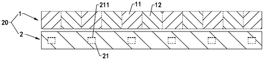
- the screen assembly 20 includes a display panel 1 and an identification panel 2 located on the non-light emitting side of the display panel 1.
- the identification panel 2 and the display panel 1 are stacked.
- the display panel 1 is used to display images.
- the two sides of the display panel 1 are respectively a light-emitting side and a non-light-emitting side, wherein the light-emitting side is the side where the display panel 1 emits display light.
- the recognition panel 2 includes a plurality of image sensors 21.
- the display panel 1 includes a plurality of identification areas 11.
- a non-recognition area 12 is formed between two adjacent and spaced recognition areas 11.
- the photosensitive surfaces 211 of the multiple image sensors 21 are used to collect user fingerprint images located on the light emitting side of the display panel 1 in a one-to-one correspondence.
- the photosensitive surfaces 211 of the multiple image sensors 21 are used to collect user fingerprint images located in the multiple identification areas 11 in a one-to-one correspondence.
- the image sensor 21 can convert the captured image (light image) formed on its photosensitive surface 211 into an electrical signal that is proportional to the captured image.
- the ratio of the total area of all recognition areas 11 to the total area of all non-recognition areas 12 is greater than or equal to 1:5.
- the recognition panel 2 including multiple image sensors 21 is located on the non-light emitting side of the display panel 1. Therefore, the multiple image sensors 21 can collect fingerprint images under the screen, and the multiple image sensors 21 do not need to occupy the display panel 1 In the surrounding space, the area of the display panel 1 can be increased, which facilitates the narrowing of the frame of the screen assembly 20, so that the screen assembly 20 has a larger screen occupancy, and the electronic device 100 using the screen assembly 20 has a larger screen occupancy.
- the photosensitive surfaces 211 of the multiple image sensors 21 collect partial user fingerprint images located on the light-emitting side of the multiple identification areas 11 in a one-to-one correspondence, and do not collect partial fingerprint images located on the light-emitting side of the non-recognition area 12, Therefore, the photosensitive surface 211 of the plurality of image sensors 21 collects part of the user's fingerprint image on the light-emitting side of the display panel 1, instead of collecting all of them, so that the total area of the photosensitive surface 211 of the plurality of image sensors 21 can be reduced, and the identification panel 2 and The cost of the screen assembly 20 can be reduced.
- the ratio of the total area of all the recognition areas 11 to the total area of all the non-recognition areas 12 in the fingerprint coverage area 3 is greater than or equal to 1:5, the local fingerprints collected by the photosensitive surfaces 211 of the multiple image sensors 21
- the total area of the image (that is, the effective collection area) can meet the minimum collection area required by the fingerprint recognition process, so that the screen assembly 20 can reduce the total area of the photosensitive surface 211 of the multiple image sensors 211 while meeting the basic recognition requirements.
- the cost of the multiple image sensors 21 is reduced, and the production cost of the screen assembly 20 is also reduced.
- the screen assembly 20 can meet the identification requirements and has a low cost, the screen assembly 20 can realize large-area fingerprint identification (full-screen fingerprint identification or large-screen fingerprint identification) without significantly increasing the cost. That is, the screen assembly 20 and the electronic device 100 using the screen assembly 20 can realize large-area fingerprint recognition with low cost.
- the fingerprint coverage area 3 includes the area within the area contour. If half of the area of a certain recognition area 11 or other preset ratios (such as full, two-thirds, one-third, three-quarters, one-quarter, one-fifth, etc.) are within the area contour, the recognition area 11 is a fingerprint Cover the area within area 3.
- the non-recognized area 12 is the area within the fingerprint coverage area 3; when the non-recognized area 12 is an integrated area (see Figure 5C below): the non-recognized area 12 is located within the area contour Is the area within the fingerprint coverage area 3.
- the ratio of the total area of all the recognition areas 11 to the total area of all the non-recognition areas 12 is in the range of 1:2 to 2:1.
- the range of "A" to "B” includes endpoint A and endpoint B.
- the upper limit of the ratio of the total area of all identification areas 11 to the total area of all non-identification areas 12 in the fingerprint coverage area 3 is not strictly limited in this application.
- the larger the ratio the higher the recognition accuracy.
- the lower the ratio the lower the cost.
- the ratio needs to take into account the recognition accuracy and cost.
- the screen assembly 20 can perform well. Take into account the needs of recognition accuracy and cost.
- the screen assembly 20 can realize full-screen fingerprint recognition.
- the fingerprint coverage area 3 can be located anywhere in the display area of the display panel 1. That is, the entire display area of the display panel 1 can respond to the user's operation to form a corresponding fingerprint coverage area 3.
- the screen assembly 20 can realize large-screen fingerprint recognition.
- the fingerprint coverage area 3 may be located in a designated range of the display area of the display panel 1. For example, a part of the display area of the display panel 1 is a designated position, and this part of the area can form a corresponding fingerprint coverage area 3 in response to a user's operation.
- the area of the designated range is relatively large.
- the specified range can be half or more of the upper or lower screen of the screen assembly, and can be half or more of the left or right screen of the screen assembly.
- the fingerprint coverage area responds to user operations. That is, the location of the fingerprint coverage area is customized by the user.
- the screen assembly may sense a user's touch area, and the touch area forms the fingerprint coverage area. At this time, the shape of the fingerprint coverage area changes with the shape of the user's touch area.
- the screen component may activate the preset fingerprint coverage area corresponding to the touch location by sensing the user's touch location, and the fingerprint coverage area covers the touch location.
- the shape of the fingerprint coverage area 3 may be a circle, an oval, a square, a racetrack, or the like.
- the shape of the fingerprint coverage area 3 may also be similar or the same as the shape of the user's finger.
- the shape of the fingerprint coverage area 3 can also be customized by the user.
- the embodiment of the present application does not strictly limit the specific shape of the fingerprint coverage area 3.
- the shape of the fingerprint coverage area 3 in FIG. 2 is a circle as an example for illustration.
- the embodiment of the present application also discloses a fingerprint identification method of the electronic device 100, and the method can be applied to the electronic device 100 in the embodiment of the present application.
- the method includes:
- Step 1 The screen component 20 captures the user's touch position and forms touch information.
- the first touch information includes position information of the user's finger.
- the first touch information includes position information (that is, coordinates) of the first point 311.
- the second touch information includes location information (that is, coordinates) of the second point 321.
- the touch layer in the screen assembly 20 can be used to step the user's touch action and form touch information.
- Step 2 The control module 40 activates the light source corresponding to the fingerprint coverage area 3 according to the touch information.
- the corresponding fingerprint coverage area 3 is an area covered by a preset shape with the position of the user's finger as the center or base point.
- the corresponding fingerprint coverage area 3 is the first fingerprint coverage area 31.
- the corresponding fingerprint coverage area 3 is the second fingerprint coverage area 32.
- the light source of the corresponding fingerprint coverage area 3 can be the recognition area 11 and the non-recognition area 12 located in the fingerprint coverage area 3, or it can be a luminous covering the fingerprint coverage area 3. area.
- Step 3 The control module 40 activates the photosensitive surface 211 of the image sensor 21 corresponding to the fingerprint coverage area 3 according to the touch information.
- each image sensor 21 includes a photosensitive surface 211.
- the photosensitive surface 211 of the image sensor 21 corresponding to the first fingerprint coverage area 31 is the photosensitive surface 211 of the four image sensors 21 used to collect the first fingerprint coverage area 31 in FIG. 2.
- the photosensitive surface of the image sensor 21 corresponding to the second fingerprint coverage area 32 is the photosensitive surface 211 of the five image sensors 21 used to collect the second fingerprint coverage area 32 in FIG. 2.
- the required photosensitive surfaces 211 may also be activated, and the unnecessary photosensitive surfaces 211 may not work, so as to reduce energy consumption.
- Step 4 The control module 40 reads the comparison image data of the photosensitive surface 211 of the image sensor 21 corresponding to the fingerprint coverage area 3.
- the compared image data corresponds to the fingerprint image of the user.
- the control module 40 can simultaneously read the data of the photosensitive surfaces 211 of the multiple image sensors 21 corresponding to the fingerprint coverage area 3, and can also smoothly read the photosensitive surfaces of the multiple image sensors 21 corresponding to the fingerprint coverage area 3. 211 data.
- Step 5 The control module 40 extracts and compares the feature information in the image data to match the template. If the matching is successful, the fingerprint recognition is passed, and the electronic device 100 performs subsequent corresponding operations (for example, unlocking operations such as screen unlocking, APP unlocking, payment unlocking, etc.). If the matching fails, the fingerprint recognition fails, and the electronic device 100 does not perform subsequent corresponding operations.
- subsequent corresponding operations for example, unlocking operations such as screen unlocking, APP unlocking, payment unlocking, etc.
- the control module 40 activates the corresponding light source and the photosensitive surface 211 of the image sensor 21 according to the user's touch position
- the electronic device 100 only needs to activate the required part of the light source and part of the image sensor 21 during the fingerprint recognition process.
- the photosensitive surface 211 of the image sensor can be used for image collection, and only the comparison image data formed by the photosensitive surface 211 of the image sensor 21 can be processed to realize the matching judgment. Therefore, the overall power consumption of the electronic device 100 is low, and the image is taken. Short time and fast recognition speed.
- the area of the fingerprint coverage area 3 is in the range of 35 square millimeters to 200 square millimeters.
- the area of the fingerprint coverage area 3 may be in the range of 64 square millimeters to 144 square millimeters.
- the fingerprint coverage area 3 usually includes at least two identification areas 11. At this time, the area of each recognition area 11 is small.
- the images collected by the photosensitive surface 211 of the image sensor 21 corresponding to the at least two identification regions 11 are stitched into a final comparison image. Since the comparison image is formed by stitching multiple images, the comparison image is more accurate, which is beneficial to improve the fingerprint recognition accuracy of the electronic device 100 to which the screen assembly 20 is applied.
- the fingerprint coverage area 3 has a basic collection area
- the smaller the area of each recognition area 11 the more the comparison images are stitched together, the higher the image quality of the comparison images, the fingerprint recognition
- the accuracy of the image sensor 21 is higher, and the larger number of image sensors 21 also brings about the problem of high cost; and the larger the area of each recognition area 11, although the number of image sensors 21 can be reduced to reduce the cost, the comparison of the image
- the number of spliced images included decreases, the image quality of the comparison images decreases, and the accuracy of fingerprint recognition decreases. Therefore, when designing the area of a single recognition area 11 in the embodiment of the present application, both the recognition accuracy requirement and the cost requirement need to be considered.
- the photosensitive surface 211 of each image sensor 21 includes a plurality of sensor units arranged in an array.
- the sensing unit may adopt a complementary metal oxide semiconductor (complementary metal oxide semiconductor, CMOS) sensor, or a thin film transistor (TFT) sensor.
- CMOS complementary metal oxide semiconductor
- TFT thin film transistor
- the substrate of the image sensor 21 adopts a semiconductor material.
- the substrate of the image sensor 21 is made of insulating materials such as glass or organic medium.
- the sensing unit in each image sensor 21 is used to sense visible light. Then, part or all of the display panel 1 allows visible light to pass through, and the display panel 1 is a transparent display screen. At this time, the visible light reflected by the user's fingerprint can enter the image sensor 21 after passing through the display panel 1, so that the screen assembly 20 can smoothly collect the user's fingerprint image.
- the display light emitted by the display panel 1 can be used as the sensing light of the electronic device 100 in fingerprint recognition.
- the sensing light can be collected by the image sensor 21 after being reflected by the user's fingerprint to form a comparison image corresponding to the fingerprint image.
- the sensing unit in each image sensor 21 is used to sense invisible light. Invisible light such as near infrared, infrared, near ultraviolet, ultraviolet, etc. Then, part or all of the display panel 1 allows invisible light to pass through. At this time, the display panel 1 may allow visible light to pass through or block visible light, which is not strictly limited in this application.
- the electronic device 100 further includes a light source for emitting invisible light.
- the light source can be independent of the screen assembly 20 or integrated in the screen assembly 20.
- the invisible light emitted by the light source can be collected by the image sensor 21 after being reflected by the fingerprint of the user, so that the screen assembly 20 forms a comparison image corresponding to the fingerprint image.
- the display panel 1 may be an organic light-emitting diode (OLED) panel, a liquid crystal display (LCD), a quantum dot light emitting diode (QLED) panel, or a micro-sized light emitting diode.
- OLED organic light-emitting diode
- LCD liquid crystal display
- QLED quantum dot light emitting diode
- uLED micro-sized light emitting diode.
- Diode micro light-emitting diode, uLED
- a single image sensor 21 includes a photosensitive surface 211.
- the overall volume of the image sensor 21 changes with the area of the photosensitive surface 211, and the area of the photosensitive surface 211 is designed to be small, so that the overall volume of the image sensor 21 is small, which is beneficial to reduce the cost of the image sensor 21.
- FIG. 4 is a schematic structural diagram of the structure of the screen assembly 20 shown in FIG. 2 at the line A-A in another embodiment.
- a single image sensor 21 includes multiple photosensitive surfaces 211.
- multiple photosensitive surfaces 211 can be integrated into the same image sensor 21 to reduce the difficulty of the cutting process of the image sensor 21, thereby taking into account the small size and easy processing requirements of the image sensor 21.
- the multiple photosensitive surfaces 211 of the same image sensor 21 may be arranged at intervals or adjacent to each other.
- the plurality of photosensitive surfaces 211 may be coplanar.
- each recognition area 11 may be the same or different. This application will be described by taking as an example that the shapes and areas of the recognition regions 11 are the same.
- the arrangement of the plurality of recognition areas 11 may be regular or random.
- the arrangement of the multiple identification areas 11 can be described as an example.
- FIG. 5A is a partial structural diagram of the display panel 1 of the screen assembly 20 shown in FIG. 2 in an embodiment.
- the recognition area 11 is shown as a square filled with oblique lines
- the non-recognition area 12 is shown as a square without filling.
- the plurality of identification regions 11 are arranged in rows at intervals in the first direction X, and arranged in rows at intervals in the second direction Y, and the second direction Y is perpendicular to the first direction X.
- Each of the identification regions 11 in the two adjacent rows of identification regions 11 are arranged in different columns.
- the recognition areas 11 in the two adjacent columns of recognition areas 11 are all arranged in different columns.
- first direction X may be parallel to the width direction of the screen assembly 20 (also called lateral direction), and the second direction Y is parallel to the length direction of the screen assembly 20 (also called vertical direction). In other embodiments, the first direction X and the second direction Y can be reversed.
- the identification areas 11 of odd rows are arranged in odd columns, and the identification areas 11 of even rows are arranged in even columns.
- Row 1, row 3, row 5, row 7, and row 9 are odd rows.
- Rows 2, 4, 6, 8, and 10 are even-numbered rows.
- the first, third, fifth, seventh, and ninth columns are odd columns.
- the second, fourth, sixth, eighth, and tenth columns are even-numbered columns.
- the odd-numbered row identification areas 11 can also be arranged in even-numbered columns, and the even-numbered row identification areas 11 are arranged in odd-numbered columns.
- the number of identification areas 11 included in any two fingerprint coverage areas 3 with different positions of the screen assembly 20 is very close, that is, the photosensitive surface 211 of the image sensor 21 corresponding to the two fingerprint coverage areas 3
- the numbers are very similar, and the screen assembly 20 can obtain a sufficient effective collection area in different usage scenarios, so that the fingerprint recognition accuracy of the electronic device 100 is higher.
- the ratio of the total area of all identification areas 11 to the total area of all non-identification areas is in the range of 1:0.8 to 1:1.2.
- the distance between two adjacent identification areas 11 may be equal to, slightly greater than, or slightly less than the length of the identification area 11.
- the distance between two adjacent identification areas 11 may also be equal to, slightly greater than, or slightly less than the length of the identification area 11.
- the screen assembly 20 can comprehensively consider the requirements of manufacturing tolerances, assembly tolerances, total image collection area, cost, etc., to obtain higher product yield, fingerprint recognition accuracy, and lower cost.
- FIG. 5B is a schematic diagram of the recognition area 11 and the non-recognition area 12 of the display panel 1 shown in FIG. 5A in an arrangement.
- the recognition area 11 is indicated by a grid filled with oblique lines
- the non-recognition area 12 is indicated by an unfilled space.
- the display panel 1 includes a plurality of non-recognition areas 12, and the multiple non-recognition areas 12 are separated by the recognition area 11.
- the length L1 of each identification area 11 is equal to the distance L2 between two adjacent identification areas 11.
- the distance L2 is equal to the length of the non-identification area 12 in the first direction X.
- the length L3 of each identification area 11 is equal to the distance L4 between two adjacent identification areas 11.
- the interval L4 is equal to the length of the non-identification area 12 in the second direction Y.
- the shape and size of the non-recognition area 12 are the same as the recognition area 11.
- the circular fingerprint coverage area 3 is taken as an example in FIG. 5A for illustration.
- the size of each recognition area 11 is 3 mm*3 mm.
- the fingerprint coverage area 3 is a circular area with a diameter of 9 mm.
- the third fingerprint coverage area 33 four identification areas 11 are included.
- the photosensitive surfaces 211 of the four image sensors 21 in the identification panel 2 corresponding to the four identification areas 11 are used to collect user fingerprint images.
- the effective collection area is 36 square millimeters, which can meet the minimum collection area requirements for fingerprint identification.
- the fourth fingerprint coverage area 34 five identification areas 11 are included.
- the photosensitive surfaces 211 of the five image sensors 21 in the identification panel 2 corresponding to the five identification areas 11 are used to collect user fingerprint images.
- the effective collection area is 45 square millimeters, which can meet the minimum collection area requirements for fingerprint identification.
- the number of photosensitive surfaces 211 of the image sensor 21 corresponding to any two fingerprint coverage areas 3 with different positions of the screen assembly 20 is very similar, and the screen assembly 20 can obtain sufficient effective collection area in different usage scenarios. .
- FIG. 5C is a schematic diagram of the recognition area 11 and the non-recognition area 12 of the display panel 1 shown in FIG. 5A in another arrangement.
- the recognition area 11 is indicated by a grid filled with oblique lines
- the non-recognition area 12 is indicated by an unfilled space.
- the non-identification area 12 is an integral area.
- the length L1 of each identification area 11 is smaller than the distance L2 between two adjacent identification areas 11.
- the distance L2 is the length in the first direction X of the part of the non-recognition area 12 located between two adjacent recognition areas 11.
- the length L3 of each identification area 11 is smaller than the distance L4 between two adjacent identification areas 11.
- the distance L4 is the length in the second direction Y of a part of the non-recognition area 12 located between two adjacent recognition areas 11.
- FIG. 5D is a schematic diagram of the recognition area 11 and the non-recognition area 12 of the display panel 1 shown in FIG. 5A in another arrangement.
- the recognition area 11 is indicated by a grid filled with oblique lines
- the non-recognition area 12 is indicated by an unfilled space.
- the display panel 1 includes a plurality of non-recognition areas 12, and the multiple non-recognition areas 12 are separated by the recognition area 11.
- the length L1 of each identification area 11 is greater than the distance L2 between two adjacent identification areas 11.
- the distance L2 is the length of the non-identification area 12 in the first direction X.
- the length L3 of each identification area 11 is greater than the distance L4 between two adjacent identification areas 11.
- the distance L4 is the length of the non-identification area 12 in the second direction Y.
- the shape of the non-recognition area 12 is the same or similar to the recognition area 11, and the area of the non-recognition area 12 is smaller than the area of the recognition area 11. In this embodiment, there is a small amount of redundancy in the image formed after the images on the multiple recognition regions 11 are spliced, and can be processed into a suitable comparison image to improve the accuracy of fingerprint recognition of the electronic device 100.
- FIG. 6A is a partial structural diagram of the display panel 1 of the screen assembly 20 shown in FIG. 2 in another embodiment.
- the identification area 11 in FIG. 6A is shown as a square filled with oblique lines, and the non-recognition area 12 is shown as a square without filling.
- a plurality of identification areas 11 are arranged at intervals in the first direction X. That is, in the first direction X, non-recognition areas 12 are arranged between any two adjacent recognition areas 11. At this time, in the first direction X, the distance between any two adjacent identification areas 11 has a first size, and the length of each identification area 11 has a second size.
- the first size is also the length in the first direction X of the part of the non-recognition area 12 located between the two recognition areas 11.
- the first size may be greater than, equal to, or smaller than the second size, and the embodiment of the present application does not strictly limit the size relationship between the two.
- a plurality of identification regions 11 are continuously arranged in a row in the second direction Y, and the second direction Y is perpendicular to the first direction X.
- the two identification regions 11 adjacent to each other in the second direction Y are adjacent to each other. That is, the distance between two identification areas 11 adjacent to each other in the second direction Y (which can be zero, negative or positive) is much smaller than the two identification areas 11 adjacent to each other in the first direction X the distance between.
- the display panel 1 includes a plurality of non-recognition areas 12. Any two adjacent rows of identification regions 11 form a strip-shaped non-identification region 12 between them.
- the plurality of identification areas 11 may also be arranged in other ways in the second direction Y, for example, arranged at intervals.
- a circular fingerprint coverage area 3 is taken as an example for illustration.
- the size of each recognition area 11 is 2 mm*2 mm.
- the fingerprint coverage area 3 is a circular area with a diameter of 10 mm.
- the fifth fingerprint coverage area 35 includes 10 identification areas 11.
- the photosensitive surfaces 211 of the ten image sensors 21 in the identification panel 2 corresponding to the ten identification regions 11 are used to collect user fingerprint images.
- the effective collection area is 40 square millimeters, which can meet the minimum collection area requirements for fingerprint identification.
- the sixth fingerprint coverage area 36 includes 15 identification areas 11.
- the photosensitive surfaces 211 of the 15 image sensors 21 in the recognition panel 2 corresponding to the 15 recognition areas 11 are used to collect user fingerprint images.
- the effective collection area is 60 square millimeters, which can meet the minimum collection area requirements for fingerprint identification.
- the image sensors corresponding to the two fingerprint coverage areas 3 is the same or similar, thereby ensuring that the screen assembly 20 can obtain a sufficient effective collection area in different usage scenarios, so that the fingerprint recognition accuracy of the electronic device 100 is high.
- FIG. 6B is a partial structural diagram of the display panel 1 of the screen assembly 20 shown in FIG. 2 in still another embodiment.
- the identification area 111 in FIG. 6C is shown as a square filled with oblique lines, and the non-recognition area 112 is shown as a square without filling.
- the multiple identification areas 111 are arranged at intervals in the first direction. That is, in the first direction, at least one non-recognition area 112 is arranged between any two adjacent recognition areas 111.
- the first direction is the row direction or the column direction of the area array formed by the plurality of areas 11.
- the plurality of identification areas 111 and the plurality of non-identification areas 112 may be alternately arranged one by one, alternately arranged one by two, or alternately arranged two by one, which is not strictly limited in this application.
- the plurality of identification regions 111 are arranged at intervals in a second direction, and the second direction is perpendicular to the first direction. That is, in the second direction, at least one non-recognition area 112 is arranged between any two adjacent recognition areas 111.
- the first size is larger than the second size, for example, the first size is equal to twice the second size.
- the third size is greater than the fourth size, for example, the third size is equal to twice the fourth size.
- the plurality of identification regions 11 are continuously arranged in the diagonal direction of the first direction X and the second direction Y.
- the display panel 1 includes a plurality of non-recognition areas 12. A non-recognition area 12 is formed between two adjacent recognition areas 11 in the diagonal direction.
- the non-recognition area 12 is roughly in the shape of a stepped bar.
- each area 11 is 2 mm*2 mm.
- the fingerprint coverage area 3 is a circular area with a diameter of 10 mm.
- eight identification areas 11 are included.
- the photosensitive surfaces 211 of the eight image sensors 21 in the identification panel 2 corresponding to the eight identification areas 11 are used to collect user fingerprint images.
- the effective collection area is 32 square millimeters, which can meet the minimum collection area requirements for fingerprint identification.
- the eighth fingerprint coverage area 38 nine identification areas 11 are included.
- the photosensitive surfaces 211 of the nine image sensors 21 in the identification panel 2 corresponding to the nine identification areas 11 are used to collect user fingerprint images. At this time, the effective collection area is 36 square millimeters, which can meet the minimum collection area requirements for fingerprint identification.
- the image sensor 21 corresponding to the two fingerprint coverage areas 3 located at different positions of the display panel 1 The number of the surfaces 211 is the same or more similar, which further ensures that the screen assembly 20 can obtain a sufficient effective collection area in different usage scenarios, so that the fingerprint recognition accuracy of the electronic device 100 is higher.
- the arrangement of the multiple identification areas 11 and the multiple non-identification areas 12 in the first direction is the same as the arrangement in the second direction. At this time, the reliability of the screen assembly 20 to obtain a sufficient effective collection area under different usage scenarios is higher, and the fingerprint recognition accuracy of the electronic device 100 is higher.
- the arrangement of the multiple identification areas 11 in the first direction and the arrangement in the second direction may also be different.
- FIG. 6C is a partial structural diagram of the display panel 1 of the screen assembly 20 shown in FIG. 2 in still another embodiment.
- the recognition area 11 is shown as a square filled with oblique lines
- the non-recognition area 12 is shown as a square without filling.
- the multiple identification areas 11 include multiple identification area groups 13.
- Each recognition area group 13 includes at least two recognition areas 11 adjacent to each other. Any adjacent two identification area groups 13 are arranged at intervals from each other. Wherein, at least two identification areas 11 being adjacent to each other means that the distance between two adjacent identification areas 11 of the same identification area group 13 is much smaller than the distance between two adjacent identification area groups 13.
- a non-recognition area 12 is formed between any two adjacent recognition area groups 13.
- the plurality of identification area groups 13 are arranged at intervals in the first direction X, and arranged at intervals or continuously in the second direction Y, and the second direction Y is perpendicular to the first direction X.
- each recognition area group 13 includes four recognition areas 11 arranged in an array, two of the four recognition areas 11 are arranged in the first direction X, and the other two are arranged in the first direction X.
- the non-recognition area of the display panel 1 is a 12-bit integrated area.
- non-recognition areas 12 are arranged between two adjacent recognition area groups 13.
- non-recognition areas 12 are arranged between two adjacent recognition area groups 13.
- each recognition area 11 is 2 mm * 2 mm.
- the fingerprint coverage area 3 is a circular area with a diameter of 10 mm.
- 16 identification areas 11 are included.
- the photosensitive surfaces 211 of the 16 image sensors 21 in the identification panel 2 corresponding to the 16 identification areas 11 are used to collect user fingerprint images.
- the effective collection area is 64 square millimeters, which can meet the minimum collection area requirements for fingerprint identification.
- the tenth fingerprint coverage area 310 nine identification areas 11 are included.
- the photosensitive surfaces 211 of the nine image sensors 21 in the identification panel 2 corresponding to the nine identification areas 11 are used to collect user fingerprint images. At this time, the effective collection area is 36 square millimeters, which can meet the minimum collection area requirements for fingerprint identification.
- each recognition area group 13 includes at least two recognition areas 11, and any two adjacent recognition area groups 13 are spaced apart from each other, the arrangement of the recognition areas 11 is more diversified, which is beneficial to Meet the fingerprint identification requirements of different electronic devices 100.
- Each recognition area group 13 includes at least two recognition areas 11, which also enables the recognition area 11 to collect continuous images in a small area, so that the final comparison image formed by the screen assembly 20 is composed of at least two continuous images. , The final comparison image is easier to compare with the standard image in the electronic device 100, and the fingerprint recognition accuracy of the electronic device 100 is higher.
- the number of identification areas 11 included in the identification area group 13 and the arrangement of the identification areas 11 in the identification area group 13 may all have other setting methods, which are not strictly limited in this application.
- the fingerprint coverage area 3 includes at least two identification area groups 13.
- the final comparison image formed by the screen assembly 20 is formed by stitching together the images collected by at least two identification area groups 13.
- the image quality is high, so that the fingerprint recognition accuracy of the electronic device 100 using the screen assembly 20 is high. .
- FIG. 7 is a schematic structural diagram of the screen assembly 20 shown in FIG. 3 in the first embodiment.
- a single image sensor 21 includes one photosensitive surface 211 as an example for description.
- a single image sensor 21 may also include multiple photosensitive surfaces 211.
- Other features of this embodiment can be set with reference to the first embodiment, and will not be repeated here.
- the identification panel 2 further includes a substrate 22 and an optical layer 23.
- the substrate 22 is located on the non-light emitting side of the display panel 1.
- a plurality of image sensors 21 are fixed on the side of the substrate 22 facing the display panel 1.
- the photosensitive surface 211 of each image sensor 21 is arranged away from the substrate 22, that is, arranged facing the display panel 1.
- the optical layer 23 is located between the plurality of image sensors 21 and the display panel 1.
- the optical layer 23 is used for imaging the user fingerprint image located on the light-emitting side of the identification area 11 onto the corresponding photosensitive surface 211 of the image sensor 21.
- the screen assembly 20 processes the light reflected by the user's fingerprint through the optical layer 23 to form a corresponding collection image on the photosensitive surface 211 of the corresponding image sensor 21, and the collection image corresponds to the user's fingerprint image.
- the optical layer 23 can change the light state, so the structure and size of the optical layer 23 can be set so that the photosensitive surface 211 of the image sensor 21 is opposite to the display panel 1.
- the change of the positional relationship makes the structure of the screen assembly 20 more diversified, and the application range of the screen assembly 20 is wider.
- the arrangement positions of the photosensitive surfaces 211 of the plurality of image sensors 21 correspond to the arrangement positions of the plurality of identification regions 11.
- the photosensitive surfaces 211 of the multiple image sensors 21 can collect fingerprint images located on the multiple identification areas 11 in a one-to-one correspondence.
- the optical layer 23 changes the propagation direction of the light slightly, which can reduce the risk that the light is distorted during the propagation process and the final comparison image has insufficient accuracy, so that the fingerprint of the electronic device 100 using the screen assembly 20 The recognition accuracy is high.
- a single image sensor 21 may include one photosensitive surface 211 (as shown in FIG. 7), or may include multiple photosensitive surfaces 211 (see FIG. 4).
- the optical layer 23 can change the propagation direction of light, so the relative positional relationship between the photosensitive surfaces 211 of the multiple image sensors 21 may be slightly different from the relative positional relationship of the multiple identification regions 11.
- the propagation direction of light can be changed through the optical layer 23, so that the photosensitive surface 211 of a single image sensor 21 can simultaneously collect fingerprint images on two or more identification areas 11. Then, the total number of image sensors 21 is less than the total number of recognition areas 11, so that the cost of the screen assembly 20 is lower.
- a single image sensor 21 includes a plurality of photosensitive surfaces 211, and the plurality of photosensitive surfaces 211 are adjacent to each other.
- the plurality of identification regions 11 corresponding to the plurality of photosensitive surfaces 211 are spaced apart from each other.
- the propagation direction of the light is changed by the optical layer 23, so that the light entering from the identification areas 11 is converged and injected into a plurality of photosensitive surfaces 211 adjacent to each other, thereby realizing image collection.
- the substrate 22 may be a rigid printed circuit board (printed circuit board, PCB).
- the substrate 22 may include a flexible printed circuit (FPC) and a reinforcement board, and the reinforcement board and the flexible printed circuit board are laminated.
- PCB printed circuit board
- FPC flexible printed circuit
- the multiple image sensors 21 can be directly bonded to the substrate 22 in a die attach manner.
- a plurality of image sensors 21 may be connected to form an integrated package structure using a fan-out process, and then the package structure is integrally bonded to the substrate 22.
- the identification panel 2 further includes a package 24.
- the package 24 is located on the side of the substrate 22 facing the display panel 1 and is arranged around the plurality of image sensors 21. At this time, the package 24 encapsulates the plurality of image sensors 21 into an integrated package structure. Among them, the package 24 may use a fan-out process to package multiple image sensors 21.
- the optical layer 23 covers the package 24 and the plurality of image sensors 21. At this time, the optical layer 23 may be an integral structure.
- the package 24 can first encapsulate a plurality of image sensors 21 into an integrated package structure, and then attach the package structure to the substrate 22, and then cover the optical layer 23 of the same integrated structure on the package. 24 and a plurality of image sensors 21, so the assembly process steps of the screen assembly 20 are few and the process difficulty is low, which is beneficial to reduce the production cost of the screen assembly 20.
- the package 24 can be made of light-shielding materials to reduce the risk of poor image quality due to cross-light.
- FIG. 8A is a schematic structural diagram of the screen assembly 20 shown in FIG. 7 in the first embodiment.
- the optical layer 23 includes a plurality of collimators 231.
- the collimator 231 is used to convert the divergent light into collimated light.
- the plurality of collimators 231 are arranged to face the photosensitive surfaces 211 of the plurality of image sensors 21 in a one-to-one correspondence.
- a plurality of collimators 231 form a collection image with a ratio of 1:1 on the photosensitive surface 211 of the image sensor 21. Since the multiple collimators 231 can collimate the light reflected by the user's fingerprint, the image quality of the captured image is high, and the screen assembly 20 can form a high-quality comparison image, thereby enabling fingerprint recognition of the electronic device 100 The accuracy is high.
- the area of the photosensitive surface 211 of the image sensor 21 is similar to the area of the identification area 11 on the display panel 1. Considering the tolerances of the multiple image sensors 21 during assembly, a reasonable escape can be reserved between the two image sensors 21 that are close to each other, so as to improve the assembly accuracy of the screen assembly 20 and the product yield. At this time, the area of the recognition area 11 is appropriately reduced accordingly.
- the package 24 may first package a plurality of image sensors 21 and then assemble the optical layer 23.
- the optical layer 23 may be an integrated structure including a plurality of collimators 231.
- each collimator 231 may be a thin film with a collimating hole formed first, and then each collimator 231 is attached to the photosensitive surface 211 of the corresponding image sensor 21.
- a plurality of collimators 231 are integrally formed in the same film.
- the optical layer 23 may also include a substrate and a light blocking film.
- the base adopts light-transmitting material.
- the light blocking film is laminated on the substrate.
- the light blocking film has multiple sets of collimating holes, and each set of collimating holes forms a collimator 231 correspondingly.
- FIG. 8B is a schematic structural diagram of the screen assembly 20 shown in FIG. 7 in the second embodiment.
- the optical layer 23 includes a plurality of light-transmitting holes 232.
- the optical layer 23 may include a substrate 2321 and a light shielding film 2322.
- the base 2321 may be an integrally formed structure.
- the light shielding film 2322 may also be an integrally formed structure.
- the light shielding film 2322 is located on the side of the substrate 2321 facing the display panel 1.
- the substrate 2321 is made of a light-transmitting material, such as glass or polycarbonate (PC).
- the light-shielding film 2322 has a plurality of light-transmitting small holes 232.
- the light-shielding film 2322 uses a light-shielding material.
- the plurality of light-transmitting small holes 232 are arranged directly opposite to the photosensitive surface 211 of the plurality of image sensors 21 in one-to-one correspondence.
- a first distance S1 is formed between the center of each light-transmitting hole 232 and the light-emitting surface 13 of the display panel 1
- a second distance S2 is formed between the center of each light-transmitting hole 232 and the photosensitive surface 211 of the image sensor 21.
- the first distance S1 is greater than the second distance S2. .
- the distance between the center of each light-transmitting hole 232 and the light-emitting surface 13 of the display panel 1 is greater than the distance between the center of each light-transmitting hole 232 and the photosensitive surface 211 of the image sensor 21.
- a plurality of light-transmitting small holes 232 are formed on the photosensitive surface 211 of the image sensor 21 to form a collection image with an object image ratio X:1.
- X is greater than 1.
- the area of the captured image is smaller than the area of the identification area 11 on the display panel 1. Therefore, when the area of the identification area 11 remains the same, the area of the photosensitive surface 211 of the image sensor 21 can be reduced, resulting in the cost of the image sensor 21 Reduced, the cost of the screen assembly 20 is reduced.
- the area of the photosensitive surface 211 of the image sensor 21 is unchanged, the area of the recognition area 11 corresponding to the image sensor 21 is increased, and the splicing of multiple recognition areas 11 can be redundant splicing, thereby improving the performance of the electronic device 100 Accuracy of fingerprint recognition.
- the screen assembly 20 can reduce the area of the photosensitive surface 211 of the image sensor 21 or increase the area of the recognition area 11 corresponding to the photosensitive surface 211 of the image sensor 21 by adjusting the sizes of the first spacing S1 and the second spacing S2.
- the light-emitting surface 13 of the display panel 1 is the surface of the display panel 1 away from the identification panel 2.
- the non-light-emitting surface 14 of the display panel 1 is opposite to the light-emitting surface 13 of the display panel 1.
- a distance S3 is formed between the non-light-emitting surface 14 of the display panel 1 and the center of the light-transmitting hole 232.
- the size of the first spacing S1 can be adjusted by adjusting the size of the spacing S3.
- the base 2321 of the optical layer 23 has a thickness (a dimension in a direction perpendicular to the photosensitive surface 211 of the image sensor 21).
- the size of the second gap S2 can be adjusted by adjusting the thickness of the substrate 2321.
- the screen assembly 20 further includes a transparent adhesive layer 25.
- the adhesive layer 25 is bonded between the display panel 1 and the optical layer 23.
- an adhesive layer 25 is filled between the display panel 1 and the optical layer 23.
- the adhesive layer 25 can bond the optical layer 23 and the display panel 1, and can also prevent light from affecting the quality of the captured image due to the scattering of the air layer.
- the adhesive layer 25 can be a transparent optical glue.
- FIG. 8C is a schematic structural diagram of the screen assembly 20 shown in FIG. 7 in the third embodiment.
- the optical layer 23 includes a plurality of lenses 233.
- the plurality of lenses 233 are arranged to face the photosensitive surfaces 211 of the plurality of image sensors 21 in a one-to-one correspondence.
- the lens 233 is used to image and reduce the fingerprint image of the user to the photosensitive surface 211 of the image sensor 21.
- the lens 233 is used to collect light.
- the optical layer 23 also includes a fixed substrate 234, and the fixed substrate 234 is made of a transparent material. A plurality of lenses 233 are fixed on the fixed substrate 234 to form an integral structure with the fixed substrate 234.
- the lens 233 is used to image and reduce the fingerprint image of the user to the photosensitive surface 211 of the image sensor 21.
- the area ratio of the captured image formed on the photosensitive surface 211 of the image sensor 21 to the corresponding recognition area 11 is less than 1. , That is, the object-image ratio is greater than 1.
- the area of the captured image is smaller than the area of the identification area 11 on the display panel 1. Therefore, when the area of the identification area 11 remains the same, the area of the photosensitive surface 211 of the image sensor 21 can be reduced, resulting in the cost of the image sensor 21 Reduced, the cost of the screen assembly 20 is reduced.
- the area of the photosensitive surface 211 of the image sensor 21 is unchanged, the area of the recognition area 11 corresponding to the image sensor 21 is increased, and the splicing of multiple recognition areas 11 can be redundant splicing, thereby improving the performance of the electronic device 100 Accuracy of fingerprint recognition.
- a single lens 233 may include one or more sub-lenses.
- the single lens 233 includes one sub-lens, which is a convex lens.
- the single lens 233 includes multiple sub-lens, and the multiple sub-lens may be multiple convex lenses, or a combination of concave and convex lenses.
- the lens 233 may also be a plane lens made of a metamaterial structure.
- FIG. 9 is a schematic structural diagram of the screen assembly 20 shown in FIG. 3 in the second embodiment.
- a single image sensor 21 includes one photosensitive surface 211 as an example for description.
- a single image sensor 21 may also include multiple photosensitive surfaces 211.
- Other features of this embodiment can be set with reference to the second embodiment, and will not be repeated here.
- the optical layer 23 includes a plurality of optical parts 230.
- the plurality of optical parts 230 are spaced apart from each other.
- the plurality of optical parts 230 are located on the side of the corresponding image sensor 21 where the image is collected, that is, located above the photosensitive surface 211 of the image sensor 21.
- the plurality of optical parts 230 are located on the plurality of image sensors 21 in one-to-one correspondence.
- a single image sensor 21 includes a plurality of photosensitive surfaces 211
- a plurality of optical parts 230 may also be provided on one image sensor 21, and the plurality of optical parts 230 are arranged on the plurality of photosensitive surfaces 211 in a one-to-one correspondence.
- the identification panel 2 further includes a plurality of packages 26.
- the plurality of packages 26 and the plurality of optical parts 230 are arranged in one-to-one correspondence.
- Each package body 26 is used to package the corresponding optical portion 230 and the image sensor 21 into an integral unit assembly 27.
- the identification panel 2 also includes a package 24.
- the package 24 is located on the side of the substrate 22 facing the display panel 1 and is arranged around the plurality of image sensors 21 and the plurality of optical parts 230.
- the image sensor 21 and the optical part 230 located above may first form a unit assembly 27. After the plurality of unit assemblies 27 are fixed to the substrate 22, the plurality of unit assemblies 27 and the substrate 22 are connected by the package 24. Packaged into a one-piece structure.
- the image sensor 21 and the optical part 230 located above may first form the unit assembly 27, and after the multiple unit assemblies 27 are packaged into an integrated structure by the packaging member 24, the structure is attached to the substrate 22 to complete the assembly.
- the corresponding optical portion 230 and the image sensor 21 can form a unit assembly 27, and then a plurality of unit assemblies 27 are fixed to the substrate 22 according to specific arrangement requirements, so the screen assembly 20 can be made without changing the material.
- the position of the unit assembly 27 to form different identification panels 2 it is beneficial to the batch and multi-model of the screen assembly 20.
- the material of the package body 26 in the unit assembly 27 can be the same as or different from the material of the package 24, which is not strictly limited in this application.
- one or both of the package body 26 and the package member 24 use light-shielding materials to reduce the risk of poor quality of the captured image due to cross-light.
- FIG. 10A is a schematic structural diagram of the screen assembly 20 shown in FIG. 9 in the first embodiment.
- the optical layer 23 includes a plurality of collimators 231.
- the plurality of collimators 231 are arranged to face the photosensitive surfaces 211 of the plurality of image sensors 21 in a one-to-one correspondence.
- the plurality of collimators 231 are spaced apart from each other.
- Each optical part 230 includes one collimator 231 (corresponding to a solution in which a single sensor 21 includes one photosensitive surface 211) or multiple collimators 231 (corresponding to a solution in which a single sensor 21 includes multiple photosensitive surfaces 211).
- the collimator 231 is used to convert the divergent light into collimated light.
- the corresponding image sensor 21 and the optical part 230 may be formed into the unit assembly 27 first, and then packaged by the package 24. That is, the package body 26 first fixes the collimator 231 to the corresponding image sensor 21 to form an integrated and modular unit assembly 27. Then, a plurality of unit assemblies 27 are fixed to the substrate 22 through the package 24 to form the identification panel 2.
- a plurality of collimators 231 form a collection image with a ratio of 1:1 on the photosensitive surface 211 of the image sensor 21. Since the multiple collimators 231 can collimate the light reflected by the user's fingerprint, the image quality of the captured image is high, and the screen assembly 20 can form a high-quality comparison image, thereby enabling fingerprint recognition of the electronic device 100 The accuracy is high.
- the area of the photosensitive surface 211 of the image sensor 21 is similar to the area of the identification area 11 on the display panel 1. Considering the tolerances of the multiple image sensors 21 during assembly, a reasonable escape can be reserved between the two image sensors 21 that are close to each other, so as to improve the assembly accuracy of the screen assembly 20 and the product yield. At this time, the area of the recognition area 11 is appropriately reduced accordingly.
- each collimator 231 can be directly formed on the photosensitive surface 211 of the image sensor 21 through a wafer level processing process.
- a multi-layer mask process may be used to deposit or etch the collimator hole structure on the photosensitive surface 211 of the image sensor 21 to form the collimator 231.
- FIG. 10B is a schematic structural diagram of the screen assembly 20 shown in FIG. 9 in the second embodiment.
- the optical layer 23 includes a plurality of light-transmitting holes 232.
- the optical layer 23 may include a substrate 2321 and a light shielding film 2322, and the light shielding film 2322 is located on the side of the substrate 2321 facing the display panel 1.
- the substrate 2321 is made of a light-transmitting material, such as glass or polycarbonate (PC).
- the light-shielding film 2322 has a plurality of light-transmitting small holes 232.
- the light-shielding film 2322 uses a light-shielding material.
- a plurality of light-transmitting small holes 232 are arranged directly opposite to the photosensitive surface 211 of the plurality of image sensors 21 in a one-to-one correspondence.
- the substrate 2321 includes a plurality of substrate portions 2323, and the plurality of substrate portions 2323 are spaced apart from each other.
- the plurality of base portions 2323 are arranged facing the plurality of image sensors 21 in a one-to-one correspondence.
- the light-shielding film 2322 includes a plurality of light-shielding parts 2324, the light-shielding parts 2324 are spaced apart from each other, and each light-shielding part 2324 is provided with a light-transmitting hole 232.
- the number of light-transmitting holes 232 is the same as the number of the corresponding photosensitive surfaces 211 on the image sensor 21.
- the light shielding parts 2324 are located on the base parts 2323 in a one-to-one correspondence. Each light shielding portion 2324 and the base portion 2323 are fixed to the corresponding image sensor 21 through the package body 26 to form an integrated and modular unit assembly 27.
- a first distance S1 is formed between the center of each light-transmitting hole 232 and the light-emitting surface 13 of the display panel 1, and a second distance S2 is formed between the center of each light-transmitting hole 232 and the photosensitive surface 211 of the image sensor 21.
- the first distance S1 is greater than the second distance S2. .
- the distance between the center of each light-transmitting hole 232 and the light-emitting surface 13 of the display panel 1 is greater than the distance between the center of each light-transmitting hole 232 and the photosensitive surface 211 of the image sensor 21.
- a plurality of light-transmitting small holes 232 are formed on the photosensitive surface 211 of the image sensor 21 to form a collection image with an object image ratio X:1.
- X is greater than 1.
- the area of the captured image is smaller than the area of the identification area 11 on the display panel 1. Therefore, when the area of the identification area 11 remains the same, the area of the photosensitive surface 211 of the image sensor 21 can be reduced, resulting in the cost of the image sensor 21 Reduced, the cost of the screen assembly 20 is reduced.
- the area of the photosensitive surface 211 of the image sensor 21 is unchanged, the area of the recognition area 11 corresponding to the image sensor 21 is increased, and the splicing of multiple recognition areas 11 can be redundant splicing, thereby improving the performance of the electronic device 100 Accuracy of fingerprint recognition.
- the screen assembly 20 can reduce the area of the photosensitive surface 211 of the image sensor 21 or increase the area of the recognition area 11 corresponding to the image sensor 21 by adjusting the sizes of the first spacing S1 and the second spacing S2.
- the light-emitting surface 13 of the display panel 1 is the surface of the display panel 1 away from the identification panel 2.
- the non-light-emitting surface 14 of the display panel 1 is opposite to the light-emitting surface 13 of the display panel 1.
- a distance S3 is formed between the non-light-emitting surface 14 of the display panel 1 and the center of the light-transmitting hole 232.
- the size of the first spacing S1 can be adjusted by adjusting the size of the spacing S3.
- the base 2321 of the optical layer 23 has a thickness (a dimension in a direction perpendicular to the photosensitive surface 211 of the image sensor 21).
- the size of the second gap S2 can be adjusted by adjusting the thickness of the substrate 2321.
- the screen assembly 20 further includes a transparent adhesive layer 25, and the adhesive layer 25 is bonded between the display panel 1 and the optical layer 23.
- an adhesive layer 25 is filled between the display panel 1 and the optical layer 23.
- the adhesive layer 25 can bond the optical layer 23 and the display panel 1, and can also prevent light from affecting the quality of the captured image due to the scattering of the air layer.
- the adhesive layer 25 can be a transparent optical glue.
- the adhesive layer 25 can also cover the package 24 at the same time.
- FIG. 10C is a schematic structural diagram of the screen assembly 20 shown in FIG. 9 in the third embodiment.
- the optical layer 23 includes a plurality of lenses 233.
- the plurality of lenses 233 are arranged to face the photosensitive surfaces 211 of the plurality of image sensors 21 in a one-to-one correspondence.
- Each optical part 230 includes one lens 233 (corresponding to a scheme in which a single sensor 21 includes one photosensitive surface 211) or a plurality of lenses 233 (corresponding to a scheme in which a single sensor 21 includes a plurality of photosensitive surfaces 211).
- the lens 233 is used to image and reduce the fingerprint image of the user to the photosensitive surface 211 of the image sensor 21.
- the lens 233 is used to collect light.
- the lens 233 can be fixed to the corresponding image sensor 21 through the package body 26 to form an integrated and modular unit assembly 27.
- the lens 233 is used to image and reduce the fingerprint image of the user to the photosensitive surface 211 of the image sensor 21.
- the area ratio of the captured image formed on the photosensitive surface 211 of the image sensor 21 to the corresponding recognition area 11 is less than 1. , That is, the object-image ratio is greater than 1.
- the area of the captured image is smaller than the area of the identification area 11 on the display panel 1. Therefore, when the area of the identification area 11 remains the same, the area of the photosensitive surface 211 of the image sensor 21 can be reduced, resulting in the cost of the image sensor 21 Reduced, the cost of the screen assembly 20 is reduced.
- the area of the photosensitive surface 211 of the image sensor 21 is unchanged, the area of the recognition area 11 corresponding to the image sensor 21 is increased, and the splicing of multiple recognition areas 11 can be redundant splicing, thereby improving the performance of the electronic device 100 Accuracy of fingerprint recognition.
- a single lens 233 may include one or more sub-lenses.
- the single lens 233 includes one sub-lens, which is a convex lens.
- the single lens 233 includes multiple sub-lens, and the multiple sub-lens may be multiple convex lenses, or a combination of concave and convex lenses.
- the lens 233 may also be a plane lens made of a metamaterial structure.
Landscapes
- Engineering & Computer Science (AREA)
- Human Computer Interaction (AREA)
- Physics & Mathematics (AREA)
- General Physics & Mathematics (AREA)
- Multimedia (AREA)
- Theoretical Computer Science (AREA)
- Image Input (AREA)
Abstract
Description
Claims (16)
- 一种屏组件,其特征在于,包括显示面板及位于所述显示面板非出光侧的识别面板;所述显示面板包括多个识别区域,相邻且彼此间隔的两个所述识别区域之间形成非识别区域,所述识别面板包括多个图像传感器,所述多个图像传感器的感光面用于一一对应地采集位于所述多个识别区域的用户指纹图像;在指纹覆盖区域中,所有所述识别区域的总面积与所有所述非识别区域的总面积的比大于或等于1:5。
- 根据权利要求1所述的屏组件,其特征在于,在指纹覆盖区域中,所有所述识别区域的总面积与所有所述非识别区域的总面积的比在1:2至2:1的范围内。
- 根据权利要求1所述的屏组件,其特征在于,所述多个识别区域在第一方向上彼此间隔排布。
- 根据权利要求3所述的屏组件,其特征在于,所述多个识别区域在第二方向上彼此间隔排布,所述第二方向垂直于所述第一方向。
- 根据权利要求1所述的屏组件,其特征在于,所述多个识别区域在第一方向上彼此间隔地排布成行,且在第二方向上彼此间隔地排布成列,所述第二方向垂直于所述第一方向,相邻的两行所述识别区域中的各个所述识别区域均排布于不同列中。
- 根据权利要求5所述的屏组件,其特征在于,在指纹覆盖区域中,所有所述识别区域的总面积与所有所述非识别区域的总面积的比在1:0.8至1:1.2的范围内。
- 根据权利要求1所述的屏组件,其特征在于,所述多个识别区域包括多个识别区域组,各所述识别区域组中均包括彼此邻接的至少两个所述识别区域,任意相邻的两个所述识别区域组彼此间隔排布。
- 根据权利要求1所述的屏组件,其特征在于,单个所述图像传感器包括一个感光面;或者,单个所述图像传感器包括多个感光面。
- 根据权利要求1至8中任一项所述的屏组件,其特征在于,所述识别面板还包括衬底及光学层,所述衬底位于所述显示面板的非出光侧,所述多个图像传感器固定于所述衬底朝向所述显示面板的一侧,所述光学层位于所述多个图像传感器与所述显示面板之间,所述光学层用于将位于所述识别区域出光侧的用户指纹图像成像至对应的所述图像传感器的感光面上。
- 根据权利要求9所述的屏组件,其特征在于,所述识别面板还包括封装件,所述封装件位于所述衬底朝向所述显示面板的一侧,且围绕所述多个图像传感器设置,所述光学层覆盖所述封装件及所述多个图像传感器。
- 根据权利要求9所述的屏组件,其特征在于,所述光学层包括多个光学部,所述多个光学部一一对应地位于所述多个图像传感器上,所述识别面板还包括封装件,所述封装件位于所述衬底朝向所述显示面板的一侧,且围绕所述多个图像传感器及所述多个光学部设置。
- 根据权利要求10或11所述的屏组件,其特征在于,所述光学层包括多个准直器,所述多个准直器一一对应地正对所述多个图像传感器的感光面设置。
- 根据权利要求10或11所述的屏组件,其特征在于,所述光学层包括多个透光小孔,所述多个透光小孔一一对应地正对所述多个图像传感器的感光面设置,各所述透光小孔的中心与所述显示面板的出光面之间形成第一间距,且与所述图像传感器的感光面之间形成第二间距,所述第一间距大于所述第二间距。
- 根据权利要求13所述的屏组件,其特征在于,所述屏组件还包括透明的粘接层,所述粘接层粘接于所述显示面板与所述光学层之间。
- 根据权利要求10或11所述的屏组件,其特征在于,所述光学层包括多个透镜,所述多个透镜一一对应地正对所述多个图像传感器的感光面设置,所述透镜用于将所述用户指纹图像成像并缩小至所述图像传感器的感光面。
- 一种电子设备,其特征在于,包括壳体及权利要求1至15中任一项所述的屏组件,所述屏组件安装于所述壳体。
Priority Applications (4)
| Application Number | Priority Date | Filing Date | Title |
|---|---|---|---|
| JP2021548660A JP7262600B2 (ja) | 2019-02-20 | 2020-02-12 | スクリーンアセンブリ及び電子装置 |
| EP20758780.9A EP3905111A4 (en) | 2019-02-20 | 2020-02-12 | SCREEN AND ELECTRONIC DEVICE ASSEMBLY |
| AU2020226426A AU2020226426B2 (en) | 2019-02-20 | 2020-02-12 | Screen assembly and electronic device |
| US17/430,038 US20220139104A1 (en) | 2019-02-20 | 2020-02-12 | Screen Assembly and Electronic Device |
Applications Claiming Priority (2)
| Application Number | Priority Date | Filing Date | Title |
|---|---|---|---|
| CN201910127499.5 | 2019-02-20 | ||
| CN201910127499.5A CN111597859A (zh) | 2019-02-20 | 2019-02-20 | 屏组件及电子设备 |
Publications (1)
| Publication Number | Publication Date |
|---|---|
| WO2020168953A1 true WO2020168953A1 (zh) | 2020-08-27 |
Family
ID=72144797
Family Applications (1)
| Application Number | Title | Priority Date | Filing Date |
|---|---|---|---|
| PCT/CN2020/074830 WO2020168953A1 (zh) | 2019-02-20 | 2020-02-12 | 屏组件及电子设备 |
Country Status (6)
| Country | Link |
|---|---|
| US (1) | US20220139104A1 (zh) |
| EP (1) | EP3905111A4 (zh) |
| JP (1) | JP7262600B2 (zh) |
| CN (2) | CN111597865A (zh) |
| AU (1) | AU2020226426B2 (zh) |
| WO (1) | WO2020168953A1 (zh) |
Families Citing this family (4)
| Publication number | Priority date | Publication date | Assignee | Title |
|---|---|---|---|---|
| CN111597865A (zh) * | 2019-02-20 | 2020-08-28 | 华为技术有限公司 | 屏组件及电子设备 |
| CN213958086U (zh) * | 2020-09-29 | 2021-08-13 | 神盾股份有限公司 | 感测手指生物特征的光学感测装置及使用其的电子装置 |
| CN112883937B (zh) * | 2021-04-08 | 2023-09-26 | 紫光计算机科技有限公司 | 一种指纹识别模组及指纹识别方法 |
| CN114185402A (zh) * | 2021-12-03 | 2022-03-15 | 维沃移动通信有限公司 | 显示模组及电子设备 |
Citations (6)
| Publication number | Priority date | Publication date | Assignee | Title |
|---|---|---|---|---|
| CN103942537A (zh) * | 2014-04-04 | 2014-07-23 | 王曙光 | 液晶终端设备、指纹图像的采集方法及指纹采集器 |
| CN104978557A (zh) * | 2014-04-08 | 2015-10-14 | 南昌欧菲生物识别技术有限公司 | 指纹识别装置 |
| CN106773273A (zh) * | 2017-03-09 | 2017-05-31 | 京东方科技集团股份有限公司 | 显示装置和显示装置的驱动方法 |
| CN107247925A (zh) * | 2017-05-19 | 2017-10-13 | 上海箩箕技术有限公司 | 显示模组 |
| CN107451518A (zh) * | 2016-05-30 | 2017-12-08 | 深圳印象认知技术有限公司 | 一种显示屏 |
| CN209543378U (zh) * | 2019-02-20 | 2019-10-25 | 华为技术有限公司 | 屏组件及电子设备 |
Family Cites Families (23)
| Publication number | Priority date | Publication date | Assignee | Title |
|---|---|---|---|---|
| AU2001255172A1 (en) * | 2000-03-10 | 2001-09-24 | Ethentica, Inc. | Biometric sensor |
| JP2006039951A (ja) * | 2004-07-27 | 2006-02-09 | Sanyo Electric Co Ltd | 認証装置 |
| JP4676371B2 (ja) * | 2006-04-11 | 2011-04-27 | ルネサスエレクトロニクス株式会社 | 固体撮像装置、撮像方法および撮像システム |
| CN104182727B (zh) * | 2014-05-16 | 2021-07-30 | 深圳印象认知技术有限公司 | 超薄型指纹、掌纹采集装置及指纹、掌纹图像采集方法 |
| US10049256B2 (en) * | 2015-12-11 | 2018-08-14 | Gingy Technology Inc. | Fingerprint sensing module |
| EP3269204B1 (en) * | 2015-03-09 | 2018-09-26 | Whirlpool Corporation | Microwave oven having door with transparent panel |
| US10410037B2 (en) * | 2015-06-18 | 2019-09-10 | Shenzhen GOODIX Technology Co., Ltd. | Under-screen optical sensor module for on-screen fingerprint sensing implementing imaging lens, extra illumination or optical collimator array |
| WO2017062506A1 (en) * | 2015-10-07 | 2017-04-13 | Synaptics Incorporated | Image sensor structures for fingerprint sensing |
| US11239275B2 (en) * | 2016-05-23 | 2022-02-01 | Apple Inc. | Electronic device including processing circuitry for sensing images from spaced apart sub-arrays and related methods |
| US20180012069A1 (en) * | 2016-07-06 | 2018-01-11 | Samsung Electronics Co., Ltd. | Fingerprint sensor, fingerprint sensor package, and fingerprint sensing system using light sources of display panel |
| US20210319197A1 (en) * | 2016-11-15 | 2021-10-14 | Bidirectional Display Inc. | Apparatus and method for optically capturing fingerprint or other images on display screen |
| CN108573985A (zh) * | 2017-03-08 | 2018-09-25 | 上海箩箕技术有限公司 | 图像传感器及其形成方法、图像传感器母板、指纹成像模组 |
| CN106934379B (zh) * | 2017-03-17 | 2021-10-08 | 京东方科技集团股份有限公司 | 一种指纹识别装置及指纹识别方法、触控显示装置 |
| KR102295068B1 (ko) * | 2017-03-31 | 2021-08-31 | 삼성디스플레이 주식회사 | 표시 장치 및 그의 구동 방법 |
| CN107122742B (zh) * | 2017-04-27 | 2019-12-03 | 上海天马微电子有限公司 | 一种显示装置及其指纹识别方法、以及电子设备 |
| CN106980850B (zh) * | 2017-06-02 | 2020-03-06 | 京东方科技集团股份有限公司 | 一种纹路检测装置及其纹路检测方法 |
| US10680121B2 (en) * | 2017-06-15 | 2020-06-09 | Egis Technology Inc. | Optical fingerprint sensor and manufacturing method of sensing module thereof |
| US10331939B2 (en) * | 2017-07-06 | 2019-06-25 | Shenzhen GOODIX Technology Co., Ltd. | Multi-layer optical designs of under-screen optical sensor module having spaced optical collimator array and optical sensor array for on-screen fingerprint sensing |
| CN107680988B (zh) * | 2017-09-15 | 2020-03-13 | 上海天马微电子有限公司 | 一种显示面板及电子设备 |
| WO2020029021A1 (zh) * | 2018-08-06 | 2020-02-13 | 深圳市汇顶科技股份有限公司 | 屏下光学指纹识别装置及电子设备 |
| EP3637472A1 (en) * | 2018-10-08 | 2020-04-15 | Samsung Electronics Co., Ltd. | Organic light emitting diode display panels and display devices including the same |
| CN109784303B (zh) * | 2019-01-29 | 2021-07-30 | 上海天马微电子有限公司 | 显示装置 |
| CN111597865A (zh) * | 2019-02-20 | 2020-08-28 | 华为技术有限公司 | 屏组件及电子设备 |
-
2019
- 2019-02-20 CN CN201910816813.0A patent/CN111597865A/zh active Pending
- 2019-02-20 CN CN201910127499.5A patent/CN111597859A/zh active Pending
-
2020
- 2020-02-12 AU AU2020226426A patent/AU2020226426B2/en active Active
- 2020-02-12 WO PCT/CN2020/074830 patent/WO2020168953A1/zh unknown
- 2020-02-12 US US17/430,038 patent/US20220139104A1/en active Pending
- 2020-02-12 JP JP2021548660A patent/JP7262600B2/ja active Active
- 2020-02-12 EP EP20758780.9A patent/EP3905111A4/en active Pending
Patent Citations (6)
| Publication number | Priority date | Publication date | Assignee | Title |
|---|---|---|---|---|
| CN103942537A (zh) * | 2014-04-04 | 2014-07-23 | 王曙光 | 液晶终端设备、指纹图像的采集方法及指纹采集器 |
| CN104978557A (zh) * | 2014-04-08 | 2015-10-14 | 南昌欧菲生物识别技术有限公司 | 指纹识别装置 |
| CN107451518A (zh) * | 2016-05-30 | 2017-12-08 | 深圳印象认知技术有限公司 | 一种显示屏 |
| CN106773273A (zh) * | 2017-03-09 | 2017-05-31 | 京东方科技集团股份有限公司 | 显示装置和显示装置的驱动方法 |
| CN107247925A (zh) * | 2017-05-19 | 2017-10-13 | 上海箩箕技术有限公司 | 显示模组 |
| CN209543378U (zh) * | 2019-02-20 | 2019-10-25 | 华为技术有限公司 | 屏组件及电子设备 |
Also Published As
| Publication number | Publication date |
|---|---|
| CN111597865A (zh) | 2020-08-28 |
| JP2022521737A (ja) | 2022-04-12 |
| US20220139104A1 (en) | 2022-05-05 |
| EP3905111A1 (en) | 2021-11-03 |
| EP3905111A4 (en) | 2022-03-02 |
| AU2020226426B2 (en) | 2023-04-13 |
| CN111597859A (zh) | 2020-08-28 |
| AU2020226426A1 (en) | 2021-08-12 |
| JP7262600B2 (ja) | 2023-04-21 |
Similar Documents
| Publication | Publication Date | Title |
|---|---|---|
| WO2020168953A1 (zh) | 屏组件及电子设备 | |
| US11342390B2 (en) | Display panel, display device and a method for manufacturing a display panel | |
| US11036958B2 (en) | Light emitting display panel and manufacture method thereof, display device | |
| CN111967417B (zh) | 指纹识别装置和电子设备 | |
| WO2019137002A1 (zh) | 显示面板和显示装置 | |
| CN109859648B (zh) | 一种显示面板及显示装置 | |
| EP3748532A1 (en) | Optical fingerprint recognition apparatus and electronic device | |
| US20190267434A1 (en) | Display module and display apparatus thereof | |
| US20200310180A1 (en) | Display Panel, Display Device And Manufacturing Method Of A Display Panel | |
| CN110502960B (zh) | 显示基板、指纹识别面板、指纹识别方法及显示装置 | |
| WO2020102949A1 (zh) | 指纹识别装置和电子设备 | |
| CN111133443B (zh) | 指纹识别装置和电子设备 | |
| US11308725B2 (en) | Touch display device | |
| US11437447B2 (en) | Display device and manufacturing method thereof | |
| CN108899336B (zh) | 一种信号识别系统及其制备方法、电子设备 | |
| WO2021083231A1 (zh) | 电子设备 | |
| US11908226B2 (en) | Texture recognition device and manufacturing method thereof | |
| CN209543378U (zh) | 屏组件及电子设备 | |
| CN211529180U (zh) | 指纹检测装置和电子设备 | |
| US11793021B2 (en) | Method of fabricating display device | |
| RU2783487C1 (ru) | Сборочный узел экрана и электронное устройство | |
| JP7377082B2 (ja) | 検出装置及び検出装置の製造方法 | |
| US20230380252A1 (en) | Display device and method for fabricating display device | |
| JP2006128811A (ja) | 画像検出装置及びその製造方法 | |
| KR20210125636A (ko) | 표시장치 |
Legal Events
| Date | Code | Title | Description |
|---|---|---|---|
| 121 | Ep: the epo has been informed by wipo that ep was designated in this application |
Ref document number: 20758780 Country of ref document: EP Kind code of ref document: A1 |
|
| ENP | Entry into the national phase |
Ref document number: 2020758780 Country of ref document: EP Effective date: 20210727 |
|
| ENP | Entry into the national phase |
Ref document number: 2020226426 Country of ref document: AU Date of ref document: 20200212 Kind code of ref document: A |
|
| ENP | Entry into the national phase |
Ref document number: 2021548660 Country of ref document: JP Kind code of ref document: A |
|
| NENP | Non-entry into the national phase |
Ref country code: DE |