WO2020166445A1 - 回路モジュール - Google Patents
回路モジュール Download PDFInfo
- Publication number
- WO2020166445A1 WO2020166445A1 PCT/JP2020/004325 JP2020004325W WO2020166445A1 WO 2020166445 A1 WO2020166445 A1 WO 2020166445A1 JP 2020004325 W JP2020004325 W JP 2020004325W WO 2020166445 A1 WO2020166445 A1 WO 2020166445A1
- Authority
- WO
- WIPO (PCT)
- Prior art keywords
- electrode
- fuse element
- insulating
- protection member
- circuit board
- Prior art date
- Legal status (The legal status is an assumption and is not a legal conclusion. Google has not performed a legal analysis and makes no representation as to the accuracy of the status listed.)
- Ceased
Links
Images



Classifications
-
- H—ELECTRICITY
- H01—ELECTRIC ELEMENTS
- H01H—ELECTRIC SWITCHES; RELAYS; SELECTORS; EMERGENCY PROTECTIVE DEVICES
- H01H85/00—Protective devices in which the current flows through a part of fusible material and this current is interrupted by displacement of the fusible material when this current becomes excessive
- H01H85/02—Details
- H01H85/04—Fuses, i.e. expendable parts of the protective device, e.g. cartridges
- H01H85/05—Component parts thereof
- H01H85/165—Casings
- H01H85/175—Casings characterised by the casing shape or form
-
- H—ELECTRICITY
- H01—ELECTRIC ELEMENTS
- H01H—ELECTRIC SWITCHES; RELAYS; SELECTORS; EMERGENCY PROTECTIVE DEVICES
- H01H37/00—Thermally-actuated switches
- H01H37/74—Switches in which only the opening movement or only the closing movement of a contact is effected by heating or cooling
- H01H37/76—Contact member actuated by melting of fusible material, actuated due to burning of combustible material or due to explosion of explosive material
Definitions
- the present invention relates to a circuit module on which a fuse element is mounted.
- the present application claims priority based on Japanese Patent Application No. 2019-024470 filed in Japan on February 14, 2019, and the content thereof is incorporated herein.
- the fuse element has been used as a protection element for various electronic devices such as mobile phones, portable computers, and other electronic devices, and rechargeable electric devices that are equipped with secondary batteries.
- the fuse element is connected between the first electrode and the second electrode formed on the surface of the insulating substrate, and is connected between the first electrode and the second electrode, and is fused to disconnect the first electrode and the second electrode.
- the components such as the first electrode, the second electrode and the fusible conductor arranged on the surface of the insulating substrate of the fuse element are usually covered with a case, which protects the inside of the case and facilitates handling. Is improving.
- a case which protects the inside of the case and facilitates handling. Is improving.
- the heat inside the fusible conductor due to overcurrent causes a high temperature inside the case, and the air inside the case may expand rapidly.
- a through hole is provided in the case to release the air or heat rapidly expanded inside the case to the outside (Patent Document 1).
- the present invention has been made in view of the above circumstances, and a circuit module that is less likely to damage the periphery of the fuse element even if heat or arc generated at the time of melting the fusible conductor of the fuse element is released to the outside.
- the purpose is to provide.
- the present invention provides the following means in order to solve the above problems.
- a circuit module includes a circuit board having a wiring pattern, an insulating protection member arranged on the circuit board, and an insulating protection member on the circuit board via the insulating protection member.
- a fuse element mounted on the insulating substrate, the plurality of surface electrodes formed on the surface of the insulating substrate, and the plurality of surface electrodes formed by being fused to each other.
- a plurality of back electrodes formed on the back surface of the insulating substrate and electrically connected to the plurality of front electrodes, and a case that covers the front surface of the insulating substrate.
- the case has a through hole on the side surface or the top surface, and the fuse element is arranged inside the outer periphery of the insulating protection member when seen in a plan view.
- the insulating protection member may have a flat plate shape.
- the insulating protection member includes a conductive portion that electrically connects the back surface electrode of the fuse element and the wiring pattern of the circuit board. It may be configured.
- the conductive portion is a conductive through hole provided in a surface of the insulating protection member, or a conductive portion provided on an outer peripheral portion of the insulating protection member. It may be a side through hole having a good property.
- the present invention it is possible to provide a circuit module that is unlikely to damage the surroundings of the fuse element even if heat or arc generated when the fusible conductor of the fuse element is blown is discharged to the outside.
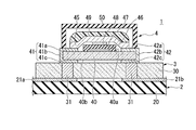
- FIG. 2 is a sectional view taken along line II-II in FIG. 1.
- FIG. 2 is a plan view showing a fuse element of the circuit module shown in FIG. 1 with a case omitted. It is a perspective view of the fuse element of the circuit module shown in FIG.
- FIG. 1 is a plan view of a circuit module according to an embodiment of the present invention.
- 2 is a sectional view taken along the line II-II of FIG. 1
- FIG. 3 is a plan view showing the fuse element shown in FIG. 1 with a case omitted
- FIG. 4 is a plan view of the fuse element shown in FIG. It is a perspective view.
- the circuit module 1 includes a circuit board 2, an insulating protection member 3 disposed on the circuit board, and a circuit board 2 with the insulating protection member 3 interposed therebetween. And a fuse element 4 mounted thereon.
- the fuse element 4 is arranged inside the outer periphery of the insulating protection member 3 in a plan view.
- the circuit board 2 has an insulating sheet 20 and wiring patterns 21a, 21b, 21c, 22 formed on the surface of the insulating sheet 20.
- the wiring patterns 21a, 21b, 21c are wiring patterns connected to the fuse element 4, and the wiring pattern 22 is a wiring pattern not connected to the fuse element 4.
- the insulating sheet 20 is not particularly limited as long as it has electrical insulating properties, and a known insulating sheet used for a circuit board such as a resin sheet, a ceramic sheet, or a composite sheet of resin and ceramic particles can be used. ..
- the resin sheet include an epoxy resin sheet, a phenol resin sheet, and a polyimide sheet.
- the ceramic sheet examples include an alumina sheet, a glass ceramic sheet, a mullite sheet, and a zirconia sheet.
- a glass epoxy sheet can be mentioned as an example of a composite sheet.
- the material of the wiring patterns 21a, 21b, 21c, 22 can be used a general electrode material such as Cu or Ag.
- the insulating protection member 3 has a function of protecting the wiring patterns 21a, 21b, 21c, 22 of the circuit board 2 from heat and arc emitted from the fuse element 4. Therefore, the outer circumference of the insulating protection member 3 is wider than the outer circumference of the fuse element 4.
- the distance between the outer circumference of the insulating protection member 3 and the outer circumference of the fuse element 4 varies depending on the size of the fuse element 4 and the usage conditions of the circuit module 1, but is generally within a range of 2 to 3 times the outer shape of the fuse element 4. Is preferred.
- the insulating protection member 3 is preferably flat. Although the thickness of the insulating protective member 3 varies depending on the heat resistance and thermal conductivity of the insulating protective member 3, it is generally preferable that the thickness is in the range of 100 ⁇ m to 1000 ⁇ m. Further, the outer periphery of the insulating protection member 3 may be raised in a wall shape.
- the insulating protection member 3 includes a non-conductive portion 30 and a conductive portion 31.
- the conductive portion 31 electrically connects the wiring patterns 21a, 21b, 21c of the circuit board 2 to the first electrode 41, the second electrode 42, and the first heating element electrode 43 of the fuse element 4.
- the non-conductive portion 30 is preferably made of a ceramic material having excellent heat resistance and thermal conductivity. Examples of ceramic materials include alumina, glass ceramics, mullite, and zirconia.
- a general electrode material such as Cu or Ag can be used.
- the form of the conductive portion 31 is a conductive through hole provided in the surface of the insulating protection member 3.
- the form of the conductive portion 31 is not particularly limited, and may be a conductive side through hole provided on the outer peripheral portion of the insulating protection member 3.
- the fuse element 4 has an insulating substrate 40.
- the insulating substrate 40 has a first electrode 41, a second electrode 42, a first heating element electrode 43, and a second heating element electrode 44 formed thereon.
- the first electrode 41 includes a first front surface electrode 41a formed on the front surface 40a of the insulating substrate 40, a first rear surface electrode 41c formed on the rear surface 40b of the insulating substrate 40, a first front surface electrode 41a and a first rear surface electrode. It is composed of a castellation 41b for connecting with 41c.
- the second electrode 42 includes a second front surface electrode 42a formed on the front surface 40a of the insulating substrate 40, a second rear surface electrode 42c formed on the rear surface 40b of the insulating substrate 40, a second front surface electrode 42a and a second rear surface electrode. It is composed of a castellation 42b for connecting with 42c.
- the first heating element electrode 43 includes a first heating element surface electrode 43a formed on the front surface 40a of the insulating substrate 40, a first heating element rear surface electrode (not shown) formed on the back surface 40b of the insulating substrate 40, and The first heating element front surface electrode 43a and the first heating element rear surface electrode (not shown) are connected to the castellation 43b.
- the second heating element electrode 44 is composed only of the second heating element surface electrode 44a formed on the surface 40a of the insulating substrate 40.
- a fusible conductor 45 that electrically cuts off the first surface electrode 41a and the second surface electrode 42a is electrically connected between the first surface electrode 41a and the second surface electrode 42a.
- the first back surface electrode 41c is the wiring pattern 21a
- the second back surface electrode 42c is the wiring pattern 21b
- the first heating element back surface electrode is the wiring pattern 21c, and electrically through the conductive portion 31 of the insulating protection member 3. It is connected.
- the wiring pattern 21c is electrically connected to an external control element (not shown), and a current is supplied to the first heating element electrode 43 by a signal from the control element.
- the surface 40 a of the insulating substrate 40 is provided with a heating element 46 and an insulating member 47 that covers the heating element 46.
- a heating element extraction electrode 48 is formed on the insulating member 47 so as to face the heating element 46.
- One end of the heating element 46 is electrically connected to the first heating element surface electrode 43a, and the other end is electrically connected to the second heating element surface electrode 44a.
- One end of the heating element lead-out electrode 48 is electrically connected to the second heating element surface electrode 44a and is also electrically connected to the fusible conductor 45.
- a flux 49 is applied to the surface of the fusible conductor 45 to prevent oxidation and improve wettability.
- the fuse element 4 includes a case 50 that covers the surface 40a of the insulating substrate 40.
- the case 50 has a side surface 51 bonded on the surface of the insulating substrate 40 and a top surface 53 that covers the surface of the insulating substrate 40.
- the case 50 has a through hole 52 only on the side surface 51.
- the number and size of the through holes 52 are not particularly limited, but it is preferable that one or more through holes 52 are provided on each of the four side surfaces 51 of the case 50.
- the case 50 is preferably made of a ceramic material having excellent heat resistance and thermal conductivity.
- ceramic materials include alumina, glass ceramics, mullite, and zirconia.
- the first electrode 41, the second electrode 42, the first heating element electrode 43, and the second heating element electrode 44 can be formed by using a general electrode material such as Cu or Ag. On the surfaces of the first electrode 41 and the second electrode 42, Ni/Au plating, Ni/Pd plating, Ni/Pd/Au plating, etc. are coated by a known method such as plating. It is preferable. Accordingly, it is possible to prevent the first electrode 41 and the second electrode 42 from being oxidized, and to prevent a change in rating due to an increase in conduction resistance.
- the fuse element 4 when the fuse element 4 is reflow-mounted, by melting the low melting point metal forming the connection solder or the outer layer of the fusible conductor 45, which connects the fusible conductor 45 with the first electrode 41 and the second electrode 42, It is possible to prevent the first electrode 41 and the second electrode 42 from being corroded (soldered).
- the fusible conductor 45 is made of a material that is quickly melted by self-heating (Joule heat) when overcurrent flows or by heat generation of the heating element 46.
- solder or Pb-free solder whose main component is Sn.
- Low melting point metals such as In and In can be preferably used.
- the fusible conductor 45 may be made of a high melting point metal such as Pb, Ag, Cu, or an alloy containing any one of these as a main component, or a laminated body of a low melting point metal and a high melting point metal. It may be.
- the fuse element 4 when the fuse element 4 is reflow mounted, even if the reflow temperature exceeds the melting temperature of the low melting point metal and the low melting point metal melts, Outflow to the outside can be suppressed and the shape of the soluble conductor 45 can be maintained. Also during melting, the low-melting point metal is melted and the high-melting point metal is eroded (soldered), so that the high-melting point metal can be rapidly melted at a temperature equal to or lower than the melting point.
- the heating element 46 is a conductive member that generates heat when energized, and has a high resistance such as W, Mo, Ru, Cu, Ag, or an alloy containing these as the main components or a composition or compound containing these. It is made of a conductive material.
- the heating element 46 is formed by a method in which a paste prepared by mixing a powder of a high resistance conductive material and a resin binder or the like is patterned on the insulating substrate 40 using a screen printing technique and then fired. You can
- the heating element lead-out electrode 48 has a function of transmitting the heat generated by the heating element 46 to the fusible conductor 45 via the second heating element surface electrode 44a.
- a material of the heating element extraction electrode 48 a metal material having high thermal conductivity such as Cu or Ag can be used.
- an insulating member may be interposed between the heating element 46 and the insulating substrate 40 in order to efficiently transfer the heat of the heating element 46 to the fusible conductor 45.
- the circuit module 1 of this embodiment can be manufactured, for example, as follows. First, the circuit board 2 having the wiring patterns 21a, 21b, and 21c at positions corresponding to the first electrode 41, the second electrode 42, and the first heating element electrode 43 of the fuse element 4, and the front side of the circuit board 2 of the fuse element 4 An insulating protection member 3 corresponding to the first electrode 41, the second electrode 42, and the first heating element electrode 43 and having a conductive portion 31 on the back surface side corresponding to the wiring patterns 21a, 21b, and 21c of the circuit board 2 is prepared.
- the insulating protection member 3 is mounted on the prepared circuit board 2, and solder is arranged between the wiring patterns 21a, 21b, 21c of the circuit board 2 and the conductive portion 31 of the insulating protection member 3.
- the fuse element 4 is mounted on the insulating protection member 3, and between the conductive portion 31 of the insulating protection member 3 and the first electrode 41, the second electrode 42, and the first heating element electrode 43 of the fuse element 4. Place the solder on.
- the solder is heated in the reflow furnace to insulate the wiring patterns 21a, 21b, 21c of the circuit board 2 from the first electrode 41, the second electrode 42, and the first heating element electrode 43 of the fuse element 4. It is electrically connected via the conductive portion 31 of the property protection member 3.
- the circuit module 1 of this embodiment can be used, for example, as a protection circuit for a battery pack of a lithium ion secondary battery.
- the circuit module 1 of the present embodiment is less likely to damage the periphery of the fuse element 4 even when an arc is generated in the fuse element 4, and thus is advantageously used as a protection circuit for a battery pack of an electric device that uses a large current. can do.
- an electric device using a large electric current an electric device using a large electric current exceeding several tens of amps to 100 A, for example, an electric tool such as an electric screwdriver, a transportation device such as a hybrid car, an electric vehicle, an electric assist bicycle Can be mentioned.
- the first heat generation is performed by a signal from an external control element (not shown).
- a current is supplied to the body electrode 43.
- the heating element 46 generates heat, and the heat is transmitted to the fusible conductor 45 via the second heating element surface electrode 44a and the heating element lead-out electrode 48, and the fusible conductor 45 is melted. Then, the current path in the circuit module 1 is cut off.
- the through hole 52 is formed in the side surface 51 of the case 50 of the fuse element 4, the heat generated when the fusible conductor 45 is melted, the air expanded by the heat, and the arc penetrate. It is discharged from the hole 52. Therefore, the case 50 is unlikely to be damaged when the fusible conductor 45 is melted.
- the fuse element 4 is arranged inside the outer periphery of the insulating protection member 3 in a plan view, and the surface of the circuit board 2 around the fuse element 4 is insulated. It is protected by the sex protection member 3. Therefore, even if heat or arc generated when the fusible conductor 45 of the fuse element 4 is blown is discharged to the outside through the through hole 52, the periphery of the fuse element 4 is unlikely to be damaged.
- the fuse element 4 connects the fusible conductor 45 between the first electrode 41 and the second electrode 42, but the number of electrodes is not limited as long as it is two or more.
- a pair of electrodes may be further provided, and another fusible conductor may be connected between the pair of electrodes.
- the through hole 52 is provided only on the side surface 51 of the case 50, but the through hole 52 may be provided on the top surface 53.
Landscapes
- Chemical & Material Sciences (AREA)
- Engineering & Computer Science (AREA)
- Combustion & Propulsion (AREA)
- Fuses (AREA)
- Non-Metallic Protective Coatings For Printed Circuits (AREA)
Abstract
Description
本願は、2019年2月14日に、日本に出願された特願2019-024470号に基づき優先権を主張し、その内容をここに援用する。
(3)上記(1)または(2)に記載の態様において、前記絶縁性保護部材は、前記ヒューズ素子の前記裏面電極と前記回路基板の前記配線パターンとを電気的に接続する導電部を備える構成としてよい。
(4)上記(3)に記載の態様において、前記導電部は、前記絶縁性保護部材の面内に設けられた導電性のスルーホール、または前記絶縁性保護部材の外周部に設けられた導電性のサイドスルーホールである構成としてもよい。
回路基板2は、絶縁シート20と、絶縁シート20の表面に形成された配線パターン21a、21b、21c、22とを有する。配線パターン21a、21b、21cはヒューズ素子4に接続する配線パターンであり、配線パターン22はヒューズ素子4に接続しない配線パターンである。絶縁シート20は電気絶縁性を有するものであれば特に制限はなく、樹脂シート、セラミックスシート、樹脂とセラミック粒子との複合体シートなど回路基板に用いられている公知の絶縁シートを用いることができる。樹脂シートの例としては、エポキシ樹脂シート、フェノール樹脂シート、ポリイミドシートを挙げることができる。セラミックスシートの例としては、アルミナシート、ガラスセラミックスシート、ムライトシート、ジルコニアシートを挙げることができる。複合体シートの例としては、ガラスエポキシシートを挙げることができる。配線パターン21a、21b、21c、22の材料としては、CuやAgなどの一般的な電極材料を用いることができる。
絶縁性保護部材3は、ヒューズ素子4から放出される熱やアークから回路基板2の配線パターン21a、21b、21c、22を保護する機能を有する。このため、絶縁性保護部材3の外周は、ヒューズ素子4の外周よりも広くなっている。絶縁性保護部材3の外周と、ヒューズ素子4の外周の距離は、ヒューズ素子4のサイズや回路モジュール1の使用条件によって異なるが、一般に、ヒューズ素子4の外形の2倍~3倍の範囲内にあることが好ましい。
ヒューズ素子4は、絶縁基板40を有する。絶縁基板40は、第1電極41、第2電極42、第1発熱体電極43、第2発熱体電極44が形成されている。第1電極41は、絶縁基板40の表面40aに形成された第1表面電極41aと、絶縁基板40の裏面40bに形成された第1裏面電極41cと、第1表面電極41aと第1裏面電極41cとを接続するキャスタレーション41bとからなる。第2電極42は、絶縁基板40の表面40aに形成された第2表面電極42aと、絶縁基板40の裏面40bに形成された第2裏面電極42cと、第2表面電極42aと第2裏面電極42cとを接続するキャスタレーション42bとからなる。第1発熱体電極43は、絶縁基板40の表面40aに形成された第1発熱体表面電極43aと、絶縁基板40の裏面40bに形成された第1発熱体裏面電極(不図示)と、第1発熱体表面電極43aと第1発熱体裏面電極(不図示)とを接続するキャスタレーション43bとからなる。第2発熱体電極44は、絶縁基板40の表面40aに形成された第2発熱体表面電極44aのみからなる。
発熱体引出電極48は、発熱体46にて発生した熱を、第2発熱体表面電極44aを介して、可溶導体45に伝える機能を有する。発熱体引出電極48の材料としては、CuやAgなどの熱伝導性が高い金属材料を用いることができる。また、発熱体46の熱を効率良く可溶導体45に伝えるために、発熱体46と絶縁基板40の間に絶縁部材を介在させてもよい。
まず始めに、ヒューズ素子4の第1電極41、第2電極42、第1発熱体電極43に対応する位置に配線パターン21a、21b、21cを有する回路基板2と、表面側がヒューズ素子4の第1電極41、第2電極42、第1発熱体電極43と対応し、裏面側が回路基板2の配線パターン21a、21b、21cと対応する導電部31を有する絶縁性保護部材3とを用意する。
本実施形態では、ヒューズ素子4は、第1電極41と第2電極42との間に可溶導体45を接続しているが、電極の個数は2個以上の複数個であれば制限ない。例えば、さらに一対の電極を設けて、その一対の電極の間に別の可溶導体を接続してもよい。
また、本実施形態では、ケース50の側面51にのみ貫通孔52が設けられているが、貫通孔52は天面53に設けてもよい。
2 回路基板
3 絶縁性保護部材
4 ヒューズ素子
20 絶縁シート
21a、21b、21c、22 配線パターン
30 非導電部
31 導電部
40 絶縁基板
40a 表面
40b 裏面
41 第1電極
41a 第1表面電極
41b キャスタレーション
41c 第1裏面電極
42 第2電極
42a 第2表面電極
42b キャスタレーション
42c 第2裏面電極
43 第1発熱体電極
43a 第1発熱体表面電極
43b キャスタレーション
44 第2発熱体電極
44a 第2発熱体表面電極
45 可溶導体
46 発熱体
47 絶縁部材
48 発熱体引出電極
49 フラックス
50 ケース
51 側面
52 貫通孔
53 天面
Claims (4)
- 配線パターンを有する回路基板と、
前記回路基板の上に配置された絶縁性保護部材と、
前記絶縁性保護部材を介して前記回路基板の上に実装されたヒューズ素子とを備え、
前記ヒューズ素子は、
絶縁基板と、
前記絶縁基板の表面に形成された複数の表面電極と、
前記複数の表面電極間に接続され、溶断することにより前記複数の表面電極間を遮断する可溶導体と、
前記絶縁基板の裏面に形成され、前記複数の表面電極と電気的に接続された複数の裏面電極と、
前記絶縁基板の表面を覆うケースとを備え、
前記ケースは側面または天面に貫通孔を有し、
前記ヒューズ素子は平面視したときに前記絶縁性保護部材の外周よりも内側に配置されている回路モジュール。 - 前記絶縁性保護部材は、平板状である請求項1に記載の回路モジュール。
- 前記絶縁性保護部材は、前記ヒューズ素子の前記裏面電極と前記回路基板の前記配線パターンとを電気的に接続する導電部を備える請求項1または2に記載の回路モジュール。
- 前記導電部は、前記絶縁性保護部材の面内に設けられた導電性のスルーホール、または前記絶縁性保護部材の外周部に設けられた導電性のサイドスルーホールである請求項3に記載の回路モジュール。
Priority Applications (3)
| Application Number | Priority Date | Filing Date | Title |
|---|---|---|---|
| KR1020217024514A KR20210105995A (ko) | 2019-02-14 | 2020-02-05 | 회로 모듈 |
| KR1020247021465A KR20240105509A (ko) | 2019-02-14 | 2020-02-05 | 회로 모듈 |
| CN202080012774.XA CN113424289A (zh) | 2019-02-14 | 2020-02-05 | 电路模块 |
Applications Claiming Priority (2)
| Application Number | Priority Date | Filing Date | Title |
|---|---|---|---|
| JP2019-024470 | 2019-02-14 | ||
| JP2019024470A JP2020135959A (ja) | 2019-02-14 | 2019-02-14 | 回路モジュール |
Publications (1)
| Publication Number | Publication Date |
|---|---|
| WO2020166445A1 true WO2020166445A1 (ja) | 2020-08-20 |
Family
ID=72044728
Family Applications (1)
| Application Number | Title | Priority Date | Filing Date |
|---|---|---|---|
| PCT/JP2020/004325 Ceased WO2020166445A1 (ja) | 2019-02-14 | 2020-02-05 | 回路モジュール |
Country Status (5)
| Country | Link |
|---|---|
| JP (2) | JP2020135959A (ja) |
| KR (2) | KR20240105509A (ja) |
| CN (1) | CN113424289A (ja) |
| TW (1) | TW202036632A (ja) |
| WO (1) | WO2020166445A1 (ja) |
Citations (3)
| Publication number | Priority date | Publication date | Assignee | Title |
|---|---|---|---|---|
| JP2006185951A (ja) * | 2004-12-24 | 2006-07-13 | Sumitomo Wiring Syst Ltd | 回路基板への基板用端子の取付構造 |
| JP2010272215A (ja) * | 2009-05-19 | 2010-12-02 | Panasonic Corp | 電池ユニット |
| JP2016134317A (ja) * | 2015-01-20 | 2016-07-25 | デクセリアルズ株式会社 | ヒューズ素子及び回路モジュール |
Family Cites Families (1)
| Publication number | Priority date | Publication date | Assignee | Title |
|---|---|---|---|---|
| JP6782122B2 (ja) * | 2016-08-24 | 2020-11-11 | デクセリアルズ株式会社 | 保護素子、回路モジュール及び保護素子の製造方法 |
-
2019
- 2019-02-14 JP JP2019024470A patent/JP2020135959A/ja active Pending
-
2020
- 2020-02-05 KR KR1020247021465A patent/KR20240105509A/ko not_active Ceased
- 2020-02-05 KR KR1020217024514A patent/KR20210105995A/ko not_active Ceased
- 2020-02-05 WO PCT/JP2020/004325 patent/WO2020166445A1/ja not_active Ceased
- 2020-02-05 CN CN202080012774.XA patent/CN113424289A/zh active Pending
- 2020-02-06 TW TW109103658A patent/TW202036632A/zh unknown
-
2023
- 2023-07-06 JP JP2023111785A patent/JP2023126322A/ja active Pending
Patent Citations (3)
| Publication number | Priority date | Publication date | Assignee | Title |
|---|---|---|---|---|
| JP2006185951A (ja) * | 2004-12-24 | 2006-07-13 | Sumitomo Wiring Syst Ltd | 回路基板への基板用端子の取付構造 |
| JP2010272215A (ja) * | 2009-05-19 | 2010-12-02 | Panasonic Corp | 電池ユニット |
| JP2016134317A (ja) * | 2015-01-20 | 2016-07-25 | デクセリアルズ株式会社 | ヒューズ素子及び回路モジュール |
Also Published As
| Publication number | Publication date |
|---|---|
| JP2020135959A (ja) | 2020-08-31 |
| CN113424289A (zh) | 2021-09-21 |
| JP2023126322A (ja) | 2023-09-07 |
| KR20240105509A (ko) | 2024-07-05 |
| KR20210105995A (ko) | 2021-08-27 |
| TW202036632A (zh) | 2020-10-01 |
Similar Documents
| Publication | Publication Date | Title |
|---|---|---|
| JP6437253B2 (ja) | 保護素子及び実装体 | |
| JP6437262B2 (ja) | 実装体の製造方法、温度ヒューズ素子の実装方法及び温度ヒューズ素子 | |
| JP6576618B2 (ja) | 保護素子 | |
| TWI389159B (zh) | Protection element | |
| JP6580504B2 (ja) | 保護素子 | |
| CN108475602B (zh) | 熔丝元件 | |
| JP6707377B2 (ja) | 保護素子 | |
| WO2016117578A1 (ja) | ヒューズ素子及び回路モジュール | |
| TW201830446A (zh) | 保護元件 | |
| TWI629702B (zh) | Blocking element and blocking element circuit | |
| JP4663758B2 (ja) | 抵抗付き温度ヒューズ及び電池保護回路板 | |
| JP6801974B2 (ja) | 保護素子 | |
| JP2015230804A (ja) | 短絡素子 | |
| CN110741457A (zh) | 保护元件 | |
| JP2018018835A (ja) | 保護素子、ヒューズ素子 | |
| JP6231323B2 (ja) | 保護素子、及びこれを用いた保護回路基板 | |
| TWI685870B (zh) | 短路元件 | |
| JP2023126322A (ja) | 回路モジュール | |
| WO2017104597A1 (ja) | ヒューズ素子 | |
| JP6959964B2 (ja) | 保護素子 | |
| WO2023167069A1 (ja) | 保護素子 | |
| CN118541771A (zh) | 保护器件以及电池包 | |
| JP2000182493A (ja) | 回路用保護素子 |
Legal Events
| Date | Code | Title | Description |
|---|---|---|---|
| 121 | Ep: the epo has been informed by wipo that ep was designated in this application |
Ref document number: 20755217 Country of ref document: EP Kind code of ref document: A1 |
|
| ENP | Entry into the national phase |
Ref document number: 20217024514 Country of ref document: KR Kind code of ref document: A |
|
| NENP | Non-entry into the national phase |
Ref country code: DE |
|
| 122 | Ep: pct application non-entry in european phase |
Ref document number: 20755217 Country of ref document: EP Kind code of ref document: A1 |
|
| WWR | Wipo information: refused in national office |
Ref document number: 1020247021465 Country of ref document: KR |