WO2020162412A1 - フィルム状接着剤、接着シート、及び半導体装置 - Google Patents
フィルム状接着剤、接着シート、及び半導体装置 Download PDFInfo
- Publication number
- WO2020162412A1 WO2020162412A1 PCT/JP2020/003972 JP2020003972W WO2020162412A1 WO 2020162412 A1 WO2020162412 A1 WO 2020162412A1 JP 2020003972 W JP2020003972 W JP 2020003972W WO 2020162412 A1 WO2020162412 A1 WO 2020162412A1
- Authority
- WO
- WIPO (PCT)
- Prior art keywords
- adhesive
- film
- semiconductor element
- semiconductor
- semiconductor device
- Prior art date
- Legal status (The legal status is an assumption and is not a legal conclusion. Google has not performed a legal analysis and makes no representation as to the accuracy of the status listed.)
- Ceased
Links
Images


Classifications
-
- C—CHEMISTRY; METALLURGY
- C09—DYES; PAINTS; POLISHES; NATURAL RESINS; ADHESIVES; COMPOSITIONS NOT OTHERWISE PROVIDED FOR; APPLICATIONS OF MATERIALS NOT OTHERWISE PROVIDED FOR
- C09J—ADHESIVES; NON-MECHANICAL ASPECTS OF ADHESIVE PROCESSES IN GENERAL; ADHESIVE PROCESSES NOT PROVIDED FOR ELSEWHERE; USE OF MATERIALS AS ADHESIVES
- C09J7/00—Adhesives in the form of films or foils
- C09J7/30—Adhesives in the form of films or foils characterised by the adhesive composition
-
- C—CHEMISTRY; METALLURGY
- C09—DYES; PAINTS; POLISHES; NATURAL RESINS; ADHESIVES; COMPOSITIONS NOT OTHERWISE PROVIDED FOR; APPLICATIONS OF MATERIALS NOT OTHERWISE PROVIDED FOR
- C09J—ADHESIVES; NON-MECHANICAL ASPECTS OF ADHESIVE PROCESSES IN GENERAL; ADHESIVE PROCESSES NOT PROVIDED FOR ELSEWHERE; USE OF MATERIALS AS ADHESIVES
- C09J119/00—Adhesives based on rubbers, not provided for in groups C09J107/00 - C09J117/00
-
- C—CHEMISTRY; METALLURGY
- C09—DYES; PAINTS; POLISHES; NATURAL RESINS; ADHESIVES; COMPOSITIONS NOT OTHERWISE PROVIDED FOR; APPLICATIONS OF MATERIALS NOT OTHERWISE PROVIDED FOR
- C09J—ADHESIVES; NON-MECHANICAL ASPECTS OF ADHESIVE PROCESSES IN GENERAL; ADHESIVE PROCESSES NOT PROVIDED FOR ELSEWHERE; USE OF MATERIALS AS ADHESIVES
- C09J133/00—Adhesives based on homopolymers or copolymers of compounds having one or more unsaturated aliphatic radicals, each having only one carbon-to-carbon double bond, and at least one being terminated by only one carboxyl radical, or of salts, anhydrides, esters, amides, imides, or nitriles thereof; Adhesives based on derivatives of such polymers
- C09J133/04—Homopolymers or copolymers of esters
-
- C—CHEMISTRY; METALLURGY
- C09—DYES; PAINTS; POLISHES; NATURAL RESINS; ADHESIVES; COMPOSITIONS NOT OTHERWISE PROVIDED FOR; APPLICATIONS OF MATERIALS NOT OTHERWISE PROVIDED FOR
- C09J—ADHESIVES; NON-MECHANICAL ASPECTS OF ADHESIVE PROCESSES IN GENERAL; ADHESIVE PROCESSES NOT PROVIDED FOR ELSEWHERE; USE OF MATERIALS AS ADHESIVES
- C09J133/00—Adhesives based on homopolymers or copolymers of compounds having one or more unsaturated aliphatic radicals, each having only one carbon-to-carbon double bond, and at least one being terminated by only one carboxyl radical, or of salts, anhydrides, esters, amides, imides, or nitriles thereof; Adhesives based on derivatives of such polymers
- C09J133/18—Homopolymers or copolymers of nitriles
- C09J133/20—Homopolymers or copolymers of acrylonitrile
-
- C—CHEMISTRY; METALLURGY
- C09—DYES; PAINTS; POLISHES; NATURAL RESINS; ADHESIVES; COMPOSITIONS NOT OTHERWISE PROVIDED FOR; APPLICATIONS OF MATERIALS NOT OTHERWISE PROVIDED FOR
- C09J—ADHESIVES; NON-MECHANICAL ASPECTS OF ADHESIVE PROCESSES IN GENERAL; ADHESIVE PROCESSES NOT PROVIDED FOR ELSEWHERE; USE OF MATERIALS AS ADHESIVES
- C09J7/00—Adhesives in the form of films or foils
- C09J7/20—Adhesives in the form of films or foils characterised by their carriers
-
- C—CHEMISTRY; METALLURGY
- C09—DYES; PAINTS; POLISHES; NATURAL RESINS; ADHESIVES; COMPOSITIONS NOT OTHERWISE PROVIDED FOR; APPLICATIONS OF MATERIALS NOT OTHERWISE PROVIDED FOR
- C09J—ADHESIVES; NON-MECHANICAL ASPECTS OF ADHESIVE PROCESSES IN GENERAL; ADHESIVE PROCESSES NOT PROVIDED FOR ELSEWHERE; USE OF MATERIALS AS ADHESIVES
- C09J7/00—Adhesives in the form of films or foils
- C09J7/30—Adhesives in the form of films or foils characterised by the adhesive composition
- C09J7/38—Pressure-sensitive adhesives [PSA]
-
- H—ELECTRICITY
- H10—SEMICONDUCTOR DEVICES; ELECTRIC SOLID-STATE DEVICES NOT OTHERWISE PROVIDED FOR
- H10W—GENERIC PACKAGES, INTERCONNECTIONS, CONNECTORS OR OTHER CONSTRUCTIONAL DETAILS OF DEVICES COVERED BY CLASS H10
- H10W72/00—Interconnections or connectors in packages
- H10W72/071—Connecting or disconnecting
-
- C—CHEMISTRY; METALLURGY
- C09—DYES; PAINTS; POLISHES; NATURAL RESINS; ADHESIVES; COMPOSITIONS NOT OTHERWISE PROVIDED FOR; APPLICATIONS OF MATERIALS NOT OTHERWISE PROVIDED FOR
- C09J—ADHESIVES; NON-MECHANICAL ASPECTS OF ADHESIVE PROCESSES IN GENERAL; ADHESIVE PROCESSES NOT PROVIDED FOR ELSEWHERE; USE OF MATERIALS AS ADHESIVES
- C09J2203/00—Applications of adhesives in processes or use of adhesives in the form of films or foils
- C09J2203/326—Applications of adhesives in processes or use of adhesives in the form of films or foils for bonding electronic components such as wafers, chips or semiconductors
-
- H—ELECTRICITY
- H10—SEMICONDUCTOR DEVICES; ELECTRIC SOLID-STATE DEVICES NOT OTHERWISE PROVIDED FOR
- H10W—GENERIC PACKAGES, INTERCONNECTIONS, CONNECTORS OR OTHER CONSTRUCTIONAL DETAILS OF DEVICES COVERED BY CLASS H10
- H10W72/00—Interconnections or connectors in packages
- H10W72/851—Dispositions of multiple connectors or interconnections
- H10W72/874—On different surfaces
- H10W72/884—Die-attach connectors and bond wires
-
- H—ELECTRICITY
- H10—SEMICONDUCTOR DEVICES; ELECTRIC SOLID-STATE DEVICES NOT OTHERWISE PROVIDED FOR
- H10W—GENERIC PACKAGES, INTERCONNECTIONS, CONNECTORS OR OTHER CONSTRUCTIONAL DETAILS OF DEVICES COVERED BY CLASS H10
- H10W74/00—Encapsulations, e.g. protective coatings
-
- H—ELECTRICITY
- H10—SEMICONDUCTOR DEVICES; ELECTRIC SOLID-STATE DEVICES NOT OTHERWISE PROVIDED FOR
- H10W—GENERIC PACKAGES, INTERCONNECTIONS, CONNECTORS OR OTHER CONSTRUCTIONAL DETAILS OF DEVICES COVERED BY CLASS H10
- H10W90/00—Package configurations
- H10W90/701—Package configurations characterised by the relative positions of pads or connectors relative to package parts
- H10W90/731—Package configurations characterised by the relative positions of pads or connectors relative to package parts of die-attach connectors
- H10W90/732—Package configurations characterised by the relative positions of pads or connectors relative to package parts of die-attach connectors between stacked chips
-
- H—ELECTRICITY
- H10—SEMICONDUCTOR DEVICES; ELECTRIC SOLID-STATE DEVICES NOT OTHERWISE PROVIDED FOR
- H10W—GENERIC PACKAGES, INTERCONNECTIONS, CONNECTORS OR OTHER CONSTRUCTIONAL DETAILS OF DEVICES COVERED BY CLASS H10
- H10W90/00—Package configurations
- H10W90/701—Package configurations characterised by the relative positions of pads or connectors relative to package parts
- H10W90/731—Package configurations characterised by the relative positions of pads or connectors relative to package parts of die-attach connectors
- H10W90/734—Package configurations characterised by the relative positions of pads or connectors relative to package parts of die-attach connectors between a chip and a stacked insulating package substrate, interposer or RDL
-
- H—ELECTRICITY
- H10—SEMICONDUCTOR DEVICES; ELECTRIC SOLID-STATE DEVICES NOT OTHERWISE PROVIDED FOR
- H10W—GENERIC PACKAGES, INTERCONNECTIONS, CONNECTORS OR OTHER CONSTRUCTIONAL DETAILS OF DEVICES COVERED BY CLASS H10
- H10W90/00—Package configurations
- H10W90/701—Package configurations characterised by the relative positions of pads or connectors relative to package parts
- H10W90/751—Package configurations characterised by the relative positions of pads or connectors relative to package parts of bond wires
- H10W90/754—Package configurations characterised by the relative positions of pads or connectors relative to package parts of bond wires between a chip and a stacked insulating package substrate, interposer or RDL
Definitions
- the present invention relates to a film adhesive, an adhesive sheet, and a semiconductor device.
- stacked MCPs Multi Chip Packages
- semiconductor elements semiconductor elements (semiconductor chips) are stacked in multiple stages
- memory semiconductor packages for mobile phones and mobile audio devices.
- higher speed, higher density, and higher integration of semiconductor packages are being promoted.
- the speed has been increased by using copper as a wiring material for semiconductor chip circuits.
- lead frames and the like made of copper are being used from the viewpoint of improving the reliability of connection to a complicated mounting board and accelerating the exhaust heat from the semiconductor package.
- the semiconductor package has an electrical characteristic. Tends to be difficult to secure. In particular, in a semiconductor package in which semiconductor chips are laminated in multiple stages, copper ions generated by corrosion move inside the adhesive, and electrical signal loss tends to occur within the semiconductor chips or between semiconductor chips/semiconductor chips.
- Adhesives that capture copper ions generated in semiconductor packages are being studied from the viewpoint of preventing loss of electrical signals.
- a thermoplastic resin having an epoxy group and not having a carboxyl group and a heterocyclic compound containing a tertiary nitrogen atom as a ring atom are formed, and a complex is formed with a cation.
- An adhesive sheet for manufacturing a semiconductor device having an organic complex forming compound is disclosed.
- the main object of the present invention is to provide a film-like adhesive capable of sufficiently suppressing the problems associated with the movement of copper ions in the adhesive.
- One aspect of the present invention is a film adhesive for adhering a semiconductor element and a supporting member on which the semiconductor element is mounted, which contains acrylic rubber, the acrylic rubber being the following condition (i) or condition (ii).
- the film adhesive which satisfy
- Another aspect of the present invention provides an adhesive sheet including a base material and the above-mentioned film adhesive provided on one surface of the base material.
- the substrate may be a dicing tape.
- Another aspect of the present invention includes a semiconductor element, a support member on which the semiconductor element is mounted, and an adhesive member provided between the semiconductor element and the support member for adhering the semiconductor element and the support member to each other.
- an adhesive member provided between the semiconductor element and the support member for adhering the semiconductor element and the support member to each other.
- a film-like adhesive capable of sufficiently suppressing a defect due to movement of copper ions in the adhesive. Further, according to the present invention, an adhesive sheet and a semiconductor device using such a film adhesive are provided.
- the numerical range indicated by “to” indicates a range including the numerical values before and after “to” as the minimum value and the maximum value, respectively.
- the upper limit value or the lower limit value described in one numerical range may be replaced with the upper limit value or the lower limit value of another stepwise described numerical range.
- the upper limit value or the lower limit value of the numerical range may be replaced with the value shown in the examples.
- the (meth)acrylic acid ester means an acrylic acid ester or a corresponding methacrylic acid ester.
- the film adhesive according to one embodiment is a film adhesive for adhering a semiconductor element and a supporting member on which the semiconductor element is mounted, and the film adhesive is an acrylic rubber (hereinafter, referred to as “(A) In some cases, it is referred to as "ingredient”.
- the film adhesive can be obtained by molding an adhesive composition containing the component (A) into a film.
- the film adhesive and the adhesive composition may be in a semi-cured (B stage) state.
- the component (A) is a rubber having a structural unit derived from a (meth)acrylic acid ester as a main component.
- the content of the structural unit derived from the (meth)acrylic acid ester in the component (A) may be, for example, 70% by mass or more, 80% by mass or more, or 90% by mass or more based on the total amount of the structural unit.
- the component (A) may include a constituent unit derived from a (meth)acrylic acid ester having a crosslinkable functional group such as an epoxy group, an alcoholic or phenolic hydroxyl group, and a carboxyl group.
- condition (i) It has a structural unit derived from acrylonitrile and has a glass transition temperature (Tg) of more than 12°C.
- condition (ii) It has no structural unit derived from acrylonitrile and has a glass transition temperature (Tg) of 0° C. or higher.
- the glass transition temperature (Tg) of the component (A) is more than 12°C and 55°C or less, 15°C or more and 30°C or less, Alternatively, it may be 19° C. or higher and 25° C. or lower.
- the condition (ii) when the component (A) does not have a structural unit derived from acrylonitrile, it may be 0°C or higher and 50°C or lower, 10°C or higher and 30°C or lower, or 15°C or higher and 25°C or lower.
- the glass transition temperature (Tg) means a value measured by using a DSC (Thermal Differential Scanning Calorimeter) (for example, Thermo Plus 2 manufactured by Rigaku Corporation).
- the glass transition temperature (Tg) of the component (A) is adjusted within a predetermined range, for example, by adjusting the ratio of the (meth)acrylic acid ester having a high Tg and the (meth)acrylic acid ester having a low Tg. can do.
- Examples of commercially available products of the component (A) having a structural unit derived from acrylonitrile include SG-P3, SG-80H, HTR-860P-3CSP (all manufactured by Nagase Chemtex Co., Ltd.) and the like.
- Examples of commercially available products of the component (A) having no structural unit derived from acrylonitrile include KH-CT-865 (manufactured by Hitachi Chemical Co., Ltd.).
- the film adhesive may be composed of the component (A), but may further contain other components.
- other components include pigments, ion trapping agents, antioxidants and the like.
- the content of the other components may be 0 to 30 parts by mass based on 100 parts by mass of the total amount of the component (A).
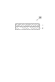
- FIG. 1 is a schematic cross-sectional view showing an embodiment of a film adhesive.
- the film adhesive 1 (adhesive film) shown in FIG. 1 is obtained by molding an adhesive composition into a film.
- the film adhesive 1 may be in a semi-cured (B stage) state.
- Such a film adhesive 1 can be formed by applying an adhesive composition to a support film.
- the varnish of the adhesive composition adheresive varnish
- the component (A) and other components added as necessary are mixed in a solvent, and the mixed liquid is mixed or kneaded to form the adhesive varnish.
- the film adhesive 1 can be formed by preparing, applying the adhesive varnish on the support film, and heating and drying the solvent to remove.
- the support film is not particularly limited as long as it can withstand the above heat drying, for example, polyester film, polypropylene film, polyethylene terephthalate film, polyimide film, polyetherimide film, polyether naphthalate film, polymethylpentene film, etc. May be
- the support film may be a multilayer film in which two or more kinds are combined, and the surface thereof may be treated with a release agent such as a silicone-based or silica-based release agent.
- the thickness of the support film may be, for example, 1 to 200 ⁇ m or 5 to 170 ⁇ m.
- the mixing or kneading can be performed by using an ordinary agitator, a raider, a three-roller, a ball mill, or other disperser, and appropriately combining these.
- the solvent used for preparing the adhesive varnish is not limited as long as it can uniformly dissolve, knead, or disperse each component, and conventionally known solvents can be used.
- a solvent include ketone solvents such as acetone, methyl ethyl ketone, methyl isobutyl ketone and cyclohexanone, dimethylformamide, dimethylacetamide, N-methyl-2-pyrrolidone, toluene and xylene.
- the solvent may be methyl ethyl ketone, cyclohexanone or the like because of its high drying rate and low price.
- a known method can be used, and examples thereof include a knife coating method, a roll coating method, a spray coating method, a gravure coating method, a bar coating method, and a curtain coating method.
- the heating and drying conditions are not particularly limited as long as the solvent used is sufficiently volatilized, but heating and drying can be performed at 50 to 150° C. for 1 to 30 minutes.
- the thickness of the film adhesive may be 50 ⁇ m or less.
- the thickness of the film-like adhesive is 50 ⁇ m or less, the distance between the semiconductor element and the supporting member mounting the semiconductor element becomes short, so that defects due to copper ions tend to occur easily. Since the film adhesive according to the present embodiment can sufficiently suppress the movement (permeation) of copper ions in the adhesive, the thickness thereof can be 50 ⁇ m or less.
- the thickness of the film adhesive 1 may be 40 ⁇ m or less, 30 ⁇ m or less, 20 ⁇ m or less, or 10 ⁇ m or less.
- the lower limit of the thickness of the film adhesive 1 is not particularly limited, but may be 1 ⁇ m or more, for example.
- the copper ion permeation time of the film adhesive in the semi-cured (B stage) state may be more than 250 minutes, and may be 300 minutes or more, 350 minutes or more, or 400 minutes or more.
- the copper ion permeation time is more than 250 minutes, it is expected that even if a defect such as insufficient curing occurs during manufacturing of the semiconductor device, a defect due to copper ions is less likely to occur.
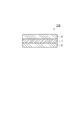
- FIG. 2 is a schematic cross-sectional view showing an embodiment of the adhesive sheet.
- the adhesive sheet 100 shown in FIG. 2 includes a base material 2 and a film adhesive 1 provided on the base material 2.
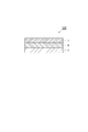
- FIG. 3 is a schematic cross-sectional view showing another embodiment of the adhesive sheet.
- the adhesive sheet 110 shown in FIG. 3 includes a base material 2, a film adhesive 1 provided on the base material 2, and a cover film provided on the surface of the film adhesive 1 opposite to the base material 2. 3 and 3.
- the base material 2 is not particularly limited, but may be a base material film.
- the base film may be similar to the support film described above.
- the cover film 3 is used to prevent damage or contamination of the film adhesive, and may be, for example, a polyethylene film, a polypropylene film, a surface release agent treated film, or the like.
- the thickness of the cover film 3 may be, for example, 15 to 200 ⁇ m or 70 to 170 ⁇ m.
- the adhesive sheets 100 and 110 can be formed by applying an adhesive composition to a base film, similar to the method of forming the film adhesive described above.
- the method of applying the adhesive composition to the substrate 2 may be the same as the method of applying the adhesive composition to the support film.
- the adhesive sheet 110 can be obtained by further laminating the cover film 3 on the film adhesive 1.
- the adhesive sheets 100 and 110 may be formed by using a film-shaped adhesive agent prepared in advance.
- the adhesive sheet 100 can be formed by laminating under a predetermined condition (for example, room temperature (20° C.) or a heated state) using a roll laminator, a vacuum laminator, or the like. Since the adhesive sheet 100 can be continuously manufactured and is excellent in efficiency, it may be formed using a roll laminator in a heated state.
- the adhesive sheet is a dicing/die bonding integrated adhesive sheet in which the base material 2 is a dicing tape.
- the process of laminating on the semiconductor wafer is performed once, so that the work efficiency can be improved.
- the dicing tape examples include plastic films such as polytetrafluoroethylene film, polyethylene terephthalate film, polyethylene film, polypropylene film, polymethylpentene film and polyimide film. Further, the dicing tape may be subjected to surface treatment such as primer coating, UV treatment, corona discharge treatment, polishing treatment and etching treatment, if necessary.
- the dicing tape may have adhesiveness. Such a dicing tape may be one in which the above-mentioned plastic film is provided with adhesiveness, or one in which the above-mentioned plastic film is provided with an adhesive layer.
- the pressure-sensitive adhesive layer may be either a pressure-sensitive type or a radiation-curable type, has a sufficient adhesive force so that the semiconductor element does not scatter during dicing, and does not damage the semiconductor element in the subsequent semiconductor element pickup step.
- a pressure-sensitive type or a radiation-curable type
- has a sufficient adhesive force so that the semiconductor element does not scatter during dicing, and does not damage the semiconductor element in the subsequent semiconductor element pickup step.
- the thickness of the dicing tape may be 60 to 150 ⁇ m or 70 to 130 ⁇ m from the viewpoints of economy and handleability of the film.
- FIG. 4 is a schematic cross-sectional view showing another embodiment of the adhesive sheet.
- FIG. 5 is a schematic cross-sectional view showing another embodiment of the adhesive sheet.
- the adhesive sheet 120 shown in FIG. 4 includes the dicing tape 7, the pressure-sensitive adhesive layer 6, and the film adhesive 1 in this order.
- the adhesive sheet 130 shown in FIG. 5 includes the dicing tape 7 and the film adhesive 1 provided on the dicing tape 7.
- the adhesive sheet 120 can be obtained, for example, by providing the pressure-sensitive adhesive layer 6 on the dicing tape 7 and further laminating the film adhesive 1 on the pressure-sensitive adhesive layer 6.
- the adhesive sheet 130 can be obtained, for example, by bonding the dicing tape 7 and the film adhesive 1 together.
- the film-like adhesive and the adhesive sheet may be used for manufacturing a semiconductor device, and the film-like adhesive and the dicing tape are applied to a semiconductor wafer or a semiconductor element (semiconductor chip) which has already been diced at 0° C. After pasting at ⁇ 90°C, the film-shaped adhesive-attached semiconductor element is obtained by cutting with a rotary blade, laser or stretching, and then the film-shaped adhesive-attached semiconductor element is applied to an organic substrate, a lead frame, or another semiconductor. It may be used for manufacturing a semiconductor device including a step of adhering on an element.
- semiconductor wafers include single crystal silicon, polycrystalline silicon, various ceramics, and compound semiconductors such as gallium arsenide.
- the film adhesive and the adhesive sheet include semiconductor elements such as IC and LSI, lead frames such as 42 alloy lead frame and copper lead frame; plastic films such as polyimide resin and epoxy resin; It can be used as an adhesive for die bonding for bonding a material impregnated and cured with a plastic such as an epoxy resin; a support member for mounting a semiconductor made of ceramics such as alumina.
- the film adhesive and the adhesive sheet are also suitably used as an adhesive for adhering semiconductor elements to each other in a Stacked-PKG having a structure in which a plurality of semiconductor elements are stacked.
- one semiconductor element serves as a support member on which the semiconductor element is mounted.
- the film adhesive and the adhesive sheet are, for example, a protective sheet for protecting the back surface of the semiconductor element of the flip-chip type semiconductor device, and a material for sealing between the surface of the semiconductor element of the flip-chip type semiconductor device and the adherend. It can also be used as a sealing sheet or the like.
- a semiconductor device manufactured using a film adhesive will be specifically described with reference to the drawings.
- semiconductor devices having various structures have been proposed, and the application of the film adhesive according to the present embodiment is not limited to the semiconductor device having the structure described below.
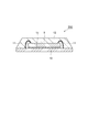
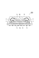
- FIG. 6 is a schematic sectional view showing an embodiment of a semiconductor device.
- the semiconductor device 200 shown in FIG. 6 is provided between the semiconductor element 9, the support member 10 on which the semiconductor element 9 is mounted, and the semiconductor element 9 and the support member 10, and is bonded to bond the semiconductor element 9 and the support member 10.
- the member 1c (film adhesive or cured product thereof).
- the adhesive member 1c is a film adhesive or a cured product thereof.
- a connection terminal (not shown) of the semiconductor element 9 is electrically connected to an external connection terminal (not shown) via a wire 11 and sealed by a sealing material 12.
- FIG. 7 is a schematic cross-sectional view showing another embodiment of the semiconductor device.
- the semiconductor element 9a in the first stage is adhered to the supporting member 10 on which the terminals 13 are formed by the adhesive member 1c, and the semiconductor element 9a in the second stage is further attached to the supporting member 10 in the second stage by the adhesive member 1c.
- the eye semiconductor element 9b is adhered.
- the connection terminals (not shown) of the semiconductor element 9 a in the first stage and the semiconductor element 9 b in the second stage are electrically connected to the external connection terminals via the wires 11 and sealed by the sealing material 12.
- the adhesive member 1c is a film adhesive or a cured product thereof. As described above, the film adhesive according to the present embodiment can be suitably used for a semiconductor device having a structure in which a plurality of semiconductor elements are stacked.
- the semiconductor device (semiconductor package) shown in FIGS. 6 and 7 has, for example, a film adhesive interposed between a semiconductor element and a support member or between semiconductor elements and heated and pressure-bonded to each other. Are bonded, and then, if necessary, a wire bonding step, a sealing step with a sealing material, a heating and melting step including reflow with solder, and the like.
- the heating temperature in the thermocompression bonding step is usually 20 to 250° C.
- the load is usually 0.1 to 200 N
- the heating time is usually 0.1 to 300 seconds.
- the supporting member or It may be a method of attaching to a semiconductor element.
- the support member may include a member made of copper.
- a member made of copper since the semiconductor element and the supporting member are adhered to each other by the film adhesive or the cured product thereof, the case where a member made of copper is used as a constituent member of the semiconductor device. However, it is possible to reduce the influence of copper ions generated from the member, and it is possible to sufficiently suppress the occurrence of electrical defects due to copper ions.
- the member made of copper for example, a lead frame, a wiring, a wire, a heat dissipating material, etc. can be mentioned, but even if copper is used for any member, the influence of copper ions can be reduced. Is.
- the method of manufacturing a semiconductor device using the dicing/die-bonding integrated adhesive sheet is not limited to the method of manufacturing a semiconductor device described below.
- a semiconductor wafer is pressure-bonded to the film-like adhesive 1 on the adhesive sheet 120 (adhesive sheet with integrated dicing and die bonding), and the adhesive is held and fixed (mounting step).
- This step may be performed while pressing with a pressing means such as a pressure roll.
- the semiconductor wafer is diced.
- the semiconductor wafer is cut into a predetermined size, and a plurality of individual semiconductor elements (semiconductor chips) with a film-like adhesive are manufactured.
- the dicing can be performed, for example, from the circuit surface side of the semiconductor wafer according to a conventional method.
- a cutting method called full-cut in which even dicing tape is cut a cutting method in which a semiconductor wafer is cut into half and cut by pulling under cooling, a laser cutting method, and the like can be employed.
- the dicing device used in this step is not particularly limited, and a conventionally known device can be used.
- the pickup method is not particularly limited, and various conventionally known methods can be adopted. For example, there is a method of pushing up individual semiconductor elements from the side of the dicing/die-bonding integrated adhesive sheet with a needle and picking up the pushed semiconductor elements with a pickup device.
- the pressure-sensitive adhesive layer is a radiation (for example, ultraviolet ray) curable type
- pick up is performed after irradiating the pressure-sensitive adhesive layer with radiation.
- the adhesive strength of the pressure-sensitive adhesive layer to the film adhesive is reduced, and the semiconductor element can be easily peeled off. As a result, the pickup can be performed without damaging the semiconductor element.
- the semiconductor element with a film adhesive formed by dicing is adhered to a supporting member for mounting the semiconductor element via the film adhesive.
- Bonding may be done by crimping.
- the conditions for die bonding are not particularly limited, and can be set appropriately as needed. Specifically, for example, the die bonding temperature may be 80 to 160° C., the bonding load may be 5 to 15 N, and the bonding time may be 1 to 10 seconds.
- thermosetting the film adhesive may be provided.
- thermosetting the film adhesive that bonds the support member and the semiconductor element in the bonding step it is possible to more firmly bond and fix.
- pressure may be applied simultaneously to cure.
- the heating temperature in this step can be appropriately changed depending on the constituents of the film adhesive.
- the heating temperature may be, for example, 60 to 200°C.
- the temperature or pressure may be changed stepwise.
- a wire bonding process of electrically connecting the tip of the terminal portion (inner lead) of the support member and the electrode pad on the semiconductor element with a bonding wire is performed.
- the bonding wire for example, a gold wire, an aluminum wire, a copper wire or the like is used.
- the temperature for wire bonding may be in the range of 80 to 250°C or 80 to 220°C.
- the heating time may be several seconds to several minutes.
- the wire connection may be performed by using the vibration energy of ultrasonic waves and the compression energy of applied pressure in a state of being heated within the above temperature range.
- a sealing process is performed to seal the semiconductor element with the sealing resin.
- This step is performed to protect the semiconductor element or the bonding wire mounted on the support member.
- This step is performed by molding a resin for sealing with a mold.
- the sealing resin may be, for example, an epoxy resin.
- the substrate and the residue are embedded by heat and pressure at the time of sealing, and peeling due to bubbles at the adhesive interface can be prevented.
- the sealing resin that is insufficiently cured in the sealing process is completely cured. Even if the film adhesive is not cured by heat in the sealing step, the film adhesive can be cured by heat as well as the curing of the sealing resin in this step, so that the adhesive fixation can be achieved.
- the heating temperature in this step can be appropriately set depending on the type of sealing resin, and may be, for example, in the range of 165 to 185° C., and the heating time may be about 0.5 to 8 hours.
- the semiconductor element with the film adhesive adhered to the support member is heated using a reflow oven.
- a resin-sealed semiconductor device may be surface-mounted on the support member.
- the surface mounting method include reflow soldering in which solder is supplied in advance on a printed wiring board and then heated and melted by hot air or the like for soldering.
- the heating method include hot air reflow and infrared reflow.
- the heating method may be a method of heating the whole or a method of heating a local portion.
- the heating temperature may be, for example, in the range of 240 to 280°C.
- the film adhesive according to the present embodiment tends to have a lower cohesive force and an improved embedding property by using a specific acrylic rubber. Therefore, it is difficult for air bubbles to be caught in the semiconductor device, the air bubbles can be easily diffused in the sealing step, and peeling due to the air bubbles at the adhesive interface can be prevented.
- Acrylic rubber (A1) Acrylic rubber A: SG-P3 solvent modified product (SG-P3 (trade name, manufactured by Nagase ChemteX Corporation, a solution of acrylic rubber methyl ethyl ketone) solvent), acrylonitrile Structural unit derived from: Yes, weight average molecular weight: 700,000, measured Tg: 12° C., solvent: cyclohexanone (A2) acrylic rubber B: structural unit derived from acrylonitrile: Yes, weight average molecular weight: 700,000, measured Tg: 22° C., solvent: cyclohexanone (A3) acrylic rubber C: acrylonitrile-derived constitutional unit: none, weight average molecular weight: 500,000, measured Tg: 20° C., solvent: cyclohexanone
- the produced adhesive varnish was filtered with a 100-mesh filter and vacuum degassed.
- a polyethylene terephthalate (PET) film having a thickness of 38 ⁇ m and subjected to a mold release treatment was prepared, and the adhesive varnish after vacuum defoaming was applied onto the PET film.
- the applied adhesive varnish was heated and dried in two stages of 90° C. for 5 minutes and 130° C. for 5 minutes to obtain the film adhesives of Examples 1 and 2 and Comparative Example 1 in the B stage state. ..
- the film adhesive was adjusted to have a thickness of 20 ⁇ m depending on the coating amount of the adhesive varnish.
- NMP N-methyl-2-pyrrolidone
- the film adhesive of the present invention can sufficiently suppress copper ion permeation in the adhesive.
Landscapes
- Chemical & Material Sciences (AREA)
- Organic Chemistry (AREA)
- Adhesives Or Adhesive Processes (AREA)
- Adhesive Tapes (AREA)
- Die Bonding (AREA)
- Dicing (AREA)
Abstract
半導体素子と半導体素子を搭載する支持部材とを接着するためのフィルム状接着剤が開示される。当該フィルム状接着剤は、アクリルゴムを含有する。アクリルゴムは、下記の条件(i)又は条件(ii)のいずれかを満たす。 条件(i):アクリロニトリルに由来する構成単位を有し、かつ12℃を超えるガラス転移温度(Tg)を有する。 条件(ii):アクリロニトリルに由来する構成単位を有せず、かつ0℃以上であるガラス転移温度(Tg)を有する。
Description
本発明は、フィルム状接着剤、接着シート、及び半導体装置に関する。
近年、半導体素子(半導体チップ)を多段に積層したスタックドMCP(Multi Chip Package)が普及しており、携帯電話、携帯オーディオ機器用のメモリ半導体パッケージ等として搭載されている。また、携帯電話等の多機能化に伴い、半導体パッケージの高速化、高密度化、高集積化等も推し進められている。これに伴い、半導体チップ回路の配線材料として銅を使用することによって高速化が図られている。また、複雑な搭載基板への接続信頼性の向上、半導体パッケージからの排熱促進の観点から、銅を素材としたリードフレーム等が使用されつつある。
しかし、銅が腐食し易い特性を有すること、及び低コスト化の観点から、回路面の絶縁性を確保するためのコート材も簡略化される傾向にあることから、半導体パッケージは、電気的特性を確保し難くなる傾向にある。特に、半導体チップを多段積層する半導体パッケージでは、腐食により発生した銅イオンが接着剤内部を移動し、半導体チップ内又は半導体チップ/半導体チップ間での電気信号のロスが起こり易い傾向にある。
また、高機能化という観点から、複雑な搭載基板へ半導体素子を接続することが多く、接続信頼性を向上するために銅を素材としたリードフレームが好まれる傾向にある。このような場合においても、リードフレームから発生する銅イオンによる電気信号のロスが問題となることがある。
さらに、銅を素材とする部材を使用した半導体パッケージにおいては、その部材から銅イオンが発生し、電気的な不具合を起こす可能性が高く、充分な耐HAST性が得られないことがある。
電気信号のロス等を防ぐ観点から、半導体パッケージ内で発生する銅イオンを捕捉する接着剤の検討が行われている。例えば、特許文献1には、エポキシ基を有し、且つ、カルボキシル基を有しない熱可塑性樹脂と、3級の窒素原子を環原子に含む複素環化合物を有し、陽イオンと錯体を形成する有機系錯体形成化合物とを有する半導体装置製造用の接着シートが開示されている。
しかしながら、従来の接着剤では、接着剤内の銅イオンの移動に伴う不具合の抑制の点において充分でなく、未だ改善の余地がある。
そこで、本発明は、接着剤内の銅イオンの移動に伴う不具合を充分に抑制することが可能なフィルム状接着剤を提供することを主な目的とする。
本発明者らが鋭意検討したところ、特定の範囲のガラス転移温度(Tg)を有するアクリルゴムを用いることによって、接着剤内の銅イオン透過を充分に抑制することが可能であることを見出し、本発明を完成するに至った。
本発明の一側面は、半導体素子と半導体素子を搭載する支持部材とを接着するためのフィルム状接着剤であって、アクリルゴムを含有し、アクリルゴムが下記の条件(i)又は条件(ii)のいずれかを満たす、フィルム状接着剤を提供する。
条件(i):アクリロニトリルに由来する構成単位を有し、かつ12℃を超えるガラス転移温度(Tg)を有する。
条件(ii):アクリロニトリルに由来する構成単位を有せず、かつ0℃以上であるガラス転移温度(Tg)を有する。
条件(i):アクリロニトリルに由来する構成単位を有し、かつ12℃を超えるガラス転移温度(Tg)を有する。
条件(ii):アクリロニトリルに由来する構成単位を有せず、かつ0℃以上であるガラス転移温度(Tg)を有する。
このようなアクリルゴムを用いることによって、接着剤内の銅イオンの移動を充分に抑制できる理由は必ずしも定かではないが、本発明者らは、アクリルゴムのガラス転移温度(Tg)が高くなるにつれて分子運動性が低くなる傾向にあり、銅イオンが分子の隙間に通過する確率が低くなるためであると考えている。
本発明の他の一側面は、基材と、基材の一方の面上に設けられた上述のフィルム状接着剤とを備える、接着シートを提供する。基材は、ダイシングテープであってよい。
本発明の他の一側面は、半導体素子と、半導体素子を搭載する支持部材と、半導体素子及び支持部材の間に設けられ、半導体素子と支持部材とを接着する接着部材とを備え、接着部材が、上述のフィルム状接着剤又はその硬化物である、半導体装置を提供する。
本発明によれば、接着剤内の銅イオンの移動に伴う不具合を充分に抑制することが可能なフィルム状接着剤が提供される。また、本発明によれば、このようなフィルム状接着剤を用いた接着シート及び半導体装置が提供される。
以下、図面を適宜参照しながら、本発明の実施形態について説明する。ただし、本発明は以下の実施形態に限定されるものではない。以下の実施形態において、その構成要素(ステップ等も含む)は、特に明示した場合を除き、必須ではない。各図における構成要素の大きさは概念的なものであり、構成要素間の大きさの相対的な関係は各図に示されたものに限定されない。
本明細書における数値及びその範囲についても同様であり、本発明を制限するものではない。本明細書において「~」を用いて示された数値範囲は、「~」の前後に記載される数値をそれぞれ最小値及び最大値として含む範囲を示す。本明細書中に段階的に記載されている数値範囲において、一つの数値範囲で記載された上限値又は下限値は、他の段階的な記載の数値範囲の上限値又は下限値に置き換えてもよい。また、本明細書中に記載されている数値範囲において、その数値範囲の上限値又は下限値は、実施例に示されている値に置き換えてもよい。
本明細書において、(メタ)アクリル酸エステルは、アクリル酸エステル又はそれに対応するメタクリル酸エステルを意味する。
一実施形態に係るフィルム状接着剤は、半導体素子と半導体素子を搭載する支持部材とを接着するためのフィルム状接着剤であって、フィルム状接着剤は、アクリルゴム(以下、「(A)成分」という場合がある。)を含有する。
フィルム状接着剤は、(A)成分を含有する接着剤組成物を、フィルム状に成形することによって得ることができる。フィルム状接着剤及び接着剤組成物は、半硬化(Bステージ)状態であり得る。
(A)成分は、(メタ)アクリル酸エステルに由来する構成単位を主成分として有するゴムである。(A)成分における(メタ)アクリル酸エステルに由来する構成単位の含有量は、構成単位全量を基準として、例えば、70質量%以上、80質量%以上、又は90質量%以上であってよい。(A)成分は、エポキシ基、アルコール性又はフェノール性水酸基、カルボキシル基等の架橋性官能基を有する(メタ)アクリル酸エステルに由来する構成単位を含むものであってよい。
(A)成分は、下記の条件(i)又は条件(ii)のいずれかを満たす。
条件(i):アクリロニトリルに由来する構成単位を有し、かつ12℃を超えるガラス転移温度(Tg)を有する。
条件(ii):アクリロニトリルに由来する構成単位を有せず、かつ0℃以上であるガラス転移温度(Tg)を有する。
条件(i):アクリロニトリルに由来する構成単位を有し、かつ12℃を超えるガラス転移温度(Tg)を有する。
条件(ii):アクリロニトリルに由来する構成単位を有せず、かつ0℃以上であるガラス転移温度(Tg)を有する。
条件(i)に関して、(A)成分がアクリロニトリルに由来する構成単位を有する場合、(A)成分のガラス転移温度(Tg)は、12℃を超えて55℃以下、15℃以上30℃以下、又は19℃以上25℃以下であってよい。条件(ii)に関して、(A)成分がアクリロニトリルに由来する構成単位を有しない場合、0℃以上50℃以下、10℃以上30℃以下、又は15℃以上25℃以下であってよい。(A)成分のTgが各条件の下限以上であると、接着剤組成物の柔軟性が高くなり過ぎることを防ぐことができる傾向にある。これにより、ウェハダイシング時にフィルム状接着剤を切断し易くなり、バリの発生を防ぐことが可能となる。(A)成分のTgが各条件の上限以下であると、接着剤組成物の柔軟性の低下を抑制できる傾向にある。これによって、フィルム状接着剤をウェハに貼り付ける際に、ボイドを充分に埋め込み易くなる傾向にある。また、ウェハの密着性の低下によるダイシング時のチッピングを防ぐことが可能となる。ここで、ガラス転移温度(Tg)は、DSC(熱示差走査熱量計)(例えば、株式会社リガク製、Thermo Plus 2)を用いて測定した値を意味する。
(A)成分のガラス転移温度(Tg)は、例えば、高Tgを有する(メタ)アクリル酸エステルと低Tgを有する(メタ)アクリル酸エステルとの割合を調整することによって、所定の範囲に調整することができる。
アクリロニトリルに由来する構成単位を有する(A)成分の市販品としては、例えば、SG-P3、SG-80H、HTR-860P-3CSP(いずれもナガセケムテックス株式会社製)等が挙げられる。アクリロニトリルに由来する構成単位を有しない(A)成分の市販品としては、例えば、KH-CT-865(日立化成株式会社製)等が挙げられる。
フィルム状接着剤(接着剤組成物)は、(A)成分からなるものであってよいが、その他の成分をさらに含有していてもよい。その他の成分としては、例えば、顔料、イオン補捉剤、酸化防止剤等が挙げられる。
その他の成分の含有量は、(A)成分の総質量100質量部に対して、0~30質量部であってよい。
図1は、フィルム状接着剤の一実施形態を示す模式断面図である。図1に示すフィルム状接着剤1(接着フィルム)は、接着剤組成物をフィルム状に成形したものである。フィルム状接着剤1は、半硬化(Bステージ)状態であり得る。このようなフィルム状接着剤1は、接着剤組成物を支持フィルムに塗布することによって形成することができる。接着剤組成物のワニス(接着剤ワニス)を用いる場合は、(A)成分及び必要に応じて添加される他の成分を溶剤中で混合し、混合液を混合又は混練して接着剤ワニスを調製し、接着剤ワニスを支持フィルムに塗布し、溶剤を加熱乾燥して除去することによってフィルム状接着剤1を形成することができる。
支持フィルムは、上記の加熱乾燥に耐えるものであれば特に限定されないが、例えば、ポリエステルフィルム、ポリプロピレンフィルム、ポリエチレンテレフタレートフィルム、ポリイミドフィルム、ポリエーテルイミドフィルム、ポリエーテルナフタレートフィルム、ポリメチルペンテンフィルム等であってよい。支持フィルムは、2種以上を組み合わせた多層フィルムであってもよく、表面がシリコーン系、シリカ系等の離型剤などで処理されたものであってもよい。支持フィルムの厚みは、例えば、1~200μm又は5~170μmであってよい。
混合又は混練は、通常の撹拌機、らいかい機、三本ロール、ボールミル等の分散機を用い、これらを適宜組み合わせて行うことができる。
接着剤ワニスの調製に用いられる溶剤は、各成分を均一に溶解、混練、又は分散できるものであれば制限はなく、従来公知のものを使用することができる。このような溶剤としては、例えば、アセトン、メチルエチルケトン、メチルイソブチルケトン、シクロヘキサノン等のケトン系溶媒、ジメチルホルムアミド、ジメチルアセトアミド、N-メチル-2-ピロリドン、トルエン、キシレン等が挙げられる。溶剤は、乾燥速度が速く、価格が安い点でメチルエチルケトン、シクロヘキサノン等であってよい。
接着剤ワニスを支持フィルムに塗布する方法としては、公知の方法を用いることができ、例えば、ナイフコート法、ロールコート法、スプレーコート法、グラビアコート法、バーコート法、カーテンコート法等が挙げられる。加熱乾燥の条件は、使用した溶剤が充分に揮散する条件であれば特に制限はないが、50~150℃で、1~30分間加熱して行うことができる。
フィルム状接着剤の厚みは、50μm以下であってよい。フィルム状接着剤の厚みが50μm以下であると、半導体素子と半導体素子を搭載する支持部材との距離が近くなるため、銅イオンによる不具合が発生し易くなる傾向にある。本実施形態に係るフィルム状接着剤は、接着剤内の銅イオンの移動(透過)を充分に抑制することが可能であることから、その厚みを50μm以下とすることが可能となる。フィルム状接着剤1の厚みは、40μm以下、30μm以下、20μm以下、又は10μm以下であってもよい。フィルム状接着剤1の厚みの下限は、特に制限されないが、例えば、1μm以上とすることができる。
半硬化(Bステージ)状態におけるフィルム状接着剤の銅イオン透過時間は、250分超であってよく、300分以上、350分以上、又は400分以上であってもよい。銅イオン透過時間が250分超であることによって、半導体装置作製時に硬化不足等の不良が発生した場合であっても、銅イオンに起因する不具合はより発生し難いことが予測される。
図2は、接着シートの一実施形態を示す模式断面図である。図2に示す接着シート100は、基材2と、基材2上に設けられたフィルム状接着剤1とを備える。図3は、接着シートの他の一実施形態を示す模式断面図である。図3に示す接着シート110は、基材2と、基材2上に設けられたフィルム状接着剤1と、フィルム状接着剤1の基材2とは反対側の面に設けられたカバーフィルム3とを備える。
基材2は、特に制限されないが、基材フィルムであってよい。基材フィルムは、上述の支持フィルムと同様のものであってよい。
カバーフィルム3は、フィルム状接着剤の損傷又は汚染を防ぐために用いられ、例えば、ポリエチレンフィルム、ポリプロピレンフィルム、表面はく離剤処理フィルム等であってよい。カバーフィルム3の厚みは、例えば、15~200μm又は70~170μmであってよい。
接着シート100、110は、上述のフィルム状接着剤を形成する方法と同様に、接着剤組成物を基材フィルムに塗布することによって形成することができる。接着剤組成物を基材2に塗布する方法は、上述の接着剤組成物を支持フィルムに塗布する方法と同様であってよい。
接着シート110は、さらにフィルム状接着剤1にカバーフィルム3を積層させることによって得ることができる。
接着シート100、110は、予め作製したフィルム状接着剤を用いて形成してもよい。この場合、接着シート100は、ロールラミネーター、真空ラミネーター等を用いて所定条件(例えば、室温(20℃)又は加熱状態)でラミネートすることによって形成することができる。接着シート100は、連続的に製造ができ、効率に優れることから、加熱状態でロールラミネーターを用いて形成してもよい。
接着シートの他の実施形態は、基材2がダイシングテープであるダイシング・ダイボンディング一体型接着シートである。ダイシング・ダイボンディング一体型接着シートを用いると、半導体ウェハへのラミネート工程が1回となることから、作業の効率化が可能である。
ダイシングテープとしては、例えば、ポリテトラフルオロエチレンフィルム、ポリエチレンテレフタレートフィルム、ポリエチレンフィルム、ポリプロピレンフィルム、ポリメチルペンテンフィルム、ポリイミドフィルム等のプラスチックフィルムなどが挙げられる。また、ダイシングテープは、必要に応じて、プライマー塗布、UV処理、コロナ放電処理、研磨処理、エッチング処理等の表面処理が行われていてもよい。ダイシングテープは、粘着性を有するものであってもよい。このようなダイシングテープは、上述のプラスチックフィルムに粘着性を付与したものであってよく、上述のプラスチックフィルムの片面に粘着剤層を設けたものであってよい。粘着剤層は、感圧型又は放射線硬化型のいずれであってもよく、ダイシング時には半導体素子が飛散しない充分な粘着力を有し、その後の半導体素子のピックアップ工程においては半導体素子を傷つけない程度の低い粘着力を有するものであれば特に制限されず、従来公知のものを使用することができる。
ダイシングテープの厚みは、経済性及びフィルムの取扱い性の観点から、60~150μm又は70~130μmであってよい。
このようなダイシング・ダイボンディング一体型接着シートとしては、例えば、図4に示される構成を有するもの、図5に示される構成を有するもの等が挙げられる。図4は、接着シートの他の一実施形態を示す模式断面図である。図5は、接着シートの他の一実施形態を示す模式断面図である。図4に示す接着シート120は、ダイシングテープ7、粘着剤層6、及びフィルム状接着剤1をこの順に備える。図5に示す接着シート130は、ダイシングテープ7と、ダイシングテープ7上に設けられたフィルム状接着剤1とを備える。
接着シート120は、例えば、ダイシングテープ7上に粘着剤層6を設け、さらに粘着剤層6上にフィルム状接着剤1を積層させることによって得ることができる。接着シート130は、例えば、ダイシングテープ7とフィルム状接着剤1とを貼り合わせることによって得ることができる。
フィルム状接着剤及び接着シートは、半導体装置の製造に用いられるものであってよく、半導体ウェハ又はすでに個片化されている半導体素子(半導体チップ)に、フィルム状接着剤及びダイシングテープを0℃~90℃で貼り合わせた後、回転刃、レーザー又は伸張による分断でフィルム状接着剤付き半導体素子を得た後、当該フィルム状接着剤付き半導体素子を、有機基板、リードフレーム、又は他の半導体素子上に接着する工程を含む半導体装置の製造に用いられるものであってよい。
半導体ウェハとしては、例えば、単結晶シリコン、多結晶シリコン、各種セラミック、ガリウムヒ素等の化合物半導体などが挙げられる。
フィルム状接着剤及び接着シートは、IC、LSI等の半導体素子と、42アロイリードフレーム、銅リードフレーム等のリードフレーム;ポリイミド樹脂、エポキシ樹脂等のプラスチックフィルム;ガラス不織布等基材にポリイミド樹脂、エポキシ樹脂等のプラスチックを含浸、硬化させたもの;アルミナ等のセラミックスの半導体搭載用支持部材などとを貼り合せるためのダイボンディング用接着剤として用いることができる。
フィルム状接着剤及び接着シートは、複数の半導体素子を積み重ねた構造のStacked-PKGにおいて、半導体素子と半導体素子とを接着するための接着剤としても好適に用いられる。この場合、一方の半導体素子が、半導体素子を搭載する支持部材となる。
フィルム状接着剤及び接着シートは、例えば、フリップチップ型半導体装置の半導体素子の裏面を保護する保護シート、フリップチップ型半導体装置の半導体素子の表面と被着体との間を封止するための封止シート等としても用いることできる。
フィルム状接着剤を用いて製造された半導体装置について、図面を用いて具体的に説明する。なお、近年は様々な構造の半導体装置が提案されており、本実施形態に係るフィルム状接着剤の用途は、以下に説明する構造の半導体装置に限定されるものではない。
図6は、半導体装置の一実施形態を示す模式断面図である。図6に示す半導体装置200は、半導体素子9と、半導体素子9を搭載する支持部材10と、半導体素子9及び支持部材10の間に設けられ、半導体素子9と支持部材10とを接着する接着部材1c(フィルム状接着剤又はその硬化物)とを備える。接着部材1cは、フィルム状接着剤又はその硬化物である。半導体素子9の接続端子(図示せず)はワイヤ11を介して外部接続端子(図示せず)と電気的に接続され、封止材12によって封止されている。
図7は、半導体装置の他の一実施形態を示す模式断面図である。図7に示す半導体装置210において、一段目の半導体素子9aは、接着部材1cによって、端子13が形成された支持部材10に接着され、一段目の半導体素子9a上にさらに接着部材1cによって二段目の半導体素子9bが接着されている。一段目の半導体素子9a及び二段目の半導体素子9bの接続端子(図示せず)は、ワイヤ11を介して外部接続端子と電気的に接続され、封止材12によって封止されている。接着部材1cは、フィルム状接着剤又はその硬化物である。このように、本実施形態に係るフィルム状接着剤は、半導体素子を複数重ねる構造の半導体装置にも好適に使用できる。
図6及び図7に示す半導体装置(半導体パッケージ)は、例えば、半導体素子と支持部材との間又は半導体素子と半導体素子との間にフィルム状接着剤を介在させ、これらを加熱圧着して両者を接着させ、その後、必要に応じてワイヤーボンディング工程、封止材による封止工程、はんだによるリフローを含む加熱溶融工程等を経ることによって得られる。加熱圧着工程における加熱温度は、通常、20~250℃、荷重は、通常、0.1~200Nであり、加熱時間は、通常、0.1~300秒間である。
半導体素子と支持部材との間又は半導体素子と半導体素子との間にフィルム状接着剤を介在させる方法としては、上述したように、予めフィルム状接着剤付半導体素子を作製した後、支持部材又は半導体素子に貼り付ける方法であってよい。
支持部材は、銅を素材とする部材を含むものであってよい。本実施形態に係る半導体装置は、フィルム状接着剤又はその硬化物によって半導体素子と支持部材とが接着されているため、半導体装置の構成部材として銅を素材とする部材を用いている場合であっても、当該部材から発生する銅イオンの影響を低減することができ、銅イオンに起因する電気的な不具合の発生を充分に抑制することができる。
ここで、銅を素材とする部材としては、例えば、リードフレーム、配線、ワイヤ、放熱材等が挙げられるが、いずれの部材に銅を用いた場合でも、銅イオンの影響を低減することが可能である。
次に、図4に示すダイシング・ダイボンディング一体型接着シートを用いた場合における半導体装置の製造方法の一実施形態について説明する。なお、ダイシング・ダイボンディング一体型接着シートによる半導体装置の製造方法は、以下に説明する半導体装置の製造方法に限定されるものではない。
まず、接着シート120(ダイシング・ダイボンディング一体型接着シート)におけるフィルム状接着剤1に半導体ウェハを圧着し、これを接着保持させて固定する(マウント工程)。本工程は、圧着ロール等の押圧手段によって押圧しながら行ってもよい。
次に、半導体ウェハのダイシングを行う。これにより、半導体ウェハを所定のサイズに切断して、複数の個片化されたフィルム状接着剤付き半導体素子(半導体チップ)を製造する。ダイシングは、例えば、半導体ウェハの回路面側から常法に従って行うことができる。また、本工程では、例えば、ダイシングテープまで切込みを行うフルカットと呼ばれる切断方式、半導体ウェハに半分切込みを入れて冷却下で引っ張ることにより分断する切断方式、レーザーによる切断方式等を採用できる。本工程で用いるダイシング装置としては、特に限定されず、従来公知のものを用いることができる。
ダイシング・ダイボンディング一体型接着シートに接着固定された半導体素子を剥離するために、半導体素子のピックアップを行う。ピックアップの方法としては特に限定されず、従来公知の種々の方法を採用できる。例えば、個々の半導体素子をダイシング・ダイボンディング一体型接着シート側からニードルによって突き上げ、突き上げられた半導体素子をピックアップ装置によってピックアップする方法等が挙げられる。
ここでピックアップは、粘着剤層が放射線(例えば、紫外線)硬化型の場合、該粘着剤層に放射線を照射した後に行う。これにより、粘着剤層のフィルム状接着剤に対する粘着力が低下し、半導体素子の剥離が容易になる。その結果、半導体素子を損傷させることなく、ピックアップが可能となる。
次に、ダイシングによって形成されたフィルム状接着剤付き半導体素子を、フィルム状接着剤を介して半導体素子を搭載するための支持部材に接着する。接着は圧着によって行われてよい。ダイボンドの条件としては、特に限定されず、適宜必要に応じて設定することができる。具体的には、例えば、ダイボンド温度80~160℃、ボンディング荷重5~15N、ボンディング時間1~10秒の範囲内で行うことができる。
必要に応じて、フィルム状接着剤を熱硬化させる工程を設けてもよい。上記接着工程によって支持部材と半導体素子とを接着しているフィルム状接着剤を熱硬化させることによって、より強固に接着固定が可能となる。熱硬化を行う場合、圧力を同時に加えて硬化させてもよい。本工程における加熱温度は、フィルム状接着剤に構成成分によって適宜変更することができる。加熱温度は、例えば、60~200℃であってよい。なお、温度又は圧力は、段階的に変更しながら行ってもよい。
次に、支持部材の端子部(インナーリード)の先端と半導体素子上の電極パッドとをボンディングワイヤーで電気的に接続するワイヤーボンディング工程を行う。ボンディングワイヤーとしては、例えば、金線、アルミニウム線、銅線等が用いられる。ワイヤーボンディングを行う際の温度は、80~250℃又は80~220℃の範囲内であってよい。加熱時間は数秒~数分間であってよい。結線は、上記温度範囲内で加熱された状態で、超音波による振動エネルギーと印加加圧とによる圧着エネルギーの併用によって行われてもよい。
次に、封止樹脂によって半導体素子を封止する封止工程を行う。本工程は、支持部材に搭載された半導体素子又はボンディングワイヤーを保護するために行われる。本工程は、封止用の樹脂を金型で成型することにより行う。封止樹脂としては、例えばエポキシ系の樹脂であってよい。封止時の熱及び圧力によって基板及び残渣が埋め込まれ、接着界面での気泡による剥離を防止することができる。
次に、後硬化工程において、封止工程で硬化不足の封止樹脂を完全に硬化させる。封止工程において、フィルム状接着剤が熱硬化されない場合でも、本工程において、封止樹脂の硬化とともにフィルム状接着剤を熱硬化させて接着固定が可能になる。本工程における加熱温度は、封止樹脂の種類よって適宜設定することができ、例えば、165~185℃の範囲内であってよく、加熱時間は0.5~8時間程度であってよい。
次に、支持部材に接着されたフィルム状接着剤付き半導体素子に対して、リフロー炉を用いて加熱する。本工程では支持部材上に、樹脂封止した半導体装置を表面実装してもよい。表面実装の方法としては、例えば、プリント配線板上に予めはんだを供給した後、温風等によって加熱溶融し、はんだ付けを行うリフローはんだ付けなどが挙げられる。加熱方法としては、例えば、熱風リフロー、赤外線リフロー等が挙げられる。また、加熱方法は、全体を加熱するものであってもよく、局部を加熱するものであってもよい。加熱温度は、例えば、240~280℃の範囲内であってよい。
半導体素子を多層に積層する場合には、ワイヤーボンディング工程等の熱履歴が多くなり、フィルム状接着剤と半導体素子との界面に存在する気泡による剥離への影響は大きなものとなり得る。しかしながら、本実施形態に係るフィルム状接着剤は、特定のアクリルゴムを用いることによって、凝集力が低下し、埋込性が向上する傾向にある。そのため、半導体装置内に気泡を巻き込み難く、封止工程における気泡を容易に拡散させることができ、接着界面での気泡による剥離を防止することができる。
以下に、本発明を実施例及び比較例に基づいて具体的に説明するが、本発明はこれらに限定されるものではない。
(実施例1、2及び比較例1)
[フィルム状接着剤の作製]
<接着剤ワニスの準備>
表1に示すアクリルゴム溶液を、接着剤ワニスとして用いた。なお、表1に示す数値は、アクリルゴム溶液の固形分の質量部を意味する。
[フィルム状接着剤の作製]
<接着剤ワニスの準備>
表1に示すアクリルゴム溶液を、接着剤ワニスとして用いた。なお、表1に示す数値は、アクリルゴム溶液の固形分の質量部を意味する。
(A)成分:アクリルゴム
(A1)アクリルゴムA:SG-P3溶剤変更品(SG-P3(商品名、ナガセケムテックス株式会社製、アクリルゴムのメチルエチルケトン溶液)の溶剤を変更したもの)、アクリロニトリルに由来する構成単位:有り、重量平均分子量:70万、実測Tg:12℃、溶剤:シクロヘキサノン
(A2)アクリルゴムB:アクリロニトリルに由来する構成単位:有り、重量平均分子量:70万、実測Tg:22℃、溶剤:シクロヘキサノン
(A3)アクリルゴムC:アクリロニトリルに由来する構成単位:無し、重量平均分子量:50万、実測Tg:20℃、溶剤:シクロヘキサノン
(A1)アクリルゴムA:SG-P3溶剤変更品(SG-P3(商品名、ナガセケムテックス株式会社製、アクリルゴムのメチルエチルケトン溶液)の溶剤を変更したもの)、アクリロニトリルに由来する構成単位:有り、重量平均分子量:70万、実測Tg:12℃、溶剤:シクロヘキサノン
(A2)アクリルゴムB:アクリロニトリルに由来する構成単位:有り、重量平均分子量:70万、実測Tg:22℃、溶剤:シクロヘキサノン
(A3)アクリルゴムC:アクリロニトリルに由来する構成単位:無し、重量平均分子量:50万、実測Tg:20℃、溶剤:シクロヘキサノン
<フィルム状接着剤の作製>
作製した接着剤ワニスを100メッシュのフィルターでろ過し、真空脱泡した。基材フィルムとして、厚み38μmの離型処理を施したポリエチレンテレフタレート(PET)フィルムを用意し、真空脱泡後の接着剤ワニスをPETフィルム上に塗布した。塗布した接着剤ワニスを、90℃で5分間、続いて130℃で5分間の2段階で加熱乾燥し、Bステージ状態にある実施例1、2及び比較例1のフィルム状接着剤を得た。フィルム状接着剤においては、接着剤ワニスの塗布量によって、厚み20μmになるように調整した。
作製した接着剤ワニスを100メッシュのフィルターでろ過し、真空脱泡した。基材フィルムとして、厚み38μmの離型処理を施したポリエチレンテレフタレート(PET)フィルムを用意し、真空脱泡後の接着剤ワニスをPETフィルム上に塗布した。塗布した接着剤ワニスを、90℃で5分間、続いて130℃で5分間の2段階で加熱乾燥し、Bステージ状態にある実施例1、2及び比較例1のフィルム状接着剤を得た。フィルム状接着剤においては、接着剤ワニスの塗布量によって、厚み20μmになるように調整した。
[銅イオン透過時間の測定]
<A液の調製>
無水硫酸銅(II)2.0gを蒸留水1020gに溶解させ、完全に硫酸銅が溶解するまで撹拌し、銅イオン濃度がCu元素換算で濃度500mg/kgである硫酸銅水溶液を調製した。得られた硫酸銅水溶液をA液とした。
<A液の調製>
無水硫酸銅(II)2.0gを蒸留水1020gに溶解させ、完全に硫酸銅が溶解するまで撹拌し、銅イオン濃度がCu元素換算で濃度500mg/kgである硫酸銅水溶液を調製した。得られた硫酸銅水溶液をA液とした。
<B液の調製>
無水硫酸ナトリウム1.0gを蒸留水1000gに溶解させ、完全に硫酸ナトリウムが溶解するまで撹拌した。これにさらにN-メチル-2-ピロリドン(NMP)を1000g加え、撹拌した。その後、室温になるまで空冷して硫酸ナトリウム水溶液を得た。得られた溶液をB液とした。
無水硫酸ナトリウム1.0gを蒸留水1000gに溶解させ、完全に硫酸ナトリウムが溶解するまで撹拌した。これにさらにN-メチル-2-ピロリドン(NMP)を1000g加え、撹拌した。その後、室温になるまで空冷して硫酸ナトリウム水溶液を得た。得られた溶液をB液とした。
<銅イオン透過時間の測定>
上記で作製した実施例1、2及び比較例1のフィルム状接着剤(厚み:20μm)を、それぞれ直径約3cmの円状に切り抜いた。次に、厚み1.5mm、外径約3cm、内径1.8cmのシリコンパッキンシートを2枚用意した。円状に切り抜いたフィルム状接着剤を2枚のシリコンパッキンシートで挟み、これを容積50mLの2つのガラス製セルのフランジ部で挟み、ゴムバンドで固定した。
上記で作製した実施例1、2及び比較例1のフィルム状接着剤(厚み:20μm)を、それぞれ直径約3cmの円状に切り抜いた。次に、厚み1.5mm、外径約3cm、内径1.8cmのシリコンパッキンシートを2枚用意した。円状に切り抜いたフィルム状接着剤を2枚のシリコンパッキンシートで挟み、これを容積50mLの2つのガラス製セルのフランジ部で挟み、ゴムバンドで固定した。
次に、一方のガラス製セルにA液を50g注入した後、他方のガラス製セルにB液を50g注入した。各セルにカーボン電極として、Mars Carbon(ステッドラー有限合資会社製、φ2mm/130mm)を挿入した。A液側を陽極、B液側を陰極として、陽極と直流電源(株式会社エーアンドディ製、直流電源装置AD-9723D)とを接続した。また、陰極と直流電源とを、電流計(三和電気計器株式会社製、Degital multimeter PC-720M)を介して直列に接続した。室温下、印加電圧24.0Vにて電圧を印加し、印加した後から電流値の計測を開始した。測定時間を500分とし、電流値の立ち上がる時間を銅イオン透過時間とした。本評価では、電流値が立ち上げる時間が遅いほど、銅イオン透過が抑制されているといえる。結果を表1に示す。

以上のとおり、本発明のフィルム状接着剤が、接着剤内の銅イオン透過を充分に抑制することが可能であることが確認された。
1…フィルム状接着剤、1c…接着部材、2…基材、3…カバーフィルム、6…粘着剤層、7…ダイシングテープ、9,9a,9b…半導体素子、10…支持部材、11…ワイヤ、12…封止材、13…端子、100,110,120,130…接着シート、200,210…半導体装置。
Claims (4)
- 半導体素子と前記半導体素子を搭載する支持部材とを接着するためのフィルム状接着剤であって、
アクリルゴムを含有し、
前記アクリルゴムが下記の条件(i)又は条件(ii)のいずれかを満たす、フィルム状接着剤。
条件(i):アクリロニトリルに由来する構成単位を有し、かつ12℃を超えるガラス転移温度(Tg)を有する。
条件(ii):アクリロニトリルに由来する構成単位を有せず、かつ0℃以上であるガラス転移温度(Tg)を有する。 - 基材と、
前記基材の一方の面上に設けられた請求項1に記載のフィルム状接着剤と、
を備える、接着シート。 - 前記基材がダイシングテープである、請求項2に記載の接着シート。
- 半導体素子と、
前記半導体素子を搭載する支持部材と、
前記半導体素子及び前記支持部材の間に設けられ、前記半導体素子と前記支持部材とを接着する接着部材と、
を備え、
前記接着部材が、請求項1に記載のフィルム状接着剤又はその硬化物である、半導体装置。
Priority Applications (3)
| Application Number | Priority Date | Filing Date | Title |
|---|---|---|---|
| SG11202108155SA SG11202108155SA (en) | 2019-02-06 | 2020-02-03 | Film-like adhesive, adhesive sheet and semiconductor device |
| CN202080012681.7A CN113474433A (zh) | 2019-02-06 | 2020-02-03 | 膜状黏合剂、黏合片及半导体装置 |
| KR1020217024989A KR20210123319A (ko) | 2019-02-06 | 2020-02-03 | 필름상 접착제, 접착 시트, 및 반도체 장치 |
Applications Claiming Priority (2)
| Application Number | Priority Date | Filing Date | Title |
|---|---|---|---|
| JP2019020033A JP2020126982A (ja) | 2019-02-06 | 2019-02-06 | フィルム状接着剤及び接着シート |
| JP2019-020033 | 2019-02-06 |
Publications (1)
| Publication Number | Publication Date |
|---|---|
| WO2020162412A1 true WO2020162412A1 (ja) | 2020-08-13 |
Family
ID=71947713
Family Applications (1)
| Application Number | Title | Priority Date | Filing Date |
|---|---|---|---|
| PCT/JP2020/003972 Ceased WO2020162412A1 (ja) | 2019-02-06 | 2020-02-03 | フィルム状接着剤、接着シート、及び半導体装置 |
Country Status (6)
| Country | Link |
|---|---|
| JP (1) | JP2020126982A (ja) |
| KR (1) | KR20210123319A (ja) |
| CN (1) | CN113474433A (ja) |
| SG (1) | SG11202108155SA (ja) |
| TW (1) | TW202045670A (ja) |
| WO (1) | WO2020162412A1 (ja) |
Families Citing this family (1)
| Publication number | Priority date | Publication date | Assignee | Title |
|---|---|---|---|---|
| KR20240165973A (ko) * | 2022-03-25 | 2024-11-25 | 가부시끼가이샤 레조낙 | 반도체용 접착 필름, 다이싱·다이본딩 일체형 필름, 및 반도체 장치의 제조 방법 |
Citations (5)
| Publication number | Priority date | Publication date | Assignee | Title |
|---|---|---|---|---|
| WO1996031574A1 (en) * | 1995-04-04 | 1996-10-10 | Hitachi Chemical Company, Ltd. | Adhesive, adhesive film and adhesive-backed metal foil |
| JP2011052109A (ja) * | 2009-09-01 | 2011-03-17 | Hitachi Chem Co Ltd | フィルム状接着剤、接着シート及び半導体装置 |
| JP2011100927A (ja) * | 2009-11-09 | 2011-05-19 | Sony Chemical & Information Device Corp | 接着剤組成物 |
| JP2014194031A (ja) * | 2014-05-22 | 2014-10-09 | Lintec Corp | 接着シートおよび半導体装置の製造方法 |
| JP2018530905A (ja) * | 2015-09-23 | 2018-10-18 | エルジー・ケム・リミテッド | 接着フィルム、半導体装置の製造方法および半導体装置 |
Family Cites Families (8)
| Publication number | Priority date | Publication date | Assignee | Title |
|---|---|---|---|---|
| JP2006237483A (ja) * | 2005-02-28 | 2006-09-07 | Sumitomo Bakelite Co Ltd | ダイシングシート機能付きダイアタッチフィルム及びそれを用いた半導体装置の製造方法及び半導体装置。 |
| JP2008156539A (ja) * | 2006-12-26 | 2008-07-10 | Soken Chem & Eng Co Ltd | 近赤外線吸収フィルム用バインダー樹脂およびこれを利用する近赤外線吸収フィルター |
| JP4661889B2 (ja) * | 2008-03-17 | 2011-03-30 | 住友ベークライト株式会社 | ダイシングシート機能付きダイアタッチフィルム及びそれを用いた半導体装置の製造方法 |
| JP2010114433A (ja) * | 2008-10-07 | 2010-05-20 | Hitachi Chem Co Ltd | ダイボンディングフィルム及びこれを用いた半導体装置 |
| JP2011198914A (ja) * | 2010-03-18 | 2011-10-06 | Lintec Corp | 半導体用接着剤組成物、半導体用接着シートおよび半導体装置の製造方法 |
| JP5804820B2 (ja) | 2011-07-25 | 2015-11-04 | 日東電工株式会社 | 半導体装置製造用の接着シート、半導体装置製造用の接着シートを有する半導体装置、及び、半導体装置の製造方法 |
| JP6001331B2 (ja) * | 2012-05-28 | 2016-10-05 | ヘンケルジャパン株式会社 | 積層シート用接着剤 |
| JP6733394B2 (ja) * | 2016-07-25 | 2020-07-29 | 日立化成株式会社 | 接着シート、及び半導体装置の製造方法。 |
-
2019
- 2019-02-06 JP JP2019020033A patent/JP2020126982A/ja not_active Withdrawn
-
2020
- 2020-02-03 KR KR1020217024989A patent/KR20210123319A/ko not_active Ceased
- 2020-02-03 CN CN202080012681.7A patent/CN113474433A/zh active Pending
- 2020-02-03 SG SG11202108155SA patent/SG11202108155SA/en unknown
- 2020-02-03 WO PCT/JP2020/003972 patent/WO2020162412A1/ja not_active Ceased
- 2020-02-04 TW TW109103343A patent/TW202045670A/zh unknown
Patent Citations (5)
| Publication number | Priority date | Publication date | Assignee | Title |
|---|---|---|---|---|
| WO1996031574A1 (en) * | 1995-04-04 | 1996-10-10 | Hitachi Chemical Company, Ltd. | Adhesive, adhesive film and adhesive-backed metal foil |
| JP2011052109A (ja) * | 2009-09-01 | 2011-03-17 | Hitachi Chem Co Ltd | フィルム状接着剤、接着シート及び半導体装置 |
| JP2011100927A (ja) * | 2009-11-09 | 2011-05-19 | Sony Chemical & Information Device Corp | 接着剤組成物 |
| JP2014194031A (ja) * | 2014-05-22 | 2014-10-09 | Lintec Corp | 接着シートおよび半導体装置の製造方法 |
| JP2018530905A (ja) * | 2015-09-23 | 2018-10-18 | エルジー・ケム・リミテッド | 接着フィルム、半導体装置の製造方法および半導体装置 |
Also Published As
| Publication number | Publication date |
|---|---|
| SG11202108155SA (en) | 2021-08-30 |
| TW202045670A (zh) | 2020-12-16 |
| JP2020126982A (ja) | 2020-08-20 |
| CN113474433A (zh) | 2021-10-01 |
| KR20210123319A (ko) | 2021-10-13 |
Similar Documents
| Publication | Publication Date | Title |
|---|---|---|
| EP2200075A1 (en) | Method for producing semiconductor chip with adhesive film, adhesive film for semiconductor used in the method, and method for producing semiconductor device | |
| US20120295400A1 (en) | Method for producing semiconductor chip with adhesive film, adhesive film for semiconductor used in the method, and method for producing semiconductor device | |
| TWI295500B (ja) | ||
| JP7655362B2 (ja) | 半導体装置 | |
| WO2022149582A1 (ja) | フィルム状接着剤、ダイシング・ダイボンディング一体型フィルム、並びに半導体装置及びその製造方法 | |
| JP7255146B2 (ja) | フィルム状接着剤、接着シート、並びに半導体装置及びその製造方法 | |
| WO2020162412A1 (ja) | フィルム状接着剤、接着シート、及び半導体装置 | |
| WO2020129996A1 (ja) | フィルム状接着剤、接着シート、並びに半導体装置及びその製造方法 | |
| KR102629864B1 (ko) | 필름상 접착제, 접착 시트, 및 반도체 장치와 그 제조 방법 | |
| KR102693643B1 (ko) | 필름상 접착제, 접착 시트, 및 반도체 장치 및 그 제조 방법 | |
| JP2010001453A (ja) | 接着フィルム、接着シート、半導体装置及び半導体装置の製造方法 | |
| EP2636712A1 (en) | Pressure-sensitive adhesive tape for resin encapsulation and method for producing resin encapsulation type semiconductor device | |
| WO2020065783A1 (ja) | フィルム状接着剤、接着シート、並びに半導体装置及びその製造方法 | |
| JP7775840B2 (ja) | フィルム状接着剤、ダイシング・ダイボンディング一体型フィルム、並びに半導体装置及びその製造方法 | |
| JP7736014B2 (ja) | フィルム状接着剤及びその製造方法、ダイシング・ダイボンディング一体型フィルム及びその製造方法、並びに半導体装置及びその製造方法 | |
| WO2022149581A1 (ja) | 接着剤組成物、フィルム状接着剤、ダイシング・ダイボンディング一体型フィルム、並びに半導体装置及びその製造方法 | |
| JP2022044991A (ja) | ダイボンディングフィルム、接着シート、並びに半導体装置及びその製造方法 |
Legal Events
| Date | Code | Title | Description |
|---|---|---|---|
| 121 | Ep: the epo has been informed by wipo that ep was designated in this application |
Ref document number: 20751934 Country of ref document: EP Kind code of ref document: A1 |
|
| NENP | Non-entry into the national phase |
Ref country code: DE |
|
| 32PN | Ep: public notification in the ep bulletin as address of the adressee cannot be established |
Free format text: NOTING OF LOSS OF RIGHTS PURSUANT TO RULE 112(1) EPC (EPO FORM 1205A DATED 03.11.2021) |
|
| 122 | Ep: pct application non-entry in european phase |
Ref document number: 20751934 Country of ref document: EP Kind code of ref document: A1 |