WO2020162066A1 - 表示装置および表示方法 - Google Patents
表示装置および表示方法 Download PDFInfo
- Publication number
- WO2020162066A1 WO2020162066A1 PCT/JP2019/050673 JP2019050673W WO2020162066A1 WO 2020162066 A1 WO2020162066 A1 WO 2020162066A1 JP 2019050673 W JP2019050673 W JP 2019050673W WO 2020162066 A1 WO2020162066 A1 WO 2020162066A1
- Authority
- WO
- WIPO (PCT)
- Prior art keywords
- period
- frame
- scanning period
- display device
- frame period
- Prior art date
- Legal status (The legal status is an assumption and is not a legal conclusion. Google has not performed a legal analysis and makes no representation as to the accuracy of the status listed.)
- Ceased
Links
Images





Classifications
-
- G—PHYSICS
- G09—EDUCATION; CRYPTOGRAPHY; DISPLAY; ADVERTISING; SEALS
- G09G—ARRANGEMENTS OR CIRCUITS FOR CONTROL OF INDICATING DEVICES USING STATIC MEANS TO PRESENT VARIABLE INFORMATION
- G09G3/00—Control arrangements or circuits, of interest only in connection with visual indicators other than cathode-ray tubes
- G09G3/20—Control arrangements or circuits, of interest only in connection with visual indicators other than cathode-ray tubes for presentation of an assembly of a number of characters, e.g. a page, by composing the assembly by combination of individual elements arranged in a matrix no fixed position being assigned to or needed to be assigned to the individual characters or partial characters
- G09G3/34—Control arrangements or circuits, of interest only in connection with visual indicators other than cathode-ray tubes for presentation of an assembly of a number of characters, e.g. a page, by composing the assembly by combination of individual elements arranged in a matrix no fixed position being assigned to or needed to be assigned to the individual characters or partial characters by control of light from an independent source
- G09G3/3406—Control of illumination source
- G09G3/3413—Details of control of colour illumination sources
-
- G—PHYSICS
- G09—EDUCATION; CRYPTOGRAPHY; DISPLAY; ADVERTISING; SEALS
- G09G—ARRANGEMENTS OR CIRCUITS FOR CONTROL OF INDICATING DEVICES USING STATIC MEANS TO PRESENT VARIABLE INFORMATION
- G09G3/00—Control arrangements or circuits, of interest only in connection with visual indicators other than cathode-ray tubes
- G09G3/20—Control arrangements or circuits, of interest only in connection with visual indicators other than cathode-ray tubes for presentation of an assembly of a number of characters, e.g. a page, by composing the assembly by combination of individual elements arranged in a matrix no fixed position being assigned to or needed to be assigned to the individual characters or partial characters
- G09G3/2007—Display of intermediate tones
- G09G3/2018—Display of intermediate tones by time modulation using two or more time intervals
- G09G3/2022—Display of intermediate tones by time modulation using two or more time intervals using sub-frames
-
- G—PHYSICS
- G09—EDUCATION; CRYPTOGRAPHY; DISPLAY; ADVERTISING; SEALS
- G09G—ARRANGEMENTS OR CIRCUITS FOR CONTROL OF INDICATING DEVICES USING STATIC MEANS TO PRESENT VARIABLE INFORMATION
- G09G3/00—Control arrangements or circuits, of interest only in connection with visual indicators other than cathode-ray tubes
- G09G3/20—Control arrangements or circuits, of interest only in connection with visual indicators other than cathode-ray tubes for presentation of an assembly of a number of characters, e.g. a page, by composing the assembly by combination of individual elements arranged in a matrix no fixed position being assigned to or needed to be assigned to the individual characters or partial characters
- G09G3/34—Control arrangements or circuits, of interest only in connection with visual indicators other than cathode-ray tubes for presentation of an assembly of a number of characters, e.g. a page, by composing the assembly by combination of individual elements arranged in a matrix no fixed position being assigned to or needed to be assigned to the individual characters or partial characters by control of light from an independent source
- G09G3/36—Control arrangements or circuits, of interest only in connection with visual indicators other than cathode-ray tubes for presentation of an assembly of a number of characters, e.g. a page, by composing the assembly by combination of individual elements arranged in a matrix no fixed position being assigned to or needed to be assigned to the individual characters or partial characters by control of light from an independent source using liquid crystals
-
- G—PHYSICS
- G09—EDUCATION; CRYPTOGRAPHY; DISPLAY; ADVERTISING; SEALS
- G09G—ARRANGEMENTS OR CIRCUITS FOR CONTROL OF INDICATING DEVICES USING STATIC MEANS TO PRESENT VARIABLE INFORMATION
- G09G3/00—Control arrangements or circuits, of interest only in connection with visual indicators other than cathode-ray tubes
- G09G3/20—Control arrangements or circuits, of interest only in connection with visual indicators other than cathode-ray tubes for presentation of an assembly of a number of characters, e.g. a page, by composing the assembly by combination of individual elements arranged in a matrix no fixed position being assigned to or needed to be assigned to the individual characters or partial characters
- G09G3/34—Control arrangements or circuits, of interest only in connection with visual indicators other than cathode-ray tubes for presentation of an assembly of a number of characters, e.g. a page, by composing the assembly by combination of individual elements arranged in a matrix no fixed position being assigned to or needed to be assigned to the individual characters or partial characters by control of light from an independent source
- G09G3/36—Control arrangements or circuits, of interest only in connection with visual indicators other than cathode-ray tubes for presentation of an assembly of a number of characters, e.g. a page, by composing the assembly by combination of individual elements arranged in a matrix no fixed position being assigned to or needed to be assigned to the individual characters or partial characters by control of light from an independent source using liquid crystals
- G09G3/3607—Control arrangements or circuits, of interest only in connection with visual indicators other than cathode-ray tubes for presentation of an assembly of a number of characters, e.g. a page, by composing the assembly by combination of individual elements arranged in a matrix no fixed position being assigned to or needed to be assigned to the individual characters or partial characters by control of light from an independent source using liquid crystals for displaying colours or for displaying grey scales with a specific pixel layout, e.g. using sub-pixels
-
- G—PHYSICS
- G09—EDUCATION; CRYPTOGRAPHY; DISPLAY; ADVERTISING; SEALS
- G09G—ARRANGEMENTS OR CIRCUITS FOR CONTROL OF INDICATING DEVICES USING STATIC MEANS TO PRESENT VARIABLE INFORMATION
- G09G3/00—Control arrangements or circuits, of interest only in connection with visual indicators other than cathode-ray tubes
- G09G3/20—Control arrangements or circuits, of interest only in connection with visual indicators other than cathode-ray tubes for presentation of an assembly of a number of characters, e.g. a page, by composing the assembly by combination of individual elements arranged in a matrix no fixed position being assigned to or needed to be assigned to the individual characters or partial characters
- G09G3/34—Control arrangements or circuits, of interest only in connection with visual indicators other than cathode-ray tubes for presentation of an assembly of a number of characters, e.g. a page, by composing the assembly by combination of individual elements arranged in a matrix no fixed position being assigned to or needed to be assigned to the individual characters or partial characters by control of light from an independent source
- G09G3/36—Control arrangements or circuits, of interest only in connection with visual indicators other than cathode-ray tubes for presentation of an assembly of a number of characters, e.g. a page, by composing the assembly by combination of individual elements arranged in a matrix no fixed position being assigned to or needed to be assigned to the individual characters or partial characters by control of light from an independent source using liquid crystals
- G09G3/3611—Control of matrices with row and column drivers
- G09G3/3614—Control of polarity reversal in general
-
- G—PHYSICS
- G09—EDUCATION; CRYPTOGRAPHY; DISPLAY; ADVERTISING; SEALS
- G09G—ARRANGEMENTS OR CIRCUITS FOR CONTROL OF INDICATING DEVICES USING STATIC MEANS TO PRESENT VARIABLE INFORMATION
- G09G3/00—Control arrangements or circuits, of interest only in connection with visual indicators other than cathode-ray tubes
- G09G3/20—Control arrangements or circuits, of interest only in connection with visual indicators other than cathode-ray tubes for presentation of an assembly of a number of characters, e.g. a page, by composing the assembly by combination of individual elements arranged in a matrix no fixed position being assigned to or needed to be assigned to the individual characters or partial characters
- G09G3/34—Control arrangements or circuits, of interest only in connection with visual indicators other than cathode-ray tubes for presentation of an assembly of a number of characters, e.g. a page, by composing the assembly by combination of individual elements arranged in a matrix no fixed position being assigned to or needed to be assigned to the individual characters or partial characters by control of light from an independent source
- G09G3/36—Control arrangements or circuits, of interest only in connection with visual indicators other than cathode-ray tubes for presentation of an assembly of a number of characters, e.g. a page, by composing the assembly by combination of individual elements arranged in a matrix no fixed position being assigned to or needed to be assigned to the individual characters or partial characters by control of light from an independent source using liquid crystals
- G09G3/3611—Control of matrices with row and column drivers
- G09G3/3648—Control of matrices with row and column drivers using an active matrix
-
- G—PHYSICS
- G09—EDUCATION; CRYPTOGRAPHY; DISPLAY; ADVERTISING; SEALS
- G09G—ARRANGEMENTS OR CIRCUITS FOR CONTROL OF INDICATING DEVICES USING STATIC MEANS TO PRESENT VARIABLE INFORMATION
- G09G3/00—Control arrangements or circuits, of interest only in connection with visual indicators other than cathode-ray tubes
- G09G3/20—Control arrangements or circuits, of interest only in connection with visual indicators other than cathode-ray tubes for presentation of an assembly of a number of characters, e.g. a page, by composing the assembly by combination of individual elements arranged in a matrix no fixed position being assigned to or needed to be assigned to the individual characters or partial characters
- G09G3/34—Control arrangements or circuits, of interest only in connection with visual indicators other than cathode-ray tubes for presentation of an assembly of a number of characters, e.g. a page, by composing the assembly by combination of individual elements arranged in a matrix no fixed position being assigned to or needed to be assigned to the individual characters or partial characters by control of light from an independent source
- G09G3/36—Control arrangements or circuits, of interest only in connection with visual indicators other than cathode-ray tubes for presentation of an assembly of a number of characters, e.g. a page, by composing the assembly by combination of individual elements arranged in a matrix no fixed position being assigned to or needed to be assigned to the individual characters or partial characters by control of light from an independent source using liquid crystals
- G09G3/3611—Control of matrices with row and column drivers
- G09G3/3648—Control of matrices with row and column drivers using an active matrix
- G09G3/3655—Details of drivers for counter electrodes, e.g. common electrodes for pixel capacitors or supplementary storage capacitors
-
- G—PHYSICS
- G02—OPTICS
- G02F—OPTICAL DEVICES OR ARRANGEMENTS FOR THE CONTROL OF LIGHT BY MODIFICATION OF THE OPTICAL PROPERTIES OF THE MEDIA OF THE ELEMENTS INVOLVED THEREIN; NON-LINEAR OPTICS; FREQUENCY-CHANGING OF LIGHT; OPTICAL LOGIC ELEMENTS; OPTICAL ANALOGUE/DIGITAL CONVERTERS
- G02F1/00—Devices or arrangements for the control of the intensity, colour, phase, polarisation or direction of light arriving from an independent light source, e.g. switching, gating or modulating; Non-linear optics
- G02F1/01—Devices or arrangements for the control of the intensity, colour, phase, polarisation or direction of light arriving from an independent light source, e.g. switching, gating or modulating; Non-linear optics for the control of the intensity, phase, polarisation or colour
- G02F1/13—Devices or arrangements for the control of the intensity, colour, phase, polarisation or direction of light arriving from an independent light source, e.g. switching, gating or modulating; Non-linear optics for the control of the intensity, phase, polarisation or colour based on liquid crystals, e.g. single liquid crystal display cells
- G02F1/133—Constructional arrangements; Operation of liquid crystal cells; Circuit arrangements
- G02F1/1333—Constructional arrangements; Manufacturing methods
- G02F1/1334—Constructional arrangements; Manufacturing methods based on polymer dispersed liquid crystals, e.g. microencapsulated liquid crystals
- G02F1/13345—Network or three-dimensional gels
-
- G—PHYSICS
- G02—OPTICS
- G02F—OPTICAL DEVICES OR ARRANGEMENTS FOR THE CONTROL OF LIGHT BY MODIFICATION OF THE OPTICAL PROPERTIES OF THE MEDIA OF THE ELEMENTS INVOLVED THEREIN; NON-LINEAR OPTICS; FREQUENCY-CHANGING OF LIGHT; OPTICAL LOGIC ELEMENTS; OPTICAL ANALOGUE/DIGITAL CONVERTERS
- G02F1/00—Devices or arrangements for the control of the intensity, colour, phase, polarisation or direction of light arriving from an independent light source, e.g. switching, gating or modulating; Non-linear optics
- G02F1/01—Devices or arrangements for the control of the intensity, colour, phase, polarisation or direction of light arriving from an independent light source, e.g. switching, gating or modulating; Non-linear optics for the control of the intensity, phase, polarisation or colour
- G02F1/13—Devices or arrangements for the control of the intensity, colour, phase, polarisation or direction of light arriving from an independent light source, e.g. switching, gating or modulating; Non-linear optics for the control of the intensity, phase, polarisation or colour based on liquid crystals, e.g. single liquid crystal display cells
- G02F1/133—Constructional arrangements; Operation of liquid crystal cells; Circuit arrangements
- G02F1/1333—Constructional arrangements; Manufacturing methods
- G02F1/1343—Electrodes
- G02F1/134309—Electrodes characterised by their geometrical arrangement
- G02F1/134336—Matrix
-
- G—PHYSICS
- G09—EDUCATION; CRYPTOGRAPHY; DISPLAY; ADVERTISING; SEALS
- G09G—ARRANGEMENTS OR CIRCUITS FOR CONTROL OF INDICATING DEVICES USING STATIC MEANS TO PRESENT VARIABLE INFORMATION
- G09G2310/00—Command of the display device
- G09G2310/02—Addressing, scanning or driving the display screen or processing steps related thereto
- G09G2310/0235—Field-sequential colour display
-
- G—PHYSICS
- G09—EDUCATION; CRYPTOGRAPHY; DISPLAY; ADVERTISING; SEALS
- G09G—ARRANGEMENTS OR CIRCUITS FOR CONTROL OF INDICATING DEVICES USING STATIC MEANS TO PRESENT VARIABLE INFORMATION
- G09G2310/00—Command of the display device
- G09G2310/02—Addressing, scanning or driving the display screen or processing steps related thereto
- G09G2310/0237—Switching ON and OFF the backlight within one frame
-
- G—PHYSICS
- G09—EDUCATION; CRYPTOGRAPHY; DISPLAY; ADVERTISING; SEALS
- G09G—ARRANGEMENTS OR CIRCUITS FOR CONTROL OF INDICATING DEVICES USING STATIC MEANS TO PRESENT VARIABLE INFORMATION
- G09G2310/00—Command of the display device
- G09G2310/08—Details of timing specific for flat panels, other than clock recovery
-
- G—PHYSICS
- G09—EDUCATION; CRYPTOGRAPHY; DISPLAY; ADVERTISING; SEALS
- G09G—ARRANGEMENTS OR CIRCUITS FOR CONTROL OF INDICATING DEVICES USING STATIC MEANS TO PRESENT VARIABLE INFORMATION
- G09G2320/00—Control of display operating conditions
- G09G2320/02—Improving the quality of display appearance
- G09G2320/0242—Compensation of deficiencies in the appearance of colours
Definitions
- Embodiments of the present invention relate to a display device and a display method.
- a display device which includes a light source, a pair of substrates including a pixel electrode and a common electrode, and a polymer-dispersed liquid crystal layer arranged between the substrates.
- the polymer-dispersed liquid crystal layer includes streak-shaped polymers and liquid crystal molecules.
- the tilt of the optical axis of the liquid crystal molecule with respect to the optical axis of the polymer can be controlled by rotating the liquid crystal molecule by the electric field between the pixel electrode and the common electrode. This makes it possible to control the degree of scattering of light from the light source for each pixel and display an arbitrary image (image) on the display device.
- JP-A-2004-333576 Japanese Patent Laid-Open No. 2012-145684
- the display device includes a display panel, a light source, and a controller.
- the display panel includes a plurality of pixels arranged in a matrix, a common electrode, a pixel electrode provided for each pixel, and a liquid crystal layer.
- the light source irradiates the display panel with light.
- the controller controls the voltage between the common electrode and the pixel electrode in a plurality of first periods included in one frame period, and controls the voltage of the light source in a plurality of second periods included in the one frame period. Control movements.
- the controller in a first first period of a plurality of first periods included in the one frame period, in a last first period of a plurality of first periods included in the immediately preceding one frame period, Between the common electrode and the pixel electrode, a video component of the same color as the video component written by applying a voltage between the common electrode and the pixel electrode is continuously written in the immediately preceding one frame period. Control the voltage of.
- FIG. 1 is a plan view showing a configuration example of a display device according to an embodiment.
- FIG. 2 is a sectional view of the display device shown in FIG.
- FIG. 3 is a schematic cross-sectional view for explaining the configuration of the liquid crystal layer included in the display device shown in FIG.
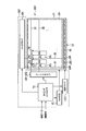
- FIG. 4 is a diagram showing main components of the display device shown in FIG.
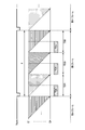
- FIG. 5 is a timing chart for explaining the display operation of the display device shown in FIG.
- FIG. 6 is a timing chart for explaining the display operation of the display device shown in FIG.
- FIG. 7 is a timing chart for explaining the first comparative example for the display operation shown in FIG.
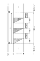
- FIG. 8 is a timing chart for explaining the second comparative example for the display operation shown in FIG.
- FIG. 9 is another timing chart for explaining the display operation of the display device shown in FIG.
- the display device of the present embodiment can be used in various devices such as smartphones, tablet terminals, and mobile phone terminals.
- FIG. 1 is a plan view showing a configuration example of the display device DSP in this embodiment.
- the first direction X and the second direction Y are directions intersecting with each other
- the third direction Z is a direction intersecting with the first direction X and the second direction Y.
- the first direction X, the second direction Y, and the third direction Z are orthogonal to each other, but may intersect with each other at an angle other than 90 degrees.
- the display device DSP includes a display panel PNL, wiring boards F1 to F5, and the like.
- the display panel PNL includes a display area DA for displaying an image and a frame-shaped non-display area NDA surrounding the display area DA.
- the display area DA includes n scanning lines G (G1 to Gn), m signal lines S (S1 to Sm), and the like. Both n and m are positive integers, and n may be equal to m or n may be different from m.
- the plurality of scanning lines G extend in the first direction X and are arranged in the second direction Y at intervals.
- Each of the plurality of signal lines S extends in the second direction Y and is arranged in the first direction X at intervals.
- the display panel PNL has ends E1 and E2 along the first direction X and ends E3 and E4 along the second direction Y.
- the width W1 of the end portion E1 and the display area DA along the second direction Y is smaller than the width W2 of the end portion E2 and the display area DA along the second direction Y.
- the width W3 of the end portion E3 and the display area DA along the first direction X is equal to the width W4 of the end portion E4 and the display area DA along the first direction X.
- the widths W3 and W4 are smaller than the width W2.
- the widths W3 and W4 may be equal to the width W1 or may be different from the width W1.
- the wiring boards F1 to F3 are arranged in this order in the first direction X.
- the wiring board F1 includes a gate driver GD1.
- the wiring board F2 includes a source driver SD.
- the wiring board F3 includes a gate driver GD2.
- the wiring boards F1 to F3 are connected to the display panel PNL and the wiring board F4, respectively.
- the wiring board F5 includes a timing controller TC, a power supply circuit PC, and the like.
- the wiring board F4 is connected to the connector CT of the wiring board F5.
- the wiring boards F1 to F3 may be replaced with a single wiring board.
- the wiring boards F1 to F4 may be replaced with a single wiring board.
- the gate driver GD and the source driver SD are not limited to those mounted on the wiring boards F1 to F3, and may be directly mounted on the display panel PNL in the non-display area NDA of the display panel PNL.
- the odd-numbered scan lines from the end E1 side are connected to the gate driver GD2 and the even-numbered scan lines are connected to the gate driver GD1, but the gate drivers GD1 and GD2 and each scan line are connected.
- the connection relationship of is not limited to the illustrated example.
- FIG. 2 is a sectional view of the display device DSP shown in FIG.
- the cross section of the display device DSP in the YZ plane defined by the second direction Y and the third direction Z only the main part will be described.
- the display panel PNL includes a first substrate SUB1, a second substrate SUB2, a liquid crystal layer LC and the like.
- the first substrate SUB1 includes a transparent substrate 10, pixel electrodes 11, an alignment film 12 and the like.
- the second substrate SUB2 includes a transparent substrate 20, a common electrode 21, an alignment film 22 and the like.
- the pixel electrode 11 and the common electrode 21 are formed of a transparent conductive material such as indium tin oxide (ITO) or indium zinc oxide (IZO).
- the liquid crystal layer LC includes polymer dispersed liquid crystal and is located between the alignment films 12 and 22.
- the first substrate SUB1 and the second substrate SUB2 are adhered by a seal SE.
- the first substrate SUB1 has an extending portion EX extending in the second direction Y beyond the end portion E5 of the transparent substrate 20.
- the wiring boards F1 to F3 are connected to the extending portion EX of the first board SUB1.
- the light source unit LU includes a light emitting element LS, a wiring board F6, and the like.
- the light emitting element LS is connected to the wiring board F6 and is located on the extending portion EX.
- the light emitting element LS has a light emitting portion EM facing the end portion E5. The illumination light emitted from the light emitting portion EM enters from the end portion E5 and propagates through the display panel PNL.
- FIG. 3 is a schematic cross-sectional view of the display panel PNL for explaining a configuration example of the liquid crystal layer LC.
- the liquid crystal layer LC has a linear (network) polymer 30 and liquid crystal molecules 31.
- polymer 30 is a liquid crystalline polymer.
- the liquid crystal molecules 31 are dispersed in the gaps between the polymers 30.
- a liquid crystal monomer is injected between the alignment film 12 and the alignment film 22, and the liquid crystal monomer aligned in a predetermined direction by the alignment regulating force of the alignment films 12 and 22 is irradiated with ultraviolet light. It is obtained by irradiating. That is, the liquid crystal monomer is polymerized by ultraviolet light, and the linear polymer 30 is formed.
- Each of the polymer 30 and the liquid crystal molecule 31 has optical anisotropy or refractive index anisotropy.
- the response of the polymer 30 to the electric field is lower than the response of the liquid crystal molecules 31 to the electric field.
- the orientation direction of the polymer 30 hardly changes regardless of the electric field between the pixel electrode 11 and the common electrode 21.
- the alignment direction of the liquid crystal molecules 31 changes according to the electric field.
- the liquid crystal molecules 31 shown by solid lines represent the alignment state when there is no potential difference between the pixel electrode 11 and the common electrode 21 (when no electric field is formed). Further, the liquid crystal molecule 31 shown by the broken line represents an alignment state when there is a potential difference between the pixel electrode 11 and the common electrode 21 (when an electric field is formed).
- the optical axes of the polymer 30 and the liquid crystal molecule 31 are substantially parallel to each other. Therefore, the light incident on the liquid crystal layer LC is transmitted with almost no scattering in the liquid crystal layer LC.
- a transparent state such a state is referred to as a transparent state.
- the voltage of the pixel electrode 11 for realizing the transparent state is referred to as a transparent voltage.
- the transparent voltage may be the same as the common voltage applied to the common electrode 21, or may be a voltage slightly different from the common voltage.
- the optical axes of the polymer 30 and the liquid crystal molecules 31 intersect each other. Therefore, the light incident on the liquid crystal layer LC is scattered in the liquid crystal layer LC.
- a scattering state such a state will be referred to as a scattering state.
- the voltage of the pixel electrode 11 for realizing the scattered state is referred to as the scattered voltage.
- the scattered voltage is a voltage such that the potential difference from the common electrode 21 is larger than the transparent voltage, and in the present embodiment, the voltages corresponding to red, green, and blue image components described later correspond to this.
- FIG. 4 is a diagram showing main components of the display device DSP shown in FIG.
- the display device DSP includes a controller CNT indicated by a dotted line in the figure.
- the controller CNT includes a timing controller TC, gate drivers GD1 and GD2, a source driver SD, a Vcom circuit VC, a light source driver LSD and the like.
- the timing controller TC generates various signals based on image data, synchronization signals, etc. input from the outside.
- the timing controller TC outputs a video component (video signal) generated by performing predetermined signal processing based on the image data (video data) to the source driver SD.
- the timing controller TC outputs the control signal generated based on the synchronization signal to the gate drivers GD1 and GD2, the source driver SD, the Vcom circuit VC, and the light source driver LSD, respectively.
- a display area DA shown by a dashed line in the figure includes a plurality of pixels PX.
- Each pixel PX includes a switching element SW and a pixel electrode 11.
- the switching element SW is electrically connected to the scanning line G and the signal line S.
- the switching element SW includes a semiconductor layer, and this semiconductor layer is formed of amorphous silicon (a-Si), an oxide semiconductor, low temperature polycrystal polysilicon (LTPS), or the like.
- the pixel electrode 11 is connected to the signal line S via the switching element SW.
- the common electrode 21 faces the plurality of pixel electrodes 11.
- a scanning signal is supplied to each of the scanning lines G from the gate driver GD1 or GD2.
- a video component is supplied to each of the signal lines S from the source driver SD.
- a common voltage is supplied to the common electrode 21 from the Vcom circuit VC.
- the video component supplied to the signal line S is supplied to the pixel electrode 11 connected to the switching element SW during the period when the switching element SW is in the conductive state based on the scanning signal supplied to the scanning line G. ..
- supplying a video component to the pixel electrode 11 to form a potential difference between the pixel electrode 11 and the common electrode 21 is referred to as a video component (or a video component in the pixel PX including the pixel electrode 11). It may be described as writing a corresponding voltage).
- setting the voltage of the pixel electrode 11 to the transparent voltage means that the video component written in the pixel PX including the pixel electrode 11 concerned. May be described as deleted.
- FIG. 4 shows the common electrode 21 over the entire display area DA.
- a plurality of common electrodes 21 divided for at least one pixel PX are arranged in the display area DA, each common electrode 21 is connected to a common line, and each common electrode from the Vcom circuit VC is connected via the common line.
- a common voltage may be supplied to 21.
- the light source unit LU includes, as the light emitting elements LS, a light emitting element LSR that emits red light, a light emitting element LSG that emits green light, and a light emitting element LSB that emits blue light.
- a light emitting diode LED
- the light source driver LSD controls the lighting period of these light emitting elements LSR, LSG, LSB based on the control signal from the timing controller TC.
- the image components corresponding to red, green, and blue are written in a time-divisional manner, and the light-emitting elements of the colors corresponding to the written image components are lighted in a time-divisional manner in one frame period described later. It is assumed that the display device DSP is driven by the field sequential method.
- FIG. 5 is a timing chart showing an example of the display operation in the display device DSP according to this embodiment.
- the vertical synchronization signal Vsync falls. That is, in the example of FIG. 5, the period from the fall of the vertical synchronization signal Vsync to the fall thereof corresponds to one frame period F.
- one frame period F is about 16.7 ms.
- one frame period F includes a plurality of scanning periods TS (first period) for writing a video component in the pixel PX and a plurality of holding periods for holding the video component written in the scanning period TS.
- TH second period
- a video component of the same color as the last scanning period TS of the plurality of scanning periods TS included in the immediately preceding frame period is written in the pixel PX.
- the video component written in the last scanning period TS included in the immediately preceding frame period and the video component written in the target scanning period TSS in a time division manner.
- a second scan period TS2 for writing an image component of a color different from the target scan period TSS and the first scan period TS1 into the pixel PX. ..
- the target scanning period TSS, the first scanning period TS1 and the second scanning period TS2 included in the one frame period F are respectively a red scanning period TSR for writing a red image component in the pixel PX and a green image component in the pixel PX.
- a red scanning period TSR for writing a red image component in the pixel PX
- a green image component in the pixel PX Corresponding to either the green scanning period TSG for writing in the pixel or the blue scanning period TSB for writing the blue image component in the pixel PX.
- the target holding period THS and the first holding period TH1 included in the one frame period F are respectively the red holding period THR and the green scanning period TSG for holding the red image component written in the red scanning period TSR. It corresponds to one of the green holding period THG for holding the written green image component and the blue holding period THB for holding the written blue image component in the blue scanning period TSB.
- Each scanning period TS and each holding period TH included in one frame period F may be referred to as a subframe. Further, each holding period TH may be referred to as a blanking period.
- one frame period F includes the target scanning period TSS, the target holding period THS, the first scanning period TS1, the first holding period TH1 and the second scanning period TS2 as described above.
- the one frame period F may further include a blanking period immediately before the target scanning period TSS, or may further include a blanking period immediately after the second scanning period TS2.
- the one frame period F may further include, for example, a period in which the transparent voltage is applied immediately after each holding period TH to erase the held image component.
- the one frame period F will be specifically described by focusing on the Xth frame in FIG.
- the red scanning period TSR2 for writing the same red image component as the last scanning period TSR1 included in the X-1th frame which is the immediately preceding frame period into the pixel PX is set. It is provided.
- the red scanning period TSR2 includes n horizontal scanning periods as many as the scanning lines G1 to Gn.
- the horizontal scanning period may be referred to as a horizontal period.
- the gate drivers GD1 and GD2 sequentially supply scanning signals to the scanning lines G1 to Gn.
- the source driver SD supplies a voltage (scattering voltage) corresponding to the red image component to each of the signal lines S1 to Sm. More specifically, the operation of simultaneously supplying the gradation voltages corresponding to the pixels PX of the line to which the scanning signal is supplied to the signal lines S1 to Sm is repeated.
- a voltage according to the red image component is written between the pixel electrode 11 and the common electrode 21 of each pixel PX.
- the time required until the voltage according to the red image component is written in all the pixels PX, that is, the red scanning period TSR2 is 3.33 ms, for example.
- the liquid crystal (the liquid crystal molecule 31) responds to the red image component written in the last scanning period TSR1 included in the X-1th frame which is the immediately preceding frame period as the target holding period THS.
- the red holding period THR is provided with the timing of starting the operation as a starting point.
- the target holding period THS overlaps the target scanning period TSS.
- the red light emitting element LSR is turned on. According to this, the red image component written in the last scanning period TSR1 included in the X-1th frame and the red image component written in the red scanning period TSR2 that is the target scanning period TSS are obtained. A red image (image) is displayed in the display area DA.
- the first scanning period TS1 for writing a video component of a color different from the red scanning period TSR2 which is the target scanning period TSS is set.
- Green scanning period TSG is provided.
- the green scanning period TSG is provided as the first scanning period TS1 is illustrated, but the present invention is not limited to this, and the first scanning period TS1 includes the target scanning period TSS (in this case, The blue scanning period TSB may be provided as the first scanning period TS1 as long as it is a period for writing a video component of a color different from the red scanning period TSR2).
- the green scanning period TSG is provided as the second scanning period TS2 described later.
- the green scanning period TSG includes n horizontal scanning periods as many as the scanning lines G1 to Gn, and in each horizontal scanning period, the gate drivers GD1 and GD2 each scan line G1 to Gn.
- the scanning signals are sequentially supplied to. Further, during the supply of this scanning signal, the source driver SD supplies a voltage corresponding to the green image component to each of the signal lines S1 to Sm.
- the green scanning period TSG is 3.33 ms, for example, like the red scanning period TSR2.
- the light emitting element LS is turned off during the first scanning period TS1.
- a green holding period THG is provided.
- the green light emitting element LSG is turned on. According to this, the green image corresponding to the green image component written in the green scanning period TSG which is the first scanning period TS1 is displayed in the display area DA.
- the time during which the green image is displayed in the display area DA, that is, the green holding period THG is 3.33 ms, for example.
- the second scanning period TS2 for writing the image component of a color different from the target scanning period TSS and the first scanning period TS1. Also, a blue scanning period TSB is provided as the last scanning period TS included in the Xth frame.
- the blue scanning period TSB includes n horizontal scanning periods as many as the scanning lines G1 to Gn, and in each horizontal scanning period, the gate drivers GD1 and GD2 respectively Scan signals are sequentially supplied to the scan lines G1 to Gn. Further, during the supply of this scanning signal, the source driver SD supplies a voltage corresponding to the blue image component to each of the signal lines S1 to Sm.
- the blue scanning period TSB is, for example, 3.33 ms, like the red scanning period TSR2 and the green scanning period TSG.
- the light emitting element LS is turned off during the second scanning period TS2.
- the blue scanning period TSB for writing the video component of the same color as the blue scanning period TSB which is the last scanning period TS of the Xth frame is It is provided as the target scanning period TSS in the X+1 frame. Further, in the (X+1)th frame, a blue holding period THB that overlaps the blue scanning period TSB that is the target scanning period TSS is provided as the target holding period THS.
- FIG. 6 shows a timing chart when the display operation in the display device DSP shown in FIG. 5 is executed over a plurality of frames.
- the green scanning period TSG2 for writing the same green image component as the last scanning period TSG1 included in the X-1th frame which is the immediately preceding frame period into the pixel PX. Is provided.
- the target holding period THS As the target holding period THS, the timing at which the liquid crystal starts to respond to the green image component written in the last scanning period TSG1 included in the X-1th frame which is the immediately preceding frame period is the starting point.
- the green holding period THG is set. As shown in FIG. 5, the target holding period THS overlaps the target scanning period TSS (in this case, the green holding period THG).
- a first scanning period TS1 for writing a video component of a color different from the green scanning period TSG2 which is the target scanning period TSS is set.
- a blue scanning period TSB is provided.
- a blue holding period THB is provided.
- the second scanning period TS2 for writing the image component of a color different from the target scanning period TSS and the first scanning period TS1.
- a red scanning period TSR1 is provided.
- the red scanning period TSR1 corresponds to the last scanning period TS in the Xth frame.
- a red scanning period TSR2 for writing the same red image component as the last scanning period TSR1 included in the Xth frame, which is the immediately preceding frame period, into the pixel PX is set as the target scanning period TSS. It is provided.
- the target holding period THS As the target holding period THS, the timing at which the liquid crystal starts to respond to the red image component written in the last scanning period TSR1 included in the Xth frame which is the immediately preceding frame period is set as the starting point.
- a red holding period THR is provided.
- the target holding period THS (red holding period THR in this case) in the (X+1)th frame is overlapped with the target scanning period TSS (red scanning period TSR2 in this case), as in the Xth frame.
- a green scanning period TSG is provided as a first scanning period TS1 for writing a video component of the same color as the target scanning period TSS).
- a green holding period THG is provided.
- the second scanning period TS2 for writing the image component of a color different from the target scanning period TSS and the first scanning period TS1.
- the blue scanning period TSB1 is provided.
- the blue scanning period TSB1 corresponds to the last scanning period TS in the (X+1)th frame.
- a blue scanning period TSB2 for writing the same blue video component as the last scanning period TSB1 included in the X+1th frame which is the immediately preceding frame period into the pixel PX is set as the target scanning period TSS. It is provided.
- the start point is the timing at which the liquid crystal starts to respond to the blue image component written in the last scanning period TSB1 included in the X+1th frame, which is the immediately preceding frame period, as the target holding period THS.
- a blue holding period THB is provided.
- the target holding period THS (blue holding period THB in this case) in the (X+2)th frame is overlapped with the target scanning period TSS (blue scanning period TSB2 in this case) similarly to the Xth frame and the X+1th frame.
- a red scanning period TSR is provided as a first scanning period TS1 for writing a video component of the same color as the target scanning period TSS).
- a red holding period THR is provided.
- the green scanning period TSG1 is provided.
- This green scanning period TSG1 corresponds to the last scanning period TS in the (X+2)th frame.
- the configuration of the (X-1)th frame is the same as the configuration of the (X+2)th frame.
- the first comparative example and the second comparative example are for explaining some of the effects that the display device DSP according to the present embodiment can achieve, and the configurations common to these comparative example and the present embodiment.
- the effects and advantages are not excluded from the scope of the present invention.
- FIG. 7 is a timing chart showing an example of the display operation according to the first comparative example.
- the 1-frame period F according to the first comparative example includes a blue display period TDB for displaying an image corresponding to the blue image component written in the immediately preceding frame period and a red frame period as shown in the Xth frame.
- the blue light emitting element LSB is turned on in the blue display period TDB
- the red light emitting element LSR is turned on in the red display period TDR
- the green light emitting element LSG is turned on in the green display period TDG.
- the blue display period TDB and the red scanning period TSR overlap each other.
- the red display period TDR and the green scanning period TSG overlap each other.
- the green display period TDG and the blue scanning period TSB overlap each other.
- each scanning period TSR, TSG, TSB is, for example, 5.55 ms.
- the display periods TDR, TDG, TDB are, for example, 2.78 ms, respectively.
- FIG. 8 is a timing chart showing an example of the display operation according to the second comparative example.
- a scanning period TS for writing the image component corresponding to each color in the pixel PX and a holding period for holding the image component corresponding to each color written in the pixel PX It is provided so as not to overlap with TH.
- one frame period F according to the second comparative example includes a red scanning period TSR, a red holding period THR, a green scanning period TSG, a green holding period THG, and a blue scanning period TSB as shown in the Xth frame.
- a blue holding period THB, and a scanning period TS and a holding period TH corresponding to each color are arranged in order.
- FIG. 8 illustrates the case where the scanning period TS and the holding period TH are sequentially arranged in the order of red, green, and blue
- the present invention is not limited to this, and the order of each color may be an arbitrary order. Absent.
- the scanning period TS and the holding period TH may be arranged in order of green, blue, and red, or the scanning period TS and the holding period TH may be arranged in order of blue, red, and green.
- each scanning period TSR, TSG, TSB and each holding period THR, THG, THB are, for example, 2.78 ms, respectively.
- the light emitting element LS corresponding to each color is turned on only in the holding period TH corresponding to each color, and is turned off in the scanning period TS corresponding to each color. Therefore, while the light emitting element LS corresponding to the color of the video component written in the scan period TS immediately before is turned on, the video component of another color is not written in the pixel PX. It is possible to suppress the occurrence of color breakup.
- the maximum assignable time for each scanning period TSR, TSG, TSB is 2.78 ms obtained by dividing one frame period F into six as described above. According to this, for example, when the number of the scanning lines G provided in the display device DSP increases and the driving load increases, a sufficient time for writing the image component corresponding to each color into the pixel PX is obtained. There is an inconvenience that you cannot do it. That is, there is an inconvenience that the display area DA provided in the display device DSP cannot be increased in size or high definition.
- the one frame period F is configured to include the target scanning period TSS and the target holding period THS, so that the period corresponding to the blue holding period THB shown in FIG. Can be omitted. According to this, it is possible to divide one frame period F into five divisions instead of six divisions. Therefore, when the display device DSP is driven at 60 Hz, the time that can be assigned to each scanning period TSR, TSG, and TSB is set to two. It can be from 0.78 ms to 3.33 ms.
- each scanning period TSR, TSG, TSB but also each holding period THR, THG, THB can be made longer. Since it is possible, it is possible to further increase the brightness of the pixel PX in which the video component corresponding to each color is written. That is, it is possible to provide a brighter image to the user as compared with the case where the display operation according to the second comparative example is performed.
- the holding periods THR, THG, and THB can be made longer than those in the display operation according to the second comparative example, and thus the light emitting element LS is possible. Even if the amount of light is reduced, it is possible to realize the same brightness as in the case of the display operation according to the second comparative example. According to this, it is possible to realize power saving by the amount of reduction of the light amount of the light emitting element LS.
- FIG. 9A shows the display operation according to the second comparative example
- FIG. 9B shows the display operation according to the present embodiment.
- the time of the scanning period TS included in one frame period F is not the 3.33 ms shown in FIG. 5 (and FIG. 6) but the second comparison time. This is different from the case shown in FIG. 5 (and FIG. 6) in that the display operation is set to 2.78 ms like the display operation according to the example.
- the display operation according to the present embodiment when the size of the display area DA provided in the display device DSP is sufficient for the display operation according to the second comparative example, that is, the time for writing the video component corresponding to each color in the pixel PX is 2
- the period corresponding to the blue holding period THB shown in FIG. 9A can be omitted. Therefore, it is possible to shorten the one frame period F as compared with the display operation according to the second comparative example. That is, according to the display operation according to the present embodiment, it is possible to improve the frame rate by about 1.2 times as compared with the case according to the second comparative example, and thus improve the image display performance. It is possible to expect.
- Vsync Vertical sync signal, G1 to Gn... Scan line, F... 1 frame period, TS... Scan period, TSS... Target scan period, TS1... First scan period, TS2... Second scan period, TSR... Red scan period, TSG... Green scanning period, TSB... Blue scanning period, TH... Holding period, THS... Target holding period, TH1... First holding period, THR... Red holding period, THG... Green holding period, THB... Blue holding period.
Landscapes
- Engineering & Computer Science (AREA)
- Physics & Mathematics (AREA)
- Computer Hardware Design (AREA)
- General Physics & Mathematics (AREA)
- Theoretical Computer Science (AREA)
- Chemical & Material Sciences (AREA)
- Crystallography & Structural Chemistry (AREA)
- Power Engineering (AREA)
- Control Of Indicators Other Than Cathode Ray Tubes (AREA)
- Liquid Crystal (AREA)
- Liquid Crystal Display Device Control (AREA)
Abstract
表示品位を向上させることが可能な表示装置および表示方法を提供すること。 一実施形態における表示装置は、表示パネルと、光源と、コントローラとを備える。コントローラは、1フレーム期間に含まれる複数の第1期間において共通電極と画素電極との間の電圧を制御し、かつ、1フレーム期間に含まれる複数の第2期間において光源の動作を制御する。コントローラは、1フレーム期間に含まれる複数の第1期間のうちの最初の第1期間においては、直前の1フレーム期間に含まれる複数の第1期間のうちの最後の第1期間において、共通電極と画素電極との間に電圧を印加して書き込んだ映像成分と同じ色の映像成分を、直前の1フレーム期間に続けて書き込むよう、共通電極と画素電極との間の電圧を制御する。
Description
本発明の実施形態は、表示装置および表示方法に関する。
近年、光源と、画素電極および共通電極を含む一対の基板と、これら基板の間に配置された高分子分散型の液晶層とを備えた表示装置が知られている。例えば、高分子分散型の液晶層は、筋状のポリマーと、液晶分子とを含む。
高分子分散型の液晶層においては、画素電極および共通電極の間の電界により液晶分子を回転させることで、ポリマーの光軸に対する液晶分子の光軸の傾きを制御することができる。これにより、画素毎に光源からの光の散乱度を制御し、表示装置に任意の映像(画像)を表示させることが可能となる。
高分子分散型の液晶層を備える表示装置において、さらなる表示品位の改善が求められている。そこで、本開示は、表示品位を向上させることが可能な表示装置および表示方法を提供することを目的の一つとする。
一実施形態における表示装置は、表示パネルと、光源と、コントローラとを具備する。前記表示パネルは、マトリクス状に配置された複数の画素と、共通電極と、前記画素毎に設けられた画素電極と、液晶層と、を含む。前記光源は、前記表示パネルに光を照射する。前記コントローラは、1フレーム期間に含まれる複数の第1期間において前記共通電極と前記画素電極との間の電圧を制御し、かつ、前記1フレーム期間に含まれる複数の第2期間において前記光源の動作を制御する。前記コントローラは、前記1フレーム期間に含まれる複数の第1期間のうちの最初の第1期間においては、直前の1フレーム期間に含まれる複数の第1期間のうちの最後の第1期間において、前記共通電極と前記画素電極との間に電圧を印加して書き込んだ映像成分と同じ色の映像成分を、前記直前の1フレーム期間に続けて書き込むよう、前記共通電極と前記画素電極との間の電圧を制御する。
本実施形態によれば、表示品位を向上させることが可能な表示装置および表示方法を提供することができる。
以下、実施の形態について図面を参照して説明する。
なお、開示はあくまで一例に過ぎず、当業者において、発明の主旨を保っての適宜変更について容易に想到し得るものについては、当然に本発明の範囲に含有される。また、図面は、説明をより明確にするため、実際の態様に比べて模式的に表される場合があるが、あくまで一例であって、本発明の解釈を限定するものではない。また、本明細書と各図において、既出の図に関して前述したものと同一または類似した機能を発揮する構成要素には同一の参照符号を付し、重複する説明を省略することがある。
なお、開示はあくまで一例に過ぎず、当業者において、発明の主旨を保っての適宜変更について容易に想到し得るものについては、当然に本発明の範囲に含有される。また、図面は、説明をより明確にするため、実際の態様に比べて模式的に表される場合があるが、あくまで一例であって、本発明の解釈を限定するものではない。また、本明細書と各図において、既出の図に関して前述したものと同一または類似した機能を発揮する構成要素には同一の参照符号を付し、重複する説明を省略することがある。
以下では、表示装置の一例として、高分子分散型液晶を適用した表示装置について説明する。本実施形態の表示装置は、例えば、スマートフォン、タブレット端末、携帯電話端末等の種々の装置に用いることができる。
図1は、本実施形態における表示装置DSPの構成例を示す平面図である。図中において、第1方向Xおよび第2方向Yは互いに交差する方向であり、第3方向Zは第1方向Xおよび第2方向Yと交差する方向である。一例では、第1方向X、第2方向Yおよび第3方向Zは、互いに直交しているが、互いに90度以外の角度で交差していても良い。
表示装置DSPは、表示パネルPNL、配線基板F1乃至F5等を備えている。表示パネルPNLは、画像を表示する表示領域DA、および、表示領域DAを囲む額縁状の非表示領域NDAを備えている。表示領域DAは、n本の走査線G(G1乃至Gn)、m本の信号線S(S1乃至Sm)等を備えている。なお、nおよびmはいずれも正の整数であり、nがmと等しくても良いし、nがmとは異なっていても良い。複数の走査線Gは、それぞれ第1方向Xに延出し、第2方向Yに間隔をおいて並んでいる。複数の信号線Sは、それぞれ第2方向Yに延出し、第1方向Xに間隔をおいて並んでいる。
表示パネルPNLは、第1方向Xに沿った端部E1およびE2と、第2方向Yに沿った端部E3およびE4とを有している。非表示領域NDAの幅について、端部E1と表示領域DAとの第2方向Yに沿った幅W1は、端部E2と表示領域DAとの第2方向Yに沿った幅W2より小さい。また、端部E3と表示領域DAとの第1方向Xに沿った幅W3は、端部E4と表示領域DAとの第1方向Xに沿った幅W4と同等である。また、幅W3およびW4は、幅W2より小さい。また、幅W3およびW4は、幅W1と同等であっても良いし、幅W1とは異なっていても良い。
配線基板F1乃至F3は、この順に第1方向Xに並んでいる。配線基板F1は、ゲートドライバGD1を備えている。配線基板F2は、ソースドライバSDを備えている。配線基板F3は、ゲートドライバGD2を備えている。配線基板F1乃至F3は、それぞれ表示パネルPNLおよび配線基板F4に接続されている。配線基板F5は、タイミングコントローラTCや電源回路PC等を備えている。配線基板F4は、配線基板F5のコネクタCTに接続されている。なお、配線基板F1乃至F3は、単一の配線基板に置換されても良い。また、配線基板F1乃至F4は、単一の配線基板に置換されても良い。さらに、ゲートドライバGDやソースドライバSDは配線基板F1乃至F3に実装されるものに限らず、表示パネルPNLの非表示領域NDAにて直接表示パネルPNLに実装されるものであっても良い。
図示した例では、端部E1の側から奇数番目の走査線がゲートドライバGD2に接続され、偶数番目の走査線がゲートドライバGD1に接続されているが、ゲートドライバGD1およびGD2と各走査線との接続関係は図示した例に限らない。
図2は、図1に示した表示装置DSPの断面図である。ここでは、第2方向Yおよび第3方向Zによって規定されるY-Z平面における表示装置DSPの断面において、主要部のみを説明する。
表示パネルPNLは、第1基板SUB1、第2基板SUB2、液晶層LC等を備えている。第1基板SUB1は、透明基板10、画素電極11、配向膜12等を備えている。第2基板SUB2は、透明基板20、共通電極21、配向膜22等を備えている。画素電極11および共通電極21は、例えばインジウム錫酸化物(ITO)やインジウム亜鉛酸化物(IZO)等の透明導電材料によって形成されている。液晶層LCは、高分子分散液晶を含み、配向膜12と配向膜22との間に位置している。第1基板SUB1および第2基板SUB2は、シールSEによって接着されている。第1基板SUB1は、透明基板20の端部E5よりも第2方向Yに延出した延出部EXを有している。
配線基板F1乃至F3は、第1基板SUB1の延出部EXに接続されている。
配線基板F1乃至F3は、第1基板SUB1の延出部EXに接続されている。
光源ユニットLUは、発光素子LS、配線基板F6等を備えている。発光素子LSは、配線基板F6に接続され、延出部EXの上に位置している。発光素子LSは、端部E5と対向する発光部EMを有している。発光部EMから出射された照明光は、端部E5から入射し、表示パネルPNLを伝播する。
図3は、液晶層LCの構成例を説明するための、表示パネルPNLの概略的な断面図である。本実施形態において、液晶層LCは、筋状(ネットワーク状)のポリマー30と、液晶分子31とを有している。一例では、ポリマー30は、液晶性ポリマーである。液晶分子31は、ポリマー30の隙間に分散されている。図3に示すように、ポリマー30に接続されたモノマー32が存在しても良い。
このような液晶層LCは、例えば配向膜12と配向膜22との間に液晶モノマーを注入し、これら配向膜12および22の配向規制力により所定方向に配向された液晶モノマーに対して紫外光を照射することで得られる。すなわち、紫外光により液晶モノマーが高分子化され、筋状のポリマー30が形成される。
ポリマー30および液晶分子31の各々は、光学異方性あるいは屈折率異方性を有している。ポリマー30の電界に対する応答性は、液晶分子31の電界に対する応答性より低い。例えば、ポリマー30の配向方向は、画素電極11と共通電極21との間の電界に関わらずほとんど変化しない。一方、液晶分子31の配向方向は、当該電界に応じて変化する。
図3において、実線で示す液晶分子31は、画素電極11と共通電極21との間に電位差が無い場合(電界が形成されていない場合)の配向状態を表している。また、破線で示す液晶分子31は、画素電極11と共通電極21との間に電位差がある場合(電界が形成されている場合)の配向状態を表している。
液晶層LCに電界が作用していないか、あるいは当該電界が極めて弱い状態においては、ポリマー30および液晶分子31のそれぞれの光軸は互いに略平行となる。したがって、液晶層LCに入射した光は、液晶層LC内でほとんど散乱されることなく透過する。以下では、このような状態を透明状態と称する。また、透明状態を実現するための画素電極11の電圧を透明電圧と称する。透明電圧は、共通電極21に印加される共通電圧と同じであっても良いし、共通電圧と僅かに異なる電圧であっても良い。
一方、液晶層LCに十分な電界が作用している状態では、ポリマー30および液晶分子31のそれぞれの光軸は互いに交差する。したがって、液晶層LCに入射した光は、液晶層LC内で散乱される。以下では、このような状態を散乱状態と称する。また、散乱状態を実現するための画素電極11の電圧を散乱電圧と称する。散乱電圧は、透明電圧よりも共通電極21との電位差が大きくなるような電圧であり、本実施形態においては、後述する赤色、緑色、青色の映像成分に応じた電圧がこれに相当する。
なお、液晶分子31が、図3の実線の状態から破線の状態に遷移するまでには、画素電極11に散乱電圧が印加されてから僅かな時間を要する。つまり、散乱電圧が画素電極11に印加されたタイミングと、液晶分子31が実線の状態から破線の状態に遷移するタイミング(要するに、液晶分子31が散乱電圧に応答するタイミング)とは僅かに異なっている。
図4は、図1に示した表示装置DSPの主要な構成要素を示す図である。
表示装置DSPは、図中に点線で示すコントローラCNTを備えている。コントローラCNTは、タイミングコントローラTC、ゲートドライバGD1およびGD2、ソースドライバSD、Vcom回路VC、光源ドライバLSD等を含む。
表示装置DSPは、図中に点線で示すコントローラCNTを備えている。コントローラCNTは、タイミングコントローラTC、ゲートドライバGD1およびGD2、ソースドライバSD、Vcom回路VC、光源ドライバLSD等を含む。
タイミングコントローラTCは、外部から入力された画像データや同期信号等に基づいて各種信号を生成する。一例では、タイミングコントローラTCは、画像データ(映像データ)に基づき、所定の信号処理を行って生成した映像成分(映像信号)をソースドライバSDに出力する。また、タイミングコントローラTCは、同期信号に基づいて生成した制御信号を、ゲートドライバGD1およびGD2、ソースドライバSD、Vcom回路VC、光源ドライバLSDにそれぞれ出力する。
図中に一点鎖線で示す表示領域DAは、複数の画素PXを備えている。各画素PXは、スイッチング素子SWおよび画素電極11を備えている。スイッチング素子SWは、走査線Gおよび信号線Sと電気的に接続されている。スイッチング素子SWは半導体層を備えており、この半導体層は、アモルファスシリコン(a-Si)や酸化物半導体、低温多結晶ポリシリコン(LTPS)等によって形成される。画素電極11は、スイッチング素子SWを介して信号線Sに接続されている。
共通電極21は、複数の画素電極11と対向している。走査線Gの各々には、ゲートドライバGD1またはGD2から走査信号が供給される。信号線Sの各々には、ソースドライバSDから映像成分が供給される。共通電極21には、Vcom回路VCから共通電圧が供給される。信号線Sに供給された映像成分は、走査線Gに供給された走査信号に基づいてスイッチング素子SWが導通状態となった期間に、当該スイッチング素子SWに接続された画素電極11に供給される。
以下の説明においては、画素電極11に映像成分を供給して画素電極11と共通電極21との間に電位差を形成することを、当該画素電極11を備える画素PXに映像成分(或いは映像成分に応じた電圧)を書き込むと記載することがある。また、以下の説明においては、上記した散乱状態から上記した透明状態に遷移させるために、画素電極11の電圧を透明電圧とすることを、当該画素電極11を備える画素PXに書き込まれた映像成分を消去すると記載することがある。
なお、図4の例では、表示領域DAの全体にわたる共通電極21を示している。しかしながら、少なくとも1つの画素PX毎に区切られた複数の共通電極21が表示領域DAに配置され、各共通電極21が共通線にそれぞれ接続され、当該共通線を介してVcom回路VCから各共通電極21に共通電圧が供給されても良い。
光源ユニットLUは、発光素子LSとして、赤色の光を放つ発光素子LSR、緑色の光を放つ発光素子LSG、および、青色の光を放つ発光素子LSBを備えている。これら発光素子LSR、LSG、LSBとしては、例えば発光ダイオード(LED)を用いることができるが、この例に限定されない。光源ドライバLSDは、タイミングコントローラTCからの制御信号に基づいて、これら発光素子LSR、LSG、LSBの点灯期間を制御する。なお、本実施形態においては、後述する1フレーム期間において、赤色、緑色、青色に対応した映像成分を時分割的に書き込み、書き込んだ映像成分に対応する色の発光素子を時分割的に点灯するフィールドシーケンシャル方式にて、表示装置DSPは駆動されるものとする。
図5は、本実施形態に係る表示装置DSPにおける表示動作の一例を示すタイミングチャートである。
1フレーム期間Fの開始時には、垂直同期信号Vsyncが立ち下がる。すなわち、図5の例では、垂直同期信号Vsyncが立ち下がってから、再度立ち下がるまでの期間が1フレーム期間Fに相当する。例えば60Hzで表示装置DSPを駆動する場合、1フレーム期間Fは約16.7msである。
1フレーム期間Fの開始時には、垂直同期信号Vsyncが立ち下がる。すなわち、図5の例では、垂直同期信号Vsyncが立ち下がってから、再度立ち下がるまでの期間が1フレーム期間Fに相当する。例えば60Hzで表示装置DSPを駆動する場合、1フレーム期間Fは約16.7msである。
本実施形態において、1フレーム期間Fは、画素PXに映像成分を書き込むための複数の走査期間TS(第1期間)と、走査期間TSにおいて書き込まれた映像成分を保持するための複数の保持期間TH(第2期間)とを含む。
より詳しくは、本実施形態における1フレーム期間Fは、(1)直前のフレーム期間に含まれる複数の走査期間TSのうちの、最後の走査期間TSと同じ色の映像成分を画素PXに書き込むための対象走査期間TSSと、(2)直前のフレーム期間に含まれる最後の走査期間TSにおいて書き込まれた映像成分と、当該対象走査期間TSSにおいて書き込まれた映像成分とを時分割で保持するための対象保持期間THSと、(3)当該対象走査期間TSSとは異なる色の映像成分を画素PXに書き込むための第1走査期間TS1と、(4)当該第1走査期間TS1において書き込まれた映像成分を保持するための第1保持期間TH1と、(5)当該対象走査期間TSSおよび当該第1走査期間TS1とは異なる色の映像成分を画素PXに書き込むための第2走査期間TS2と、を含む。
1フレーム期間Fに含まれる対象走査期間TSS、第1走査期間TS1および第2走査期間TS2は、それぞれ、赤色の映像成分を画素PXに書き込むための赤色走査期間TSR、緑色の映像成分を画素PXに書き込むための緑色走査期間TSG、および、青色の映像成分を画素PXに書き込むための青色走査期間TSBのいずれかに該当する。
また、1フレーム期間Fに含まれる対象保持期間THSおよび第1保持期間TH1は、それぞれ、赤色走査期間TSRにおいて書き込まれた赤色の映像成分を保持するための赤色保持期間THR、緑色走査期間TSGにおいて書き込まれた緑色の映像成分を保持するための緑色保持期間THG、および、青色走査期間TSBにおいて書き込まれた青色の映像成分を保持するための青色保持期間THBのいずれかに該当する。
なお、1フレーム期間Fに含まれる各走査期間TSおよび各保持期間THはサブフレームと称されても良い。また、各保持期間THはブランキング期間と称されても良い。
なお、1フレーム期間Fに含まれる各走査期間TSおよび各保持期間THはサブフレームと称されても良い。また、各保持期間THはブランキング期間と称されても良い。
図5では、1フレーム期間Fが、上記したように、対象走査期間TSS、対象保持期間THS、第1走査期間TS1、第1保持期間TH1および第2走査期間TS2を含むとしたが、これに限定されず、1フレーム期間Fは、例えば、対象走査期間TSSの直前にブランキング期間をさらに含むとしても良いし、第2走査期間TS2の直後にブランキング期間をさらに含むとしても良い。また、1フレーム期間Fは、例えば、各保持期間THの直後に透明電圧を印加して、保持されていた映像成分を消去する期間をさらに含むとしても良い。
以下、図5の第Xフレームに着目して、1フレーム期間Fについて具体的に説明する。
第Xフレームにおいては、まず対象走査期間TSSとして、直前のフレーム期間である第X-1フレームに含まれる最後の走査期間TSR1と同じ赤色の映像成分を画素PXに書き込むための赤色走査期間TSR2が設けられている。
赤色走査期間TSR2は、走査線G1乃至Gnと同数のn個の水平走査期間を含む。なお、水平走査期間は水平期間と称されても良い。各水平走査期間においては、ゲートドライバGD1およびGD2が各走査線G1乃至Gnに走査信号を順次供給する。また、この走査信号の供給の間、ソースドライバSDが赤色の映像成分に応じた電圧(散乱電圧)を各信号線S1乃至Smに供給する。より詳しくは、走査信号が供給されたラインの各画素PXに対応する階調の電圧を一斉に各信号線S1乃至Smに供給する動作が繰り返される。
このような動作により、各画素PXの画素電極11と共通電極21との間に、赤色の映像成分に応じた電圧が書き込まれる。全ての画素PXに赤色の映像成分に応じた電圧が書き込まれるまでにかかる時間、すなわち、赤色走査期間TSR2は、例えば3.33msである。
また、第Xフレームにおいては、対象保持期間THSとして、直前のフレーム期間である第X-1フレームに含まれる最後の走査期間TSR1において書き込まれた赤色の映像成分に液晶(液晶分子31)が応答し始めるタイミングを始点とした赤色保持期間THRが設けられている。対象保持期間THSは、対象走査期間TSSと重畳している。
なお、図5においては、説明の便宜上、対象走査期間TSSと対象保持期間THSとが同じタイミングで開始される場合を例示しているが、対象保持期間THSが開始されるタイミングは、上記したように、走査期間TSR1において書き込まれた赤色の映像成分に液晶が応答し始めるタイミングであり、図5のタイミングに限定されない。
赤色保持期間THRにおいては、赤色の発光素子LSRが点灯される。これによれば、第X-1フレームに含まれる最後の走査期間TSR1において書き込まれた赤色の映像成分と、対象走査期間TSSである赤色走査期間TSR2において書き込まれた赤色の映像成分とに応じた赤色の映像(画像)が表示領域DAに表示される。なお、赤色の映像が表示領域DAに表示される時間、すなわち、赤色保持期間THRは、例えば6.66(=3.33×2)msである。
第Xフレームにおいては、対象保持期間THS(この場合、赤色保持期間THR)に続いて、対象走査期間TSSである赤色走査期間TSR2とは異なる色の映像成分を書き込むための第1走査期間TS1として、緑色走査期間TSGが設けられている。
なお、図5においては、第1走査期間TS1として、緑色走査期間TSGが設けられている場合を例示したが、これに限定されず、第1走査期間TS1は、対象走査期間TSS(この場合、赤色走査期間TSR2)と異なる色の映像成分を書き込むための期間であれば良いので、青色走査期間TSBが第1走査期間TS1として設けられても良い。この場合、緑色走査期間TSGが、後述する第2走査期間TS2として設けられる。
緑色走査期間TSGは、赤色走査期間TSR2と同様に、走査線G1乃至Gnと同数のn個の水平走査期間を含み、各水平走査期間においては、ゲートドライバGD1およびGD2が各走査線G1乃至Gnに走査信号を順次供給する。また、この走査信号の供給の間、ソースドライバSDが緑色の映像成分に応じた電圧を各信号線S1乃至Smに供給する。
このような動作により、各画素PXの画素電極11と共通電極21との間に、緑色の映像成分に応じた電圧が書き込まれる。全ての画素PXに緑色の映像成分に応じた電圧が書き込まれるまでにかかる時間、すなわち、緑色走査期間TSGは、赤色走査期間TSR2と同様に、例えば3.33msである。
なお、第1走査期間TS1の間、発光素子LSは消灯される。
第Xフレームにおいては、第1走査期間TS1(この場合、緑色走査期間TSG)に続いて、当該第1走査期間TS1において書き込まれた緑色の映像成分を保持するための第1保持期間TH1として、緑色保持期間THGが設けられている。
緑色保持期間THGにおいては、緑色の発光素子LSGが点灯される。これによれば、第1走査期間TS1である緑色走査期間TSGにおいて書き込まれた緑色の映像成分に応じた緑色の映像が表示領域DAに表示される。なお、緑色の映像が表示領域DAに表示される時間、すなわち、緑色保持期間THGは、例えば3.33msである。
第Xフレームにおいては、第1保持期間TH1(この場合、緑色保持期間THG)に続いて、対象走査期間TSSおよび第1走査期間TS1とは異なる色の映像成分を書き込むための第2走査期間TS2として、また、当該第Xフレームに含まれる最後の走査期間TSとして、青色走査期間TSBが設けられている。
青色走査期間TSBは、赤色走査期間TSR2および緑色走査期間TSGと同様に、走査線G1乃至Gnと同数のn個の水平走査期間を含み、各水平走査期間においては、ゲートドライバGD1およびGD2が各走査線G1乃至Gnに走査信号を順次供給する。また、この走査信号の供給の間、ソースドライバSDが青色の映像成分に応じた電圧を各信号線S1乃至Smに供給する。
このような動作により、各画素PXの画素電極11と共通電極21との間に、青色の映像成分に応じた電圧が書き込まれる。全ての画素PXに青色の映像成分に応じた電圧が書き込まれるまでにかかる時間、すなわち、青色走査期間TSBは、赤色走査期間TSR2および緑色走査期間TSGと同様に、例えば3.33msである。
なお、第2走査期間TS2の間、発光素子LSは消灯される。
第Xフレームの次のフレーム期間である第X+1フレームの開始時には、当該第Xフレームの最後の走査期間TSである青色走査期間TSBと同じ色の映像成分を書き込むための青色走査期間TSBが、第X+1フレームにおける対象走査期間TSSとして設けられる。また、第X+1フレームにおいては、対象走査期間TSSである青色走査期間TSBと重畳する青色保持期間THBが対象保持期間THSとして設けられる。
図6は、図5に示す表示装置DSPにおける表示動作が複数フレームに亘って実行された場合のタイミングチャートを示す。
まず、第Xフレームにおいては、対象走査期間TSSとして、直前のフレーム期間である第X-1フレームに含まれる最後の走査期間TSG1と同じ緑色の映像成分を画素PXに書き込むための緑色走査期間TSG2が設けられている。
まず、第Xフレームにおいては、対象走査期間TSSとして、直前のフレーム期間である第X-1フレームに含まれる最後の走査期間TSG1と同じ緑色の映像成分を画素PXに書き込むための緑色走査期間TSG2が設けられている。
また、第Xフレームにおいては、対象保持期間THSとして、直前のフレーム期間である第X-1フレームに含まれる最後の走査期間TSG1において書き込まれた緑色の映像成分に液晶が応答し始めるタイミングを始点とした緑色保持期間THGが設けられている。図5においても示したように、対象保持期間THSは、対象走査期間TSS(この場合、緑色保持期間THG)と重畳している。
第Xフレームにおいては、対象保持期間THS(この場合、緑色保持期間THG)に続いて、対象走査期間TSSである緑色走査期間TSG2とは異なる色の映像成分を書き込むための第1走査期間TS1として、青色走査期間TSBが設けられている。
第Xフレームにおいては、第1走査期間TS1(この場合、青色走査期間TSB)に続いて、当該第1走査期間TS1において書き込まれた青色の映像成分を保持するための第1保持期間TH1として、青色保持期間THBが設けられている。
第Xフレームにおいては、第1保持期間TH1(この場合、青色保持期間THB)に続いて、対象走査期間TSSおよび第1走査期間TS1とは異なる色の映像成分を書き込むための第2走査期間TS2として、赤色走査期間TSR1が設けられている。この赤色走査期間TSR1が、第Xフレームにおける最後の走査期間TSに相当する。
次に、第X+1フレームにおいては、対象走査期間TSSとして、直前のフレーム期間である第Xフレームに含まれる最後の走査期間TSR1と同じ赤色の映像成分を画素PXに書き込むための赤色走査期間TSR2が設けられている。
また、第X+1フレームにおいては、対象保持期間THSとして、直前のフレーム期間である第Xフレームに含まれる最後の走査期間TSR1において書き込まれた赤色の映像成分に液晶が応答し始めるタイミングを始点とした赤色保持期間THRが設けられている。第X+1フレームにおける対象保持期間THS(この場合、赤色保持期間THR)は、第Xフレームと同様に、対象走査期間TSS(この場合、赤色走査期間TSR2)と重畳している。
第X+1フレームにおいては、対象保持期間THS(この場合、赤色保持期間THR)に続いて、対象走査期間TSSである赤色走査期間TSR2とは異なる色(かつ、直前のフレーム期間である第Xフレームにおける対象走査期間TSSと同じ色)の映像成分を書き込むための第1走査期間TS1として、緑色走査期間TSGが設けられている。
第X+1フレームにおいては、第1走査期間TS1(この場合、緑色走査期間TSG)に続いて、当該第1走査期間TS1において書き込まれた緑色の映像成分を保持するための第1保持期間TH1として、緑色保持期間THGが設けられている。
第X+1フレームにおいては、第1保持期間TH1(この場合、緑色保持期間THG)に続いて、対象走査期間TSSおよび第1走査期間TS1とは異なる色の映像成分を書き込むための第2走査期間TS2として、青色走査期間TSB1が設けられている。この青色走査期間TSB1が、第X+1フレームにおける最後の走査期間TSに相当する。
次に、第X+2フレームにおいては、対象走査期間TSSとして、直前のフレーム期間である第X+1フレームに含まれる最後の走査期間TSB1と同じ青色の映像成分を画素PXに書き込むための青色走査期間TSB2が設けられている。
また、第X+2フレームにおいては、対象保持期間THSとして、直前のフレーム期間である第X+1フレームに含まれる最後の走査期間TSB1において書き込まれた青色の映像成分に液晶が応答し始めるタイミングを始点とした青色保持期間THBが設けられている。第X+2フレームにおける対象保持期間THS(この場合、青色保持期間THB)は、第Xフレームおよび第X+1フレームと同様に、対象走査期間TSS(この場合、青色走査期間TSB2)と重畳している。
第X+2フレームにおいては、対象保持期間THS(この場合、青色保持期間THB)に続いて、対象走査期間TSSである青色走査期間TSB2とは異なる色(かつ、直前のフレーム期間である第X+1フレームにおける対象走査期間TSSと同じ色)の映像成分を書き込むための第1走査期間TS1として、赤色走査期間TSRが設けられている。
第X+2フレームにおいては、第1走査期間TS1(この場合、赤色走査期間TSR)に続いて、当該第1走査期間TS1において書き込まれた赤色の映像成分を保持するための第1保持期間TH1として、赤色保持期間THRが設けられている。
第X+2フレームにおいては、第1保持期間TH1(この場合、赤色保持期間THR)に続いて、対象走査期間TSSおよび第1走査期間TS1とは異なる色の映像成分を書き込むための第2走査期間TS2として、緑色走査期間TSG1が設けられている。この緑色走査期間TSG1が、第X+2フレームにおける最後の走査期間TSに相当する。第X-1フレームの構成は、当該第X+2フレームの構成と同様である。
第X+3フレーム以降においても、上記した第Xフレーム、第X+1フレームおよび第X+2フレームにおける表示動作と同様な表示動作が繰り返し実行される。
次に、第1比較例および第2比較例を用いて、本実施形態に係る表示装置DSPの効果について説明する。なお、第1比較例および第2比較例は、本実施形態に係る表示装置DSPが奏し得る効果の一部を説明するためのものであって、これら比較例と本実施形態とで共通する構成や効果を本願発明の範囲から除外するものではない。
図7は、第1比較例に係る表示動作の一例を示すタイミングチャートである。
第1比較例に係る1フレーム期間Fは、第Xフレームに示されるように、直前のフレーム期間において書き込まれた青色の映像成分に応じた映像を表示するための青色表示期間TDBと、赤色の映像成分を画素PXに書き込むための赤色走査期間TSRと、当該赤色走査期間TSRにおいて書き込まれた赤色の映像成分に応じた映像を表示するための赤色表示期間TDRと、緑色の映像成分を画素PXに書き込むための緑色走査期間TSGと、当該緑色走査期間TSGにおいて書き込まれた緑色の映像成分に応じた映像を表示するための緑色表示期間TDGと、青色の映像成分を画素PXに書き込むための青色走査期間TSBと、を含む。
第1比較例に係る1フレーム期間Fは、第Xフレームに示されるように、直前のフレーム期間において書き込まれた青色の映像成分に応じた映像を表示するための青色表示期間TDBと、赤色の映像成分を画素PXに書き込むための赤色走査期間TSRと、当該赤色走査期間TSRにおいて書き込まれた赤色の映像成分に応じた映像を表示するための赤色表示期間TDRと、緑色の映像成分を画素PXに書き込むための緑色走査期間TSGと、当該緑色走査期間TSGにおいて書き込まれた緑色の映像成分に応じた映像を表示するための緑色表示期間TDGと、青色の映像成分を画素PXに書き込むための青色走査期間TSBと、を含む。
青色表示期間TDBにおいては青色の発光素子LSBが点灯し、赤色表示期間TDRにおいては赤色の発光素子LSRが点灯し、緑色表示期間TDGにおいては緑色の発光素子LSGが点灯する。
図7に示されるように、青色表示期間TDBと赤色走査期間TSRとは重畳している。赤色表示期間TDRと緑色走査期間TSGとは重畳している。緑色表示期間TDGと青色走査期間TSBとは重畳している。
図7に示す表示動作の場合、各走査期間TSR、TSG、TSBは、例えばそれぞれ5.55msである。また、各表示期間TDR、TDG、TDBは、例えばそれぞれ2.78msである。
第1比較例に係る表示動作の場合、図7に示されるように、直前の走査期間TSにおいて書き込まれた映像成分の色に対応した発光素子LSが点灯している間に、別の色の映像成分が画素PXに書き込まれてしまうため、表示領域DAに表示される映像の色が正しい色とならない色割れという現象が生じてしまう。この色割れという現象は、表示装置DSPの表示品位を損なう現象であり、好ましい現象ではない。
これに対し、本実施形態に係る表示動作の場合、図5および図6に示されるように、直前の走査期間TSにおいて書き込まれた映像成分の色に対応した発光素子LSが点灯している間は、映像成分が画素PXには書き込まれないか、点灯している発光素子LSと同じ色の映像成分が画素PXに書き込まれるか、のどちらかであるため、点灯している発光素子LSの色と、画素PXに書き込まれている映像成分の色とに違いが生じることがない。これによれば、上記した色割れの発生を抑止することが可能である。
図8は、第2比較例に係る表示動作の一例を示すタイミングチャートである。
第2比較例に係る1フレーム期間Fにおいては、各色に対応した映像成分を画素PXに書き込むための走査期間TSと、画素PXに書き込まれた各色に対応した映像成分を保持するための保持期間THとが重畳しないように設けられている。具体的には、第2比較例に係る1フレーム期間Fは、第Xフレームに示されるように、赤色走査期間TSR、赤色保持期間THR、緑色走査期間TSG、緑色保持期間THG、青色走査期間TSBおよび青色保持期間THBを含み、各色に対応した走査期間TSと保持期間THとが順に並べて設けられている。
第2比較例に係る1フレーム期間Fにおいては、各色に対応した映像成分を画素PXに書き込むための走査期間TSと、画素PXに書き込まれた各色に対応した映像成分を保持するための保持期間THとが重畳しないように設けられている。具体的には、第2比較例に係る1フレーム期間Fは、第Xフレームに示されるように、赤色走査期間TSR、赤色保持期間THR、緑色走査期間TSG、緑色保持期間THG、青色走査期間TSBおよび青色保持期間THBを含み、各色に対応した走査期間TSと保持期間THとが順に並べて設けられている。
なお、図8では、赤色、緑色、青色の順に、走査期間TSおよび保持期間THが順に並んだ場合を例示しているが、これに限定されず、各色の順序は任意の順序であって構わない。例えば、緑色、青色、赤色の順に、走査期間TSおよび保持期間THが順に並ぶとしても良いし、青色、赤色、緑色の順に、走査期間TSおよび保持期間THが順に並ぶとしても良い。
図8に示す表示動作の場合、各走査期間TSR、TSG、TSBおよび各保持期間THR、THG、THBは、例えばそれぞれ2.78msである。
第2比較例に係る表示動作の場合、図8に示されるように、各色に対応した発光素子LSは、各色に対応した保持期間THでのみ点灯され、各色に対応した走査期間TSでは消灯されるため、直前の走査期間TSにおいて書き込まれた映像成分の色に対応した発光素子LSが点灯している間に、別の色の映像成分が画素PXに書き込まれてしまうといったことがなく、上記した色割れの発生を抑止することが可能である。
一方で、第2比較例に係る表示動作の場合、各色に対応した走査期間TSおよび保持期間THを重畳しないように設ける必要がある。このため、表示装置DSPを60Hzで駆動する場合、各走査期間TSR、TSG、TSBに割り当て可能な時間は、上記したように、1フレーム期間Fを6分割した2.78msが上限となる。これによれば、例えば、表示装置DSPに設けられる走査線Gの本数が増加し、駆動負荷が増加するような場合に、各色に対応した映像成分を画素PXに書き込むための時間を十分に得ることができないという不都合がある。すなわち、表示装置DSPに設けられる表示領域DAの大型化や高精細化を実現することができないという不都合がある。
これに対し、本実施形態に係る表示動作の場合、1フレーム期間Fの構成を対象走査期間TSSおよび対象保持期間THSを含む構成としたことにより、図8に示す青色保持期間THBに相当する期間を省略することが可能である。これによれば、1フレーム期間Fを6分割ではなく5分割にすることが可能となるので、表示装置DSPを60Hzで駆動する場合、各走査期間TSR、TSG、TSBに割り当て可能な時間を2.78msから3.33msにすることができる。つまり、表示装置DSPに設けられる走査線Gの本数が増加し、駆動負荷が増加したとしても、各色に対応した映像成分を画素PXに書き込むための時間を十分に確保することができ、表示装置DSPに設けられる表示領域DAの大型化や高精細化を実現することが可能である。
また、本実施形態に係る表示動作の場合、第2比較例に係る表示動作に比べて、各走査期間TSR、TSG、TSBだけでなく、各保持期間THR、THG、THBもまた長くすることが可能であるので、各色に対応した映像成分が書き込まれた画素PXの輝度をより高めることが可能である。すなわち、第2比較例に係る表示動作を行った場合に比べて、より明るい映像をユーザへ提供することが可能である。
さらに、本実施形態に係る表示動作の場合、上記したように、第2比較例に係る表示動作に比べて、各保持期間THR、THG、THBを長くすることが可能であるので、発光素子LSの光量を下げたとしても、第2比較例に係る表示動作の場合と同等の輝度を実現することが可能である。これによれば、発光素子LSの光量を下げた分だけ、省電力化を実現することが可能である。
ここで、図9を参照して、本実施形態に係る表示動作により得られる別の効果についても説明する。図9(a)は、第2比較例に係る表示動作を示し、図9(b)は、本実施形態に係る表示動作を示している。図9(b)に示す本実施形態に係る表示動作においては、1フレーム期間Fに含まれる走査期間TSの時間を、図5(および図6)に示した3.33msではなく、第2比較例に係る表示動作と同様に2.78msとしている点で、図5(および図6)に示した場合と相違している。
例えば、表示装置DSPに設けられる表示領域DAの大きさが第2比較例に係る表示動作で事足りる大きさであった場合、つまり、各色に対応した映像成分を画素PXに書き込むための時間が2.78msで十分な場合、本実施形態に係る表示動作によれば、図9(b)に示すように、図9(a)に示す青色保持期間THBに相当する期間を省略することが可能であるので、第2比較例に係る表示動作に比べて、1フレーム期間Fを短くすることが可能である。すなわち、本実施形態に係る表示動作によれば、第2比較例に係る場合に比べて、およそ1.2倍程度、フレームレートを向上させることが可能であり、ひいては、映像表示性能の向上を期待することが可能である。
以上説明した一実施形態によれば、高分子分散型の液晶層を備える表示装置の表示品位を向上させることが可能である。
以上、本発明の実施形態として説明した表示装置を基にして、当業者が適宜設計変更して実施し得る全ての表示装置も、本発明の要旨を包含する限り、本発明の範囲に属する。
本発明の思想の範疇において、当業者であれば、各種の変形例に想到し得るものであり、それら変形例についても本発明の範囲に属するものと解される。例えば、上述の各実施形態に対して、当業者が適宜、構成要素の追加、削除、若しくは設計変更を行ったもの、又は、工程の追加、省略若しくは条件変更を行ったものも、本発明の要旨を備えている限り、本発明の範囲に含まれる。
また、各実施形態において述べた態様によりもたらされる他の作用効果について、本明細書の記載から明らかなもの、又は当業者において適宜想到し得るものについては、当然に本発明によりもたらされるものと解される。
Vsync…垂直同期信号、G1乃至Gn…走査線、F…1フレーム期間、TS…走査期間、TSS…対象走査期間、TS1…第1走査期間、TS2…第2走査期間、TSR…赤色走査期間、TSG…緑色走査期間、TSB…青色走査期間、TH…保持期間、THS…対象保持期間、TH1…第1保持期間、THR…赤色保持期間、THG…緑色保持期間、THB…青色保持期間。
Claims (10)
- マトリクス状に配置された複数の画素と、共通電極と、前記画素毎に設けられた画素電極と、液晶層と、を含む表示パネルと、
前記表示パネルに光を照射する光源と、
1フレーム期間に含まれる複数の第1期間において前記共通電極と前記画素電極との間の電圧を制御し、かつ、前記1フレーム期間に含まれる複数の第2期間において前記光源の動作を制御するコントローラと
を具備し、
前記コントローラは、
前記1フレーム期間に含まれる複数の第1期間のうちの最初の第1期間においては、直前の1フレーム期間に含まれる複数の第1期間のうちの最後の第1期間において、前記共通電極と前記画素電極との間に電圧を印加して書き込んだ映像成分と同じ色の映像成分を、前記直前の1フレーム期間に続けて書き込むよう、前記共通電極と前記画素電極との間の電圧を制御する、
表示装置。 - 前記コントローラは、
前記1フレーム期間に含まれる複数の第2期間のうちの最初の第2期間においては、前記直前の1フレーム期間に含まれる前記最後の第1期間において書き込まれた映像成分と、前記1フレーム期間に含まれる前記最初の第1期間において書き込まれた映像成分とに対応した色の光源を点灯させるよう、前記光源の動作を制御する、
請求項1に記載の表示装置。 - 前記コントローラは、
前記直前の1フレーム期間に含まれる前記最後の第1期間において書き込まれた映像成分に前記液晶層が応答し始めるタイミングで、前記映像成分に対応した色の光源を点灯させるよう、前記光源の動作を制御し、
前記最初の第1期間と前記最初の第2期間とは重畳している、
請求項2に記載の表示装置。 - 前記コントローラは、
前記1フレーム期間に含まれる複数の第1期間のうちの、前記最初の第1期間の次に位置する次の第1期間においては、前記最初の第1期間とは異なる色の映像成分を書き込むよう、前記共通電極と前記画素電極との間の電圧を制御する、
請求項2に記載の表示装置。 - 前記コントローラは、
前記1フレーム期間に含まれる前記次の第1期間においては、前記最初の第2期間において点灯された前記光源を消灯させるよう、前記光源の動作を制御する、
請求項4に記載の表示装置。 - 前記コントローラは、
前記1フレーム期間に含まれる前記次の第1期間が終了すると、前記最初の第2期間の次に位置する次の第2期間において、前記次の第1期間において書き込まれた映像成分に対応した色の光源を点灯させるよう、前記光源の動作を制御する、
請求項4に記載の表示装置。 - 前記コントローラは、
前記1フレーム期間に含まれる複数の第1期間のうちの、前記次の第1期間の次に位置する第1期間を最後の第1期間とし、前記最後の第1期間においては、前記最初の第1期間および前記次の第1期間とは異なる色の映像成分を書き込むよう、前記共通電極と前記画素電極との間の電圧を制御する、
請求項6に記載の表示装置。 - 前記コントローラは、
前記1フレーム期間に含まれる前記最後の第1期間においては、前記次の第2期間において点灯された前記光源を消灯させるよう、前記光源の動作を制御する、
請求項7に記載の表示装置。 - 前記1フレーム期間は、
前記最初の第1期間、前記最初の第2期間、前記次の第1期間、前記次の第2期間および前記最後の第1期間の順に各期間を含む、
請求項8に記載の表示装置。 - マトリクス状に配置された複数の画素と、共通電極と、前記画素毎に設けられた画素電極と、ポリマーおよび液晶分子を含む液晶層と、を含む表示パネルと、前記表示パネルに光を照射する光源と、1フレーム期間に含まれる複数の第1期間において前記共通電極と前記画素電極との間の電圧を制御し、かつ、前記1フレーム期間に含まれる複数の第2期間において前記光源の動作を制御するコントローラとを備える表示装置に適用される表示方法であって、
前記1フレーム期間に含まれる複数の第1期間のうちの最初の第1期間においては、直前の1フレーム期間に含まれる複数の第1期間のうちの最後の第1期間において、前記共通電極と前記画素電極との間に電圧を印加して書き込んだ映像成分と同じ色の映像成分を、前記直前の1フレーム期間に続けて書き込むよう、前記共通電極と前記画素電極との間の電圧を制御すること、
を具備する表示方法。
Priority Applications (1)
| Application Number | Priority Date | Filing Date | Title |
|---|---|---|---|
| US17/394,550 US11551623B2 (en) | 2019-02-06 | 2021-08-05 | Display device and display method |
Applications Claiming Priority (2)
| Application Number | Priority Date | Filing Date | Title |
|---|---|---|---|
| JP2019019791A JP7286331B2 (ja) | 2019-02-06 | 2019-02-06 | 表示方法 |
| JP2019-019791 | 2019-02-06 |
Related Child Applications (1)
| Application Number | Title | Priority Date | Filing Date |
|---|---|---|---|
| US17/394,550 Continuation US11551623B2 (en) | 2019-02-06 | 2021-08-05 | Display device and display method |
Publications (1)
| Publication Number | Publication Date |
|---|---|
| WO2020162066A1 true WO2020162066A1 (ja) | 2020-08-13 |
Family
ID=71948229
Family Applications (1)
| Application Number | Title | Priority Date | Filing Date |
|---|---|---|---|
| PCT/JP2019/050673 Ceased WO2020162066A1 (ja) | 2019-02-06 | 2019-12-24 | 表示装置および表示方法 |
Country Status (3)
| Country | Link |
|---|---|
| US (1) | US11551623B2 (ja) |
| JP (1) | JP7286331B2 (ja) |
| WO (1) | WO2020162066A1 (ja) |
Citations (7)
| Publication number | Priority date | Publication date | Assignee | Title |
|---|---|---|---|---|
| JP2006506687A (ja) * | 2002-11-20 | 2006-02-23 | トムソン ライセンシング | 色彩順序の変更を伴うシーケンシャル色彩ディスプレイシステム |
| JP2008304644A (ja) * | 2007-06-06 | 2008-12-18 | Toshiba Matsushita Display Technology Co Ltd | 液晶表示装置、液晶表示装置の駆動方法、プログラム、及び記録媒体 |
| JP2010276966A (ja) * | 2009-05-29 | 2010-12-09 | Sony Corp | 画像表示装置および方法 |
| CN102629450A (zh) * | 2007-11-01 | 2012-08-08 | 友达光电股份有限公司 | 背光源驱动方法 |
| JP2012242452A (ja) * | 2011-05-16 | 2012-12-10 | Japan Display East Co Ltd | 表示装置 |
| WO2015186593A1 (ja) * | 2014-06-04 | 2015-12-10 | シャープ株式会社 | 表示装置 |
| JP2018120024A (ja) * | 2017-01-23 | 2018-08-02 | 株式会社ジャパンディスプレイ | 表示装置 |
Family Cites Families (15)
| Publication number | Priority date | Publication date | Assignee | Title |
|---|---|---|---|---|
| JP4330059B2 (ja) * | 2000-11-10 | 2009-09-09 | カシオ計算機株式会社 | 液晶表示装置及びその駆動制御方法 |
| US7030848B2 (en) * | 2001-03-30 | 2006-04-18 | Matsushita Electric Industrial Co., Ltd. | Liquid crystal display |
| JP3973471B2 (ja) * | 2001-12-14 | 2007-09-12 | 三洋電機株式会社 | デジタル駆動型表示装置 |
| JP3710455B2 (ja) | 2003-04-30 | 2005-10-26 | 株式会社タムロン | 画像表示装置及び画像表示装置用光源ユニット |
| WO2006059695A1 (ja) * | 2004-12-02 | 2006-06-08 | Toshiba Matsushita Display Technology Co., Ltd. | 液晶表示装置および表示制御方法 |
| US8847861B2 (en) * | 2005-05-20 | 2014-09-30 | Semiconductor Energy Laboratory Co., Ltd. | Active matrix display device, method for driving the same, and electronic device |
| JP2008033209A (ja) * | 2005-09-28 | 2008-02-14 | Toshiba Matsushita Display Technology Co Ltd | 液晶表示装置 |
| JP4772057B2 (ja) * | 2005-10-05 | 2011-09-14 | 富士通株式会社 | 液晶表示装置及び表示方法 |
| TW200739507A (en) * | 2006-03-23 | 2007-10-16 | Toshiba Matsushita Display Tec | Liquid crystal display device |
| WO2008029536A1 (en) * | 2006-09-06 | 2008-03-13 | Sharp Kabushiki Kaisha | Liuid crystal display device and its driving method |
| US8493302B2 (en) * | 2007-03-29 | 2013-07-23 | Nlt Technologies, Ltd. | Liquid crystal display device with correction voltage different from video signal applied to data line in display period |
| JP4719322B1 (ja) | 2011-01-11 | 2011-07-06 | パナソニック株式会社 | 画像表示装置 |
| US8558956B2 (en) | 2011-01-11 | 2013-10-15 | Panasonic Corporation | Image display system |
| US20190108798A1 (en) * | 2016-03-23 | 2019-04-11 | Sharp Kabushiki Kaisha | Color image display device and color image display method |
| JP6976687B2 (ja) * | 2017-01-23 | 2021-12-08 | 株式会社ジャパンディスプレイ | 表示装置 |
-
2019
- 2019-02-06 JP JP2019019791A patent/JP7286331B2/ja active Active
- 2019-12-24 WO PCT/JP2019/050673 patent/WO2020162066A1/ja not_active Ceased
-
2021
- 2021-08-05 US US17/394,550 patent/US11551623B2/en active Active
Patent Citations (7)
| Publication number | Priority date | Publication date | Assignee | Title |
|---|---|---|---|---|
| JP2006506687A (ja) * | 2002-11-20 | 2006-02-23 | トムソン ライセンシング | 色彩順序の変更を伴うシーケンシャル色彩ディスプレイシステム |
| JP2008304644A (ja) * | 2007-06-06 | 2008-12-18 | Toshiba Matsushita Display Technology Co Ltd | 液晶表示装置、液晶表示装置の駆動方法、プログラム、及び記録媒体 |
| CN102629450A (zh) * | 2007-11-01 | 2012-08-08 | 友达光电股份有限公司 | 背光源驱动方法 |
| JP2010276966A (ja) * | 2009-05-29 | 2010-12-09 | Sony Corp | 画像表示装置および方法 |
| JP2012242452A (ja) * | 2011-05-16 | 2012-12-10 | Japan Display East Co Ltd | 表示装置 |
| WO2015186593A1 (ja) * | 2014-06-04 | 2015-12-10 | シャープ株式会社 | 表示装置 |
| JP2018120024A (ja) * | 2017-01-23 | 2018-08-02 | 株式会社ジャパンディスプレイ | 表示装置 |
Also Published As
| Publication number | Publication date |
|---|---|
| JP2020126201A (ja) | 2020-08-20 |
| US11551623B2 (en) | 2023-01-10 |
| US20210366415A1 (en) | 2021-11-25 |
| JP7286331B2 (ja) | 2023-06-05 |
Similar Documents
| Publication | Publication Date | Title |
|---|---|---|
| US10504477B2 (en) | Display device | |
| US10497322B2 (en) | Display device | |
| JP4355977B2 (ja) | 映像表示装置および映像表示装置における照明制御方法 | |
| KR20170015647A (ko) | 광 밸브 패널과 이를 이용한 액정표시장치 | |
| JP6976687B2 (ja) | 表示装置 | |
| JP7027238B2 (ja) | 表示装置 | |
| KR100599756B1 (ko) | 액정표시장치 및 그의 구동방법 | |
| JP6983674B2 (ja) | 表示装置及び液晶表示装置 | |
| US8842065B2 (en) | Liquid crystal display device capable of being divisionally driven using a backlight unit | |
| JP7118794B2 (ja) | 表示装置及びその駆動方法 | |
| JP7286331B2 (ja) | 表示方法 | |
| JP2007179010A (ja) | 液晶表示装置および液晶表示装置の駆動方法 | |
| JP7233904B2 (ja) | 表示装置 | |
| JP4843295B2 (ja) | 液晶表示装置 | |
| KR100627385B1 (ko) | 액정 표시 장치 | |
| JP7707104B2 (ja) | 電子機器 | |
| JP7183019B2 (ja) | 表示装置 | |
| KR100627386B1 (ko) | 액정 표시 장치 | |
| JP2024151110A (ja) | 電子機器及び表示システム | |
| KR20110051741A (ko) | 액정표시장치 | |
| KR20060014478A (ko) | 광단속 기능을 갖는 패널 및 표시장치 |
Legal Events
| Date | Code | Title | Description |
|---|---|---|---|
| 121 | Ep: the epo has been informed by wipo that ep was designated in this application |
Ref document number: 19914651 Country of ref document: EP Kind code of ref document: A1 |
|
| NENP | Non-entry into the national phase |
Ref country code: DE |
|
| 122 | Ep: pct application non-entry in european phase |
Ref document number: 19914651 Country of ref document: EP Kind code of ref document: A1 |