WO2020161877A1 - 表示装置 - Google Patents
表示装置 Download PDFInfo
- Publication number
- WO2020161877A1 WO2020161877A1 PCT/JP2019/004539 JP2019004539W WO2020161877A1 WO 2020161877 A1 WO2020161877 A1 WO 2020161877A1 JP 2019004539 W JP2019004539 W JP 2019004539W WO 2020161877 A1 WO2020161877 A1 WO 2020161877A1
- Authority
- WO
- WIPO (PCT)
- Prior art keywords
- transistor
- display device
- wiring
- display
- conduction terminal
- Prior art date
- Legal status (The legal status is an assumption and is not a legal conclusion. Google has not performed a legal analysis and makes no representation as to the accuracy of the status listed.)
- Ceased
Links
Images






Classifications
-
- H—ELECTRICITY
- H10—SEMICONDUCTOR DEVICES; ELECTRIC SOLID-STATE DEVICES NOT OTHERWISE PROVIDED FOR
- H10D—INORGANIC ELECTRIC SEMICONDUCTOR DEVICES
- H10D86/00—Integrated devices formed in or on insulating or conducting substrates, e.g. formed in silicon-on-insulator [SOI] substrates or on stainless steel or glass substrates
- H10D86/40—Integrated devices formed in or on insulating or conducting substrates, e.g. formed in silicon-on-insulator [SOI] substrates or on stainless steel or glass substrates characterised by multiple TFTs
- H10D86/421—Integrated devices formed in or on insulating or conducting substrates, e.g. formed in silicon-on-insulator [SOI] substrates or on stainless steel or glass substrates characterised by multiple TFTs having a particular composition, shape or crystalline structure of the active layer
- H10D86/423—Integrated devices formed in or on insulating or conducting substrates, e.g. formed in silicon-on-insulator [SOI] substrates or on stainless steel or glass substrates characterised by multiple TFTs having a particular composition, shape or crystalline structure of the active layer comprising semiconductor materials not belonging to the Group IV, e.g. InGaZnO
-
- G—PHYSICS
- G09—EDUCATION; CRYPTOGRAPHY; DISPLAY; ADVERTISING; SEALS
- G09F—DISPLAYING; ADVERTISING; SIGNS; LABELS OR NAME-PLATES; SEALS
- G09F9/00—Indicating arrangements for variable information in which the information is built-up on a support by selection or combination of individual elements
- G09F9/30—Indicating arrangements for variable information in which the information is built-up on a support by selection or combination of individual elements in which the desired character or characters are formed by combining individual elements
-
- H—ELECTRICITY
- H10—SEMICONDUCTOR DEVICES; ELECTRIC SOLID-STATE DEVICES NOT OTHERWISE PROVIDED FOR
- H10D—INORGANIC ELECTRIC SEMICONDUCTOR DEVICES
- H10D86/00—Integrated devices formed in or on insulating or conducting substrates, e.g. formed in silicon-on-insulator [SOI] substrates or on stainless steel or glass substrates
- H10D86/40—Integrated devices formed in or on insulating or conducting substrates, e.g. formed in silicon-on-insulator [SOI] substrates or on stainless steel or glass substrates characterised by multiple TFTs
- H10D86/441—Interconnections, e.g. scanning lines
-
- H—ELECTRICITY
- H10—SEMICONDUCTOR DEVICES; ELECTRIC SOLID-STATE DEVICES NOT OTHERWISE PROVIDED FOR
- H10D—INORGANIC ELECTRIC SEMICONDUCTOR DEVICES
- H10D86/00—Integrated devices formed in or on insulating or conducting substrates, e.g. formed in silicon-on-insulator [SOI] substrates or on stainless steel or glass substrates
- H10D86/40—Integrated devices formed in or on insulating or conducting substrates, e.g. formed in silicon-on-insulator [SOI] substrates or on stainless steel or glass substrates characterised by multiple TFTs
- H10D86/60—Integrated devices formed in or on insulating or conducting substrates, e.g. formed in silicon-on-insulator [SOI] substrates or on stainless steel or glass substrates characterised by multiple TFTs wherein the TFTs are in active matrices
-
- H—ELECTRICITY
- H10—SEMICONDUCTOR DEVICES; ELECTRIC SOLID-STATE DEVICES NOT OTHERWISE PROVIDED FOR
- H10K—ORGANIC ELECTRIC SOLID-STATE DEVICES
- H10K59/00—Integrated devices, or assemblies of multiple devices, comprising at least one organic light-emitting element covered by group H10K50/00
- H10K59/10—OLED displays
- H10K59/12—Active-matrix OLED [AMOLED] displays
- H10K59/131—Interconnections, e.g. wiring lines or terminals
Definitions
- the present invention relates to a method for manufacturing a display device formed on a substrate and a display device.
- an organic EL display device has a configuration including a plurality of pixel circuits that supply current to pixels in a light emitting layer.
- the pixel circuit is usually composed of a combination of multiple transistors, and the pixels to emit light are appropriately selected according to the input signal.
- an unintended leak current may flow to the light emitting element due to the accumulation of charges in the gate electrode, and the brightness of the pixel may not be controlled. Therefore, a technique has been proposed in which a transistor has a double-gate structure to suppress leakage current (see, for example, Patent Document 1).
- a pixel circuit is configured by combining two transistors, but it is not considered to further increase the number of transistors and perform fine control. In addition, when the number of transistors is increased, wiring for them becomes complicated, and it becomes difficult to lay out so as to fit in a small area.
- the present invention has been made to solve the above problems, and an object thereof is to provide a display device capable of stabilizing the operation of a transistor.
- a display device is a display device for displaying an image by supplying a data signal to each of a plurality of pixel circuits arranged on a display panel, wherein a semiconductor layer and a gate insulating layer are sequentially stacked on a substrate.
- the second display wiring includes a plurality of constant potential wirings extending in the row direction
- the third display wiring extends in a column direction intersecting the row direction
- the plurality of pixel circuits are provided corresponding to the intersections of the plurality of data signal lines and the plurality of scanning signal lines, the pixel circuit, Any one of the plurality of scanning signal lines and the semiconductor layer have a first transistor and a second transistor that overlap with each other with the gate insulating film interposed therebetween, and one of the first transistors is conductive.
- the terminal and one conduction terminal of the second transistor are connected via a connecting portion included in the conductor region of the semiconductor layer, and the connecting portion is connected to the data signal line via the constant potential wiring. It is characterized in that it includes a superposition connecting portion which is superposed in a plan view.
- one conduction terminal and the other conduction terminal of the first transistor are arranged in the column direction along the data signal line, and one conduction terminal and the other conduction terminal of the second transistor are arranged.
- the conductive terminals may be arranged in the column direction along the data signal line, and the overlapping connection portion may overlap the constant potential wiring and extend in the row direction.
- any one of the constant potential wirings may be an initialization wiring.
- the first transistor and the second transistor may be initialization transistors.
- the pixel circuit has a driving transistor, the other conduction terminal of the first transistor is electrically connected to the initialization wiring, and the other conduction terminal of the second transistor is provided. May be electrically connected to the control terminal of the drive transistor.
- a branch gate electrode that is branched and extended from a scanning signal line that overlaps with the first transistor and the second transistor and the semiconductor layer overlap with each other.
- a structure having three transistors may be used.
- one conduction terminal is connected to one conduction terminal of the first transistor via the connecting portion, and the other conduction terminal is connected to the connecting portion.
- the second transistor may be connected to one conduction terminal of the second transistor.
- the semiconductor layer of the third transistor may be superposed on the constant potential wiring in plan view.
- the data signal line may pass between the first transistor and the third transistor in the row direction.
- the third display wiring may include a power supply voltage line, and the power supply voltage line may pass between the second transistor and the third transistor in the row direction. ..
- the other conduction terminal of the first transistor is connected to any conduction terminal of the initialization transistors of the adjacent pixel circuits via the conductor region of the semiconductor layer. It may be configured.
- the scanning signal line may include a light emission control line.
- the present invention by interposing (overlapping) the constant potential wiring between the data signal line and the conductor region, it is possible to prevent the data signal line from affecting the conductor region.
- the operation of the transistor can be stabilized.
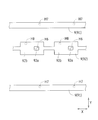
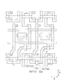
- FIG. 9 is a schematic plan view showing a layout in a state in which a semiconductor layer and a first display wiring are overlapped with each other in the display device according to the second embodiment of the present invention. It is an enlarged plan view which expands and shows the intersection area vicinity of FIG. It is a schematic cross section which shows the cross section along arrow BB of FIG.
- FIG. 1 is an equivalent circuit diagram showing a pixel circuit of a display device.
- the display device 1 has a display area composed of a plurality of pixels arranged in a matrix.
- the plurality of pixels typically includes red pixels that display red, green pixels that display green, and blue pixels that display blue.
- a corresponding light emitting diode LD is provided in each pixel and is controlled by the corresponding pixel circuit.
- a straight line corresponding to “Scan(n)” and “Scan(n ⁇ 1)” indicates a scanning signal line
- a straight line corresponding to “data” indicates a data signal line
- the straight line indicates the light emission control line.
- "ELVDD” indicates a high power supply voltage, and the straight line connected to this corresponds to the high power supply voltage line.
- “ELVSS” indicates a low power supply voltage, and the straight line connected to this corresponds to the low power supply voltage line.
- the straight line corresponding to “Vini(n)” indicates the initialization wiring corresponding to the reset potential.
- 5V is applied to the high power supply voltage line, and -5V is applied to the low power supply voltage line.
- 2 to 6V is applied to the data signal line.
- -4V is applied to the initialization wiring.
- 7V is applied to the scanning signal line and the light emission control line in the “High” state, and ⁇ 8V is applied in the “Low” state.
- FIG. 1 shows an example of a pixel circuit, which is configured by combining seven transistors (first circuit transistor T1 to seventh circuit transistor T7), a capacitor C1, and a light emitting diode LD.
- the first circuit transistor T1 to the third circuit transistor T3 and the fifth circuit transistor T5 to the seventh circuit transistor T7 are used as switching transistors.
- the fourth circuit transistor T4 is a drive transistor that supplies power to the light emitting diode LD.
- the first circuit transistor T1 is an initialization transistor, one end of which is connected to the gate electrode of the drive transistor (fourth circuit transistor T4) and the other end of which is connected to the initialization wiring.
- the seventh circuit transistor T7 is an initialization transistor, one end of which is connected to the anode of the light emitting diode LD and the other end of which is connected to the initialization wiring.
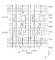
- FIG. 2 is a schematic plan view showing a pixel circuit of the display device. Note that, in FIG. 2, the wiring and the like are extracted and shown, and the interlayer insulating film and the like are shown transparently in consideration of the viewability of the drawing.
- FIG. 2 schematically shows the layout of the pixel circuit of FIG. 1 on the substrate 2, and also shows a part of the adjacent pixel circuits.
- the horizontal direction in a plan view may be referred to as the row direction X
- the vertical direction may be referred to as the column direction Y below. Note that the layout of the pixel circuit will be described in detail together with the shapes of the semiconductor layer 5, the first display wiring 7, the second display wiring 9, and the third display wiring 11 shown in FIGS.
- the second display wiring 9 includes the above-mentioned initialization wiring 91. Next, the structure in the intersection region KR near the initialization wiring 91 will be described with reference to FIGS. 3 and 4.
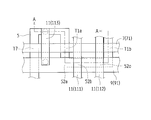
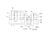
- FIG. 3 is an enlarged plan view showing the vicinity of the intersection area in FIG. 2 in an enlarged manner
- FIG. 4 is a schematic cross-sectional view showing a cross section taken along arrow AA in FIG. Note that FIG. 4 shows a state in which a cross section along the bent semiconductor layer 5 is developed in a plan view.
- the resin layer 3, the base layer 4, the semiconductor layer 5, the gate insulating film 6, the first display wiring 7, the first interlayer insulating film 8, the second display wiring 9, and the second interlayer insulating are provided on the substrate 2.
- the film 10, the third display wiring 11, and the flattening film 12 are sequentially stacked.
- the substrate 2 for example, a glass substrate, a silicon substrate, and a heat-resistant plastic substrate (resin substrate) can be used.
- a material for the plastic substrate (resin substrate) polyethylene terephthalate (PET), polyethylene naphthalate (PEN), polyether sulfone (PES), acrylic resin, polyimide, or the like can be used.
- the thickness of the substrate 2 is not particularly limited, and may be a thin film shape.
- the resin layer 3 is formed of, for example, polyimide resin (PI).
- the base layer 4 is an inorganic film formed by forming a SiO 2 film by a CVD method.
- the base layer 4 is not limited to this, and for example, silicon oxide (SiO x ), silicon nitride (SiN x ), silicon oxynitride (SiO x N y ; x>y), silicon nitride oxide (SiN x O y ; x>y), aluminum oxide, tantalum oxide, or the like, and a plurality of layers may be stacked.
- the semiconductor layer 5 is, for example, polycrystalline silicon (LTPS) formed by a known method such as a CVD method.
- LTPS polycrystalline silicon
- the semiconductor layer 5 is not limited to the above materials, but may be formed of other materials.
- the oxide semiconductor included in the semiconductor layer 5 may be, for example, an amorphous oxide semiconductor (amorphous oxide semiconductor) or a crystalline oxide semiconductor having a crystalline portion.
- Examples of the crystalline oxide semiconductor include a polycrystalline oxide semiconductor, a microcrystalline oxide semiconductor, and a crystalline oxide semiconductor in which the c-axis is oriented substantially perpendicular to the layer surface.
- the semiconductor layer 5 may have a laminated structure of two or more layers, and in this case, the semiconductor layer 5 may include an amorphous oxide semiconductor layer and a crystalline oxide semiconductor layer. .. Alternatively, it may include a plurality of crystalline oxide semiconductor layers having different crystal structures or a plurality of amorphous oxide semiconductor layers.
- the semiconductor layer 5 may include at least one metal element selected from In, Ga, and Zn, for example.
- the In-Ga-Zn-O-based semiconductor may be amorphous or crystalline.
- As the crystalline In-Ga-Zn-O-based semiconductor a crystalline In-Ga-Zn-O-based semiconductor in which the c-axis is oriented substantially perpendicular to the layer surface is preferable.
- the semiconductor layer 5 may include another oxide semiconductor instead of the In—Ga—Zn—O based semiconductor, and may include, for example, an In—Sn—Zn—O based semiconductor.
- the In—Sn—Zn—O-based semiconductor is a ternary oxide of In, Sn (tin), and Zn, and examples thereof include In 2 O 3 —SnO 2 —ZnO (InSnZnO).
- the semiconductor layer 5 is not limited to this, but an In—Al—Zn—O-based semiconductor, an In—Al—Sn—Zn—O-based semiconductor, a Zn—O-based semiconductor, an In—Zn—O-based semiconductor, a Zn—Ti—.
- O-based semiconductor Cd-Ge-O-based semiconductor, Cd-Pb-O-based semiconductor, CdO (cadmium oxide), Mg-Zn-O-based semiconductor, In-Ga-Sn-O-based semiconductor, In-Ga-O-based Semiconductor, Zr-In-Zn-O based semiconductor, Hf-In-Zn-O based semiconductor, Al-Ga-Zn-O based semiconductor, Ga-Zn-O based semiconductor, In-Ga-Zn-Sn-O based semiconductor It may contain a semiconductor, InGaO 3 (ZnO) 5 , magnesium zinc oxide (Mg X Zn 1-X O), cadmium zinc oxide (Cd X Zn 1-X O), or the like.
- ZnO magnesium zinc oxide
- Cd X Zn 1-X O magnesium zinc oxide
- Cd X Zn 1-X O cadmium zinc oxide
- an amorphous state of ZnO to which one or more impurity elements of Group 1 element, Group 13 element, Group 14 element, Group 15 element or Group 17 element is added A polycrystalline state, a microcrystalline state in which an amorphous state and a polycrystalline state are mixed, or a state in which no impurity element is added can be used.
- the gate insulating film 6 is formed of silicon oxide (SiO x ) formed by the CVD method.
- the gate insulating film 6 may be formed of the same material as the base layer 4, or may have a laminated structure in which a plurality of layers are stacked.
- the first display wiring 7 functions as a gate electrode in a transistor, is formed by a sputtering method, and is a single-layer film made of Mo.
- the first display wiring 7 is not limited to this, and for example, aluminum (Al), tungsten (W), molybdenum (Mo), tantalum (Ta), chromium (Cr), titanium (Ti), and copper (Cu).
- Al aluminum
- Mo molybdenum
- Ta tantalum
- Cr chromium
- Ti titanium
- Cu copper
- a metal film containing an element selected from the above, an alloy film containing these elements as a component, or the like may be used, or a laminated film including a plurality of these films may be used.
- the first interlayer insulating film 8, the second interlayer insulating film 10, and the flattening film 12 are formed by using the same material and method as the base layer 4.
- the second display wiring 9 and the third display wiring 11 are formed by using the same material and method as those of the first display wiring 7.
- a light emitting element or the like may be further formed on the flattening film 12, and a contact hole or the like for electrical connection may be formed.
- the semiconductor layer 5, the first display wiring 7, the second display wiring 9, and the third display wiring 11 may be appropriately formed by patterning using a known photolithography process. Further, a contact hole may be provided in an interlayer insulating film or the like to appropriately connect these different layers.
- the semiconductor layer 5 After the first display wiring 7 is molded, plasma treatment is performed to reduce the resistance. Only the portion of the semiconductor layer 5 not covered with the first display wiring 7 is processed. The resistance is lowered. The resistance of the semiconductor region 51 immediately below the first display wiring 7 is not reduced, and the exposed conductor region 52 is reduced in resistance. That is, in the semiconductor layer 5, the semiconductor region 51 immediately below the first display wiring 7 functions as a channel region in the transistor, and the conductor region 52 adjacent to the semiconductor region 51 is the source region and the drain region (conduction terminal) in the transistor. Function as. Further, a portion of the first display wiring 7 that faces the semiconductor region 51 via the gate insulating film 6 functions as a gate electrode (control terminal) in the transistor.
- the first to eighth contact holes H1 to H8 shown in FIGS. 5 to 9 show the positional relationship with the corresponding layers, and some of the unrelated layers are omitted.
- FIG. 5 is a schematic plan view showing the layout of the semiconductor layer.
- the semiconductor layer 5 has a bent shape in a plan view and is stretched around each part in the pixel circuit. As will be described later, the semiconductor layer 5 is arranged so as to overlap with the first display wiring 7, the second display wiring 9, and the third display wiring 11 which are linearly stretched, in each part in the pixel circuit. ing. The semiconductor layer 5 extends to the outside of the pixel circuit and is connected to the semiconductor layer 5 of the adjacent pixel circuit.
- FIG. 6 is a schematic plan view showing the layout of the first display wiring.
- the first display wiring 7 includes a plurality of scanning signal lines extending in the row direction X. Specifically, the first display wiring 7 has a first scanning signal line 71, a second scanning signal line 72, a drive gate portion 73, and a light emission control line 74.
- the first scanning signal line 71, the second scanning signal line 72, the drive gate unit 73, and the light emission control line 74 are arranged in the order from the lower side to the upper side. Lined up. Further, further first scanning signal lines 71 are arranged above the light emission control lines 74, and are repeatedly arranged in the above-described order.
- a first scanning signal line 71, a second scanning signal line 72, a drive gate section 73, and a light emission control line 74 are provided one by one.
- the first scanning signal line 71, the second scanning signal line 72, and the light emission control line 74 are the first scanning signal line 71, the second scanning signal line 72, and the light emission control line in the pixel circuits that are adjacent in the row direction X. 74, respectively.
- the first scanning signal line 71 has a linear shape that passes through the above-mentioned intersection region KR.
- the second scanning signal line 72 has a substantially linear shape, and has a branch extending portion 72 a that branches and extends in the column direction Y.
- the drive gate portion 73 has a rectangular shape. The shape of the drive gate portion 73 is not limited to this, and may be appropriately modified according to the shape of the semiconductor layer 5 to be overlapped.
- the light emission control line 74 has a linear shape.
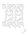
- FIG. 7 is a schematic plan view showing a layout in which the semiconductor layer and the first display wiring are superposed on each other.
- the semiconductor layer 5 is divided into the conductor region 52 and the semiconductor region 51 depending on whether or not it overlaps with the first display wiring 7.
- the range surrounded by the alternate long and short dash line corresponds to one pixel circuit GS.
- the first scanning signal line 71 and the semiconductor layer 5 have three overlapping portions in one pixel circuit GS.
- the semiconductor layer 5 in the intersection region KR is formed in a substantially S shape by combining a portion extended in the row direction X and a portion extended in the column direction Y, and extends in the row direction X.
- the formed first scanning signal lines 71 intersect at three positions separated in the row direction X.
- first transistor T1a and second transistor T1b correspond to the first circuit transistor T1 and one location corresponds to the seventh circuit transistor T7.
- the first circuit transistor T1 is a double gate type transistor by combining the first transistor T1a and the second transistor T1b connected in the conductor region 52.
- the conductor region 52 that connects the first transistor T1a and the second transistor T1b may be referred to as a connecting portion 52a.
- the first transistor T1a and the seventh circuit transistor T7 of the pixel circuit GS adjacent in the row direction X are connected by the conductor region 52 and overlap the first contact hole H1.
- the second scanning signal line 72 is superposed on the semiconductor layer 5 in one pixel circuit GS at two places in the straight line portion and one place in the branch extending portion 72a.
- One of the second scanning signal lines 72 that overlaps the semiconductor layer 5 in the straight line portion corresponds to the third circuit transistor T3, and the other (drive gate in FIG. 7).
- the lower right of the portion 73) corresponds to the second circuit transistor T2 (straight line overlapping portion T2a).
- the portion of the second scanning signal line 72 that overlaps the semiconductor layer 5 in the branch extending portion 72a also corresponds to the second circuit transistor T2 (branch overlapping portion T2b).
- the straight line overlapping portion T2a and the branch overlapping portion T2b are connected by a conductor region 52. That is, the second circuit transistor T2 is configured as a combination of the straight line overlapping portion T2a and the branch overlapping portion T2b, similarly to the first circuit transistor T1, and is a double gate type transistor.
- the conductor region 52 connects between the second transistor T1b and the branch overlapping portion T2b, and overlaps with the third contact hole H3.
- the conductor region 52 (downward in FIG. 7) extending from the third circuit transistor T3 has a tip that overlaps with the second contact hole H2.
- the drive gate portion 73 is superposed at one location on the semiconductor layer 5 in one pixel circuit GS and corresponds to the fourth circuit transistor T4.
- the sixth contact hole H6 overlaps the drive gate portion 73.
- the light emission control line 74 is overlapped at two positions with respect to the semiconductor layer 5 in one pixel circuit, and the fifth circuit transistor T5 (upper left of the drive gate portion 73 in FIG. 7) and the sixth circuit transistor T6 ( In FIG. 7, it corresponds to the upper right of the drive gate portion 73).
- the tip of the conductor region 52 (upper side in FIG. 7) extending from the fifth circuit transistor T5 overlaps the fourth contact hole H4.
- the conductor region 52 (upper side in FIG. 7) extending from the sixth circuit transistor T6 is located higher in FIG. 7 and is connected to the seventh circuit transistor T7 of the pixel circuit GS adjacent in the column direction Y, It overlaps with the fifth contact hole H5.
- the conductor region 52 extending from the fourth circuit transistor T4 to one side is branched into two and is connected to the third circuit transistor T3 and the fifth circuit transistor T5. Further, the conductor region 52 extending from the fourth circuit transistor T4 to the other side (to the right in FIG. 7) is branched into two, and the second circuit transistor T2 (straight line overlapping portion T2a) and the sixth circuit transistor T6 It is connected to the.
- FIG. 8 is a schematic plan view showing the layout of the second display wiring.
- the second display wiring 9 includes a constant potential wiring extending in the row direction X. Specifically, the second display wiring 9 has an initialization wiring 91 and a first high power supply voltage line 92.
- the initialization wiring 91 and the first high power supply voltage line 92 are arranged in order from the bottom to the top. That is, the initialization wiring 91 and the first high power supply voltage line 92 are alternately and repeatedly arranged.
- one initialization wiring line 91 and one first high power supply voltage line 92 are provided in each pixel circuit.
- the initialization wiring 91 and the first high power supply voltage line 92 are connected to the initialization wiring 91 and the first high power supply voltage line 92 in the pixel circuits adjacent to each other in the row direction X, respectively.
- the initialization wiring 91 has a linear shape passing through the above-described intersection region KR and passes through a position aligned with the first scanning signal line 71 in the column direction Y.
- the seventh contact hole H7 overlaps the initialization wiring 91 in the vicinity of the first contact hole H1.
- the first high power supply voltage line 92 passes through the position overlapping the drive gate portion 73 described above, and has a substantially straight shape with a part of the width being widened.
- the wide portion 92b having the wide width is sized to cover substantially the entire drive gate portion 73.
- the wide portion 92b is provided with an opening 92a that is partially open, and the first display wiring 7 is not covered with the second display wiring 9 in the opening 92a.
- the opening 92a is provided at a position overlapping the sixth contact hole H6.
- the third display wiring 11 is embedded in the sixth contact hole H6, and the first display wiring 7 and the third display wiring 11 are connected via the sixth contact hole H6.
- the eighth contact hole H8 overlaps the wide portion 92b in the vicinity of the fourth contact hole H4.
- FIG. 9 is a schematic plan view showing the layout of the third display wiring.
- the third display wiring 11 includes a data signal line 111 extending in the column direction Y. Specifically, the third display wiring 11 has a data signal line 111, a second high power supply voltage line 112, and a contact connection portion (initialization connection portion 113, drive connection portion 114, and light emission connection portion 115). There is.
- the data signal line 111, the second high power supply voltage line 112, and the contact connection part are arranged in order from the left to the right. Further, the further data signal line 111 is arranged on the right side of the contact connecting portion, and is repeatedly arranged in the order described above.
- a data signal line 111, a second high power supply voltage line 112, and a contact connection section are provided in each pixel circuit. Further, in the contact connection part, the initialization connection part 113, the drive connection part 114, and the light emission connection part 115 are provided at positions separated in the column direction Y, respectively.
- the data signal line 111 has a linear shape passing through the above-mentioned intersection region KR and is arranged at a position passing through the second contact hole H2 and the connecting portion 52a.
- the portion of the connecting portion 52a that overlaps the data signal line 111 may be referred to as the overlapping connecting portion 52b below.
- the overlapping connection portion 52b overlaps the initialization wiring 91 in a plan view.
- the initialization wiring 91 be overlapped with the entire portion including the end portion of the overlapping coupling portion 52b so as to cover the overlapping coupling portion 52b. That is, it is preferable that, of the connecting portions 52a, all the overlapping connecting portions 52b that overlap with the data signal line 111 in a plan view overlap with the constant potential wiring (initializing wiring 91) in a plan view.
- the second high power supply voltage line 112 has a linear shape passing through the above-mentioned intersection region KR and is arranged at a position passing through the fourth contact hole H4, the eighth contact hole H8, and the connecting portion 52a.
- the initialization connection portion 113 is provided so as to connect the first contact hole H1 to the seventh contact hole H7. That is, the conductor region 52 near the first transistor T1a and the initialization wiring 91 are electrically connected via the initialization connection unit 113.
- the drive connection portion 114 is provided so as to connect the third contact hole H3 to the sixth contact hole H6. That is, the conductor region 52 near the second transistor T1b and the drive gate portion 73 are electrically connected via the drive connection portion 114.
- the light emitting connection portion 115 is provided at a position overlapping the fifth contact hole H5, and is electrically connected to the light emitting diode LD described above.
- One conduction terminal (the conductor region 52 below the first transistor T1a in FIG. 3) and the other conduction terminal (the conductor region 52 above the first transistor T1a in FIG. 3) of the first transistor T1a are data They are arranged in the column direction Y along the signal line 111.
- One conduction terminal (the conductor region 52 below the second transistor T1b in FIG. 3) and the other conduction terminal (the conductor region 52 above the second transistor T1b in FIG. 3) of the second transistor T1b are the data.
- the signal lines 111 are arranged in the column direction.
- the connecting portion 52a overlaps the constant potential wiring (initialization wiring 91) and extends in the row direction X.
- One conduction terminal of the first transistor T1a and one conduction terminal of the second transistor T1b are connected via the coupling portion 52a.
- the data signal line 111 passes between the first transistor T1a and the second transistor T1b in the row direction X, and intersects with the initialization wiring 91 at a portion overlapping the overlapping connection portion 52b in a plan view.
- the constant potential wiring (initialization wiring 91) is sandwiched between the data signal line 111 and the conductor region 52 (superimposed connection portion 52b) so that the data signal line 111 and the conductor region 52 intersect (superimpose).
- the influence on the conductor region 52 can be prevented, and the operation of the transistor can be stabilized. That is, when the data signal line 111 and the conductor region 52 are overlapped with each other, the parasitic capacitance between them may affect the operation of the transistor, but a constant potential wiring to which a constant potential is applied is sandwiched therebetween. Therefore, the fluctuation of the potential can be suppressed.
- the scanning signal line overlapping the first transistor T1a and the scanning signal line overlapping the second transistor T1b are the same first scanning signal line 71, and the same signal is applied. In this manner, by driving the first transistor T1a and the second transistor T1b which are provided in succession with the same signal, it is possible to function as a dual-gate transistor.
- the first signal transistor T1a and the second signal transistor T1b are prevented from overlapping the data signal line 111, and the data signal line 111 intersects at the overlapping connection portion 52b covered by the initialization wiring 91. be able to. That is, the restriction on the arrangement of the semiconductor layer 5 with respect to the data signal line 111 is relaxed, so that the degree of freedom of layout in the display device 1 can be improved. Further, by providing the initialization wiring 91 for resetting the potential of the transistor, the transistor can be operated in various ways.
- the second high power supply voltage line 112 also has a wiring overlapping portion 52c that overlaps the connecting portion 52a in plan view, and the wiring overlapping portion 52c overlaps the initialization wiring 91. You may have. Further, it is preferable that the initialization wiring 91 be overlapped with the whole including the end portion of the wiring overlapping portion 52c so as to cover the wiring overlapping portion 52c. That is, it is preferable that all the wiring overlapping portions 52c of the connecting portion 52a, including the end portions, overlap the constant potential wiring (initialization wiring 91) in a plan view. As a result, the influence of the parasitic capacitance with the second high power supply voltage line 112 can be suppressed.
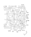
- FIG. 10 is a schematic plan view showing a pixel circuit of a display device according to a second embodiment of the present invention
- FIG. 11 shows a semiconductor layer and a first display in the display device according to the second embodiment of the present invention
- FIG. 13 is a schematic plan view showing a layout in the state of being overlapped with wiring
- FIG. 12 is an enlarged plan view showing the vicinity of the intersection area of FIG. 10 in an enlarged manner
- FIG. 13 is an arrow mark of FIG.
- It is a schematic cross section which shows the cross section in BB. Note that, in FIGS. 10 and 11, the wiring and the like are extracted and shown, and the interlayer insulating film and the like are transparently shown in consideration of the visibility of the drawings. Further, FIG. 13 shows a state in which a cross section along the bent semiconductor layer 5 in a plan view is developed.
- the second embodiment is different from the first embodiment in the structure in the intersection region KR.
- the first scanning signal line 71 of the first display wiring 7 has a branch gate electrode 71 a that is substantially linear and branches and extends in the column direction Y. ..
- the branch gate electrode 71a is located between the data signal line 111 and the second high power supply voltage line 112 in the row direction X, and overlaps a part of the semiconductor layer 5.
- a portion of the semiconductor layer 5 that overlaps the branch gate electrode 71a is a semiconductor region 51, which functions as the third transistor T1c.
- one conduction terminal in FIG. 12, the conductor region 52 on the left side of the third transistor T1c has one conduction terminal of the first transistor (see FIG. 12) via the coupling portion 52a. Is connected to the conductor region 52) below the first transistor T1a, and the other conduction terminal (in FIG. 12, the conductor region 52 on the right side of the third transistor T1c) is connected to the second transistor via the connecting portion 52a. It is connected to one conduction terminal (in FIG. 12, the conductor region 52 below the second transistor T1b).
- the third transistor T1c By providing and combining the third transistor T1c connected via the conductor region 52 between the first transistor T1a and the second transistor T1b, it is possible to function as one triple gate type transistor.
- the first transistor T1a, the second transistor T1b, and the third transistor T1c correspond to the first circuit transistor T1 in the pixel circuit GS.
- the display device 1 is not particularly limited as long as it is a display panel including a display element.
- the display element includes a display element whose luminance and transmittance are controlled by current and a display element whose luminance and transmittance are controlled by voltage.
- Examples of the current-controlled display element include an organic EL (Electro Luminescence) display including an OLED (Organic Light Emitting Diode), an inorganic EL display including an inorganic light emitting diode, and the like.
- OLED Organic Light Emitting Diode
- an inorganic EL display including an inorganic light emitting diode, and the like.
- As the voltage-controlled display element there is a liquid crystal display element or the like.
- first display wiring 71 first scanning signal line (an example of scanning signal line) 72 Second scan signal line (an example of scan signal line) 73 drive gate section 74 light emission control line 8 first interlayer insulating film 9 second display wiring 91 initialization wiring (an example of constant potential line) 92 First high power voltage line (an example of constant potential line) 10 Second Interlayer Insulating Film 11 Third Display Wiring 111 Data Signal Line 112 Second High Power Supply Voltage Line GS Pixel Circuit T1a First Transistor T1b Second Transistor T1c Third Transistor X Row Direction Y Column Direction
Landscapes
- Engineering & Computer Science (AREA)
- Microelectronics & Electronic Packaging (AREA)
- Physics & Mathematics (AREA)
- General Physics & Mathematics (AREA)
- Theoretical Computer Science (AREA)
- Devices For Indicating Variable Information By Combining Individual Elements (AREA)
- Electroluminescent Light Sources (AREA)
Abstract
表示装置(1)では、基板(2)上に、半導体層(5)、ゲート絶縁膜(6)、第1表示配線(7)、第1層間絶縁膜(8)、第2表示配線(9)、第2層間絶縁膜(10)、および第3表示配線(11)が順に積層されている。画素回路(GS)は、半導体層(5)と走査信号線(71)とが重畳する第1トランジスタ(T1a)および第2トランジスタ(T1b)を有する。第1トランジスタ(T1a)と第2トランジスタ(T1b)とは、半導体層(5)の導体領域(52)における連結部(52a)を介して接続されている。連結部(52a)は、第2表示配線(9)を介して、第3表示配線(11)と平面視で重畳する重畳連結部(52b)を含む。
Description
本発明は、基板上に形成される表示デバイスの製造方法および表示デバイスに関する。
近年、OLED(Organic Light Emitting Diode)技術の進歩に伴い、有機EL(エレクトロルミネッセンス)表示装置を備えた製品が広がってきている。一般に、有機EL表示装置では、発光層における画素に電流を供給する複数の画素回路を含む構成を用いられている。
画素回路は、通常、複数のトランジスタを組み合わせて構成されており、入力される信号に応じて、発光させる画素を適宜選択している。ところで、トランジスタの配置によっては、ゲート電極への電荷の蓄積などによって、意図しないリーク電流が発光素子に流れ、画素の輝度が制御できないことがあった。そこで、トランジスタをダブルゲート構造にして、リーク電流を抑制する技術が提案されている(例えば、特許文献1参照)。
特許文献1に記載の表示装置では、基板上に2つの薄膜トランジスタを設けており、一方の薄膜トランジスタは、ダブルゲート構造を有している。上述した表示装置では、2つのトランジスタを組み合わせて画素回路を構成しているが、さらに、トランジスタを増やして、細密な制御を行うことが考慮されていない。また、トランジスタを増やすと、それらに対する配線が複雑化し、小さな領域に収めるようにレイアウトすることが困難になるという課題がある。
本発明は、上記の課題を解決するためになされたものであり、トランジスタの動作を安定させることができる表示装置を提供することを目的とする。
本発明に係る表示装置は、表示パネルに配置された複数の画素回路に、それぞれデータ信号を供給することによって画像を表示する表示装置であって、基板上に順に積層された半導体層、ゲート絶縁膜、第1表示配線、第1層間絶縁膜、第2表示配線、第2層間絶縁膜、および第3表示配線とを備え、前記第1表示配線は、行方向に延伸された複数の走査信号線を含み、前記第2表示配線は、前記行方向に延伸された複数の定電位配線を含み、前記第3表示配線は、前記行方向と交差する列方向に延伸され、前記走査信号線および前記定電位配線と交差する複数のデータ信号線を含み、前記複数の画素回路は、前記複数のデータ信号線と前記複数の走査信号線との交点に対応して設けられ、前記画素回路は、前記複数の走査信号線のうちのいずれかの走査信号線と前記半導体層とが、前記ゲート絶縁膜を介して重畳する第1トランジスタおよび第2トランジスタを有し、前記第1トランジスタの一方の導通端子と、前記第2トランジスタの一方の導通端子とは、前記半導体層の導体領域に含まれる連結部を介して接続され、前記連結部は、前記定電位配線を介して、前記データ信号線と平面視で重畳する重畳連結部を含むことを特徴とする。
本発明に係る表示装置では、前記第1トランジスタの一方の導通端子と他方の導通端子とは、前記データ信号線に沿って、前記列方向に並び、前記第2トランジスタの一方の導通端子と他方の導通端子とは、前記データ信号線に沿って、前記列方向に並び、前記重畳連結部は、前記定電位配線と重畳し、前記行方向に延伸されている構成としてもよい。
本発明に係る表示装置では、前記定電位配線のうちいずれか1つは、初期化配線とされている構成としてもよい。
本発明に係る表示装置では、前記第1トランジスタおよび前記第2トランジスタは、初期化トランジスタとされている構成としてもよい。
本発明に係る表示装置では、前記画素回路は、駆動トランジスタを有し、前記第1トランジスタの他方の導通端子は、前記初期化配線と電気的に接続され、前記第2トランジスタの他方の導通端子は、前記駆動トランジスタの制御端子と電気的に接続されている構成としてもよい。
本発明に係る表示装置では、前記画素回路は、前記第1トランジスタおよび前記第2トランジスタに対して重畳する走査信号線から分岐して延伸された分岐ゲート電極と、前記半導体層とが重畳する第3トランジスタを有する構成としてもよい。
本発明に係る表示装置では、前記第3トランジスタは、一方の導通端子が、前記連結部を介して前記第1トランジスタの一方の導通端子と接続され、他方の導通端子が、前記連結部を介して前記第2トランジスタの一方の導通端子と接続されている構成としてもよい。
本発明に係る表示装置では、前記第3トランジスタの半導体層は、前記定電位配線と平面視で重畳する構成としてもよい。
本発明に係る表示装置では、前記データ信号線は、前記行方向での前記第1トランジスタと前記第3トランジスタとの間を通る構成としてもよい。
本発明に係る表示装置では、前記第3表示配線は、電源電圧線を含み、前記電源電圧線は、前記行方向での前記第2トランジスタと前記第3トランジスタとの間を通る構成としてもよい。
本発明に係る表示装置では、前記第1トランジスタの他方の導通端子は、隣接する画素回路の初期化トランジスタのいずれかの導通端子に対して、前記半導体層の導体領域を介して接続されている構成としてもよい。
本発明に係る表示装置では、前記走査信号線は、発光制御線を含む構成としてもよい。
本発明によると、この構成によると、データ信号線と導体領域との間に、定電位配線を挟んで交差(重畳)させることで、データ信号線から導体領域に与える影響を防ぐことができ、トランジスタの動作を安定させることができる。
(第1実施形態)
以下、本発明の第1実施形態に係る表示装置について、図面を参照して説明する。
以下、本発明の第1実施形態に係る表示装置について、図面を参照して説明する。
図1は、表示装置の画素回路を示す等価回路図である。
表示装置1は、マトリクス状に配列された複数の画素によって構成された表示領域を有する。複数の画素は、典型的には、赤を表示する赤画素、緑を表示する緑画素、および青を表示する青画素を含む。それぞれの画素では、対応する発光ダイオードLDが設けられており、対応する画素回路によって制御している。
「Scan(n)」および「Scan(n-1)」に対応する直線は、走査信号線を示し、「data」に対応する直線は、データ信号線を示し、「em(n)」に対応する直線は、発光制御線を示している。また、「ELVDD」は、高電源電圧を示し、これに繋がる直線は、高電源電圧線に相当する。さらに、「ELVSS」は、低電源電圧を示し、これに繋がる直線は、低電源電圧線に相当する。そして、「Vini(n)」に対応する直線は、リセット電位に対応する初期化配線を示している。
本実施の形態において、高電源電圧線には、5Vが印加され、低電源電圧線には、-5Vが印加される。データ信号線には、2~6Vが印加される。初期化配線には、-4Vが印加される。走査信号線および発光制御線には、「High」とされた状態において7Vが印加され、「Low」とされた状態において-8Vが印加される。
図1は、画素回路の一例を示しており、7つのトランジスタ(第1回路トランジスタT1ないし第7回路トランジスタT7)、コンデンサC1、および発光ダイオードLDを組み合わせて構成されている。
画素回路において、第1回路トランジスタT1ないし第3回路トランジスタT3と、第5回路トランジスタT5ないし第7回路トランジスタT7とは、スイッチングトランジスタとして用いられている。また、第4回路トランジスタT4は、発光ダイオードLDに電源を供給する駆動トランジスタとされている。
第1回路トランジスタT1は、初期化トランジスタとされ、一端が駆動トランジスタ(第4回路トランジスタT4)のゲート電極に接続され、他端が初期化配線に接続されている。また、第7回路トランジスタT7は、初期化トランジスタとされ、一端が発光ダイオードLDのアノードに接続され、他端が初期化配線に接続されている。
図2は、表示装置の画素回路を示す概略平面図である。なお、図2では、図面の見易さを考慮して、配線などを抽出して示し、層間絶縁膜等を透視的に示している。
図2は、図1の画素回路について、基板2上でのレイアウトを模式的に示しており、隣接する画素回路の一部も併せて示している。以下では説明のため、平面視した状態での横方向を行方向Xと呼び、縦方向を列方向Yと呼ぶことがある。なお、画素回路のレイアウトについては、図5ないし図9に示す半導体層5、第1表示配線7、第2表示配線9、および第3表示配線11の形状と併せて、詳細に説明する。
第2表示配線9は、上述した初期化配線91を含んでいる。次に、初期化配線91近傍の交差領域KRでの構造について、図3および図4を参照して説明する。
図3は、図2の交差領域近傍を拡大して示す拡大平面図であって、図4は、図3の矢符A-Aでの断面を示す模式断面図である。なお、図4は、平面視において屈曲した半導体層5に沿った断面を展開した状態を示している。
表示装置1では、基板2上に、樹脂層3、下地層4、半導体層5、ゲート絶縁膜6、第1表示配線7、第1層間絶縁膜8、第2表示配線9、第2層間絶縁膜10、第3表示配線11、および平坦化膜12が順に積層されている。
基板2としては、例えば、ガラス基板、シリコン基板、および耐熱性を有するプラスチック基板(樹脂基板)を用いることができる。プラスチック基板(樹脂基板)の材料としては、ポリエチレンテレフタレート(PET)、ポリエチレンナフタレート(PEN)、ポリエーテルサルフォン(PES)、アクリル樹脂、およびポリイミド等を用いることができる。なお、基板2の厚みは特に限定されず、薄いフィルム状であってもよい。
樹脂層3は、例えば、ポリイミド樹脂(PI)などで形成されている。
下地層4は、SiO2膜をCVD法によって成膜した無機膜である。下地層4は、これに限定されず、例えば、酸化珪素(SiOx)、窒化珪素(SiNx)、酸化窒化珪素(SiOxNy;x>y)、窒化酸化珪素(SiNxOy;x>y)、酸化アルミニウム、および酸化タンタルなどで形成されていてもよく、複数の層を積層してもよい。
半導体層5は、例えば、CVD法などの周知の方法で形成された多結晶シリコン(LTPS)とされている。
なお、半導体層5については、上述した材料だけに限らず、他の材料によって形成してもよい。半導体層5に含まれる酸化物半導体は、例えば、アモルファス酸化物半導体(非晶質酸化物半導体)であってもよいし、結晶質部分を有する結晶質酸化物半導体であってもよい。結晶質酸化物半導体としては、多結晶酸化物半導体、微結晶酸化物半導体、およびc軸が層面に概ね垂直に配向した結晶質酸化物半導体などが挙げられる。
また、半導体層5は、2層以上の積層構造を有していてもよく、この場合、半導体層5は、非晶質酸化物半導体層と結晶質酸化物半導体層とを含んでいてもよい。あるいは、結晶構造が異なる複数の結晶質酸化物半導体層を含んでいてもよいし、複数の非晶質酸化物半導体層を含んでいてもよい。
次に、非晶質酸化物半導体および結晶質酸化物半導体の材料や構造などについて、詳細に説明する。半導体層5は、例えば、In、Ga、およびZnのうち、少なくとも1種の金属元素を含んでいてもよい。ここで、In-Ga-Zn-O系の半導体は、In(インジウム)、Ga(ガリウム)、およびZn(亜鉛)の三元系酸化物であって、In、Ga、およびZnの割合(組成比)は、特に限定されず、例えば、In:Ga:Zn=2:2:1、In:Ga:Zn=1:1:1、およびIn:Ga:Zn=1:1:2等を含む。また、In-Ga-Zn-O系の半導体は、アモルファスでもよいし、結晶質でもよい。結晶質In-Ga-Zn-O系の半導体としては、c軸が層面に概ね垂直に配向した結晶質In-Ga-Zn-O系の半導体が好ましい。
半導体層5は、In-Ga-Zn-O系半導体の換わりに、他の酸化物半導体を含んでいてもよく、例えば、In-Sn-Zn-O系半導体を含んでいてもよい。In-Sn-Zn-O系の半導体は、In、Sn(スズ)、およびZnの三元系酸化物であって、例えば、In2O3-SnO2-ZnO(InSnZnO)などが挙げられる。
半導体層5は、これに限らず、In-Al-Zn-O系半導体、In-Al-Sn-Zn-O系半導体、Zn-O系半導体、In-Zn-O系半導体、Zn-Ti-O系半導体、Cd-Ge-O系半導体、Cd-Pb-O系半導体、CdO(酸化カドミウム)、Mg-Zn-O系半導体、In-Ga-Sn-O系半導体、In-Ga-O系半導体、Zr-In-Zn-O系半導体、Hf-In-Zn-O系半導体、Al-Ga-Zn-O系半導体、Ga-Zn-O系半導体、In-Ga-Zn-Sn-O系半導体、InGaO3(ZnO)5、酸化マグネシウム亜鉛(MgXZn1-XO)、および酸化カドミウム亜鉛(CdXZn1-XO)などを含んでいてもよい。Zn-O系半導体としては、1族元素、13族元素、14族元素、15族元素または17族元素のうち一種、または複数種の不純物元素が添加されたZnOの非晶質(アモルファス)状態、多結晶状態または非晶質状態と多結晶状態が混在する微結晶状態のもの、または何も不純物元素が添加されていないものを用いることができる。
ゲート絶縁膜6は、CVD法を用いて成膜された酸化珪素(SiOx)で形成されている。ゲート絶縁膜6は、下地層4と同じ材料で形成してもよく、複数の層を重ねた積層構造とされていてもよい。
第1表示配線7は、トランジスタにおけるゲート電極として機能し、スパッタリング法を用いて成膜され、Moで形成された単層膜とされている。第1表示配線7は、これに限定されず、例えば、アルミニウム(Al)、タングステン(W)、モリブデン(Mo)、タンタル(Ta)、クロム(Cr)、チタン(Ti)、および銅(Cu)から選ばれた元素を含む金属膜、またはこれらの元素を成分とする合金膜などを用いてもよいし、これらのうちの複数の膜を含む積層膜を用いてもよい。
第1層間絶縁膜8、第2層間絶縁膜10、および平坦化膜12は、下地層4と同様の材料および方法で形成される。また、第2表示配線9および第3表示配線11は、第1表示配線7と同様の材料および方法で形成される。なお、平坦化膜12の上には、さらに発光素子などを形成してもよく、電気的に接続するためのコンタクトホールなどを形成してもよい。
半導体層5、第1表示配線7、第2表示配線9、および第3表示配線11は、公知のフォトリソグラフィプロセスを用いたパターニングによって、適宜成形すればよい。また、層間絶縁膜等にコンタクトホールを設けて、これらの異なる層を適宜接続してもよい。
半導体層5に対しては、第1表示配線7を成型した後、プラズマ処理を施して低抵抗化を行っており、半導体層5のうち、第1表示配線7で覆われていない部分のみが低抵抗化される。そして、第1表示配線7の直下の半導体領域51は、低抵抗化されず、露出している導体領域52は低抵抗化される。つまり、半導体層5では、第1表示配線7の直下の半導体領域51が、トランジスタにおけるチャネル領域として機能し、半導体領域51に隣接する導体領域52が、トランジスタにおけるソース領域およびドレイン領域(導通端子)として機能する。また、第1表示配線7のうち、ゲート絶縁膜6を介して半導体領域51に対向する部分が、トランジスタにおけるゲート電極(制御端子)として機能する。
次に、平面視した状態での各層の形状について、図5ないし図9を参照して説明する。なお、図5ないし図9に示す第1コンタクトホールH1ないし第8コンタクトホールH8は、対応する層との位置関係を示すものであり、関連しない層に対しては、一部省略している。
図5は、半導体層のレイアウトを示す概略平面図である。
半導体層5は、平面視において屈曲した形状とされ、画素回路内の各部に張り巡らされている。後述するように、直線状に延伸された第1表示配線7、第2表示配線9、および第3表示配線11に対して、画素回路内の各部で重畳するように、半導体層5が配置されている。また、半導体層5は、画素回路の外部へ延伸されており、隣接する画素回路の半導体層5と接続されている。
図6は、第1表示配線のレイアウトを示す概略平面図である。
第1表示配線7は、行方向Xに延伸された複数の走査信号線を含む。具体的に、第1表示配線7は、第1走査信号線71、第2走査信号線72、駆動ゲート部73、および発光制御線74を有している。図6において、最も下方の第1走査信号線71を基準にすると、下方から上方へ向かう順に、第1走査信号線71、第2走査信号線72、駆動ゲート部73、および発光制御線74が並んでいる。そして、発光制御線74の上方には、さらなる第1走査信号線71が配置されており、上述した順で繰り返し配置されている。1つの画素回路内には、第1走査信号線71、第2走査信号線72、駆動ゲート部73、および発光制御線74が1つずつ設けられている。また、第1走査信号線71、第2走査信号線72、および発光制御線74は、行方向Xで隣接する画素回路における第1走査信号線71、第2走査信号線72、および発光制御線74と、それぞれ接続されている。
第1走査信号線71は、上述した交差領域KRを通る直線状とされている。第2走査信号線72は、略直線状とされ、分岐して列方向Yに延伸された分岐延伸部72aを有している。駆動ゲート部73は、矩形状とされている。なお、駆動ゲート部73の形状は、これに限定されず、重畳する半導体層5の形状に応じて、適宜変形してもよい。発光制御線74は、直線状とされている。
図7は、半導体層と第1表示配線とを重ね合わせた状態でのレイアウトを示す概略平面図である。
上述したように、第1表示配線7と重なっているかどうかによって、半導体層5は、導体領域52と半導体領域51とに分けられる。なお、図7において、一点鎖線で囲まれた範囲が、1つの画素回路GSに対応している。第1走査信号線71と半導体層5とは、1つの画素回路GS内で、重畳している部分が3箇所ある。具体的に、交差領域KRにおける半導体層5は、行方向Xに延伸された部分と列方向Yに延伸された部分とを組み合わせて、略S字状に成形されており、行方向Xに延伸された第1走査信号線71に対して、行方向Xで離間した3箇所で交差する。
3箇所の導体領域52のうち、2箇所(第1トランジスタT1aおよび第2トランジスタT1b)は第1回路トランジスタT1に対応し、1箇所は第7回路トランジスタT7に対応している。第1回路トランジスタT1は、導体領域52で接続された第1トランジスタT1aと第2トランジスタT1bとを組み合わせて、ダブルゲート方式のトランジスタとされている。以下では説明のため、第1トランジスタT1aと第2トランジスタT1bとの間を接続する導体領域52を連結部52aと呼ぶことがある。また、第1トランジスタT1aと、行方向Xで隣接する画素回路GSの第7回路トランジスタT7との間は、導体領域52で接続されており、第1コンタクトホールH1と重畳する。
第2走査信号線72は、1つの画素回路GS内で半導体層5に対して、直線部において2箇所が重畳し、分岐延伸部72aにおいて1箇所が重畳している。第2走査信号線72のうち、直線部において半導体層5に重畳する一方(図7では、駆動ゲート部73の左下)は、第3回路トランジスタT3に対応し、他方(図7では、駆動ゲート部73の右下)は、第2回路トランジスタT2(直線重畳部T2a)に対応する。また、第2走査信号線72のうち、分岐延伸部72aにおいて半導体層5に重畳する箇所も、第2回路トランジスタT2(分岐重畳部T2b)に対応する。直線重畳部T2aと分岐重畳部T2bとの間は、導体領域52で接続されている。つまり、第2回路トランジスタT2は、第1回路トランジスタT1と同様に、直線重畳部T2aと分岐重畳部T2bとを組み合わせた構成とされ、ダブルゲート方式のトランジスタとされている。第2トランジスタT1bと分岐重畳部T2bとの間は、導体領域52で接続されており、第3コンタクトホールH3と重畳する。第3回路トランジスタT3から延伸された導体領域52(図7では、下方)は、先端が第2コンタクトホールH2と重畳する。
駆動ゲート部73は、1つの画素回路GS内で半導体層5に対して1箇所が重畳し、第4回路トランジスタT4に対応する。第6コンタクトホールH6は、駆動ゲート部73と重畳する。
発光制御線74は、1つの画素回路内で半導体層5に対して2箇所が重畳し、それぞれ第5回路トランジスタT5(図7では、駆動ゲート部73の左上)と、第6回路トランジスタT6(図7では、駆動ゲート部73の右上)とに対応する。第5回路トランジスタT5から延伸された導体領域52(図7では、上方)は、先端が第4コンタクトホールH4と重畳する。第6回路トランジスタT6から延伸された導体領域52(図7では、上方)は、図7において上方に位置し、列方向Yで隣接する画素回路GSの第7回路トランジスタT7と接続されており、第5コンタクトホールH5と重畳する。
第4回路トランジスタT4から一方(図7では、左方)に延伸された導体領域52は、2つに分岐し、第3回路トランジスタT3と第5回路トランジスタT5とに接続されている。また、第4回路トランジスタT4から他方(図7では、右方)に延伸された導体領域52は、2つに分岐し、第2回路トランジスタT2(直線重畳部T2a)と第6回路トランジスタT6とに接続されている。
図8は、第2表示配線のレイアウトを示す概略平面図である。
第2表示配線9は、行方向Xに延伸された定電位配線を含む。具体的に、第2表示配線9は、初期化配線91および第1高電源電圧線92を有している。図8において、最も下方の初期化配線91を基準にすると、下方から上方へ向かう順に、初期化配線91および第1高電源電圧線92が並んでいる。つまり、初期化配線91と第1高電源電圧線92とが交互に繰り返して配置されている。1つの画素回路内には、初期化配線91および第1高電源電圧線92が1つずつ設けられている。また、初期化配線91および第1高電源電圧線92は、行方向Xで隣接する画素回路における初期化配線91および第1高電源電圧線92と、それぞれ接続されている。
初期化配線91は、上述した交差領域KRを通る直線状とされ、第1走査信号線71と列方向Yで並んだ位置を通る。第7コンタクトホールH7は、第1コンタクトホールH1の近傍において、初期化配線91と重畳する。
第1高電源電圧線92は、上述した駆動ゲート部73と重畳する位置を通り、一部の幅が広くなった略直線状とされている。具体的に、第1高電源電圧線92において、幅が広くなっている幅広部92bは、駆動ゲート部73の略全体を覆う大きさとされている。幅広部92bには、一部を開口した開口部92aが設けられており、開口部92aでは、第1表示配線7が第2表示配線9に覆われていない。また、開口部92aは、第6コンタクトホールH6と重畳する位置に設けられている。第6コンタクトホールH6には、第3表示配線11が埋め込まれており、第6コンタクトホールH6を介して、第1表示配線7と第3表示配線11とが接続されている。第8コンタクトホールH8は、第4コンタクトホールH4の近傍において、幅広部92bと重畳する。
図9は、第3表示配線のレイアウトを示す概略平面図である。
第3表示配線11は、列方向Yに延伸されたデータ信号線111を含む。具体的に、第3表示配線11は、データ信号線111、第2高電源電圧線112、およびコンタクト接続部(初期化接続部113、駆動接続部114、および発光接続部115)を有している。
図9において、最も左方のデータ信号線111を基準にすると、左方から右方へ向かう順に、データ信号線111、第2高電源電圧線112、およびコンタクト接続部が並んでいる。そして、コンタクト接続部の右方には、さらなるデータ信号線111が配置されており、上述した順で繰り返し配置されている。1つの画素回路内には、データ信号線111、第2高電源電圧線112、およびコンタクト接続部が1つずつ設けられている。また、コンタクト接続部において、初期化接続部113、駆動接続部114、および発光接続部115は、それぞれ列方向Yで離間した位置に設けられている。
データ信号線111は、上述した交差領域KRを通る直線状とされ、第2コンタクトホールH2および連結部52aを通る位置に配置されている。なお、以下では説明のため、連結部52aのうち、データ信号線111と重畳する部分を重畳連結部52bと呼ぶことがある。この重畳連結部52bは、平面視において、初期化配線91と重畳している。さらに、初期化配線91は、重畳連結部52bを覆うように、重畳連結部52bの端部を含む全体と重畳することが好ましい。つまり、連結部52aの内、データ信号線111と平面視で重畳する重畳連結部52bは、端部を含めて全て、定電位配線(初期化配線91)と平面視で重畳することが好ましい。
第2高電源電圧線112は、上述した交差領域KRを通る直線状とされ、第4コンタクトホールH4、第8コンタクトホールH8、および連結部52aを通る位置に配置されている。
初期化接続部113は、第1コンタクトホールH1から第7コンタクトホールH7までを接続するように設けられている。つまり、初期化接続部113を介して、第1トランジスタT1a近傍の導体領域52と初期化配線91とが電気的に接続されている。駆動接続部114は、第3コンタクトホールH3から第6コンタクトホールH6までを接続するように設けられている。つまり、駆動接続部114を介して、第2トランジスタT1b近傍の導体領域52と駆動ゲート部73とが電気的に接続されている。発光接続部115は、第5コンタクトホールH5と重畳する位置に設けられ、上述した発光ダイオードLDと電気的に接続される。
次に、上述した事項と併せて、図3および図4に示す交差領域KR近傍の構造を詳細に説明する。
第1トランジスタT1aの一方の導通端子(図3では、第1トランジスタT1aの下方の導体領域52)と他方の導通端子(図3では、第1トランジスタT1aの上方の導体領域52)とは、データ信号線111に沿って、列方向Yに並んでいる。第2トランジスタT1bの一方の導通端子(図3では、第2トランジスタT1bの下方の導体領域52)と他方の導通端子(図3では、第2トランジスタT1bの上方の導体領域52)とは、データ信号線111に沿って、列方向に並んでいる。連結部52aは、定電位配線(初期化配線91)と重畳し、行方向Xに延伸されている。第1トランジスタT1aの一方の導通端子と、第2トランジスタT1bの一方の導通端子とは、連結部52aを介して接続されている。
データ信号線111は、行方向Xでの第1トランジスタT1aと第2トランジスタT1bとの間を通り、平面視において重畳連結部52bと重畳する部分で、初期化配線91と交差する。
図4に示すように、データ信号線111と導体領域52(重畳連結部52b)の間に、定電位配線(初期化配線91)を挟んで交差(重畳)させることで、データ信号線111から導体領域52に与える影響を防ぐことができ、トランジスタの動作を安定させることができる。つまり、データ信号線111と導体領域52とが重畳すると、両者の間の寄生容量によって、トランジスタの動作に影響を与えることがあったが、一定の電位が印加される定電位配線を間に挟むことで、電位の変動を抑えることができる。
第1トランジスタT1aと重畳する走査信号線と、第2トランジスタT1bと重畳する走査信号線とは、同一の第1走査信号線71とされており、同じ信号が印加される。このように、連続して設けられた第1トランジスタT1aと第2トランジスタT1bとを同じ信号で駆動させることにより、デュアルゲート方式のトランジスタとして機能させることができる。
上述した構成では、第1トランジスタT1aおよび第2トランジスタT1bがデータ信号線111と重畳することを避けつつ、初期化配線91によって覆われた重畳連結部52bでデータ信号線111が交差する構造とすることができる。つまり、データ信号線111に対する半導体層5の配置の制約が緩和されるので、表示装置1におけるレイアウトの自由度を向上させることができる。また、トランジスタの電位をリセットする初期化配線91を設けることで、トランジスタに多様な動作をさせることができる。
なお、第2高電源電圧線112についても、データ信号線111と同様に、平面視において、連結部52aと重畳する配線重畳部52cを有し、配線重畳部52cは、初期化配線91と重畳していてもよい。さらに、初期化配線91は、配線重畳部52cを覆うように、配線重畳部52cの端部を含む全体と重畳することが好ましい。つまり、連結部52aの内、配線重畳部52cは、端部を含めて全て、定電位配線(初期化配線91)と平面視で重畳することが好ましい。これにより、第2高電源電圧線112との寄生容量による影響を抑えることができる。
(第2実施形態)
次に、本発明の第2実施形態に係る表示装置について、図面を参照して説明する。なお、第2実施形態において、第1実施形態と機能が実質的に等しい構成要素については、同一の符号を付して説明を省略する。
次に、本発明の第2実施形態に係る表示装置について、図面を参照して説明する。なお、第2実施形態において、第1実施形態と機能が実質的に等しい構成要素については、同一の符号を付して説明を省略する。
図10は、本発明の第2実施形態に係る表示装置の画素回路を示す概略平面図であって、図11は、本発明の第2実施形態に係る表示装置において、半導体層と第1表示配線とを重ね合わせた状態でのレイアウトを示す概略平面図であって、図12は、図10の交差領域近傍を拡大して示す拡大平面図であって、図13は、図12の矢符B-Bでの断面を示す模式断面図である。なお、図10および図11では、図面の見易さを考慮して、配線などを抽出して示し、層間絶縁膜等を透視的に示している。また、図13は、平面視において屈曲した半導体層5に沿った断面を展開した状態を示している。
第2実施形態は、第1実施形態に対し、交差領域KRでの構造が異なっている。具体的に、図11に示すように、第1表示配線7の第1走査信号線71は、略直線状とされ、分岐して列方向Yに延伸された分岐ゲート電極71aを有している。分岐ゲート電極71aは、行方向Xでデータ信号線111と第2高電源電圧線112との間に位置し、半導体層5の一部と重畳している。図13に示すように、交差領域KRにおいて、半導体層5のうち、分岐ゲート電極71aと重なる部分が半導体領域51となっており、第3トランジスタT1cとして機能する。
具体的に、第3トランジスタT1cは、一方の導通端子(図12では、第3トランジスタT1cの左方の導体領域52)が、連結部52aを介して第1トランジスタの一方の導通端子(図12では、第1トランジスタT1aの下方の導体領域52)と接続され、他方の導通端子(図12では、第3トランジスタT1cの右方の導体領域52)が、連結部52aを介して第2トランジスタの一方の導通端子(図12では、第2トランジスタT1bの下方の導体領域52)と接続されている。
第1トランジスタT1aと第2トランジスタT1bとの間に、導体領域52を介して接続された第3トランジスタT1cを設けて組み合わせることで、1つのトリプルゲート方式のトランジスタとして機能させることができる。第1トランジスタT1a、第2トランジスタT1b、および第3トランジスタT1cは、画素回路GSにおいて、第1回路トランジスタT1に対応する。
本実施の形態に係る表示装置1は、表示素子を備えた表示パネルであれば、特に限定されるものではない。表示素子は、電流によって輝度や透過率が制御される表示素子と、電圧によって輝度や透過率が制御される表示素子とがある。電流制御の表示素子としては、例えば、OLED(Organic Light Emitting Diode:有機発光ダイオード)を備えた有機EL(Electro Luminescence:エレクトロルミネッセンス)ディスプレイ、無機発光ダイオードを備えた無機ELディスプレイ等のELディスプレイ、およびQLED(Quantum dot Light Emitting Diode:量子ドット発光ダイオード)を備えたQLEDディスプレイ等がある。また、電圧制御の表示素子としては、液晶表示素子等がある。
なお、今回開示した実施の形態は全ての点で例示であって、限定的な解釈の根拠となるものではない。従って、本発明の技術的範囲は、上記した実施の形態のみによって解釈されるものではなく、特許請求の範囲の記載に基づいて画定される。また、特許請求の範囲と均等の意味および範囲内での全ての変更が含まれる。
1 表示装置
2 基板
5 半導体層
51 半導体領域
52 導体領域
52a 連結部
52b 重畳連結部
52c 配線重畳部
6 ゲート絶縁膜
7 第1表示配線
71 第1走査信号線(走査信号線の一例)
72 第2走査信号線(走査信号線の一例)
73 駆動ゲート部
74 発光制御線
8 第1層間絶縁膜
9 第2表示配線
91 初期化配線(定電位線の一例)
92 第1高電源電圧線(定電位線の一例)
10 第2層間絶縁膜
11 第3表示配線
111 データ信号線
112 第2高電源電圧線
GS 画素回路
T1a 第1トランジスタ
T1b 第2トランジスタ
T1c 第3トランジスタ
X 行方向
Y 列方向
2 基板
5 半導体層
51 半導体領域
52 導体領域
52a 連結部
52b 重畳連結部
52c 配線重畳部
6 ゲート絶縁膜
7 第1表示配線
71 第1走査信号線(走査信号線の一例)
72 第2走査信号線(走査信号線の一例)
73 駆動ゲート部
74 発光制御線
8 第1層間絶縁膜
9 第2表示配線
91 初期化配線(定電位線の一例)
92 第1高電源電圧線(定電位線の一例)
10 第2層間絶縁膜
11 第3表示配線
111 データ信号線
112 第2高電源電圧線
GS 画素回路
T1a 第1トランジスタ
T1b 第2トランジスタ
T1c 第3トランジスタ
X 行方向
Y 列方向
Claims (12)
- 表示パネルに配置された複数の画素回路に、それぞれデータ信号を供給することによって画像を表示する表示装置であって、
基板上に順に積層された半導体層、ゲート絶縁膜、第1表示配線、第1層間絶縁膜、第2表示配線、第2層間絶縁膜、および第3表示配線とを備え、
前記第1表示配線は、行方向に延伸された複数の走査信号線を含み、
前記第2表示配線は、前記行方向に延伸された複数の定電位配線を含み、
前記第3表示配線は、前記行方向と交差する列方向に延伸され、前記走査信号線および前記定電位配線と交差する複数のデータ信号線を含み、
前記複数の画素回路は、前記複数のデータ信号線と前記複数の走査信号線との交点に対応して設けられ、
前記画素回路は、前記複数の走査信号線のうちのいずれかの走査信号線と前記半導体層とが、前記ゲート絶縁膜を介して重畳する第1トランジスタおよび第2トランジスタを有し、
前記第1トランジスタの一方の導通端子と、前記第2トランジスタの一方の導通端子とは、前記半導体層の導体領域に含まれる連結部を介して接続され、
前記連結部は、前記定電位配線を介して、前記データ信号線と平面視で重畳する重畳連結部を含むこと
を特徴とする表示装置。 - 請求項1に記載の表示装置であって、
前記第1トランジスタの一方の導通端子と他方の導通端子とは、前記データ信号線に沿って、前記列方向に並び、
前記第2トランジスタの一方の導通端子と他方の導通端子とは、前記データ信号線に沿って、前記列方向に並び、
前記重畳連結部は、前記定電位配線と重畳し、前記行方向に延伸されていること
を特徴とする表示装置。 - 請求項1または請求項2に記載の表示装置であって、
前記定電位配線のうちいずれか1つは、初期化配線とされていること
を特徴とする表示装置。 - 請求項3に記載の表示装置であって、
前記第1トランジスタおよび前記第2トランジスタは、初期化トランジスタとされていること
を特徴とする表示装置。 - 請求項4に記載の表示装置であって、
前記画素回路は、駆動トランジスタを有し、
前記第1トランジスタの他方の導通端子は、前記初期化配線と電気的に接続され、
前記第2トランジスタの他方の導通端子は、前記駆動トランジスタの制御端子と電気的に接続されていること
を特徴とする表示装置。 - 請求項1から請求項5までのいずれか1つに記載の表示装置であって、
前記画素回路は、前記第1トランジスタおよび前記第2トランジスタに対して重畳する走査信号線から分岐して延伸された分岐ゲート電極と、前記半導体層とが重畳する第3トランジスタを有すること
を特徴とする表示装置。 - 請求項6に記載の表示装置であって、
前記第3トランジスタは、一方の導通端子が、前記連結部を介して前記第1トランジスタの一方の導通端子と接続され、他方の導通端子が、前記連結部を介して前記第2トランジスタの一方の導通端子と接続されていること
を特徴とする表示装置。 - 請求項6または請求項7に記載の表示装置であって、
前記第3トランジスタの半導体層は、前記定電位配線と平面視で重畳すること
を特徴とする表示装置。 - 請求項6から請求項8までのいずれか1つに記載の表示装置であって、
前記データ信号線は、前記行方向での前記第1トランジスタと前記第3トランジスタとの間を通ること
を特徴とする表示装置。 - 請求項6から請求項9までのいずれか1つに記載の表示装置であって、
前記第3表示配線は、電源電圧線を含み、
前記電源電圧線は、前記行方向での前記第2トランジスタと前記第3トランジスタとの間を通ること
を特徴とする表示装置。 - 請求項1から請求項10までのいずれか1つに記載の表示装置であって、
前記第1トランジスタの他方の導通端子は、隣接する画素回路の初期化トランジスタのいずれかの導通端子に対して、前記半導体層の導体領域を介して接続されていること
を特徴とする表示装置。 - 請求項1から請求項11までのいずれか1つに記載の表示装置であって、
前記走査信号線は、発光制御線を含むこと
を特徴とする表示装置。
Priority Applications (2)
| Application Number | Priority Date | Filing Date | Title |
|---|---|---|---|
| US17/428,543 US11856827B2 (en) | 2019-02-08 | 2019-02-08 | Display device with reduced leakage current |
| PCT/JP2019/004539 WO2020161877A1 (ja) | 2019-02-08 | 2019-02-08 | 表示装置 |
Applications Claiming Priority (1)
| Application Number | Priority Date | Filing Date | Title |
|---|---|---|---|
| PCT/JP2019/004539 WO2020161877A1 (ja) | 2019-02-08 | 2019-02-08 | 表示装置 |
Publications (1)
| Publication Number | Publication Date |
|---|---|
| WO2020161877A1 true WO2020161877A1 (ja) | 2020-08-13 |
Family
ID=71947747
Family Applications (1)
| Application Number | Title | Priority Date | Filing Date |
|---|---|---|---|
| PCT/JP2019/004539 Ceased WO2020161877A1 (ja) | 2019-02-08 | 2019-02-08 | 表示装置 |
Country Status (2)
| Country | Link |
|---|---|
| US (1) | US11856827B2 (ja) |
| WO (1) | WO2020161877A1 (ja) |
Cited By (2)
| Publication number | Priority date | Publication date | Assignee | Title |
|---|---|---|---|---|
| CN113471220A (zh) * | 2021-06-30 | 2021-10-01 | 武汉天马微电子有限公司 | 一种阵列基板、显示面板及显示装置 |
| WO2023050269A1 (zh) * | 2021-09-30 | 2023-04-06 | 京东方科技集团股份有限公司 | 显示面板及显示装置 |
Families Citing this family (3)
| Publication number | Priority date | Publication date | Assignee | Title |
|---|---|---|---|---|
| US12361874B2 (en) * | 2020-12-01 | 2025-07-15 | Sharp Kabushiki Kaisha | Display device |
| US12424165B2 (en) | 2022-11-01 | 2025-09-23 | Chengdu Boe Optoelectronics Technology Co., Ltd. | Pixel driving circuit and driving method therefor, display panel, and display device |
| KR20250119679A (ko) * | 2024-01-30 | 2025-08-08 | 삼성디스플레이 주식회사 | 디스플레이 장치 |
Citations (6)
| Publication number | Priority date | Publication date | Assignee | Title |
|---|---|---|---|---|
| JPH11231805A (ja) * | 1998-02-10 | 1999-08-27 | Sanyo Electric Co Ltd | 表示装置 |
| JP2007148219A (ja) * | 2005-11-30 | 2007-06-14 | Seiko Epson Corp | 発光装置および電子機器 |
| WO2011048838A1 (ja) * | 2009-10-20 | 2011-04-28 | シャープ株式会社 | アクティブマトリクス基板及び有機el表示装置 |
| JP2015076300A (ja) * | 2013-10-10 | 2015-04-20 | セイコーエプソン株式会社 | 発光装置および電子機器 |
| JP2018189965A (ja) * | 2017-05-11 | 2018-11-29 | 三星ディスプレイ株式會社Samsung Display Co.,Ltd. | 表示装置 |
| US20190043937A1 (en) * | 2016-05-11 | 2019-02-07 | Samsung Display Co., Ltd. | Display device |
Family Cites Families (1)
| Publication number | Priority date | Publication date | Assignee | Title |
|---|---|---|---|---|
| KR101640192B1 (ko) * | 2014-08-05 | 2016-07-18 | 삼성디스플레이 주식회사 | 디스플레이 장치 |
-
2019
- 2019-02-08 WO PCT/JP2019/004539 patent/WO2020161877A1/ja not_active Ceased
- 2019-02-08 US US17/428,543 patent/US11856827B2/en active Active
Patent Citations (6)
| Publication number | Priority date | Publication date | Assignee | Title |
|---|---|---|---|---|
| JPH11231805A (ja) * | 1998-02-10 | 1999-08-27 | Sanyo Electric Co Ltd | 表示装置 |
| JP2007148219A (ja) * | 2005-11-30 | 2007-06-14 | Seiko Epson Corp | 発光装置および電子機器 |
| WO2011048838A1 (ja) * | 2009-10-20 | 2011-04-28 | シャープ株式会社 | アクティブマトリクス基板及び有機el表示装置 |
| JP2015076300A (ja) * | 2013-10-10 | 2015-04-20 | セイコーエプソン株式会社 | 発光装置および電子機器 |
| US20190043937A1 (en) * | 2016-05-11 | 2019-02-07 | Samsung Display Co., Ltd. | Display device |
| JP2018189965A (ja) * | 2017-05-11 | 2018-11-29 | 三星ディスプレイ株式會社Samsung Display Co.,Ltd. | 表示装置 |
Cited By (4)
| Publication number | Priority date | Publication date | Assignee | Title |
|---|---|---|---|---|
| CN113471220A (zh) * | 2021-06-30 | 2021-10-01 | 武汉天马微电子有限公司 | 一种阵列基板、显示面板及显示装置 |
| CN113471220B (zh) * | 2021-06-30 | 2022-09-20 | 武汉天马微电子有限公司 | 一种阵列基板、显示面板及显示装置 |
| WO2023050269A1 (zh) * | 2021-09-30 | 2023-04-06 | 京东方科技集团股份有限公司 | 显示面板及显示装置 |
| US12142210B2 (en) | 2021-09-30 | 2024-11-12 | Chengdu Boe Optoelectronics Technology Co., Ltd. | Display panel and display apparatus |
Also Published As
| Publication number | Publication date |
|---|---|
| US11856827B2 (en) | 2023-12-26 |
| US20220181425A1 (en) | 2022-06-09 |
Similar Documents
| Publication | Publication Date | Title |
|---|---|---|
| KR102803043B1 (ko) | 표시 장치 | |
| WO2020161877A1 (ja) | 表示装置 | |
| KR102921909B1 (ko) | 유기 발광 표시 장치 | |
| CN111149147B (zh) | 显示装置 | |
| KR102814506B1 (ko) | 표시 장치 | |
| KR20210134171A (ko) | 화소 및 이를 구비하는 유기발광 디스플레이 장치 | |
| US12010882B2 (en) | Display device | |
| KR20220097678A (ko) | 디스플레이 장치 | |
| US20210028270A1 (en) | Display device | |
| WO2020026308A1 (ja) | 表示デバイス | |
| KR20220004858A (ko) | 화소 및 이를 구비하는 디스플레이 장치 | |
| CN112714960B (zh) | 显示装置 | |
| KR20230157577A (ko) | 디스플레이 장치 | |
| JP5212683B2 (ja) | トランジスタパネル及びその製造方法 | |
| CN113661577B (zh) | 显示装置以及制造方法 | |
| WO2021059468A1 (ja) | 表示装置 | |
| WO2021064954A1 (ja) | 表示装置 | |
| US11232754B2 (en) | Display device | |
| US11522038B2 (en) | Display device for improving brightness unevenness in display region of peculiar shape | |
| US12457859B2 (en) | Display apparatus | |
| US20260007018A1 (en) | Display apparatus and electronic device including the same | |
| US20260026214A1 (en) | Thin Film Transistor Having Hydrogen Blocking Layer and Display Apparatus Comprising the Same | |
| WO2019187069A1 (ja) | トランジスタおよび表示装置 | |
| JP2009059531A (ja) | 有機el表示装置 | |
| JP2026068681A (ja) | ディスプレイ装置 |
Legal Events
| Date | Code | Title | Description |
|---|---|---|---|
| 121 | Ep: the epo has been informed by wipo that ep was designated in this application |
Ref document number: 19914608 Country of ref document: EP Kind code of ref document: A1 |
|
| NENP | Non-entry into the national phase |
Ref country code: DE |
|
| 122 | Ep: pct application non-entry in european phase |
Ref document number: 19914608 Country of ref document: EP Kind code of ref document: A1 |
|
| NENP | Non-entry into the national phase |
Ref country code: JP |