WO2020158082A1 - 蒸着マスク及び蒸着マスクの製造方法 - Google Patents
蒸着マスク及び蒸着マスクの製造方法 Download PDFInfo
- Publication number
- WO2020158082A1 WO2020158082A1 PCT/JP2019/042845 JP2019042845W WO2020158082A1 WO 2020158082 A1 WO2020158082 A1 WO 2020158082A1 JP 2019042845 W JP2019042845 W JP 2019042845W WO 2020158082 A1 WO2020158082 A1 WO 2020158082A1
- Authority
- WO
- WIPO (PCT)
- Prior art keywords
- vapor deposition
- deposition mask
- holding frame
- manufacturing
- mask body
- Prior art date
- Legal status (The legal status is an assumption and is not a legal conclusion. Google has not performed a legal analysis and makes no representation as to the accuracy of the status listed.)
- Ceased
Links
Images


Classifications
-
- H—ELECTRICITY
- H10—SEMICONDUCTOR DEVICES; ELECTRIC SOLID-STATE DEVICES NOT OTHERWISE PROVIDED FOR
- H10K—ORGANIC ELECTRIC SOLID-STATE DEVICES
- H10K71/00—Manufacture or treatment specially adapted for the organic devices covered by this subclass
- H10K71/10—Deposition of organic active material
- H10K71/16—Deposition of organic active material using physical vapour deposition [PVD], e.g. vacuum deposition or sputtering
- H10K71/166—Deposition of organic active material using physical vapour deposition [PVD], e.g. vacuum deposition or sputtering using selective deposition, e.g. using a mask
-
- C—CHEMISTRY; METALLURGY
- C23—COATING METALLIC MATERIAL; COATING MATERIAL WITH METALLIC MATERIAL; CHEMICAL SURFACE TREATMENT; DIFFUSION TREATMENT OF METALLIC MATERIAL; COATING BY VACUUM EVAPORATION, BY SPUTTERING, BY ION IMPLANTATION OR BY CHEMICAL VAPOUR DEPOSITION, IN GENERAL; INHIBITING CORROSION OF METALLIC MATERIAL OR INCRUSTATION IN GENERAL
- C23C—COATING METALLIC MATERIAL; COATING MATERIAL WITH METALLIC MATERIAL; SURFACE TREATMENT OF METALLIC MATERIAL BY DIFFUSION INTO THE SURFACE, BY CHEMICAL CONVERSION OR SUBSTITUTION; COATING BY VACUUM EVAPORATION, BY SPUTTERING, BY ION IMPLANTATION OR BY CHEMICAL VAPOUR DEPOSITION, IN GENERAL
- C23C14/00—Coating by vacuum evaporation, by sputtering or by ion implantation of the coating forming material
- C23C14/04—Coating on selected surface areas, e.g. using masks
-
- H—ELECTRICITY
- H05—ELECTRIC TECHNIQUES NOT OTHERWISE PROVIDED FOR
- H05B—ELECTRIC HEATING; ELECTRIC LIGHT SOURCES NOT OTHERWISE PROVIDED FOR; CIRCUIT ARRANGEMENTS FOR ELECTRIC LIGHT SOURCES, IN GENERAL
- H05B33/00—Electroluminescent light sources
- H05B33/10—Apparatus or processes specially adapted to the manufacture of electroluminescent light sources
Definitions
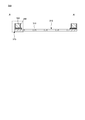
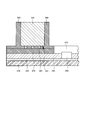
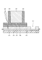
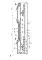
- the vapor deposition chamber 100 has a configuration capable of accommodating an object on which a vapor deposition film is formed.
- the vapor deposition source 112 is disposed below the vapor deposition substrate 104.
- the vapor deposition source 112 has a substantially rectangular shape, and is arranged along one side of the vapor deposition substrate 104.
- Such an evaporation source 112 is called a linear source type.
- the vapor deposition chamber 100 has a structure in which the vapor deposition substrate 104 and the vapor deposition source 112 move relative to each other.
- FIG. 1 shows an example in which the vapor deposition source 112 is fixed and the vapor deposition target substrate 104 moves on it.
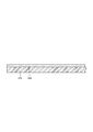
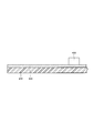
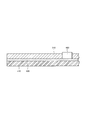
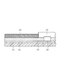
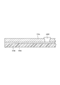
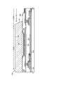
- the present invention is not limited to this, and for example, when the peeling layer 430 is not formed, a plating layer is formed on the substrate 410 exposed from the first insulating layer 450 and on the first insulating layer 450 by an electroless plating method,
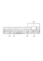
- the mask body 310 may be formed by removing (lifting off) the plating layer formed on the first insulating layer 450 by peeling off the first insulating layer 450.
- the material of the mask body 310 is not particularly limited, but a magnetic material such as nickel (Ni) or nickel alloy can be used, and Invar having a small thermal expansion is particularly preferable.
- the thickness of the mask body 310 is preferably in the range of 5 ⁇ m or more and 10 ⁇ m or less.
Landscapes
- Engineering & Computer Science (AREA)
- Manufacturing & Machinery (AREA)
- Chemical & Material Sciences (AREA)
- Chemical Kinetics & Catalysis (AREA)
- Materials Engineering (AREA)
- Mechanical Engineering (AREA)
- Metallurgy (AREA)
- Organic Chemistry (AREA)
- Electroluminescent Light Sources (AREA)
- Physical Vapour Deposition (AREA)
Priority Applications (1)
| Application Number | Priority Date | Filing Date | Title |
|---|---|---|---|
| CN201980089786.XA CN113330134B (zh) | 2019-01-31 | 2019-10-31 | 蒸镀掩模和蒸镀掩模的制造方法 |
Applications Claiming Priority (2)
| Application Number | Priority Date | Filing Date | Title |
|---|---|---|---|
| JP2019016362A JP7332301B2 (ja) | 2019-01-31 | 2019-01-31 | 蒸着マスク及び蒸着マスクの製造方法 |
| JP2019-016362 | 2019-01-31 |
Publications (1)
| Publication Number | Publication Date |
|---|---|
| WO2020158082A1 true WO2020158082A1 (ja) | 2020-08-06 |
Family
ID=71840042
Family Applications (1)
| Application Number | Title | Priority Date | Filing Date |
|---|---|---|---|
| PCT/JP2019/042845 Ceased WO2020158082A1 (ja) | 2019-01-31 | 2019-10-31 | 蒸着マスク及び蒸着マスクの製造方法 |
Country Status (3)
| Country | Link |
|---|---|
| JP (1) | JP7332301B2 (https=) |
| CN (1) | CN113330134B (https=) |
| WO (1) | WO2020158082A1 (https=) |
Cited By (2)
| Publication number | Priority date | Publication date | Assignee | Title |
|---|---|---|---|---|
| CN115537720A (zh) * | 2021-06-30 | 2022-12-30 | 株式会社日本显示器 | 蒸镀掩模 |
| WO2025187510A1 (ja) * | 2024-03-07 | 2025-09-12 | 大日本印刷株式会社 | マスク装置、マスク積層体、フレーム積層体、マスクの交換方法、及び、有機デバイスの製造方法 |
Citations (5)
| Publication number | Priority date | Publication date | Assignee | Title |
|---|---|---|---|---|
| JP2000196243A (ja) * | 1998-12-28 | 2000-07-14 | Fujitsu Ltd | フレキシブル多層回路基板の製造方法 |
| JP2003107723A (ja) * | 2001-09-25 | 2003-04-09 | Eastman Kodak Co | メタルマスクの製造方法およびメタルマスク |
| JP2004349086A (ja) * | 2003-05-21 | 2004-12-09 | Kyushu Hitachi Maxell Ltd | 有機el素子用の蒸着マスクとその製造方法 |
| JP2012114431A (ja) * | 2010-11-23 | 2012-06-14 | Ibiden Co Ltd | 半導体搭載用基板、半導体装置及び半導体装置の製造方法 |
| JP2015168848A (ja) * | 2014-03-06 | 2015-09-28 | 大日本印刷株式会社 | 基板付蒸着マスク装置の製造方法、基板付蒸着マスクおよびレジストパターン付基板 |
Family Cites Families (1)
| Publication number | Priority date | Publication date | Assignee | Title |
|---|---|---|---|---|
| US11233199B2 (en) * | 2016-02-10 | 2022-01-25 | Hon Hai Precision Industry Co., Ltd. | Vapor deposition mask manufacturing method, vapor deposition mask, and organic semiconductor element manufacturing method |
-
2019
- 2019-01-31 JP JP2019016362A patent/JP7332301B2/ja active Active
- 2019-10-31 WO PCT/JP2019/042845 patent/WO2020158082A1/ja not_active Ceased
- 2019-10-31 CN CN201980089786.XA patent/CN113330134B/zh active Active
Patent Citations (5)
| Publication number | Priority date | Publication date | Assignee | Title |
|---|---|---|---|---|
| JP2000196243A (ja) * | 1998-12-28 | 2000-07-14 | Fujitsu Ltd | フレキシブル多層回路基板の製造方法 |
| JP2003107723A (ja) * | 2001-09-25 | 2003-04-09 | Eastman Kodak Co | メタルマスクの製造方法およびメタルマスク |
| JP2004349086A (ja) * | 2003-05-21 | 2004-12-09 | Kyushu Hitachi Maxell Ltd | 有機el素子用の蒸着マスクとその製造方法 |
| JP2012114431A (ja) * | 2010-11-23 | 2012-06-14 | Ibiden Co Ltd | 半導体搭載用基板、半導体装置及び半導体装置の製造方法 |
| JP2015168848A (ja) * | 2014-03-06 | 2015-09-28 | 大日本印刷株式会社 | 基板付蒸着マスク装置の製造方法、基板付蒸着マスクおよびレジストパターン付基板 |
Non-Patent Citations (1)
| Title |
|---|
| KIMURA, KAORU: "Inorganic Adhesives", JOURNAL OF THE JAPAN WELDING SOCIETY, vol. 53, no. 2, 5 March 1984 (1984-03-05), pages 86 - 93, XP055726060 * |
Cited By (3)
| Publication number | Priority date | Publication date | Assignee | Title |
|---|---|---|---|---|
| CN115537720A (zh) * | 2021-06-30 | 2022-12-30 | 株式会社日本显示器 | 蒸镀掩模 |
| CN115537720B (zh) * | 2021-06-30 | 2024-07-19 | 株式会社日本显示器 | 蒸镀掩模 |
| WO2025187510A1 (ja) * | 2024-03-07 | 2025-09-12 | 大日本印刷株式会社 | マスク装置、マスク積層体、フレーム積層体、マスクの交換方法、及び、有機デバイスの製造方法 |
Also Published As
| Publication number | Publication date |
|---|---|
| JP2020122208A (ja) | 2020-08-13 |
| JP7332301B2 (ja) | 2023-08-23 |
| CN113330134B (zh) | 2024-01-09 |
| CN113330134A (zh) | 2021-08-31 |
Similar Documents
| Publication | Publication Date | Title |
|---|---|---|
| KR102803541B1 (ko) | 증착용 마스크 어셈블리 및 이를 사용하여 제조된 유기 발광 표시 장치 | |
| JP5003826B2 (ja) | ドナー基板、パターニング方法およびデバイスの製造方法 | |
| KR102661771B1 (ko) | 증착 마스크 및 증착 마스크의 제조 방법 | |
| US20190157561A1 (en) | Vapor deposition mask and manufacturing method of vapor deposition mask | |
| KR102475594B1 (ko) | 증착 마스크 및 그 제조 방법 | |
| KR102443587B1 (ko) | 증착 마스크 및 증착 마스크의 제조 방법 | |
| CN106256925A (zh) | 真空蒸镀装置、蒸镀膜的制造方法和有机电子器件的制造方法 | |
| JP7332301B2 (ja) | 蒸着マスク及び蒸着マスクの製造方法 | |
| JP7149196B2 (ja) | 蒸着マスク | |
| KR102723174B1 (ko) | 증착 마스크 유닛과 그 제조 방법 | |
| WO2017132908A1 (en) | A shadow mask with tapered openings formed by double electroforming using positive/negative photoresists | |
| WO2019049453A1 (ja) | 蒸着マスク、蒸着マスクの作製方法、および表示装置の製造方法 | |
| US20210214834A1 (en) | Shadow mask with tapered openings formed by double electroforming with reduced internal stresses | |
| WO2012133203A1 (ja) | 蒸着膜パターンの形成方法および有機エレクトロルミネッセンス表示装置の製造方法 | |
| WO2021044718A1 (ja) | 蒸着マスク |
Legal Events
| Date | Code | Title | Description |
|---|---|---|---|
| 121 | Ep: the epo has been informed by wipo that ep was designated in this application |
Ref document number: 19912257 Country of ref document: EP Kind code of ref document: A1 |
|
| NENP | Non-entry into the national phase |
Ref country code: DE |
|
| 122 | Ep: pct application non-entry in european phase |
Ref document number: 19912257 Country of ref document: EP Kind code of ref document: A1 |