WO2020149000A1 - 表示装置 - Google Patents
表示装置 Download PDFInfo
- Publication number
- WO2020149000A1 WO2020149000A1 PCT/JP2019/045324 JP2019045324W WO2020149000A1 WO 2020149000 A1 WO2020149000 A1 WO 2020149000A1 JP 2019045324 W JP2019045324 W JP 2019045324W WO 2020149000 A1 WO2020149000 A1 WO 2020149000A1
- Authority
- WO
- WIPO (PCT)
- Prior art keywords
- potential
- source
- period
- drain
- liquid crystal
- Prior art date
- Legal status (The legal status is an assumption and is not a legal conclusion. Google has not performed a legal analysis and makes no representation as to the accuracy of the status listed.)
- Ceased
Links
Images







Classifications
-
- G—PHYSICS
- G09—EDUCATION; CRYPTOGRAPHY; DISPLAY; ADVERTISING; SEALS
- G09G—ARRANGEMENTS OR CIRCUITS FOR CONTROL OF INDICATING DEVICES USING STATIC MEANS TO PRESENT VARIABLE INFORMATION
- G09G3/00—Control arrangements or circuits, of interest only in connection with visual indicators other than cathode-ray tubes
- G09G3/20—Control arrangements or circuits, of interest only in connection with visual indicators other than cathode-ray tubes for presentation of an assembly of a number of characters, e.g. a page, by composing the assembly by combination of individual elements arranged in a matrix no fixed position being assigned to or needed to be assigned to the individual characters or partial characters
- G09G3/34—Control arrangements or circuits, of interest only in connection with visual indicators other than cathode-ray tubes for presentation of an assembly of a number of characters, e.g. a page, by composing the assembly by combination of individual elements arranged in a matrix no fixed position being assigned to or needed to be assigned to the individual characters or partial characters by control of light from an independent source
- G09G3/3406—Control of illumination source
- G09G3/3413—Details of control of colour illumination sources
-
- G—PHYSICS
- G09—EDUCATION; CRYPTOGRAPHY; DISPLAY; ADVERTISING; SEALS
- G09G—ARRANGEMENTS OR CIRCUITS FOR CONTROL OF INDICATING DEVICES USING STATIC MEANS TO PRESENT VARIABLE INFORMATION
- G09G3/00—Control arrangements or circuits, of interest only in connection with visual indicators other than cathode-ray tubes
- G09G3/20—Control arrangements or circuits, of interest only in connection with visual indicators other than cathode-ray tubes for presentation of an assembly of a number of characters, e.g. a page, by composing the assembly by combination of individual elements arranged in a matrix no fixed position being assigned to or needed to be assigned to the individual characters or partial characters
- G09G3/34—Control arrangements or circuits, of interest only in connection with visual indicators other than cathode-ray tubes for presentation of an assembly of a number of characters, e.g. a page, by composing the assembly by combination of individual elements arranged in a matrix no fixed position being assigned to or needed to be assigned to the individual characters or partial characters by control of light from an independent source
- G09G3/36—Control arrangements or circuits, of interest only in connection with visual indicators other than cathode-ray tubes for presentation of an assembly of a number of characters, e.g. a page, by composing the assembly by combination of individual elements arranged in a matrix no fixed position being assigned to or needed to be assigned to the individual characters or partial characters by control of light from an independent source using liquid crystals
- G09G3/3611—Control of matrices with row and column drivers
- G09G3/3674—Details of drivers for scan electrodes
- G09G3/3677—Details of drivers for scan electrodes suitable for active matrices only
-
- G—PHYSICS
- G02—OPTICS
- G02F—OPTICAL DEVICES OR ARRANGEMENTS FOR THE CONTROL OF LIGHT BY MODIFICATION OF THE OPTICAL PROPERTIES OF THE MEDIA OF THE ELEMENTS INVOLVED THEREIN; NON-LINEAR OPTICS; FREQUENCY-CHANGING OF LIGHT; OPTICAL LOGIC ELEMENTS; OPTICAL ANALOGUE/DIGITAL CONVERTERS
- G02F1/00—Devices or arrangements for the control of the intensity, colour, phase, polarisation or direction of light arriving from an independent light source, e.g. switching, gating or modulating; Non-linear optics
- G02F1/01—Devices or arrangements for the control of the intensity, colour, phase, polarisation or direction of light arriving from an independent light source, e.g. switching, gating or modulating; Non-linear optics for the control of the intensity, phase, polarisation or colour
- G02F1/13—Devices or arrangements for the control of the intensity, colour, phase, polarisation or direction of light arriving from an independent light source, e.g. switching, gating or modulating; Non-linear optics for the control of the intensity, phase, polarisation or colour based on liquid crystals, e.g. single liquid crystal display cells
- G02F1/133—Constructional arrangements; Operation of liquid crystal cells; Circuit arrangements
-
- G—PHYSICS
- G09—EDUCATION; CRYPTOGRAPHY; DISPLAY; ADVERTISING; SEALS
- G09G—ARRANGEMENTS OR CIRCUITS FOR CONTROL OF INDICATING DEVICES USING STATIC MEANS TO PRESENT VARIABLE INFORMATION
- G09G3/00—Control arrangements or circuits, of interest only in connection with visual indicators other than cathode-ray tubes
- G09G3/20—Control arrangements or circuits, of interest only in connection with visual indicators other than cathode-ray tubes for presentation of an assembly of a number of characters, e.g. a page, by composing the assembly by combination of individual elements arranged in a matrix no fixed position being assigned to or needed to be assigned to the individual characters or partial characters
- G09G3/34—Control arrangements or circuits, of interest only in connection with visual indicators other than cathode-ray tubes for presentation of an assembly of a number of characters, e.g. a page, by composing the assembly by combination of individual elements arranged in a matrix no fixed position being assigned to or needed to be assigned to the individual characters or partial characters by control of light from an independent source
- G09G3/36—Control arrangements or circuits, of interest only in connection with visual indicators other than cathode-ray tubes for presentation of an assembly of a number of characters, e.g. a page, by composing the assembly by combination of individual elements arranged in a matrix no fixed position being assigned to or needed to be assigned to the individual characters or partial characters by control of light from an independent source using liquid crystals
- G09G3/3611—Control of matrices with row and column drivers
- G09G3/3614—Control of polarity reversal in general
-
- G—PHYSICS
- G09—EDUCATION; CRYPTOGRAPHY; DISPLAY; ADVERTISING; SEALS
- G09G—ARRANGEMENTS OR CIRCUITS FOR CONTROL OF INDICATING DEVICES USING STATIC MEANS TO PRESENT VARIABLE INFORMATION
- G09G3/00—Control arrangements or circuits, of interest only in connection with visual indicators other than cathode-ray tubes
- G09G3/20—Control arrangements or circuits, of interest only in connection with visual indicators other than cathode-ray tubes for presentation of an assembly of a number of characters, e.g. a page, by composing the assembly by combination of individual elements arranged in a matrix no fixed position being assigned to or needed to be assigned to the individual characters or partial characters
- G09G3/34—Control arrangements or circuits, of interest only in connection with visual indicators other than cathode-ray tubes for presentation of an assembly of a number of characters, e.g. a page, by composing the assembly by combination of individual elements arranged in a matrix no fixed position being assigned to or needed to be assigned to the individual characters or partial characters by control of light from an independent source
- G09G3/36—Control arrangements or circuits, of interest only in connection with visual indicators other than cathode-ray tubes for presentation of an assembly of a number of characters, e.g. a page, by composing the assembly by combination of individual elements arranged in a matrix no fixed position being assigned to or needed to be assigned to the individual characters or partial characters by control of light from an independent source using liquid crystals
- G09G3/3611—Control of matrices with row and column drivers
- G09G3/3648—Control of matrices with row and column drivers using an active matrix
-
- G—PHYSICS
- G09—EDUCATION; CRYPTOGRAPHY; DISPLAY; ADVERTISING; SEALS
- G09G—ARRANGEMENTS OR CIRCUITS FOR CONTROL OF INDICATING DEVICES USING STATIC MEANS TO PRESENT VARIABLE INFORMATION
- G09G3/00—Control arrangements or circuits, of interest only in connection with visual indicators other than cathode-ray tubes
- G09G3/20—Control arrangements or circuits, of interest only in connection with visual indicators other than cathode-ray tubes for presentation of an assembly of a number of characters, e.g. a page, by composing the assembly by combination of individual elements arranged in a matrix no fixed position being assigned to or needed to be assigned to the individual characters or partial characters
- G09G3/34—Control arrangements or circuits, of interest only in connection with visual indicators other than cathode-ray tubes for presentation of an assembly of a number of characters, e.g. a page, by composing the assembly by combination of individual elements arranged in a matrix no fixed position being assigned to or needed to be assigned to the individual characters or partial characters by control of light from an independent source
- G09G3/36—Control arrangements or circuits, of interest only in connection with visual indicators other than cathode-ray tubes for presentation of an assembly of a number of characters, e.g. a page, by composing the assembly by combination of individual elements arranged in a matrix no fixed position being assigned to or needed to be assigned to the individual characters or partial characters by control of light from an independent source using liquid crystals
- G09G3/3611—Control of matrices with row and column drivers
- G09G3/3696—Generation of voltages supplied to electrode drivers
-
- G—PHYSICS
- G09—EDUCATION; CRYPTOGRAPHY; DISPLAY; ADVERTISING; SEALS
- G09G—ARRANGEMENTS OR CIRCUITS FOR CONTROL OF INDICATING DEVICES USING STATIC MEANS TO PRESENT VARIABLE INFORMATION
- G09G2300/00—Aspects of the constitution of display devices
- G09G2300/04—Structural and physical details of display devices
- G09G2300/0421—Structural details of the set of electrodes
- G09G2300/0426—Layout of electrodes and connections
-
- G—PHYSICS
- G09—EDUCATION; CRYPTOGRAPHY; DISPLAY; ADVERTISING; SEALS
- G09G—ARRANGEMENTS OR CIRCUITS FOR CONTROL OF INDICATING DEVICES USING STATIC MEANS TO PRESENT VARIABLE INFORMATION
- G09G2310/00—Command of the display device
- G09G2310/02—Addressing, scanning or driving the display screen or processing steps related thereto
- G09G2310/0235—Field-sequential colour display
-
- G—PHYSICS
- G09—EDUCATION; CRYPTOGRAPHY; DISPLAY; ADVERTISING; SEALS
- G09G—ARRANGEMENTS OR CIRCUITS FOR CONTROL OF INDICATING DEVICES USING STATIC MEANS TO PRESENT VARIABLE INFORMATION
- G09G2310/00—Command of the display device
- G09G2310/02—Addressing, scanning or driving the display screen or processing steps related thereto
- G09G2310/0237—Switching ON and OFF the backlight within one frame
-
- G—PHYSICS
- G09—EDUCATION; CRYPTOGRAPHY; DISPLAY; ADVERTISING; SEALS
- G09G—ARRANGEMENTS OR CIRCUITS FOR CONTROL OF INDICATING DEVICES USING STATIC MEANS TO PRESENT VARIABLE INFORMATION
- G09G2310/00—Command of the display device
- G09G2310/08—Details of timing specific for flat panels, other than clock recovery
-
- G—PHYSICS
- G09—EDUCATION; CRYPTOGRAPHY; DISPLAY; ADVERTISING; SEALS
- G09G—ARRANGEMENTS OR CIRCUITS FOR CONTROL OF INDICATING DEVICES USING STATIC MEANS TO PRESENT VARIABLE INFORMATION
- G09G2320/00—Control of display operating conditions
- G09G2320/02—Improving the quality of display appearance
- G09G2320/0233—Improving the luminance or brightness uniformity across the screen
-
- G—PHYSICS
- G09—EDUCATION; CRYPTOGRAPHY; DISPLAY; ADVERTISING; SEALS
- G09G—ARRANGEMENTS OR CIRCUITS FOR CONTROL OF INDICATING DEVICES USING STATIC MEANS TO PRESENT VARIABLE INFORMATION
- G09G2320/00—Control of display operating conditions
- G09G2320/02—Improving the quality of display appearance
- G09G2320/0247—Flicker reduction other than flicker reduction circuits used for single beam cathode-ray tubes
-
- G—PHYSICS
- G09—EDUCATION; CRYPTOGRAPHY; DISPLAY; ADVERTISING; SEALS
- G09G—ARRANGEMENTS OR CIRCUITS FOR CONTROL OF INDICATING DEVICES USING STATIC MEANS TO PRESENT VARIABLE INFORMATION
- G09G2320/00—Control of display operating conditions
- G09G2320/04—Maintaining the quality of display appearance
- G09G2320/043—Preventing or counteracting the effects of ageing
-
- G—PHYSICS
- G09—EDUCATION; CRYPTOGRAPHY; DISPLAY; ADVERTISING; SEALS
- G09G—ARRANGEMENTS OR CIRCUITS FOR CONTROL OF INDICATING DEVICES USING STATIC MEANS TO PRESENT VARIABLE INFORMATION
- G09G2320/00—Control of display operating conditions
- G09G2320/06—Adjustment of display parameters
- G09G2320/0626—Adjustment of display parameters for control of overall brightness
-
- G—PHYSICS
- G09—EDUCATION; CRYPTOGRAPHY; DISPLAY; ADVERTISING; SEALS
- G09G—ARRANGEMENTS OR CIRCUITS FOR CONTROL OF INDICATING DEVICES USING STATIC MEANS TO PRESENT VARIABLE INFORMATION
- G09G2330/00—Aspects of power supply; Aspects of display protection and defect management
- G09G2330/02—Details of power systems and of start or stop of display operation
- G09G2330/025—Reduction of instantaneous peaks of current
Definitions
- the present invention relates to a display device.
- a liquid crystal display device in which pixels are controlled so that light of multiple colors is transmitted from the same pixel at different timings (for example, Patent Document 1).
- the present invention has been made in view of the above problems, and an object of the present invention is to provide a display device with higher image quality and capable of suppressing shortening of life due to direct current flowing through liquid crystal.
- a display device is provided with a liquid crystal display panel in which liquid crystal is sealed between two substrates facing each other and a potential difference which is provided in the liquid crystal display panel and controls alignment of the liquid crystal.
- Two electrodes, a switching element whose one of a source and a drain is connected to one of the two electrodes, and a potential which is connected to the gate of the switching element to open and close between the source and the drain of the switching element The scanning line, the signal line connected to the other of the source and the drain, and the relative potential level of the potential of one of the two electrodes and the potential of the other of the two electrodes are inverted in a predetermined cycle.
- a scanning circuit for applying any one of a first potential, a second potential, and a third potential to the scanning line, the first potential being a potential for opening the source-drain,
- the second potential is a potential closing the source-drain,
- the third potential is a potential closing the source-drain and lower than the second potential, and the predetermined period
- the source-drain is opened and closed a plurality of times inside the scanning circuit, and the scanning circuit is configured such that the other of the two electrodes is set to a potential relatively lower than one during the period in which the source-drain is closed.
- the potential of the scanning line is switched from the second potential to the third potential.
- FIG. 1 is a schematic circuit diagram showing the main configuration of the display device.
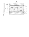
- FIG. 2 is a schematic sectional view of the liquid crystal display panel.
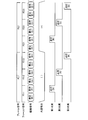
- FIG. 3 is a timing chart showing an example of the flow of field sequential control.
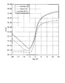
- FIG. 4 is a graph showing an example of transistor characteristics of the switching element.
- FIG. 5 is a timing chart showing a drive waveform of a row of pixels that is finally in a writing period in scanning related to pixel driving of the liquid crystal display panel according to the comparative example.
- FIG. 6 is a timing chart showing the transition of the potential applied to the pixel electrode of the pixel to which the drive waveform shown in FIG. 5 is applied.
- FIG. 7 is a timing chart showing the potential obtained by subtracting the VCOM drive signal from the potential shown in FIG. FIG.
- FIG. 8 is a timing chart showing drive waveforms of rows of pixels that are in a writing period first in scanning of the display device of the first embodiment.
- FIG. 9 is a timing chart showing the drive waveforms of the pixel rows that become the last writing period in the scan of the display device of the first embodiment.
- FIG. 10 is a timing chart showing the transition of the potential applied to the pixel electrode of the pixel to which the drive waveform shown in FIG. 8 is applied.
- FIG. 11 is a timing chart showing the transition of the potential applied to the pixel electrode of the pixel to which the drive waveform shown in FIG. 9 is applied.
- FIG. 12 is a timing chart showing the potential obtained by subtracting the VCOM drive signal from the potential shown in FIG. FIG.
- FIG. 13 is a timing chart showing the potential obtained by subtracting the VCOM drive signal from the potential shown in FIG.
- FIG. 14 is a timing chart showing drive waveforms of rows of pixels which are first in the writing period in the scanning of the second embodiment.
- FIG. 15 is a timing chart showing the drive waveforms of the pixel rows that finally become the writing period in the scanning of the second embodiment.
- FIG. 16 is a timing chart showing the transition of the potential applied to the pixel electrode of the pixel to which the drive waveform shown in FIG. 14 is applied.
- FIG. 17 is a timing chart showing the transition of the potential applied to the pixel electrode of the pixel to which the drive waveform shown in FIG. 15 is applied.
- FIG. 18 is a timing chart showing the potential obtained by subtracting the VCOM drive signal from the potential shown in FIG.
- FIG. 19 is a timing chart showing the potential obtained by subtracting the VCOM drive signal from the potential shown in FIG.
- FIG. 20 is a schematic diagram showing a configuration example of the light source device.
- FIG. 1 is a schematic circuit diagram showing the main configuration of the display device 100.
- the display device 100 includes a liquid crystal display panel P and a light source device L.
- the liquid crystal display panel P includes a display unit 7, a signal output circuit 8, a scanning circuit 9, a VCOM drive circuit 10, a timing controller 13, and a power supply circuit 14.
- a display surface one surface of the liquid crystal display panel P facing the display unit 7
- the other surface will be referred to as a back surface.
- the display unit 7 has a plurality of pixels Pix arranged in a matrix.
- the pixel Pix includes the switching element 1 and two electrodes. In FIG. 1 and FIG. 2 described later, the pixel electrode 2 and the common electrode 6 are illustrated as two electrodes.
- FIG. 2 is a schematic sectional view of the liquid crystal display panel P.
- the liquid crystal display panel P has two substrates facing each other and the liquid crystal 3 sealed between the two substrates.
- one of the two substrates will be referred to as a first substrate 30, and the other will be referred to as a second substrate 20.
- the first substrate 30 includes a translucent glass substrate 35, a pixel electrode 2 laminated on the second substrate 20 side of the glass substrate 35, and an insulation laminated on the second substrate 20 side so as to cover the pixel electrode 2. And a layer 55.
- the pixel electrode 2 is provided individually for each pixel Pix.
- the second substrate 20 includes a translucent glass substrate 21, a common electrode 6 laminated on the first substrate 30 side of the glass substrate 21, and an insulation laminated on the first substrate 30 side so as to cover the common electrode 6. And a layer 56.
- the common electrode 6 has a plate-like or film-like shape shared by the plurality of pixels Pix.
- the liquid crystal 3 of Embodiment 1 is a polymer dispersed liquid crystal. Specifically, the liquid crystal 3 includes a bulk 51 and fine particles 52. The orientation of the fine particles 52 changes according to the potential difference between the pixel electrode 2 and the common electrode 6 within the bulk 51. By controlling the electric potential of the pixel electrode 2 individually for each pixel Pix, at least either the degree of light transmission or the degree of dispersion is controlled for each pixel Pix.
- the pixel electrode 2 and the common electrode 6 face each other so as to sandwich the liquid crystal 3, but the liquid crystal display panel P has the pixel electrode 2 and the common electrode 6 on one substrate.
- the orientation of the liquid crystal 3 may be controlled by the electric field generated and provided by the pixel electrode 2 and the common electrode 6.
- the liquid crystal 3 may be a liquid crystal other than the polymer dispersed liquid crystal.
- the switching element 1 is a switching element using a semiconductor such as a thin film transistor (TFT).
- TFT thin film transistor
- One of the source and the drain of the switching element 1 is connected to one of the two electrodes (pixel electrode 2).
- the other of the source and the drain of the switching element 1 is connected to the signal line 4.
- the gate of the switching element 1 is connected to the scanning line 5.
- the scanning line 5 gives a potential for opening and closing between the source and drain of the switching element 1 under the control of the scanning circuit 9.
- the scanning circuit 9 controls the potential. Details of the potential control by the scanning circuit 9 will be described later.
- the plurality of signal lines 4 are arranged along one of the arrangement directions of the pixels Pix (row direction).
- the signal line 4 extends along the other (column direction) of the arrangement directions of the pixels Pix.
- the signal line 4 is shared by the switching elements 1 of the plurality of pixels Pix arranged in the column direction.
- the plurality of scanning lines 5 are arranged along the column direction.
- the scanning line 5 extends along the row direction.
- the scanning line 5 is shared by the switching elements 1 of the plurality of pixels Pix arranged in the row direction.
- the common electrode 6 is connected to the VCOM drive circuit 10.
- the VCOM drive circuit 10 applies a reference potential to the common electrode 6.
- the signal output circuit 8 outputs a pixel signal to the signal line 4 at a timing when the scanning circuit 9 gives a potential (first potential) that functions as a drive signal to the scanning line 5.
- the storage capacitor formed between the electrode 6 and the liquid crystal (fine particles 52) which is a capacitive load is charged.
- the voltage of the pixel Pix becomes a voltage corresponding to the pixel signal.
- the liquid crystal (fine particles 52) which is the storage capacitor and the capacitive load, holds the pixel signal.
- the orientation of the liquid crystal (fine particles 52) is controlled according to the electric field generated by the voltage of each pixel Pix and the voltage of the common electrode 6.
- a light source device L is arranged beside the liquid crystal display panel P.
- the light source device L includes a light source 11 and a light source drive circuit 12.
- the light source 11 includes a first light source 11R that emits red light, a second light source 11G that emits green light, and a third light source 11B that emits blue light.
- the first light source 11R, the second light source 11G, and the third light source 11B each emit light under the control of the light source drive circuit 12.
- the first light source 11R, the second light source 11G, and the third light source 11B of the first embodiment are light sources using light emitting elements such as light emitting diodes (LEDs: Light Emitting Diodes), but are not limited thereto.
- the light source drive circuit 12 controls the light emission timing of the first light source 11R, the second light source 11G, and the third light source 11B under the control of the timing controller 13.
- the light source device L is arranged on the side of the liquid crystal display panel P, and the light from the light source 11 is emitted from the side of the liquid crystal display panel P. It may be arranged on the back side of.
- the timing controller 13 controls the operation timing of the signal output circuit 8, the scanning circuit 9, the VCOM drive circuit 10, and the light source drive circuit 12. In the first embodiment, field sequential control is performed.
- FIG. 3 is a timing chart showing an example of the flow of field sequential control.
- FIG. 3 exemplifies a schematic timing chart of two frame periods.
- the timing chart of FIG. 3 includes information indicating frame signal output, field signal output, drive signal switching, common potential switching, and lighting timings of the first light source 11R, the second light source 11G, and the third light source 11B.
- the switching of the drive signal indicates the switching of the potential of the scanning line 5.
- Switching of the common potential indicates switching of the potential of the common electrode 6.
- the frame signal is a signal indicating the start timing of each frame period.
- a frame signal is output at the start of the period FL1 of the first frame, at the start of the period FL2 of the second frame, and at the start of the period of the next frame (third frame) following the end of the second frame. Is shown to be done.
- the field signal is a signal indicating the start timing of the field period included in each frame period.
- One frame period includes a number of field periods corresponding to the number of colors of light emitted by the light source 11.
- Each field period includes a pixel signal writing period and a pixel signal holding period by the storage capacitor.
- Writing (R+) in FIG. 3 is a writing period of the first field period FI11.
- Hold (R+) is a hold period of the first field period FI11.
- Writing (G+) is a writing period of the second field period FI12.
- Hold (G+) is a hold period of the second field period FI12.
- Writing (B+) is a writing period of the third field period FI13.
- Hold (B+) is a hold period of the third field period FI13.
- the writing (R-) is a writing period of the first field period FI21.
- Hold (R-) is a hold period of the first field period FI21.
- Writing (G-) is a writing period of the second field period FI22.
- Hold (G-) is a hold period of the second field period FI22.
- Writing (B-) is a writing period of the third field period FI23.
- Hold (B-) is a hold period of the third field period FI23.
- the writing period included in a plurality of field periods in one frame period is a period in which pixel signals corresponding to gradation values of different colors are written.
- the pixel signal corresponding to the gradation value of "r1" is written in the writing period of the first field period FI11.
- the pixel signal corresponding to the gradation value of “g1” is written in the writing period of the second field period FI12.
- the pixel signal corresponding to the gradation value of “b1” is written in the writing period of the third field period FI13.
- the holding period included in the plurality of field periods in one frame period is a period in which pixel signals corresponding to gradation values of different colors are held.
- the light sources of a plurality of colors included in the light source 11 are controlled so as to be turned on within the holding period of the corresponding field period.
- the first light source 11R is a red light source
- the second light source 11G is a green light source
- the third light source 11B is a blue light source.
- the first light source 11R is turned on during the holding period of the first field period F11.
- red scattered light corresponding to the voltage corresponding to the grayscale value (r1) of red (R) written in the writing period of the first field period F11 is emitted.
- the second light source 11G is turned on in the second field period F12.
- green scattered light corresponding to the voltage corresponding to the gradation value (g1) of green (G) written in the writing period of the second field period F12 is emitted.
- the third light source 11B is turned on in the third field period F13.
- blue scattered light corresponding to the voltage corresponding to the grayscale value (b1) of blue (B) written in the writing period of the third field period F13 is emitted.
- the writing and holding of the R, G, and B pixel signals and the illumination by the light from the corresponding color light source are included in one frame period, so that the RGB image data is converted into one frame period.
- Corresponding color reproduction takes place. The color reproduction is performed by the same mechanism in and after the period FL2 of the second frame.
- the field period frequency is the frame period frequency multiplied by the number of colors of light emitted by the light source 11.
- the frequency of the frame period is, for example, 60 Hz, but the frequency is not limited to this, and may be 120 Hz or another frequency.
- the frequency of the field period of the first embodiment is 180 Hz, but the frequency of the field period is appropriately changed according to the frequency of the frame period and the number of colors of light emitted by the light source 11. It is possible.
- the writing period and the holding period are illustrated as periods that are apparently about the same, but in reality, the holding period is longer than the writing period.
- inversion drive is performed in which the relative high and low potentials of one of the two electrodes and the other of the electrodes are inverted in a predetermined cycle.
- the VCOM drive circuit 10 is configured such that the common potential is a negative ( ⁇ ) potential in the first frame period FL1 and the common potential is a positive (+) potential in the second frame period FL2. Control the potential of 6.
- the pixel signal is written so that the potential of the pixel electrode 2 becomes positive (+) in the period FL1 of the first frame, and the potential of the pixel electrode 2 becomes negative (-) in the period FL2 of the second frame.
- the pixel signal is written so as to have the potential of (1).
- the reference numerals in parentheses in the description of the drive signals shown in FIG. 3 indicate combinations of colors and potentials of RGB gradation values corresponding to the pixel signals to be written.
- the electric potential of the pixel electrode 2 is set to correspond to the inversion driving.
- the signal output circuit 8 outputs a pixel signal for inversion driving to the signal line 4. That is, the signal output circuit 8 outputs the pixel signal such that the voltage between the pixel electrode 2 and the common electrode 6 has the same amplitude and the polarities are different according to the timing of the inversion driving of the common electrode 6.
- the VCOM drive circuit 10 switches the potential of the common electrode 6 for the inversion drive.
- the timing controller 13 synchronizes the switching timing of the potential of the pixel electrode 2 by the inversion driving circuit and the switching timing of the potential of the common electrode 6 by the VCOM driving circuit 10 in the frame period cycle.
- the potential of the pixel electrode 2 is relatively higher than the common electrode 6 in the first frame period FL1, and the potential of the pixel electrode 2 is higher than the common electrode 6 in the second frame period FL2.
- the inversion drive is performed for each frame period so as to be relatively low, this is merely a specific control example of the inversion drive method and is not limited to this.
- the potential levels of the pixel electrode 2 and the common electrode 6 may be inverted in units of a plurality of frame periods.
- the image signal (RGB data) that is the source of the pixel signal is input to the liquid crystal display panel P via the input circuit 15 included in an external image output device, for example.
- the input circuit 15 outputs a signal indicating the gradation value of each color of red (R), green (G), and blue (B) of each pixel Pix to the signal output circuit 8 based on the image signal.
- the input circuit 15 outputs to the timing controller 13 a control signal such as a synchronization signal synchronized with the signal input timing to the signal output circuit 8.
- the timing controller 13 controls the operations of the signal output circuit 8, the scanning circuit 9, the VCOM drive circuit 10, and the like based on the signal input from the input circuit 15.
- the input circuit 15 may be provided in the liquid crystal display panel P.
- the input circuit 15 may be provided as one function of a DDIC (Display Driver Integrated Circuit) designed to integrate other circuits such as the timing controller 13.
- DDIC Display Driver Integrated Circuit
- the scanning circuit 9 of the first embodiment performs scanning for shifting the driving timing of the pixels Pix in each row in units of scanning lines 5. Therefore, the timing of the writing period varies depending on the row of the pixels Pix. Further, within one field period, a writing period is set between the timing of the row of the pixels Pix which becomes the writing period first in the scanning and the timing of the row of the pixels Pix which becomes the writing period last in the scanning. The difference between the timings is the maximum.
- FIG. 4 is a graph showing an example of the thin film transistor TFT characteristics of the switching element 1.
- the vertical axis (Id[A]) in FIG. 4 indicates the magnitude of the leak current of the switching element 1.
- the horizontal axis (Vgs [V]) in FIG. 4 indicates the voltage applied between the gate and the source of the switching element 1 between the drain and the source.
- the switching element 1 is an N-type MOS transistor
- the positive direction on the horizontal axis is when the gate potential is higher than the source potential
- the negative direction on the horizontal axis is when the gate potential is lower than the source potential. is there.
- FIG. 1 is an N-type MOS transistor
- the graph in Fig. 4 shows that the leakage current increases as the distance from the origin in the lower left corner increases.
- the switching element 1 is in an ON state in which the source-drain is opened by applying a positive voltage to the gate. Further, the switching element 1 is turned off by closing the source-drain by applying a negative voltage to the gate.
- the switching element 1 has a characteristic that the leak current increases logarithmically when the negative voltage applied to the gate increases.
- the leakage current increases as the source-drain voltage of the switching element 1 increases.
- FIG. 5 is a timing chart showing a drive waveform of a row of the pixels Pix which is the last writing period in the scan related to the pixel drive of the liquid crystal display panel.
- the timing and potential of the first potential pulse 404 shown in FIG. 5 are similar to the timing and potential of the first potential pulse 1104 shown in FIG.
- FIG. 6 is a timing chart showing the transition of the potential applied to the pixel electrode 2 of the pixel Pix to which the drive waveform shown in FIG. 5 is applied.
- FIG. 6 illustrates the potential transition 601 when the gradation degree of the pixel Pix is the highest (white raster) and the potential transition 602 when the gradation degree of the pixel Pix is the lowest (black raster).
- FIG. 6 illustrates the potential transition 601 when the gradation degree of the pixel Pix is the highest (white raster) and the potential transition 602 when the gradation degree of the pixel Pix is the lowest (black raster).
- FIG. 7 is a timing chart showing the potential obtained by subtracting the VCOM drive signal 301 from the potential shown in FIG.
- the voltage transitions 801 and 802 shown in FIG. 7 are obtained by subtracting the potential transition of the VCOM drive signal 301 from the potential transitions 601 and 602. That is, it is a voltage waveform between the common electrode 6 and the pixel electrode 2.
- a period 803 corresponding to the period of the peak 603 shown in FIG. 11 is added.
- the generation period and the degree of change of the leakage current differ depending on the position of the pixel Pix in the row direction. For this reason, a phenomenon in which the degree of change in luminance varies depending on the position of the pixel Pix in the row direction and the luminance becomes uneven depending on the position of the pixel Pix in the row direction is visually recognized.
- the gate closing voltage (OFF voltage) after the first timing T1 remains at the third potential V3. Therefore, the difference between the third potential V3 and the first potential V1 of the first potential pulse 404 is larger than the difference between the second potential V2 and the first potential V1 of the first potential pulse 404, so that the voltage increase 804 is generated. Let This voltage increase 804 may cause flicker.
- the potential of the pixel electrode 2 connected to the switching element 1 is greatly shaken in the positive and negative directions by the inversion drive.
- the voltage increase 804 when the pixel electrode has a relatively low potential becomes large, and even if the potential control of the common electrode 6 facing the pixel electrode 2 is also used, the suppression of DC current and the suppression of flicker are insufficient.
- the influence of the DC current and the flicker is greater in the pixel connected to the scan line 5 in which the order in which the drive signal is applied from the scan circuit 9 is relatively later.
- FIG. 8 is a timing chart showing the drive waveforms of the rows of the pixels Pix in the first writing period in the scan of the display device 100 of the first embodiment.
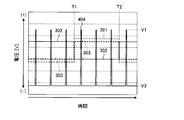
- FIG. 9 is a timing chart showing a drive waveform of the row of the pixels Pix which is the last writing period in the scan of the display device 100 of the first embodiment. 8 and 9, and FIGS. 5, 14 and 15 described later, etc., in the timing charts showing the drive waveforms, when the VCOM drive signal 301 corresponding to the waveform of the common potential and the gradation degree of the pixel Pix are the highest (white Relative pixel signal potentials 302 and relative potentials such as the pixel signal potentials 303 when the pixel Pix has the lowest gradation (black raster) are shown.
- the potential of the pixel signal potential 302 and the potential of the VCOM drive signal 301 are larger than the potential of the pixel signal potential 303.
- the potential (source voltage) that can be set in the pixel electrode 2 in the timing charts showing the drive waveforms is, for example, in the range of 0 [V] to 15 [V] in FIGS. It is within.
- the plus (+) potential of the common electrode 6 is a positive potential that is higher than 15 [V] and lower than a first potential V1 described later.
- the negative (-) potential of the common electrode 6 is a negative potential that is lower than 0 [V] and higher than a second potential V2 described later.
- the reference potential given to the common electrode 6 by the VCOM drive circuit 10 is either the plus (+) potential of the common electrode 6 or the minus ( ⁇ ) potential of the common electrode 6.
- the VCOM drive circuit 10 outputs the VCOM drive signal 301 so as to switch the potential of the common electrode 6 according to the timing of the inversion drive.
- the potential of the common electrode 6 is switched from minus ( ⁇ ) to plus (+) at the first timing T1. Further, the potential of the common electrode 6 is switched from plus (+) to minus (-) at the second timing T2.
- the timing at which the potential of the common electrode 6 is switched by the inversion driving is common regardless of the position of the pixel Pix.
- the timing of the writing period of the pixel Pix that is, the timing when the first potential V1 that opens between the source and the drain of the switching element 1 of the pixel Pix is applied to the gate of the switching element 1 is in the column direction of the pixel Pix. It depends on the position (position of pixel row).
- the application timing T3 (see FIG. 8) of the first potential V1 in the row of the pixel Pix which becomes the writing period first and the writing period last.
- the waveform of the last scanning line 5 is shown in FIG.
- the timing at which the first potential V1 is applied to the gate of the switching element 1 occurs periodically. That is, the time difference (for example, the time difference DT) caused by the position of the pixel Pix in the row direction occurs regardless of the color of the field period.
- a plurality of colors for example, red (R), green (G), and blue (B)
- the source-drain of the switching element 1 is opened and closed a plurality of times according to the gradation output. Therefore, the first potential pulse 1004 and the first potential pulse 1104 are generated a number of times corresponding to the number of colors (for example, 3) between the first timing T1 and the second timing T2 corresponding to one frame period, and the switching element is generated.
- the source-drain of 1 is opened and closed.
- the scanning circuit 9 applies the second potential V2 or the third potential V3 to the gate of the switching element 1 regardless of the position of the pixel Pix in the row direction during the period other than the timing when the first potential V1 is applied.
- the second potential V2 and the third potential V3 are potentials that close between the source and the drain.
- the third potential V3 is lower than the second potential V2.
- the scanning circuit 9 of the first embodiment applies the third potential V3 to the gate of the switching element 1 during the period when the potential of the common electrode 6 is negative ( ⁇ ). Further, the scanning circuit 9 applies the second potential V2 to the gate of the switching element 1 while the potential of the common electrode 6 is positive (+).
- the scanning circuit 9 sets the potential of the scanning line 5 to the second potential at a timing when the common electrode 6 is set to have a relatively lower potential than the pixel electrode 2 during the period in which the source and the drain are closed.
- the potential V2 is switched to the third potential V3.
- the potential of the scanning line 5 is set to the third potential V3 at the timing when the common electrode 6 is set to a potential relatively higher than that of the pixel electrode 2 within the period in which the source-drain is closed.
- the first potential V1 is, for example, 25 [V].
- the first potential V1 is set so that the switching element 1 can surely open the source-drain with respect to the maximum potential (for example, 15 [V]) given to the pixel electrode 2 of the pixel Pix.
- the second potential V2 is ⁇ 7 [V], for example.
- the third potential V3 is ⁇ 22 [V], for example.
- the second potential V2 and the third potential V3 are set with a margin so that the switching element 1 is sufficiently turned off with respect to the minimum potential (for example, 0 [V]) given to the pixel electrode 2 of the pixel Pix. To be done. That is, the third potential V3 is set with a margin such that the switching element 1 is sufficiently turned off according to the negative ( ⁇ ) potential of the common electrode 6.
- the second potential V2 is set so that the difference from the negative ( ⁇ ) potential becomes smaller.
- the plus (+) potential and the minus ( ⁇ ) potential of the common electrode 6 may be adjusted so that the DC voltage applied to the liquid crystal 3 is as small as possible in order to prolong the life of the liquid crystal 3 and suppress flicker. desirable.
- the first potential V1, the second potential V2, and the third potential V3 are generated by, for example, the power supply circuit 14 (see FIG. 1).
- the power supply circuit 14 receives supply of electric power W from the outside and supplies potentials corresponding to each of the first potential V1, the second potential V2, and the third potential V3 to the scanning circuit 9.
- the power supply circuit 14 may generate a potential suitable for the operation of each component included in the display device 100 to supply power to each component.
- the scanning circuit 9 may have a function of receiving power supply from the outside and generating the first potential V1, the second potential V2, and the third potential V3.
- FIG. 10 is a timing chart showing the transition of the potential applied to the pixel electrode 2 of the pixel Pix to which the drive waveform shown in FIG. 8 is applied.
- FIG. 10 illustrates the potential transition 1201 when the gradation degree of the pixel Pix is the highest (white raster) and the potential transition 1202 when the gradation degree of the pixel Pix is the lowest (black raster).
- FIG. 11 is a timing chart showing the transition of the potential applied to the pixel electrode 2 of the pixel Pix to which the drive waveform shown in FIG. 9 is applied.
- FIG. 10 illustrates the potential transition 1201 when the gradation degree of the pixel Pix is the highest (white raster) and the potential transition 1202 when the gradation degree of the pixel Pix is the lowest (black raster).
- FIG. 11 is a timing chart showing the transition of the potential applied to the pixel electrode 2 of the pixel Pix to which the drive waveform shown in FIG. 9 is applied.
- FIG. 11 illustrates the potential transition 1301 when the gradation degree of the pixel Pix is the highest (white raster) and the potential transition 1302 when the gradation degree of the pixel Pix is the lowest (black raster). That is, the pixel Pix connected to the first scanning line 5 when the scanning line 5 is sequentially scanned from one side (for example, the upper side in FIG. 1) to the other direction (for example, the lower side in FIG. 1).
- FIG. 11 shows the transition of the potential applied to the pixel electrode 2 of the pixel electrode 2 of the pixel Pix connected to the last scanning line 5 in FIG.
- the first potential V1 (first potential pulse 1004) is applied to the gate of the switching element 1 of the pixel Pix having the pixel electrode 2, and the signal line A pixel signal is applied from 4 to the pixel electrode 2.
- the potential applied to the pixel electrode 2 becomes a potential according to the pixel signal.
- the potential of the common electrode 6 changes due to capacitive coupling between the common electrode 6 and the pixel electrode 2 at the first timing T1. Accordingly, the pixel potential is rising (1303, 1304). Further, at the second timing T2, the pixel potential drops according to the fluctuation of the potential of the common electrode 6 due to the capacitive coupling between the common electrode 6 and the pixel electrode 2 (1305, 1306).
- the first potential V1 (first potential pulse 1104) is applied to the gate of the switching element 1 of the pixel Pix having the pixel electrode 2, and the signal line A pixel signal is applied from 4 to the pixel electrode 2.
- the potential applied to the pixel electrode 2 becomes a potential according to the pixel signal.
- the period in which the potential stays high at peaks 1303 and 1304 is longer than that at peaks 1203 and 1204.
- the period in which the potential stays low at peaks 1305 and 1306 is longer than that at peaks 1205 and 1206. This is because the timing at which the first potential V1 is applied to the gate of the switching element 1 differs depending on the position of the pixel Pix in the row direction.
- the duration of the peaks 1203, 1204, 1205, and 1206 is the shortest in the row of the pixel Pix which is the first writing period in the scan. Further, in the row of the pixel Pix which is the last writing period in the scan, the duration of the peaks 1303, 1304, 1305 and 1306 is the longest.
- the potential of the pixel electrode 2 that stays high at peaks 1303 and 1304 and the potential of the pixel electrode 2 that stays low at peaks 1305 and 1306 hardly change until the end of the peak.
- this is the period when the potential of the common electrode 6 is positive (+), the second potential V2 is applied to the gate of the switching element 1 and the potential of the common electrode 6 is negative ( ⁇ ),
- the switching element is switched by switching the potential of the common electrode 6. This is because the difference between the potential of the gate of No. 1 and the potential of the common electrode 6 is controlled so as not to be larger than necessary.
- FIG. 12 is a timing chart showing the potential obtained by subtracting the VCOM drive signal 301 from the potential shown in FIG.
- Voltage transitions 1401 and 1402 shown in FIG. 12 are obtained by subtracting the potential transition of the VCOM drive signal 301 from the potential transitions 1201 and 1202. That is, it is a voltage waveform between the common electrode 6 and the pixel electrode 2.
- a period 1403 corresponding to the period of the peak 1203 shown in FIG. 10 is added.
- FIG. 13 is a timing chart showing the potential obtained by subtracting the VCOM drive signal 301 from the potential shown in FIG.
- the voltage transitions 1501 and 1502 shown in FIG. 13 are obtained by subtracting the potential transition of the VCOM drive signal 301 from the potential transitions 1301 and 1302. That is, it is a voltage waveform between the common electrode 6 and the pixel electrode 2.
- a period 1503 corresponding to the period of the peak 1303 shown in FIG. 11 is added.
- the potentials shown in FIGS. 12 and 13 substantially indicate the voltage (holding voltage) between the pixel electrode 2 and the common electrode 6 that acts on the liquid crystal 3 of the pixel Pix.
- the holding voltage in the period 1403 shown in FIG. 12 (corresponding to 1203 in FIG. 10) is almost the same as the holding voltage before the period 1403 shown by the voltage transition 1401.
- the holding voltage in the period 1503 shown in FIG. 13 (corresponding to 1303 in FIG. 11) is almost the same as the holding voltage before the period 1503 shown by the voltage transition 1501.
- a slight voltage increase 1504 occurs at the timing corresponding to the first first potential pulse 1104 after the first timing T1, but within the range of the voltage change indicated by the voltage transition 1501. It is insignificant and does not substantially affect the translucency of the pixel Pix, that is, the brightness.
- the occurrence of flicker due to the voltage increase 1504 can be suppressed. Further, with such a slight voltage increase 1504, the generation of a direct current to the liquid crystal 3 of the pixel Pix is at a level at which there is substantially no problem, and shortening of the life of the liquid crystal 3 due to the voltage increase 1504 can be suppressed.
- the first embodiment as described above, it is possible to suppress the occurrence of the phenomenon in which the luminance becomes uneven depending on the position of the pixel Pix in the row direction. Further, according to the first embodiment, it is possible to suppress the occurrence of flicker and the shortening of the life of the liquid crystal 3. Therefore, according to the first embodiment, it is possible to suppress the shortening of the life due to the direct current flowing through the liquid crystal 3 with higher image quality.
- the timing at which the light source 11 that illuminates the liquid crystal display panel P is turned on is the holding period, that is, the potential holding period of the pixel electrode 2 set during a plurality of times when the source-drain of the switching element 1 is opened. Is. Accordingly, by illuminating the liquid crystal display panel P with light of different colors in each of a plurality of field periods within one frame period, each pixel Pix can perform output corresponding to a gradation value of a plurality of colors.
- the light source 11 also includes a first light source 11R, a second light source 11G, and a third light source 11B.
- red (R) is selected among the gradation values of red (R), green (G), and blue (B) according to RGB data. It includes a writing period of a corresponding pixel signal, a writing period of a pixel signal corresponding to green (G), and a writing period of a pixel signal corresponding to blue (B). This allows each pixel Pix to perform an output corresponding to the RGB gradation value.
- the display device according to the second embodiment is the same as the display device 100 according to the first embodiment, except for the matters noted with reference to FIGS. 14 to 19.
- FIG. 14 is a timing chart showing the drive waveforms of the rows of the pixels Pix in the writing period first in the scanning of the second embodiment.
- FIG. 15 is a timing chart showing the drive waveforms of the row of the pixels Pix which finally becomes the writing period in the scanning of the second embodiment. That is, the waveform of the first scanning line 5 when the scanning line 5 is sequentially scanned from one side (for example, the upper side of FIG. 1) to the other side (for example, the lower side of FIG. 1) in the arrangement direction is shown in FIG. The waveform of the last scanning line 5 is shown in FIG.
- the gate of the switching element 1 is connected to the first gate electrode of the switching element 1 like the scanning circuit 9 of the first embodiment. 2 potential V2 is applied. Further, the scanning circuit 9 of the second embodiment switches the potential applied to the gate of the switching element 1 from the second potential V2 to the third potential V3 at the timing when the potential of the common electrode 6 switches from plus (+) to minus ( ⁇ ). However, after the first potential pulses 1604 and 1704 generated thereafter, the potential applied to the gate of the switching element 1 is set to the second potential V2.
- the scanning circuit 9 changes the potential of the scanning line 5 to the second potential at the timing when the common electrode 6 is set to a relatively lower potential than the pixel electrode 2 during the period in which the source-drain is closed.
- the potential V2 is switched to the third potential V3.
- the potential of the scanning line 5 that was the third potential V3 before the timing of switching the source-drain between the closed state and the open state is closed after the timing.
- the second potential V2 is set when the state is set.
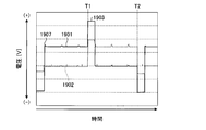
- FIG. 16 is a timing chart showing the transition of the potential applied to the pixel electrode 2 of the pixel Pix to which the drive waveform shown in FIG. 14 is applied.
- the potential transition 1801 when the gradation degree of the pixel Pix is the highest (white raster) and the potential transition 1802 when the gradation degree of the pixel Pix is the lowest (black raster) are illustrated.
- FIG. 17 is a timing chart showing the transition of the potential applied to the pixel electrode 2 of the pixel Pix to which the drive waveform shown in FIG. 15 is applied.
- the potential transition 1901 when the gradation degree of the pixel Pix is the highest (white raster) and the potential transition 1902 when the gradation degree of the pixel Pix is the lowest (black raster) are illustrated.
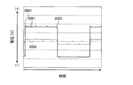
- FIG. 18 is a timing chart showing the potential obtained by subtracting the VCOM drive signal 301 from the potential shown in FIG. That is, it is a voltage waveform between the common electrode 6 and the pixel electrode 2.
- the voltage transitions 2001 and 2002 shown in FIG. 18 are obtained by subtracting the potential transition of the VCOM drive signal 301 from the potential transitions 1801 and 1802.
- a period 2003 corresponding to the period of the peak 1803 shown in FIG. 16 is added.
- FIG. 19 is a timing chart showing the potential obtained by subtracting the VCOM drive signal 301 from the potential shown in FIG.
- the voltage transitions 2101 and 2102 shown in FIG. 19 are obtained by subtracting the potential transition of the VCOM drive signal 301 from the potential transitions 1901 and 1902. That is, it is a voltage waveform between the common electrode 6 and the pixel electrode 2.
- a period 2103 corresponding to the period of the peak 1903 shown in FIG. 17 is added.
- the potential of the pixel electrode 2 is switched from the second potential V2 to the third potential V3 at the timing when the potential of the common electrode 6 is switched from plus (+) to minus ( ⁇ ), so that the common electrode before and after the timing is changed.
- the voltage between 6 and the gate of the switching element 1 is maintained at a high level to keep the source-drain closed state of the switching element 1. That is, it is possible to suppress a malfunction of the switching element 1 in which the source-drain of the switching element 1 is unintentionally opened due to the voltage between the common electrode 6 and the gate of the switching element 1 becoming low after the timing. There is.
- the potential for closing the gate is the second potential V2. That is, in the second embodiment, except for the potential difference between the gate closing potential (third potential V3) after the timing and the first potential V1 once, the gate closing potential (second potential V2) at the other timings and the gate closing potential (second potential V2) at the other timings are excluded.
- the potential difference from the one potential V1 can be made smaller. Therefore, the amount by which the holding voltage of the pixel Pix shifts to the negative voltage side can be reduced as compared with the first embodiment. Thereby, the DC balance of the liquid crystal 3 can be further improved.
- the period during which the potential of the scanning line 5 is the second potential V2 is longer than that in the first embodiment.
- the potential spike generated by the parasitic capacitance between the potential of the scanning line 5 and the source potential (the potential of the pixel electrode 2) based on the pixel signal is reduced.
- the spike 1807 in FIG. 16 the spike 1907 in FIG. 17, the spike 2007 in FIG. 18, the spike 2107 in FIG. 19, the spike 1207 in FIG. 10, the spike 1307 in FIG. 11, the spike 1407 in FIG. Is smaller than the spike 1507.
- the combination of light sources of a plurality of colors included in the light source 11 is not limited to the combination of red (R), green (G), and blue (B).
- the light source 11 may have a light source corresponding to each of the three colors of a combination of cyan, magenta, and yellow.
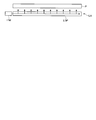
- FIG. 20 is a schematic diagram showing a configuration example of the light source device LA.
- the light source device L (or the light source device LA) only needs to be able to illuminate the liquid crystal display panel P, and its specific arrangement can be changed as appropriate.
- a plurality of colors such as a first light source 11R, a second light source 11G, and a third light source 11B are provided on the light emitting surface of the light source 11 that illuminates the liquid crystal display panel P from the back side.
- the light source may be directly arranged, or as shown in FIG. 20, the multicolor light source 11M is arranged laterally with respect to the light guide plate LGP provided on the back surface of the liquid crystal display panel P. Good.
- the multicolor light source 11M includes, for example, a light source corresponding to each of the three colors of a combination of the above-mentioned first light source 11R, second light source 11G and third light source 11B or a combination of cyan, magenta and yellow, and within one frame period. It is controlled to emit different colors of light in each field period.
- the concrete numerical values including the first electric potential V1, the second electric potential V2, the third electric potential V3, and other electric potentials illustrated above are merely examples, and the present invention is not limited to these, and two positive and negative values and a relative value. Can be appropriately changed within a range that maintains the relative relationship of.
Landscapes
- Engineering & Computer Science (AREA)
- Physics & Mathematics (AREA)
- General Physics & Mathematics (AREA)
- Theoretical Computer Science (AREA)
- Computer Hardware Design (AREA)
- Crystallography & Structural Chemistry (AREA)
- Chemical & Material Sciences (AREA)
- Nonlinear Science (AREA)
- Mathematical Physics (AREA)
- Optics & Photonics (AREA)
- Control Of Indicators Other Than Cathode Ray Tubes (AREA)
- Liquid Crystal Display Device Control (AREA)
- Liquid Crystal (AREA)
Abstract
表示装置は、対向する2枚の基板の間に液晶が封入された液晶表示パネルと、液晶表示パネルに設けられて液晶の配向を制御するための電位差が与えられる2つの電極と、ソース又はドレインの一方が2つの電極の一方と接続されるスイッチング素子と、スイッチング素子のゲートと接続されてスイッチング素子のソース-ドレイン間を開閉するための電位が与えられる走査線と、ソース又はドレインの他方と接続される信号線と、2つの電極の一方の電位と2つの電極の他方の電位との相対的な電位の高低を所定周期で反転させる反転駆動部と、走査線に第1電位、第2電位又は第3電位のいずれかを与える走査回路とを備える。
Description
本発明は、表示装置に関する。
同一画素から複数色の光をそれぞれ異なるタイミングで透過させるように画素を制御する液晶表示装置が知られている(例えば、特許文献1)。
液晶表示装置では、液晶に直流電流が流れると液晶の寿命の短縮化やフリッカの発生等の問題が生じる。このため、当該直流電流をできるだけ抑制できるよう、液晶を挟んで対向する2つの電極間の電位差を調整する方法が求められている。
本発明は、上記の課題に鑑みてなされたもので、より高画質で、液晶を流れる直流電流に起因する寿命の短縮化を抑制できる表示装置を提供することを目的とする。
本発明の一態様による表示装置は、対向する2枚の基板の間に液晶が封入された液晶表示パネルと、前記液晶表示パネルに設けられて前記液晶の配向を制御するための電位差が与えられる2つの電極と、ソース又はドレインの一方が前記2つの電極の一方と接続されるスイッチング素子と、前記スイッチング素子のゲートと接続されて前記スイッチング素子のソース-ドレイン間を開閉するための電位が与えられる走査線と、前記ソース又は前記ドレインの他方と接続される信号線と、前記2つの電極の一方の電位と前記2つの電極の他方の電位との相対的な電位の高低を所定周期で反転させる反転駆動部と、前記走査線に第1電位、第2電位又は第3電位のいずれかを与える走査回路とを備え、前記第1電位は、前記ソース-ドレイン間を開通する電位であり、前記第2電位は、前記ソース-ドレイン間を閉鎖する電位であり、前記第3電位は、前記ソース-ドレイン間を閉鎖する電位であって前記第2電位よりも低い電位であり、前記所定周期内に前記ソース-ドレイン間が複数回開閉され、前記走査回路は、前記ソース-ドレイン間を閉鎖する期間内、前記2つの電極の他方が一方よりも相対的に低電位にされるタイミングで前記走査線の電位を前記第2電位から前記第3電位に切り替える。
以下に、本発明の各実施の形態について、図面を参照しつつ説明する。なお、開示はあくまで一例にすぎず、当業者において、発明の主旨を保っての適宜変更について容易に想到し得るものについては、当然に本発明の範囲に含有されるものである。また、図面は説明をより明確にするため、実際の態様に比べ、各部の幅、厚さ、形状等について模式的に表される場合があるが、あくまで一例であって、本発明の解釈を限定するものではない。また、本明細書と各図において、既出の図に関して前述したものと同様の要素には、同一の符号を付して、詳細な説明を適宜省略することがある。
(実施形態1)
図1は、表示装置100の主要構成を示す模式的な回路図である。表示装置100は、液晶表示パネルPと、光源装置Lとを備える。液晶表示パネルPは、表示部7と、信号出力回路8と、走査回路9と、VCOM駆動回路10と、タイミングコントローラ13と、電源回路14とを備える。以下、表示部7が面する液晶表示パネルPの一面を表示面とし、他面を背面とする。
図1は、表示装置100の主要構成を示す模式的な回路図である。表示装置100は、液晶表示パネルPと、光源装置Lとを備える。液晶表示パネルPは、表示部7と、信号出力回路8と、走査回路9と、VCOM駆動回路10と、タイミングコントローラ13と、電源回路14とを備える。以下、表示部7が面する液晶表示パネルPの一面を表示面とし、他面を背面とする。
表示部7には、複数の画素Pixがマトリクス状に配置されている。画素Pixは、スイッチング素子1と、2つの電極とを含む。図1及び後述する図2では、2つの電極として、画素電極2と、共通電極6とを図示している。
図2は、液晶表示パネルPの概略断面図である。液晶表示パネルPは、対向する2枚の基板と、当該2枚の基板の間に封入された液晶3を有する。以下、当該2枚の基板の一方を第1基板30とし、他方を第2基板20とする。
第1基板30は、透光性のガラス基板35と、ガラス基板35の第2基板20側に積層された画素電極2と、画素電極2を覆うように第2基板20側に積層された絶縁層55とを含む。画素電極2は、画素Pix毎に個別に設けられる。第2基板20は、透光性のガラス基板21と、ガラス基板21の第1基板30側に積層された共通電極6と、共通電極6を覆うように第1基板30側に積層された絶縁層56とを含む。共通電極6は、複数の画素Pixで共有される板状又は膜状の形状を有する。
実施形態1の液晶3は、高分子分散型液晶である。具体的には、液晶3は、バルク51と、微粒子52とを含む。微粒子52は、バルク51内で画素電極2と共通電極6との電位差に応じて配向が変化する。画素Pix毎に画素電極2の電位が個別に制御されることで、画素Pix毎に少なくとも透光及び分散のいずれかの度合いが制御される。
図2を参照して説明した実施形態1では、画素電極2と共通電極6は、液晶3を挟むように対向するが、液晶表示パネルPは、1つの基板に画素電極2と共通電極6が設けられて画素電極2と共通電極6によって発生する電界によって液晶3の配向が制御される構成であってもよい。また、液晶3は高分子分散型液晶以外の液晶でもよい。
次に、画素電極2及び共通電極6の電位を制御する仕組みについて説明する。図1に示すようにスイッチング素子1は、例えば薄膜トランジスタ(TFT:Thin Film Transistor)等、半導体を用いたスイッチング素子である。スイッチング素子1のソース又はドレインの一方は、2つの電極の一方(画素電極2)と接続される。スイッチング素子1のソース又はドレインの他方が信号線4と接続される。スイッチング素子1のゲートは、走査線5と接続される。走査線5は、走査回路9の制御下で、スイッチング素子1のソース-ドレイン間を開閉するための電位を与える。当該電位の制御は、走査回路9が行う。走査回路9による電位の制御の詳細については後述する。
図1に示す例では、複数の信号線4は、画素Pixの並び方向のうち一方(行方向)に沿って並ぶ。信号線4は、画素Pixの並び方向のうち他方(列方向)に沿って延出する。信号線4は、列方向に並ぶ複数の画素Pixのスイッチング素子1で共有される。複数の走査線5は、列方向に沿って並ぶ。走査線5は、行方向に沿って延出する。走査線5は、行方向に並ぶ複数の画素Pixのスイッチング素子1で共有される。
共通電極6は、VCOM駆動回路10と接続される。VCOM駆動回路10は、共通電極6に基準電位を与える。走査回路9が走査線5に対して駆動信号として機能する電位(第1電位)を与えるタイミングで、信号出力回路8が信号線4に対して画素信号を出力することで、画素電極2と共通電極6との間に形成された蓄積容量と容量性負荷である液晶(微粒子52)を充電する。これによって、画素Pixの電圧は画素信号に対応した電圧となる。第1電位の印加の完了後、蓄積容量と容量性負荷である液晶(微粒子52)は画素信号を保持する。液晶(微粒子52)の配向は、各画素Pixの電圧と共通電極6の電圧によって生じる電界に応じて制御される。
図2に示すように、液晶表示パネルPの側方には、光源装置Lが配置されている。光源装置Lは、光源11と、光源駆動回路12とを備える。光源11は、赤色の光を発する第1光源11Rと、緑色の光を発する第2光源11Gと、青色の光を発する第3光源11Bと、を有する。第1光源11R、第2光源11G、第3光源11Bはそれぞれ、光源駆動回路12の制御下で発光する。実施形態1の第1光源11R、第2光源11G及び第3光源11Bは、例えば発光ダイオード(LED:Light Emitting Diode)のような発光素子を用いた光源であるが、これに限られるものでなく、発光タイミングを制御可能な光源であればよい。光源駆動回路12は、タイミングコントローラ13の制御下で第1光源11R、第2光源11G、第3光源11Bの発光タイミングを制御する。なお、図2に示す例では、光源装置Lが液晶表示パネルPの側方に配置され、光源11からの光が液晶表示パネルPの側方から照射されるが、光源11は、表示装置100の背面側に配置されていてもよい。
タイミングコントローラ13は、信号出力回路8、走査回路9、VCOM駆動回路10及び光源駆動回路12の動作タイミングを制御する。実施形態1では、フィールドシーケンシャル制御が行われる。
図3はフィールドシーケンシャル制御の流れの一例を示すタイミングチャートである。図3では2フレーム期間の概略的なタイミングチャートを例示している。図3のタイミングチャートは、フレーム信号の出力、フィールド信号の出力、駆動信号の切り替わり、共通電位の切り替わり、第1光源11R、第2光源11G及び第3光源11Bの点灯タイミングを示す情報を含む。駆動信号の切り替わりは、走査線5の電位の切り替わりを示す。共通電位の切り替わりは、共通電極6の電位の切り替わりを示す。
フレーム信号は、各フレーム期間の開始タイミングを示す信号である。図3では、1フレーム目の期間FL1の開始時と、2フレーム目の期間FL2の開始時、2フレーム目が終了した後に続く次のフレーム(3フレーム目)の期間の開始時にフレーム信号が出力されることを示している。
フィールド信号は、各フレーム期間に含まれるフィールド期間の開始タイミングを示す信号である。1フレーム期間は、光源11が発する光の色数に対応する数のフィールド期間を含む。図3では、1フレーム目の期間FL1に含まれる第1フィールド期間FI11、第2フィールド期間FI12及び第3フィールド期間FI13、2フレーム目の期間FL2に含まれる第1フィールド期間FI21、第2フィールド期間FI22及び第3フィールド期間FI23ならびに2フレーム目が終了した後に続く次のフレーム(3フレーム目)の期間の第1フィールド期間の開始時にフィールド信号が出力されることを示している。
各フィールド期間は、画素信号の書込期間と、蓄積容量による画素信号の保持期間とを含む。図3における書込(R+)は、第1フィールド期間FI11の書込期間である。保持(R+)は、第1フィールド期間FI11の保持期間である。書込(G+)は、第2フィールド期間FI12の書込期間である。保持(G+)は、第2フィールド期間FI12の保持期間である。書込(B+)は、第3フィールド期間FI13の書込期間である。保持(B+)は、第3フィールド期間FI13の保持期間である。書込(R-)は、第1フィールド期間FI21の書込期間である。保持(R-)は、第1フィールド期間FI21の保持期間である。書込(G-)は、第2フィールド期間FI22の書込期間である。保持(G-)は、第2フィールド期間FI22の保持期間である。書込(B-)は、第3フィールド期間FI23の書込期間である。保持(B-)は、第3フィールド期間FI23の保持期間である。
1フレームの期間における複数のフィールド期間に含まれる書込期間は、それぞれ異なる色の階調値に対応する画素信号が書き込まれる期間である。例えば、1フレーム目の画素信号をRGBの階調値で表した場合に(R,G,B)=(r1,g1,b1)であるとする。この場合、第1フィールド期間FI11の書込期間に「r1」の階調値に対応する画素信号が書き込まれる。また、第2フィールド期間FI12の書込期間に「g1」の階調値に対応する画素信号が書き込まれる。また、第3フィールド期間FI13の書込期間に「b1」の階調値に対応する画素信号が書き込まれる。1フレームの期間における複数のフィールド期間に含まれる保持期間は、それぞれ異なる色の階調値に対応する画素信号が保持される期間である。
光源11が有する複数の色の光源(例えば、第1光源11R、第2光源11G及び第3光源11B)は、対応するフィールド期間の保持期間内に点灯するよう制御される。例えば、第1光源11Rは赤色の光源、第2光源11Gは緑色の光源、第3光源11Bは青色の光源とされる。例えば、1フレーム目の期間FL1において、第1光源11Rは、第1フィールド期間F11の保持期間に点灯する。これによって、第1フィールド期間F11の書込期間に書き込まれた赤(R)の階調値(r1)に対応する電圧に応じた赤色の散乱光が放出される。また、1フレーム目の期間FL1において、第2光源11Gは、第2フィールド期間F12に点灯する。これによって、第2フィールド期間F12の書込期間に書き込まれた緑(G)の階調値(g1)に対応する電圧に応じた緑色の散乱光が放出される。また、1フレーム目の期間FL1において、第3光源11Bは、第3フィールド期間F13に点灯する。これによって、第3フィールド期間F13の書込期間に書き込まれた青(B)の階調値(b1)に対応する電圧に応じた青色の散乱光が放出される。このように、1フレーム期間内にR,G,Bの画素信号の書込と保持及び対応する色の光源からの光による照明とが含まれることによって、1フレーム期間内にRGBの画像データに対応する色再現が行われる。2フレーム目の期間FL2以降についても、同様の仕組みで色再現が行われる。
フィールド期間の周波数は、フレーム期間の周波数に光源11が発する光の色数を乗じたものである。実施形態1では、フレーム期間の周波数は、例えば60Hzであるが、これに限られるものでなく、120Hzであってもよいし、他の周波数であってもよい。また、フレーム期間の周波数が60Hzである場合、実施形態1のフィールド期間の周波数は180Hzであるが、フィールド期間の周波数は、フレーム期間の周波数及び光源11が発する光の色数に応じて適宜変更可能である。
また、図3では、書込期間と保持期間が見かけ上同じ程度の期間として図示されているが、実際には、保持期間は、書込期間よりも長い期間である。
液晶を利用する液晶表示パネルPでは、2つの電極の一方の電位と他方の電位との相対的な電位の高低を所定周期で反転させる反転駆動が行われる。図3では、1フレーム目の期間FL1に共通電位がマイナス(-)の電位とされ、2フレーム目の期間FL2に共通電位がプラス(+)の電位とされるようVCOM駆動回路10が共通電極6の電位を制御する。これに対応して、1フレーム目の期間FL1に画素電極2の電位がプラス(+)の電位となるよう画素信号が書き込まれ、2フレーム目の期間FL2に画素電極2の電位がマイナス(-)の電位となるよう画素信号が書き込まれる。図3に示す駆動信号の記載における括弧内の符号は、書き込まれる画素信号に対応するRGBの階調値の色と電位との組み合わせを示している。
実施形態1では、画素Pixでは、反転駆動に対応するための画素電極2の電位が行われる。具体的には、信号出力回路8が信号線4に対して反転駆動のための画素信号を出力する。すなわち、信号出力回路8は、共通電極6が反転駆動されるタイミングに応じて、画素電極2と共通電極6との間の電圧が振幅を同じくして、極性が異なるよう画素信号を出力する。また、VCOM駆動回路10が反転駆動のための共通電極6の電位の切替を行う。そして、タイミングコントローラ13が、フレーム期間周期で、反転駆動回路による画素電極2の電位の切替タイミングとVCOM駆動回路10による共通電極6の電位の切替タイミングとを同期させる。これらが実施形態1の反転駆動部として機能する。
図3に示す例では、1フレーム目の期間FL1に画素電極2の電位が共通電極6に対して相対的に高くなり、2フレーム目の期間FL2に画素電極2の電位が共通電極6に対して相対的に低くなるようフレーム期間単位で反転駆動が行われているが、これはあくまで反転駆動方式の具体的な制御例であってこれに限られるものでない。例えば、複数フレーム期間単位で画素電極2と共通電極6の電位の高低を反転するようにしてもよい。
なお、画素信号の元になる画像信号(RGBデータ)は、例えば外部の画像出力装置が有する入力回路15を介して液晶表示パネルPに入力される。入力回路15は、画像信号に基づいて各画素Pixの赤(R)、緑(G)、青(B)の各々の色の階調値を示す信号を信号出力回路8に出力する。また、入力回路15は、信号出力回路8に対する信号入力タイミングに同期した同期信号その他の制御信号をタイミングコントローラ13に出力する。タイミングコントローラ13は、入力回路15から入力される信号に基づいて信号出力回路8、走査回路9、VCOM駆動回路10等の動作を制御する。なお、入力回路15は、液晶表示パネルPに設けられてもよい。また、入力回路15は、タイミングコントローラ13等の他の回路を統合するよう設計されたDDIC(Display Driver Integrated Circuit)の一機能として設けられてもよい。
実施形態1の走査回路9は、走査線5単位で各行の画素Pixの駆動タイミングをシフトさせる走査を行う。このため、画素Pixの行によって書込期間のタイミングが異なる。また、1つのフィールド期間内では、走査において最初に書込期間になる画素Pixの行のタイミングと、走査において最後に書込期間になる画素Pixの行のタイミングとの間で書込期間になるタイミング同士の差が最大になる。
図4は、スイッチング素子1の薄膜トランジスタTFT特性の一例を示すグラフである。図4の縦軸(Id[A])は、スイッチング素子1リーク電流の大きさを示す。図4の横軸(Vgs[V])は、スイッチング素子1のドレイン―ソース間の1のゲート―ソース間に与えられる電圧を示す。スイッチング素子1をN型MOSトランジスタとしたとき、横軸の正の方向はゲート電位がソース電位に対して高い場合であり、横軸の負の方向はゲート電位がソース電位に対して低い場合である。図4では、スイッチング素子1のソース-ドレイン間電圧(Vds)が0.1[V]の場合の一点鎖線グラフ、スイッチング素子1のソース-ドレイン間電圧が5[V]の場合の破線グラフ及びスイッチング素子1のソース-ドレイン間電圧が10[V]の場合の線グラフを例示している。
図4のグラフは、左下の原点から遠ざかるほど、リーク電流が大きいことを示している。スイッチング素子1は、ゲートに正の電圧が与えられることでソース-ドレイン間が開通するオン状態になる。また、スイッチング素子1は、ゲートに負の電圧が与えられることでソース-ドレイン間が閉鎖するオフ状態になる。ここで、スイッチング素子1は、ゲートに与えられる負の電圧が大きくなると、対数的にリーク電流が多くなるという特性を有する。また、スイッチング素子1のソース-ドレイン間の電圧が大きくなるほど、リーク電流も大きくなる特性を有する。
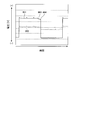
図5は、液晶表示パネルの画素駆動に係る走査において最後に書込期間になる画素Pixの行の駆動波形を示すタイミングチャートである。図5に示す第1電位パルス404のタイミング及び電位は、図9に示す第1電位パルス1104のタイミング及び電位と同様である。図6は、図5で示す駆動波形が与えられる画素Pixの画素電極2に与えられる電位の遷移を示すタイミングチャートである。図6では、画素Pixの階調度が最高である場合(白ラスター)の電位遷移601と画素Pixの階調度が最低である場合(黒ラスター)の電位遷移602とを例示している。図7は、図6に示す電位からVCOM駆動信号301を差し引いた電位を示すタイミングチャートである。図7に示す電圧遷移801,802は、電位遷移601,602からVCOM駆動信号301の電位遷移を差し引いたものである。すなわち、共通電極6と画素電極2間の電圧波形である。図13では、図11に示すピーク603の期間に対応する期間803を付している。
図5に示す例では、第1電位V1が与えられるタイミング以外の期間、第3電位V3のみが与えられている。このようなスイッチング素子1のゲート電位制御では、反転駆動後のピーク603の期間に信号線4の電位(画素電極2に与えられている電位)が走査線5の電位に比して著しく低いことに起因し、スイッチング素子1のソース-ドレイン間のリーク電流が多くなる。係るリーク電流の多さによって、ピーク603の電位変化及び期間803の電圧変化が示すように、第1タイミングT1後に第1電位パルス404がスイッチング素子1のゲートに与えられるまでの間における保持電圧の変化がより大きくなる。すなわち、画素Pixの行方向の位置によってリーク電流の発生期間及び変化の度合いに差が生じる。このため、画素Pixの行方向の位置によって輝度の変化の度合いに差が生じ、画素Pixの行方向の位置によって輝度が不均一になる現象が視認される。
また、図5に示す例では、第1タイミングT1の後のゲートの閉鎖電圧(オフ電圧)が第3電位V3のままである。このため、第3電位V3と第1電位パルス404の第1電位V1との差が第2電位V2と第1電位パルス404の第1電位V1との差よりも大きいことによって電圧上昇804を発生させる。この電圧上昇804は、フリッカを生じさせる場合がある。
このように、反転駆動によって、スイッチング素子1と接続される画素電極2の電位が正負に大きく揺さぶられる。これによって画素電極が相対的に低電位になった場合の電圧上昇804が大きくなり、画素電極2と対向する共通電極6の電位制御を併用しても直流電流の抑制及びフリッカの抑制が不十分になっていた。特に、図5を参照して説明したように、走査回路9から駆動信号が与えられる順番が相対的により後回しになる走査線5と接続されている画素では、直流電流及びフリッカの影響がより大きかった。言い換えれば、画素Pixが接続される走査線5の並び方向の位置によって、液晶表示装置の表示画面内における点灯の仕方が不均一になる現象が視認されるという問題が生じていた。これらの問題によって、液晶表示装置の画質及び寿命に問題が生じていた。
図8は、実施形態1の表示装置100の走査において最初に書込期間になる画素Pixの行の駆動波形を示すタイミングチャートである。図9は、実施形態1の表示装置100の走査において最後に書込期間になる画素Pixの行の駆動波形を示すタイミングチャートである。図8及び図9ならびに後述する図5、図14及び図15等、駆動波形を示すタイミングチャートでは、共通電位の波形に対応するVCOM駆動信号301、画素Pixの階調度が最高である場合(白ラスター)の画素信号電位302、画素Pixの階調度が最低である場合(黒ラスター)の画素信号電位303等の相対的な電位の高低を示している。なお、画素信号電位302による電位は、画素信号電位303による電位に比してVCOM駆動信号301との電位差が大きい。
なお、図8及び図9ならびに後述する図14及び図15等、駆動波形を示すタイミングチャートにおいて画素電極2に設定可能な電位(ソース電圧)は、例えば0[V]から15[V]の範囲内である。このようなソース電圧に対して、共通電極6のプラス(+)電位は、15[V]を上回り、かつ、後述する第1電位V1を下回る正の電位である。また、共通電極6のマイナス(-)電位は、0[V]を下回り、かつ、後述する第2電位V2を上回る負の電位である。VCOM駆動回路10が共通電極6に与える基準電位は、当該共通電極6のプラス(+)電位又は共通電極6のマイナス(-)電位のいずれかである。
VCOM駆動回路10は、反転駆動のタイミングに応じて共通電極6の電位を切り替えるようにVCOM駆動信号301を出力する。図8、図9等で示す例では、第1タイミングT1で共通電極6の電位がマイナス(-)からプラス(+)に切り替わっている。また、第2タイミングT2で共通電極6の電位がプラス(+)からマイナス(-)に切り替わっている。反転駆動によって共通電極6の電位が切り替わるタイミングは、画素Pixの位置に関わらず共通である。
一方、画素Pixの書込期間のタイミング、すなわち、画素Pixが有するスイッチング素子1のソース-ドレイン間を開通する第1電位V1がスイッチング素子1のゲートに与えられるタイミングは、画素Pixの列方向の位置(画素行の位置)によって異なる。同一フレーム期間の同一フィールド期間(例えば、第1フィールド期間F11)において最初に書込期間になる画素Pixの行における第1電位V1の印加タイミングT3(図8参照)と、最後に書込期間になる画素Pixの行における第1電位V1の印加タイミングT4(図8参照)との間には、時間差DTがある。すなわち、走査線5を並び方向の一方(例えば、図1の上側)から他方(例えば、図1の下方)に順に走査していくときの一番最初の走査線5の波形が図8で一番最後の走査線5の波形が図9である。
なお、図8の第1電位パルス1004及び図9の第1電位パルス1104が示すように、スイッチング素子1のゲートに第1電位V1が与えられるタイミングは周期的に生じる。すなわち、画素Pixの行方向の位置によって生じる時間差(例えば、時間差DT)は、どの色のフィールド期間であるかに関わらず生じる。
実施形態1では、図3を参照して説明したように、所定周期(例えば、1フレーム期間)内に、複数の色(例えば、赤(R)、緑(G)及び青(B))の階調出力に対応してスイッチング素子1のソース-ドレイン間が複数回開閉される。このため、1フレーム期間に対応する第1タイミングT1と第2タイミングT2の間に、第1電位パルス1004及び第1電位パルス1104が色数(例えば、3)に対応した回数発生してスイッチング素子1のソース-ドレイン間を開閉している。
走査回路9は、第1電位V1が与えられるタイミング以外の期間、画素Pixの行方向の位置に関わらず、スイッチング素子1のゲートに第2電位V2又は第3電位V3を与える。第2電位V2及び第3電位V3は、ソース-ドレイン間を閉鎖する電位である。また、第3電位V3は、第2電位V2よりも低い電位である。図8及び図9に示すように、実施形態1の走査回路9は、共通電極6の電位がマイナス(-)である期間、スイッチング素子1のゲートに第3電位V3を与える。また、走査回路9は、共通電極6の電位がプラス(+)である期間、スイッチング素子1のゲートに第2電位V2を与える。このように、実施形態1の走査回路9は、ソース-ドレイン間を閉鎖する期間内、共通電極6が画素電極2よりも相対的に低電位にされるタイミングで走査線5の電位を第2電位V2から第3電位V3に切り替える。また、実施形態1の走査回路9は、ソース-ドレイン間を閉鎖する期間内、共通電極6が画素電極2よりも相対的に高電位にされるタイミングで走査線5の電位を第3電位V3から第2電位V2に切り替える。
第1電位V1は、例えば25[V]である。第1電位V1は、画素Pixの画素電極2に与えられる最大電位(例えば、15[V])に対して、スイッチング素子1がソース-ドレイン間を確実に開放可能になるよう設定される。第2電位V2は、例えば-7[V]である。第3電位V3は、例えば-22[V]である。第2電位V2及び第3電位V3は、画素Pixの画素電極2に与えられる最小電位(例えば、0[V])に対して、スイッチング素子1が十分にオフになるようにマージンを持って設定される。すなわち、第3電位V3は、共通電極6のマイナス(-)の電位に応じてスイッチング素子1が十分にオフになるようにマージンを持って設定される。また、スイッチング素子1が十分にオフになるようにマージンを持った範囲内で、第2電位V2と共通電極6のプラス(+)の電位との差と、第3電位V3と共通電極6のマイナス(-)の電位との差がより小さくなるよう第2電位V2が設定される。
また、共通電極6のプラス(+)の電位及びマイナス(-)の電位は、液晶3の長寿命化とフリッカの抑制のため、液晶3にかかるDC電圧ができるだけ小さくなるよう調整されることが望ましい。
第1電位V1、第2電位V2及び第3電位V3は、例えば電源回路14(図1参照)によって生成される。電源回路14は、外部から電力Wの供給を受けて第1電位V1、第2電位V2及び第3電位V3の各々に対応する電位を走査回路9に供給する。図示しないが、電源回路14は、表示装置100が備える各構成の動作に適した電位を生成して各構成に電力供給を行ってもよい。走査回路9は、外部からの電力供給を受けて第1電位V1、第2電位V2及び第3電位V3を生成する機能を備えていてもよい。
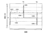
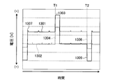
図10は、図8で示す駆動波形が与えられる画素Pixの画素電極2に与えられる電位の遷移を示すタイミングチャートである。図10では、画素Pixの階調度が最高である場合(白ラスター)の電位遷移1201と画素Pixの階調度が最低である場合(黒ラスター)の電位遷移1202とを例示している。図11は、図9で示す駆動波形が与えられる画素Pixの画素電極2に与えられる電位の遷移を示すタイミングチャートである。図11では、画素Pixの階調度が最高である場合(白ラスター)の電位遷移1301と画素Pixの階調度が最低である場合(黒ラスター)の電位遷移1302とを例示している。すなわち、走査線5を並び方向の一方(例えば、図1の上側)から他方(例えば、図1の下方)に順に走査していくときの一番最初の走査線5と接続されている画素Pixの画素電極2に与えられる電位の遷移が図10で一番最後の走査線5と接続されている画素Pixの画素電極2に与えられる電位の遷移が図11である。
図10に示す電位遷移1201,1202では、反転駆動によって共通電極6の電位がマイナス(-)からプラス(+)に切り替わる第1タイミングT1で共通電極6と画素電極2との間の容量結合により共通電極6の電位の変動に応じて画素電位が上昇している(1203,1204)。また、図10に示す電位遷移1201,1202では、反転駆動によって共通電極6の電位がプラス(+)からマイナス(-)に切り替わる第2タイミングT2で共通電極6と画素電極2との間の容量結合により共通電極6の電位の変動に応じて画素電位が降下している(1205,1206)。これらの電圧上昇(1203,1204)及び電圧降下(1205,1206)の後に画素電極2を有する画素Pixのスイッチング素子1のゲートに第1電位V1(第1電位パルス1004)が与えられ、信号線4から画素電極2に画素信号が与えられる。これによって、画素電極2に与えられる電位は、画素信号に応じた電位となる。
図11に示す電位遷移1301,1302では、図10に示す電位遷移1201,1202と同様、第1タイミングT1で共通電極6と画素電極2との間の容量結合により共通電極6の電位の変動に応じて画素電位が上昇している(1303,1304)。また、第2タイミングT2で共通電極6と画素電極2との間の容量結合により共通電極6の電位の変動に応じて画素電位が降下している(1305,1306)。これらの電圧上昇(1303,1304)及び電圧降下(1305,1306)の後に画素電極2を有する画素Pixのスイッチング素子1のゲートに第1電位V1(第1電位パルス1104)が与えられ、信号線4から画素電極2に画素信号が与えられる。これによって、画素電極2に与えられる電位は、画素信号に応じた電位となる。ここで、ピーク1303,1304で電位が高留まりする期間は、ピーク1203,1204よりも長い。また、ピーク1305,1306で電位が低留まりする期間は、ピーク1205,1206よりも長い。これは、画素Pixの行方向の位置によって、スイッチング素子1のゲートに第1電位V1が与えられるタイミングが異なるためである。従って、走査において最初に書込期間になる画素Pixの行において、ピーク1203,1204,1205,1206の継続期間が最短になる。また、走査において最後に書込期間になる画素Pixの行において、ピーク1303,1304,1305,1306の継続期間が最長になる。
実施形態1では、ピーク1303,1304で高留まりする画素電極2の電位及びピーク1305,1306で低留まりする画素電極2の電位が、ピークの終了までほとんど変化しない。これは、上述のように、共通電極6の電位がプラス(+)である期間、スイッチング素子1のゲートに第2電位V2が与えられ、共通電極6の電位がマイナス(-)である期間、スイッチング素子1のゲートに第3電位V3が与えられるようにスイッチング素子1のゲートの電位と共通電極6の電位の電位との関係が制御されることで、共通電極6の電位の切替によってスイッチング素子1のゲートの電位と共通電極6の電位の電位との差異が必要以上に大きくならないよう制御されることによる。仮に、スイッチング素子1のゲートの電位と共通電極6の電位の電位との差異が必要以上に大きくなった場合、スイッチング素子1のソース-ドレイン間のリーク電流がより多くなって画素電極2の電位を維持することが困難になるが、実施形態1では第2電位V2と第3電位V3との使い分けによってこのようなリーク電流の増加を抑制している。
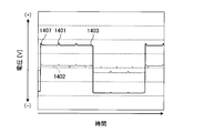
図12は、図10に示す電位からVCOM駆動信号301を差し引いた電位を示すタイミングチャートである。図12に示す電圧遷移1401,1402は、電位遷移1201,1202からVCOM駆動信号301の電位遷移を差し引いたものである。すなわち、共通電極6と画素電極2間の電圧波形である。図12では、図10に示すピーク1203の期間に対応する期間1403を付している。図13は、図11に示す電位からVCOM駆動信号301を差し引いた電位を示すタイミングチャートである。図13に示す電圧遷移1501,1502は、電位遷移1301,1302からVCOM駆動信号301の電位遷移を差し引いたものである。すなわち、共通電極6と画素電極2間の電圧波形である。図13では、図11に示すピーク1303の期間に対応する期間1503を付している。
図12及び図13に示す電位は、実質的に画素Pixの液晶3に働く画素電極2-共通電極6間の電圧(保持電圧)を示している。ここで、図12に示す期間1403(図10の1203に対応)の保持電圧は、電圧遷移1401が示す期間1403以前の保持電圧とほとんど変わらない。同様に、図13に示す期間1503(図11の1303に対応)の保持電圧は、電圧遷移1501が示す期間1503以前の保持電圧とほとんど変わらない。このように、実施形態1によれば、第1タイミングT1とその直後の第1電位V1のタイミングとの関係、すなわち、画素Pixの行方向の位置によって、保持電圧に大きな差異が生じることを抑制することができる。従って、画素Pixの行方向の位置によって輝度が不均一になる現象の発生を抑制することができる。また、図13では、第1タイミングT1の後の最初の第1電位パルス1104に対応するタイミングで電圧上昇1504がごくわずかに発生しているが、電圧遷移1501が示す電圧の変化の範囲内において微々たるものであり、画素Pixの透光性、すなわち輝度には実質的に影響しない。すなわち、電圧上昇1504によるフリッカの発生を抑制することができる。また、このようなごくわずかな電圧上昇1504では、画素Pixの液晶3に対する直流電流の発生も実質的に問題ないレベルであり、電圧上昇1504による液晶3の寿命短縮を抑制することができる。
実施形態1によれば、上述のように、画素Pixの行方向の位置によって輝度が不均一になる現象の発生を抑制することができる。また、実施形態1によれば、フリッカの発生及び液晶3の寿命短縮を抑制することができる。従って、実施形態1によれば、より高画質で、液晶3を流れる直流電流に起因する寿命の短縮化を抑制できる。
また、液晶表示パネルPを照明する光源11が点灯するタイミングは、保持期間、すなわち、スイッチング素子1のソース-ドレイン間が開通される複数回のタイミング間に設定される画素電極2の電位保持期間である。これによって、1フレーム期間内の複数のフィールド期間の各々で異なる色の光で液晶表示パネルPを照明することで、各画素Pixで複数の色の階調値に対応する出力を行える。
また、光源11は、第1光源11Rと、第2光源11Gと、第3光源11Bとを含む。また、1フレーム期間内にソース-ドレイン間が開通される複数回の開通期間は、RGBデータによる赤(R),緑(G),青(B)の階調値のうち赤(R)に対応した画素信号の書き込み期間と、緑(G)に対応した画素信号の書き込み期間と、青(B)に対応した画素信号の書き込み期間とを含む。これによって、各画素PixでRGBの階調値に対応する出力を行える。
(実施形態2)
次に、実施形態2の表示装置について、図14から図19を参照して説明する。図14から図19を参照して特筆する事項を除いて、実施形態2の表示装置は、実施形態1の表示装置100と同様である。
次に、実施形態2の表示装置について、図14から図19を参照して説明する。図14から図19を参照して特筆する事項を除いて、実施形態2の表示装置は、実施形態1の表示装置100と同様である。
図14は、実施形態2の走査において最初に書込期間になる画素Pixの行の駆動波形を示すタイミングチャートである。図15は、実施形態2の走査において最後に書込期間になる画素Pixの行の駆動波形を示すタイミングチャートである。すなわち、走査線5を並び方向の一方(例えば、図1の上側)から他方(例えば、図1の下方)に順に走査していくときの一番最初の走査線5の波形が図14で一番最後の走査線5の波形が図15である。
図14及び図15に示すように、実施形態2の走査回路9は、共通電極6の電位がプラス(+)である期間、実施形態1の走査回路9と同様、スイッチング素子1のゲートに第2電位V2を与える。また、実施形態2の走査回路9は、共通電極6の電位がプラス(+)からマイナス(-)に切り替わるタイミングでスイッチング素子1のゲートに与える電位を第2電位V2から第3電位V3に切り替えるが、その後に発生する第1電位パルス1604,1704の後、スイッチング素子1のゲートに与える電位を第2電位V2にする。このように、実施形態2の走査回路9は、ソース-ドレイン間を閉鎖する期間内、共通電極6が画素電極2よりも相対的に低電位にされるタイミングで走査線5の電位を第2電位V2から第3電位V3に切り替える。また、実施形態2の走査回路9は、ソース-ドレイン間を閉鎖状態から開通状態にするタイミングの前に第3電位V3だった走査線5の電位を、当該タイミングの後にソース-ドレイン間を閉鎖状態にする場合に第2電位V2にする。
図16は、図14で示す駆動波形が与えられる画素Pixの画素電極2に与えられる電位の遷移を示すタイミングチャートである。図16では、画素Pixの階調度が最高である場合(白ラスター)の電位遷移1801と画素Pixの階調度が最低である場合(黒ラスター)の電位遷移1802とを例示している。図17は、図15で示す駆動波形が与えられる画素Pixの画素電極2に与えられる電位の遷移を示すタイミングチャートである。図17では、画素Pixの階調度が最高である場合(白ラスター)の電位遷移1901と画素Pixの階調度が最低である場合(黒ラスター)の電位遷移1902とを例示している。
図18は、図16に示す電位からVCOM駆動信号301を差し引いた電位を示すタイミングチャートである。すなわち、共通電極6と画素電極2間の電圧波形である。図18に示す電圧遷移2001,2002は、電位遷移1801,1802からVCOM駆動信号301の電位遷移を差し引いたものである。図18では、図16に示すピーク1803の期間に対応する期間2003を付している。図19は、図17に示す電位からVCOM駆動信号301を差し引いた電位を示すタイミングチャートである。図19に示す電圧遷移2101,2102は、電位遷移1901,1902からVCOM駆動信号301の電位遷移を差し引いたものである。すなわち、共通電極6と画素電極2間の電圧波形である。図19では、図17に示すピーク1903の期間に対応する期間2103を付している。
実施形態2では、共通電極6の電位がプラス(+)からマイナス(-)に切り替わるタイミングで画素電極2の電位を第2電位V2から第3電位V3に切り替えることで、当該タイミング前後における共通電極6とスイッチング素子1のゲートとの間の電圧を高レベルで維持してスイッチング素子1のソース-ドレイン間の閉鎖状態を保持している。すなわち、当該タイミング後に共通電極6とスイッチング素子1のゲートとの間の電圧が低くなることによって意図せずスイッチング素子1のソース-ドレイン間が開放されてしまうスイッチング素子1の誤作動を抑制している。そのうえで、実施形態2では、当該タイミング後にスイッチング素子1のゲートに第1電位V1が与えられた後にはゲートを閉鎖するための電位を第2電位V2としている。すなわち、実施形態2では、当該タイミング後のゲート閉鎖電位(第3電位V3)と1回の第1電位V1との電位差を除いて、他のタイミングのゲート閉鎖電位(第2電位V2)と第1電位V1との電位差をより小さくすることができる。このため、画素Pixの保持電圧が負の電圧側にシフトする量を実施形態1よりも低減することができる。これによって、液晶3のDCバランスをより改善できる。また、実施形態2では、走査線5の電位が第2電位V2である期間が実施形態1よりも長い。これによって、走査線5の電位と画素信号に基づいたソース電位(画素電極2の電位)との間の寄生容量により発生する電位のスパイクが小さくなる。具体的には、図16のスパイク1807、図17のスパイク1907、図18のスパイク2007、図19のスパイク2107が、図10のスパイク1207、図11のスパイク1307、図12のスパイク1407、図13のスパイク1507よりも小さくなる。
なお、光源11が有する複数の色の光源の組み合わせは、赤(R)、緑(G)及び青(B)の組み合わせに限られるものでない。例えば、光源11は、シアン、マゼンタ及びイエローの組み合わせによる3色の各々に対応する光源を有していてもよい。
図20は、光源装置LAの構成例を示す模式図である。光源装置L(又は光源装置LA)は、液晶表示パネルPを照明可能であればよく、その具体的な配置については適宜変更可能である。例えば、図1で模式的に示すように、液晶表示パネルPを背面側から照明する光源11の発光面において、第1光源11R、第2光源11G、第3光源11Bのような複数の色の光源が直接配置されていてもよいし、図20に示すように、液晶表示パネルPの背面に設けられた導光板LGPに対して多色光源11Mが側方に配置された構成を採用してもよい。多色光源11Mは、例えば上述の第1光源11R、第2光源11G及び第3光源11Bの組み合わせ又はシアン、マゼンタ及びイエローの組み合わせによる3色の各々に対応する光源を含み、1フレーム期間内の各フィールド期間で異なる色の光を発するよう制御される。
また、上記で例示した第1電位V1、第2電位V2、第3電位V3その他の電位を含む具体的な数値はあくまで一例であってこれに限られるものでなく、正負及び相対する2つの値の相対的な関係を維持する範囲内で適宜変更可能である。
また、本実施形態において述べた態様によりもたらされる他の作用効果について本明細書記載から明らかなもの、又は当業者において適宜想到し得るものについては、当然に本発明によりもたらされるものと解される。
1 スイッチング素子
2 画素電極
3 液晶
4 信号線
5 走査線
52 微粒子
6 共通電極
7 表示部
8 信号出力回路
9 走査回路
10 VCOM駆動回路
11 光源
11R 第1光源
11G 第2光源
11B 第3光源
12 光源駆動回路
13 タイミングコントローラ
14 電源回路
100 表示装置
P 液晶表示パネル
L,LA 光源装置
2 画素電極
3 液晶
4 信号線
5 走査線
52 微粒子
6 共通電極
7 表示部
8 信号出力回路
9 走査回路
10 VCOM駆動回路
11 光源
11R 第1光源
11G 第2光源
11B 第3光源
12 光源駆動回路
13 タイミングコントローラ
14 電源回路
100 表示装置
P 液晶表示パネル
L,LA 光源装置
Claims (10)
- 対向する2枚の基板の間に液晶が封入された液晶表示パネルと、
前記液晶表示パネルに設けられて前記液晶の配向を制御するための電位差が与えられる2つの電極と、
ソース又はドレインの一方が前記2つの電極の一方と接続されるスイッチング素子と、
前記スイッチング素子のゲートと接続されて前記スイッチング素子のソース-ドレイン間を開閉するための電位が与えられる走査線と、
前記ソース又は前記ドレインの他方と接続される信号線と、
前記2つの電極の一方の電位と前記2つの電極の他方の電位との相対的な電位の高低を所定周期で反転させる反転駆動部と、
前記走査線に第1電位、第2電位又は第3電位のいずれかを与える走査回路とを備え、
前記第1電位は、前記ソース-ドレイン間を開通する電位であり、
前記第2電位は、前記ソース-ドレイン間を閉鎖する電位であり、
前記第3電位は、前記ソース-ドレイン間を閉鎖する電位であって前記第2電位よりも低い電位であり、
前記所定周期内に前記ソース-ドレイン間が複数回開閉され、
前記走査回路は、前記ソース-ドレイン間を閉鎖する期間内、前記2つの電極の他方が一方よりも相対的に低電位にされるタイミングで前記走査線の電位を前記第2電位から前記第3電位に切り替える
表示装置。 - 前記走査回路は、前記ソース-ドレイン間を閉鎖する期間内、前記2つの電極の他方が一方よりも相対的に高電位にされるタイミングで前記走査線の電位を前記第3電位から前記第2電位に切り替える
請求項1に記載の表示装置。 - 前記走査回路は、前記ソース-ドレイン間を閉鎖状態から開通状態にするタイミングの前に前記第3電位だった前記走査線の電位を、当該タイミングの後に前記ソース-ドレイン間を閉鎖状態にする場合に前記第2電位にする
請求項1に記載の表示装置。 - 前記液晶表示パネルを照明する光源が点灯するタイミングは、前記ソース-ドレイン間が開通される複数回のタイミング間に設定される前記2つの電極の一方の電位保持期間である
請求項1から3のいずれか一項に記載の表示装置。 - 前記光源は、第1色の光源と、第2色の光源と、第3色の光源とを含む
請求項4に記載の表示装置。 - 前記第1色、前記第2色及び前記第3色の組み合わせは、赤、緑及び青の組み合わせ又はシアン、マゼンタ及びイエローの組み合わせである
請求項5に記載の表示装置。 - 前記所定周期内に前記ソース-ドレイン間が開通される複数回の開通期間は、前記第1色に対応した画素信号の書き込み期間と、前記第2色に対応した画素信号の書き込み期間と、前記第3色に対応した画素信号の書き込み期間とを含む
請求項5又は6に記載の表示装置。 - 前記光源は、前記液晶表示パネルで画像が表示される表示面の反対側に設けられる
請求項4から7のいずれか一項に記載の表示装置。 - 前記光源は、前記液晶表示パネルの側方に設けられる
請求項4から7のいずれか一項に記載の表示装置。 - 前記液晶は、高分子分散型液晶である
請求項1から9のいずれか一項に記載の表示装置。
Priority Applications (1)
| Application Number | Priority Date | Filing Date | Title |
|---|---|---|---|
| US17/368,963 US11587522B2 (en) | 2019-01-17 | 2021-07-07 | Display device |
Applications Claiming Priority (2)
| Application Number | Priority Date | Filing Date | Title |
|---|---|---|---|
| JP2019-006365 | 2019-01-17 | ||
| JP2019006365A JP2020115179A (ja) | 2019-01-17 | 2019-01-17 | 表示装置 |
Related Child Applications (1)
| Application Number | Title | Priority Date | Filing Date |
|---|---|---|---|
| US17/368,963 Continuation US11587522B2 (en) | 2019-01-17 | 2021-07-07 | Display device |
Publications (1)
| Publication Number | Publication Date |
|---|---|
| WO2020149000A1 true WO2020149000A1 (ja) | 2020-07-23 |
Family
ID=71613770
Family Applications (1)
| Application Number | Title | Priority Date | Filing Date |
|---|---|---|---|
| PCT/JP2019/045324 Ceased WO2020149000A1 (ja) | 2019-01-17 | 2019-11-19 | 表示装置 |
Country Status (3)
| Country | Link |
|---|---|
| US (1) | US11587522B2 (ja) |
| JP (1) | JP2020115179A (ja) |
| WO (1) | WO2020149000A1 (ja) |
Families Citing this family (3)
| Publication number | Priority date | Publication date | Assignee | Title |
|---|---|---|---|---|
| JP7333701B2 (ja) * | 2019-03-08 | 2023-08-25 | 日東電工株式会社 | 高分子分散型液晶装置及び高分子分散型液晶パネルの駆動方法 |
| WO2021022540A1 (zh) * | 2019-08-08 | 2021-02-11 | 京东方科技集团股份有限公司 | 移位寄存器及其驱动方法、栅极驱动电路、显示装置 |
| JP2022012974A (ja) | 2020-07-02 | 2022-01-18 | 三菱重工業株式会社 | 廃棄物処理システム及び廃棄物処理方法 |
Citations (6)
| Publication number | Priority date | Publication date | Assignee | Title |
|---|---|---|---|---|
| JPH0277722A (ja) * | 1988-09-14 | 1990-03-16 | Hitachi Ltd | 液晶表示装置 |
| JPH0451116A (ja) * | 1990-06-19 | 1992-02-19 | Nec Corp | アクティブマトリクス液晶表示パネルの駆動方法 |
| JPH05346571A (ja) * | 1992-06-16 | 1993-12-27 | Toshiba Corp | 液晶表示装置 |
| JP2002287708A (ja) * | 2001-03-27 | 2002-10-04 | Semiconductor Energy Lab Co Ltd | 液晶表示装置及びその駆動方法 |
| JP2006171084A (ja) * | 2004-12-13 | 2006-06-29 | Nippon Hoso Kyokai <Nhk> | 液晶表示装置および液晶表示装置の駆動方法 |
| JP2018120024A (ja) * | 2017-01-23 | 2018-08-02 | 株式会社ジャパンディスプレイ | 表示装置 |
Family Cites Families (12)
| Publication number | Priority date | Publication date | Assignee | Title |
|---|---|---|---|---|
| JP2006317873A (ja) * | 2005-05-16 | 2006-11-24 | Sharp Corp | フリッカを抑制した液晶表示装置 |
| US8803787B2 (en) * | 2007-09-18 | 2014-08-12 | Japan Display Inc. | Liquid crystal display apparatus |
| KR101475298B1 (ko) * | 2007-09-21 | 2014-12-23 | 삼성디스플레이 주식회사 | 게이트 구동 회로 및 이를 구비하는 표시 장치의 구동 방법 |
| TWI383365B (zh) * | 2008-03-14 | 2013-01-21 | Chunghwa Picture Tubes Ltd | 彩色序列式顯示器之驅動方法 |
| JP5111327B2 (ja) | 2008-10-16 | 2013-01-09 | 株式会社ジャパンディスプレイウェスト | 表示撮像装置および電子機器 |
| US20120320018A1 (en) * | 2010-02-25 | 2012-12-20 | Sharp Kabushiki Kaisha | Liquid-crystal panel drive method and liquid-crystal display device |
| WO2013154039A1 (ja) * | 2012-04-13 | 2013-10-17 | シャープ株式会社 | 液晶表示装置およびその駆動方法 |
| US9214120B2 (en) * | 2012-09-12 | 2015-12-15 | Panasonic Liquid Crystal Display Co., Ltd. | Display device |
| CN103472644B (zh) * | 2013-09-25 | 2015-11-25 | 深圳市华星光电技术有限公司 | 一种阵列基板及液晶显示面板 |
| JP2018128641A (ja) * | 2017-02-10 | 2018-08-16 | 株式会社ジャパンディスプレイ | 表示装置及び調光装置 |
| US10121443B2 (en) * | 2017-02-13 | 2018-11-06 | Innolux Corporation | Display panel and display device |
| CN110675831A (zh) * | 2018-07-03 | 2020-01-10 | 夏普株式会社 | 显示装置及显示方法 |
-
2019
- 2019-01-17 JP JP2019006365A patent/JP2020115179A/ja active Pending
- 2019-11-19 WO PCT/JP2019/045324 patent/WO2020149000A1/ja not_active Ceased
-
2021
- 2021-07-07 US US17/368,963 patent/US11587522B2/en active Active
Patent Citations (6)
| Publication number | Priority date | Publication date | Assignee | Title |
|---|---|---|---|---|
| JPH0277722A (ja) * | 1988-09-14 | 1990-03-16 | Hitachi Ltd | 液晶表示装置 |
| JPH0451116A (ja) * | 1990-06-19 | 1992-02-19 | Nec Corp | アクティブマトリクス液晶表示パネルの駆動方法 |
| JPH05346571A (ja) * | 1992-06-16 | 1993-12-27 | Toshiba Corp | 液晶表示装置 |
| JP2002287708A (ja) * | 2001-03-27 | 2002-10-04 | Semiconductor Energy Lab Co Ltd | 液晶表示装置及びその駆動方法 |
| JP2006171084A (ja) * | 2004-12-13 | 2006-06-29 | Nippon Hoso Kyokai <Nhk> | 液晶表示装置および液晶表示装置の駆動方法 |
| JP2018120024A (ja) * | 2017-01-23 | 2018-08-02 | 株式会社ジャパンディスプレイ | 表示装置 |
Also Published As
| Publication number | Publication date |
|---|---|
| JP2020115179A (ja) | 2020-07-30 |
| US20210335312A1 (en) | 2021-10-28 |
| US11587522B2 (en) | 2023-02-21 |
Similar Documents
| Publication | Publication Date | Title |
|---|---|---|
| CN111833802B (zh) | 显示装置 | |
| US7233304B1 (en) | Liquid crystal display apparatus | |
| US6329971B2 (en) | Display system having electrode modulation to alter a state of an electro-optic layer | |
| KR101303538B1 (ko) | 액정표시장치와 그 구동방법 | |
| CN220105999U (zh) | 显示设备 | |
| US11587522B2 (en) | Display device | |
| US20070070024A1 (en) | Liquid crystal display device | |
| US11587519B1 (en) | Display device | |
| CN100437732C (zh) | 场序液晶显示器及其驱动方法 | |
| CN1110031C (zh) | 利用电极调制改变电光层状态的显示方法和系统 | |
| US11735132B2 (en) | Display device writes a same image to a predetermined number of lines | |
| CN101645250B (zh) | 液晶显示器 | |
| US11289032B2 (en) | Display device | |
| US9082356B2 (en) | Liquid crystal display apparatus and method of driving the same | |
| KR101869823B1 (ko) | 액정 표시장치와 이의 구동방법 | |
| KR101510885B1 (ko) | 백라이트 유닛의 광원 구동장치 및 방법 | |
| US11443702B2 (en) | Display device and display system | |
| JP2020160182A (ja) | 表示装置 | |
| JP2007512564A (ja) | 電気泳動ディスプレイにおいて輝度を改善する方法及び装置 | |
| KR102686165B1 (ko) | 표시장치 및 그 구동방법 | |
| KR20110056710A (ko) | 수평 전계형 액정표시장치 및 그 구동방법 | |
| JP4780124B2 (ja) | 液晶表示装置およびヘッドアップディスプレイ | |
| US20080284717A1 (en) | Electro-optical device, method for driving the same, and electronic machine | |
| KR100612337B1 (ko) | 박막 트랜지스터 액정 표시 장치 및 그의 구동방법 | |
| JP2006126346A (ja) | 液晶表示装置及びその駆動方法 |
Legal Events
| Date | Code | Title | Description |
|---|---|---|---|
| 121 | Ep: the epo has been informed by wipo that ep was designated in this application |
Ref document number: 19910207 Country of ref document: EP Kind code of ref document: A1 |
|
| NENP | Non-entry into the national phase |
Ref country code: DE |
|
| 122 | Ep: pct application non-entry in european phase |
Ref document number: 19910207 Country of ref document: EP Kind code of ref document: A1 |