WO2020145148A1 - 表示装置 - Google Patents
表示装置 Download PDFInfo
- Publication number
- WO2020145148A1 WO2020145148A1 PCT/JP2019/050870 JP2019050870W WO2020145148A1 WO 2020145148 A1 WO2020145148 A1 WO 2020145148A1 JP 2019050870 W JP2019050870 W JP 2019050870W WO 2020145148 A1 WO2020145148 A1 WO 2020145148A1
- Authority
- WO
- WIPO (PCT)
- Prior art keywords
- light emitting
- emitting element
- color filter
- display device
- light
- Prior art date
- Legal status (The legal status is an assumption and is not a legal conclusion. Google has not performed a legal analysis and makes no representation as to the accuracy of the status listed.)
- Ceased
Links
Images











Classifications
-
- H—ELECTRICITY
- H10—SEMICONDUCTOR DEVICES; ELECTRIC SOLID-STATE DEVICES NOT OTHERWISE PROVIDED FOR
- H10K—ORGANIC ELECTRIC SOLID-STATE DEVICES
- H10K59/00—Integrated devices, or assemblies of multiple devices, comprising at least one organic light-emitting element covered by group H10K50/00
- H10K59/30—Devices specially adapted for multicolour light emission
- H10K59/38—Devices specially adapted for multicolour light emission comprising colour filters or colour changing media [CCM]
-
- G—PHYSICS
- G02—OPTICS
- G02B—OPTICAL ELEMENTS, SYSTEMS OR APPARATUS
- G02B5/00—Optical elements other than lenses
- G02B5/20—Filters
-
- G—PHYSICS
- G02—OPTICS
- G02B—OPTICAL ELEMENTS, SYSTEMS OR APPARATUS
- G02B5/00—Optical elements other than lenses
- G02B5/20—Filters
- G02B5/201—Filters in the form of arrays
-
- G—PHYSICS
- G09—EDUCATION; CRYPTOGRAPHY; DISPLAY; ADVERTISING; SEALS
- G09F—DISPLAYING; ADVERTISING; SIGNS; LABELS OR NAME-PLATES; SEALS
- G09F9/00—Indicating arrangements for variable information in which the information is built-up on a support by selection or combination of individual elements
- G09F9/30—Indicating arrangements for variable information in which the information is built-up on a support by selection or combination of individual elements in which the desired character or characters are formed by combining individual elements
-
- G—PHYSICS
- G09—EDUCATION; CRYPTOGRAPHY; DISPLAY; ADVERTISING; SEALS
- G09F—DISPLAYING; ADVERTISING; SIGNS; LABELS OR NAME-PLATES; SEALS
- G09F9/00—Indicating arrangements for variable information in which the information is built-up on a support by selection or combination of individual elements
- G09F9/30—Indicating arrangements for variable information in which the information is built-up on a support by selection or combination of individual elements in which the desired character or characters are formed by combining individual elements
- G09F9/33—Indicating arrangements for variable information in which the information is built-up on a support by selection or combination of individual elements in which the desired character or characters are formed by combining individual elements being semiconductor devices, e.g. diodes
-
- H—ELECTRICITY
- H05—ELECTRIC TECHNIQUES NOT OTHERWISE PROVIDED FOR
- H05B—ELECTRIC HEATING; ELECTRIC LIGHT SOURCES NOT OTHERWISE PROVIDED FOR; CIRCUIT ARRANGEMENTS FOR ELECTRIC LIGHT SOURCES, IN GENERAL
- H05B33/00—Electroluminescent light sources
- H05B33/12—Light sources with substantially two-dimensional [2D] radiating surfaces
-
- H—ELECTRICITY
- H10—SEMICONDUCTOR DEVICES; ELECTRIC SOLID-STATE DEVICES NOT OTHERWISE PROVIDED FOR
- H10K—ORGANIC ELECTRIC SOLID-STATE DEVICES
- H10K59/00—Integrated devices, or assemblies of multiple devices, comprising at least one organic light-emitting element covered by group H10K50/00
- H10K59/10—OLED displays
- H10K59/12—Active-matrix OLED [AMOLED] displays
-
- H—ELECTRICITY
- H10—SEMICONDUCTOR DEVICES; ELECTRIC SOLID-STATE DEVICES NOT OTHERWISE PROVIDED FOR
- H10K—ORGANIC ELECTRIC SOLID-STATE DEVICES
- H10K59/00—Integrated devices, or assemblies of multiple devices, comprising at least one organic light-emitting element covered by group H10K50/00
- H10K59/30—Devices specially adapted for multicolour light emission
- H10K59/35—Devices specially adapted for multicolour light emission comprising red-green-blue [RGB] subpixels
-
- H—ELECTRICITY
- H10—SEMICONDUCTOR DEVICES; ELECTRIC SOLID-STATE DEVICES NOT OTHERWISE PROVIDED FOR
- H10K—ORGANIC ELECTRIC SOLID-STATE DEVICES
- H10K59/00—Integrated devices, or assemblies of multiple devices, comprising at least one organic light-emitting element covered by group H10K50/00
- H10K59/80—Constructional details
- H10K59/875—Arrangements for extracting light from the devices
Definitions
- the present disclosure relates to a display device including a plurality of light emitting elements.
- organic EL display using an organic electroluminescence (EL) element as a light emitting element
- an organic layer including at least a light emitting layer and a second electrode upper electrode, for example, on a first electrode (lower electrode, for example, anode electrode) formed separately for each pixel are formed.
- Cathode electrode is formed.
- a red light emitting element in which an organic layer that emits white light or red light and a red color filter layer are combined
- a green light emission in which an organic layer that emits white light or green light and a green color filter layer are combined.
- Each element a blue light emitting element in which an organic layer that emits white light or blue light and a blue color filter layer are combined, is provided as a sub-pixel, and one pixel is configured from these sub-pixels. Light from the light emitting layer is emitted to the outside through the second electrode (upper electrode).
- a display device that solves such a problem is known from, for example, Japanese Patent Laid-Open No. 2013-152853.
- the thickness of various layers constituting the light emitting element, the refractive index of the material constituting the various layers, the width and thickness of the color filter layer, etc. are specified. ing.
- the side surface of the color filter layer is usually in a forward taper state or a reverse taper state.
- such inclination of the side surface of the color filter layer is not taken into consideration.
- the inclination angle (taper angle) of the side surface of the color filter layer is usually different for each light emitting element, improvement in viewing angle characteristics cannot be expected unless these are taken into consideration.
- the pixel pitch is very small, the aspect ratio of the color filter layer becomes large, and the influence of the side taper state is large.
- an object of the present disclosure is to provide a display device including a plurality of light emitting elements having a configuration and a structure in which color misregistration and color mixing are unlikely to occur.
- a display device for achieving the above object is, A first light emitting element having a first light emitting region and a first color filter layer disposed above the first light emitting region; A second light emitting region, a second light emitting element including a second color filter layer disposed above the second light emitting region, and A first light emitting device including a third light emitting region and a third color filter layer disposed above the third light emitting region, A plurality of light emitting element groups each composed of are arranged on a substrate.
- the shortest line segment connecting the boundary line of the bottom surface facing the light emitting region of the color filter layer and the end of the light emitting region is formed.
- the angle ( ⁇ ) formed with the normal line of the substrate is the same in each light emitting element.
- the display device according to the second aspect of the present disclosure from the orthogonal projection image of the boundary line of the bottom face facing the light emitting region of the color filter layer to the base, The distance (L) to the orthogonal projection image with respect to the substrate is the same in each light emitting element.
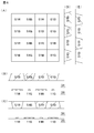
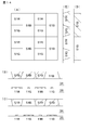
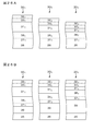
- FIG. 1 is a diagram schematically showing the arrangement of color filter layers in the display device of Example 1, and a conceptual cross-sectional view of the display device of Example 1.
- FIG. 2 is a diagram schematically showing the arrangement of color filter layers in the display device of Example 1, and a conceptual cross-sectional view of the display device of Example 1.
- FIG. 3 is a diagram schematically showing the arrangement of light emitting regions in the display device of Example 1.
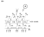
- FIG. 4 is a conceptual cross-sectional view of the display device of the first embodiment for explaining that color mixing is unlikely to occur in the display device of the first embodiment.
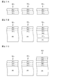
- FIG. 5 is a diagram schematically showing the arrangement of color filter layers in the display device of Example 2, and various conceptual cross-sectional views of the display device of Example 2.
- FIG. 1 is a diagram schematically showing the arrangement of color filter layers in the display device of Example 1, and a conceptual cross-sectional view of the display device of Example 1.
- FIG. 2 is a diagram schematically showing the arrangement of color filter layers in the display device of Example 1, and
- FIG. 6 is a diagram schematically showing the arrangement of color filter layers in the display device of Example 2, and various conceptual cross-sectional views of the display device of Example 2.
- FIG. 7 is a diagram schematically showing the arrangement of light emitting areas in the display device of Example 2.
- FIG. 8 is various conceptual cross-sectional views of the display device of the second embodiment for explaining that color mixing is unlikely to occur in the display device of the second embodiment.
- FIG. 9 is various conceptual cross-sectional views of the display device of the second embodiment for explaining that color mixing is unlikely to occur in the display device of the second embodiment.
- FIG. 10 is various conceptual cross-sectional views of the display device according to the second embodiment for explaining that color mixing is unlikely to occur in the display device according to the second embodiment.
- FIG. 10 is various conceptual cross-sectional views of the display device according to the second embodiment for explaining that color mixing is unlikely to occur in the display device according to the second embodiment.
- FIG. 11 is various conceptual cross-sectional views of the display device according to the second embodiment for explaining that color mixing is unlikely to occur in the display device according to the second embodiment.
- FIG. 12A, FIG. 12B, and FIG. 12C are views for explaining the mechanism in which color mixing occurs in the second embodiment and the conventional display device.
- FIG. 13 is a diagram schematically showing the arrangement of color filter layers in the display device of Example 3, and various conceptual cross-sectional views of the display device of Example 3.
- FIG. 14 is a diagram schematically showing the arrangement of color filter layers in the display device of Example 3 and various conceptual cross-sectional views of the display device of Example 3.
- FIG. 15 is a diagram schematically showing the arrangement of light emitting areas in the display device of Example 3.
- FIG. 16 is a diagram schematically showing the arrangement of color filter layers in the display device of Example 4, and various conceptual cross-sectional views of the display device of Example 3.
- 17A, 17B, 17C, 17D, 17E, 17F, and 17G are schematic partial cross-sectional views of various color filter layers.
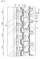
- FIG. 18 is a schematic partial cross-sectional view of the display device according to the first embodiment.
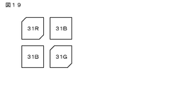
- FIG. 19 is a diagram schematically showing the arrangement of a modification of the light emitting area in the display device of the second embodiment.
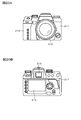
- 20A and 20B show an example in which the display device of the present disclosure is applied to a lens interchangeable single-lens reflex type digital still camera. A front view of the digital still camera is shown in FIG. 20A, and a rear view thereof is shown in FIG. 20B.
- FIG. 21 is an external view of a head mounted display showing an example in which the display device of the present disclosure is applied to the head mounted display.
- FIG. 22 is a diagram schematically showing the arrangement of color filter layers in a conventional display device, and various conceptual cross-sectional views of the conventional display device.
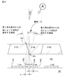
- FIG. 23 is various conceptual cross-sectional views of a conventional display device for explaining that color mixing occurs in the conventional display device.
- 24A and 24B are conceptual diagrams of the light emitting elements of the first example and the second example having a resonator structure.
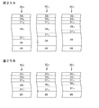
- 25A and 25B are conceptual diagrams of the light emitting elements of the third example and the fourth example having a resonator structure.
- 26A and 26B are conceptual diagrams of the light emitting elements of the fifth example and the sixth example having a resonator structure.
- 27A is a conceptual diagram of a light emitting element of a seventh example having a resonator structure
- FIGS. 27B and 27C are conceptual diagrams of a light emitting element of an eighth example having a resonator structure.
- Example 1 display device according to first to second aspects of the present disclosure
- Example 2 Modification of Example 1
- Example 3 another modification of Example 1
- Example 4 further modification of Example 1 6.
- a color filter layer surrounded by a boundary line between the color filter layer top surface (light emission surface) and the color filter layer top surface (light emission surface).
- the area (S top ) of the orthogonal projection image of the top surface region of the substrate is the same in the first light emitting element, the second light emitting element and the third light emitting element. can do.
- the first light emitting element, the second light emitting element, and the third light emitting element may have different light emitting region areas (S EL ).
- the display device is surrounded by a boundary line between the color filter layer top surface (light emission surface) and the color filter layer top surface (light emission surface).
- the area (S top ) of the orthogonal projection image of the top surface region of the color filter layer with respect to the substrate (or the first substrate or the second substrate described later) is different in the first light emitting element, the second light emitting element, and the third light emitting element.
- the first light emitting element, the second light emitting element, and the third light emitting element may have the same area (S EL ) of the light emitting region.
- the first light emitting region, the second light emitting region, and the third light emitting region emit white light.
- the first light emitting area may emit red light
- the second light emitting area may emit green light
- the third light emitting area may emit blue light.
- the fourth light emitting element that emits white light and the fourth light emitting element that emits light of a color other than red light, green light, and blue light may be added.
- the light emitting element group is composed of four light emitting elements arranged in 2 ⁇ 2, The first light emitting element is arranged adjacent to the two third light emitting elements, The second light emitting element is arranged adjacent to the two third light emitting elements, Each of the two third light-emitting elements may be arranged adjacent to the first light-emitting element and the second light-emitting element (so-called diagonal arrangement). In this case, the light emitting element group occupies a rectangular area, for example.
- the light emitting element group includes one first light emitting element, one second light emitting element, and one third light emitting element,
- the first light emitting element is arranged adjacent to the second light emitting element and the third light emitting element
- the second light emitting element may be arranged adjacent to the first light emitting element and the third light emitting element.
- the light emitting element group occupies a rectangular area, for example.
- the first light emitting element, the second light emitting element, and the third light emitting element may be arranged in a stripe array, a delta array, a rectangular array, or a pentile array.
- the shortest line segment that connects the boundary line of the bottom surface facing the light emitting region of the color filter layer and the end of the light emitting region is the base ( Alternatively, the angle ( ⁇ ) formed with the normal to the later-described first substrate or second substrate) is the same in each light emitting element.
- the base body of the boundary line of the bottom surface facing the light emitting region of the color filter layer or the first substrate or the second substrate described later.
- the distance (L) from the orthogonal projection image to the orthogonal projection image with respect to the base body (or the first substrate or the second substrate described later) at the end of the light emitting region is the same in each light emitting element.
- “same” means, for example, that the display device is divided into four regions of the first quadrant, the second quadrant, the third quadrant, and the first quadrant, and the display device is divided into five areas including the central portion and the origin of each quadrant.
- one or a plurality of light emitting element groups are appropriately selected, the angle ( ⁇ ) or the distance (L) of each light emitting element is calculated in the selected light emitting element group, and further, the angle ( ⁇ ) or the distance (L ) Average value ⁇ ave , L ave , and standard deviations ⁇ angle and ⁇ distance .
- ⁇ angle / ⁇ ave ⁇ 0.015 ⁇ distance /L ave ⁇ 0.2
- ⁇ angle / ⁇ ave >0.015 ⁇ distance /L ave >0.2 It means “different”. However, these regulations are examples.
- the display device including the preferable modes and configurations described above (hereinafter, these are collectively referred to as “display device of the present disclosure”)
- a structure made of a transparent resin (made of a transparent resin layer, for example, see JP-A-2014-089804) may be provided at the bottom including the bottom of the color filter layer in the boundary area between the adjacent color filter layers. ..
- the color filter layer is made of a resin (for example, a photocurable resin) to which a colorant composed of a desired pigment or dye is added. By selecting the pigment or dye, the target red, green, or blue color can be obtained.
- Such a color filter layer may be made of a known color resist material.
- a transparent filter may be provided in the light emitting element that emits white light.
- the display device and the like of the present disclosure are top emission type (top emission type) display devices (top emission type display devices) that emit light from the second substrate.
- a color filter layer may be formed above the first substrate, but the color filter layer may be provided on the first substrate side (OCCF structure, On-chip color filter layer structure), and may be provided on the second substrate side.
- the display device and the like of the present disclosure include a first substrate, a second substrate, and an image display unit sandwiched between the first substrate and the second substrate.
- a plurality of light emitting elements including the above-described preferred forms and configurations are arranged in a two-dimensional matrix.
- the light emitting element is formed on the first substrate side.
- the light emitting element in the display device or the like of the present disclosure is formed on the first electrode, the organic layer formed on the first electrode, the second electrode formed on the organic layer, and the second electrode. It is composed of a protective layer (planarizing layer) and a color filter layer formed on the protective layer. Then, the light from the organic layer is emitted to the outside through the second electrode, the protective layer and the color filter layer.
- the first electrode is provided for each light emitting element.
- the organic layer is provided for each light emitting element, or is provided commonly to the light emitting elements.
- the second electrode is provided commonly to the light emitting elements. That is, the second electrode is a so-called solid electrode.
- the first substrate is arranged below the base body, and the second substrate is arranged above or above the top surface of the color filter layer.
- the light emitting region is provided on the base.
- the first electrode may be in contact with part of the organic layer, or alternatively, the first electrode may be in contact with part of the organic layer. it can.
- the size of the first electrode may be smaller than that of the organic layer, or the size of the first electrode may be the same as that of the organic layer.
- the size of the first electrode may be larger than that of the organic layer, or an insulating layer may be formed between the edge of the first electrode and the organic layer. You can also A region where the first electrode and the organic layer are in contact is a light emitting region.
- the organic layer emits white light.
- the organic layer is a red light emitting layer, a green light emitting layer, and It is possible to adopt a form having a laminated structure of a blue light emitting layer.
- the organic layer may have a structure in which two layers of a blue light emitting layer that emits blue light and a yellow light emitting layer that emits yellow light are stacked, and emits white light as a whole.
- a structure in which two layers, a blue light emitting layer that emits blue light and an orange light emitting layer that emits orange light are stacked, and emits white light as a whole.
- the organic layer can be configured to include at least two light emitting layers that emit different colors.
- the light emitted from the organic layer is It can be in the form of white light.
- the organic layer includes a red light emitting layer that emits red light (wavelength: 620 nm to 750 nm), a green light emitting layer that emits green light (wavelength: 495 nm to 570 nm), and blue light (wavelength: 450 nm to 450 nm). It can have a structure in which three layers of a blue light emitting layer that emits light of 495 nm) are stacked, and emits white light as a whole.
- it may have a structure in which two layers of a blue light emitting layer that emits blue light and a yellow light emitting layer that emits yellow light are stacked, and emits white light as a whole.
- a red light emitting element is formed by combining such an organic layer that emits white light and a red color filter layer
- a green light emitting element is formed by combining an organic layer that emits white light and a green color filter layer.
- a blue light emitting element is configured by combining the organic layer that emits white light and the blue color filter layer.
- One pixel is configured by a combination of sub-pixels such as a red light emitting element, a green light emitting element and a blue light emitting element.
- one pixel may be configured by a red light emitting element, a green light emitting element, a blue light emitting element, and a light emitting element that emits white light (or a light emitting element that emits complementary color light).
- the light emitting layers that emit different colors may be mixed and not clearly separated into respective layers.
- the organic layer may have a form composed of one light emitting layer.
- the light emitting element is, for example, a red light emitting element having an organic layer containing a red light emitting layer, a green light emitting element having an organic layer containing a green light emitting layer, or a blue light emitting element having an organic layer containing a blue light emitting layer.
- a red light emitting element having an organic layer containing a red light emitting layer a green light emitting element having an organic layer containing a green light emitting layer, or a blue light emitting element having an organic layer containing a blue light emitting layer.
- a green light emitting element having an organic layer containing a green light emitting layer
- a blue light emitting element having an organic layer containing a blue light emitting layer.
- Acrylic resins, SiN, SiON, SiC, amorphous silicon ( ⁇ -Si), Al 2 O 3 , and TiO 2 can be exemplified as the material forming the protective layer (flattening layer).
- various protective methods such as various CVD methods, various coating methods, various PVD methods including a sputtering method and a vacuum evaporation method, various printing methods such as a screen printing method, and the like can be used.
- an ALD (Atomic Layer Deposition) method can also be adopted as a method for forming the protective layer.
- the protective layer may be shared by a plurality of light emitting elements, or may be provided individually in each light emitting element.
- the protective layer and the second substrate are bonded, for example, via a resin layer (sealing resin layer).
- Thermosetting adhesives such as acrylic adhesives, epoxy adhesives, urethane adhesives, silicone adhesives, and cyanoacrylate adhesives, as well as ultraviolet curable adhesives, as materials for forming the resin layer (sealing resin layer)
- An adhesive may be mentioned.
- An ultraviolet absorbing layer, a pollution preventing layer, a hard coat layer, an antistatic layer may be formed on the outermost surface of the display device that emits light (specifically, the outer surface of the second substrate).
- a cover glass may be arranged.
- an on-chip microlens may be provided on the light emitting side.
- the on-chip microlens can be made of, for example, a well-known transparent resin material such as acrylic resin, and can be obtained by melt-flowing the transparent resin material, or can be obtained by etching back. It can be obtained by a combination of a photolithography technique using a gray tone mask and an etching method, or a method of forming a transparent resin material into a lens shape based on a nanoprint method.
- the base body is formed on or above the first substrate.
- An insulating material such as SiO 2 , SiN, or SiON can be exemplified as the material forming the substrate.
- the base may be made of an insulating material having an etching selection ratio with an insulating layer or the like formed on or above the base.
- the substrate is formed by a method suitable for the material forming the substrate, specifically, various CVD methods, various coating methods, various PVD methods including sputtering methods and vacuum deposition methods, various printing methods such as screen printing methods, and plating. It can be formed by a known method such as a method, an electrodeposition method, a dipping method, a sol-gel method, or the like.
- a light emitting element drive unit is provided below or below the base body, although not limited thereto.
- the light emitting element drive unit is, for example, a transistor (specifically, for example, a MOSFET) formed on a silicon semiconductor substrate that forms the first substrate, or thin film transistors (TFT) provided on various substrates that form the first substrate. It consists of It is possible to adopt a form in which the transistor or TFT forming the light emitting element drive section and the first electrode are connected to each other through a contact hole (contact plug) formed in the base.
- the light emitting element drive section can have a known circuit configuration.
- the second electrode is connected to the light emitting element drive section through a contact hole (contact plug) formed in the base body in the outer peripheral portion of the display device.
- a light emitting element is formed on the first substrate side.
- the second electrode may be a common electrode in the plurality of light emitting elements. That is, the second electrode may be a so-called solid electrode.
- the first substrate or the second substrate may be a silicon semiconductor substrate, a high strain point glass substrate, a soda glass (Na 2 O ⁇ CaO ⁇ SiO 2 ) substrate, a borosilicate glass (Na 2 O ⁇ B 2 O 3 ⁇ SiO 2 ) substrate.
- the materials forming the first substrate and the second substrate may be the same or different. However, the second substrate is required to be transparent to the light from the light emitting element.
- the first electrode functions as an anode electrode as a material forming the first electrode
- platinum Pt
- gold Au
- silver Ag
- chromium Cr
- tungsten W
- nickel Ni
- copper Cu
- iron Fe
- cobalt Co
- tantalum Ta
- a high work function metal or alloy for example, silver as a main component, and 0.3 mass% to 1 mass% of palladium
- Examples thereof include Ag-Pd-Cu alloy containing Pd) and 0.3 mass% to 1 mass% of copper (Cu), Al-Nd alloy, and Al-Cu alloy).
- the first electrode may be 0.1 ⁇ m to 1 ⁇ m.
- a light reflection layer described later is provided, as a material forming the first electrode.
- ITO Indium Tin Oxide, Sn-doped In 2 O 3 , crystalline ITO and amorphous ITO
- the transparent conductive material include a transparent conductive material having a type oxide, an oxide having a YbFe 2 O 4 structure, a gallium oxide, a titanium oxide,
- a hole injecting property such as an oxide of indium and tin (ITO) or an oxide of indium and zinc (IZO) is formed on a dielectric multilayer film or a reflective film having high light reflectivity such as aluminum (Al). It is also possible to have a structure in which excellent transparent conductive materials are laminated.
- the first electrode when the first electrode is made to function as a cathode electrode, it is desirable that the first electrode be made of a conductive material having a small work function and a high light reflectance. It can also be used as a cathode electrode by improving the electron injection property by providing an appropriate electron injection layer.
- the second electrode functions as a cathode electrode as a material (semi-light transmissive material or light transmissive material) forming the second electrode, the emitted light is transmitted, and moreover, electrons are efficiently transmitted to the organic layer (light emitting layer). It is desirable to use a conductive material having a small work function value so that it can be implanted selectively.
- Al aluminum (Al), silver (Ag), magnesium (Mg), calcium (Ca), sodium (Na), strontium ( Sr), alkali metal or alkaline earth metal and silver (Ag)
- alloy of magnesium (Mg) and silver (Ag) (Mg-Ag alloy) alloy of magnesium-calcium (Mg-Ca alloy)
- a metal or an alloy having a small work function such as an alloy of aluminum (Al) and lithium (Li) (Al—Li alloy), and among them, a Mg—Ag alloy is preferable, and a volume ratio of magnesium to silver is used.
- Mg:Ag 5:1 to 30:1.
- the thickness of the second electrode include 4 nm to 50 nm, preferably 4 nm to 20 nm, and more preferably 6 nm to 12 nm.
- at least one material selected from the group consisting of Ag-Nd-Cu, Ag-Cu, Au and Al-Cu can be mentioned.
- the second electrode is laminated from the organic layer side with the above-mentioned material layer and a so-called transparent electrode (for example, a thickness of 3 ⁇ 10 ⁇ 8 m to 1 ⁇ 10 ⁇ 6 m) made of, for example, ITO or IZO. It can also be a structure.
- a bus electrode (auxiliary electrode) made of a low resistance material such as aluminum, aluminum alloy, silver, silver alloy, copper, copper alloy, gold or gold alloy is provided for the second electrode to reduce the resistance of the entire second electrode. May be planned.
- the average light transmittance of the second electrode is 50% to 90%, preferably 60% to 90%.
- the second electrode when the second electrode functions as an anode electrode, it is desirable that the second electrode is made of a conductive material that transmits emitted light and has a large work function value.
- an electron beam vapor deposition method for example, an electron beam vapor deposition method, a hot filament vapor deposition method, a vapor deposition method including a vacuum vapor deposition method, a sputtering method, a chemical vapor deposition method (CVD method), a MOCVD method, an ion method, etc.
- a method of forming the first electrode and the second electrode for example, an electron beam vapor deposition method, a hot filament vapor deposition method, a vapor deposition method including a vacuum vapor deposition method, a sputtering method, a chemical vapor deposition method (CVD method), a MOCVD method, an ion method, etc.
- CVD method chemical vapor deposition method
- MOCVD method a MOCVD method
- an ion method etc.
- Combination of plating method and etching method various printing methods such as screen printing method, inkjet printing method, metal mask printing method; plating method (electroplating method or electroless plat
- the first electrode and the second electrode having a desired shape (pattern).
- the second electrode may be formed based on a film forming method such as a vacuum evaporation method in which the energy of the film forming particles is small, or a MOCVD method. It is preferable from the viewpoint of preventing damage to the organic layer.
- a non-light-emitting pixel or non-light-emitting sub-pixel
- a dark spot may occur due to a leak current.
- the organic layer is provided with a light emitting layer made of an organic light emitting material.
- a light emitting layer made of an organic light emitting material.
- it has a laminated structure of a hole transport layer, a light emitting layer and an electron transport layer, and also serves as a hole transport layer and an electron transport layer It may have a laminated structure with a light emitting layer, a laminated structure with a hole injection layer, a hole transport layer, a light emitting layer, an electron transport layer and an electron injection layer, or the like.
- a physical vapor deposition method such as a vacuum deposition method
- a printing method such as a screen printing method or an inkjet printing method
- a layer of a laser absorption layer and an organic layer formed on a transfer substrate A laser transfer method in which an organic layer on a laser absorption layer is separated by irradiating a structure with a laser to transfer the organic layer, and various coating methods can be exemplified.
- a so-called metal mask is used, and the organic layer can be obtained by depositing the material that has passed through the opening provided in the metal mask.
- an insulating layer and an interlayer insulating layer are formed.
- the insulating material constituting these SiO 2 , NSG (non-doped silicate glass), BPSG (boron phosphorus silicate glass) is used. ), construction PSG, BSG, AsSG, SbSG, PbSG, SOG ( spin on glass), LTO (low Temperature oxide, low temperature CVD-SiO 2), low-melting glass, SiO X materials such as glass paste (silicon oxide film Materials); SiN-based materials including SiON-based materials; SiOC; SiOF; SiCN.
- Inorganic insulating materials such as (Nb 2 O 5 ), tin oxide (SnO 2 ) and vanadium oxide (VO x ) can be mentioned.
- Materials of 5 or less specifically, for example, fluorocarbon, cycloperfluorocarbon polymer, benzocyclobutene, cyclic fluororesin, polytetrafluoroethylene, amorphous tetrafluoroethylene, polyaryl ether, fluorinated aryl ether, fluorine Polyimide, amorphous carbon, parylene (polyparaxylylene), fullerene fluoride), Silk (trademark of The Dow Chemical Co., coating type low dielectric constant interlayer insulating film material), Flare ( It is a trademark of Honeywell Electronic Materials Co., and polyallyl ether (PAE)-based material) can also be exemplified. And these can be used individually or in appropriate combination.
- the substrate may be composed of the materials described above.
- the insulating layer, the interlayer insulating layer, and the substrate are various CVD methods, various coating methods, various PVD methods including sputtering methods and vacuum deposition methods, various printing methods such as screen printing methods, plating methods, electrodeposition methods, dipping methods, sol- It can be formed based on a known method such as a gel method.
- the display device and the like of the present disclosure including the various preferable forms and configurations described above can be configured to include an organic electroluminescence display device (organic EL display device), and the light emitting element can be an organic electroluminescence element ( It can be configured to include an organic EL element).
- organic electroluminescence display device organic EL display device
- the light emitting element can be an organic electroluminescence element ( It can be configured to include an organic EL element).
- the organic EL display device preferably has a resonator structure in order to further improve the light extraction efficiency.
- the first interface constituted by the interface between the first electrode and the organic layer (or the interlayer insulating layer is provided below the first electrode, and the light reflecting layer is provided below the interlayer insulating layer).
- the light emitting layer is provided between the first interface formed by the interface between the light reflection layer and the interlayer insulating layer) and the second interface formed by the interface between the second electrode and the organic layer. The emitted light is resonated, and a part thereof is emitted from the second electrode.
- the distance from the maximum light emitting position of the light emitting layer to the first interface is L 1
- the optical distance is OL 1
- the distance from the maximum light emitting position of the light emitting layer to the second interface is L 2
- the optical distance is OL 2
- m When 1 and m 2 are integers, the following expressions (1-1) and (1-2) are satisfied.
- ⁇ maximum peak wavelength of the spectrum of light generated in the light emitting layer (or a desired wavelength of light generated in the light emitting layer)
- ⁇ 1 Phase shift amount of light reflected at the first interface (unit: radian).
- ⁇ 2 ⁇ 1 ⁇ 0 ⁇ 2 Amount of phase shift of light reflected by the second interface (unit: radian).
- the value of m 1 is larger than or equal to zero
- the value of m 2 is independently a value of m 1, is a value of 0 or more
- (m 1, m 2) (0,0 )
- (m 1 , m 2 ) (0,1)
- (m 1 , m 2 ) (1,0)
- the distance L 1 from the maximum light emitting position of the light emitting layer to the first interface refers to the actual distance (physical distance) from the maximum light emitting position of the light emitting layer to the first interface, and is the second distance from the maximum light emitting position of the light emitting layer.
- the distance L 2 to the interface refers to an actual distance (physical distance) from the maximum light emitting position of the light emitting layer to the second interface.
- the optical distance is also called an optical path length, and generally refers to n ⁇ L when a light ray passes a distance L through a medium having a refractive index n. The same applies to the following.
- the average refractive index n ave is the sum of the products of the refractive index and the thickness of each layer forming the organic layer (or the organic layer, the first electrode, and the interlayer insulating layer), and the organic layer (or the organic layer). , The first electrode and the interlayer insulating layer).
- the first electrode or the light reflecting layer and the second electrode absorb part of the incident light and reflect the rest. Therefore, a phase shift occurs in the reflected light.
- the phase shift amounts ⁇ 1 and ⁇ 2 are obtained by measuring the values of the real part and the imaginary part of the complex refractive index of the material forming the first electrode or the light reflecting layer and the second electrode using, for example, an ellipsometer, It can be obtained by performing a calculation based on the value (see, for example, "Principles of Optic", Max Born and Emil Wolf, 1974 (PERGAMON PRESS)).
- the refractive index of the organic layer, the interlayer insulating layer, etc. can also be obtained by measuring using an ellipsometer.
- Aluminum, aluminum alloys eg, Al—Nd or Al—Cu
- Al/Ti laminated structure Al—Cu/Ti laminated structure
- Cr chromium
- silver Ag
- silver silver
- silver silver
- Examples thereof include alloys (eg Ag-Pd-Cu, Ag-Sm-Cu).
- Examples thereof include electron beam evaporation method, hot filament evaporation method, evaporation method including vacuum evaporation method, sputtering method, CVD method and ion plating method.
- Coating method platting method (electroplating method or electroless plating method); lift-off method; laser ablation method; sol-gel method or the like.
- the red light emitting element configured by combining the organic layer that emits white light and the red color filter layer is actually a light emitting layer.
- the emitted red light is caused to resonate, and reddish light (light having a light spectrum peak in the red region) is emitted from the second electrode.
- a green light emitting element configured by combining an organic layer that emits white light and a green color filter layer resonates the green light emitted from the light emitting layer to produce a greenish light (light in the green region). Light having a spectral peak) is emitted from the second electrode.
- a blue light emitting element configured by combining an organic layer that emits white light and a blue color filter layer resonates the blue light emitted from the light emitting layer to produce a bluish light (in the blue region).
- Light having a peak of the light spectrum is emitted from the second electrode. That is, a desired wavelength ⁇ (specifically, a red wavelength, a green wavelength, and a blue wavelength) of the light generated in the light emitting layer is determined, and the formula (1-1) and the formula (1-2) are determined.
- various parameters such as OL 1 and OL 2 in each of the red light emitting element, the green light emitting element, and the blue light emitting element may be obtained to design each light emitting element.
- JP-A 2012-216495 paragraph number [0041] discloses an organic EL element having a resonator structure in which an organic layer is a resonator, and the distance from a light emitting point (light emitting surface) to a reflecting surface is It is described that the film thickness of the organic layer is preferably 80 nm or more and 500 nm or less, and more preferably 150 nm or more and 350 nm or less, because the thickness can be adjusted appropriately.
- the thickness of the hole transport layer (hole supply layer) and the thickness of the electron transport layer (electron supply layer) are approximately equal.
- the electron transport layer (electron supply layer) may be thicker than the hole transport layer (hole supply layer), which is necessary for high efficiency at a low driving voltage and sufficient for the light emitting layer. It is possible to supply various electrons. That is, by providing the hole transport layer between the first electrode corresponding to the anode electrode and the light emitting layer and forming the hole transport layer with a thickness smaller than that of the electron transport layer, the supply of holes can be increased. It will be possible.
- the display device can be used as, for example, a monitor device that constitutes a personal computer, or can be used as a monitor device that is incorporated in a television receiver, a mobile phone, a PDA (personal digital assistant, personal digital assistant), or a game machine. can do. Alternatively, it can be applied to an electronic view finder (EVF) or a head mounted display (HMD). Alternatively, electronic books, electronic newspapers such as electronic newspapers, billboards, posters, bulletin boards such as blackboards, rewritable papers as substitutes for printer paper, display units for home appliances, card display units such as point cards, electronic advertisements, images in electronic POPs. A display device can be configured.
- EMF electronic view finder
- HMD head mounted display
- electronic books electronic newspapers such as electronic newspapers, billboards, posters, bulletin boards such as blackboards, rewritable papers as substitutes for printer paper
- display units for home appliances card display units such as point cards, electronic advertisements, images in electronic POPs.
- a display device can
- the display device of the present disclosure can be used as a light emitting device to configure various lighting devices including a backlight device for a liquid crystal display device and a planar light source device.
- Head-mounted display for example, (A) A frame attached to the observer's head, and (B) Image display device attached to the frame, Is equipped with The image display device (A) Display device of the present disclosure, and (B) An optical device that receives and emits light emitted from the display device of the present disclosure, Is equipped with The optical device is (B-1) A light guide plate in which light incident from the display device of the present disclosure propagates through the inside by total reflection and then is emitted toward an observer, (B-2) First deflection means (for example, a volume hologram diffraction grating film) that deflects the light incident on the light guide plate so that the light incident on the light guide plate is totally reflected inside the light guide plate.
- First deflection means for example, a volume hologram diffraction grating film
- Second deflecting means for deflecting the light propagated by the total reflection inside the light guide plate a plurality of times so that the light propagated by the total reflection inside the light guide plate is emitted from the light guide plate (for example, Volume hologram diffraction grating film), Consists of.
- Example 1 relates to the display device according to the first aspect to the second aspect of the present disclosure.
- the arrangement of the color filter layers in the display device of Example 1 is schematically shown in FIGS. 1A and 2A, and the arrangement of Example 1 along the arrow BB in FIG.
- a conceptual cross-sectional view of the display device is shown in FIGS. 1B and 2B.
- the layout of the light emitting regions in the display device of the first embodiment is schematically shown in FIG. 3, and a conceptual view of the display device of the first embodiment for explaining that color mixture is unlikely to occur in the display device of the first embodiment.
- a cross-sectional view is shown in FIG.
- a schematic partial cross-sectional view of the display device of Example 1 is shown in FIG. In FIG.
- the display device is illustrated by ignoring the positional relationship between the color filter layer and the light emitting region.
- the display device of Example 1 is an organic EL display device, and the light emitting element is an organic EL element.
- the display device of Example 1 is a top emission type (top emission type) display device (top emission type display device) in which light is emitted from the second substrate, and the color filter layer is provided on the first substrate side. It is provided. That is, the color filter layer has an on-chip color filter layer structure (OCCF structure).
- OCCF structure on-chip color filter layer structure
- the display device of Example 1 or Examples 2 to 4 described later is A first light emitting element 10R including a first light emitting region 11R and a first color filter layer 51R disposed above the first light emitting region 11R, Second light emitting area 11G, second light emitting element 10G including second color filter layer 51G disposed above second light emitting area 11G, and A third light emitting element 11B including a third light emitting region 11B and a third color filter layer 51B disposed above the third light emitting region 11B, A plurality of light emitting element groups each composed of are arranged on the base 26.
- the boundary line of the bottom surface facing the light emitting region 11 of the color filter layer 51 in the display device of Example 1, in the adjacent light emitting element, the boundary line of the bottom surface facing the light emitting region 11 of the color filter layer 51.
- the shortest line segment (shown by a dotted line in FIG. 1B and FIG. 4) connecting the light emitting region 11 and the end of the light emitting region 11 is the normal line of the substrate 26 (or the first substrate 41 or the second substrate 42).
- the formed angle ( ⁇ ) is the same in each light emitting element 10R, 10G, 10B.
- the base 26 in the adjacent light emitting element, the base 26 (or the first substrate 41) at the boundary line of the bottom surface facing the light emitting region 11 of the color filter layer 51.
- the second substrate 42 from the orthogonal projection image to the base 26 (or, alternatively, the first substrate 41 or the second substrate 42) at the end of the light emitting region 11 is the distance (L) from each light emitting element.
- 10R, 10G, and 10B in FIG. 1B, these orthogonal projection images are shown by a dashed line.
- the display device was surrounded by a boundary line between the color filter layer top surface (light emission surface) and the color filter layer top surface (light emission surface).
- the area (S top ) of the orthogonal projection image of the top surface region of the color filter layers 51R, 51G, and 51B with respect to the base 26 (or the first substrate 41 or the second substrate 42) is the first light emitting element 10R, the second light emission.
- the areas (S EL-R , S ER-G , and S EL-B ) of the light emitting regions 11R, 11G, and 11B are different in the first light emitting element 10R, the second light emitting element 10G, and the third light emitting element 10B. Specifically, as shown in (B) of FIG. 1, (B) and (C) of FIG. 5, and (B) and (C) of FIG. 13, S EL-G ⁇ S ER-R ⁇ S EL -B .
- the first light emitting region 11R, the second light emitting region 11G, and the third light emitting region 11B emit white light.
- One pixel is composed of three light emitting elements, a first light emitting element 10R, a second light emitting element 10G, and a third light emitting element 10B.
- the first substrate 41 includes color filter layers 51R, 51G, 51B. That is, each of the light emitting regions 11R, 11G, 11B emits white light, and each of the light emitting elements 10R, 10G, 10B includes the light emitting regions 11R, 11G, 11B emitting white light and the color filter layers 51R, 51G, 51B. Composed of combinations.
- the organic layer 33 emits white light as a whole.
- the number of pixels is, for example, 1920 ⁇ 1080, one light emitting element (display element) constitutes one subpixel, and the number of light emitting elements (specifically, organic EL elements) is three times the number of pixels.
- the first light emitting element 10R includes a red color filter layer 51R and emits red light.
- the second light emitting element 10G includes a green color filter layer 51G and emits green light.
- the third light emitting element 10B includes a blue color filter layer 51B and emits blue light.
- the first light emitting elements 10R forming the plurality of light emitting element groups are arranged along the first direction
- the second light emitting element 10G forming the plurality of light emitting element groups. are arranged along the first direction
- the third light emitting elements 10B forming the plurality of light emitting element groups are arranged along the first direction. That is, in the display device of Example 1, the light emitting elements are arranged in stripes. That is, the array of sub-pixels is a stripe array.
- the light emitting element is The first electrode 31 (31R, 31G, 31B), An organic layer 33 formed on the first electrode 31, The second electrode 32 formed on the organic layer 33, A protective layer (planarizing layer) 34 formed on the second electrode 32, and A color filter layer 51 (51R, 51G, 51B) formed on the protective layer 34, It consists of Then, the light from the organic layer 33 is emitted to the outside through the second electrode 32, the protective layer 34, and the color filter layer 51.
- the first light emitting element 10R that emits red light is The first electrode 31R, An organic layer 33 formed on the first electrode 31R, The second electrode 32 formed on the organic layer 33, A protective layer (planarizing layer) 34 formed on the second electrode 32, and A color filter layer 51R formed on the protective layer 34, It consists of
- the second light emitting element 10G that emits green light is The first electrode 31G, An organic layer 33 formed on the first electrode 31G, The second electrode 32 formed on the organic layer 33, A protective layer (planarizing layer) 34 formed on the second electrode 32, and A color filter layer 51G formed on the protective layer 34, It consists of
- the third light emitting element 10B that emits blue light is The first electrode 31B, An organic layer 33 formed on the first electrode 31B, The second electrode 32 formed on the organic layer 33, A protective layer (planarizing layer) 34 formed on the second electrode 32, and A color filter layer 51B formed on the protective layer 34, It consists of
- the first electrodes 31R, 31G, 31B are provided for each of the light emitting elements 10R, 10G, 10B.
- the second electrode 32 is provided commonly to the light emitting elements 10R, 10G, and 10B. That is, the second electrode 32 is a so-called solid electrode.
- a first substrate 41 is arranged below the base body 26 made of an insulating material, and a second substrate 42 is arranged above the top surfaces of the color filter layers 51R, 51G and 51B.
- the light emitting region 11 (11R, 11G, 11B) formed by the region where the first electrode 31 (31R, 31G, 31B) and the organic layer 33 formed on the first electrode 31 contact each other is provided on the base body 26. ing. More specifically, the first electrode 31 (31R, 31G, 31B) is formed on the base body 26.
- a light emitting element drive section is provided below the base body 26 made of SiON based on the CVD method.
- the light emitting element drive unit can have a known circuit configuration.
- the light emitting element drive unit is composed of a transistor (specifically, MOSFET) formed on a silicon semiconductor substrate corresponding to the first substrate 41.
- the transistor 20 including a MOSFET includes a gate insulating layer 22 formed on a first substrate 41, a gate electrode 21 formed on the gate insulating layer 22, a source/drain region 24 formed on the first substrate 41, a source/drain region 24 It is composed of a channel forming region 23 formed between the drain regions 24, and an element isolation region 25 surrounding the channel forming region 23 and the source/drain regions 24.
- the transistor 20 and the first electrode 31 are electrically connected to each other via a contact plug 27 provided on the base 26.
- one transistor 20 is shown for one light emitting element driving unit.
- the first electrode 31 is provided on the base body 26 for each light emitting element.
- the insulating layer 28 having the opening 29 where the first electrode 31 is exposed at the bottom is formed on the base 26, and the organic layer 33 is at least the first electrode 31 exposed at the bottom of the opening 29.
- the organic layer 33 is formed from above the first electrode 31 exposed at the bottom of the opening 29 to above the insulating layer 28, and the insulating layer 28 extends from the first electrode 31 to the substrate 26. Is formed over the top.
- the portion of the organic layer 33 that actually emits light is surrounded by the insulating layer 28. That is, the region of the organic layer 33 surrounded by the insulating layer 28 corresponds to the light emitting region.
- the insulating layer 28 and the second electrode 32 are covered with a protective layer 34 made of SiN.
- the color filter layer 51 and the second substrate 42 are adhered over the entire surface by a resin layer (sealing resin layer) 35 made of an acrylic adhesive.
- the second electrode 32 is connected to the light emitting element driving unit via a contact hole (contact plug) (not shown) formed in the base body 26 on the outer peripheral portion of the display device.
- a contact hole contact plug
- an auxiliary electrode connected to the second electrode 32 may be provided below the second electrode 32, and the auxiliary electrode may be connected to the light emitting element driving unit.
- the first electrode 31 functions as an anode electrode
- the second electrode 32 functions as a cathode electrode.
- the first electrode 31 is made of a light reflecting material, specifically, an Al—Nd alloy
- the second electrode 32 is made of a transparent conductive material such as ITO.
- the first electrode 31 is formed based on a combination of a vacuum vapor deposition method and an etching method.
- the second electrode 32 is formed by a film forming method such as a vacuum evaporation method in which the energy of film forming particles is small.
- the first substrate 41 is made of a silicon semiconductor substrate
- the second substrate 42 is made of a glass substrate.
- the color filter layer when forming the color filter layer, it is usually composed of a photocurable resin to which a colorant composed of a desired pigment or dye is added. Then, for example, it is formed on the protective layer 34 based on the method described below.
- the material for forming the blue color filter layer 51B, the material for forming the red color filter layer 51R, and the material for forming the green color filter layer 51G are in this order in order of high adhesion to the base. ..
- the green color filter layer 51G having the highest adhesiveness is formed on the protective layer 34.
- the green color filter layer 51G having a desired pattern shape is formed by coating the entire surface with a photosensitive material that constitutes the green color filter layer 51G and performing exposure, baking, and development.
- the cross-sectional shape of the green color filter layer 51G obtained by applying, exposing, baking, and developing a photosensitive material when forming the green color filter layer 51G has opposite side surfaces as shown in FIG. 17A. It becomes a taper shape.
- a photo-sensitive material that constitutes the red color filter layer 51R is applied to the entire surface, exposed, baked, and developed to form the red color filter layer 51R having a desired pattern shape.
- the cross-sectional shape of the red color filter layer 51R obtained by applying, exposing, baking, and developing a photosensitive material when forming the red color filter layer 51R is as shown in FIG. 17B.
- the side surface When not in contact with the layer 51G, the side surface has an inverse tapered shape.
- FIG. 17C when one side is in contact with the green color filter layer 51G, one of the side surfaces has an inverse tapered shape and the other has a forward tapered shape.
- FIG. 17G when both sides are in contact with the green color filter layer 51G, the side surfaces on both sides have a forward tapered shape.
- a photo-sensitive material that constitutes the blue color filter layer 51B is applied to the entire surface, exposed, baked, and developed to form the blue color filter layer 51B having a desired pattern shape.
- the blue color filter layer 51B is formed in a region where the green color filter layer 51G and the red color filter layer 51R are not formed.
- the cross-sectional shape of the blue color filter layer 51B obtained by applying, exposing, baking, and developing a photosensitive material for forming the blue color filter layer 51B is as shown in FIG. 17D, FIG. 17E, or FIG. 17F.
- the side surface has a forward tapered shape.
- the cross-sectional shapes of the green color filter layer 51G, the red color filter layer 51R and the blue color filter layer 51B are the cross-sectional shapes shown in FIG. 17F ((B in FIG. 1). ) And also FIG. 2B)).
- the boundary lines of the bottom surfaces facing the light emitting regions 11R, 11G, 11B of the color filter layers 51R, 51G, 51B. emitting region 11R also reference) and, 11G, end of 11B (reference numeral 11R R in FIG. 4, 11R L, 11G R, 11G L, 11B R, shortest line segment connecting the see also) and 11B L (FIG.
- the angle ( ⁇ ) formed by the normal line of the base body 26 (or the first substrate 41 and the second substrate 42) by the dotted line 4 is also the same in each of the light emitting elements 10R, 10G, and 10B.
- the base 26 (or the first reference numeral 52 1 , 52 2 , and 523 in FIG. 4) of the bottom surface of the color filter layers 51R, 51G, and 51B facing the light emitting regions 11R, 11G, and 11B (see also reference numerals 52 1 , 52 2 , and 52 3 ).
- the base 26 From the orthogonal projection images (also see the dashed line in FIG. 4) on the substrate 41, the second substrate 42), the base 26 at the end of the light emitting regions 11R, 11G, 11B (or, alternatively, the first substrate 41 or the second substrate 42).
- the distance (L) to the orthogonal projection image is the same in each of the light emitting elements 10R, 10G, and 10B.
- the white light emitted from the right end portion 11G R of the second light emitting region 11G is closer to the white line than the boundary line 52 1 on the bottom surface of the green color filter layer 51G and the blue color filter layer 51B.
- the blue color filter layer 51B on the right side of see arrow G 1 in FIG. 4
- the sub-pixel that originally displays green will display blue.
- the white light emitted from the right end portion 11B R of the third light emitting region 11B has a red color filter layer on the right side of FIG. 4 with respect to the boundary line 52 2 on the bottom surface of the blue color filter layer 51B and the red color filter layer 51R.
- 51R see arrow B 1 in FIG.
- the sub-pixel that originally displays blue will display red.
- white light emitted from the right end 11R R of the first light emitting region 11R is the right of the green color filter layer in Figure 4 than the red color filter layer 51R and the green color filter layer boundary 52 3 of the bottom surface of 51G When entering 51G (see arrow R 1 in FIG. 4), the sub-pixel that originally displays red will display green.
- white light emitted from the left end 11G L of the second light emitting region 11G is the than the boundary line 52 3 entering the left side of the red color filter layer 51R in Fig. 4 (see arrow G 2 in FIG. 4) Originally, the sub-pixel that displays green will display red.
- the angle ( ⁇ ) in the green light emitting element is smaller than the angle ( ⁇ ) in the red light emitting element and the blue light emitting element, for example, a pixel is white.
- the angle ⁇ at which the color mixture and the color shift start to occur is the smallest in the green light emitting element, when a certain pixel is viewed at an oblique angle larger than the angle ⁇ G , it is originally white. Pixels that appear to be visible in green are observed, and color mixing and color shift occur.
- the shortest line segment connecting the boundary line of the bottom surface of the color filter layer and the end of the light emitting region is the base.
- the angle ( ⁇ ) formed with the normal to the later-described first substrate or second substrate is the same in each light-emitting element, and in adjacent light-emitting elements, the base (or base) of the boundary line of the bottom surface of the color filter layer (or The distance (L) from the orthogonal projection image to the later-described first substrate or second substrate) to the orthogonal projection image to the base body (or the first substrate or second substrate to be described later) at the end of the light emitting region is set to each light emitting element.
- the organic layer 33 is a hole injection layer (HIL: Hole Injection Layer), a hole transport layer (HTL: Hole Transport Layer), a light emitting layer, an electron transport layer (ETL: Electron Transport Layer), and It has a laminated structure of an electron injection layer (EIL).
- the light emitting layer is composed of at least two light emitting layers that emit different colors, and the light emitted from the organic layer 33 is white.
- the light emitting layer has a structure in which three layers of a red light emitting layer that emits red light, a green light emitting layer that emits green light, and a blue light emitting layer that emits blue light are stacked.
- the light emitting layer may have a structure in which two layers of a blue light emitting layer which emits blue light and a yellow light emitting layer which emits yellow light are stacked, and a blue light emitting layer which emits blue light and an orange light which emits blue light are emitted.
- a structure in which two layers of orange light emitting layers are stacked can be used.
- the red light emitting element 10R for displaying red is provided with the red color filter layer 51R
- the green light emitting element 10G for displaying green is provided with the green color filter layer 51G.
- the blue light emitting element 10B to be displayed is provided with a blue color filter layer 51B.
- the red light emitting element 10R, the green light emitting element 10G and the blue light emitting element 10B have the same configuration and structure except for the positional relationship of the color filter layers 51R, 51G and 51B and the light emitting regions 11R, 11G and 11B.
- the hole injection layer is a layer that enhances hole injection efficiency and also functions as a buffer layer that prevents leakage, and has a thickness of, for example, about 2 nm to 10 nm.
- the hole injection layer is made of, for example, a hexaazatriphenylene derivative represented by the following formula (A) or formula (B).
- R 1 to R 6 are each independently hydrogen, halogen, a hydroxy group, an amino group, an allure amino group, a substituted or unsubstituted carbonyl group having 20 or less carbon atoms, and a substituted or non-substituted group having 20 or less carbon atoms.
- Substituted carbonyl ester group C20 or less substituted or unsubstituted alkyl group, C20 or less substituted or unsubstituted alkenyl group, C20 or less substituted or unsubstituted alkoxy group, C30 or less
- X 1 to X 6 are each independently a carbon or nitrogen atom.
- the hole transport layer is a layer that enhances the efficiency of hole transport to the light emitting layer.
- the electron transport layer is a layer that enhances the electron transport efficiency to the light emitting layer
- the electron injection layer is a layer that enhances the electron injection efficiency to the light emitting layer.
- the hole transport layer is made of, for example, 4,4′,4′′-tris(3-methylphenylphenylamino)triphenylamine (m-MTDATA) or ⁇ -naphthylphenyldiamine ( ⁇ NPD) having a thickness of about 40 nm. ..
- the light emitting layer is a light emitting layer that emits white light by color mixing, and for example, as described above, is formed by stacking a red light emitting layer, a green light emitting layer, and a blue light emitting layer.
- red light emitting layer when an electric field is applied, a part of the holes injected from the first electrode 31 and a part of the electrons injected from the second electrode 32 are recombined to generate red light. To do.
- a red light emitting layer contains, for example, at least one material selected from a red light emitting material, a hole transporting material, an electron transporting material, and a charge transporting material.
- the red light emitting material may be a fluorescent material or a phosphorescent material.
- the red light emitting layer having a thickness of about 5 nm is formed of, for example, 4,4-bis(2,2-diphenylvinyl)biphenyl (DPVBi) and 2,6-bis[(4′-methoxydiphenylamino)styryl]-1. 30% by mass of 5,5-dicyanonaphthalene (BSN).
- DPVBi 4,4-bis(2,2-diphenylvinyl)biphenyl
- BSN 5,5-dicyanonaphthalene
- Such a green light emitting layer when an electric field is applied, a part of the holes injected from the first electrode 31 and a part of the electrons injected from the second electrode 32 are recombined to generate green light. To do.
- a green light emitting layer contains, for example, at least one kind of material selected from a green light emitting material, a hole transporting material, an electron transporting material and both charge transporting materials.
- the green light emitting material may be a fluorescent material or a phosphorescent material.
- the green light emitting layer having a thickness of about 10 nm is made of, for example, DPVBi mixed with 5% by mass of coumarin 6.
- Such a blue light emitting layer when an electric field is applied, a part of the holes injected from the first electrode 31 and a part of the electrons injected from the second electrode 32 are recombined to generate blue light. To do.
- a blue light emitting layer contains, for example, at least one material selected from a blue light emitting material, a hole transporting material, an electron transporting material, and a charge transporting material.
- the blue light emitting material may be a fluorescent material or a phosphorescent material.
- the blue light-emitting layer having a thickness of about 30 nm is formed of, for example, DPVBi containing 2.5% by mass of 4,4′-bis[2- ⁇ 4-(N,N-diphenylamino)phenyl ⁇ vinyl]biphenyl (DPAVBi). It consists of a mixture.
- the electron transport layer having a thickness of about 20 nm is made of 8-hydroxyquinoline aluminum (Alq3), for example.
- the electron injection layer having a thickness of about 0.3 nm is made of, for example, LiF or Li 2 O.
- each layer is an example, and the material is not limited to these materials.
- the light emitting layer may be composed of a blue light emitting layer and a yellow light emitting layer, or may be composed of a blue light emitting layer and an orange light emitting layer.
- the light emitting elements 10R, 10G, and 10B have a resonator structure in which the organic layer 33 is a resonator.
- the thickness of the organic layer 33 is 8 ⁇ . It is preferably 10 ⁇ 8 m or more and 5 ⁇ 10 ⁇ 7 m or less, more preferably 1.5 ⁇ 10 ⁇ 7 m or more and 3.5 ⁇ 10 ⁇ 7 m or less.
- the red light emitting element 10R actually resonates the red light emitted from the light emitting layer to produce reddish light (the peak of the optical spectrum in the red region). Of light) is emitted from the second electrode 32.
- the green light emitting element 10G resonates the green light emitted from the light emitting layer and emits greenish light (light having a light spectrum peak in the green region) from the second electrode 32.
- the blue light emitting element 10B causes the blue light emitted from the light emitting layer to resonate, and emits bluish light (light having a light spectrum peak in the blue region) from the second electrode 32.
- a light emitting element driving unit is formed on a silicon semiconductor substrate (first substrate 41) based on a known MOSFET manufacturing process.
- the base 26 is formed on the entire surface by the CVD method.
- a connection hole is formed in the portion of the base 26 located above one of the source/drain regions of the transistor 20 based on the photolithography technique and the etching technique.
- a metal layer is formed on the base body 26 including the connection holes, for example, by a sputtering method, and then the metal layer is patterned by a photolithography technique and an etching technique to form the first electrode on the base body 26. 31 can be formed. The first electrode 31 is separated for each light emitting element.
- a contact hole (contact plug) 27 that electrically connects the first electrode 31 and the transistor 20 can be formed in the connection hole.
- the insulating layer 28 is formed on the entire surface by the CVD method, and then the opening 29 is formed in a part of the insulating layer 28 on the first electrode 31 by the photolithography technique and the etching technique.
- the first electrode 31 is exposed at the bottom of the opening 29.
- the organic layer 33 is formed on the first electrode 31 and the insulating layer 28 by a PVD method such as a vacuum deposition method or a sputtering method, a coating method such as a spin coating method, a die coating method, or the like.
- the second electrode 32 is formed on the entire surface based on, for example, a vacuum evaporation method. In this way, the organic layer 33 and the second electrode 32 can be formed on the first electrode 31.
- the protective layer 34 is formed on the entire surface by, for example, the CVD method or the PVD method. Then, as described above, the color filter layers 51R, 51G and 51B are formed on the protective layer 34. Finally, the second substrate 42 and the color filter layers 51R, 51G, 51B are attached to each other via the resin layer (sealing resin layer) 35. In this way, the organic EL display device shown in FIG. 18 can be obtained.
- Example 2 is a modification of Example 1. Arrangement of the color filter layers in the display device of Example 2 is schematically shown in FIGS. 5A and 6A, and in Example 2 along the arrow BB of FIG. A conceptual cross-sectional view of the display device is shown in FIGS. 5B and 6B, and a conceptual cross-section of the display device of the second embodiment taken along the arrow CC in FIG. 5A. 5C and 6C, and FIG. 5D is a conceptual cross-sectional view of the display device of the second embodiment taken along the line DD in FIG. 5A. ), FIG. 6D, and FIG. 5E and FIG. 6E are conceptual cross-sectional views of the display device of Example 2 taken along the arrow EE of FIG. 5A.
- FIG. 8 conceptual sectional views of the display device of the second embodiment are shown in FIG. 8, FIG. 9, FIG. 10 and FIG. 11 for explaining that color mixing is unlikely to occur in the display device of the second embodiment.
- 2A and 12B and 12C show the mechanism of color mixing in the conventional display device.
- the light emitting element group includes four light emitting elements arranged in a 2 ⁇ 2 array, The first light emitting element 10R is arranged adjacent to the two third light emitting elements 10B, The second light emitting element 10G is disposed adjacent to the two third light emitting elements 10B, Each of the two third light emitting elements 10B is arranged adjacent to the first light emitting element 10R and the second light emitting element 10G. That is, in the display device of Example 2, the light emitting elements are arranged in a diagonal arrangement. That is, the array of sub-pixels is a diagonal array.
- the light emitting element group occupies a rectangular area, for example.
- the light emission of the color filter layers 51R, 51G and 51B in the adjacent light emitting elements regions 11R, 11G, 11B opposite to the boundary line 52 1 of the bottom surface, 52 2 and the light emitting region 11R, 11G, 11B end 11B R of, 11G L, 11B R, shortest line segment connecting the 11R L (FIG. 5 (B), the angle ( ⁇ ) formed by the normal line of the base body 26 (or, alternatively, the first substrate 41 and the second substrate 42) by the dotted line in FIGS. 8 and 9 is the respective light emitting elements 10R, 10G, The same is true for 10B.
- the base 26 (or the first substrate 41 or the second substrate 41) of the bottom boundary lines 52 1 and 52 2 facing the light emitting regions 11R, 11G and 11B of the color filter layers 51R, 51G and 51B. from an orthogonal projection image with respect to the substrate 42), the light emitting region 11R, 11G, 11B end 11B R of, 11G L, 11B R, base 26 of 11R L (Alternatively, orthographic respect, the first substrate 41 second substrate 42)
- the distance (L) to the image is the same in each light emitting element 10R, 10G, 10B.
- FIG. 5B, FIG. 8 and FIG. 9 these orthogonal projection images are shown by a dashed line.
- the cross-sectional shapes of the green color filter layer 51G, the red color filter layer 51R, and the blue color filter layer 51B are the cross-sectional shapes shown in FIGS. 17D and 17E (FIG. 5). (B) and (C) of FIG. 6, (B) and (C) of FIG. 6, and also FIG. 8 and FIG. 9).
- the configuration and structure of the display device according to the second embodiment can be the same as the configuration and structure of the display device described in the first embodiment, and thus detailed description thereof will be omitted.
- the white light emitted from the right end portion 11B R of the third light emitting region 11B is closer to the white line than the boundary line 52 1 on the bottom surface of the blue color filter layer 51B and the green color filter layer 51G.
- the sub-pixel that originally displays blue will display green.
- this area is displayed as “area in which color mixing occurs due to light from the third light emitting area”.
- the white light emitted from the right end portion 11B R of the third light emitting region 11B is the green color filter layer on the right side of FIG. 8 with respect to the boundary line 53 1 between the top surfaces of the blue color filter layer 51B and the green color filter layer 51G.
- blue light from the sub-pixel that displays blue is originally absorbed by the green color filter layer 51G, and is not emitted from the green color filter layer 51G.
- this area-A is indicated by “area-A”.
- the white light emitted from the left end 11G L of the second light emitting region 11G is, and enters the left of the blue color filter layer 51B of FIG. 8 the boundary lines 52 1, originally by-pixel for displaying green blue Will be displayed. In FIG. 8, this area is displayed as “area in which color mixture occurs due to light from the second light emitting area”.
- the white light emitted from the right end portion 11B R of the third light emitting region 11B is emitted from the boundary line 52 2 on the bottom surface of the blue color filter layer 51B and the red color filter layer 51R. 9 also enters the red color filter layer 51R on the right side of FIG. 9, the sub-pixel that originally displays blue will display red. In FIG. 8, this area is displayed as “area in which color mixing occurs due to light from the third light emitting area”.
- the white light emitted from the right end portion 11B R of the third light emitting region 11B is the red color filter layer on the right side of FIG. 8 with respect to the boundary line 53 2 between the top surfaces of the blue color filter layer 51B and the red color filter layer 51R.
- the blue light originally from the sub-pixel displaying blue is absorbed by the red color filter layer 51R, and is not emitted from the red color filter layer 51R. In FIG. 8, this area is shown as “area-B”.
- the subpixel that originally displays red is blue. Will be displayed. In FIG. 9, this area is displayed as “area in which color mixing occurs due to light from the first light emitting area”.
- FIG. 10 shows the Z attenuation angle and the Y attenuation angle when white light emitted from the third light emitting region 11B and the second light emitting region 11G passes through the blue color filter layer 51B and the green color filter layer 51G. Further, the Z attenuation angle and the X attenuation angle when the white light emitted from the third light emitting region 11B and the first light emitting region 11R passes through the blue color filter layer 51B and the red color filter layer 51R are shown. Furthermore, although the relationship between the viewing angle and the relative intensities of X, Y, and Z is schematically shown in FIG. 12B, in the display device of Example 2, the changes in the relative intensities of X, Y, and Z are the same, No color mixture or color shift occurs.
- FIG. 22(A) The layout of the color filter layers in the conventional display device is schematically shown in FIG. 22(A), and a conceptual cross-sectional view of the conventional display device along arrow BB in FIG. 22(A) is shown in FIG. (B) of.
- FIG. 23 shows various conceptual sectional views of a conventional display device for explaining that color mixing occurs in the conventional display device.
- the top surface region of the color filter layers 51R, 51G, and 51B surrounded by the boundary line between the color filter layer top surface (light emission surface) and the color filter layer top surface (light emission surface).
- the area (S top ) of the orthogonal projection image of the substrate 26 is the same in the first light emitting element, the second light emitting element, and the third light emitting element.
- the areas of the light emitting regions 111R, 111G, and 111B are also the same. Therefore, inevitably, the shortest line segment connecting the boundary line of the bottom surface facing the light emitting regions 111R, 111G, and 111B of the color filter layers 51R, 51G, and 51B and the ends of the light emitting regions 111R, 111G, and 111B is the base 26.
- the base body 26 or, alternatively, the first substrate 41 at the boundary line of the bottom surface facing the light emitting regions 111R, 111G, 111B of the color filter layers 51R, 51G, 51B.
- the second substrate 42 to the orthographic image of the base (or the first substrate 41 or the second substrate 42) at the end of the light emitting region (L R-1 , L R-2).
- L G-1 , L G-2 , L B-1 , L B-2 are different in each light emitting element.
- the white light emitted from the right end portion 11G R of the second light emitting region 11G is emitted from the boundary line 52 1 of the bottom surfaces of the green color filter layer 51G and the blue color filter layer 51B rather than the boundary line 52 1 .
- the sub-pixel that originally displays green will display blue.
- the white light emitted from the right end portion 11B R of the third light emitting region 11B has a red color filter layer on the right side of FIG. 23 with respect to the boundary line 52 2 on the bottom surface of the blue color filter layer 51B and the red color filter layer 51R. When it enters 51R (see arrow B 1 in FIG.
- the sub-pixel that originally displays blue will display red.
- the white light emitted from the right end portion 11R R of the first light emitting region 11R is emitted from the green color filter layer on the right side of FIG. 23 with respect to the boundary line 52 3 on the bottom surfaces of the red color filter layer 51R and the green color filter layer 51G.
- the sub-pixel that originally displays red will display green.
- Example 3 is also a modification of Example 1.
- the arrangement of the color filter layers in the display device of Example 3 is schematically shown in FIGS. 13A and 14A, and an example similar to that of FIG. 5A along the arrow BB.
- a conceptual cross-sectional view of the display device of Example 3 is shown in FIGS. 13B and 14B, and of the display device of Example 3 similar to that along the arrow CC of FIG. 13C and 14C are conceptual cross-sectional views, and a conceptual cross-sectional view of the display device of the third embodiment similar to that taken along the arrow DD of FIG. 5A. 13D and FIG. 14D, and FIG. 13D is a conceptual cross-sectional view of a display device of Example 3 similar to that taken along arrow EE of FIG. 5A. E) and (E) of FIG. 14, and the layout of the light emitting regions in the display device of Example 3 is schematically shown in FIG.
- the light emitting element group includes one first light emitting element 10R, one second light emitting element 10G, and one third light emitting element 10B,
- the first light emitting element 10R is arranged adjacent to the second light emitting element 10G and the third light emitting element 10B
- the second light emitting element 10G is arranged adjacent to the first light emitting element 10R and the third light emitting element 10B.
- the light emitting element group occupies a rectangular area, for example.
- the light emitting regions 11R of the color filter layers 51R, 51G, and 51B in the adjacent light emitting elements are similar to the first embodiment. , 11G, 11B, and the shortest line segment (indicated by a dotted line in FIG. 13B) connecting the boundary line of the bottom surface and the end of the light emitting region 11R, 11G, 11B to the base body 26 (or the first line).
- the angle ( ⁇ ) formed with the normal line of the substrate 41 and the second substrate 42) is the same in each light emitting element 10R, 10G, 10B.
- the boundary line of the bottom surface facing the light emitting regions 11R, 11G, 11B of the color filter layers 51R, 51G, 51B is fixed to the base 26 (or the first substrate 41 or the second substrate 42).
- the distance (L) from the projected image to the orthographic image with respect to the base body 26 (or the first substrate 41 or the second substrate 42) at the end of the light emitting regions 11R, 11G, 11B is set to the respective light emitting elements 10R, 10G, The same is true for 10B.
- FIGS. 13B, 13C, and 13E these orthogonal projection images are shown by a chain line.
- the cross-sectional shapes of the green color filter layer 51G, the red color filter layer 51R, and the blue color filter layer 51B are the cross-sectional shapes shown in FIGS. 17D, 17E, and 17G. (See also (B) and (C) of FIG. 13 and (B) of FIG. 14).
- Example 3 The discussion regarding color mixing and color misregistration in each light emitting element in Example 3 is basically the same as the discussion regarding color mixing and color misregistration in each light emitting element of Example 2, and thus detailed description thereof is omitted. Further, except for the above points, the configuration and structure of the display device according to the third embodiment can be the same as the configuration and structure of the display device described in the second embodiment, so detailed description will be omitted.
- Example 4 is also a modification of Example 1.
- the layout of the color filter layers in the display device of Example 4 is schematically shown in FIG. 16(A), and a conceptual cross-section of the display device of Example 4 along the arrow BB in FIG. 16(A). The figure is shown in FIG.
- the areas (S top-R , S top-G , S top-B ) of the orthogonal projection images of the base region 26 (or, alternatively, the first substrate 41 and the second substrate 42) in the surface region are the first light emitting element 10R, The second light emitting element 10G and the third light emitting element 10B are different.
- the areas (S EL-R , S EL-G , S EL-B ) of the light emitting regions 11R, 11G and 11B are the same.
- the light emitting regions 11R, 11G of the color filter layers 51R, 51G, 51B As shown in FIG. 16B, also in the fourth embodiment, as in the first embodiment, in the adjacent light emitting elements 10R, 10G, and 10B, the light emitting regions 11R, 11G of the color filter layers 51R, 51G, 51B,
- the angle ( ⁇ ) formed with the normal line of the second substrate 42) is the same in each of the light emitting elements 10R, 10G, 10B.
- the boundary line of the bottom surface facing the light emitting regions 11R, 11G, 11B of the color filter layers 51R, 51G, 51B is fixed to the base 26 (or the first substrate 41 or the second substrate 42).
- the distance (L) from the projected image to the orthographic image with respect to the base body 26 (or the first substrate 41 or the second substrate 42) at the end of the light emitting regions 11R, 11G, 11B is set to the respective light emitting elements 10R, 10G, The same is true for 10B.
- these orthogonal projection images are shown by a chain line.
- these centers do not overlap.
- Example 4 Since the discussion about color mixing and color shift in each light emitting element in Example 4 is basically the same as the discussion about color mixing and color shift in each light emitting element of Example 1, detailed description thereof will be omitted. Further, except for the above points, the configuration and structure of the display device according to the fourth embodiment can be the same as the configuration and structure of the display device described in the first embodiment, and thus detailed description will be omitted. Needless to say, the configuration and structure of the display device according to the fourth embodiment can be applied to the display device described in the second and third embodiments.
- the present disclosure has been described above based on the preferred embodiments, the present disclosure is not limited to these embodiments.
- the configurations and structural configurations of the display device (organic EL display device) and the light emitting element (organic EL element) described in the examples are examples, and can be changed as appropriate, and the manufacturing method of the display device is also an example. , Can be changed as appropriate.
- one pixel is composed of three sub-pixels exclusively from the combination of the white light-emitting element and the color filter layer, but for example, one pixel is formed from four sub-pixels including a light-emitting element that emits white light. May be configured.
- the three light emitting elements other than the light emitting element that emits white light may satisfy the requirements of the display device according to the first aspect to the second aspect of the present disclosure.
- the first light emitting region 11R may emit red light
- the second light emitting region 11G may emit green light
- the third light emitting region 11B may emit blue light. That is, the light emitting element is a light emitting element in which the organic layer produces red, a light emitting element in which the organic layer produces green, and a light emitting element in which the organic layer produces blue, and these three types of light emitting elements (sub-pixels) are combined. Therefore, one pixel may be configured. Even in the display device having such a configuration, since the color filter layer is provided for the purpose of improving color purity, color mixing and color misregistration may occur.
- FIG. 19 schematically showing the arrangement of a modified example of the light emitting regions 11R, 11G, 11B in the display device of the second embodiment
- the two light emitting regions 11R and 11G have two corners in a plane shape. It can also be a notched shape.
- FIG. 19 is a diagram only for showing the cutout portions in the first light emitting region 11R, the second light emitting region 11G, and the third light emitting region 11B, and ignores the relationship of the size of the light emitting regions. Illustrated.
- the color filter layers 51R, 51G, and 51B may be formed on the surface side of the second substrate 42 that faces the first substrate 41.
- the vertical arrangement of the color filter layers 51R, 51G, 51B is opposite to the vertical arrangement of the color filter layers 51R, 51G, 51B described in each embodiment.
- the blue color filter layer 51B when viewed from the first substrate side, has an inverse taper and the green color filter layer 51G has a forward taper. Even in such a case, the display device needs to satisfy the requirements for the display device according to the first aspect and the second aspect of the present disclosure. The same applies to display devices in other examples.
- a structure (transparent resin layer) made of a transparent resin may be provided in the bottom area including the bottom surface of the color filter layer in the boundary area between the adjacent color filter layers 51R, 51G, 51B.
- the boundary line of the bottom face of the color filter layers 51R, 51G, 51B facing the light emitting regions 11R, 11G, 11B is located on the structure.
- the light emitting element drive unit is composed of the MOSFET, but it may be composed of the TFT.
- the first electrode and the second electrode may have a single-layer structure or a multi-layer structure.
- a light-shielding layer is provided between a light-emitting element and a light-emitting element in order to prevent light emitted from the light-emitting element from entering the light-emitting element adjacent to the light-emitting element and causing optical crosstalk.
- a groove may be formed between the light emitting element and the light emitting element, and the light shielding layer may be formed by filling the groove with a light shielding material.
- the light-shielding material forming the light-shielding layer specifically, light such as titanium (Ti), chromium (Cr), tungsten (W), tantalum (Ta), aluminum (Al), or MoSi 2 can be shielded. Materials can be mentioned.
- the light-shielding layer can be formed by an electron beam evaporation method, a hot filament evaporation method, an evaporation method including a vacuum evaporation method, a sputtering method, a CVD method, an ion plating method, or the like.
- the display device of the present disclosure can be applied to a lens interchangeable single-lens reflex type digital still camera.
- a front view of the digital still camera is shown in FIG. 20A, and a rear view thereof is shown in FIG. 20B.
- This interchangeable-lens single-lens reflex type digital still camera has, for example, an interchangeable taking lens unit (interchangeable lens) 212 on the front right side of a camera body (camera body) 211, and a photographer holds it on the front left side. It has a grip part 213 for doing.
- a monitor 214 is provided in the rear surface of the camera body 211 substantially in the center.
- An electronic viewfinder (eyepiece window) 215 is provided above the monitor 214.
- the photographer can visually recognize the image of the subject guided from the photographing lens unit 212 and determine the composition.
- the display device of the present disclosure can be used as the electronic viewfinder 215.
- the display device of the present disclosure can be applied to a head mounted display.
- the head mounted display 300 is composed of a transmissive head mounted display having a main body 301, an arm 302 and a lens barrel 303.
- the body portion 301 is connected to the arm portion 302 and the eyeglasses 310.
- the long-side end of the main body 301 is attached to the arm 302.
- one side of the side surface of the main body 301 is connected to the eyeglasses 310 via a connecting member (not shown).
- the main body 301 may be directly attached to the head of the human body.
- the main body section 301 has a built-in control board and a display section for controlling the operation of the head mounted display 300.
- the arm portion 302 supports the lens barrel 303 with respect to the body portion 301 by connecting the body portion 301 and the lens barrel 303. Specifically, the arm portion 302 fixes the lens barrel 303 to the body portion 301 by being coupled to the end portion of the body portion 301 and the end portion of the lens barrel 303. Further, the arm unit 302 has a built-in signal line for communicating data related to an image provided from the main unit 301 to the lens barrel 303.
- the lens barrel 303 projects the image light provided from the main body 301 via the arm 302 through the lens 311 of the glasses 310 toward the eyes of the user wearing the head mounted display 300.
- the display device of the present disclosure can be used as the display unit built in the main body unit 301.
- the light reflection layer 37 may be formed below the first electrode 31 (on the side of the first substrate 41). That is, when the light reflecting layer 37 is provided on the base 26 and the first electrode 31 is provided on the interlayer insulating layer 38 that covers the light reflecting layer 37, the first electrode 31, the light reflecting layer 37, and the interlayer insulating layer 38 are provided. It may be composed of the above-mentioned materials.
- the light reflection layer 37 may or may not be connected to the contact hole (contact plug) 27.
- the first electrode and the second electrode have the same thickness in each light emitting portion.
- the first electrode has a different thickness in each light emitting portion, and the second electrode has the same thickness in each light emitting portion.
- the first electrode may have a different thickness or the same thickness in each light emitting portion, and the second electrode may have the same thickness in each light emitting portion.
- the light emitting portions forming the first light emitting element 10 1 , the second light emitting element 10 2 and the third light emitting element 10 3 are represented by reference numerals 30 1 , 30 2 and 30 3
- the first electrode is
- the reference numerals 31 1 , 31 2 , 31 3 represent the second electrodes
- the reference numerals 32 1 , 32 2 , 32 3 represent the second electrodes
- the organic layers are represented by the reference numerals 33 1 , 33 2 , 33 3
- the light reflecting layers are expressed by reference numeral 37 1, 37 2, 37 3, reference number 38 1 of the interlayer insulating layer, 38 2, 38 3, 38 1 ', 38 2', expressed in 38 3 '.
- the materials used are examples and can be changed as appropriate.
- the cavity lengths of the first light emitting element 10 1 , the second light emitting element 10 2 and the third light emitting element 10 3 which are derived from the equations (1-1) and (1-2) are set to the first light emitting element.
- the element 10 1 , the second light emitting element 10 2 , and the third light emitting element 10 3 are shortened in this order, but the present invention is not limited to this, and the values of m 1 and m 2 are appropriately set to obtain the optimum resonance. You can decide the captain.
- FIG. 24A shows a conceptual diagram of a light emitting element having a first example of a resonator structure
- FIG. 24B shows a conceptual diagram of a light emitting element having a second example of a resonator structure, and light emission having a third example of a resonator structure
- FIG. 25A shows a conceptual diagram of the element
- FIG. 25B shows a conceptual diagram of a light emitting element having the fourth example of the resonator structure.
- the interlayer insulating layers 38 and 38′ are formed below the first electrode 31 of the light emitting unit 30, and below the interlayer insulating layers 38 and 38′.
- the light reflection layer 37 is formed.
- the thicknesses of the interlayer insulating layers 38 and 38' are different in the light emitting parts 30 1 , 30 2 and 30 3 . Then, by appropriately setting the thicknesses of the interlayer insulating layers 38 1 , 38 2 , 38 3 , 38 1 ′, 38 2 ′, 38 3 ′, optimum resonance is generated with respect to the emission wavelength of the light emitting unit 30.
- the optical distance can be set.
- the first interface (shown by the dotted line in the drawing) is at the same level, while the second interface (shown by the one-dot chain line in the drawing). Level differs in the light emitting sections 30 1 , 30 2 , and 30 3 . Further, in the second example, in the light emitting units 30 1 , 30 2 , and 30 3 , the first interface has different levels, while the second interface has the same level in the light emitting units 30 1 , 30 2 , and 30 3 . is there.
- the interlayer insulating layers 38 1 ′, 38 2 ′, and 38 3 ′ are composed of an oxide film in which the surface of the light reflecting layer 37 is oxidized.
- the interlayer insulating layer 38 ′ made of an oxide film is made of, for example, aluminum oxide, tantalum oxide, titanium oxide, magnesium oxide, zirconium oxide, etc., depending on the material forming the light reflection layer 37. ..
- the surface of the light reflection layer 37 can be oxidized by, for example, the following method. That is, the first substrate 41 having the light reflection layer 37 formed thereon is immersed in the electrolytic solution filled in the container. Further, the cathode is arranged so as to face the light reflection layer 37.
- the light reflecting layer 37 is anodized using the light reflecting layer 37 as an anode.
- the thickness of the oxide film formed by anodic oxidation is proportional to the potential difference between the light reflection layer 37 serving as the anode and the cathode. Therefore, anodic oxidation is performed in a state in which a voltage according to the light emitting portions 30 1 , 30 2 , and 30 3 is applied to each of the light reflection layers 37 1 , 37 2 , and 37 3 .
- the interlayer insulating layers 38 1 ′, 38 2 ′, and 38 3 ′ made of oxide films having different thicknesses can be collectively formed on the surface of the light reflection layer 37.
- the thickness of the light reflecting layers 37 1 , 37 2 , 37 3 and the thickness of the interlayer insulating layers 38 1 ′, 38 2 ′, 38 3 ′ differ depending on the light emitting portions 30 1 , 30 2 , 30 3 .
- the base film 39 is provided below the light reflection layer 37, and the base film 39 has different thicknesses in the light emitting units 30 1 , 30 2 , and 30 3 . That is, in the illustrated example, the base film 39 is thicker in the order of the light emitting section 30 1 , the light emitting section 30 2 , and the light emitting section 30 3 .
- the thicknesses of the light reflection layers 37 1 , 37 2 , 37 3 at the time of film formation are different in the light emitting portions 30 1 , 30 2 , 30 3 .
- the second interface is at the same level, while the level of the first interface is in the light emitting parts 30 1 , 30 2 , and 30 3 . different.
- the thicknesses of the first electrodes 31 1 , 31 2 , 31 3 are different in the light emitting sections 30 1 , 30 2 , 30 3 .
- the light reflection layer 37 has the same thickness in each light emitting unit 30.
- the level of the first interface is the same in the light emitting sections 30 1 , 30 2 , and 30 3 , while the level of the second interface is different in the light emitting sections 30 1 , 30 2 , and 30 3 .
- the base film 39 is provided below the light reflection layer 37, and the base film 39 has different thicknesses in the light emitting units 30 1 , 30 2 , and 30 3 . That is, in the illustrated example, the base film 39 is thicker in the order of the light emitting section 30 1 , the light emitting section 30 2 , and the light emitting section 30 3 .
- the second interface in the light emitting sections 30 1 , 30 2 , and 30 3 , the second interface has the same level, while the level of the first interface differs in the light emitting sections 30 1 , 30 2 , and 30 3 .
- the first electrodes 31 1 , 31 2 , 31 3 also serve as light reflecting layers, and the optical constants (specifically, the phase constants) of the materials forming the first electrodes 31 1 , 31 2 , 31 3 are used.
- the amount of shift) differs depending on the light emitting units 30 1 , 30 2 , and 30 3 .
- the first electrode 31 1 of the light emitting portion 30 1 composed of copper (Cu)
- the first electrode 31 3 of the first electrode 31 2 and the light emitting portion 30 3 of the light emitting portion 30 2 of aluminum (Al) Good are examples of the first electrode 31 1 of the light emitting portion 30 1 composed of copper (Cu), by forming the first electrode 31 3 of the first electrode 31 2 and the light emitting portion 30 3 of the light emitting portion 30 2 of aluminum (Al) Good.
- the first electrodes 31 1 and 31 2 also serve as the light reflecting layer, and the optical constant (specifically, the amount of phase shift) of the material forming the first electrodes 31 1 and 31 2 is , Light emitting units 30 1 and 30 2 .
- the first electrode 31 1 of the light emitting portion 30 1 composed of copper (Cu)
- the seventh example is applied to the light emitting units 30 1 and 30 2 and the first example is applied to the light emitting unit 30 3 .
- the thicknesses of the first electrodes 31 1 , 31 2 , 31 3 may be different or the same.
- ⁇ Display device first aspect>> A first light emitting element having a first light emitting region and a first color filter layer disposed above the first light emitting region; A second light emitting region, a second light emitting element including a second color filter layer disposed above the second light emitting region, and A first light emitting device including a third light emitting region and a third color filter layer disposed above the third light emitting region, A plurality of light emitting element groups each of which is arranged on a substrate, In adjacent light emitting elements, the angle formed by the shortest line segment connecting the boundary line of the bottom surface facing the light emitting area of the color filter layer and the end of the light emitting area to the normal line of the substrate is the same in each light emitting element.
- ⁇ Display device second mode>> A first light emitting element having a first light emitting region and a first color filter layer disposed above the first light emitting region; A second light emitting region, a second light emitting element including a second color filter layer disposed above the second light emitting region, and A first light emitting device including a third light emitting region and a third color filter layer disposed above the third light emitting region, A plurality of light emitting element groups each of which is arranged on a substrate, In adjacent light emitting elements, the distance from the orthogonal projection image of the boundary line of the bottom surface facing the light emitting area of the color filter layer to the substrate to the orthogonal projection image of the end portion of the light emitting area to the substrate is the same in each light emitting element.
- the area of the orthogonal projection image of the top surface region of the color filter layers, which is surrounded by the boundary between the color filter layer top surface and the color filter layer top surface, on the base is the first light emitting element, the second light emitting element, and the second light emitting element.
- [A05] The area of the orthogonal projection image of the top surface region of the color filter layers, which is surrounded by the boundary between the color filter layer top surface and the color filter layer top surface, on the base is the first light emitting element, the second light emitting element, and the second light emitting element.
- [A06] The display device according to [A05], wherein the first light emitting element, the second light emitting element, and the third light emitting element have the same light emitting area.
- [A07] The display device according to any one of [A01] to [A06], in which the first light emitting region, the second light emitting region, and the third light emitting region emit white light.
- the first light emitting region emits red light
- the second light emitting region emits green light
- the third light emitting region emits blue light.
- Display device [A09] The first light emitting elements forming the plurality of light emitting element groups are arranged along the first direction
- the second light emitting elements forming the plurality of light emitting element groups are arranged along the first direction
- the display device according to any one of [A01] to [A08], in which the third light emitting elements forming the plurality of light emitting element groups are arranged along the first direction.
- the light emitting element group is composed of four light emitting elements arranged in a 2 ⁇ 2 array.
- the first light emitting element is disposed adjacent to the two third light emitting elements
- the second light emitting element is arranged adjacent to the two third light emitting elements
- the display device according to any one of [A01] to [A08], in which each of the two third light emitting elements is arranged adjacent to the first light emitting element and the second light emitting element.
- the light emitting element group includes one first light emitting element, one second light emitting element, and one third light emitting element, The first light emitting element is arranged adjacent to the second light emitting element and the third light emitting element
- the second light emitting element is the display device according to any one of [A01] to [A08], which is arranged adjacent to the first light emitting element and the third light emitting element.
Landscapes
- Physics & Mathematics (AREA)
- General Physics & Mathematics (AREA)
- Engineering & Computer Science (AREA)
- Optics & Photonics (AREA)
- Theoretical Computer Science (AREA)
- Microelectronics & Electronic Packaging (AREA)
- Electroluminescent Light Sources (AREA)
- Devices For Indicating Variable Information By Combining Individual Elements (AREA)
- Optical Filters (AREA)
- Led Device Packages (AREA)
Abstract
Description
第1発光領域、及び、第1発光領域の上方に配設された第1カラーフィルタ層を備えた第1発光素子、
第2発光領域、及び、第2発光領域の上方に配設された第2カラーフィルタ層を備えた第2発光素子、並びに、
第3発光領域、及び、第3発光領域の上方に配設された第3カラーフィルタ層を備えた第1発光素子、
から構成された発光素子群が、複数、基体上に配列されて成る。
1.本開示の第1の態様~第2の態様に係る表示装置、全般に関する説明
2.実施例1(本開示の第1の態様~第2の態様に係る表示装置)
3.実施例2(実施例1の変形)
4.実施例3(実施例1の別の変形)
5.実施例4(実施例1の更に別の変形)
6.その他
本開示の第1の態様~第2の態様に係る表示装置において、カラーフィルタ層頂面(光出射面)とカラーフィルタ層頂面(光出射面)との境界線で囲まれたカラーフィルタ層の頂面領域の基体(あるいは後述する第1基板あるいは第2基板)に対する正射影像の面積(Stop)は、第1発光素子、第2発光素子及び第3発光素子において同じである形態とすることができる。そして、この場合、第1発光素子、第2発光素子及び第3発光素子において、発光領域の面積(SEL)は異なる形態とすることができる。
複数の発光素子群を構成する第1発光素子は第1の方向に沿って配列されており、
複数の発光素子群を構成する第2発光素子は第1の方向に沿って配列されており、
複数の発光素子群を構成する第3発光素子は第1の方向に沿って配列されている形態(所謂ストライプ配列)とすることができる。あるいは又、
発光素子群は、2×2に配列された4つの発光素子から構成されており、
第1発光素子は、2つの第3発光素子に隣接して配置されており、
第2発光素子は、2つの第3発光素子に隣接して配置されており、
2つの第3発光素子のそれぞれは、第1発光素子及び第2発光素子に隣接して配置されている形態(所謂ダイアゴナル配列)とすることができる。この場合、発光素子群は、例えば、矩形の領域を占める。あるいは又、
発光素子群は、1つの第1発光素子、1つの第2発光素子、及び、1つの第3発光素子から構成されており、
第1発光素子は、第2発光素子及び第3発光素子に隣接して配置されており、
第2発光素子は、第1発光素子及び第3発光素子に隣接して配置されている形態とすることができる。尚、この場合、発光素子群は、例えば、矩形の領域を占める。あるいは又、第1発光素子、第2発光素子及び第3発光素子の配列として、ストライプ配列、デルタ配列、レクタングル配列、ペンタイル配列を挙げることができる。
σangle/θave ≦0.015
σdistance/Lave≦0.2
であるとき、「同じ」であるとし、
σangle/θave >0.015
σdistance/Lave>0.2
であるとき、「異なる」とする。但し、これらの規定は例示である。例えば、θave=76度、σangle=1.125度のとき、θaveの値が設計値から±5度あるいはそれ以上変化したときには「異なる」とする。或るカラーフィルタ層の端部領域の上に、隣接するカラーフィルタ層の端部領域が重なっている場合、或るカラーフィルタ層の端部を底面の境界線とする。
0.7{-Φ2/(2π)+m2}≦2×OL2/λ≦1.2{-Φ2/(2π)+m2} (1-2)
ここで、
λ :発光層で発生した光のスペクトルの最大ピーク波長(あるいは又、発光層で発生した光の内の所望の波長)
Φ1:第1界面で反射される光の位相シフト量(単位:ラジアン)。但し、-2π<Φ1≦0
Φ2:第2界面で反射される光の位相シフト量(単位:ラジアン)。但し、-2π<Φ2≦0
である。
OL1=L1×nave
OL2=L2×nave
の関係がある。ここで、平均屈折率naveとは、有機層(あるいは、有機層、第1電極及び層間絶縁層)を構成する各層の屈折率と厚さの積を合計し、有機層(あるいは、有機層、第1電極及び層間絶縁層)の厚さで除したものである。
(イ)観察者の頭部に装着されるフレーム、及び、
(ロ)フレームに取り付けられた画像表示装置、
を備えており、
画像表示装置は、
(A)本開示の表示装置、及び、
(B)本開示の表示装置から出射された光が入射され、出射される光学装置、
を備えており、
光学装置は、
(B-1)本開示の表示装置から入射された光が内部を全反射により伝播した後、観察者に向けて出射される導光板、
(B-2)導光板に入射された光が導光板の内部で全反射されるように、導光板に入射された光を偏向させる第1偏向手段(例えば、体積ホログラム回折格子膜から成る)、及び、
(B-3)導光板の内部を全反射により伝播した光を導光板から出射させるために、導光板の内部を全反射により伝播した光を複数回に亙り偏向させる第2偏向手段(例えば、体積ホログラム回折格子膜から成る)、
から成る。
第1発光領域11R、及び、第1発光領域11Rの上方に配設された第1カラーフィルタ層51Rを備えた第1発光素子10R、
第2発光領域11G、及び、第2発光領域11Gの上方に配設された第2カラーフィルタ層51Gを備えた第2発光素子10G、並びに、
第3発光領域11B、及び、第3発光領域11Bの上方に配設された第3カラーフィルタ層51Bを備えた第3発光素子10B、
から構成された発光素子群が、複数、基体26上に配列されて成る。
第1電極31(31R,31G,31B)、
第1電極31上に形成された有機層33、
有機層33上に形成された第2電極32、
第2電極32上に形成された保護層(平坦化層)34、及び、
保護層34上に形成されたカラーフィルタ層51(51R,51G,51B)、
から構成されている。そして、有機層33からの光が第2電極32、保護層34及びカラーフィルタ層51を介して外部に出射される。
第1電極31R、
第1電極31R上に形成された有機層33、
有機層33上に形成された第2電極32、
第2電極32上に形成された保護層(平坦化層)34、及び、
保護層34上に形成されたカラーフィルタ層51R、
から構成されている。また、緑色光を出射する第2発光素子10Gは、
第1電極31G、
第1電極31G上に形成された有機層33、
有機層33上に形成された第2電極32、
第2電極32上に形成された保護層(平坦化層)34、及び、
保護層34上に形成されたカラーフィルタ層51G、
から構成されている。更には、青色光を出射する第3発光素子10Bは、
第1電極31B、
第1電極31B上に形成された有機層33、
有機層33上に形成された第2電極32、
第2電極32上に形成された保護層(平坦化層)34、及び、
保護層34上に形成されたカラーフィルタ層51B、
から構成されている。

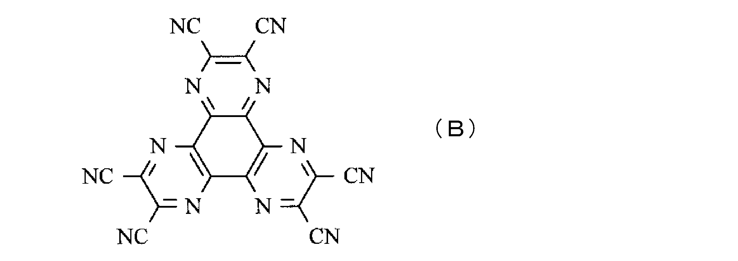
先ず、シリコン半導体基板(第1基板41)に発光素子駆動部を公知のMOSFET製造プロセスに基づき形成する。
次いで、CVD法に基づき全面に基体26を形成する。
次に、トランジスタ20の一方のソース/ドレイン領域の上方に位置する基体26の部分に、フォトリソグラフィ技術及びエッチング技術に基づき接続孔を形成する。その後、接続孔を含む基体26の上に金属層を、例えば、スパッタリング法に基づき形成し、次いで、フォトリソグラフィ技術及びエッチング技術に基づき金属層をパターニングすることで、基体26の上に第1電極31を形成することができる。第1電極31は、各発光素子毎に分離されている。併せて、接続孔内に第1電極31とトランジスタ20とを電気的に接続するコンタクトホール(コンタクトプラグ)27を形成することができる。
次に、例えば、CVD法に基づき、全面に絶縁層28を形成した後、フォトリソグラフィ技術及びエッチング技術に基づき、第1電極31上の絶縁層28の一部に開口部29を形成する。開口部29の底部に第1電極31が露出している。
その後、第1電極31及び絶縁層28の上に、有機層33を、例えば、真空蒸着法やスパッタリング法といったPVD法、スピンコート法やダイコート法等のコーティング法等によって成膜する。次いで、例えば真空蒸着法等に基づき、全面に第2電極32を形成する。このようにして、第1電極31上に、有機層33及び第2電極32を形成することができる。
その後、例えばCVD法又はPVD法によって、全面に保護層34を形成する。そして、前述したとおり、保護層34の上にカラーフィルタ層51R,51G,51Bを形成する。最後に、樹脂層(封止樹脂層)35を介して、第2基板42とカラーフィルタ層51R,51G,51Bとを貼り合わせる。こうして、図18に示した有機EL表示装置を得ることができる。
第1発光素子10Rは、2つの第3発光素子10Bに隣接して配置されており、
第2発光素子10Gは、2つの第3発光素子10Bに隣接して配置されており、
2つの第3発光素子10Bのそれぞれは、第1発光素子10R及び第2発光素子10Gに隣接して配置されている。即ち、実施例2の表示装置にあっては、発光素子は、ダイアゴナル配列とされている。即ち、副画素の配列はダイアゴナル配列である。発光素子群は、例えば、矩形の領域を占める。
第1発光素子10Rは、第2発光素子10G及び第3発光素子10Bに隣接して配置されており、
第2発光素子10Gは、第1発光素子10R及び第3発光素子10Bに隣接して配置されている。尚、発光素子群は、例えば、矩形の領域を占める。
[A01]《表示装置:第1の態様》
第1発光領域、及び、第1発光領域の上方に配設された第1カラーフィルタ層を備えた第1発光素子、
第2発光領域、及び、第2発光領域の上方に配設された第2カラーフィルタ層を備えた第2発光素子、並びに、
第3発光領域、及び、第3発光領域の上方に配設された第3カラーフィルタ層を備えた第1発光素子、
から構成された発光素子群が、複数、基体上に配列されて成り、
隣接する発光素子において、カラーフィルタ層の発光領域と対向する底面の境界線と発光領域の端部とを結ぶ最短の線分が基体の法線と成す角度は、各発光素子において同じである表示装置。
[A02]《表示装置:第2の態様》
第1発光領域、及び、第1発光領域の上方に配設された第1カラーフィルタ層を備えた第1発光素子、
第2発光領域、及び、第2発光領域の上方に配設された第2カラーフィルタ層を備えた第2発光素子、並びに、
第3発光領域、及び、第3発光領域の上方に配設された第3カラーフィルタ層を備えた第1発光素子、
から構成された発光素子群が、複数、基体上に配列されて成り、
隣接する発光素子において、カラーフィルタ層の発光領域と対向する底面の境界線の基体に対する正射影像から、発光領域の端部の基体に対する正射影像までの距離は、各発光素子において同じである表示装置。
[A03]カラーフィルタ層頂面とカラーフィルタ層頂面との境界線で囲まれたカラーフィルタ層の頂面領域の基体に対する正射影像の面積は、第1発光素子、第2発光素子及び第3発光素子において同じである[A01]又は[A02]に記載の表示装置。
[A04]第1発光素子、第2発光素子及び第3発光素子において、発光領域の面積は異なる[A03]に記載の表示装置。
[A05]カラーフィルタ層頂面とカラーフィルタ層頂面との境界線で囲まれたカラーフィルタ層の頂面領域の基体に対する正射影像の面積は、第1発光素子、第2発光素子及び第3発光素子において異なる[A01]又は[A02]に記載の表示装置。
[A06]第1発光素子、第2発光素子及び第3発光素子において、発光領域の面積は同じである[A05]に記載の表示装置。
[A07]第1発光領域、第2発光領域及び第3発光領域は白色光を発光する[A01]乃至[A06]のいずれか1項に記載の表示装置。
[A08]第1発光領域は赤色光を発光し、第2発光領域は緑色光を発光し、第3発光領域は青色光を発光する[A01]乃至[A06]のいずれか1項に記載の表示装置。
[A09]複数の発光素子群を構成する第1発光素子は第1の方向に沿って配列されており、
複数の発光素子群を構成する第2発光素子は第1の方向に沿って配列されており、
複数の発光素子群を構成する第3発光素子は第1の方向に沿って配列されている[A01]乃至[A08]のいずれか1項に記載の表示装置。
[A10]発光素子群は、2×2に配列された4つの発光素子から構成されており、
第1発光素子は、2つの第3発光素子に隣接して配置されており、
第2発光素子は、2つの第3発光素子に隣接して配置されており、
2つの第3発光素子のそれぞれは、第1発光素子及び第2発光素子に隣接して配置されている[A01]乃至[A08]のいずれか1項に記載の表示装置。
[A11]発光素子群は、1つの第1発光素子、1つの第2発光素子、及び、1つの第3発光素子から構成されており、
第1発光素子は、第2発光素子及び第3発光素子に隣接して配置されており、
第2発光素子は、第1発光素子及び第3発光素子に隣接して配置されている[A01]乃至[A08]のいずれか1項に記載の表示装置。
Claims (20)
- 第1発光領域、及び、第1発光領域の上方に配設された第1カラーフィルタ層を備えた第1発光素子、
第2発光領域、及び、第2発光領域の上方に配設された第2カラーフィルタ層を備えた第2発光素子、並びに、
第3発光領域、及び、第3発光領域の上方に配設された第3カラーフィルタ層を備えた第1発光素子、
から構成された発光素子群が、複数、基体上に配列されて成り、
隣接する発光素子において、カラーフィルタ層の発光領域と対向する底面の境界線と発光領域の端部とを結ぶ最短の線分が基体の法線と成す角度は、各発光素子において同じである表示装置。 - カラーフィルタ層頂面とカラーフィルタ層頂面との境界線で囲まれたカラーフィルタ層の頂面領域の基体に対する正射影像の面積は、第1発光素子、第2発光素子及び第3発光素子において同じである請求項1に記載の表示装置。
- 第1発光素子、第2発光素子及び第3発光素子において、発光領域の面積は異なる請求項2に記載の表示装置。
- カラーフィルタ層頂面とカラーフィルタ層頂面との境界線で囲まれたカラーフィルタ層の頂面領域の基体に対する正射影像の面積は、第1発光素子、第2発光素子及び第3発光素子において異なる請求項1に記載の表示装置。
- 第1発光素子、第2発光素子及び第3発光素子において、発光領域の面積は同じである請求項4に記載の表示装置。
- 第1発光領域、第2発光領域及び第3発光領域は白色光を発光する請求項1に記載の表示装置。
- 第1発光領域は赤色光を発光し、第2発光領域は緑色光を発光し、第3発光領域は青色光を発光する請求項1に記載の表示装置。
- 複数の発光素子群を構成する第1発光素子は第1の方向に沿って配列されており、
複数の発光素子群を構成する第2発光素子は第1の方向に沿って配列されており、
複数の発光素子群を構成する第3発光素子は第1の方向に沿って配列されている請求項1に記載の表示装置。 - 発光素子群は、2×2に配列された4つの発光素子から構成されており、
第1発光素子は、2つの第3発光素子に隣接して配置されており、
第2発光素子は、2つの第3発光素子に隣接して配置されており、
2つの第3発光素子のそれぞれは、第1発光素子及び第2発光素子に隣接して配置されている請求項1に記載の表示装置。 - 発光素子群は、1つの第1発光素子、1つの第2発光素子、及び、1つの第3発光素子から構成されており、
第1発光素子は、第2発光素子及び第3発光素子に隣接して配置されており、
第2発光素子は、第1発光素子及び第3発光素子に隣接して配置されている請求項1に記載の表示装置。 - 第1発光領域、及び、第1発光領域の上方に配設された第1カラーフィルタ層を備えた第1発光素子、
第2発光領域、及び、第2発光領域の上方に配設された第2カラーフィルタ層を備えた第2発光素子、並びに、
第3発光領域、及び、第3発光領域の上方に配設された第3カラーフィルタ層を備えた第1発光素子、
から構成された発光素子群が、複数、基体上に配列されて成り、
隣接する発光素子において、カラーフィルタ層の発光領域と対向する底面の境界線の基体に対する正射影像から、発光領域の端部の基体に対する正射影像までの距離は、各発光素子において同じである表示装置。 - カラーフィルタ層頂面とカラーフィルタ層頂面との境界線で囲まれたカラーフィルタ層の頂面領域の基体に対する正射影像の面積は、第1発光素子、第2発光素子及び第3発光素子において同じである請求項11に記載の表示装置。
- 第1発光素子、第2発光素子及び第3発光素子において、発光領域の面積は異なる請求項12に記載の表示装置。
- カラーフィルタ層頂面とカラーフィルタ層頂面との境界線で囲まれたカラーフィルタ層の頂面領域の基体に対する正射影像の面積は、第1発光素子、第2発光素子及び第3発光素子において異なる請求項11に記載の表示装置。
- 第1発光素子、第2発光素子及び第3発光素子において、発光領域の面積は同じである請求項14に記載の表示装置。
- 第1発光領域、第2発光領域及び第3発光領域は白色光を発光する請求項11に記載の表示装置。
- 第1発光領域は赤色光を発光し、第2発光領域は緑色光を発光し、第3発光領域は青色光を発光する請求項11に記載の表示装置。
- 複数の発光素子群を構成する第1発光素子は第1の方向に沿って配列されており、
複数の発光素子群を構成する第2発光素子は第1の方向に沿って配列されており、
複数の発光素子群を構成する第3発光素子は第1の方向に沿って配列されている請求項11に記載の表示装置。 - 発光素子群は、2×2に配列された4つの発光素子から構成されており、
第1発光素子は、2つの第3発光素子に隣接して配置されており、
第2発光素子は、2つの第3発光素子に隣接して配置されており、
2つの第3発光素子のそれぞれは、第1発光素子及び第2発光素子に隣接して配置されている請求項11に記載の表示装置。 - 発光素子群は、1つの第1発光素子、1つの第2発光素子、及び、1つの第3発光素子から構成されており、
第1発光素子は、第2発光素子及び第3発光素子に隣接して配置されており、
第2発光素子は、第1発光素子及び第3発光素子に隣接して配置されている請求項11に記載の表示装置。
Priority Applications (5)
| Application Number | Priority Date | Filing Date | Title |
|---|---|---|---|
| DE112019006594.7T DE112019006594T5 (de) | 2019-01-08 | 2019-12-25 | Anzeigevorrichtung |
| JP2020565695A JP7525403B2 (ja) | 2019-01-08 | 2019-12-25 | 表示装置 |
| US17/296,104 US20220013588A1 (en) | 2019-01-08 | 2019-12-25 | Display device |
| KR1020217018164A KR20210113181A (ko) | 2019-01-08 | 2019-12-25 | 표시 장치 |
| CN201980087486.8A CN113261389B (zh) | 2019-01-08 | 2019-12-25 | 显示装置 |
Applications Claiming Priority (2)
| Application Number | Priority Date | Filing Date | Title |
|---|---|---|---|
| JP2019001112 | 2019-01-08 | ||
| JP2019-001112 | 2019-01-08 |
Publications (1)
| Publication Number | Publication Date |
|---|---|
| WO2020145148A1 true WO2020145148A1 (ja) | 2020-07-16 |
Family
ID=71520673
Family Applications (1)
| Application Number | Title | Priority Date | Filing Date |
|---|---|---|---|
| PCT/JP2019/050870 Ceased WO2020145148A1 (ja) | 2019-01-08 | 2019-12-25 | 表示装置 |
Country Status (7)
| Country | Link |
|---|---|
| US (1) | US20220013588A1 (ja) |
| JP (1) | JP7525403B2 (ja) |
| KR (1) | KR20210113181A (ja) |
| CN (1) | CN113261389B (ja) |
| DE (1) | DE112019006594T5 (ja) |
| TW (1) | TW202044636A (ja) |
| WO (1) | WO2020145148A1 (ja) |
Cited By (2)
| Publication number | Priority date | Publication date | Assignee | Title |
|---|---|---|---|---|
| US20220069002A1 (en) * | 2020-08-27 | 2022-03-03 | Lg Electronics Inc. | Display device using semiconductor light emitting element |
| WO2025028395A1 (ja) * | 2023-07-31 | 2025-02-06 | ソニーセミコンダクタソリューションズ株式会社 | 発光装置および電子機器 |
Families Citing this family (3)
| Publication number | Priority date | Publication date | Assignee | Title |
|---|---|---|---|---|
| US11778883B2 (en) * | 2019-08-27 | 2023-10-03 | Boe Technology Group Co., Ltd. | Display device, manufacture method, and electronic equipment |
| CN111490180A (zh) * | 2020-04-23 | 2020-08-04 | 京东方科技集团股份有限公司 | 显示面板、显示装置以及显示面板的制造方法 |
| CN112102783B (zh) * | 2020-11-05 | 2021-02-02 | 武汉华星光电半导体显示技术有限公司 | 显示装置及电子设备 |
Citations (7)
| Publication number | Priority date | Publication date | Assignee | Title |
|---|---|---|---|---|
| JP2012504852A (ja) * | 2008-10-01 | 2012-02-23 | ユニバーサル・ディスプレイ・コーポレーション | 新規のoledディスプレイ構造 |
| JP2013175433A (ja) * | 2012-01-24 | 2013-09-05 | Canon Inc | 表示装置 |
| US20160322432A1 (en) * | 2015-04-30 | 2016-11-03 | Novatek Microelectronics Corp. | Sub-pixel arrangement structure of organic light emitting diode display |
| JP2018081831A (ja) * | 2016-11-17 | 2018-05-24 | セイコーエプソン株式会社 | 電気光学装置、電気光学装置の製造方法、及び、電子機器 |
| JP2018124540A (ja) * | 2017-02-01 | 2018-08-09 | セイコーエプソン株式会社 | 電気光学装置、電子機器、ヘッドマウントディスプレイ |
| CN108493211A (zh) * | 2017-12-28 | 2018-09-04 | 友达光电股份有限公司 | 显示面板 |
| JP2019029188A (ja) * | 2017-07-31 | 2019-02-21 | セイコーエプソン株式会社 | 電気光学装置 |
Family Cites Families (23)
| Publication number | Priority date | Publication date | Assignee | Title |
|---|---|---|---|---|
| JP2008225179A (ja) * | 2007-03-14 | 2008-09-25 | Sony Corp | 表示装置、表示装置の駆動方法、および電子機器 |
| JP5293497B2 (ja) * | 2009-08-18 | 2013-09-18 | ソニー株式会社 | 表示装置 |
| JP5445364B2 (ja) * | 2010-07-09 | 2014-03-19 | セイコーエプソン株式会社 | 有機el装置、有機el装置の製造方法、ならびに電子機器 |
| JP5919807B2 (ja) | 2011-03-30 | 2016-05-18 | ソニー株式会社 | 有機発光素子、有機発光素子の製造方法および表示装置 |
| JP5741274B2 (ja) * | 2011-07-22 | 2015-07-01 | セイコーエプソン株式会社 | 有機el装置及び電子機器 |
| JP2013152853A (ja) | 2012-01-25 | 2013-08-08 | Canon Inc | 表示装置 |
| JP6019997B2 (ja) * | 2012-09-26 | 2016-11-02 | ソニー株式会社 | 表示装置および電子機器 |
| JP6186698B2 (ja) | 2012-10-29 | 2017-08-30 | セイコーエプソン株式会社 | 有機el装置、電子機器 |
| JP6111643B2 (ja) * | 2012-12-17 | 2017-04-12 | セイコーエプソン株式会社 | 有機エレクトロルミネッセンス装置、及び電子機器 |
| US20140339606A1 (en) * | 2013-05-16 | 2014-11-20 | Visera Technologies Company Limited | Bsi cmos image sensor |
| JP2015069700A (ja) * | 2013-09-26 | 2015-04-13 | 株式会社ジャパンディスプレイ | 表示装置 |
| JP6318676B2 (ja) * | 2014-02-14 | 2018-05-09 | セイコーエプソン株式会社 | 有機発光装置の製造方法、有機発光装置、及び電子機器 |
| JP2017147059A (ja) * | 2016-02-15 | 2017-08-24 | セイコーエプソン株式会社 | 電気光学装置及び電子機器 |
| JP6680565B2 (ja) * | 2016-02-29 | 2020-04-15 | 株式会社ジャパンディスプレイ | 表示装置、及び、表示装置の製造方法 |
| CN107275360B (zh) * | 2016-04-01 | 2020-10-16 | 乐金显示有限公司 | 有机发光显示装置 |
| JP6299845B1 (ja) * | 2016-11-15 | 2018-03-28 | セイコーエプソン株式会社 | 電気光学装置、電気光学装置の製造方法、及び、電子機器 |
| CN108305565B (zh) * | 2017-01-11 | 2020-06-30 | 刘敏钻 | 显示装置 |
| CN107275502B (zh) * | 2017-06-29 | 2019-11-12 | 上海天马有机发光显示技术有限公司 | 有机发光显示面板和显示装置 |
| KR102367247B1 (ko) * | 2017-07-04 | 2022-02-25 | 삼성디스플레이 주식회사 | 표시 장치 |
| US10353243B2 (en) * | 2017-08-01 | 2019-07-16 | Innolux Corporation | Display device |
| US10367020B2 (en) * | 2017-11-15 | 2019-07-30 | Taiwan Semiconductor Manufacturing Co., Ltd. | Polarizers for image sensor devices |
| KR102759192B1 (ko) * | 2019-05-24 | 2025-01-31 | 삼성디스플레이 주식회사 | 표시모듈 |
| WO2023095658A1 (ja) * | 2021-11-26 | 2023-06-01 | ソニーセミコンダクタソリューションズ株式会社 | 発光装置及び電子機器 |
-
2019
- 2019-12-25 KR KR1020217018164A patent/KR20210113181A/ko not_active Ceased
- 2019-12-25 US US17/296,104 patent/US20220013588A1/en active Pending
- 2019-12-25 DE DE112019006594.7T patent/DE112019006594T5/de active Pending
- 2019-12-25 JP JP2020565695A patent/JP7525403B2/ja active Active
- 2019-12-25 CN CN201980087486.8A patent/CN113261389B/zh active Active
- 2019-12-25 WO PCT/JP2019/050870 patent/WO2020145148A1/ja not_active Ceased
- 2019-12-30 TW TW108148291A patent/TW202044636A/zh unknown
Patent Citations (7)
| Publication number | Priority date | Publication date | Assignee | Title |
|---|---|---|---|---|
| JP2012504852A (ja) * | 2008-10-01 | 2012-02-23 | ユニバーサル・ディスプレイ・コーポレーション | 新規のoledディスプレイ構造 |
| JP2013175433A (ja) * | 2012-01-24 | 2013-09-05 | Canon Inc | 表示装置 |
| US20160322432A1 (en) * | 2015-04-30 | 2016-11-03 | Novatek Microelectronics Corp. | Sub-pixel arrangement structure of organic light emitting diode display |
| JP2018081831A (ja) * | 2016-11-17 | 2018-05-24 | セイコーエプソン株式会社 | 電気光学装置、電気光学装置の製造方法、及び、電子機器 |
| JP2018124540A (ja) * | 2017-02-01 | 2018-08-09 | セイコーエプソン株式会社 | 電気光学装置、電子機器、ヘッドマウントディスプレイ |
| JP2019029188A (ja) * | 2017-07-31 | 2019-02-21 | セイコーエプソン株式会社 | 電気光学装置 |
| CN108493211A (zh) * | 2017-12-28 | 2018-09-04 | 友达光电股份有限公司 | 显示面板 |
Cited By (3)
| Publication number | Priority date | Publication date | Assignee | Title |
|---|---|---|---|---|
| US20220069002A1 (en) * | 2020-08-27 | 2022-03-03 | Lg Electronics Inc. | Display device using semiconductor light emitting element |
| US12154935B2 (en) * | 2020-08-27 | 2024-11-26 | Lg Electronics Inc. | Display device using semiconductor light emitting element and black dye layers |
| WO2025028395A1 (ja) * | 2023-07-31 | 2025-02-06 | ソニーセミコンダクタソリューションズ株式会社 | 発光装置および電子機器 |
Also Published As
| Publication number | Publication date |
|---|---|
| CN113261389A (zh) | 2021-08-13 |
| CN113261389B (zh) | 2025-04-08 |
| TW202044636A (zh) | 2020-12-01 |
| JP7525403B2 (ja) | 2024-07-30 |
| KR20210113181A (ko) | 2021-09-15 |
| DE112019006594T5 (de) | 2021-12-23 |
| US20220013588A1 (en) | 2022-01-13 |
| JPWO2020145148A1 (ja) | 2021-11-18 |
Similar Documents
| Publication | Publication Date | Title |
|---|---|---|
| JP7841552B2 (ja) | 表示装置 | |
| JP7057147B2 (ja) | 発光素子及び表示装置 | |
| JP7736687B2 (ja) | 表示装置 | |
| US12366685B2 (en) | Light emitting element, display device, and method for manufacturing display device | |
| WO2020162355A1 (ja) | 発光素子及び表示装置 | |
| JP7525403B2 (ja) | 表示装置 | |
| WO2017051622A1 (ja) | 表示装置及びその製造方法 | |
| JP7509860B2 (ja) | 発光素子ユニット | |
| WO2017212797A1 (ja) | 発光素子、及び、発光素子を備えた表示装置 | |
| US12412529B2 (en) | Display device | |
| WO2022102434A1 (ja) | 表示装置 | |
| WO2020110944A1 (ja) | 発光素子、表示装置及び電子機器 |
Legal Events
| Date | Code | Title | Description |
|---|---|---|---|
| 121 | Ep: the epo has been informed by wipo that ep was designated in this application |
Ref document number: 19909043 Country of ref document: EP Kind code of ref document: A1 |
|
| ENP | Entry into the national phase |
Ref document number: 20217018164 Country of ref document: KR Kind code of ref document: A |
|
| ENP | Entry into the national phase |
Ref document number: 2020565695 Country of ref document: JP Kind code of ref document: A |
|
| 122 | Ep: pct application non-entry in european phase |
Ref document number: 19909043 Country of ref document: EP Kind code of ref document: A1 |
|
| WWG | Wipo information: grant in national office |
Ref document number: 201980087486.8 Country of ref document: CN |