WO2020145003A1 - 積層体 - Google Patents
積層体 Download PDFInfo
- Publication number
- WO2020145003A1 WO2020145003A1 PCT/JP2019/048297 JP2019048297W WO2020145003A1 WO 2020145003 A1 WO2020145003 A1 WO 2020145003A1 JP 2019048297 W JP2019048297 W JP 2019048297W WO 2020145003 A1 WO2020145003 A1 WO 2020145003A1
- Authority
- WO
- WIPO (PCT)
- Prior art keywords
- layer
- peeling
- metal layer
- metal
- less
- Prior art date
- Legal status (The legal status is an assumption and is not a legal conclusion. Google has not performed a legal analysis and makes no representation as to the accuracy of the status listed.)
- Ceased
Links
Images



Classifications
-
- B—PERFORMING OPERATIONS; TRANSPORTING
- B32—LAYERED PRODUCTS
- B32B—LAYERED PRODUCTS, i.e. PRODUCTS BUILT-UP OF STRATA OF FLAT OR NON-FLAT, e.g. CELLULAR OR HONEYCOMB, FORM
- B32B15/00—Layered products comprising a layer of metal
- B32B15/04—Layered products comprising a layer of metal comprising metal as the main or only constituent of a layer, which is next to another layer of the same or of a different material
Definitions
- the present invention relates to a laminate including a carrier, a metal layer, etc. (for example, a copper foil with a carrier).
- the coreless build-up method is a method in which insulating layers and wiring layers are alternately laminated (build-up) to form a multilayer structure without using a so-called core substrate.
- the coreless build-up method it has been proposed to use a laminate having a metal layer on a carrier provided with a peeling function so that the support can be easily peeled from the multilayer printed wiring board.
- Patent Document 1 Japanese Unexamined Patent Publication No.
- a copper foil with a carrier is used as a laminate, and an insulating resin layer is attached to the carrier surface of this copper foil with a carrier to form a support, Build up by forming the first wiring conductor on the ultra-thin copper layer side of the copper foil by processes such as photoresist processing, pattern electrolytic copper plating, resist removal, etc., then laminating insulating material and performing hot press processing etc.
- a method of manufacturing a package substrate for mounting a semiconductor element which includes forming a wiring layer, peeling a support substrate with a carrier, and removing an ultrathin copper layer.
- the carrier base material is the member that is finally peeled off. Therefore, for example, a predetermined releasability is required between the carrier base material and the layers forming the printed wiring board.
- a peeling functional layer having a peeling function on the surface of a carrier substrate a laminated layer including a peeling layer composed of an adhesion layer and a peeling auxiliary layer containing a metal element, and a carbon layer in order from the carrier substrate side.
- Patent Document 2 International Publication No.
- a carrier an adhesion metal layer made of a metal such as titanium, a peeling auxiliary layer made of copper, a peeling layer, and an ultrathin copper layer are sequentially arranged.
- a provided copper foil with a carrier is disclosed, and it is said that the release layer is preferably a carbon layer.
- the adhesion metal layer, the peeling auxiliary layer, the peeling layer, and the ultra-thin copper layer are formed by sputtering. It is also described to do.
- heat treatment may be performed under a temperature condition of 200° C. or higher.
- the heat treatment is performed under the temperature condition of 300° C. or more, whereby the carrier base material is peeled well. There is a problem that there is no.
- the present inventors have recently performed a fluorination treatment and/or a nitriding treatment on the metal layer-side surface of the release functional layer containing a metal element in a laminate including a carrier substrate, a release functional layer, and a metal layer in this order.
- a fluorination treatment and/or a nitriding treatment on the metal layer-side surface of the release functional layer containing a metal element in a laminate including a carrier substrate, a release functional layer, and a metal layer in this order.
- an object of the present invention is to provide a layered product capable of satisfactorily peeling a carrier substrate even when heat-treated under a temperature condition of 300° C. or higher.
- a laminate including a carrier substrate, a peeling function layer and a metal layer in this order,
- the peeling functional layer contains a metal element
- the surface of the peeling functional layer on the side of the metal layer is a fluorinated surface and/or a nitriding surface, and the peeling functional layer has a total content of fluorine and nitrogen of 1.0 atomic% or more.
- a laminate is provided, wherein the region is over a thickness of 10 nm or more.
- FIG. 4 is a graph showing the peel strength after heating at various temperatures for 1 hour in the conventional laminated body shown in FIG. 3.
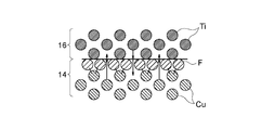
- FIG. 4 is an enlarged view of a region between a peeling auxiliary layer and a metal layer in the conventional laminated body shown in FIG. 3.
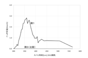
- FIG. 3 shows the result of the fluorine quantitative value by XPS of the laminated body produced in Example 1 and Example 3.
- the laminate 10 of the present invention includes a carrier substrate 12, a peeling functional layer 14, and a metal layer 16 in this order.
- the peeling function layer 14 is a layer containing a metal element, and is provided on the carrier base material 12.
- the surface of the peeling functional layer 14 on the metal layer 16 side is a fluorinated surface and/or a nitriding surface.
- the peeling function layer 14 has a region in which the sum of the content of fluorine and the content of nitrogen is 1.0 atomic% or more over a thickness of 10 nm or more.
- Each of the peeling function layer 14 and the metal layer 16 may be a single layer composed of one layer, or may be a multilayer composed of two or more layers as shown in FIG. Further, the above-mentioned various layers may be sequentially provided on both surfaces of the carrier substrate 12 so as to be vertically symmetrical.
- the laminated body 10 of the present invention is used for various purposes, and is preferably used for producing a printed wiring board.
- heat treatment may be performed under a temperature condition of, for example, 200° C. or more when forming a layer or the like constituting the printed wiring board on the carrier base material.
- the laminated body used as the copper foil with the carrier may be hot-pressed each time an insulating material is laminated.
- the temperature depends on the curing temperature of the insulating material to be laminated.
- the heat treatment is performed at a temperature of 300° C. or higher, which causes a problem that the carrier base material is not peeled off well.
- FIG. 3 shows a graph of the peel strength of the conventional laminated body 110 after heating at various temperatures for 1 hour. As shown in FIG. 4, in the conventional laminated body 110, the peel strength is excessively increased by heating at 300° C. or higher, so that the carrier substrate 112 cannot be peeled well.
- the surface of the peeling function layer 14 containing a metal element on the metal layer side is subjected to fluorination treatment and Even if the carrier base material 12 is heat-treated under a temperature condition of 300° C. or higher by performing a nitriding treatment to allow a region containing fluorine and/or nitrogen in a predetermined ratio to exist, the carrier base material 12 is good. Can be peeled off. This mechanism is not necessarily clear, but one of the factors is as follows.
- the metal layer 16 side of the peeling functional layer 14 is a copper layer
- the surface of the peeling functional layer 14 on the metal layer 16 side is a fluorinated surface
- a laminate in which at least the peeling function layer 14 side of the metal layer 16 is a titanium layer will be described.
- the fluorine in the peeling function layer 14 exists in the form of copper fluoride (CuF 2 ) on the metal layer 16 side of the peeling function layer 14.
- fluorine and copper are strongly bonded by ionic bond, while the bond between fluorine and titanium is weak with van der Waals force. Therefore, when the carrier base material 12 is peeled off without performing heat treatment such as annealing, it is peeled from between the titanium layer of the metal layer 16 and the fluorinated surface of the peeling function layer 14. Further, even when heat treatment is performed at a high temperature for a long time such as annealing at 400° C. for 2 hours, fluorine does not move to the titanium side and can remain between the titanium layer and the copper layer.
- copper fluoride is more thermally stable than titanium fluoride (TiF 4 ) which is a compound of fluorine and titanium. That is, while the sublimation temperature of titanium fluoride is 284° C., the boiling point of copper fluoride is 950° C., which is much higher. Therefore, it is considered that during the heat treatment, fluorine does not break the bond with copper and bond with titanium to sublime.
- the second reason why fluorine remains between the titanium layer and the copper layer is that the bonding force of fluorine is extremely strong. That is, since fluorine has a high electronegativity, it is extremely strongly bonded to copper, and therefore, it is considered that it remains as copper fluoride even after the heat treatment. Therefore, as shown in FIG.
- the copper fluoride existing on the surface of the peeling function layer 14 on the metal layer 16 side serves as a barrier, and diffusion of copper from the peeling function layer 14 to the metal layer 16 and from the metal layer 16
- the diffusion of titanium into the peeling function layer 14 can be suppressed.
- the carrier base material 12 is satisfactorily removed from between the metal layer 16 and the peeling function layer 14 as in the case where the heat treatment is not performed. It can be peeled off.
- the surface of the peeling function layer 14 on the metal layer 16 side is a fluorinated surface and/or a nitrided surface, and preferably a fluorinated surface. Therefore, the peeling function layer 14 contains fluorine and/or nitrogen to some extent.
- a region in which the sum of the content of fluorine and the content of nitrogen is 1.0 atom% or more (hereinafter, referred to as “(F+N) region”) has a thickness of 10 nm or more. Present, preferably over 20 nm, more preferably over 30 nm, even more preferably over 40 nm, particularly preferably over 50 nm.
- a region in which the sum of the content of fluorine and the content of nitrogen is 2.0 atomic% or more is present over a thickness of 5 nm or more, more preferably 10 nm or more, further It is preferably present over a thickness of 20 nm or more, even more preferably 30 nm or more, particularly preferably 40 nm or more, most preferably 50 nm or more.
- the sum of the content of fluorine and the content of nitrogen on the fluorinated surface and/or the nitriding surface is 1.0 atom% or more (more preferably 2.0 atom% or more).
- the (F+N) region exists on the metal layer 16 side of the peeling function layer 14.
- the upper limit of the sum of the content of fluorine and the content of nitrogen in the (F+N) region of the peeling functional layer 14 is typically 20 atom %, more typically 10 atom %, and further typically 5 It is atomic %.
- the upper limit of the thickness of the (F+N) region in the peeling functional layer 14 is not particularly limited and may be the same as the thickness of the peeling functional layer 14, but typically the thickness of the peeling functional layer 14 is 80% of the thickness of the release functional layer 14 and more typically 40% of the thickness of the release functional layer 14.
- the content of fluorine alone preferably falls within the above range. That is, in the peeling functional layer 14, it is preferable that a region having a fluorine content of 1.0 atomic% or more (hereinafter referred to as “F region”) is present over a thickness of 10 nm or more, and the above-mentioned (F+N
- F region a region having a fluorine content of 1.0 atomic% or more
- F+N The preferred (or typical) aspects of the () region apply directly to the F region.
- the fluorinated surface can be preferably formed by reactive ion etching (RIE) using a reactive gas containing fluorine such as carbon tetrafluoride or sulfur hexafluoride.
- the nitrogen content alone preferably falls within the above range. That is, in the peeling function layer 14, it is preferable that a region having a nitrogen content of 1.0 atomic% or more (hereinafter referred to as “N region”) exists over a thickness of 10 nm or more, and the above-mentioned (F+N).
- N region a region having a nitrogen content of 1.0 atomic% or more
- F+N the above-mentioned
- the preferred (or typical) aspects of the () region also apply directly to the N region.
- the nitriding surface can be preferably formed by reactive ion etching (RIE) or reactive sputtering.
- the thicknesses of the (F+N) region, the F region, and the N region (converted to SiO 2 ) of the peeling functional layer 14 are the depth direction elemental analysis of the stacked body 10 using XPS, as referred to in Examples described later. Can be specified by performing. In the depth direction elemental analysis using XPS, even if the same etching conditions are used, the etching rate varies depending on the type of material, so the thickness of the (F+N) region, the F region, and the N region itself Is difficult to obtain. Therefore, as the thickness of each region, the SiO 2 -converted thickness calculated from the time required for etching is used by utilizing the etching rate calculated from the SiO 2 film having a known film thickness. By doing so, the thickness can be uniquely determined, and thus quantitative evaluation becomes possible.
- the peeling functional layer 14 is a layer containing a metal element that enables the carrier substrate 12 to be peeled off.
- the metal element contained in the peeling function layer 14 preferably has a negative standard electrode potential.
- the peeling functional layer 14 may be a single layer composed of one layer or a multilayer composed of two or more layers.
- the peeling functional layer 14 includes a first peeling functional layer 14a provided adjacent to the carrier substrate 12 and a carrier of the first peeling functional layer 14a.
- the second peeling function layer 14b provided on the side opposite to the base material 12 is included. Another intervening layer may be present between the first peeling functional layer 14a and the second peeling functional layer 14b.
- the total thickness of the release functional layer 14 is preferably 10 nm or more and 1000 nm or less, more preferably 30 nm or more and 500 nm or less, further preferably 50 nm or more and 400 nm or less, and particularly preferably 100 nm or more and 300 or less.
- the thickness of the peeling functional layer 14 can be measured by analyzing the layer cross section with an energy dispersive X-ray spectroscopic analyzer (TEM-EDX) of a transmission electron microscope.
- TEM-EDX energy dispersive X-ray spectroscopic analyzer
- the first peeling functional layer 14a which is provided as desired, preferably contains the metal M 1 having a negative standard electrode potential, from the viewpoint of ensuring adhesion with the carrier substrate 12.
- M 1 include titanium, chromium, nickel, cobalt, aluminum, molybdenum and combinations thereof (for example, alloys and intermetallic compounds), more preferably titanium, nickel, cobalt, aluminum, molybdenum and their combinations.
- the first peeling functional layer 14a may contain an element other than M 1 within a range not impairing the adhesiveness with the carrier substrate 12.
- the content of M 1 in the first peeling functional layer 14a is preferably 50 atom% or more, more preferably 60 atom% or more, further preferably 70 atom% or more, particularly preferably 80 atom%. As described above, most preferably it is 90 atomic% or more. On the other hand, the content of M 1 in the first peeling functional layer 14a can be 100 atomic% or less.
- the metal forming the first peeling function layer 14a may contain unavoidable impurities caused by the raw material components, the film forming process, and the like. In addition, although not particularly limited, when exposed to the air after the formation of the first peeling function layer 14a, the presence of oxygen mixed in due to it is allowed.
- the first peeling functional layer 14a is preferably a layer formed by a physical vapor deposition (PVD) method, more preferably a layer formed by sputtering. It is particularly preferable that the first peeling functional layer 14a is a layer formed by a magnetron sputtering method using a metal target, since the uniformity of the film thickness distribution can be improved.
- the thickness of the first peeling functional layer 14a is preferably 5.0 nm or more and 500 nm or less, preferably 10 nm or more and 400 nm or less, more preferably 30 nm or more and 300 nm or less, further preferably 40 nm or more and 200 nm or less, particularly preferably 50 nm or more. It is 100 nm or less.
- the second peeling functional layer 14b which is provided as desired, preferably contains a metal M 2 other than the alkali metal and the alkaline earth metal from the viewpoint of controlling the peeling strength from the metal layer 16 to a desired value, and M 2 is M. Preferably it is a metal different from 1 .
- M 2 examples include copper, silver, tin, zinc, titanium, aluminum, niobium, zirconium, tungsten, tantalum, molybdenum and combinations thereof (for example, alloys and intermetallic compounds), more preferably copper, Silver, tin, zinc, titanium, aluminum, molybdenum and combinations thereof, more preferably copper, silver, titanium, aluminum, molybdenum and combinations thereof, particularly preferably copper, silver, aluminum and combinations thereof, most preferably copper.
- the second peeling functional layer 14b may contain an element other than M 2 as long as the peeling property of the carrier substrate 12 is not impaired.
- the content of M 2 in the second peeling functional layer 14b is preferably 50 atomic% or more, more preferably 60 atomic% or more, further preferably 70 atomic% or more, particularly preferably 80 atomic%. As described above, most preferably it is 90 atomic% or more.
- the content rate of M 2 in the second peeling functional layer 14b can be 100 atomic% or less.
- the metal forming the second peeling function layer 14b may contain unavoidable impurities caused by the raw material components and the film forming process. In addition, although not particularly limited, when exposed to the atmosphere after forming the second peeling function layer 14b, the presence of oxygen mixed in due to it is allowed.
- the second peeling functional layer 14b is preferably a layer formed by a physical vapor deposition (PVD) method, more preferably a layer formed by sputtering. It is particularly preferable that the second peeling function layer 14b is a layer formed by a magnetron sputtering method using a metal target, because the uniformity of the film thickness distribution can be improved.
- the thickness of the second peeling functional layer 14b is preferably 5.0 nm or more and 990 nm or less, preferably 20 nm or more and 800 nm or less, more preferably 50 nm or more and 500 nm or less, further preferably 100 nm or more and 300 nm or less, particularly preferably 150 nm or more. It is 250 nm or less.
- M 1 is titanium, nickel, aluminum or molybdenum
- M 2 is copper, silver, titanium, aluminum or molybdenum. More preferably, M 1 is titanium, nickel or molybdenum, and M 2 is copper, silver or aluminum. Particularly preferably, M 1 is titanium and M 2 is copper. By doing so, it becomes easier to impart the above-described desired peel strength to the laminate 10.
- the optional intervening layer can be the alloy of M 1 and M 2 described above. Therefore, the preferable combination of M 1 and M 2 described above is directly applicable to the preferable combination of M 1 and M 2 that form the intervening layer.
- the thickness of the intervening layer is preferably 10 nm or more and 1000 nm or less, preferably 30 nm or more and 500 nm or less, more preferably 50 nm or more and 400 nm or less, further preferably 100 nm or more and 300 nm or less, and particularly preferably 150 nm or more and 250 nm or less.
- the peeling functional layer 14 has a single-layer structure
- the above-mentioned first peeling functional layer 14a may be used as it is as an intermediate layer
- the first peeling functional layer 14a and the second peeling functional layer 14b may be formed as one layer. It may be replaced by an intermediate alloy layer of the layer.
- This intermediate alloy layer can be an alloy of M 1 and M 2 . Therefore, the preferable combination of M 1 and M 2 described above is directly applicable to the preferable combination of M 1 and M 2 forming the intermediate alloy layer.
- the thickness of the intermediate alloy layer is preferably based on the total thickness of the peeling function layer 14 described above.
- the material of the carrier substrate 12 may be any of glass, ceramics, silicon, resin, and metal, and can be appropriately selected according to the application of the laminated body 10.
- the carrier substrate 12 is a glass substrate, a ceramic substrate or a silicon wafer.
- the form of the carrier substrate 12 may be any of sheet, film, plate, and foil.
- the carrier substrate 12 may be a laminate of these sheets, films, plates, foils and the like.
- the carrier substrate 12 may be a glass plate, a ceramics plate, a silicon wafer, a metal plate, or the like that can function as a rigid support, or a metal foil, a resin film, or the like that does not have rigidity. It may be.
- Preferred examples of the metal of the carrier substrate 12 include copper, titanium, nickel, stainless steel, aluminum and the like.
- Preferred examples of ceramics include alumina, zirconia, silicon nitride, aluminum nitride, and various fine ceramics.
- Preferred examples of the resin include polyethylene terephthalate (PET), polyethylene naphthalate (PEN), polyamide, polyimide, nylon, liquid crystal polymer, polyether ether ketone (PEEK (registered trademark)), polyamide imide, polyether sulfone, Examples thereof include polyphenylene sulfide, polytetrafluoroethylene (PTFE), ethylene tetrafluoroethylene (ETFE) and the like.
- CTE coefficient of thermal expansion
- examples of such materials include low thermal expansion resins such as polyimide and liquid crystal polymers, glass, silicon and ceramics.
- the Vickers hardness of the carrier substrate 12 is preferably 100 HV or more, and more preferably 150 HV or more.
- the Vickers hardness of the carrier base material 12 can be set to 2500 HV or less, for example.
- the carrier substrate 12 is preferably composed of a resin film, glass, silicon or ceramics, particularly preferably composed of glass, silicon or ceramics, and particularly composed of glass. Is preferred.
- the carrier substrate 12 made of glass include a glass sheet.
- glass is used as the carrier substrate 12, it is lightweight, has a low coefficient of thermal expansion, has a high insulating property, and is rigid and has a flat surface, so that it has the advantages that the surface of the metal layer 16 can be extremely smooth.
- the carrier base material 12 is glass, using the laminate 10 as a carrier-attached copper foil for producing a printed wiring board has various advantages.
- the glass constituting the carrier substrate 12 include quartz glass, borosilicate glass, non-alkali glass, soda lime glass, aluminosilicate glass, and combinations thereof, and particularly preferably non-alkali glass. ..
- Alkali-free glass is a glass that contains silicon dioxide, aluminum oxide, boron oxide, and an alkaline earth metal oxide such as calcium oxide or barium oxide as a main component, and further contains boric acid and does not substantially contain an alkali metal. It means that.
- This alkali-free glass has a low coefficient of thermal expansion in a wide temperature range from 0° C. to 350° C. and is stable in a range of, for example, 3 ppm/K or more and 5 ppm/K or less. Therefore, when a semiconductor chip is mounted as an electronic element, There is an advantage that the warp of the glass can be minimized.
- the thickness of the carrier substrate 12 is, for example, preferably 100 ⁇ m or more and 2000 ⁇ m or less, more preferably 300 ⁇ m or more and 1800 ⁇ m or less, and further preferably 400 ⁇ m or more and 1100 ⁇ m or less. With the thickness within such a range, it is possible to realize a thin printed wiring board and a reduction in warpage that occurs when electronic components are mounted, while ensuring an appropriate strength that does not hinder handling. ..
- the arithmetic mean roughness Ra of the surface of the carrier substrate 12 on the side of the peeling function layer 14 is preferably 0.1 nm or more and 70 nm or less, more preferably 0.5 nm or more and 60 nm or less, and further preferably 1.0 nm or more and 50 nm or less. , Particularly preferably 1.5 nm or more and 40 nm or less, most preferably 2.0 nm or more and 30 nm or less.
- the highly miniaturized wiring pattern is, for example, designed such that the line/space (L/S) is 13 ⁇ m or less/13 ⁇ m or less, specifically, in the range of 2 ⁇ m/2 ⁇ m or more and 12 ⁇ m/12 ⁇ m or less.
- the arithmetic mean roughness Ra can be measured by a method based on JIS B 0601-2001.
- the metal layer 16 is a layer made of metal.
- the metal layer 16 may have a one-layer structure or a two-layer structure or more. When the metal layer 16 is composed of two or more layers, the metal layer 16 is formed on the surface of the peeling function layer 14 opposite to the carrier substrate 12 from the first metal layer 16a to the m-th metal layer (m). Can be a structure in which metal layers up to an integer of 2) are sequentially stacked.
- the total thickness of the metal layer 16 is preferably 100 nm or more and 2000 nm or less, preferably 150 nm or more and 1500 nm or less, more preferably 200 nm or more and 1000 nm or less, further preferably 300 nm or more and 800 nm or less, and particularly preferably 350 nm or more and 500 nm or less. ..
- the thickness of the metal layer 16 can be measured by analyzing the cross section of the layer with an energy dispersive X-ray spectroscopic analyzer (TEM-EDX) of a transmission electron microscope.
- TEM-EDX energy dispersive X-ray spectroscopic analyzer
- the first metal layer 16a is not particularly limited as long as it gives the laminate 10 a desired function such as an etching stopper function or an antireflection function.
- the metal forming the first metal layer 16a include titanium, aluminum, niobium, zirconium, chromium, tungsten, tantalum, cobalt, silver, nickel, molybdenum, and combinations thereof, more preferably titanium or zirconium.
- the first metal layer 16a becomes a layer that is less likely to be etched by the flash etching solution than the second metal layer 16b described later, and thus can function as an etching stopper layer. Further, since the above-described metal forming the first metal layer 16a also has a function of preventing light reflection, the first metal layer 16a improves visibility in image inspection (for example, automatic image inspection (AOI)). Can also function as an antireflection layer.
- the first metal layer 16a may be a pure metal or an alloy.
- the metal forming the first metal layer 16a may include inevitable impurities caused by the raw material components, the film forming process, and the like.
- the upper limit of the metal content is not particularly limited and may be 100 atom %.
- the first metal layer 16a is preferably a layer formed by physical vapor deposition (PVD) method, and more preferably a layer formed by sputtering.
- the thickness of the first metal layer 16a is preferably 1 nm or more and 500 nm or less, more preferably 10 nm or more and 400 nm or less, further preferably 30 nm or more and 300 nm or less, and particularly preferably 50 nm or more and 200 nm or less.
- the metal forming the second metal layer 16b include transition elements of Group 4, Group 5, Group 6, Group 9, Group 10 and Group 11, aluminum, and combinations thereof (for example, Alloys and intermetallic compounds), more preferably copper, gold, titanium, aluminum, niobium, zirconium, chromium, tungsten, tantalum, cobalt, silver, nickel, molybdenum and combinations thereof, more preferably copper, gold, Titanium, aluminum, niobium, zirconium, cobalt, silver, nickel, molybdenum and combinations thereof, even more preferably copper, gold, titanium, aluminum, silver, molybdenum and combinations thereof, particularly preferably copper, gold, titanium, molybdenum. And combinations thereof, most preferably copper.
- the second metal layer 16b may be manufactured by any method, for example, a wet film forming method such as an electroless metal plating method or an electrolytic metal plating method, or a physical vapor deposition (PVD) method such as sputtering or vacuum evaporation. It may be a metal foil formed by chemical vapor deposition, or a combination thereof.
- the particularly preferable second metal layer 16b is a metal layer formed by a physical vapor deposition (PVD) method such as a sputtering method or a vacuum evaporation method from the viewpoint of easily adapting to fine pitch due to ultra-thinning, and most preferably. It is a metal layer manufactured by a sputtering method.
- the second metal layer 16b is preferably a non-roughened metal layer.
- the second metal layer 16b is preliminarily roughened, soft-etched or washed unless it interferes with the formation of a wiring pattern during manufacturing of the printed wiring board.
- the secondary roughening may be caused by the treatment or the redox treatment.
- the thickness of the second metal layer 16b is preferably 10 nm or more and 1000 nm or less, more preferably 20 nm or more and 900 nm or less, further preferably 30 nm or more and 700 nm or less, and further more It is preferably 50 nm or more and 600 nm or less, particularly preferably 70 nm or more and 500 nm or less, and most preferably 100 nm or more and 400 nm or less. It is preferable that the metal layer having a thickness within such a range is produced by a sputtering method from the viewpoints of the in-plane uniformity of the film formation thickness and the productivity in the form of a sheet or a roll.
- the surface of the second metal layer 16b opposite to the first metal layer 16a has an arithmetic average roughness Ra of 1.0 nm or more and 100 nm or less measured according to JIS B 0601-2001. Is more preferable, 2.0 nm or more and 40 nm or less, further preferably 3.0 nm or more and 35 nm or less, particularly preferably 4.0 nm or more and 30 nm or less, and most preferably 5.0 nm or more and 15 nm or less.
- the smaller the arithmetic mean roughness is, the more suitable the printed wiring board manufactured by using the laminated body 10 is, for example, to form a highly miniaturized wiring pattern.
- the highly miniaturized wiring pattern is, for example, designed such that the line/space (L/S) is 13 ⁇ m or less/13 ⁇ m or less, specifically, in the range of 2 ⁇ m/2 ⁇ m or more and 12 ⁇ m/12 ⁇ m or less. Refers to the wiring pattern.
- the metal layer 16 has a single-layer structure, it is preferable to employ the above-mentioned second metal layer 16b as the metal layer 16 as it is.
- the metal layer 16 has an n-layer structure (n is an integer of 3 or more)
- the first metal layer 16a to the (n-1)th metal layer 16a of the metal layer 16 are described above. It is preferable that the outermost layer of the metal layer 16, that is, the nth metal layer has the above-described second metal layer 16b.
- the laminate 10 preferably has a peel strength between the peeling functional layer 14 and the metal layer 16 within a desired range when a heat history of 300° C. or higher is applied to the laminate 10.
- the specific peel strength is preferably 1.0 gf/cm or more and 50 gf/cm or less, more preferably 2.0 gf/cm or more and 30 gf/cm or less, and further preferably 3.0 gf/cm or more and 20 gf/cm or less. Is. More specifically, when the laminate 10 is subjected to a heat history of 400° C. for 2 hours, the peel strength between the peeling functional layer 14 and the metal layer 16 is preferably within the above range. .. When the peeling strength is within the above range, it is possible to maintain a predetermined peeling strength and enable good peeling in the peeling step. This peel strength can be measured according to JIS Z 0237-2009.
- the laminate 10 according to the present invention can be produced by preparing the carrier base material 12 and forming the peeling function layer 14 and the metal layer 16 on the carrier base material 12.
- the peeling functional layer 14 is formed by forming a layer constituting the peeling functional layer 14 on the carrier substrate 12 by a physical vapor deposition (PVD) method, and then forming a surface of the peeling functional layer 14 opposite to the carrier substrate 12. This can be preferably carried out by treating the side with reactive ion etching.
- the formation of the metal layer 16 is preferably performed by the physical vapor deposition (PVD) method from the viewpoint of easily adapting to fine pitch due to ultra-thinning.
- PVD physical vapor deposition
- sputtering methods examples include sputtering methods, vacuum deposition methods, and ion plating methods.
- the sputtering method is preferably used because the film thickness can be controlled in a wide range of 0.05 nm to 5000 nm and the film thickness uniformity can be ensured over a wide width or area.
- the film formation by the physical vapor deposition (PVD) method may be performed according to known conditions using a known vapor phase film forming apparatus and is not particularly limited.
- the sputtering method various known methods such as a magnetron sputtering method, a two-pole sputtering method, and a facing target sputtering method can be used.
- the magnetron sputtering method is preferable because the film formation rate is high and the productivity is high.
- the sputtering method may be performed with either DC (direct current) or RF (high frequency) power source.
- a plate type target whose target shape is widely known can be used. Above all, it is desirable to use a cylindrical target from the viewpoint of target use efficiency.
- the peeling functional layer 14 is formed by a physical vapor deposition (PVD) method, the fluorinated surface is formed by reactive ion etching on the surface of the peeling functional layer 14 opposite to the carrier substrate 12, and the metal layer 16 is formed. Film formation by the physical vapor deposition (PVD) method will be described.
- the peeling functional layer 14 is composed of the first peeling functional layer 14a and the second peeling functional layer 14b, and the metal layer 16 is composed of the first metal layer 16a and the second metal layer 16b. Shall be configured.
- the film formation of the first peeling functional layer 14a by a physical vapor deposition (PVD) method is performed by a magnetron sputtering method in a non-oxidizing atmosphere using the target composed of the metal M 1 described above. It is preferable that the film thickness distribution can be improved.
- the purity of the target is preferably 99.9% or higher.
- the gas used for sputtering include an inert gas such as argon gas.
- the flow rate of the argon gas can be appropriately determined according to the size of the sputtering chamber and the film forming conditions.
- the pressure during film formation is preferably 0.1 Pa or more and 20 Pa or less from the viewpoint of suppressing the occurrence of operation failures such as abnormal discharge and plasma irradiation failure and continuously forming a film.
- This pressure range can be set by adjusting the film forming power and the flow rate of the argon gas according to the apparatus structure, capacity, vacuum pump exhaust capacity, film forming power supply rated capacity, and the like.
- the sputtering power can be deposited in film thickness uniformity, in consideration of productivity and the like 0.05 W / cm 2 or more per unit surface area of the target 10.0 W / cm 2 or less.
- the film formation of the second peeling functional layer 14b by the physical vapor deposition (PVD) method is performed by the magnetron sputtering method in a non-oxidizing atmosphere using the target composed of the metal M 2 described above. It is preferable that the film thickness distribution can be improved.
- the purity of the target is preferably 99.9% or higher.
- the gas used for sputtering include an inert gas such as argon gas. The flow rate of the argon gas can be appropriately determined according to the size of the sputtering chamber and the film forming conditions.
- the pressure during film formation is preferably 0.1 Pa or more and 20 Pa or less from the viewpoint of suppressing the occurrence of operation failures such as abnormal discharge and plasma irradiation failure and continuously forming a film.
- This pressure range can be set by adjusting the film forming power and the flow rate of the argon gas according to the apparatus structure, capacity, vacuum pump exhaust capacity, film forming power supply rated capacity, and the like.
- the sputtering power can be deposited in film thickness uniformity, in consideration of productivity and the like 0.05 W / cm 2 or more per unit surface area of the target 10.0 W / cm 2 or less.
- Reactive ion etching of the surface of the peeling functional layer 14 on which the metal layer 16 is laminated, that is, the surface of the second peeling functional layer 14b opposite to the first peeling functional layer 14a is performed by carbon tetrafluoride or hexafluoride. It is preferable to use a reaction gas containing fluorine such as sulfur, and it is more preferable to use a reaction gas containing carbon tetrafluoride.
- the flow rate of the reaction gas is preferably 10 sccm or more and 300 sccm or less. From the viewpoint of cleaning impurities that may adhere to the surface of the peeling functional layer 14 and promoting fluorination, the reaction gas may include oxygen gas.
- the flow rate of oxygen gas is preferably 1.0 sccm or more and 10 sccm or less.
- the reaction time is preferably 0.5 minutes or more and 10 minutes or less from the viewpoint of containing a sufficient amount of fluorine on the surface of the peeling function layer 14 on which the metal layer 16 is laminated.
- the process pressure is preferably 1 Pa or more and 30 Pa or less.
- the RF output can be 50 W or more and 1000 W or less.
- the first metal layer 16a is formed by a physical vapor deposition (PVD) method (preferably a sputtering method) from the group consisting of titanium, aluminum, niobium, zirconium, chromium, tungsten, tantalum, cobalt, silver, nickel and molybdenum. It is preferable to carry out the magnetron sputtering method using a target composed of at least one selected metal. The purity of the target is preferably 99.9% or higher.
- the film formation of the first metal layer 16a by the magnetron sputtering method is preferably performed in an atmosphere of an inert gas such as argon.
- the pressure during film formation is preferably 0.1 Pa or more and 20 Pa or less, more preferably 0.2 Pa or more and 15 Pa or less, and further preferably 0.3 Pa or more and 10 Pa or less.
- the control of the pressure range can be performed by adjusting the film-forming power and the flow rate of the argon gas according to the apparatus structure, capacity, vacuum pump exhaust capacity, film-forming power supply rated capacity, and the like.
- the flow rate of the argon gas can be appropriately determined according to the size of the sputtering chamber and the film forming conditions.
- the sputtering power can be deposited in film thickness uniformity, in consideration of productivity and the like 1.0 W / cm 2 or more per unit surface area of the target 15.0W / cm 2 or less.
- the carrier temperature during film formation is preferably 25° C. or higher and 300° C. or lower, more preferably 40° C. or higher and 200° C. or lower, and further preferably 50° C. or higher and 150° C. or lower.
- the film formation of the second metal layer 16b by the physical vapor deposition (PVD) method is performed by transition of Group 4, Group 5, Group 6, Group 9, Group 10 and Group 11 It is preferable to use a target composed of at least one metal selected from the group consisting of elements and aluminum, and to carry out under an inert atmosphere such as argon.
- the metal target such as a copper target is preferably composed of a metal such as metallic copper, but may contain unavoidable impurities.
- the purity of the metal target is preferably 99.9% or more, more preferably 99.99% or more, still more preferably 99.999% or more.
- a stage cooling mechanism can be provided during sputtering.
- the pressure during film formation is preferably 0.1 Pa or more and 2.0 Pa or less from the viewpoint of suppressing the occurrence of operation failures such as abnormal discharge and plasma irradiation failure and stably forming a film.
- This pressure range can be set by adjusting the film forming power and the flow rate of the argon gas according to the apparatus structure, capacity, vacuum pump exhaust capacity, film forming power supply rated capacity, and the like.
- the sputtering power can be deposited in film thickness uniformity, in consideration of productivity and the like 0.05 W / cm 2 or more per unit surface area of the target 10.0 W / cm 2 or less.
- Example 1 As shown in FIG. 1, a peeling functional layer 14 (first peeling functional layer 14a and second peeling functional layer 14b) and a metal layer 16 (first metal layer 16a and second metal layer) on a carrier substrate 12. 16b) was deposited in this order to fabricate a laminate 10.
- the specific procedure is as follows.
- first release functional layer 14a A titanium layer having a thickness of 100 nm was formed as the first release functional layer 14a on the carrier substrate 12 by a sputtering method. This sputtering was performed under the following conditions using the following equipment. -Device: Single-wafer magnetron sputtering device (Canon Tokki Co., Ltd., MLS464) -Target: Titanium target with a diameter of 8 inches (203.2 mm) (purity 99.999%) -Ultimate vacuum degree: less than 1 x 10 -4 Pa-Carrier gas: Argon gas (flow rate: 100 sccm) -Sputtering pressure: 0.35Pa -Sputtering power: 1000 W (3.1 W/cm 2 ). -Temperature during film formation: 40°C
- Second peeling functional layer 14b On the surface of the first peeling functional layer 14a, a 100-nm-thick copper layer was formed as the second peeling functional layer 14b by a sputtering method. This sputtering was performed under the following conditions using the following equipment.
- a fluorinated surface was formed on the surface of the second peeling functional layer 14b by the reactive ion etching method. This reactive ion etching was performed under the following conditions using the following apparatus. -Device: Reactive ion etching device (Samco Co., Ltd., 10NR) -Reaction gas: carbon tetrafluoride gas (flow rate: 50 sccm) and oxygen gas (flow rate: 5 sccm) -Process pressure: 5Pa -RF output: 300W -Reaction time: 3 minutes
- first metal layer 16a A titanium layer having a thickness of 100 nm was formed as the first metal layer 16a on the fluorinated surface of the second peeling functional layer 14b by a sputtering method. This sputtering was performed under the following conditions using the following equipment.
- -Device Single-wafer magnetron sputtering device (Canon Tokki Co., Ltd., MLS464) -Target: Titanium target with a diameter of 8 inches (203.2 mm) (purity 99.999%) -Ultimate vacuum degree: less than 1 x 10 -4 Pa-Carrier gas: Argon gas (flow rate: 100 sccm) -Sputtering pressure: 0.35Pa -Sputtering power: 1000 W (3.1 W/cm 2 ). -Temperature during film formation: 40°C
- Second metal layer 16b A copper layer having a thickness of 300 nm was formed as the second metal layer 16b on the surface of the first metal layer 16a by a sputtering method. This sputtering was performed under the following conditions using the following apparatus. -Device: Single-wafer DC sputtering device (Canon Tokki KK, MLS464) -Target: 8-inch (203.2 mm) diameter copper target (purity 99.98%) -Ultimate vacuum degree: less than 1 x 10 -4 Pa-Carrier gas: Argon gas (flow rate: 100 sccm) -Sputtering pressure: 0.35Pa -Sputtering power: 1000 W (3.1 W/cm 2 ). -Temperature during film formation: 40°C
- Example 2 A laminate was prepared in the same manner as in Example 1 except that the reactive ion etching for forming the fluorinated surface was performed under the following conditions.
- Example 3 (comparison) A laminate was prepared in the same manner as in Example 1 except that the fluorinated surface was not formed, that is, reactive ion etching was not performed.
- Example 1 Quantitative analysis of release functional layer>
- elemental analysis in the depth direction of the manufactured laminate 10 was performed by XPS under the following conditions and analysis conditions. This analysis was performed while digging the laminated body 10 from the surface of the second metal layer 16b in the depth direction by Ar ion etching under the following conditions.
- the result of the quantitative value of fluorine in the depth direction of the laminate 10 was as shown in FIG.
- the fluorine quantitative value of Example 1 is shown by a solid line
- the fluorine quantitative value of Example 3 is shown by a broken line.
- the thickness of each of the above regions was as shown in Table 1.
- Example 2 Although the depth direction elemental analysis of the laminated body 10 was not performed for Example 2, reactive ion etching was performed for a longer reaction time than Example 1 using the same flow rate of carbon tetrafluoride gas as in Example 1. Since the fluorinated surface is formed by the above method, it is considered that the thickness of each of the above regions is equal to or larger than that in Example 1.
- ⁇ Evaluation 2 Releasability of metal layer> The peel strength of the laminated body 10 after the annealing treatment as the thermal history was measured. Specifically, on the second metal layer 16b side of the laminated body 10, a 18 ⁇ m-thick panel electrolytic copper plating was applied to form a copper plating layer, which was used as a peelability evaluation sample. This peelability evaluation sample was heated at 400° C. for 2 hours in a nitrogen atmosphere. Based on JIS Z 0237-2009, the electrolytic copper plating layer integrated with the second metal layer 16b was peeled off from the sample for evaluation of peelability after heating, and it was determined whether or not peeling was possible. The results are as shown in Table 1.
Landscapes
- Laminated Bodies (AREA)
Abstract
300℃以上の温度条件下にて熱処理した場合であっても、キャリア基材を良好に剥離することが可能な、積層体を提供する。この積層体は、キャリア基材、剥離機能層及び金属層をこの順に備えた積層体であって、剥離機能層が金属元素を含み、剥離機能層の金属層側の面がフッ化処理面及び/又は窒化処理面であり、剥離機能層には、フッ素の含有量及び窒素の含有量の和が1.0原子%以上である領域が10nm以上の厚さにわたって存在する。
Description
本発明は、キャリア、金属層等を備えた積層体(例えばキャリア付銅箔)に関する。
近年、プリント配線板の実装密度を上げて小型化するために、プリント配線板の多層化が広く行われるようになってきている。このような多層プリント配線板は、携帯用電子機器の多くで、軽量化や小型化を目的として利用されている。そして、この多層プリント配線板には、層間絶縁層の更なる厚さの低減、及び配線板としてのより一層の軽量化が要求されている。
このような要求を満たす技術として、コアレスビルドアップ法を用いた多層プリント配線板の製造方法が採用されている。コアレスビルドアップ法とは、いわゆるコア基板を用いることなく、絶縁層と配線層とを交互に積層(ビルドアップ)して多層化する方法である。コアレスビルドアップ法においては、支持体と多層プリント配線板との剥離を容易に行えるように、剥離機能が付与されたキャリア上に金属層を備えた積層体を使用することが提案されている。例えば、特許文献1(特開2005-101137号公報)には、積層体としてキャリア付銅箔を使用し、このキャリア付銅箔のキャリア面に絶縁樹脂層を貼り付けて支持体とし、キャリア付銅箔の極薄銅層側にフォトレジスト加工、パターン電解銅めっき、レジスト除去等の工程により第一の配線導体を形成した後、絶縁材料を積層して熱プレス加工を行う等してビルドアップ配線層を形成し、キャリア付支持基板を剥離し、極薄銅層を除去することを含む、半導体素子搭載用パッケージ基板の製造方法が開示されている。
このように、キャリア基材は最終的に剥離される部材である。そのため、例えば、キャリア基材と、プリント配線板を構成する層との間には、所定の剥離性が求められている。最近では、キャリア基材の表面に剥離機能を有する剥離機能層として、キャリア基材側から順に、金属元素を含有する密着層及び剥離補助層、並びにカーボン等から構成される剥離層を備えた積層体が提案されている。例えば、特許文献2(国際公開第2017/149811号)には、キャリア、チタン等の金属で構成される密着金属層、銅で構成される剥離補助層、剥離層、及び極薄銅層を順に備えたキャリア付銅箔が開示されており、剥離層は炭素層であることが好ましいとされている。また、この文献には、キャリア付銅箔における極薄銅層等の厚さの更なる低減を実現するために、密着金属層、剥離補助層、剥離層、及び極薄銅層をスパッタリングで形成することも記載されている。
ところで、積層体上にプリント配線板を構成する層等を形成するにあたっては、例えば200℃以上の温度条件下にて熱処理が行われる場合がある。しかしながら、例えば上述した剥離機能層を備えた積層体を用いた場合、図4に示すように、300℃以上の温度条件下にて熱処理を行うことで、キャリア基材の剥離が良好に行われないという課題が生じる。
本発明者らは、今般、キャリア基材、剥離機能層及び金属層をこの順に備えた積層体において、金属元素を含む剥離機能層の金属層側の面にフッ化処理及び/又は窒化処理を施して、フッ素及び/又は窒素を所定の割合で含有する領域を存在させることにより、300℃以上の温度条件下にて熱処理した場合であっても、キャリア基材を良好に剥離することが可能になるとの知見を得た。
したがって、本発明の目的は、300℃以上の温度条件下にて熱処理した場合であっても、キャリア基材を良好に剥離することが可能な、積層体を提供することにある。
本発明の一態様によれば、キャリア基材、剥離機能層及び金属層をこの順に備えた積層体であって、
前記剥離機能層が金属元素を含み、
前記剥離機能層の前記金属層側の面がフッ化処理面及び/又は窒化処理面であり、前記剥離機能層には、フッ素の含有量及び窒素の含有量の和が1.0原子%以上である領域が10nm以上の厚さにわたって存在する、積層体が提供される。
前記剥離機能層が金属元素を含み、
前記剥離機能層の前記金属層側の面がフッ化処理面及び/又は窒化処理面であり、前記剥離機能層には、フッ素の含有量及び窒素の含有量の和が1.0原子%以上である領域が10nm以上の厚さにわたって存在する、積層体が提供される。
積層体
本発明の積層体の一例が図1に模式的に示される。図1に示されるように、本発明の積層体10は、キャリア基材12、剥離機能層14及び金属層16をこの順に備えたものである。剥離機能層14は金属元素を含む層であり、キャリア基材12上に設けられる。剥離機能層14の金属層16側の面は、フッ化処理面及び/又は窒化処理面である。そして、剥離機能層14にはフッ素の含有量及び窒素の含有量の和が1.0原子%以上である領域が10nm以上の厚さにわたって存在する。剥離機能層14及び金属層16の各々は、1層から構成される単層であってもよく、図1に示されるような2層以上から構成される多層であってもよい。また、キャリア基材12の両面に上下対称となるように上述の各種層を順に備えてなる構成としてもよい。なお、本発明の積層体10は、あらゆる用途に使用され、特にプリント配線板製造用として使用されることが好ましい。
本発明の積層体の一例が図1に模式的に示される。図1に示されるように、本発明の積層体10は、キャリア基材12、剥離機能層14及び金属層16をこの順に備えたものである。剥離機能層14は金属元素を含む層であり、キャリア基材12上に設けられる。剥離機能層14の金属層16側の面は、フッ化処理面及び/又は窒化処理面である。そして、剥離機能層14にはフッ素の含有量及び窒素の含有量の和が1.0原子%以上である領域が10nm以上の厚さにわたって存在する。剥離機能層14及び金属層16の各々は、1層から構成される単層であってもよく、図1に示されるような2層以上から構成される多層であってもよい。また、キャリア基材12の両面に上下対称となるように上述の各種層を順に備えてなる構成としてもよい。なお、本発明の積層体10は、あらゆる用途に使用され、特にプリント配線板製造用として使用されることが好ましい。
上述したとおり、キャリア基材上にプリント配線板を構成する層等を形成するにあたっては、例えば200℃以上の温度条件下にて熱処理が行われる場合がある。例えば、上述した多層プリント配線板の製造工程においては、キャリア付銅箔として使用される積層体に対して、絶縁材料を積層するたびに熱プレス加工を行うことがあり、この熱プレス加工の加工温度は積層する絶縁材料の硬化温度に依存する。しかしながら、従来の積層体では、300℃以上の温度条件下にて熱処理を行うことで、キャリア基材の剥離が良好に行われないという課題が生じる。そのため、従来の積層体をプリント配線板の製造等に用いた場合には、熱処理条件が制約されることになり、それ故、例えば構成材料の選択といったプロセス設計も制限されてしまう。一例として、図3に示されるように、キャリア基材112、金属元素を含む密着層114、金属元素を含む剥離補助層116、カーボンから構成される剥離層118、及び金属層120をこの順に備えた従来の積層体110における、各種温度で1時間加熱した後の剥離強度のグラフが図4に示される。図4に示されるように、従来の積層体110では、300℃以上の加熱によって剥離強度が過度に上昇するため、キャリア基材112の剥離を良好に行うことができない。さらに、350℃では剥離不可となることが分かる。300℃以上の熱処理によって剥離強度が過度に上昇するメカニズムは必ずしも定かではないが、以下のようなものと推察される。すなわち、図5に示されるように、上記構成を有する積層体110に対して、例えば300℃以上といった高温での熱処理を施すことにより、剥離層118に欠陥が生じ、当該欠陥を通じて剥離補助層116と金属層120との間でこれらの層を構成する金属元素の拡散が生じる。その結果、剥離補助層116及び金属層120間の領域で、例えば追加的な金属-金属結合といった結合が促進され、この結合に起因して剥離強度が上昇するものと考えられる。
一方、本発明によれば、キャリア基材12、剥離機能層14及び金属層16をこの順に備えた積層体10において、金属元素を含む剥離機能層14の金属層側の面にフッ化処理及び/又は窒化処理を施して、フッ素及び/又は窒素を所定の割合で含有する領域を存在させることにより、300℃以上の温度条件下にて熱処理した場合であっても、キャリア基材12を良好に剥離することが可能になる。このメカニズムは必ずしも定かではないが、要因の一つとして以下のようなものが挙げられる。なお、以下においては、本発明の積層体10の一例として、剥離機能層14の少なくとも金属層16側が銅層であり、剥離機能層14の金属層16側の面がフッ化処理面であり、金属層16の少なくとも剥離機能層14側がチタン層である積層体について説明する。まず、図2に示されるように、上記構成の積層体10において、剥離機能層14中のフッ素は、フッ化銅(CuF2)の形で剥離機能層14の金属層16側に存在すると考えられる。そのため、フッ化処理面において、フッ素と銅とはイオン結合により強く結合している一方、フッ素とチタンとの結合はファンデルワールス力程度の弱いものである。したがって、アニール等の熱処理を行わずにキャリア基材12を引き剥がす場合には、金属層16のチタン層と、剥離機能層14のフッ化処理面との間から剥離することになる。また、例えば400℃で2時間アニールといった高温かつ長時間の熱処理を行った場合でも、フッ素はチタン側へ移動せず、チタン層及び銅層間に留まることができる。この理由の一つとしては、フッ化銅の方が、フッ素とチタンとの化合物であるフッ化チタン(TiF4)よりも熱的に安定していることが挙げられる。すなわち、フッ化チタンの昇華温度が284℃であるのに対し、フッ化銅の沸点は950℃と遥かに高い。そのため、熱処理中にフッ素が銅との結合を切り、チタンと結合して昇華することは起こらないものと考えられる。また、フッ素がチタン層及び銅層間に留まる第二の理由としては、フッ素の結合力が極めて強いことが挙げられる。すなわち、フッ素は電気陰性度が高いため銅と極めて強く結合し、それ故、熱処理後もフッ化銅として存在すると考えられる。したがって、図2に示されるように、剥離機能層14の金属層16側の表面に存在するフッ化銅がバリアとなり、剥離機能層14から金属層16への銅の拡散、及び金属層16から剥離機能層14へのチタンの拡散を抑制することができる。その結果、300℃以上の温度条件下にて熱処理した場合であっても、熱処理を行わなかった場合と同様に、金属層16と剥離機能層14との間から、キャリア基材12を良好に剥離することが可能になる。これにより、例えばプリント配線板の製造プロセスにおいて、従来の積層体では困難であった、硬化温度は高いが信頼性の高い絶縁材料を使用することができる。したがって、比較的高い信頼性が要求されるパッケージ向けの回路形成等にも用途を広げることが可能となる。なお、上述した説明は、フッ化処理を行った場合を例としているが、フッ素と化学的性質の近い窒素を用いて窒化処理を行った場合であっても同様のメカニズムに基づいて作用効果が得られると考えられる。
上記観点から、積層体10は、剥離機能層14の金属層16側の面がフッ化処理面及び/又は窒化処理面であり、好ましくはフッ化処理面である。このため、剥離機能層14はフッ素及び/又は窒素をある程度含有している。具体的には、剥離機能層14には、フッ素の含有量及び窒素の含有量の和が1.0原子%以上である領域(以下、「(F+N)領域」と称する)が10nm以上の厚さにわたって存在し、好ましくは20nm以上、より好ましくは30nm以上、さらに好ましくは40nm以上、特に好ましくは50nm以上の厚さにわたって存在する。また、剥離機能層14には、フッ素の含有量及び窒素の含有量の和が2.0原子%以上である領域が5nm以上の厚さにわたって存在するのが好ましく、より好ましくは10nm以上、さらに好ましくは20nm以上、さらにより好ましくは30nm以上、特に好ましくは40nm以上、最も好ましくは50nm以上の厚さにわたって存在する。好ましくは、フッ化処理面及び/又は窒化処理面における、フッ素の含有量及び窒素の含有量の和が1.0原子%以上(より好ましくは2.0原子%以上)である。したがって、剥離機能層14の金属層16側に(F+N)領域が存在するのが好ましい。剥離機能層14の(F+N)領域におけるフッ素の含有量及び窒素の含有量の和の上限値は典型的には20原子%であり、より典型的には10原子%、さらに典型的には5原子%である。剥離機能層14における(F+N)領域の厚さの上限値は特に限定されるものではなく、剥離機能層14の厚さと同一であってもよいが、典型的には剥離機能層14の厚さの80%、より典型的には剥離機能層14の厚さの40%である。剥離機能層14の金属層16側の面がフッ化処理面である場合には、フッ素の含有量単独で上記範囲内となることが好ましい。すなわち、剥離機能層14には、フッ素の含有量が1.0原子%以上である領域(以下、「F領域」と称する)が10nm以上の厚さにわたって存在するのが好ましく、前述した(F+N)領域の好ましい(又は典型的な)態様は、F領域にもそのまま当てはまる。フッ化処理面は、四フッ化炭素や六フッ化硫黄等といったフッ素を含む反応ガスを用いた反応性イオンエッチング(RIE:Reactive ion etching)により好ましく形成することができる。一方、剥離機能層の金属層16側の面が窒化処理面である場合には、窒素の含有量単独で上記範囲内となることが好ましい。すなわち、剥離機能層14には、窒素の含有量が1.0原子%以上である領域(以下、「N領域」と称する)が10nm以上の厚さにわたって存在するのが好ましく、前述した(F+N)領域の好ましい(又は典型的な)態様は、N領域にもそのまま当てはまる。窒化処理面は、反応性イオンエッチング(RIE:Reactive ion etching)、又は反応性スパッタリング法により好ましく形成することができる。
剥離機能層14の(F+N)領域、F領域、及びN領域の厚さ(SiO2換算)は、後述する実施例で言及されるように、XPSを用いて積層体10の深さ方向元素分析を行うことにより、特定することができる。なお、XPSを用いた深さ方向元素分析では、同じエッチング条件を用いた場合であっても、材料の種類によってエッチング速度が異なるため、(F+N)領域、F領域、及びN領域の厚さそのものの数値を得ることは困難である。そのため、各領域の厚さは、膜厚が既知であるSiO2膜から算出したエッチング速度を利用して、エッチングに要した時間から算出したSiO2換算の厚さを使用するものとする。こうすることで、厚さを一義的に定めることができるため、定量的な評価が可能となる。
剥離機能層14は、キャリア基材12の剥離を可能とする、金属元素を含む層である。剥離機能層14に含まれる金属元素は、負の標準電極電位を有するのが好ましい。剥離機能層14は、1層から構成される単層であってもよく、2層以上から構成される多層であってもよい。剥離機能層14が2層以上の層で構成される場合には、剥離機能層14は、キャリア基材12に隣接して設けられる第1剥離機能層14aと、第1剥離機能層14aのキャリア基材12とは反対の面側に設けられる第2剥離機能層14bとを含む。第1剥離機能層14aと第2剥離機能層14bの間には、別の介在層が存在してもよい。剥離機能層14全体の厚さは、10nm以上1000nm以下であることが好ましく、より好ましくは30nm以上500nm以下、さらに好ましくは50nm以上400nm以下、特に好ましくは100nm以上300以下である。剥離機能層14の厚さは、層断面を透過型電子顕微鏡のエネルギー分散型X線分光分析器(TEM-EDX)で分析することにより測定することができる。
所望により設けられる第1剥離機能層14aは、キャリア基材12との密着性を確保する点から、負の標準電極電位を有する金属M1を含むのが好ましい。好ましいM1の例としては、チタン、クロム、ニッケル、コバルト、アルミニウム、モリブデン及びそれらの組合せ(例えば合金や金属間化合物)が挙げられ、より好ましくはチタン、ニッケル、コバルト、アルミニウム、モリブデン及びそれらの組合せ、さらに好ましくはチタン、ニッケル、アルミニウム、モリブデン及びそれらの組合せ、特に好ましくはチタン、ニッケル、モリブデン及びそれらの組合せ、最も好ましくはチタンである。第1剥離機能層14aは、キャリア基材12との密着性を損なわない範囲において、M1以外の元素を含んでいてもよい。上記の点から、第1剥離機能層14aにおけるM1の含有率は50原子%以上であることが好ましく、より好ましくは60原子%以上、さらに好ましくは70原子%以上、特に好ましくは80原子%以上、最も好ましくは90原子%以上である。一方、第1剥離機能層14aにおけるM1の含有率は100原子%以下とすることができる。第1剥離機能層14aを構成する金属は原料成分や成膜工程等に起因する不可避不純物を含んでいてもよい。また、特に制限されるものではないが、第1剥離機能層14aの成膜後に大気に暴露される場合、それに起因して混入する酸素の存在は許容される。第1剥離機能層14aは物理気相堆積(PVD)法により形成された層であるのが好ましく、より好ましくはスパッタリングにより形成された層である。第1剥離機能層14aは金属ターゲットを用いたマグネトロンスパッタリング法により形成された層であるのが膜厚分布の均一性を向上できる点で特に好ましい。第1剥離機能層14aの厚さは5.0nm以上500nm以下であることが好ましく、好ましくは10nm以上400nm以下、より好ましくは30nm以上300nm以下、さらに好ましくは40nm以上200nm以下、特に好ましくは50nm以上100nm以下である。
所望により設けられる第2剥離機能層14bは金属層16との剥離強度を所望の値に制御する点から、アルカリ金属及びアルカリ土類金属以外の金属M2を含むのが好ましく、M2はM1とは異なる金属であるのが好ましい。好ましいM2の例としては、銅、銀、錫、亜鉛、チタン、アルミニウム、ニオブ、ジルコニウム、タングステン、タンタル、モリブデン及びそれらの組合せ(例えば合金や金属間化合物)が挙げられ、より好ましくは銅、銀、錫、亜鉛、チタン、アルミニウム、モリブデン及びそれらの組合せ、さらに好ましくは銅、銀、チタン、アルミニウム、モリブデン及びそれらの組合せ、特に好ましくは銅、銀、アルミニウム及びそれらの組合せ、最も好ましくは銅である。第2剥離機能層14bは、キャリア基材12の剥離性を損なわない範囲において、M2以外の元素を含んでいてもよい。上記の点から、第2剥離機能層14bにおけるM2の含有率は50原子%以上であることが好ましく、より好ましくは60原子%以上、さらに好ましくは70原子%以上、特に好ましくは80原子%以上、最も好ましくは90原子%以上である。一方、第2剥離機能層14bにおけるM2の含有率は100原子%以下とすることができる。第2剥離機能層14bを構成する金属は原料成分や成膜工程等に起因する不可避不純物を含んでいてもよい。また、特に制限されるものではないが、第2剥離機能層14bの成膜後に大気に暴露される場合、それに起因して混入する酸素の存在は許容される。第2剥離機能層14bは物理気相堆積(PVD)法により形成された層であるのが好ましく、より好ましくはスパッタリングにより形成された層である。第2剥離機能層14bは金属ターゲットを用いたマグネトロンスパッタリング法により形成された層であるのが膜厚分布の均一性を向上できる点で特に好ましい。第2剥離機能層14bの厚さは5.0nm以上990nm以下であることが好ましく、好ましくは20nm以上800nm以下、より好ましくは50nm以上500nm以下、さらに好ましくは100nm以上300nm以下、特に好ましくは150nm以上250nm以下である。
好ましいM1及びM2の組合せとしては、M1がチタン、ニッケル、アルミニウム又はモリブデンであり、かつ、M2が銅、銀、チタン、アルミニウム又はモリブデンである。より好ましくは、M1がチタン、ニッケル又はモリブデンであり、かつ、M2が銅、銀又はアルミニウムである。特に好ましくは、M1がチタンであり、かつ、M2が銅である。こうすることで、積層体10に前述した所望の剥離強度をより一層付与しやすくなる。
所望により設けられる介在層は、上述したM1及びM2の合金であることができる。したがって、前述したM1及びM2の好ましい組合せは、介在層を構成するM1及びM2の好ましい組合せにもそのまま当てはまる。介在層の厚さは10nm以上1000nm以下であることが好ましく、好ましくは30nm以上500nm以下、より好ましくは50nm以上400nm以下、さらに好ましくは100nm以上300nm以下、特に好ましくは150nm以上250nm以下である。
一方、剥離機能層14が1層構成の場合には、上述した第1剥離機能層14aを中間層としてそのまま採用してもよく、第1剥離機能層14a及び第2剥離機能層14bを、1層の中間合金層で置き換えてもよい。この中間合金層は、M1及びM2の合金であることができる。したがって、前述したM1及びM2の好ましい組合せは、中間合金層を構成するM1及びM2の好ましい組合せにもそのまま当てはまる。中間合金層の厚さは、前述した剥離機能層14全体の厚さに準じたものとするのが好ましい。
キャリア基材12の材質はガラス、セラミックス、シリコン、樹脂、及び金属のいずれであってもよく、積層体10の用途に応じて適宜選択することができる。好ましくは、キャリア基材12は、ガラス基材、セラミックス基材又はシリコンウェハである。キャリア基材12の形態はシート、フィルム、板、及び箔のいずれであってもよい。また、キャリア基材12はこれらのシート、フィルム、板、及び箔等が積層されたものであってもよい。例えば、キャリア基材12はガラス板、セラミックス板、シリコンウェハ、金属板等といった剛性を有する支持体として機能し得るものであってもよいし、金属箔や樹脂フィルム等といった剛性を有しない形態であってもよい。キャリア基材12の金属の好ましい例としては、銅、チタン、ニッケル、ステンレススチール、アルミニウム等が挙げられる。セラミックスの好ましい例としては、アルミナ、ジルコニア、窒化ケイ素、窒化アルミニウム、その他各種ファインセラミックス等が挙げられる。樹脂の好ましい例としては、ポリエチレンテレフタラート(PET)、ポリエチレンナフタレート(PEN)、ポリアミド、ポリイミド、ナイロン、液晶ポリマー、ポリエーテルエーテルケトン(PEEK(登録商標))、ポリアミドイミド、ポリエーテルサルフォン、ポリフェニレンサルファイド、ポリテトラフルオロエチレン(PTFE)、エチレンテトラフルオロエチレン(ETFE)等が挙げられる。中でも、電子素子を搭載する際の加熱に伴うコアレス支持体の反り防止の観点から、熱膨張係数(CTE)が25ppm/K未満、典型的には1.0ppm/K以上23ppm/K以下の材料であることが好ましい。そのような材料の例としては、特にポリイミド、液晶ポリマー等の低熱膨張樹脂、ガラス、シリコン及びセラミックス等が挙げられる。また、ハンドリング性やチップ実装時の平坦性確保の観点から、キャリア基材12のビッカース硬度は100HV以上であることが好ましく、150HV以上であることがより好ましい。一方、キャリア基材12のビッカース硬度は、例えば、2500HV以下とすることができる。これらの特性を満たす材料として、キャリア基材12は樹脂フィルム、ガラス、シリコン又はセラミックスから構成されることが好ましく、中でもガラス、シリコン又はセラミックスから構成されることが好ましく、特にガラスから構成されることが好ましい。ガラスから構成されるキャリア基材12としては、例えばガラスシートが挙げられる。ガラスをキャリア基材12として用いた場合、軽量で、熱膨脹係数が低く、絶縁性が高く、剛直で表面が平坦なため、金属層16の表面を極度に平滑にできる等の利点がある。また、キャリア基材12がガラスである場合、積層体10をプリント配線板製造用のキャリア付銅箔として用いることで種々の利点を有する。例えば、コアレス支持体表面の配線層を形成した後、画像検査を行う際に銅めっきとの視認性コントラストに優れる点、電子素子搭載時に有利な表面平坦性、いわゆるコプラナリティを有している点、プリント配線板製造工程におけるデスミアや各種めっき工程において耐薬品性を有している点、ビルドアップ層付積層体分離時に化学的分離法が採用できる点等である。キャリア基材12を構成するガラスの好ましい例としては、石英ガラス、ホウケイ酸ガラス、無アルカリガラス、ソーダライムガラス、アルミノシリケートガラス、及びそれらの組合せが挙げられ、特に好ましくは無アルカリガラスが挙げられる。無アルカリガラスは、二酸化ケイ素、酸化アルミニウム、酸化ホウ素、及び酸化カルシウムや酸化バリウム等のアルカリ土類金属酸化物を主成分とし、更にホウ酸を含有する、アルカリ金属を実質的に含有しないガラスのことを指す。この無アルカリガラスは、0℃から350℃までの広い温度帯域において熱膨脹係数が、例えば3ppm/K以上5ppm/K以下の範囲で低く安定しているため、電子素子として半導体チップを搭載した際、ガラスの反りを最小限にできるとの利点がある。キャリア基材12の厚さは、例えば、100μm以上2000μm以下であることが好ましく、より好ましくは300μm以上1800μm以下、さらに好ましくは400μm以上1100μm以下である。このような範囲内の厚さであることにより、ハンドリングに支障を来さない適切な強度を確保しながら、プリント配線板の薄型化、及び電子部品搭載時に生じる反りの低減を実現することができる。
キャリア基材12の剥離機能層14側の面の算術平均粗さRaは0.1nm以上70nm以下であることが好ましく、より好ましくは0.5nm以上60nm以下、さらに好ましくは1.0nm以上50nm以下、特に好ましくは1.5nm以上40nm以下、最も好ましくは2.0nm以上30nm以下である。上記算術平均粗さを小さくすることで、金属層16の剥離機能層14とは反対側の面、すなわち金属層16の外側表面において良好な算術平均粗さRaを達成することができる。これにより、例えば積層体10を用いて製造されるプリント配線板において、高度に微細化された配線パターンを形成するのに適したものとすることができる。ここで、高度に微細化された配線パターンとは、例えば、ライン/スペース(L/S)が13μm以下/13μm以下、具体的には、2μm/2μm以上12μm/12μm以下の範囲内で設計された配線パターンを指す。なお、上記算術平均粗さRaは、JIS B 0601-2001に準拠した方法により測定することができる。
金属層16は金属で構成される層である。金属層16は、1層構成であってもよいし、2層以上の構成であってもよい。金属層16が2層以上の層で構成される場合には、金属層16は、剥離機能層14のキャリア基材12と反対の面側に、第1金属層16aから第m金属層(mは2以上の整数)までの各金属層が順に積層した構成であることができる。金属層16全体の厚さは100nm以上2000nm以下であることが好ましく、好ましくは150nm以上1500nm以下、より好ましくは200nm以上1000nm以下、さらに好ましくは300nm以上800nm以下、特に好ましくは350nm以上500nm以下である。金属層16の厚さは、層断面を透過型電子顕微鏡のエネルギー分散型X線分光分析器(TEM-EDX)で分析することにより測定することができる。以下、金属層16が第1金属層16a及び第2金属層16bの2層で構成される例について説明する。
第1金属層16aは、積層体10に対してエッチングストッパー機能や反射防止機能等の所望の機能を付与するものであれば特に限定されない。第1金属層16aを構成する金属の好ましい例としては、チタン、アルミニウム、ニオブ、ジルコニウム、クロム、タングステン、タンタル、コバルト、銀、ニッケル、モリブデン及びそれらの組合せが挙げられ、より好ましくはチタン、ジルコニウム、アルミニウム、クロム、タングステン、ニッケル、モリブデン及びそれらの組合せ、さらに好ましくはチタン、アルミニウム、クロム、ニッケル、モリブデン及びそれらの組合せ、特に好ましくはチタン、モリブデン及びそれらの組合せである。これらの元素は、フラッシュエッチング液(例えば銅フラッシュエッチング液)に対して溶解しないという性質を有し、その結果、フラッシュエッチング液に対して優れた耐薬品性を呈することができる。したがって、第1金属層16aは、後述する第2金属層16bよりもフラッシュエッチング液によってエッチングされにくい層となり、それ故エッチングストッパー層として機能しうる。また、第1金属層16aを構成する上述の金属は光の反射を防止する機能も有するため、第1金属層16aは、画像検査(例えば自動画像検査(AOI))において視認性を向上させるための反射防止層としても機能しうる。第1金属層16aは、純金属であってもよいし、合金であってもよい。第1金属層16aを構成する金属は原料成分や成膜工程等に起因する不可避不純物を含んでいてもよい。また、上記金属の含有率の上限は特に限定されず、100原子%であってもよい。第1金属層16aは物理気相堆積(PVD)法により形成された層であるのが好ましく、より好ましくはスパッタリングにより形成された層である。第1金属層16aの厚さは、1nm以上500nm以下であることが好ましく、より好ましくは10nm以上400nm以下、さらに好ましくは30nm以上300nm以下、特に好ましくは50nm以上200nm以下である。
第2金属層16bを構成する金属の好ましい例としては、第4族、第5族、第6族、第9族、第10族及び第11族の遷移元素、アルミニウム、並びにそれらの組合せ(例えば合金や金属間化合物)が挙げられ、より好ましくは銅、金、チタン、アルミニウム、ニオブ、ジルコニウム、クロム、タングステン、タンタル、コバルト、銀、ニッケル、モリブデン及びそれらの組合せ、さらに好ましくは銅、金、チタン、アルミニウム、ニオブ、ジルコニウム、コバルト、銀、ニッケル、モリブデン及びそれらの組合せ、さらにより好ましくは銅、金、チタン、アルミニウム、銀、モリブデン及びそれらの組合せ、特に好ましくは銅、金、チタン、モリブデン及びそれらの組合せ、最も好ましくは銅である。第2金属層16bは、いかなる方法で製造されたものでよく、例えば、無電解金属めっき法及び電解金属めっき法等の湿式成膜法、スパッタリング及び真空蒸着等の物理気相堆積(PVD)法、化学気相成膜、又はそれらの組合せにより形成した金属箔であってよい。特に好ましい第2金属層16bは、極薄化によるファインピッチ化に対応しやすい観点から、スパッタリング法や真空蒸着等の物理気相堆積(PVD)法により形成された金属層であり、最も好ましくはスパッタリング法により製造された金属層である。また、第2金属層16bは、無粗化の金属層であるのが好ましい。一方、積層体10をプリント配線板の製造に用いる場合には、第2金属層16bは、プリント配線板製造時の配線パターン形成に支障を来さないかぎり予備的粗化やソフトエッチング処理や洗浄処理、酸化還元処理により二次的な粗化が生じたものであってもよい。上述したようなファインピッチ化に対応する観点から、第2金属層16bの厚さは10nm以上1000nm以下であることが好ましく、より好ましくは20nm以上900nm以下、さらに好ましくは30nm以上700nm以下、さらにより好ましくは50nm以上600nm以下、特に好ましくは70nm以上500nm以下、最も好ましくは100nm以上400nm以下である。このような範囲内の厚さの金属層はスパッタリング法により製造されるのが成膜厚さの面内均一性や、シート状やロール状での生産性の観点で好ましい。
第2金属層16bの第1金属層16aと反対側の表面(金属層16の外側表面)は、JIS B 0601-2001に準拠して測定される算術平均粗さRaが1.0nm以上100nm以下であることが好ましく、より好ましくは2.0nm以上40nm以下、さらに好ましくは3.0nm以上35nm以下、特に好ましくは4.0nm以上30nm以下、最も好ましくは5.0nm以上15nm以下である。このように算術平均粗さが小さいほど、例えば積層体10を用いて製造されるプリント配線板において、高度に微細化された配線パターンを形成するのに適したものとすることができる。ここで、高度に微細化された配線パターンとは、例えば、ライン/スペース(L/S)が13μm以下/13μm以下、具体的には、2μm/2μm以上12μm/12μm以下の範囲内で設計された配線パターンを指す。
金属層16が1層構成の場合には、上述した第2金属層16bを金属層16としてそのまま採用することが好ましい。一方、金属層16がn層(nは3以上の整数)構成である場合には、金属層16の第1金属層16aから第(n-1)金属層までを上述した第1金属層16aの構成とすることが好ましく、金属層16の最外層、すなわち第n金属層を上述した第2金属層16bの構成とすることが好ましい。
積層体10は、300℃以上の熱履歴を積層体10に与えた場合に、剥離機能層14と金属層16との間の剥離強度が所望の範囲内であることが好ましい。具体的な上記剥離強度は1.0gf/cm以上50gf/cm以下であることが好ましく、より好ましくは2.0gf/cm以上30gf/cm以下、さらに好ましくは3.0gf/cm以上20gf/cm以下である。より具体的には、積層体10に対して400℃で2時間の熱履歴を与えた場合に、剥離機能層14と金属層16との間の剥離強度が、上述した範囲となることが好ましい。剥離強度が上記範囲内であることにより、所定の剥離強度は維持しつつ、剥離工程においては良好な剥離を可能とすることができる。この剥離強度は、JIS Z 0237-2009に準拠して測定することができる。
積層体の製造方法
本発明による積層体10は、キャリア基材12を用意し、キャリア基材12上に、剥離機能層14及び金属層16を形成することにより製造することができる。剥離機能層14の形成は、キャリア基材12上に剥離機能層14を構成する層を物理気相堆積(PVD)法により成膜した後、剥離機能層14のキャリア基材12と反対の面側を反応性イオンエッチングで処理することにより好ましく行うことができる。一方、金属層16の形成は、極薄化によるファインピッチ化に対応しやすい観点から、物理気相堆積(PVD)法により行われるのが好ましい。物理気相堆積(PVD)法の例としては、スパッタリング法、真空蒸着法、及びイオンプレーティング法が挙げられる。中でも、0.05nm以上5000nm以下の幅広い範囲で膜厚制御できる点、広い幅ないし面積にわたって膜厚均一性を確保できる点等から、スパッタリング法を用いることが好ましい。物理気相堆積(PVD)法による成膜は公知の気相成膜装置を用いて公知の条件に従って行えばよく特に限定されない。例えば、スパッタリング法を採用する場合、スパッタリング方式としては、マグネトロンスパッタリング法、2極スパッタリング法、対向ターゲットスパッタリング法等、公知の種々の方式が挙げられる。中でも、マグネトロンスパッタリング法が、成膜速度が速く生産性が高い点で好ましい。スパッタリング法はDC(直流)及びRF(高周波)のいずれの電源で行ってもよい。また、スパッタリング法においては、ターゲット形状も広く知られているプレート型ターゲットを使用することができる。中でも、ターゲット使用効率の観点から円筒形ターゲットを使用することが望ましい。以下、剥離機能層14の物理気相堆積(PVD)法による成膜、剥離機能層14のキャリア基材12と反対の面側に対する反応性イオンエッチングによるフッ化処理面の形成、及び金属層16の物理気相堆積(PVD)法による成膜について説明する。なお、以下の説明において、積層体10は、剥離機能層14が第1剥離機能層14a及び第2剥離機能層14bから構成され、金属層16が第1金属層16a及び第2金属層16bから構成されるものとする。
本発明による積層体10は、キャリア基材12を用意し、キャリア基材12上に、剥離機能層14及び金属層16を形成することにより製造することができる。剥離機能層14の形成は、キャリア基材12上に剥離機能層14を構成する層を物理気相堆積(PVD)法により成膜した後、剥離機能層14のキャリア基材12と反対の面側を反応性イオンエッチングで処理することにより好ましく行うことができる。一方、金属層16の形成は、極薄化によるファインピッチ化に対応しやすい観点から、物理気相堆積(PVD)法により行われるのが好ましい。物理気相堆積(PVD)法の例としては、スパッタリング法、真空蒸着法、及びイオンプレーティング法が挙げられる。中でも、0.05nm以上5000nm以下の幅広い範囲で膜厚制御できる点、広い幅ないし面積にわたって膜厚均一性を確保できる点等から、スパッタリング法を用いることが好ましい。物理気相堆積(PVD)法による成膜は公知の気相成膜装置を用いて公知の条件に従って行えばよく特に限定されない。例えば、スパッタリング法を採用する場合、スパッタリング方式としては、マグネトロンスパッタリング法、2極スパッタリング法、対向ターゲットスパッタリング法等、公知の種々の方式が挙げられる。中でも、マグネトロンスパッタリング法が、成膜速度が速く生産性が高い点で好ましい。スパッタリング法はDC(直流)及びRF(高周波)のいずれの電源で行ってもよい。また、スパッタリング法においては、ターゲット形状も広く知られているプレート型ターゲットを使用することができる。中でも、ターゲット使用効率の観点から円筒形ターゲットを使用することが望ましい。以下、剥離機能層14の物理気相堆積(PVD)法による成膜、剥離機能層14のキャリア基材12と反対の面側に対する反応性イオンエッチングによるフッ化処理面の形成、及び金属層16の物理気相堆積(PVD)法による成膜について説明する。なお、以下の説明において、積層体10は、剥離機能層14が第1剥離機能層14a及び第2剥離機能層14bから構成され、金属層16が第1金属層16a及び第2金属層16bから構成されるものとする。
第1剥離機能層14aの物理気相堆積(PVD)法(好ましくはスパッタリング法)による成膜は、上述の金属M1で構成されるターゲットを用い、非酸化性雰囲気下でマグネトロンスパッタリング法により行われるのが膜厚分布均一性を向上できる点で好ましい。ターゲットの純度は99.9%以上であることが好ましい。スパッタリングに用いるガスとしては、アルゴンガス等の不活性ガスが挙げられる。アルゴンガスの流量はスパッタリングチャンバーサイズ及び成膜条件に応じて適宜決定することができる。また、異常放電やプラズマ照射不良などの稼働不良の発生を抑制し、連続的に成膜するといった観点から、成膜時の圧力は0.1Pa以上20Pa以下であることが好ましい。この圧力範囲は、装置構造、容量、真空ポンプの排気容量、成膜電源の定格容量等に応じ、成膜電力、アルゴンガスの流量を調整することで設定することができる。また、スパッタリング電力は成膜の膜厚均一性、生産性等を考慮してターゲットの単位面積あたり0.05W/cm2以上10.0W/cm2以下とすることができる。
第2剥離機能層14bの物理気相堆積(PVD)法(好ましくはスパッタリング法)による成膜は、上述の金属M2で構成されるターゲットを用い、非酸化性雰囲気下でマグネトロンスパッタリング法により行われるのが膜厚分布均一性を向上できる点で好ましい。ターゲットの純度は99.9%以上であることが好ましい。スパッタリングに用いるガスとしては、例えばアルゴンガス等の不活性ガスが挙げられる。アルゴンガスの流量はスパッタリングチャンバーサイズ及び成膜条件に応じて適宜決定することができる。また、異常放電やプラズマ照射不良などの稼働不良の発生を抑制し、連続的に成膜するといった観点から、成膜時の圧力は0.1Pa以上20Pa以下であることが好ましい。この圧力範囲は、装置構造、容量、真空ポンプの排気容量、成膜電源の定格容量等に応じ、成膜電力、アルゴンガスの流量を調整することで設定することができる。また、スパッタリング電力は成膜の膜厚均一性、生産性等を考慮してターゲットの単位面積あたり0.05W/cm2以上10.0W/cm2以下とすることができる。
剥離機能層14の金属層16が積層される側の面、すなわち第2剥離機能層14bの第1剥離機能層14aの反対側の面に対する反応性イオンエッチングは、四フッ化炭素や六フッ化硫黄等のフッ素を含む反応ガスを用いて行うことが好ましく、四フッ化炭素を含む反応ガスを用いることがより好ましい。反応ガスの流量は10sccm以上300sccm以下が好ましい。剥離機能層14表面に付着することがある不純物を洗浄してフッ素化を促進させる観点から、反応ガスは酸素ガスを含むことができる。このとき、酸素ガスの流量は1.0sccm以上10sccm以下が好ましい。剥離機能層14の金属層16が積層される側の面に十分な量のフッ素を含有させる点から、反応時間は0.5分以上10分以下が好ましい。プロセス圧力は1Pa以上30Pa以下が好ましい。また、RF出力は50W以上1000W以下とすることができる。
第1金属層16aの物理気相堆積(PVD)法(好ましくはスパッタリング法)による成膜は、チタン、アルミニウム、ニオブ、ジルコニウム、クロム、タングステン、タンタル、コバルト、銀、ニッケル及びモリブデンからなる群から選択される少なくとも1種の金属で構成されるターゲットを用い、マグネトロンスパッタ法により行われることが好ましい。ターゲットの純度は99.9%以上であることが好ましい。特に、第1金属層16aのマグネトロンスパッタ法による成膜は、アルゴン等の不活性ガス雰囲気下で行われることが好ましい。成膜時の圧力は0.1Pa以上20Pa以下が好ましく、より好ましくは0.2Pa以上15Pa以下、さらに好ましくは0.3Pa以上10Pa以下である。なお、上記圧力範囲の制御は、装置構造、容量、真空ポンプの排気容量、成膜電源の定格容量等に応じ、成膜電力、アルゴンガスの流量を調整することにより行うことができる。アルゴンガスの流量はスパッタリングチャンバーサイズ及び成膜条件に応じて適宜決定することができる。また、スパッタリング電力は成膜の膜厚均一性、生産性等を考慮してターゲットの単位面積あたり1.0W/cm2以上15.0W/cm2以下とすることができる。また、製膜時にキャリア温度を一定に保持することが、例えば膜抵抗や結晶サイズといった膜特性が安定した膜を得やすい点で好ましい。成膜時のキャリア温度は、25℃以上300℃以下であることが好ましく、より好ましくは40℃以上200℃以下、さらに好ましくは50℃以上150℃以下である。
第2金属層16bの物理気相堆積(PVD)法(好ましくはスパッタリング法)による成膜は、第4族、第5族、第6族、第9族、第10族及び第11族の遷移元素、並びにアルミニウムからなる群から選択される少なくとも1種の金属で構成されるターゲットを用い、アルゴン等の不活性雰囲気下で行われることが好ましい。銅ターゲット等の金属ターゲットは金属銅等の金属で構成されることが好ましいが、不可避不純物を含んでいてもよい。金属ターゲットの純度は、99.9%以上であることが好ましく、より好ましくは99.99%以上、さらに好ましくは99.999%以上である。第2金属層16bの気相成膜時の温度上昇を避けるため、スパッタリングの際、ステージの冷却機構を設けることができる。また、異常放電やプラズマ照射不良などの稼働不良の発生を抑制し、安定的に成膜するといった観点から、成膜時の圧力は0.1Pa以上2.0Pa以下であることが好ましい。この圧力範囲は、装置構造、容量、真空ポンプの排気容量、成膜電源の定格容量等に応じ、成膜電力、アルゴンガスの流量を調整することで設定することができる。また、スパッタリング電力は成膜の膜厚均一性、生産性等を考慮してターゲットの単位面積あたり0.05W/cm2以上10.0W/cm2以下とすることができる。
本発明を以下の例によってさらに具体的に説明する。
例1
図1に示されるように、キャリア基材12上に、剥離機能層14(第1剥離機能層14a及び第2剥離機能層14b)、及び金属層16(第1金属層16a及び第2金属層16b)をこの順に成膜して積層体10を作製した。具体的な手順は以下のとおりである。
図1に示されるように、キャリア基材12上に、剥離機能層14(第1剥離機能層14a及び第2剥離機能層14b)、及び金属層16(第1金属層16a及び第2金属層16b)をこの順に成膜して積層体10を作製した。具体的な手順は以下のとおりである。
(1)キャリアの準備
キャリア基材12として厚さ100mmのシリコンウェハ(株式会社ワカテック製)を用意した。
キャリア基材12として厚さ100mmのシリコンウェハ(株式会社ワカテック製)を用意した。
(2)第1剥離機能層14aの形成
キャリア基材12上に、第1剥離機能層14aとして厚さ100nmのチタン層をスパッタリング法により形成した。このスパッタリングは以下の装置を用いて以下の条件で行った。
‐ 装置:枚葉式マグネトロンスパッタリング装置(キヤノントッキ株式会社製、MLS464)
‐ ターゲット:直径8インチ(203.2mm)のチタンターゲット(純度99.999%)
‐ 到達真空度:1×10⁻⁴Pa未満
‐ キャリアガス:アルゴンガス(流量:100sccm)
‐ スパッタリング圧:0.35Pa
‐ スパッタリング電力:1000W(3.1W/cm2)
‐ 成膜時温度:40℃
キャリア基材12上に、第1剥離機能層14aとして厚さ100nmのチタン層をスパッタリング法により形成した。このスパッタリングは以下の装置を用いて以下の条件で行った。
‐ 装置:枚葉式マグネトロンスパッタリング装置(キヤノントッキ株式会社製、MLS464)
‐ ターゲット:直径8インチ(203.2mm)のチタンターゲット(純度99.999%)
‐ 到達真空度:1×10⁻⁴Pa未満
‐ キャリアガス:アルゴンガス(流量:100sccm)
‐ スパッタリング圧:0.35Pa
‐ スパッタリング電力:1000W(3.1W/cm2)
‐ 成膜時温度:40℃
(3)第2剥離機能層14bの形成
第1剥離機能層14aの表面に、第2剥離機能層14bとして厚さ100nmの銅層をスパッタリング法により形成した。このスパッタリングは以下の装置を用いて以下の条件で行った。
‐ 装置:枚葉式DCスパッタリング装置(キヤノントッキ株式会社製、MLS464)
‐ ターゲット:直径8インチ(203.2mm)の銅ターゲット(純度99.98%)
‐ 到達真空度:1×10⁻⁴Pa未満
‐ ガス:アルゴンガス(流量:100sccm)
‐ スパッタリング圧:0.35Pa
‐ スパッタリング電力:1000W(6.2W/cm2)
‐ 成膜時温度:40℃
第1剥離機能層14aの表面に、第2剥離機能層14bとして厚さ100nmの銅層をスパッタリング法により形成した。このスパッタリングは以下の装置を用いて以下の条件で行った。
‐ 装置:枚葉式DCスパッタリング装置(キヤノントッキ株式会社製、MLS464)
‐ ターゲット:直径8インチ(203.2mm)の銅ターゲット(純度99.98%)
‐ 到達真空度:1×10⁻⁴Pa未満
‐ ガス:アルゴンガス(流量:100sccm)
‐ スパッタリング圧:0.35Pa
‐ スパッタリング電力:1000W(6.2W/cm2)
‐ 成膜時温度:40℃
(4)フッ化処理面の形成
第2剥離機能層14bの表面に、フッ化処理面を反応性イオンエッチング法により形成した。この反応性イオンエッチングは以下の装置を用いて以下の条件で行った。
‐ 装置:反応性イオンエッチング装置(サムコ株式会社製、10NR)
‐ 反応ガス:四フッ化炭素ガス(流量:50sccm)及び酸素ガス(流量:5sccm)
‐ プロセス圧力:5Pa
‐ RF出力:300W
‐ 反応時間:3分
第2剥離機能層14bの表面に、フッ化処理面を反応性イオンエッチング法により形成した。この反応性イオンエッチングは以下の装置を用いて以下の条件で行った。
‐ 装置:反応性イオンエッチング装置(サムコ株式会社製、10NR)
‐ 反応ガス:四フッ化炭素ガス(流量:50sccm)及び酸素ガス(流量:5sccm)
‐ プロセス圧力:5Pa
‐ RF出力:300W
‐ 反応時間:3分
(5)第1金属層16aの形成
第2剥離機能層14bのフッ化処理面に、第1金属層16aとして厚さ100nmのチタン層をスパッタリング法により形成した。このスパッタリングは以下の装置を用いて以下の条件で行った。
‐ 装置:枚葉式マグネトロンスパッタリング装置(キヤノントッキ株式会社製、MLS464)
‐ ターゲット:直径8インチ(203.2mm)のチタンターゲット(純度99.999%)
‐ 到達真空度:1×10⁻⁴Pa未満
‐ キャリアガス:アルゴンガス(流量:100sccm)
‐ スパッタリング圧:0.35Pa
‐ スパッタリング電力:1000W(3.1W/cm2)
‐ 成膜時温度:40℃
第2剥離機能層14bのフッ化処理面に、第1金属層16aとして厚さ100nmのチタン層をスパッタリング法により形成した。このスパッタリングは以下の装置を用いて以下の条件で行った。
‐ 装置:枚葉式マグネトロンスパッタリング装置(キヤノントッキ株式会社製、MLS464)
‐ ターゲット:直径8インチ(203.2mm)のチタンターゲット(純度99.999%)
‐ 到達真空度:1×10⁻⁴Pa未満
‐ キャリアガス:アルゴンガス(流量:100sccm)
‐ スパッタリング圧:0.35Pa
‐ スパッタリング電力:1000W(3.1W/cm2)
‐ 成膜時温度:40℃
(6)第2金属層16bの形成
第1金属層16aの表面に、第2金属層16bとして厚さ300nmの銅層をスパッタリング法により形成した。このスパッタリングは、以下の装置を用いて以下の条件で行った。
‐ 装置:枚葉式DCスパッタリング装置(キヤノントッキ株式会社製、MLS464)
‐ ターゲット:直径8インチ(203.2mm)の銅ターゲット(純度99.98%)
‐ 到達真空度:1×10⁻⁴Pa未満
‐ キャリアガス:アルゴンガス(流量:100sccm)
‐ スパッタリング圧:0.35Pa
‐ スパッタリング電力:1000W(3.1W/cm2)
‐ 成膜時温度:40℃
第1金属層16aの表面に、第2金属層16bとして厚さ300nmの銅層をスパッタリング法により形成した。このスパッタリングは、以下の装置を用いて以下の条件で行った。
‐ 装置:枚葉式DCスパッタリング装置(キヤノントッキ株式会社製、MLS464)
‐ ターゲット:直径8インチ(203.2mm)の銅ターゲット(純度99.98%)
‐ 到達真空度:1×10⁻⁴Pa未満
‐ キャリアガス:アルゴンガス(流量:100sccm)
‐ スパッタリング圧:0.35Pa
‐ スパッタリング電力:1000W(3.1W/cm2)
‐ 成膜時温度:40℃
例2
フッ化処理面を形成するための反応性イオンエッチングを以下の条件で行ったこと以外は、例1と同様にして積層体の作製を行った。
フッ化処理面を形成するための反応性イオンエッチングを以下の条件で行ったこと以外は、例1と同様にして積層体の作製を行った。
(反応性イオンエッチング処理条件)
‐ 反応ガス:四フッ化炭素ガス(流量:50sccm)
‐ プロセス圧力:5Pa
‐ RF出力:300W
‐ 反応時間:5分
‐ 反応ガス:四フッ化炭素ガス(流量:50sccm)
‐ プロセス圧力:5Pa
‐ RF出力:300W
‐ 反応時間:5分
例3(比較)
フッ化処理面を形成しなかった、すなわち反応性イオンエッチングを行わなかったこと以外は、例1と同様にして積層体の作製を行った。
フッ化処理面を形成しなかった、すなわち反応性イオンエッチングを行わなかったこと以外は、例1と同様にして積層体の作製を行った。
評価
例1から例3までの積層体について、以下に示されるとおり、各種評価を行った。
例1から例3までの積層体について、以下に示されるとおり、各種評価を行った。
<評価1:剥離機能層の定量分析>
例1及び例3につき、作製した積層体10の深さ方向元素分析を以下の条件及び解析条件に基づきXPSにより行った。この分析は、積層体10を第2金属層16b表面から深さ方向に向かって、以下の条件でArイオンエッチングによって掘り下げながら行った。
例1及び例3につき、作製した積層体10の深さ方向元素分析を以下の条件及び解析条件に基づきXPSにより行った。この分析は、積層体10を第2金属層16b表面から深さ方向に向かって、以下の条件でArイオンエッチングによって掘り下げながら行った。
(Arイオンエッチング条件)
‐ 加速電圧:500V
‐ エッチングエリア:2mm×2mm
‐ エッチング速度:SiO2換算で1.4nm/min
‐ 加速電圧:500V
‐ エッチングエリア:2mm×2mm
‐ エッチング速度:SiO2換算で1.4nm/min
(測定条件)
‐ 装置:X線光電子分光装置(アルバック・ファイ株式会社製、Quantum2000)
‐ 励起X線:単色化Al-Kα線(1486.6eV)
‐ 出力:100W
‐ 加速電圧:15kV
‐ X線照射径:直径100μm
‐ 測定面積:直径100μm×1mm
‐ パスエネルギー:23.5eV
‐ エネルギーステップ:0.1eV
‐ 中和銃:有
‐ 測定元素及び軌道:(sweep数:Ratio:Cycle数)
O 1s:(5:6:1)
Cu 2p3:(2:6:1)
C 1s:(3:6:1)
Ti 2p:(2:6:1)
Si 2p:(1:6:1)
F 1s:(15:6:1)
‐ 装置:X線光電子分光装置(アルバック・ファイ株式会社製、Quantum2000)
‐ 励起X線:単色化Al-Kα線(1486.6eV)
‐ 出力:100W
‐ 加速電圧:15kV
‐ X線照射径:直径100μm
‐ 測定面積:直径100μm×1mm
‐ パスエネルギー:23.5eV
‐ エネルギーステップ:0.1eV
‐ 中和銃:有
‐ 測定元素及び軌道:(sweep数:Ratio:Cycle数)
O 1s:(5:6:1)
Cu 2p3:(2:6:1)
C 1s:(3:6:1)
Ti 2p:(2:6:1)
Si 2p:(1:6:1)
F 1s:(15:6:1)
(解析条件)
データ解析ソフト(アルバック・ファイ株式会社製「マルチパックVer9.4.0.7」)を用いてXPSデータの解析を行った。スムージングは9点で行い、バックグラウンドモードはShirleyを使用した。なお、定量算出における各元素のバックグラウンド範囲は以下のとおりである。
‐ O 1s:528.0~540.0eV
‐ Cu 2p3:927.0~939.0eV
‐ C 1s:280.0~292.0eV
‐ Ti 2p:451.2~464.5eV
‐ Si 2p:ピークが検出下限以下であったため、0とした。
‐ F 1s:686.0~686.5eV
データ解析ソフト(アルバック・ファイ株式会社製「マルチパックVer9.4.0.7」)を用いてXPSデータの解析を行った。スムージングは9点で行い、バックグラウンドモードはShirleyを使用した。なお、定量算出における各元素のバックグラウンド範囲は以下のとおりである。
‐ O 1s:528.0~540.0eV
‐ Cu 2p3:927.0~939.0eV
‐ C 1s:280.0~292.0eV
‐ Ti 2p:451.2~464.5eV
‐ Si 2p:ピークが検出下限以下であったため、0とした。
‐ F 1s:686.0~686.5eV
積層体10の深さ方向のフッ素定量値の結果は図6に示されるとおりであった。図6では、例1のフッ素定量値を実線で、例3のフッ素定量値を破線でそれぞれ示してある。また、剥離機能層14におけるフッ素の含有量及び窒素の含有量の和が1.0原子%以上である領域の厚さ、及びフッ素の含有量及び窒素の含有量の和が2.0原子%以上である領域の厚さはそれぞれ表1に示されるとおりであった。なお、例2については、積層体10の深さ方向元素分析は行っていないが、例1と同じ流量の四フッ化炭素ガスを用い、例1よりも長い反応時間で反応性イオンエッチングを行ってフッ化処理面を形成していることから、上記領域の厚さはそれぞれ例1と同等又はそれ以上であると考えられる。
<評価2:金属層の剥離性>
積層体10における熱履歴としてのアニール処理を行った後の剥離強度を測定した。具体的には、積層体10の第2金属層16b側に、厚さ18μmのパネル電解銅めっきを施して銅めっき層を形成して、剥離性評価用サンプルとした。この剥離性評価用サンプルを窒素雰囲気下において400℃で2時間加熱した。加熱後の剥離性評価用サンプルに対して、JIS Z 0237-2009に準拠して、第2金属層16bと一体となった上記電解銅めっき層を引き剥がし、剥離可能か否かを判定した。結果は表1に示されるとおりであった。
積層体10における熱履歴としてのアニール処理を行った後の剥離強度を測定した。具体的には、積層体10の第2金属層16b側に、厚さ18μmのパネル電解銅めっきを施して銅めっき層を形成して、剥離性評価用サンプルとした。この剥離性評価用サンプルを窒素雰囲気下において400℃で2時間加熱した。加熱後の剥離性評価用サンプルに対して、JIS Z 0237-2009に準拠して、第2金属層16bと一体となった上記電解銅めっき層を引き剥がし、剥離可能か否かを判定した。結果は表1に示されるとおりであった。

Claims (5)
- キャリア基材、剥離機能層及び金属層をこの順に備えた積層体であって、
前記剥離機能層が金属元素を含み、
前記剥離機能層の前記金属層側の面がフッ化処理面及び/又は窒化処理面であり、前記剥離機能層には、フッ素の含有量及び窒素の含有量の和が1.0原子%以上である領域が10nm以上の厚さにわたって存在する、積層体。 - 前記剥離機能層には、フッ素の含有量及び窒素の含有量の和が2.0原子%以上である領域が5nm以上の厚さにわたって存在する、請求項1に記載の積層体。
- 前記剥離機能層の厚さが10nm以上1000nm以下である、請求項1又は請求項2に記載の積層体。
- 前記剥離機能層に含まれる前記金属元素が、負の標準電極電位を有する、請求項1から請求項3までのいずれか一項に記載の積層体。
- 前記キャリア基材が、ガラス基材、セラミックス基材又はシリコンウェハである、請求項1から請求項4までのいずれか一項に記載の積層体。
Priority Applications (2)
| Application Number | Priority Date | Filing Date | Title |
|---|---|---|---|
| JP2020565637A JP7032578B2 (ja) | 2019-01-11 | 2019-12-10 | 積層体 |
| JP2022026983A JP7336559B2 (ja) | 2019-01-11 | 2022-02-24 | 積層体 |
Applications Claiming Priority (4)
| Application Number | Priority Date | Filing Date | Title |
|---|---|---|---|
| JP2019003455 | 2019-01-11 | ||
| JP2019-003455 | 2019-01-11 | ||
| JP2019118334 | 2019-06-26 | ||
| JP2019-118334 | 2019-06-26 |
Publications (1)
| Publication Number | Publication Date |
|---|---|
| WO2020145003A1 true WO2020145003A1 (ja) | 2020-07-16 |
Family
ID=71520158
Family Applications (1)
| Application Number | Title | Priority Date | Filing Date |
|---|---|---|---|
| PCT/JP2019/048297 Ceased WO2020145003A1 (ja) | 2019-01-11 | 2019-12-10 | 積層体 |
Country Status (3)
| Country | Link |
|---|---|
| JP (2) | JP7032578B2 (ja) |
| TW (1) | TWI808287B (ja) |
| WO (1) | WO2020145003A1 (ja) |
Cited By (1)
| Publication number | Priority date | Publication date | Assignee | Title |
|---|---|---|---|---|
| CN112768624A (zh) * | 2021-01-06 | 2021-05-07 | 华中科技大学 | 一种等离子体技术原位生成金属化合物的集流体制备方法 |
Families Citing this family (1)
| Publication number | Priority date | Publication date | Assignee | Title |
|---|---|---|---|---|
| TWI838060B (zh) * | 2022-12-30 | 2024-04-01 | 南亞塑膠工業股份有限公司 | 剝離膜及其製造方法 |
Citations (6)
| Publication number | Priority date | Publication date | Assignee | Title |
|---|---|---|---|---|
| JPH11317574A (ja) * | 1998-01-19 | 1999-11-16 | Mitsui Mining & Smelting Co Ltd | 複合銅箔およびその製造方法並びに該複合銅箔を用いた銅張り積層板およびプリント配線板 |
| JP2007186797A (ja) * | 2007-02-15 | 2007-07-26 | Furukawa Circuit Foil Kk | キャリア付き極薄銅箔の製造方法、及び該製造方法で製造された極薄銅箔、該極薄銅箔を使用したプリント配線板、多層プリント配線板、チップオンフィルム用配線基板 |
| WO2015170715A1 (ja) * | 2014-05-07 | 2015-11-12 | 三井金属鉱業株式会社 | キャリア付銅箔、キャリア付銅箔の製造方法、キャリア付銅箔を用いて得られる銅張積層板及びプリント配線板 |
| JP2016149564A (ja) * | 2011-03-30 | 2016-08-18 | 三井金属鉱業株式会社 | 多層プリント配線板の製造方法 |
| JP2017224848A (ja) * | 2013-11-22 | 2017-12-21 | 三井金属鉱業株式会社 | コアレスビルドアップ支持基板及び当該コアレスビルドアップ支持基板を用いて製造されたプリント配線板 |
| JP2018171899A (ja) * | 2017-03-31 | 2018-11-08 | Jx金属株式会社 | 離型層付銅箔、積層体、プリント配線板の製造方法及び電子機器の製造方法 |
Family Cites Families (3)
| Publication number | Priority date | Publication date | Assignee | Title |
|---|---|---|---|---|
| US6270889B1 (en) * | 1998-01-19 | 2001-08-07 | Mitsui Mining & Smelting Co., Ltd. | Making and using an ultra-thin copper foil |
| JP6855164B2 (ja) * | 2013-11-27 | 2021-04-07 | 三井金属鉱業株式会社 | キャリア箔付銅箔及び銅張積層板 |
| JP6591766B2 (ja) * | 2014-04-24 | 2019-10-16 | Jx金属株式会社 | キャリア付銅箔、プリント配線板、積層体、電子機器及びプリント配線板の製造方法 |
-
2019
- 2019-12-10 JP JP2020565637A patent/JP7032578B2/ja active Active
- 2019-12-10 WO PCT/JP2019/048297 patent/WO2020145003A1/ja not_active Ceased
- 2019-12-19 TW TW108146555A patent/TWI808287B/zh active
-
2022
- 2022-02-24 JP JP2022026983A patent/JP7336559B2/ja active Active
Patent Citations (6)
| Publication number | Priority date | Publication date | Assignee | Title |
|---|---|---|---|---|
| JPH11317574A (ja) * | 1998-01-19 | 1999-11-16 | Mitsui Mining & Smelting Co Ltd | 複合銅箔およびその製造方法並びに該複合銅箔を用いた銅張り積層板およびプリント配線板 |
| JP2007186797A (ja) * | 2007-02-15 | 2007-07-26 | Furukawa Circuit Foil Kk | キャリア付き極薄銅箔の製造方法、及び該製造方法で製造された極薄銅箔、該極薄銅箔を使用したプリント配線板、多層プリント配線板、チップオンフィルム用配線基板 |
| JP2016149564A (ja) * | 2011-03-30 | 2016-08-18 | 三井金属鉱業株式会社 | 多層プリント配線板の製造方法 |
| JP2017224848A (ja) * | 2013-11-22 | 2017-12-21 | 三井金属鉱業株式会社 | コアレスビルドアップ支持基板及び当該コアレスビルドアップ支持基板を用いて製造されたプリント配線板 |
| WO2015170715A1 (ja) * | 2014-05-07 | 2015-11-12 | 三井金属鉱業株式会社 | キャリア付銅箔、キャリア付銅箔の製造方法、キャリア付銅箔を用いて得られる銅張積層板及びプリント配線板 |
| JP2018171899A (ja) * | 2017-03-31 | 2018-11-08 | Jx金属株式会社 | 離型層付銅箔、積層体、プリント配線板の製造方法及び電子機器の製造方法 |
Cited By (1)
| Publication number | Priority date | Publication date | Assignee | Title |
|---|---|---|---|---|
| CN112768624A (zh) * | 2021-01-06 | 2021-05-07 | 华中科技大学 | 一种等离子体技术原位生成金属化合物的集流体制备方法 |
Also Published As
| Publication number | Publication date |
|---|---|
| TWI808287B (zh) | 2023-07-11 |
| JP7032578B2 (ja) | 2022-03-08 |
| JP2022060506A (ja) | 2022-04-14 |
| TW202041369A (zh) | 2020-11-16 |
| JPWO2020145003A1 (ja) | 2021-10-07 |
| JP7336559B2 (ja) | 2023-08-31 |
Similar Documents
| Publication | Publication Date | Title |
|---|---|---|
| JP6883010B2 (ja) | キャリア付銅箔、並びに配線層付コアレス支持体及びプリント配線板の製造方法 | |
| JP7412523B2 (ja) | キャリア付銅箔 | |
| JP7090176B2 (ja) | 積層体 | |
| CN103430642A (zh) | 多层印刷线路板的制造方法及用该制造方法所制得的多层印刷线路板 | |
| JP2024061811A (ja) | キャリア付金属箔 | |
| JP7336559B2 (ja) | 積層体 |
Legal Events
| Date | Code | Title | Description |
|---|---|---|---|
| 121 | Ep: the epo has been informed by wipo that ep was designated in this application |
Ref document number: 19909232 Country of ref document: EP Kind code of ref document: A1 |
|
| ENP | Entry into the national phase |
Ref document number: 2020565637 Country of ref document: JP Kind code of ref document: A |
|
| NENP | Non-entry into the national phase |
Ref country code: DE |
|
| 122 | Ep: pct application non-entry in european phase |
Ref document number: 19909232 Country of ref document: EP Kind code of ref document: A1 |