WO2020137283A1 - 半導体素子 - Google Patents
半導体素子 Download PDFInfo
- Publication number
- WO2020137283A1 WO2020137283A1 PCT/JP2019/045726 JP2019045726W WO2020137283A1 WO 2020137283 A1 WO2020137283 A1 WO 2020137283A1 JP 2019045726 W JP2019045726 W JP 2019045726W WO 2020137283 A1 WO2020137283 A1 WO 2020137283A1
- Authority
- WO
- WIPO (PCT)
- Prior art keywords
- layer
- electrode
- semiconductor
- region
- film
- Prior art date
- Legal status (The legal status is an assumption and is not a legal conclusion. Google has not performed a legal analysis and makes no representation as to the accuracy of the status listed.)
- Ceased
Links
Images




























Classifications
-
- H—ELECTRICITY
- H10—SEMICONDUCTOR DEVICES; ELECTRIC SOLID-STATE DEVICES NOT OTHERWISE PROVIDED FOR
- H10D—INORGANIC ELECTRIC SEMICONDUCTOR DEVICES
- H10D84/00—Integrated devices formed in or on semiconductor substrates that comprise only semiconducting layers, e.g. on Si wafers or on GaAs-on-Si wafers
-
- H—ELECTRICITY
- H10—SEMICONDUCTOR DEVICES; ELECTRIC SOLID-STATE DEVICES NOT OTHERWISE PROVIDED FOR
- H10D—INORGANIC ELECTRIC SEMICONDUCTOR DEVICES
- H10D84/00—Integrated devices formed in or on semiconductor substrates that comprise only semiconducting layers, e.g. on Si wafers or on GaAs-on-Si wafers
- H10D84/01—Manufacture or treatment
- H10D84/02—Manufacture or treatment characterised by using material-based technologies
- H10D84/03—Manufacture or treatment characterised by using material-based technologies using Group IV technology, e.g. silicon technology or silicon-carbide [SiC] technology
- H10D84/038—Manufacture or treatment characterised by using material-based technologies using Group IV technology, e.g. silicon technology or silicon-carbide [SiC] technology using silicon technology, e.g. SiGe
-
- H—ELECTRICITY
- H10—SEMICONDUCTOR DEVICES; ELECTRIC SOLID-STATE DEVICES NOT OTHERWISE PROVIDED FOR
- H10D—INORGANIC ELECTRIC SEMICONDUCTOR DEVICES
- H10D99/00—Subject matter not provided for in other groups of this subclass
-
- H—ELECTRICITY
- H10—SEMICONDUCTOR DEVICES; ELECTRIC SOLID-STATE DEVICES NOT OTHERWISE PROVIDED FOR
- H10F—INORGANIC SEMICONDUCTOR DEVICES SENSITIVE TO INFRARED RADIATION, LIGHT, ELECTROMAGNETIC RADIATION OF SHORTER WAVELENGTH OR CORPUSCULAR RADIATION
- H10F30/00—Individual radiation-sensitive semiconductor devices in which radiation controls the flow of current through the devices, e.g. photodetectors
- H10F30/20—Individual radiation-sensitive semiconductor devices in which radiation controls the flow of current through the devices, e.g. photodetectors the devices having potential barriers, e.g. phototransistors
-
- H—ELECTRICITY
- H10—SEMICONDUCTOR DEVICES; ELECTRIC SOLID-STATE DEVICES NOT OTHERWISE PROVIDED FOR
- H10F—INORGANIC SEMICONDUCTOR DEVICES SENSITIVE TO INFRARED RADIATION, LIGHT, ELECTROMAGNETIC RADIATION OF SHORTER WAVELENGTH OR CORPUSCULAR RADIATION
- H10F39/00—Integrated devices, or assemblies of multiple devices, comprising at least one element covered by group H10F30/00, e.g. radiation detectors comprising photodiode arrays
- H10F39/011—Manufacture or treatment of image sensors covered by group H10F39/12
- H10F39/018—Manufacture or treatment of image sensors covered by group H10F39/12 of hybrid image sensors
-
- H—ELECTRICITY
- H10—SEMICONDUCTOR DEVICES; ELECTRIC SOLID-STATE DEVICES NOT OTHERWISE PROVIDED FOR
- H10F—INORGANIC SEMICONDUCTOR DEVICES SENSITIVE TO INFRARED RADIATION, LIGHT, ELECTROMAGNETIC RADIATION OF SHORTER WAVELENGTH OR CORPUSCULAR RADIATION
- H10F39/00—Integrated devices, or assemblies of multiple devices, comprising at least one element covered by group H10F30/00, e.g. radiation detectors comprising photodiode arrays
- H10F39/10—Integrated devices
- H10F39/12—Image sensors
- H10F39/18—Complementary metal-oxide-semiconductor [CMOS] image sensors; Photodiode array image sensors
- H10F39/184—Infrared image sensors
-
- H—ELECTRICITY
- H10—SEMICONDUCTOR DEVICES; ELECTRIC SOLID-STATE DEVICES NOT OTHERWISE PROVIDED FOR
- H10F—INORGANIC SEMICONDUCTOR DEVICES SENSITIVE TO INFRARED RADIATION, LIGHT, ELECTROMAGNETIC RADIATION OF SHORTER WAVELENGTH OR CORPUSCULAR RADIATION
- H10F39/00—Integrated devices, or assemblies of multiple devices, comprising at least one element covered by group H10F30/00, e.g. radiation detectors comprising photodiode arrays
- H10F39/80—Constructional details of image sensors
- H10F39/805—Coatings
- H10F39/8053—Colour filters
-
- H—ELECTRICITY
- H10—SEMICONDUCTOR DEVICES; ELECTRIC SOLID-STATE DEVICES NOT OTHERWISE PROVIDED FOR
- H10F—INORGANIC SEMICONDUCTOR DEVICES SENSITIVE TO INFRARED RADIATION, LIGHT, ELECTROMAGNETIC RADIATION OF SHORTER WAVELENGTH OR CORPUSCULAR RADIATION
- H10F39/00—Integrated devices, or assemblies of multiple devices, comprising at least one element covered by group H10F30/00, e.g. radiation detectors comprising photodiode arrays
- H10F39/80—Constructional details of image sensors
- H10F39/805—Coatings
- H10F39/8057—Optical shielding
-
- H—ELECTRICITY
- H10—SEMICONDUCTOR DEVICES; ELECTRIC SOLID-STATE DEVICES NOT OTHERWISE PROVIDED FOR
- H10F—INORGANIC SEMICONDUCTOR DEVICES SENSITIVE TO INFRARED RADIATION, LIGHT, ELECTROMAGNETIC RADIATION OF SHORTER WAVELENGTH OR CORPUSCULAR RADIATION
- H10F39/00—Integrated devices, or assemblies of multiple devices, comprising at least one element covered by group H10F30/00, e.g. radiation detectors comprising photodiode arrays
- H10F39/80—Constructional details of image sensors
- H10F39/806—Optical elements or arrangements associated with the image sensors
- H10F39/8063—Microlenses
-
- H—ELECTRICITY
- H10—SEMICONDUCTOR DEVICES; ELECTRIC SOLID-STATE DEVICES NOT OTHERWISE PROVIDED FOR
- H10F—INORGANIC SEMICONDUCTOR DEVICES SENSITIVE TO INFRARED RADIATION, LIGHT, ELECTROMAGNETIC RADIATION OF SHORTER WAVELENGTH OR CORPUSCULAR RADIATION
- H10F39/00—Integrated devices, or assemblies of multiple devices, comprising at least one element covered by group H10F30/00, e.g. radiation detectors comprising photodiode arrays
- H10F39/80—Constructional details of image sensors
- H10F39/809—Constructional details of image sensors of hybrid image sensors
-
- H—ELECTRICITY
- H10—SEMICONDUCTOR DEVICES; ELECTRIC SOLID-STATE DEVICES NOT OTHERWISE PROVIDED FOR
- H10F—INORGANIC SEMICONDUCTOR DEVICES SENSITIVE TO INFRARED RADIATION, LIGHT, ELECTROMAGNETIC RADIATION OF SHORTER WAVELENGTH OR CORPUSCULAR RADIATION
- H10F39/00—Integrated devices, or assemblies of multiple devices, comprising at least one element covered by group H10F30/00, e.g. radiation detectors comprising photodiode arrays
- H10F39/80—Constructional details of image sensors
- H10F39/811—Interconnections
-
- H—ELECTRICITY
- H10—SEMICONDUCTOR DEVICES; ELECTRIC SOLID-STATE DEVICES NOT OTHERWISE PROVIDED FOR
- H10W—GENERIC PACKAGES, INTERCONNECTIONS, CONNECTORS OR OTHER CONSTRUCTIONAL DETAILS OF DEVICES COVERED BY CLASS H10
- H10W72/00—Interconnections or connectors in packages
- H10W72/01—Manufacture or treatment
- H10W72/0198—Manufacture or treatment batch processes
-
- H—ELECTRICITY
- H10—SEMICONDUCTOR DEVICES; ELECTRIC SOLID-STATE DEVICES NOT OTHERWISE PROVIDED FOR
- H10W—GENERIC PACKAGES, INTERCONNECTIONS, CONNECTORS OR OTHER CONSTRUCTIONAL DETAILS OF DEVICES COVERED BY CLASS H10
- H10W80/00—Direct bonding of chips, wafers or substrates
- H10W80/211—Direct bonding of chips, wafers or substrates using auxiliary members, e.g. aids for protecting the bonding area
-
- H—ELECTRICITY
- H10—SEMICONDUCTOR DEVICES; ELECTRIC SOLID-STATE DEVICES NOT OTHERWISE PROVIDED FOR
- H10W—GENERIC PACKAGES, INTERCONNECTIONS, CONNECTORS OR OTHER CONSTRUCTIONAL DETAILS OF DEVICES COVERED BY CLASS H10
- H10W80/00—Direct bonding of chips, wafers or substrates
- H10W80/301—Bonding techniques, e.g. hybrid bonding
- H10W80/312—Bonding techniques, e.g. hybrid bonding characterised by the direct bonding of electrically conductive pads
-
- H—ELECTRICITY
- H10—SEMICONDUCTOR DEVICES; ELECTRIC SOLID-STATE DEVICES NOT OTHERWISE PROVIDED FOR
- H10W—GENERIC PACKAGES, INTERCONNECTIONS, CONNECTORS OR OTHER CONSTRUCTIONAL DETAILS OF DEVICES COVERED BY CLASS H10
- H10W80/00—Direct bonding of chips, wafers or substrates
- H10W80/301—Bonding techniques, e.g. hybrid bonding
- H10W80/327—Bonding techniques, e.g. hybrid bonding characterised by the direct bonding of insulating parts, e.g. of silicon oxide layers
-
- H—ELECTRICITY
- H10—SEMICONDUCTOR DEVICES; ELECTRIC SOLID-STATE DEVICES NOT OTHERWISE PROVIDED FOR
- H10W—GENERIC PACKAGES, INTERCONNECTIONS, CONNECTORS OR OTHER CONSTRUCTIONAL DETAILS OF DEVICES COVERED BY CLASS H10
- H10W90/00—Package configurations
- H10W90/701—Package configurations characterised by the relative positions of pads or connectors relative to package parts
- H10W90/791—Package configurations characterised by the relative positions of pads or connectors relative to package parts of direct-bonded pads
- H10W90/792—Package configurations characterised by the relative positions of pads or connectors relative to package parts of direct-bonded pads between multiple chips
-
- H—ELECTRICITY
- H10—SEMICONDUCTOR DEVICES; ELECTRIC SOLID-STATE DEVICES NOT OTHERWISE PROVIDED FOR
- H10W—GENERIC PACKAGES, INTERCONNECTIONS, CONNECTORS OR OTHER CONSTRUCTIONAL DETAILS OF DEVICES COVERED BY CLASS H10
- H10W99/00—Subject matter not provided for in other groups of this subclass
Definitions
- the present disclosure relates to a semiconductor element used in, for example, an infrared sensor.
- Patent Document 1 InGaAs epitaxially grown on a growth substrate made of InP (indium phosphide) is used as a photoelectric conversion layer.
- InP indium phosphide
- a first semiconductor element is an element having an element region in which a wiring layer and a first semiconductor layer containing a compound semiconductor material are stacked, and a peripheral region outside the element region.
- a read circuit board which is provided in the wiring layer and a substrate, and a read circuit board that faces the first semiconductor layer with the wiring layer in between and is electrically connected to the first semiconductor layer through the wiring layer, and is provided in the first semiconductor layer.
- a first electrode electrically connected, a second electrode facing the first electrode with the first semiconductor layer in between, and an insulating layer provided on the second electrode and having a non-reducing property. It is a thing.
- an insulating layer having non-reducing property is provided on the second electrode having light transmittance. This improves the adhesion between the second electrode and the insulating layer.
- a second semiconductor element is an element having an element region in which a wiring layer and a first semiconductor layer containing a compound semiconductor material are stacked, and a peripheral region outside the element region.
- a read circuit board which is provided in the wiring layer and a substrate, and a read circuit board that faces the first semiconductor layer with the wiring layer in between and is electrically connected to the first semiconductor layer through the wiring layer, and is provided in the first semiconductor layer.
- An insulating layer and a conductive film containing aluminum (Al) provided above the insulating layer and electrically connected to the second electrode through an opening are provided.
- a conductive film provided on the insulating layer and electrically connected to the second electrode through an opening provided in the vicinity of the peripheral region of the element region is formed.
- Aluminum (Al) is used to reduce the thickness of the conductive film.
- a third semiconductor device has a device region in which a wiring layer and a first semiconductor layer containing a compound semiconductor material are stacked, and a peripheral region outside the device region.
- An insulating layer which is provided, a conductive film which is provided above the insulating layer and electrically connected to the second electrode through an opening, and a light-shielding film which is provided on the conductive film and is made of a black resist. It is a thing.
- a third semiconductor element on a conductive film provided on an insulating layer and electrically connected to a second electrode through an opening provided near a peripheral region of an element region. Further, a light-shielding film made of black resist is further provided to reduce the thickness of the conductive film.
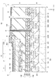
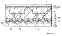
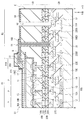
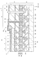
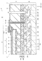
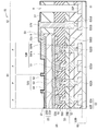
- FIG. 3 is a schematic cross-sectional view illustrating an example of the configuration of the light receiving element according to the first embodiment of the present disclosure. It is a plane schematic diagram showing the schematic structure of the whole light receiving element shown in FIG.
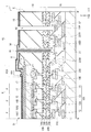
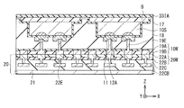
- FIG. 7 is a schematic cross-sectional view illustrating another example of the configuration of the light receiving element according to the first embodiment of the present disclosure.
- FIG. 6 is a schematic cross-sectional view showing another configuration example of the configuration of the light receiving element shown in FIG. 3.
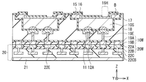
- FIG. 7 is a schematic cross-sectional view illustrating another example of the configuration of the light receiving element according to the first embodiment of the present disclosure.
- FIG. 7 is a schematic cross-sectional view illustrating another example of the configuration of the light receiving element according to the first embodiment of the present disclosure.
- FIG. 7 is a schematic cross-sectional view illustrating another example of the configuration of the light receiving element according to the first embodiment of the present disclosure.
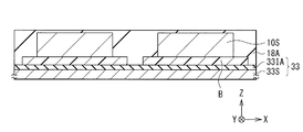
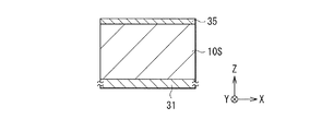
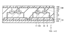
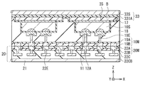
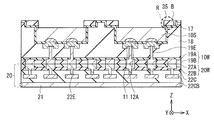
- FIG. 9 is a schematic cross sectional view for illustrating one step in the method for manufacturing the light receiving element shown in FIG. 1. It is a cross-sectional schematic diagram showing the process of following FIG. 7A. It is a cross-sectional schematic diagram showing the process of following FIG. 7B. It is a plane schematic diagram showing an example of the process of FIG. 7C.
- FIG. 9 is a schematic plan view showing another example (1) of the configuration of the semiconductor layer shown in FIG. 8.
- FIG. 9 is a schematic plan view showing another example (2) of the configuration of the semiconductor layer shown in FIG. 8.
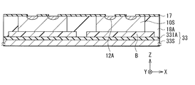
- FIG. 10B is a schematic diagram showing a cross-sectional configuration along the line BB shown in FIG. 10A. It is a cross-sectional schematic diagram showing the process of following FIG. 7C.
- FIG. 11B is a schematic diagram illustrating an example of a planar configuration of the process illustrated in FIG. 11A.
- FIG. 12D is a schematic diagram illustrating an example of a planar configuration of the process illustrated in FIG. 11B.
- FIG. 11B is a schematic diagram illustrating another example (1) of the planar configuration of the step illustrated in FIG. 11A.
- FIG. 12C is a schematic diagram illustrating another example (1) of the planar configuration of the step illustrated in FIG. 11B.
- FIG. 11B is a schematic diagram illustrating another example (2) of the planar configuration of the process illustrated in FIG. 11A.
- FIG. 12C is a schematic diagram illustrating another example (2) of the planar configuration of the step illustrated in FIG.
- FIG. 12C is a schematic sectional view showing another example (1) of the step shown in FIG. 11B.
- FIG. 12C is a schematic sectional view showing another example (2) of the step shown in FIG. 11B.
- It is a cross-sectional schematic diagram showing the process of following FIG. 11B.
- It is a cross-sectional schematic diagram showing the process of following FIG. 17A.
- It is a cross-sectional schematic diagram showing the process of following FIG. 17B.
- It is a cross-sectional schematic diagram showing the process of following FIG. 17F.
- FIG. 17G It is a cross-sectional schematic diagram showing the process of following FIG. 17G. It is a cross-sectional schematic diagram showing the process of following FIG. 17H. It is a cross-sectional schematic diagram showing the process of following FIG. 17I. It is a cross-sectional schematic diagram showing the structure of the light receiving element which concerns on the 2nd Embodiment of this indication. It is a characteristic view showing the relationship between the wavelength and the transmittance in each metal. It is a characteristic view showing the relationship between the wavelength and reflectance in various conductive films. It is a characteristic view showing the relationship between the film thickness of various conductive films and the amount of warpage of a Si substrate.
- FIG. 11 is a schematic cross-sectional view illustrating another example of the configuration of the light receiving element according to Modification Example 1 of the present disclosure.
- FIG. 27 is a schematic cross-sectional view for explaining a step of the method for manufacturing the light-receiving element shown in FIG. 26. It is a cross-sectional schematic diagram showing the process of following FIG. 27A.
- FIG. 28C is a schematic sectional view showing another example (1) of the step shown in FIG. 27B. It is a cross-sectional schematic diagram showing the other example (2) of the process shown in FIG. 27B. It is a cross-sectional schematic diagram showing the process of following FIG. 27B. It is a cross-sectional schematic diagram showing the process of following FIG. 30A.
- FIG. 10 is a schematic cross-sectional view illustrating a schematic configuration of a light receiving element according to Modification 2 of the present disclosure.
- FIG. 10 is a schematic cross-sectional view illustrating a schematic configuration of a light receiving element according to Modification 2 of the present disclosure.
- FIG. 13 is a schematic cross-sectional view for explaining a step of the method for manufacturing the light-receiving element according to Modification 3 of the present disclosure. It is a cross-sectional schematic diagram showing the process of following FIG. 32A.
- FIG. 33 is a cross-sectional schematic diagram showing a process following on the process shown in FIG. 32B.
- FIG. 33 is a schematic cross-sectional view showing a process following on the process shown in FIG. 32C.
- FIG. 33 is a schematic cross-sectional view showing a configuration of a main part of a light-receiving element completed through the steps following FIG. 32E.
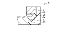
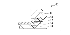
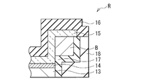
- FIG. 32E It is a cross-sectional schematic diagram (1) which expands and shows a part shown to FIG. 32E. It is a cross-sectional schematic diagram (1) which expands and represents a part shown in FIG. FIG. 34B is a schematic sectional view illustrating another example of the shape of the opening illustrated in FIG. 34A. It is a cross-sectional schematic diagram (2) which expands and shows a part shown to FIG. 32E. It is a cross-sectional schematic diagram (2) which expands and shows a part shown in FIG. FIG. 35B is a schematic sectional view illustrating another example of the shape of the opening illustrated in FIG. 35A. It is a cross-sectional schematic diagram (3) which expands and represents a part shown to FIG. 32E. FIG.
- FIG. 34 is a schematic cross-sectional view (3) illustrating a part of FIG. 33 in an enlarged manner.
- FIG. 36B is a schematic sectional view showing another example of the shape of the opening shown in FIG. 36A. It is a cross-sectional schematic diagram (4) which expands and shows a part shown to FIG. 32E.
- FIG. 13 is a schematic cross-sectional view illustrating an example of the configuration of a light receiving element according to Modification 4 of the present disclosure.
- FIG. 16 is a schematic cross-sectional view illustrating another example of the configuration of the light receiving element according to Modification 4 of the present disclosure.
- FIG. 16 is a schematic cross-sectional view illustrating an example of the configuration of a light receiving element according to Modification 5 of the present disclosure.
- First embodiment (example of light-receiving element having non-reducing layer on second electrode) 1-1. Configuration of light receiving element 1-2. Manufacturing method of light receiving element 1-3. Operation of light receiving element 1-4. Actions and effects 2.
- Second embodiment (example in which a conductive film is formed using a conductive material containing Al) 3.
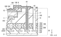
- FIG. 1 schematically illustrates an example of a cross-sectional configuration of a semiconductor element (light receiving element 1) according to the first embodiment of the present disclosure.
- FIG. 2 schematically shows the overall planar configuration of the light receiving element 1 shown in FIG. Note that FIG. 1 shows a cross-sectional configuration taken along the line II shown in FIG.
- the light receiving element 1 is applied to, for example, an infrared sensor using a compound semiconductor material such as a III-V semiconductor, and is, for example, a visible region (for example, 380 nm or more and less than 780 nm) to a short infrared region (for example, 780 nm or more).
- Light having a wavelength of less than 2400 nm has a photoelectric conversion function.
- the light receiving element 1 is provided with a plurality of light receiving unit regions (pixels P) arranged two-dimensionally, for example.
- FIG. 1 shows a sectional configuration of a portion corresponding to three pixels P.
- the light receiving element 1 has a central element region R1 and a peripheral region R2 provided outside the element region R1 and surrounding the element region R1.
- the light receiving element 1 has a conductive film 15B provided from the element region R1 to the peripheral region R2.
- the conductive film 15B has an opening in a region facing the central portion of the element region R1.
- the light receiving element 1 has a laminated structure of an element substrate 10 and a read circuit substrate 20, as shown in FIG.
- One surface of the element substrate 10 is a light incident surface (light incident surface S1), and the surface opposite to the light incident surface S1 (the other surface) is a joint surface (joint surface S2) with the read circuit board 20. ..
- the element substrate 10 has a wiring layer 10W, a first electrode 11, a semiconductor layer 10S (first semiconductor layer), a second electrode 15, and passivation films 16A and 16B in this order from a position close to the read circuit substrate 20. There is.
- the surface of the semiconductor layer 10S facing the wiring layer 10W and the end surface (side surface) are covered with an insulating film 17.
- the readout circuit board 20 is a so-called ROIC (Readout integrated circuit), and includes the wiring layer 20W and the multilayer wiring layer 22C that are in contact with the bonding surface S2 of the element substrate 10, and the wiring layer 20W and the multilayer wiring layer 22C in between.
- the element substrate 10 has a semiconductor layer 10S in the element region R1.
- the region where the semiconductor layer 10S is provided is the element region R1 of the light receiving element 1.
- a region of the element region R1 exposed from the conductive film 15B (a region facing the opening of the conductive film 15B) is a light receiving region.
- a region of the element region R1 that is covered with the conductive film 15B near the peripheral region R2 is an OPB (Optical Black) region R1B.
- the OPB region R1B is provided so as to surround the light receiving region.
- the OPB region R1B is used to obtain a black level pixel signal.
- the element substrate 10 has a buried layer 18 together with the insulating film 17 in the peripheral region R2.
- the wiring layer 10W is provided over the element region R1 and the peripheral region R2, and has a joint surface S2 with the read circuit board 20.
- the joint surface S2 of the element substrate 10 is provided in the element region R1 and the peripheral region R2.
- the joint surface S2 of the element region R1 and the joint surface S2 of the peripheral region R2 form the same plane. There is. As will be described later, in the light receiving element 1, by providing the buried layer 18, the bonding surface S2 of the peripheral region R2 is formed.
- the wiring layer 10W has a contact electrode 19E and a dummy electrode 19ED in, for example, the interlayer insulating films 19A and 19B.
- the inter-layer insulating film 19B is arranged on the side of the read circuit substrate 20, the inter-layer insulating film 19A is arranged on the side of the first contact layer 12, and the inter-layer insulating films 19A and 19B are laminated.
- the interlayer insulating films 19A and 19B are made of, for example, an inorganic insulating material. Examples of the inorganic insulating material include silicon nitride (SiN), aluminum oxide (Al 2 O 3 ), silicon oxide (SiO 2 ) and hafnium oxide (HfO 2 ).
- the interlayer insulating films 19A and 19B may be made of the same inorganic insulating material.
- the contact electrode 19E is provided in the element region R1, for example.
- the contact electrode 19E is for electrically connecting the first electrode 11 and the readout circuit substrate 20 and is provided in the element region R1 for each pixel P.
- Adjacent contact electrodes 19E are electrically separated by the buried layer 18 and the interlayer insulating films 19A and 19B.
- the contact electrode 19E is made of, for example, a copper (Cu) pad and is exposed on the joint surface S2.
- the dummy electrode 19ED is provided in the peripheral region R2, for example.
- the dummy electrode 19ED is connected to the dummy electrode 22ED of the wiring layer 20W described later. By providing the dummy electrode 19ED and the dummy electrode 22ED, the strength of the peripheral region R2 can be improved.
- the dummy electrode 19ED is formed in the same process as the contact electrode 19E, for example.
- the dummy electrode 19ED is composed of, for example, a copper (Cu) pad and is exposed on the bonding surface S2.
- the first electrode 11 provided between the contact electrode 19E and the semiconductor layer 10S has signal charges generated in the photoelectric conversion layer 13 (holes or electrons; hereinafter, for convenience, the signal charge is described as holes).
- the first electrode 11 is provided so as to fill the opening of the insulating film 17 and is in contact with the semiconductor layer 10S (more specifically, a diffusion region 12A described later).
- the first electrode 11 is, for example, larger than the opening of the insulating film 17, and a part of the first electrode 11 is provided in the buried layer 18.
- the upper surface of the first electrode 11 (the surface on the semiconductor layer 10S side) is in contact with the diffusion region 12A, and the lower surface and part of the side surface of the first electrode 11 are in contact with the buried layer 18.
- the adjacent first electrodes 11 are electrically separated by the insulating film 17 and the buried layer 18.
- the first electrode 11 is, for example, titanium (Ti), tungsten (W), titanium nitride (TiN), platinum (Pt), gold (Au), germanium (Ge), palladium (Pd), zinc (Zn), nickel. (Ni) and aluminum (Al), or an alloy containing at least one of them.
- the first electrode 11 may be a single film of such a constituent material or a laminated film in which two or more kinds are combined.
- the first electrode 11 is composed of a laminated film of titanium and tungsten.
- the thickness of the first electrode 11 is, for example, several tens nm to several hundreds nm.
- the semiconductor layer 10S includes, for example, a first contact layer 12, a photoelectric conversion layer 13, and a second contact layer 14 from a position close to the wiring layer 10W.
- the first contact layer 12, the photoelectric conversion layer 13, and the second contact layer 14 have the same planar shape as each other, and their end faces are arranged at the same position in plan view.
- the first contact layer 12 is provided, for example, in common to all the pixels P and is arranged between the insulating film 17 and the photoelectric conversion layer 13.
- the first contact layer 12 is for electrically separating adjacent pixels P, and the first contact layer 12 is provided with, for example, a plurality of diffusion regions 12A.
- a compound semiconductor material having a bandgap larger than that of the compound semiconductor material forming the photoelectric conversion layer 13 for the first contact layer 12 it is possible to suppress dark current.
- n-type InP indium phosphide
- the diffusion regions 12A provided in the first contact layer 12 are arranged apart from each other.
- the diffusion region 12A is arranged for each pixel P, and the first electrode 11 is connected to each diffusion region 12A.
- the diffusion region 12A is also provided in the OPB region R1B.
- the diffusion region 12A is for reading out the signal charges generated in the photoelectric conversion layer 13 for each pixel P, and contains, for example, a p-type impurity. Examples of p-type impurities include Zn (zinc). In this way, the pn junction interface is formed between the diffusion region 12A and the first contact layer 12 other than the diffusion region 12A, and the adjacent pixels P are electrically separated.
- the diffusion region 12A is provided, for example, in the thickness direction of the first contact layer 12 and is also provided in a part of the photoelectric conversion layer 13 in the thickness direction.
- the photoelectric conversion layer 13 between the first electrode 11 and the second electrode 15, more specifically, between the first contact layer 12 and the second contact layer 14, is common to all pixels P, for example. It is provided.
- the photoelectric conversion layer 13 absorbs light having a predetermined wavelength to generate signal charges, and is made of, for example, a compound semiconductor material such as an i-type III-V group semiconductor. Examples of the compound semiconductor material forming the photoelectric conversion layer 13 include InGaAs (indium gallium arsenide), InAsSb (indium arsenide antimony), InAs (indium arsenide), InSb (indium antimony), and HgCdTe (mercury cadmium tellurium). Can be mentioned.
- the photoelectric conversion layer 13 may be made of Ge (germanium). In the photoelectric conversion layer 13, for example, light having a wavelength in the visible region to the short infrared region is photoelectrically converted.
- the second contact layer 14 is provided in common to all the pixels P, for example.
- the second contact layer 14 is provided between the photoelectric conversion layer 13 and the second electrode 15 and is in contact with them.
- the second contact layer 14 is a region in which charges discharged from the second electrode 15 move, and is made of, for example, a compound semiconductor containing n-type impurities.
- n-type InP indium phosphide
- the second electrode 15 is provided, for example, as an electrode common to each pixel P on the second contact layer 14 (on the light incident side) so as to be in contact with the second contact layer 14.
- the second electrode 15 is for discharging, of the charges generated in the photoelectric conversion layer 13, charges that are not used as signal charges (cathode). For example, when holes are read out from the first electrode 11 as signal charges, for example, electrons can be discharged through the second electrode 15.
- the second electrode 15 is formed of a conductive film that can transmit incident light such as infrared rays.
- ITO Indium Tin Oxide
- ITiO In 2 O 3 —TiO 2
- the second electrode 15 may be provided in a grid shape so as to partition adjacent pixels P, as in Modification 4 described later. In that case, the second electrode 15 can be made of a conductive material having low light transmittance.
- the passivation films 16A and 16B cover the second electrode 15 from the light incident surface S1 side.
- the passivation films 16A and 16B are preferably formed using a material that does not absorb light having a wavelength in the visible region (for example, 380 nm or more and less than 780 nm) to the short infrared region (for example, 780 nm or more and less than 2400 nm).
- the passivation films 16A and 16B may be formed by using the same material or different materials. Further, the passivation films 16A and 16B may have an antireflection function.
- the passivation films 16A and 16B can be formed by, for example, an ALD (Atomic Layer Deposition) method, a CVD (Chemical Vapor Deposition) method, a PVD (Physical Vapor Deposition) method, or a coating method.
- ALD Atomic Layer Deposition
- CVD Chemical Vapor Deposition
- PVD Physical Vapor Deposition
- the passivation film 16A is provided on the second electrode 15 as described above, and extends to the chip end E of the peripheral region R2, for example.
- the passivation film 16A has an opening 16H in the OPB region R1B. As shown in FIG. 2, the opening 16H is provided, for example, in a frame shape surrounding the light receiving area.
- the opening 16H may be, for example, a square or circular hole in a plan view.
- a conductive film 15B described later is electrically connected to the second electrode 15 through the opening 16H of the passivation film 16A.
- the passivation film 16A is preferably formed using a non-reducing material.
- a non-reducing material for example, an oxide (M x O y), a nitride (M x N y) and oxynitrides (M x O y N z) and the like.
- M include silicon (Si), titanium (Ti), hafnium (Hf), zirconium (Zr) and yttrium (Y).
- x, y, and z are integers of 1 or more.
- silicon nitride (SiN) it is desirable to use a film forming method that does not use a reducing gas. Examples of such a film forming method include a sputtering method and a coating method.
- the passivation film 16A may be formed as, for example, a single layer film made of any of the above materials.
- the single layer film preferably has a film density of 2.0 g/cm 3 or more.
- the upper limit of the film density is not particularly limited, but is, for example, 8.0 g/cm 3 or less.
- the film density is defined by mass of thin film/volume (g/cm 3 ) and is determined by, for example, XRR measurement.
- a sealing function is added to the passivation film 16A.
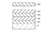
- the passivation film 16A may be formed as, for example, a laminated film in which the film 16A1 and the film 16A2 as shown in FIG.
- the passivation film 16A is a laminated film
- the film 16A1 that is in direct contact with the second electrode 15 is preferably formed using any of the above materials.
- the thickness of the film 16A1 is, for example, 0.5 nm or more.
- the film 16A2 it is preferable to use a material having a high sealing property such as silicon nitride (SiN) or aluminum oxide (Al 2 O 3 ).
- the passivation film 16A may be a multilayer film in which three or more films 16A1, 16A2, 16A3, 16A4... 16AX are laminated on the second electrode 15.
- the passivation film 16B is provided so as to cover the passivation film 16A and the conductive film 15B, and, for example, extends to the chip end E of the peripheral region R2 similarly to the passivation film 16A.
- silicon nitride (SiN), aluminum oxide (Al 2 O 3 ), silicon oxide (SiO 2 ) and tantalum oxide (Ta 2 O 3 ) can be used.
- the film formation method of silicon nitride (SiN) is not particularly limited, and in addition to the sputtering method and the coating method, the silicon nitride (SiN) film formed by the plasma CVD method using a reducing gas is used. May be used.
- the insulating film 17 is provided between the first contact layer 12 and the burying layer 18, and is an end surface of the first contact layer 12, an end surface of the photoelectric conversion layer 13, an end surface of the second contact layer 14, and the second electrode 15. Of the passivation film 16 in the peripheral region R2.
- the insulating film 17 is configured to include an oxide such as silicon oxide (SiO x ) or aluminum oxide (Al 2 O 3 ).
- the insulating film 17 may be configured by a laminated structure including a plurality of films.
- the insulating film 17 may be made of a silicon (Si)-based insulating material such as silicon oxynitride (SiON), carbon-containing silicon oxide (SiOC), silicon nitride (SiN), and silicon carbide (SiC).
- Si silicon
- SiON silicon oxynitride
- SiOC carbon-containing silicon oxide
- SiN silicon nitride
- SiC silicon carbide
- the insulating film 17 has a thickness of, for example, several tens nm to several hundreds nm.
- the conductive film 15B is provided from the OPB region R1B to the through hole H1 in the peripheral region R2.
- the conductive film 15B is in contact with the second electrode 15 at the opening 16H of the passivation film 16A provided in the OPB region R1B and is also in contact with the wiring (wiring 22CB described later) of the read circuit board 20 through the through hole H1. ..
- a voltage is supplied from the read circuit board 20 to the second electrode 15 via the conductive film 15B.
- the conductive film 15B functions as a voltage supply path to the second electrode 15 and also functions as a light shielding film, and forms the OPB region R1B.
- the conductive film 15B is made of a metal material containing, for example, tungsten (W), aluminum (Al), titanium (Ti), molybdenum (Mo), tantalum (Ta) or copper (Cu).
- the passivation film 16B may be provided on the conductive film 15B.
- the adhesive layer B may be provided between the end of the second contact layer 14 and the second electrode 15.
- the adhesive layer B is used when the light receiving element 1 is formed, as will be described later, and has a role of bonding the semiconductor layer 10S to a temporary substrate (temporary substrate 33 of FIG. 7C described later).
- the adhesive layer B is made of, for example, tetraethoxysilane (TEOS) or silicon oxide (SiO 2 ).
- TEOS tetraethoxysilane
- SiO 2 silicon oxide
- the adhesive layer B is, for example, provided so as to be wider than the end surface of the semiconductor layer 10S, and is covered with the embedded layer 18 together with the semiconductor layer 10S.
- An insulating film 17 is provided between the adhesive layer B and the embedded layer 18.
- the adhesive layer B may be provided over a wide region of the peripheral region R2, and for example, extends from the vicinity of the edge of the semiconductor layer 10S (element region R1) to between the through holes H1 and H2. Good ( Figure 5). Alternatively, the adhesive layer B may extend from the vicinity of the edge of the semiconductor layer 10S (element region R1) to the chip end (chip end E) (FIG. 6).
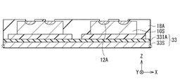
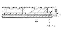
- the embedded layer 18 is for filling the step between the temporary substrate (the temporary substrate 33 of FIG. 7C described later) and the semiconductor layer 10S in the manufacturing process of the light receiving element 1. Although the details will be described later, by forming the buried layer 18, occurrence of defects in the manufacturing process due to the step between the semiconductor layer 10S and the temporary substrate 33 can be suppressed.
- the buried layer 18 in the peripheral region R2 is provided between the wiring layer 10W and the insulating film 17 and between the wiring layer 10W and the passivation film 16, and has a thickness equal to or larger than the thickness of the semiconductor layer 10S, for example. There is.
- the buried layer 18 is provided so as to surround the semiconductor layer 10S, a region (peripheral region R2) around the semiconductor layer 10S is formed.
- a bonding surface S2 with the read circuit board 20 can be provided in the peripheral region R2. If the bonding surface S2 is formed in the peripheral region R2, the thickness of the buried layer 18 may be reduced, but the buried layer 18 covers the semiconductor layer 10S in the thickness direction, and the entire end surface of the semiconductor layer 10S is buried.
- the embedded layer 18 covers the entire end surface of the semiconductor layer 10S with the insulating film 17 interposed therebetween, it is possible to effectively suppress the intrusion of moisture into the semiconductor layer 10S.
- the buried layer 18 in the element region R1 is provided between the semiconductor layer 10S and the wiring layer 10W so as to cover the first electrode 11.
- the surface of the buried layer 18 on the bonding surface S2 side is flattened, and the wiring layer 10W is provided on the surface of the flattened buried layer 18 in the peripheral region R2.
- an inorganic insulating material such as silicon oxide (SiO x ), silicon nitride (SiN), silicon oxynitride (SiON), carbon-containing silicon oxide (SiOC), and silicon carbide (SiC) is used.
- the wiring layer 10W including the interlayer insulating films 19A and 19B and the contact electrode 19E is formed above the buried layer 18. (FIG. 17D described later).
- the read circuit board 20 including the wiring layer 20W is bonded to the element substrate 10 including the wiring layer 10W (FIG. 17E described later) to form the light receiving element 1.
- the contact electrode 19E of the wiring layer 10W and the contact electrode 22E of the wiring layer 20W are connected.
- the contact electrodes 19E and 22E have, for example, Cu pads, and the contact electrodes 19E and 22E are connected by direct bonding of the Cu pads.
- the buried layer 18 disposed below the copper film to be polished is required to have a hardness that can withstand the stress during polishing. Further, in order to directly bond the Cu pads of the contact electrodes 19E and 22E to each other, it is necessary to form the element substrate 10 and the read circuit substrate 20 to be extremely flat. Therefore, it is preferable that the buried layer 18 arranged below the copper film has a hardness that can withstand the stress during polishing.
- the constituent material of the buried layer 18 is preferably a material having a higher hardness than the encapsulant or the organic material arranged around the die in a general semiconductor package.
- the embedded layer 18 can be formed by depositing this inorganic insulating material by, for example, a CVD (Chemical Vapor Deposition) method, a sputtering method, or a coating method.
- CVD Chemical Vapor Deposition
- the buried layer 18 is provided with through holes H1 and H2 penetrating the buried layer 18.
- the through holes H1 and H2 penetrate the wiring layer 10W together with the buried layer 18 and reach the read circuit board 20.
- the through holes H1 and H2 have, for example, a quadrangular planar shape, and a plurality of through holes H1 and H2 are provided so as to surround the element region R1 (FIG. 1A).
- the through hole H1 is provided closer to the element region R1 than the through hole H2, and the sidewall and bottom surface of the through hole H1 are covered with the conductive film 15B.
- the through hole H1 is for connecting the second electrode 15 (conductive film 15B) and the wiring of the read circuit board 20 (wiring 22CB described later), and the passivation film 16, the embedding layer 18, and the wiring layer 10W. Is provided to penetrate.
- the through hole H2 is provided closer to the chip end E than the through hole H1, for example.
- the through hole H2 penetrates the passivation film 16, the buried layer 18, and the wiring layer 10W and reaches a pad electrode (a pad electrode 22P described later) of the read circuit board 20.
- the outside and the light receiving element 1 are electrically connected to each other through the through hole H2.
- the through holes H1 and H2 may not reach the read circuit board 20.
- the through holes H1 and H2 may reach the wiring of the wiring layer 10W, and this wiring may be connected to the wiring 22CB and the pad electrode 22P of the read circuit board 20.
- the through holes H1 and H2 may penetrate the adhesive layer B (FIGS. 5 and 6).
- the distance between the first electrode 11 and the second electrode 15 be a distance sufficient for photoelectric conversion and not too far apart. That is, it is preferable to reduce the thickness of the element substrate 10.
- the distance between the first electrode 11 and the second electrode 15 or the thickness of the element substrate 10 is 10 ⁇ m or less, further 7 ⁇ m or less, and further 5 ⁇ m or less.
- the semiconductor substrate 21 of the read circuit board 20 faces the element substrate 10 with the wiring layer 20W and the multilayer wiring layer 22C in between.
- the semiconductor substrate 21 is made of, for example, silicon (Si).
- a plurality of transistors are provided near the surface of the semiconductor substrate 21 (the surface on the wiring layer 20W side).
- a read circuit Read Out Circuit
- the wiring layer 20W has, for example, an interlayer insulating film 22A and an interlayer insulating film 22B in this order from the element substrate 10 side, and these interlayer insulating films 22A and 22B are provided in a laminated manner.
- the contact electrode 22E and the dummy electrode 22ED are provided in the interlayer insulating film 22A.
- the multilayer wiring layer 22C is provided to face the element substrate 10 with the wiring layer 20W in between.
- a pad electrode 22P and a plurality of wirings 22CB are provided in this multilayer wiring layer 22C.
- the interlayer insulating films 22A and 22B are made of, for example, an inorganic insulating material. Examples of the inorganic insulating material include silicon nitride (SiN), aluminum oxide (Al 2 O 3 ), silicon oxide (SiO 2 ) and hafnium oxide (HfO 2 ).
- the contact electrode 22E is for electrically connecting the first electrode 11 and the wiring 22CB, and is provided for each pixel P in the element region R1.
- the contact electrode 22E is in contact with the contact electrode 19E at the joint surface S2 of the element substrate 10.
- the adjacent contact electrodes 22E are electrically separated by the interlayer insulating film 22A.
- the dummy electrode 22ED provided in the peripheral region R2 is in contact with the dummy electrode 19ED at the bonding surface S2 of the element substrate 10.
- the dummy electrode 22ED is formed in the same process as the contact electrode 22E, for example.
- the contact electrode 22E and the dummy electrode 22ED are made of, for example, copper (Cu) pads, and are exposed on the surface of the read circuit board 20 facing the element substrate 10. That is, for example, CuCu bonding is performed between the contact electrode 19E and the contact electrode 22E and between the dummy electrode 19ED and the dummy electrode 22ED.
- the wiring 22CB connected to the contact electrode 19E is connected to the transistor provided in the vicinity of the surface of the semiconductor substrate 21, and the first electrode 11 and the readout circuit are connected to each pixel P. ..
- the wiring 22CB connected to the conductive film 15B via the through hole H1 is connected to, for example, a predetermined potential.
- one of the charges (for example, holes) generated in the photoelectric conversion layer 13 is read from the first electrode 11 to the readout circuit via the contact electrodes 19E and 22E, and is generated in the photoelectric conversion layer 13.
- the other of the charges (for example, electrons) is discharged from the second electrode 15 to a predetermined potential via the conductive film 15B.
- the pad electrode 22P provided in the peripheral region R2 is for electrical connection with the outside.
- a through hole H2 penetrating the element substrate 10 and reaching the pad electrode 22P is provided in the vicinity of the chip end E of the light receiving element 1, and an electrical connection with the outside is made through the through hole H2.
- the connection is made, for example, by a method such as wire bond or bump. For example, even if a predetermined potential is supplied from the external terminal arranged in the through hole H2 to the second electrode 15 via the wiring 22CB of the through hole H2 read circuit board 20 and the conductive film 15B. Good.
- the signal voltage read from the first electrode 11 is read to the read circuit of the semiconductor substrate 21 via the contact electrodes 19E and 22E, and passes through this read circuit.
- the output may be output to an external terminal arranged in the through hole H2.
- the signal voltage may be output to an external terminal together with the read circuit, for example, via another circuit included in the read circuit board 20.
- the other circuits are, for example, a signal processing circuit and an output circuit.
- the thickness of the read circuit board 20 is preferably larger than the thickness of the element board 10.
- the thickness of the read circuit board 20 is preferably twice or more, more preferably 5 times or more, and further preferably 10 times or more than the thickness of the element substrate 10.
- the thickness of the readout circuit board 20 is, for example, 100 ⁇ m or more, 150 ⁇ m or more, or 200 ⁇ m or more.
- the read circuit board 20 having such a large thickness ensures the mechanical strength of the light receiving element 1.
- the readout circuit board 20 may include only one layer of the semiconductor substrate 21 forming the circuit, or may further include a substrate such as a support substrate in addition to the semiconductor substrate 21 forming the circuit. Good.
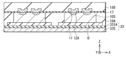
- the light receiving element 1 can be manufactured, for example, as follows. 7A to 17J show the manufacturing process of the light receiving element 1 in process order.
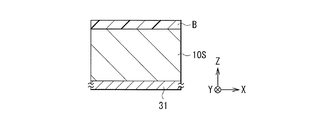
- the semiconductor layer 10S is epitaxially grown on the growth substrate 31 made of InP, for example.
- the growth substrate 31 has a thickness of, for example, several hundred ⁇ m, and the semiconductor layer 10S has a thickness of, for example, several ⁇ m.
- the adhesive layer B is formed on the semiconductor layer 10S.
- the diameter of the growth substrate 31 is, for example, 6 inches or less.
- the semiconductor layer 10S is formed by, for example, epitaxially growing n-type InP forming the first contact layer 12, i-type InGaAs forming the photoelectric conversion layer 13, and n-type InP forming the second contact layer 14 in this order. Let me do it.
- the semiconductor layer 10S may be formed after forming the buffer layer and the stopper layer on the growth substrate 31, for example.
- the temporary substrate 33 has, for example, an insulating layer (insulating layer 33IA) and a substrate 33S.
- the insulating layer 33IA is arranged, for example, between the adhesive layer B and the substrate 33S.
- the temporary substrate 33 has a diameter larger than that of the growth substrate 31, and the substrate 33S is, for example, a silicon (Si) substrate.
- the diameter of the temporary substrate 33 is, for example, 8 inches to 12 inches.
- the small-diameter growth substrate 31 By bonding the small-diameter growth substrate 31 to the large-diameter temporary substrate 33, it becomes possible to use various devices for a large-diameter substrate when forming the element substrate 10.
- the readout circuit board 20 and the element substrate 10 can be bonded to each other by CuCu, and the pixel P can be miniaturized.
- the growth substrate 31 may be bonded to the temporary substrate 33 by plasma activation bonding, room temperature bonding, bonding using an adhesive (adhesive bonding), or the like. In this way, for example, the wafer-shaped semiconductor layer 10S is bonded to the temporary substrate 33.
- the thickness of the temporary substrate 33 is, for example, several hundreds ⁇ m.
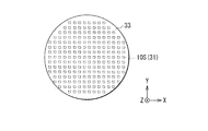
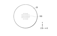
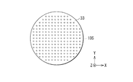
- FIG. 8 and 9 show an example of a planar configuration of the temporary substrate 33 and the semiconductor layer 10S (growth substrate 31).
- the semiconductor layer 10S in a wafer state smaller than the temporary substrate 33 may be bonded to the temporary substrate 33 in a wafer state (FIG. 8), and the semiconductor layer 10S in a chip state may be separated from the temporary substrate 33 in a wafer state. You may make it join several in the state (FIG. 9).
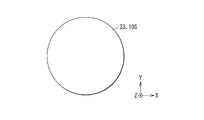
- the semiconductor substrate 10S in the wafer state having the same size as the temporary substrate 33 may be bonded to the temporary substrate 33 in the wafer state.
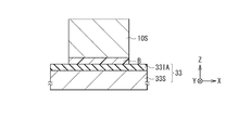
- 10A shows a planar configuration of the temporary substrate 33 and the semiconductor layer 10S (growth substrate 31), and
- FIG. 10B shows a sectional configuration taken along the line BB of FIG. 10A.
- the growth substrate 31 having the semiconductor layer 10S formed thereon is bonded to the temporary substrate 33, the growth substrate 31 is removed as shown in FIG. 11A.
- the growth substrate 31 can be removed by mechanical grinding, CMP (Chemical Mechanical Polishing), wet etching, dry etching, or the like. At this time, the growth substrate 31 may partially remain. Further, the semiconductor layer 10S may be partially etched.
- FIG. 11B for example, the semiconductor layer 10S is etched to a predetermined size in accordance with the mark on the temporary substrate 33. As a result, a plurality of semiconductor layers 10S in a chip state are formed.
- FIG. 11B and subsequent figures show two semiconductor layers 10S among the plurality of semiconductor layers 10S in a chip state.
- FIG. 12A shows an example of a planar configuration of the semiconductor layer 10S before molding
- FIG. 12B shows an example of a planar configuration of the semiconductor layer 10S after molding following FIG. 12A
- 13A shows another example of the planar configuration of the semiconductor layer 10S before molding
- FIG. 13B shows another example of the planar configuration of the semiconductor layer 10S after molding following FIG. 13A.
- a plurality of semiconductor layers 10S in a chip state may be molded into a plurality of semiconductor layers 10S in a smaller chip state.
- the adhesive layer B is etched together with the semiconductor layer 10S, for example.
- the adhesive layer B may remain wider than the semiconductor layer 10S, and the adhesive layer B may spread around the semiconductor layer 10S (FIG. 11B).
- the adhesive layer B may be narrower than the semiconductor layer 10S, and a void may be formed between the semiconductor layer 10S and the temporary substrate 33.
- the adhesive layer B may be etched to the same size as the semiconductor layer 10S.
- the adhesive layer B may not be etched when the semiconductor layer 10S is etched.
- a diffusion region 12A is formed in the semiconductor layer 10S for each pixel P. Thereby, element isolation is performed.
- the insulating film 17 is used as a hard mask. Specifically, after forming the insulating film 17 so as to cover the upper surface (the surface opposite to the bonding surface with the temporary substrate 33) and the side surface of the semiconductor layer 10S, the insulating film 17 that covers the upper surface of the semiconductor layer 10S is etched. To form an opening. After that, vapor phase diffusion of p-type impurities is performed using the insulating film 17 as a hard mask. As a result, the diffusion region 12A is formed in the selective region.
- the diffusion depth is, for example, several hundreds nm, and the diffusion is substantially isotropic.
- the diffusion region 12A may be formed by ion implantation or the like using a resist mask.
- the diffusion region 12A is formed in the semiconductor layer 10S provided on the large-diameter temporary substrate 33, the pixel P can be miniaturized.
- the first electrode 11 is formed on the semiconductor layer 10S as shown in FIG. 17B.
- a titanium (Ti)/tungsten (W) laminated film is formed in the opening provided in the insulating film 17 by a CVD method, a PVD method, an ALD method, an evaporation method, or the like, and then the laminated film is formed.
- the film is formed by patterning using photolithography and etching.
- the embedded layer 18 is formed on the entire surface of the temporary substrate 33.
- the buried layer 18 is formed by, for example, depositing an insulating material on the entire surface of the temporary substrate 33 so as to fill the semiconductor layer 10S, and then planarizing the film by CMP (Chemical Mechanical Polishing). Thereby, the buried layer 18 that covers the periphery of the semiconductor layer 10S (peripheral region R2) and the upper surface of the semiconductor layer 10S (the surface farthest from the temporary substrate 33) is formed.
- CMP Chemical Mechanical Polishing
- the wiring layer 10W facing the semiconductor layer 10S is formed with the embedded layer 18 in between.
- the interlayer insulating film 19A and the interlayer insulating film 19B on the buried layer 18 in this order, an opening is formed in a region of the interlayer insulating films 19A and 19B facing the first electrode 11.
- a copper (Cu) film in the openings of the interlayer insulating films 19A and 19B by a vapor deposition method, a PVD method, a plating method, or the like, the surface of the copper film is polished by, for example, the CMP method, so that the contact electrode 19E. To form.
- the dummy electrode 19ED is formed in the peripheral region R2 in the same step as the step of forming the contact electrode 19E.
- the wiring layer 10W is formed on the large-diameter temporary substrate 33, various devices for a large-diameter substrate can be used.
- the readout circuit board 20 is attached to the temporary substrate 33 with the wiring layer 10W in between. At this time, the wiring layer 20W is formed on the read circuit board 20 in advance.
- the wiring layer 20W of the read circuit board 20 has a contact electrode 22E and a dummy electrode 22ED.
- the contact electrode 22E and the dummy electrode of the wiring layer 20W are used.
- the 22ED and the contact electrode 19E and the dummy electrode 19ED of the wiring layer 10W are CuCu-bonded.
- a junction surface S2 in which the contact electrode 19E and the contact electrode 22E are joined is formed in the element region R1
- a junction surface S2 in which the dummy electrode 19ED and the dummy electrode 22ED are joined is formed in the peripheral region R2. It is formed.
- the peripheral region R2 of the element substrate 10 is also joined to the read circuit substrate 20.
- the temporary board 33 is removed as shown in FIG. 17F.
- the temporary substrate 33 can be removed by using, for example, mechanical grinding, wet etching, dry etching, or the like.
- the adhesive layer B and the like are also removed to expose the surface of the semiconductor layer 10S. At this time, unnecessary layers of the semiconductor layer 10S may be removed. Further, the insulating layer 33IA or the insulating film 17 other than the opening of the semiconductor layer 10S may be partially left, or the buried layer 18 may be dug up to the middle.
- the second electrode 15 and the passivation are formed on the surface of the semiconductor layer 10S exposed by removing the temporary substrate 33 (the surface opposite to the surface on which the wiring layer 10W is provided).
- the film 16A is formed in this order.
- the through hole H1, the conductive film 15B, and the passivation film 16B are formed in this order.
- the second electrode 15 and the read circuit board 20 are electrically connected.
- the passivation film 16A provided on the second electrode 15 provided on the light incident surface (surface S1) side of the semiconductor layer 10S is formed using a non-reducing material. It is a thing. By forming the passivation film 16A using a non-reducing material, the adhesion between the second electrode 15 and the passivation film 16A is improved. This will be described below.
- a wiring (conductive film 15B) for supplying a voltage from the read circuit board 20 to the second electrode 15 which also serves as a light-shielding film in the OPB (Optical Black) region R1B.
- the conductive film 15B may peel off at the interface between the second electrode 15 and the passivation film 16A due to the stress during the film formation, which causes a reduction in manufacturing yield.
- the second electrode 15 is made of an oxide transparent electrode material such as ITO
- the passivation film 16A is made of silicon nitride (SiN). The cause of the peeling at the interface between the second electrode 15 and the passivation film 16A is considered to be low adhesion due to the small reaction between the ITO film surface and SiN.
- the passivation film 16A directly formed on the second electrode 15 is formed of a non-reducing material, specifically, Si, Ti, Hf, Zr and Y.
- the oxide, the nitride, or the oxynitride is used.
- the reactivity between the second electrode 15 and the passivation film 16A is increased, and the adhesion is improved. Therefore, the occurrence of peeling at the interface between the second electrode 15 and the passivation film 16A due to the stress during the formation of the conductive film 15B can be reduced. That is, the manufacturing yield can be improved.
- the stress at the time of forming the conductive film 15B may cause strain in the semiconductor layer 10S (specifically, the photoelectric conversion layer 13) and deteriorate the suggestion characteristics. Since the passivation film 16A is formed by using a material having high adhesiveness with the electrode 15, it is possible to prevent the implied characteristic from being deteriorated.
- the passivation film 16A directly provided on the second electrode 15 is formed by using the material having the non-reducing property. Adhesion with the passivation film 16A is improved. Therefore, the occurrence of peeling at the interface between the second electrode 15 and the passivation film 16A is reduced, and the manufacturing yield can be improved. In addition, it is possible to prevent the implied characteristic from deteriorating.
- FIG. 18 schematically illustrates a cross-sectional configuration of a light receiving element (light receiving element 2) according to the second embodiment of the present disclosure.
- the light-receiving element 2 is applied to an infrared sensor or the like using a compound semiconductor material such as a III-V group semiconductor as in the first embodiment, and is, for example, in the visible region (for example, 380 nm to 780 nm). Less than) to a short infrared region (for example, 780 nm or more and less than 2400 nm) has a photoelectric conversion function.
- the light receiving element 2 is formed by using aluminum (Al) to form a conductive film 35B that supplies a voltage from the read circuit board 20 to the second electrode 15.
- the conductive film 35B is provided from the OPB region R1B to the through hole H1 in the peripheral region R2.
- the conductive film 35B is in contact with the second electrode 15 at the opening 16H of the passivation film 16 provided in the OPB region R1B, and is also in contact with the wiring (wiring 22CB described later) of the read circuit board 20 through the through hole H1. ..
- a voltage is supplied from the read circuit board 20 to the second electrode 15 via the conductive film 35B.
- the conductive film 35B functions as a voltage supply path to the second electrode 15 and also functions as a light shielding film, and forms the OPB region R1B.
- the conductive film 35B is made of, for example, a material having a low film stress and having a higher light shielding performance than, for example, tungsten (W) in the infrared region. Specifically, it is formed using aluminum (Al).
- the conductive film 35B is preferably formed, for example, as a laminated film of a barrier metal and an Al film. As a result, it is possible to prevent the oxidation of Al in the opening 16H that is in contact with the second electrode 15.
- the barrier metal include a single layer film of titanium (Ti) or titanium nitride (TiN), and a laminated film of Ti/TiN.
- tantalum (Ta), tungsten (W), molybdenum (Mo), or a nitride thereof may be used as the material of the barrier metal.
- the conductive film 35B preferably further has an antireflection structure on the surface. Specifically, it is preferable to stack a W film having a thickness of, for example, 30 nm on the Al film forming the conductive film 35B. By stacking the W film on the Al film, the generation of ghost is suppressed. If it is difficult to process the Al/W laminated film, a silicon oxide (SiOx) film or a silicon nitride (SiN) film may be formed between the Al film and the W film. If a method other than a metal film can be used, such as providing a light-shielding film 37 made of a black resist on the conductive film 15B as in the third embodiment described later, the antireflection structure may be omitted. I do not care.
- the passivation film 36 covers the second electrode 15 from the light incident surface S1 side similarly to the passivation films 16A and 16B.
- the passivation film 36 may have an antireflection function.
- silicon nitride (SiN), aluminum oxide (Al 2 O 3 ), silicon oxide (SiO 2 ) and tantalum oxide (Ta 2 O 3 ) can be used.
- Al is used as the conductive film 35B electrically connected to the second electrode through the opening 16H formed in the passivation film 16 in the vicinity of the peripheral region R2 of the device region R1. It is designed to be formed.
- the conductive film 35B can be thinned. This will be described below.
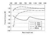
- FIG. 19 shows the relationship between the wavelength and the transmittance of various metal films, which is obtained by the transmission spectroscopic measurement of the metal film.
- the required light shielding performance in the near infrared region (design wavelength 1.5 ⁇ m) is set to ⁇ 120 dB.
- the required film thickness when various metal films are used as the conductive film 35B using the above mathematical formula (1) for example, the light-shielding performance of the W film at a wavelength of 1500 nm is ⁇ 31 dB at a thickness of 60 nm, and ⁇ 120 dB.
- the W film needs to have a thickness of 240 nm.
- the light-shielding performance of the Al film at a wavelength of 1500 nm is ⁇ 81 dB for an Al film having a thickness of 60 nm, and the thickness of the Al film is 90 nm for obtaining a light-shielding performance of ⁇ 120 dB.
- the Al film can obtain the same light-shielding performance with a thinner thickness.
- the conductive film 35B is formed by using Al, so that the conductive film 15B is formed by using W as in the first embodiment. It is possible to reduce the thickness of the conductive film 35B as compared with the case. That is, the generation of stress during the formation of the conductive film 35B is reduced. Therefore, the manufacturing yield can be improved. In addition, it is possible to prevent the implied characteristic from deteriorating.
- a barrier metal is formed between the second electrode 15 and the conductive film 35B in the opening 16H in contact with the second electrode 15 in order to prevent oxidation of Al forming the conductive film 35B. I did it. As a result, oxidation of Al that constitutes the second electrode 15, for example, by an ITO film is prevented, and stable electrical connection with low resistance between the second electrode 15 and the conductive film 35B becomes possible.
- the W film is laminated as the antireflection structure on the Al film forming the conductive film 35B.
- FIG. 20 shows the absolute reflectances of the Al single layer film, the W single layer film, and the Al/W laminated film. As compared with the Al single layer film, it can be seen that the reflectance is about the same as that of the W single layer film by forming the Al/W laminated film in which the W film having a thickness of 30 nm is laminated on the Al film. .. Therefore, it is possible to suppress the generation of ghost due to the stray light reflected by the conductive film 35B.
- Table 1 summarizes the sputtering film forming conditions and film stress of various metal films.
- Table 2 summarizes each parameter when various conductive films are used as the conductive film 35B.
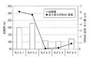
- FIG. 21 shows the relationship between the film thickness of various conductive films and the amount of warpage of the Si substrate based on Table 2.
- Samples 1 and 2 use W as a comparative example, and samples 3 to 5 correspond to the conductive film 35B of the present embodiment.
- the film thicknesses of W and Al are adjusted so that the total light shielding performance exceeds -120 dB.
- the stress indicates the value obtained when each conductive film was formed by sputtering using the conditions in Table 1, and is the amount of warpage of a Si substrate of ⁇ 200 mm wafer size generated by combining the stress values of each conductive film. Shows. A negative value for both the stress and the warp amount indicates a compression direction, and a positive value indicates an extension direction. It can be confirmed that the stress is significantly reduced in Samples 3 to 5 using Al, as compared with the conductive films using W in Samples 1 and 2.
- FIG. 22 schematically illustrates a cross-sectional configuration of a light receiving element (light receiving element 3) according to the third embodiment of the present disclosure.
- the light receiving element 3 is applied to, for example, an infrared sensor using a compound semiconductor material such as a III-V group semiconductor as in the first embodiment, and is, for example, in the visible region (for example, 380 nm to 780 nm). Less than) to a short infrared region (for example, 780 nm or more and less than 2400 nm) has a photoelectric conversion function.
- the light-receiving element 3 has a light-shielding film 37 made of, for example, black resist provided on the conductive film 15B.
- the light shielding film 37 forms the OPB region R1B together with the conductive film 15B.
- the light shielding film 37 is formed using, for example, a black resist.
- the end surface (surface 37S) of the light shielding film 37 on the element region R1 side extends, for example, on the element region R1 side of the end surface (surface 15S) of the conductive film 15B on the element region R1 side. In other words, the end surface (surface 15S) of the conductive film 15B on the element region R1 side is covered with the light shielding film 37.
- the end surface structures of the conductive film 15B and the light shielding film 37 on the element region side are not limited to this. For example, as shown in FIG.
- the end surface (surface 15S) on the region R1 side may form the same surface.
- the end surface (surface 15S) of the conductive film 15B on the element region R1 side may be projected to the element region R1 side more than the end surface (surface 37S) of the light shielding film 37 on the element region R1 side.
- the light-shielding film 37 does not necessarily have to be formed directly on the conductive film 15B, and for example, as shown in FIG. 25, the passivation film 36B is formed between the conductive film 15B and the light-shielding film 37. May be.
- the light-shielding film 37 made of, for example, black resist is provided above the conductive film 15B, so that the conductive film 15B can be thinned. That is, the generation of stress during the formation of the conductive film 35B is reduced. Therefore, the manufacturing yield can be improved. In addition, it is possible to prevent the implied characteristic from deteriorating. Further, it becomes possible to reduce the occurrence of flare.
- the passivation film 36 is formed of, for example, silicon nitride (SiN), aluminum oxide (Al 2 O 3 ), silicon oxide (SiO 2 ) and tantalum oxide (Ta). Although an example in which it is formed by using 2 O 3 ) or the like is shown, the invention is not limited to this.
- the light-receiving element 2 and the light-receiving element 3 are made of oxides, nitrides, or oxynitrides of Si, Ti, Hf, Zr, and Y, respectively, like the passivation film 16A in the first embodiment. It may be formed.
- the light receiving element 3 may have a configuration in which the passivation film 16 forming the light receiving element 1 and the conductive film 35B forming the light receiving element 2 are combined.
- FIG. 26 shows a cross-sectional configuration of a main part of the light receiving element (light receiving element 4) according to the first modification of the first to third embodiments.
- the buried layer 18 includes a first buried layer 18A and a second buried layer 18B that are stacked. Except for this point, the light receiving element 4 has the same configuration and effect as the light receiving element 1.
- FIG. 26 as an example, a sectional configuration based on the light receiving element 1 shown in FIG. 1 is shown. Further, in FIG. 26, the passivation films 16A and 16B are collectively shown as the passivation film 16 for simplification.
- the first embedded layer 18A is arranged in the peripheral region R2 and is provided closer to the light incident surface S1 than the second embedded layer 18B is. Specifically, the first burying layer 18A is arranged between the second burying layer 18B and the passivation film 16 and covers the end surface of the semiconductor layer 10S.
- the second embedded layer 18B is provided over the element region R1 and the peripheral region R2.
- the second buried layer 18B in the element region R1 is disposed between the wiring layer 10W and the semiconductor layer 10S, and together with the lower surface and the side surface of the first electrode 11, the lower surface of the semiconductor layer 10S (a surface facing the read circuit board 20). ) Is covered.
- the second buried layer 18B in the peripheral region R2 is arranged between the wiring layer 10W and the first buried layer 18A.
- the constituent material of the first buried layer 18A and the constituent material of the second buried layer 18B may be the same or different.
- the thickness of the first buried layer 18A and the thickness of the second buried layer 18B may be the same or different.
- the insulating film 17 is provided on substantially the same plane over the element region R1 and the peripheral region R2.
- the insulating film 17 is arranged between the semiconductor layer 10S in the element region R1 and the second buried layer 18B, and is arranged between the first buried layer 18A and the second buried layer 18B in the peripheral region R2. ing.
- Such a light receiving element 4 can be manufactured, for example, as follows. 27A to 30B show manufacturing steps of the light receiving element 4 in the order of steps.
- the semiconductor layer 10S on the temporary substrate 33 is formed into a plurality of chip shapes (FIG. 14B).
- the first embedded layer 18A is formed on the entire surface of the temporary substrate 33.
- the first embedding layer 18A is formed by, for example, depositing an insulating material on the entire surface of the temporary substrate 33 and then planarizing the insulating material by CMP. As a result, the first embedded layer 18A that covers the periphery of the semiconductor layer 10S is formed. At this time, the upper surface of the semiconductor layer 10S may be exposed from the first embedded layer 18A.
- the diffusion region 12A is formed in the semiconductor layer 10S using, for example, a mask formed of the insulating film 17.
- the insulating film 17 is formed on the first embedded layer 18A.
- the mask for forming the diffusion region 12A may be formed by the first burying layer 18A as shown in FIG. 28, or, as shown in FIG. 29, the first burying layer 18A.
- the insulating film 17 may be used.
- the first electrode 11 is formed in the opening of the insulating film 17 as shown in FIG. 30A.
- the second embedded layer 18B is formed on the first embedded layer 18A so as to cover the first electrode 11.
- the second burying layer 18B is formed by depositing an insulating material on the entire surface of the temporary substrate 33 and then planarizing the insulating material by CMP. Subsequent steps are the same as those described in the first embodiment (FIGS. 28D to 28J), and the light receiving element 4 is completed.
- the embedded layer 18 may be configured to have a laminated structure of the first embedded layer 18A and the second embedded layer 18B. Also in this case, the same effect as that of the first embodiment can be obtained.
- FIG. 31 shows a cross-sectional structure of a main part of the light receiving element (light receiving element 5) according to the second modification of the first to third embodiments.
- the light receiving element 5 has a color filter layer 41 and an on-chip lens (condensing lens) 42 on the light incident surface S1 of the element substrate 10 (the surface opposite to the surface facing the readout circuit board 20). Except for this point, the light receiving element 5 has the same configuration and effect as the light receiving element 1.
- FIG. 31 shows a sectional configuration based on the light receiving element 1 shown in FIG. 1 as an example. Further, in FIG. 31, the passivation films 16A and 16B are collectively shown as the passivation film 16 for simplification.
- the color filter layer 41 and the on-chip lens 42 are provided in this order on the passivation film 16 of the element substrate 10 with the flattening film 16C interposed therebetween.
- the color filter layer 41 may include an IR (Infrared) filter.
- the on-chip lens 42 collects the light incident on the light receiving element 1 in the photoelectric conversion layer 13.
- the on-chip lens 42 is made of, for example, an organic material or silicon oxide (SiO 2 ).
- SiO 2 silicon oxide
- the step between the element region R1 of the element substrate 10 and the peripheral region R2 is reduced or eliminated, and the flat light incident surface S1 is provided. Is formed.
- the on-chip lens 42 can be formed with high accuracy by using, for example, a photolithography process.
- the color filter layer 41 and the on-chip lens 42 are terminated within the element region R1.
- the flattening film 16C arranged between the passivation film 16 and the color filter layer 41 is provided, for example, from the element region R1 to the peripheral region R2, and is terminated in the peripheral region R2.
- the color filter layer 41, the on-chip lens 42, and the flattening film 16C may each be terminated at any position in the element region R1 or the peripheral region R2.
- the color filter layer 41 and the on-chip lens 42 may be provided on the light incident surface S1 of the element substrate 10. Also in this case, the same effect as that of the first embodiment can be obtained. In addition, the on-chip lens 42 can be easily formed with high accuracy on the light incident surface S1 that is flattened by the embedded layer 18.
- FIG. 33 shows the manufacturing process of the light receiving element (light receiving element 6 in FIG. 33) according to the third modification of the first to third embodiments in the order of steps.
- the light receiving element 6 is manufactured by forming a cap layer (cap layer 35 in FIG. 32A) for protecting the semiconductor layer 10S, and then bonding the semiconductor layer 10S to the temporary substrate 33 with the cap layer in between. .. Except for this point, the light-receiving element 6 has the same configuration as the light-receiving element 1, and the operation and effect thereof are also the same.
- FIG. 33 shows a cross-sectional structure based on the light receiving element 1 shown in FIG. 1 as an example. Further, in FIG. 33, the passivation films 16A and 16B are collectively shown as the passivation film 16 for simplification.
- the light receiving element 6 can be manufactured using the cap layer 35, for example, as follows.
- a semiconductor layer 10S and a cap layer 35 made of i-type InGaAs are epitaxially grown in this order on the growth substrate 31.
- the semiconductor layer 10S for example, a first contact layer 12 made of n-type InP, a photoelectric conversion layer 13 made of i-type or n-type InGaAs, and a second contact layer 14 made of n-type InP are formed in this order. ..
- the cap layer 35 is for preventing the semiconductor layer 10S and the adhesive layer B for joining the semiconductor layer 10S to the temporary substrate 33 from being in direct contact with each other. If the process is advanced while the adhesive layer B is in contact with the semiconductor layer 10S, the characteristics of the semiconductor layer 10S may deteriorate. Alternatively, the semiconductor layer 10S may be peeled off from the temporary substrate 33. The semiconductor layer 10S may be peeled off from the adhesive layer B. By forming the cap layer 35 between the semiconductor layer 10S and the adhesive layer B, it is possible to suppress such characteristic deterioration and film peeling.
- the cap layer 35 may be any semiconductor material that can be epitaxially grown on the semiconductor layer 10S (more specifically, the second contact layer 14), and for example, InGaAs or InAsSb can be used.
- the adhesive layer B containing, for example, silicon oxide (SiO 2 ) is formed on the cap layer 35.
- the growth substrate 31 is joined to the large-diameter temporary substrate 33 with the adhesive layer B interposed therebetween.
- the cap layer 35 is interposed between the adhesive layer B and the second contact layer 14.
- TEOS tetraethoxysilane
- SiO 2 silicon oxide
- the growth substrate 31 is removed, the semiconductor layer 10S is molded, the diffusion region 12A is formed by pure substance diffusion, the first electrode 11 is formed and embedded.
- the layer 18 is formed in this order (see FIGS. 11A to 17C). Thereafter, as shown in FIG. 32C, the wiring layer 10W is formed on the embedded layer 18.
- the buried layer 18 that fills the step between the semiconductor layer 10S and the temporary substrate 33 is formed, the occurrence of defects in the manufacturing process due to these step can be suppressed. ..
- the cap layer 35 is interposed between the adhesive layer B and the second contact layer 14 in the steps of removing the growth substrate 31, forming the diffusion region 12A, forming the wiring layer 10W, etc., the semiconductor layer 10S. It is possible to suppress the deterioration of the characteristics and the occurrence of film peeling.
- the temporary substrate 33 is attached to the read circuit board 20 with the wiring layer 10W interposed therebetween in the same manner as described in the first embodiment (FIG. 32D).
- the temporary substrate 33, the adhesive layer B, and the cap layer 35 are removed in this order to expose the second contact layer 14.
- the removal of the temporary substrate 33 is performed in the same manner as described in the first embodiment.
- the adhesive layer B and the cap layer 35 can be removed by, for example, wet etching.
- wet etching of the adhesive layer B for example, HF (Hydrogen Fluoride) or BHF (Buffered Hydrogen Fluoride) can be used.
- a mixed solution of an acid and an oxidizing agent can be used for the wet etching of the cap layer 35.
- the acid for example, HF, hydrochloric acid (HCl), phosphoric acid (H 3 PO 4 ) or the like can be used, and as the oxidizing agent, for example, hydrogen peroxide water or ozone water can be used.
- the adhesive layer B and the cap layer 35 can be removed by dry etching, they are preferably removed by wet etching (described later).
- FIG. 34A is an example of an enlarged view of the portion R shown in FIG. 32E.
- the area where the adhesive layer B and the cap layer 35 are removed is smaller than the area of the semiconductor layer 10S in plan view, for example.
- the periphery of the semiconductor layer 10S on the side of the light incident surface S1 the surface opposite to the surface facing the readout circuit substrate 20
- the cap layer 35 and the adhesive layer on the end portion of the second contact layer 14. B remains.
- the cap layer 35 may be dented with respect to the adhesive layer B or may be protruded.
- the light-receiving element 6 is completed in the same manner as described in the first embodiment (see FIGS. 17H to 17J).
- FIG. 33 shows an example of a cross-sectional structure of a main part of the light-receiving element 6 manufactured in this way.
- FIG. 34B is an example in which the portion R shown in FIG. 33 is enlarged.
- the second electrode 15 and the passivation film 16 may be formed with the cap layer 35 and the adhesive layer B remaining.
- the second electrode 15 contacts the second contact layer 14 and also contacts the cap layer 35 and the adhesive layer B.
- the embedded layer 18 protrudes toward the light incident surface S1 (opposite the read circuit board 20) side of the semiconductor layer 10S by the thickness of the cap layer 35 and the adhesive layer B.
- the opening formed by removing the adhesive layer B and the cap layer 35 that is, the opening exposing the second contact layer 14 preferably has a tapered shape as shown in FIG. 34C.
- the second electrode 15 By forming the second electrode 15 in such a tapered opening, the coverage of the second electrode 15 is improved.
- the taper-shaped opening is formed by removing the adhesive layer B and the cap layer 35 using wet etching. Therefore, the adhesive layer B and the cap layer 35 are preferably removed by wet etching.
- FIG. 35A shows another example in which the portion R shown in FIG. 32E is enlarged and FIG. 35B shows the portion R shown in FIG. 33 in an enlarged manner.
- the area where the adhesive layer B and the cap layer 35 are removed may be the same as the area of the semiconductor layer 10S in plan view, for example.
- the cap layer 35 on the end of the second contact layer 14 is removed.
- the upper surface of the second contact layer 14 (the surface on the light incident surface S1 side) and the lower surface of the adhesive layer B (the surface on the read circuit board 20 side) are displaced, A step due to the cap layer 35 is formed between them.
- the second electrode 15 is in contact with the second contact layer 14 and the adhesive layer B.
- the opening formed by removing the adhesive layer B and the cap layer 35, that is, the opening exposing the second contact layer 14 preferably has a tapered shape as shown in FIG. 35C.
- FIG. 36A shows another example in which the portion R shown in FIG. 32E is enlarged and FIG. 36B shows the portion R shown in FIG. 33 in an enlarged manner.
- the area where the adhesive layer B and the cap layer 35 are removed may be larger than the area of the semiconductor layer 10S in plan view, for example.
- the cap layer 35 on the end of the second contact layer 14 is removed.
- a recess 18R due to etching is formed between the end surface of the semiconductor layer 10S and the buried layer 18.
- the second electrode 15 is in contact with the second contact layer 14, fills the recess 18R, and is in contact with the adhesive layer B.
- the opening formed by removing the adhesive layer B and the cap layer 35, that is, the opening exposing the second contact layer 14 preferably has a tapered shape as shown in FIG. 36C.
- the region where the adhesive layer B and the cap layer 35 are removed may be further enlarged so that the adhesive layer B is removed together with the cap layer 35.
- the buried layer 18 is formed in the same manner as described in the above light receiving element 1, so that the manufacturing process is defective due to the step between the semiconductor layer 10S and the temporary substrate 33. Can be suppressed. Further, since the cap layer 35 is formed, contact between the semiconductor layer 10S (second contact layer 14) and the adhesive layer B can be prevented.
- the cap layer 35 may remain on the end of the second contact layer 14 (FIGS. 34A to 34C), or the cap layer 35 may be completely removed.
- a step (FIGS. 35A to 35C) between the upper surface of the second contact layer 14 and the lower surface of the adhesive layer B, or the end surface of the semiconductor layer 10S and the buried portion.
- a recess 18R (FIGS. 36A to 36D) between the layer 18 and the layer 18 is provided.
- the embedded layer 18 protrudes toward the light incident surface S1 side of the semiconductor layer 10S by the thickness of the cap layer 35 and the adhesive layer B.
- Modification 4> 37 and 38 schematically show the cross-sectional configurations of the light receiving elements (light receiving elements 7A and 7B) according to the modified example 4 of the second and third embodiments.
- the first contact layer 52, the photoelectric conversion layer 53, and the second contact layer 54 form a semiconductor layer 50S common to the plurality of pixels P.
- the second electrode 55 having a light blocking property is provided between the adjacent pixels P on the incident surface S1 side. Except for this point, the light receiving elements 7A and 7B have the same configuration as that of the light receiving element 1, and the operation and effect thereof are also the same.
- the element substrate 50 is arranged such that the interlayer insulating films 58B and 58A, the first contact layer 52, the photoelectric conversion layer 53, the second contact layer 54, and the second contact layer 54 from the position close to the read circuit substrate 60. It has two electrodes 55 in this order. Further, a passivation film 59 is provided on the second contact layer 54, the second electrode 55, the buried layer 57, and the through electrode 57V. A wiring layer 50W including the first electrode 51 is provided on the interlayer insulating film 58. The wiring layer 50W has contact electrodes 58EA and 58EB and a dummy electrode 58ED in the interlayer insulating films 58A and 58B.
- the surface of the semiconductor layer 50S facing the wiring layer 50W and the end surface (side surface) are covered with an insulating film 56.
- the read circuit board 60 includes a wiring layer 60W that contacts the bonding surface S2 of the element substrate 50, and a semiconductor substrate 61 that faces the element substrate 50 with the wiring layer 60W in between.
- the second electrode 55 has a structure in which a cap layer 55A and a light shielding film 55B are stacked in this order, and is, for example, a grid pattern between adjacent pixels P on the second contact layer 54 (light incident surface side). It is provided in.
- the light shielding film 55B can be formed by using an aluminum (Al) film, for example, like the conductive film 35B in the second embodiment.
- a tungsten (W) film, a copper (Cu) film, a silver (Ag) film, or the like may be used.
- the light shielding film 55B is preferably laminated on the cap layer 55A via a barrier metal film such as a titanium (Ti) film or a titanium nitride (TiN) film. As a result, ohmic contact is formed between the cap layer 55A and the light shielding film 55B.
- a barrier metal film such as a titanium (Ti) film or a titanium nitride (TiN) film.
- a light-shielding film 37 made of, for example, a black resist may be laminated on the light-shielding film 55B near the peripheral region R2 of the element region R1.
- the second electrode 55 is formed, for example, by patterning the light shielding film 55B by dry etching and then patterning the cap layer 55A by wet etching using the light shielding film 55B as a metal mask.
- the cross-sectional shape of the cap layer 55A (for example, N+InGaAs layer) patterned in a lattice pattern has a feature that it varies depending on the crystal plane orientation.
- a 100-face InGaAs/InP crystal is processed into a reverse taper in the (011) plane cross-sectional direction and a forward taper in a direction rotated by 90° with respect to the (011) plane.
- the readout circuit board 60 is a so-called ROIC (Readout integrated circuit), and the wiring layer 60W in contact with the bonding surface S2 of the element substrate 50 and the wiring layer 60W are placed between the element substrate 50. And a semiconductor substrate 61 facing to.
- the semiconductor substrate 61 is for supporting the wiring layer 60W, and is made of, for example, silicon (Si).
- the wiring layer 60W has, for example, contact electrodes 62EA and 62EB, a dummy electrode 62ED, a pixel circuit 62CA, a wiring 62CB, and a pad electrode 62P in an interlayer insulating film 62 (62A and 62B).
- the interlayer insulating films 62A and 62B are made of, for example, an inorganic insulating material.
- the inorganic insulating material include silicon nitride (SiN), aluminum oxide (Al 2 O 3 ), silicon oxide (SiO 2 ) and hafnium oxide (HfO 2 ).
- the interlayer insulating films 62A and 62B may be formed by using different inorganic insulating materials or may be formed by using the same inorganic insulating material.
- the second electrode 55 has a laminated structure of a cap layer 55A and a light shielding film 55B formed by using, for example, a metal film. As described above, by forming the cap layer 55A and the light shielding film 55B in this order, it is not necessary to form a transparent electrode or thicken the second contact layer 54. Further, damage to the photoelectric conversion portion (specifically, the second contact layer 54) at the time of patterning the light shielding film 55B is reduced. Therefore, the sensitivity can be improved.
- FIG. 39 schematically shows a cross-sectional structure of the light receiving element (light receiving element 8) according to the modified example 5 of the first to third embodiments.
- the light receiving element 8 has a laminated structure of an element substrate 10 containing a compound semiconductor material and a semiconductor layer containing silicon (Si) (semiconductor layer 71S, second semiconductor layer). Except for this point, the light receiving element 8 has the same configuration as the light receiving element 1, and the operation and effect are also the same.
- FIG. 39 shows a cross-sectional structure based on the light receiving element 1 shown in FIG. 1 as an example. Further, in FIG. 39, the passivation films 16A and 16B are collectively shown as the passivation film 16 for simplification.
- the light receiving element 8 has a wiring layer 71W electrically connected to the semiconductor layer 71S, a semiconductor layer 71S, a color filter layer 41, and an on-chip lens in this order on the light incident surface S1 of the element substrate 10.
- the semiconductor layer 71S is provided with a photodiode PD having a pn junction for each pixel P.
- the wiring layer 71W includes a plurality of wirings, and for example, the signal charges generated by the photodiode PD move to the readout circuit substrate 20 for each pixel P by the wiring layer 71W.
- photoelectric conversion of light having wavelengths in the visible region and the infrared region is performed.
- light having a wavelength in the visible region enters the semiconductor layer 71S via the on-chip lens 42 and the color filter layer 41, and is photoelectrically converted by the photodiode PD.
- light having a wavelength in the infrared region passes through the semiconductor layer 71S and is photoelectrically converted by the photoelectric conversion layer 13 of the element substrate 10.
- the signal charge generated in the photodiode PD and the signal charge generated in the photoelectric conversion layer 13 are read by the read circuit board 20.
- the buried layer 18 is formed in the same manner as described in the light-receiving elements 1 and 2, so that the manufacturing process is defective due to the step between the semiconductor layer 10S and the temporary substrate 33. Can be suppressed. Further, since the semiconductor layer 71S is laminated on the element substrate 10, one pixel P can photoelectrically convert light having a wavelength in the visible region and an infrared region. Therefore, it is possible to increase the amount of information that can be acquired from one pixel P.
- the light-receiving element 1 (or the light-receiving elements 1, 2, 3, 4, 5, 6, 7A, 7B, 8 and hereafter, collectively referred to as the light-receiving element 1) described in the above-described embodiments is, for example, Applied.
- This image sensor is, for example, an infrared image sensor.
- FIG. 40 shows a schematic configuration of the electronic device 9 (camera) as an example.
- the electronic device 9 is, for example, a camera capable of shooting a still image or a moving image, and includes an image sensor 9A including the light receiving element 1, an optical system (optical lens) 310, a shutter device 311, an image sensor 9A and a shutter. It has a drive unit 313 that drives the device 311 and a signal processing unit 312.
- the optical system 310 guides image light (incident light) from a subject to the image sensor 9A.
- the optical system 310 may be composed of a plurality of optical lenses.
- the shutter device 311 controls a light irradiation period and a light shielding period for the image sensor 9A.
- the drive unit 313 controls the transfer operation of the image sensor 9A and the shutter operation of the shutter device 311.
- the signal processing unit 312 performs various kinds of signal processing on the signal output from the image sensor 9A.
- the video signal Dout after the signal processing is stored in a storage medium such as a memory or output to a monitor or the like.
- the light receiving element 1 described in the present embodiment and the like can be applied to the following electronic devices (capsule endoscope and moving body such as a vehicle).
- Application example 1 (endoscopic surgery system)>
- the technology according to the present disclosure can be applied to various products.
- the technology according to the present disclosure may be applied to an endoscopic surgery system.
- FIG. 41 is a diagram showing an example of a schematic configuration of an endoscopic surgery system to which the technology according to the present disclosure (the present technology) can be applied.
- FIG. 41 illustrates a situation in which an operator (doctor) 11131 is operating on a patient 11132 on a patient bed 11133 using the endoscopic surgery system 11000.
- the endoscopic surgery system 11000 includes an endoscope 11100, other surgical tools 11110 such as a pneumoperitoneum tube 11111 and an energy treatment tool 11112, and a support arm device 11120 that supports the endoscope 11100.
- a cart 11200 on which various devices for endoscopic surgery are mounted.
- the endoscope 11100 includes a lens barrel 11101 into which a region having a predetermined length from the distal end is inserted into the body cavity of the patient 11132, and a camera head 11102 connected to the base end of the lens barrel 11101.
- the endoscope 11100 configured as a so-called rigid endoscope having the rigid barrel 11101 is illustrated, but the endoscope 11100 may be configured as a so-called flexible mirror having a flexible barrel. Good.
- An opening in which an objective lens is fitted is provided at the tip of the lens barrel 11101.
- a light source device 11203 is connected to the endoscope 11100, and the light generated by the light source device 11203 is guided to the tip of the lens barrel by a light guide extending inside the lens barrel 11101. It is irradiated toward the observation target in the body cavity of the patient 11132 via the lens.
- the endoscope 11100 may be a direct-viewing endoscope, or may be a perspective or side-viewing endoscope.
- An optical system and an image pickup device are provided inside the camera head 11102, and reflected light (observation light) from an observation target is condensed on the image pickup device by the optical system.
- the observation light is photoelectrically converted by the imaging element, and an electric signal corresponding to the observation light, that is, an image signal corresponding to the observation image is generated.
- the image signal is transmitted as RAW data to a camera control unit (CCU: Camera Control Unit) 11201.
- CCU Camera Control Unit
- the CCU 11201 is composed of a CPU (Central Processing Unit), a GPU (Graphics Processing Unit), and the like, and controls the operations of the endoscope 11100 and the display device 11202 in a centralized manner. Further, the CCU 11201 receives the image signal from the camera head 11102, and performs various image processing such as development processing (demosaic processing) on the image signal for displaying an image based on the image signal.
- image processing such as development processing (demosaic processing)
- the display device 11202 displays an image based on an image signal subjected to image processing by the CCU 11201 under the control of the CCU 11201.
- the light source device 11203 is composed of a light source such as an LED (light emitting diode), and supplies irradiation light to the endoscope 11100 when photographing a surgical site or the like.
- a light source such as an LED (light emitting diode)
- the input device 11204 is an input interface for the endoscopic surgery system 11000.
- the user can input various kinds of information and instructions to the endoscopic surgery system 11000 via the input device 11204.
- the user inputs an instruction to change the imaging conditions (type of irradiation light, magnification, focal length, etc.) by the endoscope 11100.
- the treatment instrument control device 11205 controls driving of the energy treatment instrument 11112 for cauterization of tissue, incision, sealing of blood vessel, or the like.
- the pneumoperitoneum device 11206 is used to inflate the body cavity of the patient 11132 through the pneumoperitoneum tube 11111 in order to inflate the body cavity of the patient 11132 for the purpose of securing the visual field by the endoscope 11100 and the working space of the operator.
- the recorder 11207 is a device capable of recording various information regarding surgery.
- the printer 11208 is a device capable of printing various types of information regarding surgery in various formats such as text, images, and graphs.
- the light source device 11203 that supplies irradiation light to the endoscope 11100 when imaging a surgical site can be configured by, for example, an LED, a laser light source, or a white light source configured by a combination thereof.
- a white light source is formed by a combination of RGB laser light sources
- the output intensity and output timing of each color (each wavelength) can be controlled with high accuracy, so that the light source device 11203 adjusts the white balance of the captured image. It can be carried out.
- the laser light from each of the RGB laser light sources is irradiated on the observation target in a time division manner, and the drive of the image pickup device of the camera head 11102 is controlled in synchronization with the irradiation timing so as to correspond to each of the RGB. It is also possible to take the captured image in a time division manner. According to this method, a color image can be obtained without providing a color filter on the image sensor.
- the drive of the light source device 11203 may be controlled so as to change the intensity of the output light at predetermined time intervals.
- the drive of the image sensor of the camera head 11102 in synchronization with the timing of changing the intensity of the light to acquire an image in a time-division manner and combining the images, a high dynamic image without so-called blackout and blown-out highlights is obtained. An image of the range can be generated.
- the light source device 11203 may be configured to be able to supply light in a predetermined wavelength band corresponding to special light observation.
- special light observation for example, by utilizing the wavelength dependence of the absorption of light in body tissues, by irradiating a narrow band of light as compared with the irradiation light (that is, white light) during normal observation, the mucosal surface layer
- the so-called narrow band imaging is performed in which a predetermined tissue such as blood vessels is imaged with high contrast.
- fluorescence observation in which an image is obtained by fluorescence generated by irradiating the excitation light may be performed.
- the light source device 11203 can be configured to be capable of supplying narrowband light and/or excitation light compatible with such special light observation.
- FIG. 42 is a block diagram showing an example of the functional configuration of the camera head 11102 and CCU 11201 shown in FIG.
- the camera head 11102 includes a lens unit 11401, an imaging unit 11402, a driving unit 11403, a communication unit 11404, and a camera head control unit 11405.
- the CCU 11201 has a communication unit 11411, an image processing unit 11412, and a control unit 11413.
- the camera head 11102 and the CCU 11201 are communicably connected to each other by a transmission cable 11400.
- the lens unit 11401 is an optical system provided at the connecting portion with the lens barrel 11101.
- the observation light taken in from the tip of the lens barrel 11101 is guided to the camera head 11102 and enters the lens unit 11401.
- the lens unit 11401 is configured by combining a plurality of lenses including a zoom lens and a focus lens.
- the number of image pickup elements forming the image pickup unit 11402 may be one (so-called single-plate type) or plural (so-called multi-plate type).
- image signals corresponding to R, G, and B may be generated by the respective image pickup elements, and these may be combined to obtain a color image.
- the image capturing unit 11402 may be configured to include a pair of image capturing elements for respectively acquiring image signals for the right eye and the left eye corresponding to 3D (dimensional) display.
- the 3D display enables the operator 11131 to more accurately understand the depth of the living tissue in the operation site.
- a plurality of lens units 11401 may be provided corresponding to each image pickup element.
- the image pickup unit 11402 does not necessarily have to be provided on the camera head 11102.
- the imaging unit 11402 may be provided inside the lens barrel 11101 immediately after the objective lens.
- the drive unit 11403 is composed of an actuator, and moves the zoom lens and the focus lens of the lens unit 11401 by a predetermined distance along the optical axis under the control of the camera head control unit 11405. Accordingly, the magnification and focus of the image captured by the image capturing unit 11402 can be adjusted appropriately.
- the communication unit 11404 is composed of a communication device for transmitting and receiving various information to and from the CCU11201.
- the communication unit 11404 transmits the image signal obtained from the imaging unit 11402 as RAW data to the CCU 11201 via the transmission cable 11400.
- the communication unit 11404 receives a control signal for controlling the driving of the camera head 11102 from the CCU 11201 and supplies it to the camera head control unit 11405.
- the control signal includes, for example, information that specifies the frame rate of the captured image, information that specifies the exposure value at the time of capturing, and/or information that specifies the magnification and focus of the captured image. Contains information about the condition.
- the image capturing conditions such as the frame rate, the exposure value, the magnification, and the focus may be appropriately designated by the user, or may be automatically set by the control unit 11413 of the CCU 11201 based on the acquired image signal. Good. In the latter case, the so-called AE (Auto Exposure) function, AF (Auto Focus) function, and AWB (Auto White Balance) function are installed in the endoscope 11100.
- AE Auto Exposure
- AF Auto Focus
- AWB Auto White Balance
- the camera head control unit 11405 controls driving of the camera head 11102 based on a control signal from the CCU 11201 received via the communication unit 11404.
- the communication unit 11411 is composed of a communication device for transmitting and receiving various information to and from the camera head 11102.
- the communication unit 11411 receives the image signal transmitted from the camera head 11102 via the transmission cable 11400.
- the communication unit 11411 transmits a control signal for controlling the driving of the camera head 11102 to the camera head 11102.
- the image signal and the control signal can be transmitted by electric communication, optical communication, or the like.
- the image processing unit 11412 performs various kinds of image processing on the image signal that is the RAW data transmitted from the camera head 11102.
- the control unit 11413 performs various controls regarding imaging of a surgical site or the like by the endoscope 11100 and display of a captured image obtained by imaging the surgical site or the like. For example, the control unit 11413 generates a control signal for controlling the driving of the camera head 11102.
- control unit 11413 causes the display device 11202 to display a captured image of the surgical site or the like based on the image signal subjected to the image processing by the image processing unit 11412.
- the control unit 11413 may recognize various objects in the captured image using various image recognition techniques.
- the control unit 11413 detects a surgical instrument such as forceps, a specific living body part, bleeding, and a mist when the energy treatment instrument 11112 is used by detecting the shape and color of the edge of the object included in the captured image. Can be recognized.
- the control unit 11413 may use the recognition result to superimpose and display various types of surgery support information on the image of the operation unit. By displaying the surgery support information in a superimposed manner and presenting it to the operator 11131, the burden on the operator 11131 can be reduced and the operator 11131 can surely proceed with the surgery.
- the transmission cable 11400 that connects the camera head 11102 and the CCU 11201 is an electric signal cable that supports electric signal communication, an optical fiber that supports optical communication, or a composite cable of these.
- wired communication is performed using the transmission cable 11400, but communication between the camera head 11102 and the CCU 11201 may be performed wirelessly.
- the technology according to the present disclosure can be applied to the imaging unit 11402 among the configurations described above.
- a clearer image of the surgical site can be obtained, so that the operator can surely confirm the surgical site.
- the endoscopic surgery system has been described as an example, but the technology according to the present disclosure may be applied to, for example, a microscopic surgery system or the like.
- the technology according to the present disclosure can be applied to various products.
- the technology according to the present disclosure is realized as a device mounted on any type of moving body such as an automobile, an electric vehicle, a hybrid electric vehicle, a motorcycle, a bicycle, a personal mobility, an airplane, a drone, a ship, and a robot. May be.
- FIG. 43 is a block diagram showing a schematic configuration example of a vehicle control system which is an example of a mobile body control system to which the technology according to the present disclosure can be applied.
- the vehicle control system 12000 includes a plurality of electronic control units connected via a communication network 12001.
- the vehicle control system 12000 includes a drive system control unit 12010, a body system control unit 12020, a vehicle exterior information detection unit 12030, a vehicle interior information detection unit 12040, and an integrated control unit 12050.
- a microcomputer 12051, a voice image output unit 12052, and an in-vehicle network I/F (Interface) 12053 are shown as a functional configuration of the integrated control unit 12050.
- the drive system control unit 12010 controls the operation of devices related to the drive system of the vehicle according to various programs.
- the drive system control unit 12010 includes a drive force generation device for generating a drive force of a vehicle such as an internal combustion engine or a drive motor, a drive force transmission mechanism for transmitting the drive force to wheels, and a steering angle of the vehicle. It functions as a steering mechanism for adjusting and a control device such as a braking device for generating a braking force of the vehicle.
- the body system control unit 12020 controls operations of various devices mounted on the vehicle body according to various programs.
- the body system control unit 12020 functions as a keyless entry system, a smart key system, a power window device, or a control device for various lamps such as a head lamp, a back lamp, a brake lamp, a winker, or a fog lamp.
- radio waves or signals of various switches transmitted from a portable device that substitutes for a key can be input to the body system control unit 12020.
- the body system control unit 12020 accepts the input of these radio waves or signals and controls the vehicle door lock device, the power window device, the lamp, and the like.
- the vehicle exterior information detection unit 12030 detects information outside the vehicle equipped with the vehicle control system 12000.
- the imaging unit 12031 is connected to the vehicle exterior information detection unit 12030.
- the vehicle exterior information detection unit 12030 causes the image capturing unit 12031 to capture an image outside the vehicle and receives the captured image.
- the vehicle exterior information detection unit 12030 may perform object detection processing or distance detection processing such as people, vehicles, obstacles, signs, or characters on the road surface based on the received image.
- the image pickup unit 12031 is an optical sensor that receives light and outputs an electric signal according to the amount of received light.
- the imaging unit 12031 can output the electric signal as an image or as distance measurement information.
- the light received by the imaging unit 12031 may be visible light or invisible light such as infrared light.
- the in-vehicle information detection unit 12040 detects in-vehicle information.
- the in-vehicle information detection unit 12040 is connected with, for example, a driver state detection unit 12041 that detects the state of the driver.
- the driver state detection unit 12041 includes, for example, a camera that captures an image of the driver, and the in-vehicle information detection unit 12040 determines the degree of fatigue or concentration of the driver based on the detection information input from the driver state detection unit 12041. It may be calculated or it may be determined whether or not the driver is asleep.
- the microcomputer 12051 calculates the control target value of the driving force generation device, the steering mechanism or the braking device based on the information on the inside and outside of the vehicle acquired by the outside information detection unit 12030 or the inside information detection unit 12040, and the drive system control unit.
- a control command can be output to 12010.
- the microcomputer 12051 realizes functions of ADAS (Advanced Driver Assistance System) including avoidance or impact mitigation of a vehicle, follow-up traveling based on an inter-vehicle distance, vehicle speed maintenance traveling, a vehicle collision warning, or a vehicle lane departure warning. It is possible to perform cooperative control for the purpose.
- ADAS Advanced Driver Assistance System
- the microcomputer 12051 controls the driving force generation device, the steering mechanism, the braking device, or the like based on the information around the vehicle acquired by the vehicle exterior information detection unit 12030 or the vehicle interior information detection unit 12040, thereby It is possible to perform cooperative control for the purpose of autonomous driving or the like that autonomously travels without depending on the operation.
- the microcomputer 12051 can output a control command to the body system control unit 12020 based on the information on the outside of the vehicle acquired by the outside information detection unit 12030.
- the microcomputer 12051 controls the headlamp according to the position of the preceding vehicle or the oncoming vehicle detected by the vehicle exterior information detection unit 12030, and performs cooperative control for the purpose of antiglare such as switching the high beam to the low beam. It can be carried out.
- the voice image output unit 12052 transmits an output signal of at least one of a voice and an image to an output device capable of visually or audibly notifying information to an occupant of the vehicle or the outside of the vehicle.
- an audio speaker 12061, a display unit 12062, and an instrument panel 12063 are illustrated as output devices.
- the display unit 12062 may include at least one of an onboard display and a head-up display, for example.
- FIG. 44 is a diagram showing an example of the installation position of the imaging unit 12031.
- the image capturing unit 12031 includes image capturing units 12101, 12102, 12103, 12104, and 12105.
- the image capturing units 12101, 12102, 12103, 12104, and 12105 are provided, for example, at positions such as the front nose of the vehicle 12100, the side mirrors, the rear bumper, the back door, and the upper portion of the windshield inside the vehicle.
- the image capturing unit 12101 provided on the front nose and the image capturing unit 12105 provided on the upper part of the windshield in the vehicle interior mainly acquire an image in front of the vehicle 12100.
- the imaging units 12102 and 12103 provided in the side mirrors mainly acquire images of the side of the vehicle 12100.
- the image capturing unit 12104 provided in the rear bumper or the back door mainly acquires an image behind the vehicle 12100.
- the imaging unit 12105 provided on the upper part of the windshield inside the vehicle is mainly used for detecting a preceding vehicle, a pedestrian, an obstacle, a traffic signal, a traffic sign, a lane, or the like.
- FIG. 44 shows an example of the shooting range of the imaging units 12101 to 12104.
- the imaging range 12111 indicates the imaging range of the imaging unit 12101 provided on the front nose
- the imaging ranges 12112 and 12113 indicate the imaging ranges of the imaging units 12102 and 12103 provided on the side mirrors
- the imaging range 12114 indicates The imaging range of the imaging part 12104 provided in a rear bumper or a back door is shown. For example, by overlaying the image data captured by the image capturing units 12101 to 12104, a bird's-eye view image of the vehicle 12100 viewed from above can be obtained.
- At least one of the imaging units 12101 to 12104 may have a function of acquiring distance information.
- at least one of the image capturing units 12101 to 12104 may be a stereo camera including a plurality of image capturing elements, or may be an image capturing element having pixels for phase difference detection.
- the microcomputer 12051 based on the distance information obtained from the imaging units 12101 to 12104, the distance to each three-dimensional object in the imaging range 12111 to 12114 and the temporal change of this distance (relative speed with respect to the vehicle 12100). By determining, the closest three-dimensional object on the traveling path of the vehicle 12100, which is traveling in the substantially same direction as the vehicle 12100 at a predetermined speed (for example, 0 km/h or more), can be extracted as a preceding vehicle. it can. Further, the microcomputer 12051 can set an inter-vehicle distance to be secured in front of the preceding vehicle in advance, and can perform automatic brake control (including follow-up stop control), automatic acceleration control (including follow-up start control), and the like. In this way, it is possible to perform cooperative control for the purpose of autonomous driving or the like that autonomously travels without depending on the operation of the driver.
- automatic brake control including follow-up stop control
- automatic acceleration control including follow-up start control
- the microcomputer 12051 uses the distance information obtained from the imaging units 12101 to 12104 to convert three-dimensional object data regarding a three-dimensional object to other three-dimensional objects such as two-wheeled vehicles, ordinary vehicles, large vehicles, pedestrians, and utility poles. It can be classified, extracted, and used for automatic avoidance of obstacles. For example, the microcomputer 12051 distinguishes obstacles around the vehicle 12100 into obstacles visible to the driver of the vehicle 12100 and obstacles difficult to see. Then, the microcomputer 12051 determines the collision risk indicating the risk of collision with each obstacle, and when the collision risk is equal to or higher than the set value and there is a possibility of collision, the microcomputer 12051 outputs the audio through the audio speaker 12061 and the display unit 12062. A driver can be assisted for avoiding a collision by outputting an alarm to the driver and performing forced deceleration or avoidance steering through the drive system control unit 12010.
- At least one of the imaging units 12101 to 12104 may be an infrared camera that detects infrared rays.
- the microcomputer 12051 can recognize a pedestrian by determining whether or not a pedestrian is present in the images captured by the imaging units 12101 to 12104. To recognize such a pedestrian, for example, a procedure of extracting a feature point in an image captured by the image capturing units 12101 to 12104 as an infrared camera, and a pattern matching process on a series of feature points indicating an outline of an object are performed to determine whether the pedestrian is a pedestrian. It is performed by the procedure of determining.
- the audio image output unit 12052 causes the recognized pedestrian to have a rectangular contour line for emphasis.
- the display unit 12062 is controlled so as to superimpose and display. Further, the audio image output unit 12052 may control the display unit 12062 to display an icon indicating a pedestrian or the like at a desired position.
- the technology according to the present disclosure can be applied to the imaging unit 12031 among the configurations described above.
- the technology according to the present disclosure can be applied to the image capturing unit 12031, a captured image that is easier to see can be obtained, and thus fatigue of the driver can be reduced.
- the light receiving element 1 described in the present embodiment and the like can be applied to electronic devices such as a surveillance camera, a biometric authentication system, and thermography.
- the surveillance camera is, for example, a night vision system (night vision).
- night vision night vision
- thermography enables non-contact temperature measurement. Thermography can also detect temperature distribution and heat generation.
- the light receiving element 1 can be applied to an electronic device that detects flame, moisture, gas, or the like.
- the modified examples 1 to 5 and the application examples and the application examples have been described above, the present disclosure is not limited to the above embodiments and the like, and various modifications may be made. It is possible.
- the modified examples 1 to 3 and 5 have been described as modified examples of the first embodiment, but can also be applied as modified examples of the second embodiment and the third embodiment.
- the layer structure of the light receiving element described in the above embodiments and the like is an example, and may further include other layers.
- the material and thickness of each layer are also examples, and are not limited to the above.
- the semiconductor layer 10S is configured by the first contact layer 12, the photoelectric conversion layer 13, and the second contact layer 14 has been described, but the semiconductor layer 10S includes the photoelectric conversion layer 13. Good.
- the first contact layer 12 and the second contact layer 14 may not be provided, or other layers may be included.
- the signal charge is a hole
- the signal charge may be an electron
- the diffusion region may include n-type impurities.
- the semiconductor element of the present technology may be other than the light receiving element.
- the semiconductor element of the present technology may be a light emitting element.
- the present disclosure may have the following configurations.
- the first present technology having the following configuration, since the insulating layer having non-reducing property is provided on the second electrode having a light transmitting property, the adhesion between the second electrode and the insulating layer is improved.
- the conductive film provided on the insulating layer and electrically connected to the second electrode through the opening provided near the peripheral region of the element region is made of aluminum (Al). Since it is formed by the above method, the thickness of the conductive film is reduced.
- a black resist is further formed on the conductive film which is provided on the insulating layer and electrically connected to the second electrode through the opening provided near the peripheral region of the element region.
- An element substrate having an element region provided by laminating a wiring layer and a first semiconductor layer containing a compound semiconductor material, and a peripheral region outside the element region; A read circuit board that faces the first semiconductor layer with the wiring layer in between and is electrically connected to the first semiconductor layer through the wiring layer; A first electrode provided on the wiring layer and electrically connected to the first semiconductor layer; A second electrode facing the first electrode with the first semiconductor layer in between; A semiconductor element provided on the second electrode and having an insulating layer having a non-reducing property.
- the insulating layer contains any one of oxide (M x O y ), nitride (M x N y ) and oxynitride (M x O y N z ).
- M is any one of silicon (Si), titanium (Ti), hafnium (Hf), zirconium (Zr) and yttrium (Y).
- x, y and z are integers of 1 or more.
- the insulating layer is formed of an oxide film having a film density of 2.0 g/cm 3 or more and 8.0 g/cm 3 or less.
- the insulating layer has an opening near the peripheral region of the element region, In any one of (1) to (4) above, further comprising a conductive film electrically connected to the second electrode through the opening in the vicinity of the peripheral region and above the insulating layer.
- (6) The semiconductor element according to (5), wherein the conductive film is formed using aluminum (Al).
- the element substrate further has a through hole penetrating to the read circuit substrate in the peripheral region,
- the said element substrate is a semiconductor element as described in said (13) or (14) which further has a buried layer which surrounds the said 1st semiconductor layer in the said peripheral region.
- the compound semiconductor material absorbs light having a wavelength in the infrared region.
- An element substrate having an element region provided by laminating a wiring layer and a first semiconductor layer containing a compound semiconductor material, and a peripheral region outside the element region;
- a read circuit board that faces the first semiconductor layer with the wiring layer in between and is electrically connected to the first semiconductor layer through the wiring layer;
- a first electrode provided on the wiring layer and electrically connected to the first semiconductor layer;
- a second electrode facing the first electrode with the first semiconductor layer in between;
- An insulating layer provided on the second electrode and having an opening near the peripheral region of the element region;
- a semiconductor element comprising: a conductive film provided above the insulating layer and including aluminum (Al) electrically connected to the second electrode through the opening.
- An element substrate having an element region provided by laminating a wiring layer and a first semiconductor layer containing a compound semiconductor material, and a peripheral region outside the element region;
- a read circuit board that faces the first semiconductor layer with the wiring layer in between and is electrically connected to the first semiconductor layer through the wiring layer;
- a first electrode provided on the wiring layer and electrically connected to the first semiconductor layer;
- a second electrode facing the first electrode with the first semiconductor layer in between;
- An insulating layer provided on the second electrode and having an opening near the peripheral region of the element region;
- a conductive film which is provided above the insulating layer and which is electrically connected to the second electrode through the opening;
- a semiconductor element comprising: a light-shielding film made of a black resist and provided on the conductive film.
Landscapes
- Solid State Image Pick-Up Elements (AREA)
- Light Receiving Elements (AREA)
- Internal Circuitry In Semiconductor Integrated Circuit Devices (AREA)
Abstract
Description
1.第1の実施の形態(第2電極上に非還元層を有する受光素子の例)
1-1.受光素子の構成
1-2.受光素子の製造方法
1-3.受光素子の動作
1-4.作用・効果
2.第2の実施の形態(Alを含む導電材料を用いて導電膜を形成した例)
3.第3の実施の形態(導電膜上にブラックレジストを形成した例)
4.変形例1
5.変形例2
6.変形例3
7.変形例4
8.変形例5
9.適用例1(撮像素子の例)
10.適用例2(電子機器の例)
11.応用例1(内視鏡手術システムへの応用例)
12.応用例2(移動体への応用例)
図1は、本開示の第1の実施の形態に係る半導体素子(受光素子1)の断面構成の一例を模式的に表したものである。図2は、図1に示した受光素子1の全体の平面構成を模式的に表したものである。なお、図1は、図2に示したI-I線における断面構成を示している。受光素子1は、例えばIII-V族半導体等の化合物半導体材料を用いた赤外線センサ等に適用されるものであり、例えば、可視領域(例えば380nm以上780nm未満)~短赤外領域(例えば780nm以上2400nm未満)の波長の光に、光電変換機能を有するものである。この受光素子1には、例えば2次元配置された複数の受光単位領域(画素P)が設けられている。図1には、3つの画素Pに相当する部分の断面構成について示している。
受光素子1は、図2に示したように、中央部の素子領域R1と、素子領域R1の外側に設けられ、素子領域R1を囲む周辺領域R2とを有している。受光素子1は、素子領域R1から周辺領域R2にわたって設けられた導電膜15Bを有している。この導電膜15Bは、素子領域R1の中央部に対向する領域に開口を有している。
受光素子1は、例えば次のようにして製造することができる。図7A~図17Jは、受光素子1の製造工程を工程順に表したものである。
受光素子1では、パッシベーション膜16A,16B、第2電極15および第2コンタクト層14を介して、光電変換層13へ光(例えば可視領域および赤外領域の波長の光)が入射すると、この光が光電変換層13において吸収される。これにより、光電変換層13では正孔(ホール)および電子の対が発生する(光電変換される)。このとき、例えば第1電極11に所定の電圧が印加されると、光電変換層13に電位勾配が生じ、発生した電荷のうち一方の電荷(例えば正孔)が、信号電荷として拡散領域12Aに移動し、拡散領域12Aから第1電極11へ収集される。この信号電荷が、コンタクト電極19E,22Eを通じて半導体基板21に移動し、画素P毎に読み出される。
本実施の形態の受光素子1は、半導体層10Sの光入射面(面S1)側に設けられた第2電極15上に設けられるパッシベーション膜16Aを、非還元性を有する材料を用いて形成しものである。非還元性を有する材料を用いてパッシベーション膜16Aを形成することにより、第2電極15とパッシベーション膜16Aとの密着性が向上する。以下、これについて説明する。
図18は、本開示の第2の実施の形態に係る受光素子(受光素子2)の断面構成を模式的に表したものである。受光素子2は、上記第1の実施の形態と同様に、例えばIII-V族半導体等の化合物半導体材料を用いた赤外線センサ等に適用されるものであり、例えば、可視領域(例えば380nm以上780nm未満)~短赤外領域(例えば780nm以上2400nm未満)の波長の光に、光電変換機能を有するものである。受光素子2は、読出回路基板20から第2電極15へ電圧を供給する導電膜35Bを、アルミニウム(Al)を用いて形成したものである。
(数1)必要遮光性能 N[dB]=d[nm]×A[dB/nm]・・・・・(1)
(d:膜厚、A:遮光性能、dB=20LogT(T:透過率))

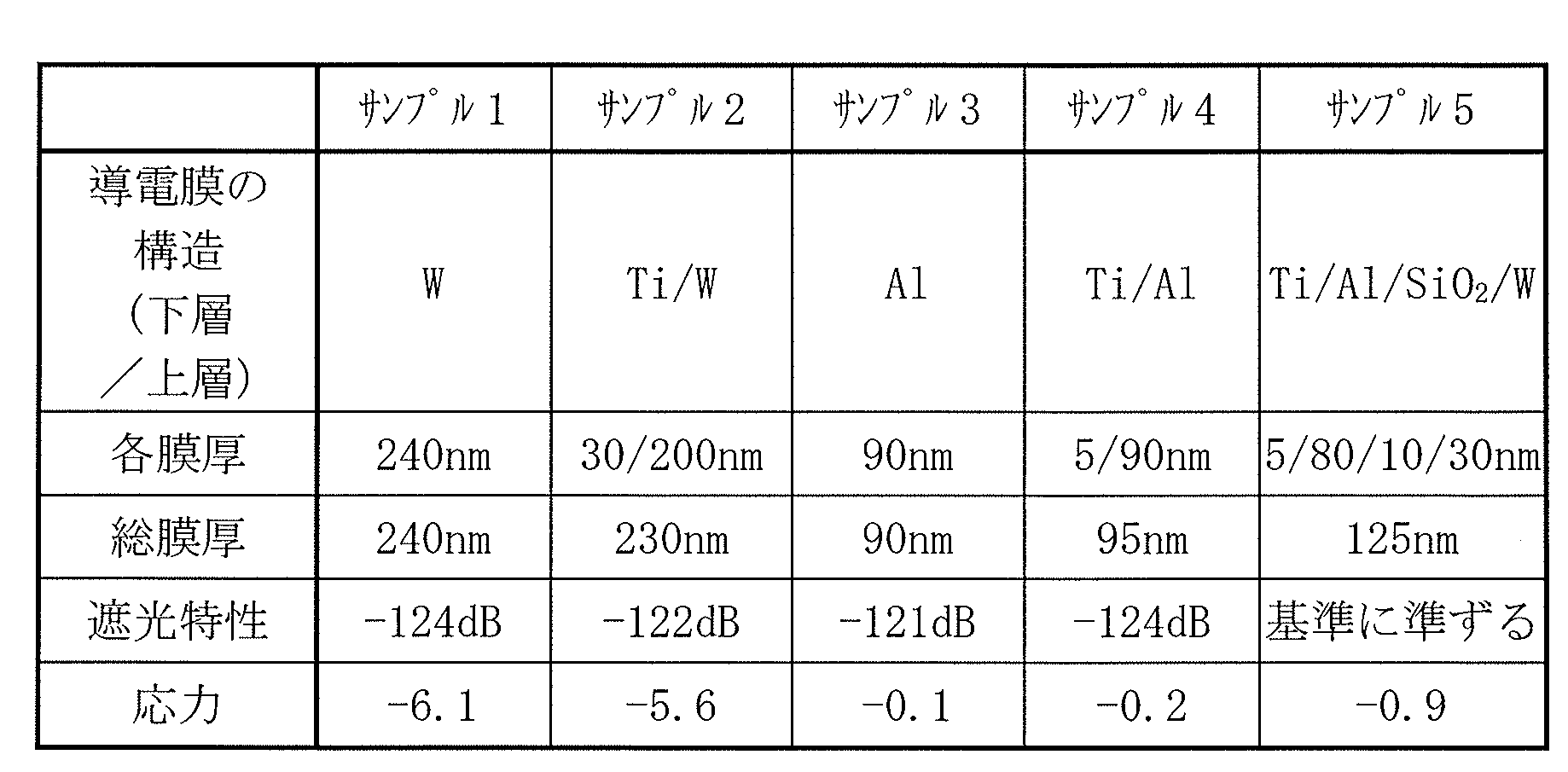
図22は、本開示の第3の実施の形態に係る受光素子(受光素子3)の断面構成を模式的に表したものである。受光素子3は、上記第1の実施の形態と同様に、例えばIII-V族半導体等の化合物半導体材料を用いた赤外線センサ等に適用されるものであり、例えば、可視領域(例えば380nm以上780nm未満)~短赤外領域(例えば780nm以上2400nm未満)の波長の光に、光電変換機能を有するものである。受光素子3は、導電膜15B上に、例えば、ブラックレジストからなる遮光膜37が設けられたものである。
図26は、上記第1~第3の実施の形態の変形例1に係る受光素子(受光素子4)の要部の断面構成を表したものである。この受光素子4は、埋込層18が、積層された第1埋込層18Aおよび第2埋込層18Bを含んでいる。この点を除き、受光素子4は受光素子1と同様の構成および効果を有している。なお、図26では、一例として図1に示した受光素子1を基にした断面構成を表している。また、図26では、簡略化のためパッシベーション膜16A,16Bはまとめてパッシベーション膜16として示している。
図31は、上記第1~第3の実施の形態の変形例2に係る受光素子(受光素子5)の要部の断面構成を表したものである。この受光素子5は、素子基板10の光入射面S1(読出回路基板20との対向面と反対面)にカラーフィルタ層41およびオンチップレンズ(集光レンズ)42を有している。この点を除き、受光素子5は受光素子1と同様の構成および効果を有している。なお、図31では、一例として図1に示した受光素子1を基にした断面構成を表している。また、図31では、簡略化のためパッシベーション膜16A,16Bはまとめてパッシベーション膜16として示している。
図32A~図32Eは、上記第1~第3の実施の形態の変形例3に係る受光素子(図33の受光素子6)の製造工程を工程順に表したものである。この受光素子6は、半導体層10Sを保護するためのキャップ層(図32Aのキャップ層35)を形成した後に、このキャップ層を間にして半導体層10Sを仮基板33に接合し、製造される。この点を除き、受光素子6は、受光素子1と同様の構成を有し、その作用および効果も同様である。なお、図33では、一例として図1に示した受光素子1を基にした断面構成を表している。また、図33では、簡略化のためパッシベーション膜16A,16Bはまとめてパッシベーション膜16として示している。
図37,図38は、上記第2,第3の実施の形態の変形例4に係る受光素子(受光素子7A,7B)の断面構成を模式的に表したものである。この受光素子7A,7Bは、第1コンタクト層52、光電変換層53および第2コンタクト層54が、複数の画素Pに対して共通の半導体層50Sを構成しており、この半導体層50Sの光入射面S1側の隣り合う複数の画素Pの間に、遮光性を有する第2電極55が設けられている。この点を除き、受光素子7A,7Bは、受光素子1と同様の構成を有し、その作用および効果も同様である。
図39は、上記第1~第3の実施の形態の変形例5に係る受光素子(受光素子8)の断面構成を模式的に表したものである。この受光素子8は、化合物半導体材料を含む素子基板10とシリコン(Si)を含む半導体層(半導体層71S、第2半導体層)との積層構造を有している。この点を除き、受光素子8は、受光素子1と同様の構成を有し、その作用および効果も同様である。なお、図39では、一例として図1に示した受光素子1を基にした断面構成を表している。また、図39では、簡略化のためパッシベーション膜16A,16Bはまとめてパッシベーション膜16として示している。
上記実施の形態等において説明した受光素子1(または、受光素子1,2,3,4,5,6,7A,7B,8、以下、まとめて受光素子1という)は、例えば、撮像素子に適用される。この撮像素子は、例えば赤外線イメージセンサである。
上述の撮像素子は、例えば赤外領域を撮像可能なカメラなど、様々なタイプの電子機器に適用することができる。図40に、その一例として、電子機器9(カメラ)の概略構成を示す。この電子機器9は、例えば静止画または動画を撮影可能なカメラであり、受光素子1により構成された撮像素子9Aと、光学系(光学レンズ)310と、シャッタ装置311と、撮像素子9Aおよびシャッタ装置311を駆動する駆動部313と、信号処理部312とを有する。
本開示に係る技術は、様々な製品へ応用することができる。例えば、本開示に係る技術は、内視鏡手術システムに適用されてもよい。
本開示に係る技術は、様々な製品へ応用することができる。例えば、本開示に係る技術は、自動車、電気自動車、ハイブリッド電気自動車、自動二輪車、自転車、パーソナルモビリティ、飛行機、ドローン、船舶、ロボット等のいずれかの種類の移動体に搭載される装置として実現されてもよい。
(1)
配線層と化合物半導体材料を含む第1半導体層とが積層して設けられた素子領域、および前記素子領域の外側の周辺領域を有する素子基板と、
前記配線層を間にして前記第1半導体層に対向し、前記配線層を介して前記第1半導体層に電気的に接続された読出回路基板と、
前記配線層に設けられると共に、前記第1半導体層に電気的に接続された第1電極と、
前記第1半導体層を間にして前記第1電極に対向する第2電極と、
前記第2電極上に設けられると共に、非還元性を有する絶縁層と
を備えた半導体素子。
(2)
前記絶縁層は、酸化物(MxOy)、窒化物(MxNy)および酸窒化物(MxOyNz)のうちのいずれかを含む、前記(1)に記載の半導体素子。
(Mは、ケイ素(Si),チタン(Ti),ハフニウム(Hf),ジルコニウム(Zr)およびイットリウム(Y)のうちのいずれかである。x,y,zは1以上の整数である。)
(3)
前記絶縁層は、2.0g/cm3以上8.0g/cm3以下の膜密度を有する酸化膜によって形成されている、前記(1)または(2)に記載の半導体素子。
(4)
前記絶縁層は多層構造を有する、前記(1)乃至(3)のうちのいずれかに記載の半導体素子。
(5)
前記絶縁層は前記素子領域の前記周辺領域の近傍に開口を有し、
前記周辺領域の近傍において、前記絶縁層の上方に、前記開口を介して前記第2電極と電気的に接続される導電膜をさらに有する、前記(1)乃至(4)のうちのいずれかに記載の半導体素子。
(6)
前記導電膜は、アルミニウム(Al)を用いて形成されている、前記(5)に記載の半導体素子。
(7)
前記開口内において、さらに、前記第2電極と前記導電膜との間にバリアメタルを有する、前記(6)に記載の半導体素子。
(8)
前記導電膜は、前記素子領域の前記周辺領域の近傍から前記周辺領域にかけて設けられている、前記(5)乃至(7)のうちのいずれかに記載の半導体素子。
(9)
前記素子基板は、さらに、前記周辺領域に、前記読出回路基板まで貫通する貫通孔を有し、
前記導電膜は、前記貫通孔を介して前記読出回路基板と電気的に接続されている、前記(5)乃至(8)のうちのいずれかに記載の半導体素子。
(10)
前記導電膜は遮光性を有する、前記(5)乃至(9)のうちのいずれかに記載の半導体素子。
(11)
前記導電膜の上方にブラックレジストからなる遮光膜をさらに有する、前記(5)乃至(10)のうちのいずれかに記載の半導体素子。
(12)
前記遮光膜の前記素子領域側の端面は、前記導電膜の前記素子領域側の端面よりも前記素子領域側に延在している、前記(11)に記載の半導体素子。
(13)
前記素子基板の前記周辺領域は、前記読出回路基板との接合面を有する、前記(1)乃至(12)のうちのいずれかに記載の半導体素子。
(14)
前記素子基板の前記素子領域は、前記周辺領域の前記接合面と同一平面上で、前記読出回路基板に接合されている、前記(13)に記載の半導体素子。
(15)
前記素子基板は、更に、前記周辺領域に前記第1半導体層を囲む埋込層を有する、前記(13)または(14)に記載の半導体素子。
(16)
前記化合物半導体材料は、赤外領域の波長の光を吸収する、前記(1)乃至(15)のうちのいずれかに記載の半導体素子。
(17)
前記化合物半導体材料は、InGaAs,InAsSb,InAs,InSbおよびHgCdTeのうちのいずれか1つである、前記(1)乃至(16)のうちのいずれかに記載の半導体素子。
(18)
更に、前記第1半導体層の前記読出回路基板との対向面とは反対面側に、オンチップレンズを有する、前記(1)乃至(17)のうちのいずれかに記載の半導体素子。
(19)
配線層と化合物半導体材料を含む第1半導体層とが積層して設けられた素子領域、および前記素子領域の外側の周辺領域を有する素子基板と、
前記配線層を間にして前記第1半導体層に対向し、前記配線層を介して前記第1半導体層に電気的に接続された読出回路基板と、
前記配線層に設けられると共に、前記第1半導体層に電気的に接続された第1電極と、
前記第1半導体層を間にして前記第1電極に対向する第2電極と、
前記第2電極上に設けられると共に、前記素子領域の前記周辺領域の近傍に開口を有する絶縁層と、
前記絶縁層の上方に設けられると共に、前記開口を介して前記第2電極と電気的に接続されるアルミニウム(Al)を含む導電膜と
を備えた半導体素子。
(20)
配線層と化合物半導体材料を含む第1半導体層とが積層して設けられた素子領域、および前記素子領域の外側の周辺領域を有する素子基板と、
前記配線層を間にして前記第1半導体層に対向し、前記配線層を介して前記第1半導体層に電気的に接続された読出回路基板と、
前記配線層に設けられると共に、前記第1半導体層に電気的に接続された第1電極と、
前記第1半導体層を間にして前記第1電極に対向する第2電極と、
前記第2電極上に設けられると共に、前記素子領域の前記周辺領域の近傍に開口を有する絶縁層と、
前記絶縁層の上方に設けられると共に、前記開口を介して前記第2電極と電気的に接続される導電膜と、
前記導電膜上に設けられると共に、ブラックレジストからなる遮光膜と
を備えた半導体素子。
Claims (20)
- 配線層と化合物半導体材料を含む第1半導体層とが積層して設けられた素子領域、および前記素子領域の外側の周辺領域を有する素子基板と、
前記配線層を間にして前記第1半導体層に対向し、前記配線層を介して前記第1半導体層に電気的に接続された読出回路基板と、
前記配線層に設けられると共に、前記第1半導体層に電気的に接続された第1電極と、
前記第1半導体層を間にして前記第1電極に対向する第2電極と、
前記第2電極上に設けられると共に、非還元性を有する絶縁層と
を備えた半導体素子。 - 前記絶縁層は、酸化物(MxOy)、窒化物(MxNy)および酸窒化物(MxOyNz)のうちのいずれかを含む、請求項1に記載の半導体素子。
(Mは、ケイ素(Si),チタン(Ti),ハフニウム(Hf),ジルコニウム(Zr)およびイットリウム(Y)のうちのいずれかである。x,y,zは1以上の整数である。) - 前記絶縁層は、2.0g/cm3以上8.0g/cm3以下の膜密度を有する酸化膜によって形成されている、請求項1に記載の半導体素子。
- 前記絶縁層は多層構造を有する、請求項1に記載の半導体素子。
- 前記絶縁層は前記素子領域の前記周辺領域の近傍に開口を有し、
前記周辺領域の近傍において、前記絶縁層の上方に、前記開口を介して前記第2電極と電気的に接続される導電膜をさらに有する、請求項1に記載の半導体素子。 - 前記導電膜は、アルミニウム(Al)を用いて形成されている、請求項5に記載の半導体素子。
- 前記開口内において、さらに、前記第2電極と前記導電膜との間にバリアメタルを有する、請求項6に記載の半導体素子。
- 前記導電膜は、前記素子領域の前記周辺領域の近傍から前記周辺領域にかけて設けられている、請求項5に記載の半導体素子。
- 前記素子基板は、さらに、前記周辺領域に、前記読出回路基板まで貫通する貫通孔を有し、
前記導電膜は、前記貫通孔を介して前記読出回路基板と電気的に接続されている、請求項5に記載の半導体素子。 - 前記導電膜は遮光性を有する、請求項5に記載の半導体素子。
- 前記導電膜の上方にブラックレジストからなる遮光膜をさらに有する、請求項5に記載の半導体素子。
- 前記遮光膜の前記素子領域側の端面は、前記導電膜の前記素子領域側の端面よりも前記素子領域側に延在している、請求項11に記載の半導体素子。
- 前記素子基板の前記周辺領域は、前記読出回路基板との接合面を有する、請求項1に記載の半導体素子。
- 前記素子基板の前記素子領域は、前記周辺領域の前記接合面と同一平面上で、前記読出回路基板に接合されている、請求項13に記載の半導体素子。
- 前記素子基板は、更に、前記周辺領域に前記第1半導体層を囲む埋込層を有する、請求項13に記載の半導体素子。
- 前記化合物半導体材料は、赤外領域の波長の光を吸収する、請求項1に記載の半導体素子。
- 前記化合物半導体材料は、InGaAs,InAsSb,InAs,InSbおよびHgCdTeのうちのいずれか1つである、請求項1に記載の半導体素子。
- 更に、前記第1半導体層の前記読出回路基板との対向面とは反対面側に、オンチップレンズを有する、請求項1に記載の半導体素子。
- 配線層と化合物半導体材料を含む第1半導体層とが積層して設けられた素子領域、および前記素子領域の外側の周辺領域を有する素子基板と、
前記配線層を間にして前記第1半導体層に対向し、前記配線層を介して前記第1半導体層に電気的に接続された読出回路基板と、
前記配線層に設けられると共に、前記第1半導体層に電気的に接続された第1電極と、
前記第1半導体層を間にして前記第1電極に対向する第2電極と、
前記第2電極上に設けられると共に、前記素子領域の前記周辺領域の近傍に開口を有する絶縁層と、
前記絶縁層の上方に設けられると共に、前記開口を介して前記第2電極と電気的に接続されるアルミニウム(Al)を含む導電膜と
を備えた半導体素子。 - 配線層と化合物半導体材料を含む第1半導体層とが積層して設けられた素子領域、および前記素子領域の外側の周辺領域を有する素子基板と、
前記配線層を間にして前記第1半導体層に対向し、前記配線層を介して前記第1半導体層に電気的に接続された読出回路基板と、
前記配線層に設けられると共に、前記第1半導体層に電気的に接続された第1電極と、
前記第1半導体層を間にして前記第1電極に対向する第2電極と、
前記第2電極上に設けられると共に、前記素子領域の前記周辺領域の近傍に開口を有する絶縁層と、
前記絶縁層の上方に設けられると共に、前記開口を介して前記第2電極と電気的に接続される導電膜と、
前記導電膜上に設けられると共に、ブラックレジストからなる遮光膜と
を備えた半導体素子。
Priority Applications (3)
| Application Number | Priority Date | Filing Date | Title |
|---|---|---|---|
| CN201980073680.0A CN113039652B (zh) | 2018-12-27 | 2019-11-22 | 半导体元件 |
| US17/415,119 US12154929B2 (en) | 2018-12-27 | 2019-11-22 | Semiconductor element |
| JP2020562934A JP7634991B2 (ja) | 2018-12-27 | 2019-11-22 | 半導体素子 |
Applications Claiming Priority (2)
| Application Number | Priority Date | Filing Date | Title |
|---|---|---|---|
| JP2018245180 | 2018-12-27 | ||
| JP2018-245180 | 2018-12-27 |
Publications (1)
| Publication Number | Publication Date |
|---|---|
| WO2020137283A1 true WO2020137283A1 (ja) | 2020-07-02 |
Family
ID=71129008
Family Applications (1)
| Application Number | Title | Priority Date | Filing Date |
|---|---|---|---|
| PCT/JP2019/045726 Ceased WO2020137283A1 (ja) | 2018-12-27 | 2019-11-22 | 半導体素子 |
Country Status (5)
| Country | Link |
|---|---|
| US (1) | US12154929B2 (ja) |
| JP (1) | JP7634991B2 (ja) |
| CN (1) | CN113039652B (ja) |
| TW (1) | TWI850281B (ja) |
| WO (1) | WO2020137283A1 (ja) |
Cited By (2)
| Publication number | Priority date | Publication date | Assignee | Title |
|---|---|---|---|---|
| JPWO2022265059A1 (ja) * | 2021-06-16 | 2022-12-22 | ||
| WO2023074136A1 (ja) * | 2021-10-26 | 2023-05-04 | ソニーセミコンダクタソリューションズ株式会社 | 半導体装置、機器及び半導体装置の製造方法 |
Families Citing this family (8)
| Publication number | Priority date | Publication date | Assignee | Title |
|---|---|---|---|---|
| JP2021180211A (ja) * | 2020-05-11 | 2021-11-18 | パナソニックIpマネジメント株式会社 | 撮像装置 |
| US11991824B2 (en) | 2020-08-28 | 2024-05-21 | Unimicron Technology Corp. | Circuit board structure and manufacturing method thereof |
| US11894477B2 (en) * | 2021-05-17 | 2024-02-06 | Raytheon Company | Electrical device with stress buffer layer and stress compensation layer |
| CN115513274B (zh) * | 2021-06-07 | 2025-12-23 | 联华电子股份有限公司 | 避免翘曲的半导体结构及其制作方法 |
| CN115602688A (zh) * | 2021-07-09 | 2023-01-13 | 欣兴电子股份有限公司(Tw) | 异质基板结构及其制作方法 |
| JP2023043671A (ja) * | 2021-09-16 | 2023-03-29 | キオクシア株式会社 | 半導体記憶装置及びその設計方法 |
| JP2024006789A (ja) * | 2022-07-04 | 2024-01-17 | キオクシア株式会社 | 半導体装置及び半導体装置の製造方法 |
| TWI849904B (zh) * | 2023-05-15 | 2024-07-21 | 友達光電股份有限公司 | 元件基板及其製造方法 |
Citations (3)
| Publication number | Priority date | Publication date | Assignee | Title |
|---|---|---|---|---|
| US20080067622A1 (en) * | 2006-09-15 | 2008-03-20 | Peter Steven Bui | High density photodiodes |
| JP2017022313A (ja) * | 2015-07-14 | 2017-01-26 | 株式会社東芝 | カメラモジュール |
| WO2018194030A1 (ja) * | 2017-04-19 | 2018-10-25 | ソニーセミコンダクタソリューションズ株式会社 | 半導体素子およびその製造方法、並びに電子機器 |
Family Cites Families (9)
| Publication number | Priority date | Publication date | Assignee | Title |
|---|---|---|---|---|
| TW548860B (en) * | 2001-06-20 | 2003-08-21 | Semiconductor Energy Lab | Light emitting device and method of manufacturing the same |
| US20100224878A1 (en) * | 2009-03-05 | 2010-09-09 | Semiconductor Energy Laboratory Co., Ltd. | Semiconductor device |
| JP5442394B2 (ja) * | 2009-10-29 | 2014-03-12 | ソニー株式会社 | 固体撮像装置とその製造方法、及び電子機器 |
| JP2012094720A (ja) * | 2010-10-27 | 2012-05-17 | Sony Corp | 固体撮像装置、半導体装置、固体撮像装置の製造方法、半導体装置の製造方法、及び電子機器 |
| JP5921129B2 (ja) * | 2011-02-09 | 2016-05-24 | キヤノン株式会社 | 固体撮像装置、及び固体撮像装置の製造方法 |
| JP2012238648A (ja) * | 2011-05-10 | 2012-12-06 | Sony Corp | 固体撮像装置及び電子機器 |
| TWI495041B (zh) * | 2011-07-05 | 2015-08-01 | 新力股份有限公司 | 半導體裝置、用於半導體裝置之製造方法及電子設備 |
| FR2977982B1 (fr) | 2011-07-11 | 2014-06-20 | New Imaging Technologies Sas | Matrice de photodiodes ingaas |
| TW201637190A (zh) * | 2015-03-25 | 2016-10-16 | 新力股份有限公司 | 固體攝像裝置及電子機器 |
-
2019
- 2019-11-19 TW TW108141892A patent/TWI850281B/zh active
- 2019-11-22 CN CN201980073680.0A patent/CN113039652B/zh active Active
- 2019-11-22 US US17/415,119 patent/US12154929B2/en active Active
- 2019-11-22 WO PCT/JP2019/045726 patent/WO2020137283A1/ja not_active Ceased
- 2019-11-22 JP JP2020562934A patent/JP7634991B2/ja active Active
Patent Citations (3)
| Publication number | Priority date | Publication date | Assignee | Title |
|---|---|---|---|---|
| US20080067622A1 (en) * | 2006-09-15 | 2008-03-20 | Peter Steven Bui | High density photodiodes |
| JP2017022313A (ja) * | 2015-07-14 | 2017-01-26 | 株式会社東芝 | カメラモジュール |
| WO2018194030A1 (ja) * | 2017-04-19 | 2018-10-25 | ソニーセミコンダクタソリューションズ株式会社 | 半導体素子およびその製造方法、並びに電子機器 |
Cited By (3)
| Publication number | Priority date | Publication date | Assignee | Title |
|---|---|---|---|---|
| JPWO2022265059A1 (ja) * | 2021-06-16 | 2022-12-22 | ||
| WO2022265059A1 (ja) * | 2021-06-16 | 2022-12-22 | ソニーセミコンダクタソリューションズ株式会社 | 光検出装置、光検出装置の製造方法、及び電子機器 |
| WO2023074136A1 (ja) * | 2021-10-26 | 2023-05-04 | ソニーセミコンダクタソリューションズ株式会社 | 半導体装置、機器及び半導体装置の製造方法 |
Also Published As
| Publication number | Publication date |
|---|---|
| JPWO2020137283A1 (ja) | 2021-11-11 |
| TWI850281B (zh) | 2024-08-01 |
| CN113039652B (zh) | 2025-02-25 |
| US20220052099A1 (en) | 2022-02-17 |
| CN113039652A (zh) | 2021-06-25 |
| JP7634991B2 (ja) | 2025-02-25 |
| TW202101732A (zh) | 2021-01-01 |
| US12154929B2 (en) | 2024-11-26 |
Similar Documents
| Publication | Publication Date | Title |
|---|---|---|
| JP7631384B2 (ja) | 半導体素子および電子機器 | |
| JP7634991B2 (ja) | 半導体素子 | |
| JP7660642B2 (ja) | 半導体素子 | |
| US12484329B2 (en) | Semiconductor element and electronic apparatus | |
| JP7524160B2 (ja) | 受光素子の製造方法 | |
| US20230014646A1 (en) | Semiconductor element and electronic apparatus | |
| WO2020137282A1 (ja) | 撮像素子および電子機器 | |
| JP7653788B2 (ja) | 撮像素子および電子機器 |
Legal Events
| Date | Code | Title | Description |
|---|---|---|---|
| 121 | Ep: the epo has been informed by wipo that ep was designated in this application |
Ref document number: 19904946 Country of ref document: EP Kind code of ref document: A1 |
|
| ENP | Entry into the national phase |
Ref document number: 2020562934 Country of ref document: JP Kind code of ref document: A |
|
| NENP | Non-entry into the national phase |
Ref country code: DE |
|
| 122 | Ep: pct application non-entry in european phase |
Ref document number: 19904946 Country of ref document: EP Kind code of ref document: A1 |
|
| WWG | Wipo information: grant in national office |
Ref document number: 201980073680.0 Country of ref document: CN |