WO2020129237A1 - 3次元半導体装置の製造方法 - Google Patents
3次元半導体装置の製造方法 Download PDFInfo
- Publication number
- WO2020129237A1 WO2020129237A1 PCT/JP2018/047245 JP2018047245W WO2020129237A1 WO 2020129237 A1 WO2020129237 A1 WO 2020129237A1 JP 2018047245 W JP2018047245 W JP 2018047245W WO 2020129237 A1 WO2020129237 A1 WO 2020129237A1
- Authority
- WO
- WIPO (PCT)
- Prior art keywords
- material layer
- strip
- layer
- shaped material
- shaped
- Prior art date
- Legal status (The legal status is an assumption and is not a legal conclusion. Google has not performed a legal analysis and makes no representation as to the accuracy of the status listed.)
- Ceased
Links
Images























Classifications
-
- H—ELECTRICITY
- H10—SEMICONDUCTOR DEVICES; ELECTRIC SOLID-STATE DEVICES NOT OTHERWISE PROVIDED FOR
- H10D—INORGANIC ELECTRIC SEMICONDUCTOR DEVICES
- H10D84/00—Integrated devices formed in or on semiconductor substrates that comprise only semiconducting layers, e.g. on Si wafers or on GaAs-on-Si wafers
- H10D84/01—Manufacture or treatment
- H10D84/0123—Integrating together multiple components covered by H10D12/00 or H10D30/00, e.g. integrating multiple IGBTs
- H10D84/0126—Integrating together multiple components covered by H10D12/00 or H10D30/00, e.g. integrating multiple IGBTs the components including insulated gates, e.g. IGFETs
- H10D84/0165—Integrating together multiple components covered by H10D12/00 or H10D30/00, e.g. integrating multiple IGBTs the components including insulated gates, e.g. IGFETs the components including complementary IGFETs, e.g. CMOS devices
- H10D84/0195—Integrating together multiple components covered by H10D12/00 or H10D30/00, e.g. integrating multiple IGBTs the components including insulated gates, e.g. IGFETs the components including complementary IGFETs, e.g. CMOS devices the components including vertical IGFETs
-
- H—ELECTRICITY
- H10—SEMICONDUCTOR DEVICES; ELECTRIC SOLID-STATE DEVICES NOT OTHERWISE PROVIDED FOR
- H10P—GENERIC PROCESSES OR APPARATUS FOR THE MANUFACTURE OR TREATMENT OF DEVICES COVERED BY CLASS H10
- H10P76/00—Manufacture or treatment of masks on semiconductor bodies, e.g. by lithography or photolithography
- H10P76/40—Manufacture or treatment of masks on semiconductor bodies, e.g. by lithography or photolithography of masks comprising inorganic materials
- H10P76/408—Manufacture or treatment of masks on semiconductor bodies, e.g. by lithography or photolithography of masks comprising inorganic materials characterised by their sizes, orientations, dispositions, behaviours or shapes
- H10P76/4088—Processes for improving the resolution of the masks
-
- H—ELECTRICITY
- H10—SEMICONDUCTOR DEVICES; ELECTRIC SOLID-STATE DEVICES NOT OTHERWISE PROVIDED FOR
- H10B—ELECTRONIC MEMORY DEVICES
- H10B10/00—Static random access memory [SRAM] devices
- H10B10/12—Static random access memory [SRAM] devices comprising a MOSFET load element
-
- H—ELECTRICITY
- H10—SEMICONDUCTOR DEVICES; ELECTRIC SOLID-STATE DEVICES NOT OTHERWISE PROVIDED FOR
- H10D—INORGANIC ELECTRIC SEMICONDUCTOR DEVICES
- H10D30/00—Field-effect transistors [FET]
- H10D30/01—Manufacture or treatment
- H10D30/014—Manufacture or treatment of FETs having zero-dimensional [0D] or one-dimensional [1D] channels, e.g. quantum wire FETs, single-electron transistors [SET] or Coulomb blockade transistors
-
- H—ELECTRICITY
- H10—SEMICONDUCTOR DEVICES; ELECTRIC SOLID-STATE DEVICES NOT OTHERWISE PROVIDED FOR
- H10D—INORGANIC ELECTRIC SEMICONDUCTOR DEVICES
- H10D30/00—Field-effect transistors [FET]
- H10D30/01—Manufacture or treatment
- H10D30/021—Manufacture or treatment of FETs having insulated gates [IGFET]
- H10D30/025—Manufacture or treatment of FETs having insulated gates [IGFET] of vertical IGFETs
-
- H—ELECTRICITY
- H10—SEMICONDUCTOR DEVICES; ELECTRIC SOLID-STATE DEVICES NOT OTHERWISE PROVIDED FOR
- H10D—INORGANIC ELECTRIC SEMICONDUCTOR DEVICES
- H10D30/00—Field-effect transistors [FET]
- H10D30/40—FETs having zero-dimensional [0D], one-dimensional [1D] or two-dimensional [2D] charge carrier gas channels
- H10D30/43—FETs having zero-dimensional [0D], one-dimensional [1D] or two-dimensional [2D] charge carrier gas channels having one-dimensional [1D] charge carrier gas channels, e.g. quantum wire FETs or transistors having 1D quantum-confined channels
-
- H—ELECTRICITY
- H10—SEMICONDUCTOR DEVICES; ELECTRIC SOLID-STATE DEVICES NOT OTHERWISE PROVIDED FOR
- H10D—INORGANIC ELECTRIC SEMICONDUCTOR DEVICES
- H10D30/00—Field-effect transistors [FET]
- H10D30/60—Insulated-gate field-effect transistors [IGFET]
- H10D30/63—Vertical IGFETs
-
- H—ELECTRICITY
- H10—SEMICONDUCTOR DEVICES; ELECTRIC SOLID-STATE DEVICES NOT OTHERWISE PROVIDED FOR
- H10D—INORGANIC ELECTRIC SEMICONDUCTOR DEVICES
- H10D30/00—Field-effect transistors [FET]
- H10D30/60—Insulated-gate field-effect transistors [IGFET]
- H10D30/67—Thin-film transistors [TFT]
- H10D30/6729—Thin-film transistors [TFT] characterised by the electrodes
- H10D30/673—Thin-film transistors [TFT] characterised by the electrodes characterised by the shapes, relative sizes or dispositions of the gate electrodes
- H10D30/6735—Thin-film transistors [TFT] characterised by the electrodes characterised by the shapes, relative sizes or dispositions of the gate electrodes having gates fully surrounding the channels, e.g. gate-all-around
-
- H—ELECTRICITY
- H10—SEMICONDUCTOR DEVICES; ELECTRIC SOLID-STATE DEVICES NOT OTHERWISE PROVIDED FOR
- H10D—INORGANIC ELECTRIC SEMICONDUCTOR DEVICES
- H10D62/00—Semiconductor bodies, or regions thereof, of devices having potential barriers
- H10D62/10—Shapes, relative sizes or dispositions of the regions of the semiconductor bodies; Shapes of the semiconductor bodies
- H10D62/117—Shapes of semiconductor bodies
- H10D62/118—Nanostructure semiconductor bodies
- H10D62/119—Nanowire, nanosheet or nanotube semiconductor bodies
- H10D62/121—Nanowire, nanosheet or nanotube semiconductor bodies oriented parallel to substrates
-
- H—ELECTRICITY
- H10—SEMICONDUCTOR DEVICES; ELECTRIC SOLID-STATE DEVICES NOT OTHERWISE PROVIDED FOR
- H10D—INORGANIC ELECTRIC SEMICONDUCTOR DEVICES
- H10D62/00—Semiconductor bodies, or regions thereof, of devices having potential barriers
- H10D62/10—Shapes, relative sizes or dispositions of the regions of the semiconductor bodies; Shapes of the semiconductor bodies
- H10D62/117—Shapes of semiconductor bodies
- H10D62/118—Nanostructure semiconductor bodies
- H10D62/119—Nanowire, nanosheet or nanotube semiconductor bodies
- H10D62/122—Nanowire, nanosheet or nanotube semiconductor bodies oriented at angles to substrates, e.g. perpendicular to substrates
-
- H—ELECTRICITY
- H10—SEMICONDUCTOR DEVICES; ELECTRIC SOLID-STATE DEVICES NOT OTHERWISE PROVIDED FOR
- H10D—INORGANIC ELECTRIC SEMICONDUCTOR DEVICES
- H10D84/00—Integrated devices formed in or on semiconductor substrates that comprise only semiconducting layers, e.g. on Si wafers or on GaAs-on-Si wafers
- H10D84/01—Manufacture or treatment
- H10D84/0123—Integrating together multiple components covered by H10D12/00 or H10D30/00, e.g. integrating multiple IGBTs
- H10D84/0126—Integrating together multiple components covered by H10D12/00 or H10D30/00, e.g. integrating multiple IGBTs the components including insulated gates, e.g. IGFETs
- H10D84/0165—Integrating together multiple components covered by H10D12/00 or H10D30/00, e.g. integrating multiple IGBTs the components including insulated gates, e.g. IGFETs the components including complementary IGFETs, e.g. CMOS devices
- H10D84/0167—Manufacturing their channels
-
- H—ELECTRICITY
- H10—SEMICONDUCTOR DEVICES; ELECTRIC SOLID-STATE DEVICES NOT OTHERWISE PROVIDED FOR
- H10D—INORGANIC ELECTRIC SEMICONDUCTOR DEVICES
- H10D84/00—Integrated devices formed in or on semiconductor substrates that comprise only semiconducting layers, e.g. on Si wafers or on GaAs-on-Si wafers
- H10D84/01—Manufacture or treatment
- H10D84/02—Manufacture or treatment characterised by using material-based technologies
- H10D84/03—Manufacture or treatment characterised by using material-based technologies using Group IV technology, e.g. silicon technology or silicon-carbide [SiC] technology
- H10D84/038—Manufacture or treatment characterised by using material-based technologies using Group IV technology, e.g. silicon technology or silicon-carbide [SiC] technology using silicon technology, e.g. SiGe
-
- H—ELECTRICITY
- H10—SEMICONDUCTOR DEVICES; ELECTRIC SOLID-STATE DEVICES NOT OTHERWISE PROVIDED FOR
- H10D—INORGANIC ELECTRIC SEMICONDUCTOR DEVICES
- H10D84/00—Integrated devices formed in or on semiconductor substrates that comprise only semiconducting layers, e.g. on Si wafers or on GaAs-on-Si wafers
- H10D84/80—Integrated devices formed in or on semiconductor substrates that comprise only semiconducting layers, e.g. on Si wafers or on GaAs-on-Si wafers characterised by the integration of at least one component covered by groups H10D12/00 or H10D30/00, e.g. integration of IGFETs
- H10D84/82—Integrated devices formed in or on semiconductor substrates that comprise only semiconducting layers, e.g. on Si wafers or on GaAs-on-Si wafers characterised by the integration of at least one component covered by groups H10D12/00 or H10D30/00, e.g. integration of IGFETs of only field-effect components
- H10D84/83—Integrated devices formed in or on semiconductor substrates that comprise only semiconducting layers, e.g. on Si wafers or on GaAs-on-Si wafers characterised by the integration of at least one component covered by groups H10D12/00 or H10D30/00, e.g. integration of IGFETs of only field-effect components of only insulated-gate FETs [IGFET]
- H10D84/85—Complementary IGFETs, e.g. CMOS
-
- H—ELECTRICITY
- H10—SEMICONDUCTOR DEVICES; ELECTRIC SOLID-STATE DEVICES NOT OTHERWISE PROVIDED FOR
- H10P—GENERIC PROCESSES OR APPARATUS FOR THE MANUFACTURE OR TREATMENT OF DEVICES COVERED BY CLASS H10
- H10P76/00—Manufacture or treatment of masks on semiconductor bodies, e.g. by lithography or photolithography
- H10P76/40—Manufacture or treatment of masks on semiconductor bodies, e.g. by lithography or photolithography of masks comprising inorganic materials
- H10P76/408—Manufacture or treatment of masks on semiconductor bodies, e.g. by lithography or photolithography of masks comprising inorganic materials characterised by their sizes, orientations, dispositions, behaviours or shapes
- H10P76/4083—Manufacture or treatment of masks on semiconductor bodies, e.g. by lithography or photolithography of masks comprising inorganic materials characterised by their sizes, orientations, dispositions, behaviours or shapes characterised by their behaviours during the lithography processes, e.g. soluble masks or redeposited masks
-
- H—ELECTRICITY
- H10—SEMICONDUCTOR DEVICES; ELECTRIC SOLID-STATE DEVICES NOT OTHERWISE PROVIDED FOR
- H10P—GENERIC PROCESSES OR APPARATUS FOR THE MANUFACTURE OR TREATMENT OF DEVICES COVERED BY CLASS H10
- H10P76/00—Manufacture or treatment of masks on semiconductor bodies, e.g. by lithography or photolithography
- H10P76/40—Manufacture or treatment of masks on semiconductor bodies, e.g. by lithography or photolithography of masks comprising inorganic materials
- H10P76/408—Manufacture or treatment of masks on semiconductor bodies, e.g. by lithography or photolithography of masks comprising inorganic materials characterised by their sizes, orientations, dispositions, behaviours or shapes
- H10P76/4085—Manufacture or treatment of masks on semiconductor bodies, e.g. by lithography or photolithography of masks comprising inorganic materials characterised by their sizes, orientations, dispositions, behaviours or shapes characterised by the processes involved to create the masks
-
- B—PERFORMING OPERATIONS; TRANSPORTING
- B82—NANOTECHNOLOGY
- B82Y—SPECIFIC USES OR APPLICATIONS OF NANOSTRUCTURES; MEASUREMENT OR ANALYSIS OF NANOSTRUCTURES; MANUFACTURE OR TREATMENT OF NANOSTRUCTURES
- B82Y10/00—Nanotechnology for information processing, storage or transmission, e.g. quantum computing or single electron logic
-
- H—ELECTRICITY
- H10—SEMICONDUCTOR DEVICES; ELECTRIC SOLID-STATE DEVICES NOT OTHERWISE PROVIDED FOR
- H10D—INORGANIC ELECTRIC SEMICONDUCTOR DEVICES
- H10D30/00—Field-effect transistors [FET]
- H10D30/60—Insulated-gate field-effect transistors [IGFET]
- H10D30/62—Fin field-effect transistors [FinFET]
-
- H—ELECTRICITY
- H10—SEMICONDUCTOR DEVICES; ELECTRIC SOLID-STATE DEVICES NOT OTHERWISE PROVIDED FOR
- H10D—INORGANIC ELECTRIC SEMICONDUCTOR DEVICES
- H10D30/00—Field-effect transistors [FET]
- H10D30/60—Insulated-gate field-effect transistors [IGFET]
- H10D30/67—Thin-film transistors [TFT]
- H10D30/6728—Vertical TFTs
-
- H—ELECTRICITY
- H10—SEMICONDUCTOR DEVICES; ELECTRIC SOLID-STATE DEVICES NOT OTHERWISE PROVIDED FOR
- H10D—INORGANIC ELECTRIC SEMICONDUCTOR DEVICES
- H10D30/00—Field-effect transistors [FET]
- H10D30/60—Insulated-gate field-effect transistors [IGFET]
- H10D30/67—Thin-film transistors [TFT]
- H10D30/6757—Thin-film transistors [TFT] characterised by the structure of the channel, e.g. transverse or longitudinal shape or doping profile
Definitions
- the present invention relates to a method for manufacturing a three-dimensional semiconductor device.
- the channel In a normal planar MOS transistor, the channel extends horizontally along the upper surface of the semiconductor substrate.
- the channel of the SGT extends in the direction perpendicular to the upper surface of the semiconductor substrate (see, for example, Patent Document 1 and Non-Patent Document 1). Therefore, the SGT can increase the density of the semiconductor device as compared with the planar type MOS transistor.
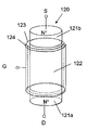
- FIG. 10 shows a schematic structural diagram of the N-channel SGT.
- P-type or i-type (intrinsic) conductivity type Si pillars 120 (hereinafter, the silicon semiconductor pillars are referred to as “Si pillars”) are positioned above and below, and when one is a source, the other is a drain.
- N + layers 121a and 121b (hereinafter, a semiconductor region containing a high concentration of donor impurities is referred to as “N + layer”) are formed.
- the portion of the Si pillar 120 between the N + layers 121a and 121b that will be the source and drain serves as the channel region 122.
- a gate insulating layer 123 is formed so as to surround the channel region 122.
- a gate conductor layer 124 is formed so as to surround the gate insulating layer 123.
- N + layers 121a and 121b serving as sources and drains, a channel region 122, a gate insulating layer 123, and a gate conductor layer 124 are formed in a columnar shape as a whole. Therefore, in plan view, the occupied area of the SGT corresponds to the occupied area of a single source or drain N + layer of the planar MOS transistor. Therefore, the circuit chip having the SGT can realize a further reduction in chip size as compared with the circuit chip having the planar MOS transistor.
- a method for manufacturing a three-dimensional semiconductor device Forming a first material layer on a second substrate that is at least partially or wholly made of a semiconductor layer on the first substrate; Forming a second band-shaped material layer having a first band-shaped material layer extending in one direction in plan view and having the same plan-view shape on the top of the first material layer, Covering the whole and forming a second material layer and a third material layer from the bottom, Smoothing the upper surface positions of the second material layer and the third material layer to the upper surface position of the first strip-shaped material layer; A third strip-shaped material layer sandwiched between side surfaces of the smoothed third material layer and the first strip-shaped material layer is formed on the top of the smoothed second material layer.
- Process Removing the smoothed third material layer; A fourth layer, which is in contact with both side surfaces of the second band-shaped material layer, by etching the second material layer using the first band-shaped material layer and the third band-shaped material layer as a mask. Forming a strip-shaped material layer of Covering the whole and forming a fourth material layer and a fifth material layer from the bottom, Smoothing so that the upper surface positions of the fourth material layer and the fifth material layer are the upper surface positions of the first strip-shaped material layer; A fifth strip-shaped material layer sandwiched between side faces of the smoothed fifth material layer and the third strip-shaped material layer is formed on the top of the smoothed fourth material layer.
- the fourth band-shaped material layer is etched by using the first band-shaped material layer, the third band-shaped material layer, and the fifth band-shaped material layer as a mask to etch the fourth material layer.
- a seventh strip-shaped material layer composed of a single layer or a plurality of layers, which is orthogonal to the first strip-shaped material layer in a plan view, is formed above or below the first strip-shaped material layer,
- the seventh strip-shaped material layer, the second strip-shaped material layer, and the sixth strip-shaped material layer are in a first overlapping region and have a rectangular or circular shape in a plan view.
- first mask material layer with at least the first material layer, the second strip-shaped material layer, or the sixth strip-shaped material layer as a matrix; Etching the second substrate using the first mask material layer as a mask to form a three-dimensional semiconductor layer made of the semiconductor layer on the first substrate,
- the three-dimensionally shaped semiconductor layer is used as a channel, Characterize that.
- the manufacturing method In the step of forming the third strip-shaped material layer, Etching the top of the second material layer using the first strip-shaped material layer and the smoothed third material layer as a mask to form a first recess; Filling the first recess and forming the third strip-shaped material layer whose upper surface position is the same as the upper surface position of the first strip-shaped material layer. Is desirable.
- the manufacturing method In the step of forming the fifth strip-shaped material layer, Using the first strip-shaped material layer, the third strip-shaped material layer, and the fifth material layer as a mask, the top of the fourth material layer is etched to form a second recess. The process of Filling the second recess and forming the fifth strip-shaped material layer whose upper surface position is the same as the upper surface position of the first strip-shaped material layer. Is desirable.
- an eighth strip-shaped material layer extending in one direction is provided on the top thereof, and the seventh strip-shaped material is provided.
- a ninth strip-shaped material layer having the same shape as the layer in plan view is formed, The seventh strip-shaped material layer, Covering the whole and forming a sixth material layer and a seventh material layer from the bottom, Smoothing so that the upper surface positions of the sixth material layer and the seventh material layer are the upper surface positions of the eighth strip-shaped material layer;
- the eighth strip-shaped material layer and the smoothed seventh material layer as a mask, the top of the smoothed sixth material layer is etched to form a third recess.
- Forming a strip-shaped material layer of The remaining strip-shaped material is obtained by removing the eighth strip-shaped material layer and the ninth strip-shaped material layer, or by removing the tenth strip-shaped material layer and the eleventh strip-shaped material layer. It is desirable that the lower layer of the layer or both upper and lower layers be the seventh strip-shaped material layer.
- one of the width of the second strip-shaped material layer and the width of the fourth strip-shaped material layer is formed to be larger than the width of the other. Is desirable.
- one of the second strip-shaped material layer and the sixth strip-shaped material layer is formed to have a width larger than the other width. Is desirable.
- the manufacturing method The three-dimensionally shaped semiconductor layer is a semiconductor pillar that stands vertically on the first substrate, Is desirable.
- the semiconductor pillar includes at least a first semiconductor pillar, a second semiconductor pillar, and a third semiconductor pillar, which are adjacent to each other in the one direction or in a direction orthogonal to the one direction.
- a step of forming a first gate conductor layer surrounding the first gate insulating layer, The first gate conductor layer is formed by filling a space between at least two semiconductor pillars of the first semiconductor pillar, the second semiconductor pillar, and the third semiconductor pillar. Is desirable.
- the manufacturing method A step of removing one of the plurality of semiconductor pillars formed on the substrate, Is desirable.
- the manufacturing method Before forming the plurality of semiconductor pillars, a step of not forming a partial region of the seventh strip-shaped material layer in plan view is included, In a plan view, one of the plurality of semiconductor pillars is not formed below the partial region of the seventh strip-shaped material layer, Is desirable.
- the manufacturing method Oxidizing the smoothed top of the second layer of material to form the third layer of strip material; Is desirable.
- Atomic ions are ion-implanted on the top of the smoothed second material layer to form the third strip-shaped material layer, Is desirable.
- both ends of one side of the second substrate are in contact with the holding material layer, and in the vertical direction, the first semiconductor layer and the eighth material layer are set as a set and are stacked above one another.
- Forming with a different structure Removing the eighth material layer after forming the three-dimensional semiconductor layer; Forming a second gate insulating layer surrounding the first semiconductor layer of the three-dimensionally shaped semiconductor layer; Forming a second gate conductor layer surrounding the second gate insulating layer; Removing the retaining material layer, A step of forming an impurity layer containing a donor or acceptor impurity in contact with both ends of the first semiconductor layer in the one direction in the plan view. Is desirable.
- a method for manufacturing a three-dimensional semiconductor device Forming a first material layer on a second substrate that is at least partially or wholly formed of a semiconductor layer on the first substrate; Forming a second band-shaped material layer having a first band-shaped material layer extending in one direction in plan view and having the same plan-view shape on the top of the first material layer, Covering the whole and forming a second material layer and a third material layer from the bottom, Smoothing the upper surface positions of the second material layer and the third material layer to the upper surface position of the first strip-shaped material layer; A third strip-shaped material layer sandwiched between side surfaces of the smoothed third material layer and the first strip-shaped material layer is formed on the top of the smoothed third material layer.
- a fifth strip-shaped material layer consisting of a single layer or a plurality of layers, which is orthogonal to the fourth strip-shaped material layer in a plan view, is formed above or below the third strip-shaped material layer,
- the first mask material layer having a rectangular or circular shape in plan view in a first overlapping region of the fourth band-shaped material layer and the fifth band-shaped material layer in plan view, Forming a first material layer, the fourth strip-shaped material layer, or the fifth strip-shaped material layer as a matrix, Etching the second substrate using the first mask material layer as a mask to form a three-dimensional semiconductor layer made of the semiconductor layer on the substrate, The three-dimensionally
- the manufacturing method In the step of forming the third strip-shaped material layer, Forming a first recess by etching the top of the second material layer using the first strip-shaped material layer and the third material layer as a mask; Filling the first recess and forming the third strip-shaped material layer whose upper surface position is the same as the upper surface position of the first strip-shaped material layer. Is desirable.
- one of the width of the second strip-shaped material layer and the width of the fourth strip-shaped material layer is formed to be larger than the width of the other. Is desirable.
- the manufacturing method The three-dimensionally shaped semiconductor layer is a semiconductor pillar that stands vertically on the first substrate, Is desirable.
- the semiconductor pillar includes at least a first semiconductor pillar and a second semiconductor pillar that are adjacent to each other in the one direction or in a direction orthogonal to the one direction.
- the first gate conductor layer is formed so as to fill a space between the first semiconductor pillar and the second semiconductor pillar. Is desirable.
- the manufacturing method A step of removing one of the plurality of semiconductor pillars formed on the substrate, Is desirable.
- the manufacturing method Before forming the plurality of semiconductor pillars, a step of not forming a partial region of the seventh strip-shaped material layer in plan view is included, In a plan view, one of the plurality of semiconductor pillars is not formed below the partial region of the seventh strip-shaped material layer, Is desirable.
- the manufacturing method Simultaneously with the formation of the first strip-shaped material layer and the second strip-shaped material layer, in plan view, in parallel with the first strip-shaped material layer and the second strip-shaped material layer, and Forming a seventh strip of material having a sixth strip of material on top, Simultaneously with the formation of the third strip-shaped material layer and the fourth strip-shaped material layer, the sixth strip-shaped material layer and the seventh strip-shaped material layer are in contact with both side surfaces of the eighth strip-shaped material layer.
- Forming a ninth strip of material having a layer on top In parallel with the step of removing the first strip-shaped material layer and the second strip-shaped material layer, the step of removing the sixth strip-shaped material layer and the seventh strip-shaped material layer; Has, Is desirable.
- a gap between the strip-shaped material layer 9 and the strip-shaped material layer 4 in plan view is the same as one or both of the strip-shaped material layer 2 and the strip-shaped material layer 7 Is Is desirable.
- the manufacturing method Oxidizing the smoothed top of the second layer of material to form the third layer of strip material; Is desirable.
- Atomic ions are ion-implanted on the top of the smoothed second material layer to form the third strip-shaped material layer, Is desirable.
- the manufacturing method A structure in which a plurality of the second substrates are stacked above each other in a plan view so that both ends in one direction are in contact with the holding material layer and in the vertical direction, the semiconductor layer and the fourth material layer form one set. And the step of forming Removing the fourth material layer after forming the three-dimensionally shaped semiconductor layer; Forming a second gate insulating layer surrounding the semiconductor layer of the three-dimensionally shaped semiconductor layer; Forming a second gate conductor layer surrounding the second gate insulating layer; Removing the retaining material layer, A step of forming an impurity layer containing a donor or acceptor impurity in contact with both ends of the semiconductor layer in the one direction in the plan view, Is desirable.
- a high density columnar semiconductor device is realized.
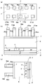
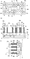
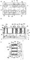
- 6A and 6B are a plan view and a cross-sectional structure diagram for explaining a method of manufacturing a columnar semiconductor device having an SGT according to the first embodiment.
- 6A and 6B are a plan view and a cross-sectional structure diagram for explaining a method of manufacturing a columnar semiconductor device having an SGT according to the first embodiment.
- 6A and 6B are a plan view and a cross-sectional structure diagram for explaining a method of manufacturing a columnar semiconductor device having an SGT according to the first embodiment.
- 6A and 6B are a plan view and a cross-sectional structure diagram for explaining a method of manufacturing a columnar semiconductor device having an SGT according to the first embodiment.
- 6A and 6B are a plan view and a cross-sectional structure diagram for explaining a method of manufacturing a columnar semiconductor device having an SGT according to the first embodiment.
- 6A and 6B are a plan view and a cross-sectional structure diagram for explaining a method of manufacturing a columnar semiconductor device having an SGT according to the first embodiment.
- 6A and 6B are a plan view and a cross-sectional structure diagram for explaining a method of manufacturing a columnar semiconductor device having an SGT according to the first embodiment.
- 6A and 6B are a plan view and a cross-sectional structure diagram for explaining a method of manufacturing a columnar semiconductor device having an SGT according to the first embodiment.
- 6A and 6B are a plan view and a cross-sectional structure diagram for explaining a method of manufacturing a columnar semiconductor device having an SGT according to the first embodiment.
- 6A and 6B are a plan view and a cross-sectional structure diagram for explaining a method of manufacturing a columnar semiconductor device having an SGT according to the first embodiment.
- 6A and 6B are a plan view and a cross-sectional structure diagram for explaining a method of manufacturing a columnar semiconductor device having an SGT according to the first embodiment.
- 6A and 6B are a plan view and a cross-sectional structure diagram for explaining a method of manufacturing a columnar semiconductor device having an SGT according to the first embodiment.
- 6A and 6B are a plan view and a cross-sectional structure diagram for explaining a method of manufacturing a columnar semiconductor device having an SGT according to the first embodiment.
- 6A and 6B are a plan view and a cross-sectional structure diagram for explaining a method of manufacturing a columnar semiconductor device having an SGT according to the first embodiment.
- 6A and 6B are a plan view and a cross-sectional structure diagram for explaining a method of manufacturing a columnar semiconductor device having an SGT according to the first embodiment.
- 6A and 6B are a plan view and a cross-sectional structure diagram for explaining a method of manufacturing a columnar semiconductor device having an SGT according to the first embodiment.
- 6A and 6B are a plan view and a cross-sectional structure diagram for explaining a method of manufacturing a columnar semiconductor device having an SGT according to the first embodiment.
- 6A and 6B are a plan view and a cross-sectional structure diagram for explaining a method of manufacturing a columnar semiconductor device having an SGT according to the first embodiment.
- 6A and 6B are a plan view and a cross-sectional structure diagram for explaining a method of manufacturing a columnar semiconductor device having an SGT according to the first embodiment.
- 6A and 6B are a plan view and a cross-sectional structure diagram for explaining a method of manufacturing a columnar semiconductor device having an SGT according to the first embodiment.
- 6A and 6B are a plan view and a cross-sectional structure diagram for explaining a method of manufacturing a columnar semiconductor device having an SGT according to the first embodiment.
- 6A and 6B are a plan view and a cross-sectional structure diagram for explaining a method of manufacturing a columnar semiconductor device having an SGT according to the first embodiment.
- 6A and 6B are a plan view and a cross-sectional structure diagram for explaining a method of manufacturing a columnar semiconductor device having an SGT according to the first embodiment.
- 6A and 6B are a plan view and a cross-sectional structure diagram for explaining a method of manufacturing a columnar semiconductor device having an SGT according to the first embodiment.
- 6A and 6B are a plan view and a cross-sectional structure diagram for explaining a method of manufacturing a columnar semiconductor device having an SGT according to the first embodiment.
- 6A and 6B are a plan view and a cross-sectional structure diagram for explaining a method of manufacturing a columnar semiconductor device having an SGT according to the first embodiment.
- 6A and 6B are a plan view and a cross-sectional structure diagram for explaining a method of manufacturing a columnar semiconductor device having an SGT according to the first embodiment.
- 6A and 6B are a plan view and a cross-sectional structure diagram for explaining a method of manufacturing a columnar semiconductor device having an SGT according to the first embodiment.
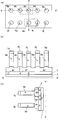
- 6A and 6B are a plan view and a cross-sectional structure diagram for explaining a method of manufacturing a columnar semiconductor device having an SGT according to the second embodiment of the present invention.
- 9A and 9B are a plan view and a cross-sectional structure diagram for explaining a method of manufacturing a columnar semiconductor device having an SGT according to the second embodiment.
- 9A and 9B are a plan view and a cross-sectional structure diagram for explaining a method of manufacturing a columnar semiconductor device having an SGT according to the second embodiment.
- 9A and 9B are a plan view and a cross-sectional structure diagram for explaining a method of manufacturing a columnar semiconductor device having an SGT according to the second embodiment.
- 9A and 9B are a plan view and a cross-sectional structure diagram for explaining a method of manufacturing a columnar semiconductor device having an SGT according to a third embodiment of the present invention.
- 9A and 9B are a plan view and a cross-sectional structure diagram for explaining a method of manufacturing a columnar semiconductor device having an SGT according to a third embodiment of the present invention.
- 9A and 9B are a plan view and a cross-sectional structure diagram for explaining a method of manufacturing a columnar semiconductor device having an SGT according to a third embodiment of the present invention.
- 9A and 9B are a plan view and a cross-sectional structure diagram for explaining a method of manufacturing a columnar semiconductor device having an SGT according to a third embodiment of the present invention.
- 9A and 9B are a plan view and a cross-sectional structure diagram for explaining a method of manufacturing a columnar semiconductor device having an SGT according to a third embodiment of the present invention.
- 9A and 9B are a plan view and a cross-sectional structure diagram for explaining a method of manufacturing a columnar semiconductor device having an SGT according to a third embodiment of the present invention.
- 9A and 9B are a plan view and a cross-sectional structure diagram for explaining a method of manufacturing a columnar semiconductor device having an SGT according to a fourth embodiment of the present invention.
- 9A and 9B are a plan view and a cross-sectional structure diagram for explaining a method of manufacturing a columnar semiconductor device having an SGT according to a fourth embodiment of the present invention.
- 9A and 9B are a plan view and a cross-sectional structure diagram for explaining a method of manufacturing a columnar semiconductor device having an SGT according to a fifth embodiment of the present invention.
- 9A and 9B are a plan view and a cross-sectional structure diagram for explaining a method of manufacturing a columnar semiconductor device having an SGT according to a fifth embodiment of the present invention.
- 9A and 9B are a plan view and a cross-sectional structure diagram for explaining a method of manufacturing a columnar semiconductor device having an SGT according to a fifth embodiment of the present invention.
- 9A and 9B are a plan view and a cross-sectional structure diagram for explaining a method of manufacturing a columnar semiconductor device having an SGT according to a fifth embodiment of the present invention.
- 9A and 9B are a plan view and a cross-sectional structure diagram for explaining a method of manufacturing a columnar semiconductor device having an SGT according to a fifth embodiment of the present invention.
- 9A and 9B are a plan view and a cross-sectional structure diagram for explaining a method of manufacturing a columnar semiconductor device having an SGT according to a fifth embodiment of the present invention.
- 9A and 9B are a plan view and a cross-sectional structure diagram for explaining a method of manufacturing a columnar semiconductor device having an SGT according to a sixth embodiment of the present invention.
- 9A and 9B are a plan view and a cross-sectional structure diagram for explaining a method of manufacturing a columnar semiconductor device having an SGT according to a seventh embodiment of the present invention.
- 9A and 9B are a plan view and a cross-sectional structure diagram for explaining a method of manufacturing a columnar semiconductor device having an SGT according to an eighth embodiment of the present invention.
- 9A and 9B are a plan view and a cross-sectional structure diagram for explaining a method of manufacturing a columnar semiconductor device having an SGT according to an eighth embodiment of the present invention.
- 9A and 9B are a plan view and a cross-sectional structure diagram for explaining a method of manufacturing a columnar semiconductor device having an SGT according to an eighth embodiment of the present invention.
- 9A and 9B are a plan view and a cross-sectional structure diagram for explaining a method of manufacturing a columnar semiconductor device having an SGT according to an eighth embodiment of the present invention.
- 9A and 9B are a plan view and a cross-sectional structure diagram for explaining a method of manufacturing a columnar semiconductor device having an SGT according to an eighth embodiment of the present invention.
- 9A and 9B are a plan view and a cross-sectional structure diagram for explaining a method of manufacturing a columnar semiconductor device having an SGT according to an eighth embodiment of the present invention.
- 9A and 9B are a plan view and a cross-sectional structure diagram for explaining a method of manufacturing a columnar semiconductor device having an SGT according to an eighth embodiment of the present invention.
- 9A and 9B are a plan view and a cross-sectional structure diagram for explaining a method of manufacturing a columnar semiconductor device having an SGT according to an eighth embodiment of the present invention. It is a schematic structure figure which shows SGT of a prior art example.
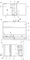
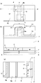
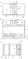
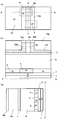
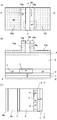
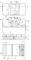
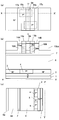
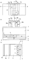
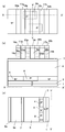
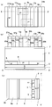
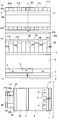
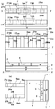
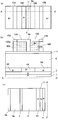
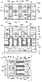
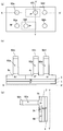
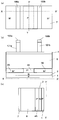
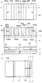
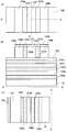
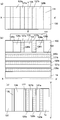
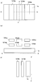
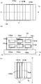
- FIGS. 1A to 1XX (A) is a plan view, (b) is a sectional structural view taken along line XX' of (a), and (c) is a sectional structural view taken along line YY' of (a).
- an N layer 2 is formed on a P layer substrate 1 by an epitaxial crystal growth method. Then, the N+ layer 3 and the P+ layers 4 and 5 are formed on the surface layer of the N layer 2 by the ion implantation method. Then, the i layer (intrinsic Si layer) 6 is formed. Then, a mask material layer 7 including, for example, a SiO 2 layer, an aluminum oxide (Al 2 O 3 , hereinafter referred to as AlO) layer, and a SiO 2 layer is formed. The i layer 6 may be formed of N-type or P-type Si containing a small amount of donor or acceptor impurities. Then, a silicon nitride (SiN) layer 8 is deposited. Then, a mask material layer 9 made of a SiO 2 layer is deposited. Then, the mask material layer 10 made of the SiN layer is deposited.
- SiN silicon nitride
- the mask material layer 10 is etched using a strip-shaped resist layer (not shown) extending in the Y direction in a plan view formed by the lithography method as a mask.
- the strip-shaped mask material layer 10a extending in the Y direction in plan view is formed.
- the band-shaped mask material layer 10a may be isotropically etched so that the width of the band-shaped mask material layer 10a is smaller than that of the resist layer.
- the strip mask material layer 10a having a width smaller than the minimum width of the resist layer that can be formed by the lithography method can be formed.
- the mask material layer 9 is etched by, for example, RIE (Reactive Ion Etching) to form the strip mask material layer 9a.
- RIE Reactive Ion Etching
- the cross section of the strip-shaped mask material layer 10a formed by isotropic etching has a trapezoidal shape with a bottom width larger than the top width, whereas the cross section of the mask material layer 9a is etched by RIE, and thus has a rectangular shape. Become. This rectangular cross section leads to improvement in the accuracy of the etching pattern using the strip mask 9a as a mask.
- the strip-shaped mask material layer 9a is used as a mask to etch the mask material layer 8 by, for example, the RIE method to form the strip-shaped mask material layer 8a.
- the aforementioned strip-shaped mask material layer 10a may be removed before etching the mask material layer 8 or may remain.
- the SiGe layer 12 and the SiO 2 layer 13 are entirely formed by the ALD (Atomic Layered Deposition) method into the mask material layer 7 (first material layer) and the strip mask material layer 8a.
- ALD atomic layered Deposition
- the cross section of the SiGe layer 12 (second material layer) has a roundness R1 at the top. It is desirable that the roundness R1 be formed so as to be located above the strip-shaped mask material layer 8a.
- the entire surface is covered with a SiO 2 layer (not shown) by, for example, a flow CVD (Flow Chemical Vapor Deposition) method, and the upper surface position is striped by CMP (Chemical Mechanical Polishing).
- the SiO 2 layer 13 (third material layer) and the SiGe layer 12 are polished so as to be located on the surface of the mask material layer 9a to form the SiO 2 layer 13a and the SiGe layers 12a and 12b.
- the rounded portion R1 at the top of the SiGe layer 12 in FIG. 1D be removed in the step of polishing the SiO 2 layer 13 and the SiGe layer 12.
- the tops of the SiGe layers 12a and 12b are etched to form recesses 14a and 14b (first recesses). It is desirable that the bottom positions of the recesses 14a and 14b be located below the mask material layer 9a, and that the top roundness R1 of the SiGe layers 12a and 12b be etched.
- the rounded portion R at the top of the SiGe layer 12 in FIG. 1D is removed, so that the concave portions 14a and 14b whose outer peripheral side surfaces are vertical are formed.
- SiN layers 15a and 15b (third strip material layers) having the same shape as the top shape of the SiGe layers 12a and 12b in plan view are formed on both sides of the strip mask material layers 8a and 9a.
- the band-shaped mask material layers 9a, 15a, 15b are used as masks to etch the SiGe layers 12a, 12b to form band-shaped SiGe layers 12aa, 12ab (fourth band-shaped material layer).
- the widths of the strip SiGe layer 12aa and the strip SiGe layer 12ab are the same in a plan view.
- the SiN layer 16 by the ALD method and the SiO 2 layer 13b by the FCVD method are formed so as to cover the entire surface.
- the SiO 2 layer 13b (fifth material layer), the SiN layer 16, and the upper surface of the mask material layer 9a are polished so that their upper surface positions are the same. Then, the same steps as those in FIGS. 1E and 1F are performed, and as shown in FIG. 1K, the strip-shaped SiN layers 16A and 16B are sandwiched between the strip-shaped mask material layers 15a and 15b and the SiO 2 layer 13ba.
- the recesses 14A and 14B (second recesses) are formed.
- the strip-shaped SiGe layers 12aa and 12ab are in contact with both side faces of the strip-shaped SiN layers 16a and 16b, and the strip-shaped mask material layers 15a and 15b are in contact with both side faces thereof. 5), and a strip-shaped material layer 5).
- a SiGe layer (not shown) is formed so as to cover the whole by ALD.
- a SiO 2 layer (not shown) is formed so as to cover the whole.
- polishing is performed so that the upper surface positions of the SiO 2 layer and the SiGe layer are the same as the upper surface position of the strip mask material layer 9a.
- the same steps as those in FIGS. 1E to 1I are performed, and as shown in FIG. 1M, the strip-shaped SiGe layers 18a and 18b contacting both side surfaces of the strip-shaped mask material layers 16a and 16b (sixth strip-shaped material layer) are formed.
- strip-shaped mask material layers 19a and 19b in contact with both side surfaces of the strip-shaped mask material layers 17a and 17b.
- a SiN layer (not shown) is formed so as to cover the whole by ALD.
- a SiO 2 layer (not shown) is formed so as to cover the whole.
- polishing is performed so that the upper surface positions of the SiO 2 layer and the SiN layer are the same as the upper surface position of the strip mask material layer 9a.
- the same steps as those in FIGS. 1E to 1I are performed, and as shown in FIG. 1N, the strip-shaped mask material layer layers 20a and 20b and the strip-shaped mask material layer which are in contact with both side surfaces of the strip-shaped mask material layer layers 20a and 20b.
- Strip-shaped mask material layers 21a and 21b in contact with both side surfaces of 19a and 19b are formed.
- the strip mask material layers 15a, 15b, 19a, 19b and the strip SiGe layers 12aa, 12ab, 18a, 18b are removed by etching.
- the strip-shaped mask material layers 8a, 16a, 16b, 20a, 20b and the mask material layers on the strip-shaped mask material layers 8a, 16a, 16b, 20a, 20b are formed on the mask material layer 7.
- 9a, 17a, 17b, 21a, 21b are formed.
- the entire surface is coated with a SiO 2 layer (not shown).
- the SiO 2 layer 22 is formed by CMP so that the upper surface position of the SiO 2 layer becomes the upper surface position of the strip-shaped mask material layer 9a.
- the SiN layer 24 and the SiGe layer are formed on the entire surface.
- the strip mask material layer 26 (eighth strip material layer) made of the SiN layer extended in the X direction is formed.
- the SiGe layer is etched by using the strip mask material layer 26 formed by the lithography method and the RIE method as a mask to form the strip SiGe layer 25 (the ninth strip material layer) extending in the X direction.
- strip-shaped mask material layer 26 and the strip-shaped SiGe layer 25 are removed, and the strip-shaped mask material layers 28a and 28b extended in the X direction on the SiN layer 24 in plan view. And strip-shaped mask material layers 27a and 27b on the strip-shaped mask material layers 28a and 28b are formed.
- the SiN layer 24 and the strip mask material layers 9a, 17a, 17b, 21a, 21b, 8a, 16a, 16b, 20a are masked with the strip mask material layers 27a, 27b, 28a, 28b.
- 20b and the SiO 2 layer 22 are etched.
- the strip-shaped SiN layer 24a is formed under the strip-shaped mask material layers 27a and 28a, the square-shaped mask material layers 21aa, 21ba, 17aa, 17ba, 9aa, and the square-shaped mask material layers 21aa, 21ba in plan view.
- Square-shaped mask material layers 20aa, 20ba, 16aa, 16ba, 8aa located under 17aa, 17ba, 9aa are formed.
- 17bb, 9ab, and square mask material layers 20ba (not shown), 20bb (not shown), 16ba (not shown), 16bb (not shown), and 8ab are formed. ..
- the SiO 2 layer 22a is formed under the band-shaped SiN layer 24a and between the band-shaped mask material layers 21aa, 21ba, 17aa, 17ba, 9aa, 20aa, 20ba, 16aa, 16ba, 8aa.
- a SiO 2 layer 22b (not shown) is formed below the strip-shaped SiN layer 24b and between the strip-shaped mask material layers 21ba, 21bb, 17ba, 17bb, 9ab, 20ba, 20bb, 16ba, 16bb, 8ab. To be done.
- the strip mask material layers 27a, 27b, 28a, 28b, the strip SiN layers 24a, 24b, and the SiO 2 layers 22a, 22b are removed.
- the square mask material layers 21aa, 21ab, 21ba, 21bb, 17aa, 17ba, 17ba, 17bb, 9aa, 9ba in a plan view and the square mask material layers 20aa, 20ab, 20ba, 20bb, 16aa, 16ab, 16ba, 16bb, 8aa, 8ab are formed.
- the mask material layers 21aa, 21ab, 21ba, 21bb, 17aa, 17ab, 17ba, 17bb, 9aa, 9ab and the mask material layers 20aa, 20ab, 20ba, 20bb, 16aa, 16ba, 16bb, 8aa, 8ab are removed.
- mask material layers 7a, 7b, 7c, 7d, 7e, 7f, 7g, 7h, 7i, 7j (first mask material layer) are formed on the i layer 6.
- One or both of 20ba, 20bb, 16aa, 16ab, 16ba, 16bb, 8aa, 8ab is lightly isotropically etched.
- the mask material layers 7a to 7j have a circular shape in plan view.
- the i layer 6 is etched to form Si pillars 6a, 6b, 6c, on the N+ layer 3 and the P+ layer 4.
- 6d, 6e, 6f, 6h, 6i and 6j three-dimensional semiconductor layer
- a SiO 2 layer (not shown) is coated by the FCVD method and then polished by the CMP method so that the surface positions are the top positions of the mask material layers 7a to 7j. Then, the mask material layers 7b and 7i and the Si pillars 6b and 6i are removed by the lithography method and the RIE etching method. Then, the SiO 2 layer formed by the FCVD method is removed. As a result, Si pillars 6a, 6c, 6d, 6e, 6f, 6h, 6j are formed on the N+ layer 3 and the P+ layers 4, 5 as shown in FIG. 1W.
- the mask material layers 7a to 7j are surrounded by the mask material layers 30a, 30b, 30c and 30d, and the Si pillars 6a to 6j (Si pillars).
- Mask material layers 31a, 31b, 31c and 31d (not shown) surrounding the side surfaces of the mask material 6b and 6i).
- the entire surface is covered with a SiO 2 layer (not shown) by the FCVD method, and then the surface position is made the top position of the mask material layers 7a to 7j (there is no mask material layers 7b and 7i) by the CMP method. To polish.
- the Si pillars 6a, 6c, 6d, and 6e are connected to each other, for example, the strip-shaped mask material layer 33a made of a SiO 2 layer and the Si pillars 6f, 6g, 6h, and 6j are connected.
- a band-shaped mask material layer 33b made of, for example, a SiO 2 layer is formed.
- the SiO 2 layer, N+ layer 3, P+ layers 4, 5, N layer 2, P layer 1 are formed by RIE. Etching.
- the N layer 2a, the N+ layers 3a, 3b, and the P+ layer 4a are formed under the Si pillars 6a, 6c, 6d, and 6e and on the P layer 1.
- the N layer 2b, the N+ layer 3c (not shown), 3d (not shown), and the P+ layer 5a which are under the Si pillars 6f, 6g, 6h, and 6j, and above the P layer 1, are formed. It is formed.
- the SiO 2 layer 32a is formed under the mask material layer 33a and between the Si pillars 6a and 6c.
- a SiO 2 layer 32b (not shown) is formed under the mask material layer 33b and between the Si pillars 6h and 6j.
- the mask material layers 33a, 33b, the SiO 2 layers 32a, 32b, and the mask material layers 30a, 30b, 30c, 30d, 31a, 31b, 31c, 31d are removed.
- an SiO 2 layer 34 is formed on the outer peripheral portions of the N+ layers 3a, 3b, 3c and 3d, the P+ layers 4a and 5a, the N layers 2a and 2b, and the P layer substrate 1. Then, an HfO 2 layer (not shown), a TiN layer (not shown), and a SiO 2 layer (not shown) are formed to cover the whole by ALD. In this case, it is desirable that the TiN layers between the Si pillars 6c, 6d and 6e are in contact with each other at their side surfaces. Similarly, it is desirable that the TiN layers between the Si pillars 6f, 6g, and 6h are in contact with each other at their side surfaces.
- the SiO2 layer is etched back by the RIE method.
- the TiN layer and the HfO2 layer are etched so that the upper surface positions are the upper positions of the Si pillars 6a to 6j.
- a SiN layer (not shown) is formed to cover the entire surface by the CVD method.
- the SiN layer is polished by the CMP method so that the upper surface positions are the upper surface positions of the mask material layers 7a to 7j.
- SiN layers 37a, 37b, 37c, 37d (not shown) of equal width in plan view are formed on the outer circumferences of the tops of the Si pillars 6a to 6j.
- the mask material layers 38a, 38b, 38c, 38d that are in contact with the Si pillars 6a, 6d, 6g, 6j in plan view are formed on the upper surfaces of the mask material layers 7a to 7j.
- the mask material layers 7a to 7j, 37a, 37b, 37c, 37d, 38a, 38b, 38c, 38d are used as masks, SiO 2 on the outer peripheral portions of the mask material layers 37a, 37b, 37c, 37d in plan view.
- a TiN layer 40d (not shown) connected to the outer peripheral portion of the Si pillar 6j is formed. Then, the mask material layers 38a to 38d, 37a to 37d, 7a to 7j are removed.
- the entire surface is covered with a SiO 2 layer (not shown), and then the upper surface position of the SiO 2 layer becomes the upper surface positions of the tops of the Si pillars 6a to 6j by the CMP method.
- the upper part of the SiO 2 layer is etched by the RIE method so that the upper surface positions thereof reach the top positions of the TiN layers 40a to 40d.
- the SiN layer 42 is formed on the outer peripheral portions of the tops of the Si pillars 6a to 6j.
- an N+ layer 43a containing a donor impurity is formed by a selective epitaxial crystal growth method so as to surround the tops of the Si pillars 6a.
- a SiO 2 layer (not shown) is formed to cover the Si pillars 6a, 6d, 6e, 6f, 6g, 6j.
- P+ layers 43b and 43g containing acceptor impurities are formed by the selective epitaxial crystal growth method so as to surround the tops of the Si pillars 6c and 6h.
- the donor impurities of the N+ layers 43a, 43c, 43d, 43e, 43f, 43h are diffused to the tops of the Si pillars 6a, 6d, 6e, 6f, 76g, 6j, and the N+ layers 44a, 44c, 44d, 44e (not shown), 44f (not shown), and 44h (not shown) are formed.
- acceptor impurities are diffused from the P+ layers 43b and 43g to form P+ layers 44b and 44g.
- a SiO 2 layer 46 having a flat upper surface is formed so as to cover the entire surface.
- the connection wiring metal layer C1 is formed through the contact hole 47a formed on the boundary surface between the N+ layer 3a and the P+ layer 4a and on the TiN layer 40b.
- the connection wiring metal layer C2 (not shown) is formed on the boundary surface between the N+ layer 3d and the P+ layer 5a, the TiN layer 40b, and the contact hole 47b formed on the TiN layer 40b.
- a SiO 2 layer 48 having a flat upper surface is formed so as to cover the entire surface.
- the word metal wiring layer WL is formed through the contact holes 49a and 49bc formed on the TiN layers 40a and 40d.
- a SiO 2 layer 50 having a flat upper surface is formed so as to cover the entire surface.
- the ground wiring layer Vss1 is formed through the contact holes 51a and 51b formed on the N+ layers 43c and 43d.
- the ground wiring layer Vss2 is formed through the contact holes 51c and 51d formed on the N+ layers 43e and 43f.
- a SiO 2 layer 52 having a flat upper surface is formed so as to cover the entire surface.
- the power supply metal wiring layer Vdd is formed through the contact holes 53a and 53b formed on the P+ layers 43b and 43g.
- bit output metal wiring layer BL and the inverted bit output wiring layer RBL are formed through the contact holes 55a and 55b formed on the N+ layers 43a and 43h. As a result, the SRAM cell circuit is formed on the P layer substrate 1.
- ten Si pillars 6a to 6j are formed in one SRAM cell region.
- the lithography method was used only for forming the strip-shaped SiN layer 8a for forming one column of Si pillars (6c, 6h) in the X direction.
- the other eight Si pillars (6a to 6j except 6c and 6h) are formed by the band-shaped SiGe layers 12aa, 12ab, 18a, 18b and the band-shaped SiN layers 16a, 16b, 20a, 20b formed by the ALD method. ..
- the band-shaped SiGe layers 12a and 12b were formed by the ALD method, and the band-shaped mask material layers 15a and 15b having a shape in which the top shape of the band-shaped SiGe layers 12a and 12b remained as they were were formed on the band-shaped SiGe layers 12a and 12b. ..
- the ALD method one atomic layer or one molecular layer can be deposited with good controllability. Thereby, in plan view, the thickness of the strip-shaped SiGe layers 12a and 12b can be made highly precise and narrow according to the requirements from the design. As a result, the distance between the Si pillars 7a to 7j can be made highly precise and narrow without restrictions of lithography. As a result, the SRAM cell can be highly integrated.
- the strip-shaped SiGe layers 12aa, 12ab Only the strip-shaped mask material layers 15a and 15b may be formed by the manufacturing method provided by the present invention. 2.
- the diameter of the Si pillars 7a to 7j in plan view can be made highly precise and small without restrictions of lithography.
- the cell design can be performed without the limitation on the high integration of the cell by lithography.
- the SRAM cell can be highly accurate and highly integrated. 3.
- it is required to improve the precision and the density of both the diameter of the Si pillars 6a to 6j in plan view and the distance between the Si pillars 6a to 6j.
- the present embodiment in the present embodiment, for example, as shown in FIGS.
- the strip-shaped SiGe layers 12aa and 12ab formed on both side surfaces of the strip-shaped SiN layer 8a in the X-direction cross section. , 18a, 18b and the strip-shaped SiN layers 16a, 16b, 20a, 20b can be formed with high precision and narrowly. Increasing the accuracy of the thickness of the strip-shaped SiN layers 16a, 16b, 20a, 20b leads to increasing the accuracy of the diameter of the Si pillars 6a to 6j. The higher accuracy of the thickness of the band-shaped SiGe layers 12aa, 12ab, 18a, 18b leads to the higher accuracy of the distance between the Si pillars 6a to 6j.
- the strip-shaped mask material layers 15a, 15b, 17a, 17b are etched by the RIE method of the SiGe layers 12a, 12b and the SiN layers 16A, 16B, although the portions exposed to etching ions have a low etching rate. If the strip mask material layers 15a, 15b, 17a, 17b are, for example, trapezoidal with the lower side longer than the upper side, the bottom portions of the strip mask material layers 15a, 15b, 17a, 17b are etched during etching. As a result, the positions of the mask layer ends of the strip-shaped mask material layers 15a, 15b, 17a, 17b in plan view change with the etching time.
- the SiGe layers 12a and 12b and the SiN layers 16A and 16B having the same thickness in the vertical direction are formed on both sides of the strip SiN layer 8a and the strip mask material layer 9a.
- band-shaped mask material layers 15a, 15b, 17a, 17b were formed by leaving the top shapes of the SiGe layers 12a, 12b and SiN layers 16A, 16B as they were.
- band-shaped mask material layers 15a, 15b, 17a, 17b having a rectangular cross section are formed.
- the SiGe layers 12a, 12b and the SiN layers 16A, 16B are etched using the strip-shaped mask material layers 15a, 15b, 17a, 17b having a rectangular cross section as masks, whereby the strip-shaped SiGe layers 12aa, 12ab having a rectangular cross section. , Band-shaped SiN layers 16a and 16b are formed.
- the SRAM cell can be made highly accurate and highly integrated. 5. For example, as shown in FIGS.
- the strip-shaped SiN layer 8a and the strip-shaped mask material layer 9a are covered, and SiGe is formed by the ALD method.
- Layer 12 was deposited.
- a SiO 2 layer (not shown) was deposited.
- the SiO 2 layer and the SiGe layer 12 were polished by the CMP method so that the upper surface positions of the SiO 2 layer and the SiGe layer 12 were the upper surface positions of the strip mask material layer 9a. By this polishing, the upper roundness R1 of the SiGe layer 12 was removed.
- the shapes of the depressions 14a and 14b are the same as the strip-shaped mask material layers 9a on both side surfaces of the SiGe layers 12a and 12b and the side surface shape of the SiO 2 layer 13 and have a uniform width in the vertical direction. It is formed along the shape of the SiGe layers 12a and 12b. Therefore, the cross-sectional shape of the recesses 14a and 14b is formed into a substantially rectangular shape. As a result, the cross-sectional shape of the strip-shaped mask material layers 15a and 15b is maintained to have a uniform width in the vertical direction, and the overall shape is substantially rectangular.
- the band-shaped SiGe layers 12aa and 12ab formed by forming the SiGe layer 12a by using the band-shaped mask material layers 15a and 15b as masks by the RIE method can be formed with high accuracy in both plan view and cross-sectional view.
- the band-shaped SiN layers 16a, 16b, 20a, 20b and the band-shaped SiGe layers 18a, 18b can be formed with high precision. 6.
- the Si pillars 7c, 7d, 7e and the gate TiN layers 40b, 40c connected to the outer periphery of the Si pillars 7f, 7g, 7h are arranged between the Si pillars 7c, 7d, 7e.
- Si pillars 7f, 7g, and 7h are in contact with each other on their side surfaces.
- the gate TiN layers 40a and 40d are formed independently.
- the Si pillars 7c, 7d, 7e and the gate TiN layers 40b, 40c connected to the outer circumferences of the Si pillars 7f, 7g, 7h are between the Si pillars 7c, 7d, 7e and between the Si pillars 7f, 7g, 7h.
- the contact between the side surfaces means that the distance between the Si pillars 7c, 7d and 7e and the distance between the Si pillars 7f, 7g and 7h is added to the gate HfO layer 35 and the gate TiN layers 40b and 40c. It shows that it can be shortened to twice the thickness. Then, as shown in FIG. 1W, by removing the Si pillars 7b and 7i, the gate TiNs 40a and 40c can be formed apart from the gate TiN layers 40b and 40d. This is because, as shown in FIG. 1W, after the Si pillars 6a to 6j are formed in high density in a plan view, the Si pillars 7b and 7i are removed to form a region without the Si pillars in a plan view.
- the contact holes 47a and 47b can be formed on the removed regions of the Si pillars 7b and 7i in a plan view. As a result, the density of the SRAM cell can be increased.
- the present embodiment is applicable not only to SRAM cells, but also to circuits having a plurality of Si pillars in which gate conductor layers are connected to each other and one or a plurality of Si pillars adjacent to and separated from each other. Can be applied. 7. In the present embodiment, as described in FIGS.
- the strip mask material layer 27a extending in the X direction is orthogonal to the strip mask material layers 8a, 16a, 16b, 20a, 20b extending in the Y direction, 27b, 28a and 28b were formed by the same method as that for forming the strip mask material layers 8a, 16a, 16b, 20a and 20b.
- the Si pillars 6a to 6j are formed with high accuracy and high density in both the X and Y directions.
- the strip mask material layers 8a, 16a, 16b, 20a, 20b are formed first, and then the strip mask material layers 28a, 28b are formed.
- the Si pillars 6a to 6j are also highly accurately and densely formed. Can be formed.
- this method is not used, and after the mask material layer is formed on the entire surface, the strip-shaped mask material layers 27a, 27b, 28a are directly formed by the lithography method and the RIE etching method. , 28b may be formed.
- the mask material layer is formed over the entire surface without using this method, and then the mask material layers 8a, 16a, 16b, 20a, 16a, 16b, 20a are directly formed by the lithography method and the RIE etching method. 20b or the strip-shaped mask material layers 9a, 17a, 17b, 21a, 21b may be formed. 8.
- the present embodiment as shown in FIG. 1O, five strip-shaped SiN layers 8a, 16a, 16b, 20a, 20b extending in the Y direction are formed in a plan view.
- Si pillars can be formed with high density at the position of the band-shaped SiN layer on the plane.
- FIGS. 2A to 2D (Second embodiment) Hereinafter, a method of manufacturing a columnar semiconductor device having an SGT according to the second embodiment of the present invention will be described with reference to FIGS. 2A to 2D.
- (A) is a plan view
- (b) is a sectional structure view taken along line XX' of (a)
- (c) is a sectional structure view taken along line YY' of (a).
- the N+ layer 3 and the P+ layer 4 in FIG. 1A have different arrangements in a plan view, and strip N+ layers 3A and 3B are formed on both sides of the strip P+ layer 4A as shown in FIG. 2A.
- SiGe layers 12Aa and 12Ab having a width wider than that of the band-shaped SiGe layers 12aa and 12ab in plan view are formed on both sides of the band-shaped SiN layer 8a having the band-shaped mask material layer 9a on the top.
- Band-shaped mask material layers 15A and 15B are formed on the tops of the SiGe layers 12Aa and 12Ab.
- the strip-shaped SiN layers 16A and 16B having the strip-shaped mask material layers 17A and 17B on the tops and having the same width as the strip-shaped SiN layer 8a are formed on both sides of the strip-shaped SiGe layers 12Aa and 12Ab.
- FIG. 2B a square SiN layer having the mask material layers 9Aa, 9Ab, 17Aa, 17Ab, 17Ba, 17Bb, which are square in plan view, on the mask material layer 7 as shown in FIG. 2B. 8Aa, 8Ab, 16Aa, 16Ab (not shown), 16Ba, 16Bb (not shown) are formed.
- Si pillars 61a, 61c, 61d, 61f are formed on the N+ layers 3A, 3B.
- Si pillars 61b and 61e are formed on the P+ layer 4A.
- the same steps as those in FIGS. 1X to 1YY are performed.
- the N layer 2A, the N+ layers 3Aa, 3Ba, and the P+ layer 4Aa are formed under the Si pillars 61a, 61b, 61c.
- the N layer 2B, the N+ layer 3Ba (not shown), 3Bb (not shown), and the P+ layer 4Ba are formed under the Si pillars 61d, 61e, and 61f.
- the SiO 2 layer 33 is formed so as to surround the lower portions of the Si pillars 61a to 61f.
- the HfO 2 layer 63 that is a gate insulating layer is formed so as to surround the Si pillars 61a to 61f.
- the gate TiN layers 65a, 65b, 65c, 65d (not shown) and the SiO 2 layer 41 are formed so as to surround the HfO 2 layer 63.
- the SiO 2 layer 42 is formed on the outer periphery of the tops of the Si pillars 61a to 61f.
- N+ layers 67a, 67c, 67d, 67f and P+ layers 67b, 67e are formed on the tops of the Si pillars 61a to 61f by the selective epitaxial crystal growth method.
- N+ layers 66a, 66c, 67d (not shown) and 67f (not shown) and P+ layers 66b and 66e on top of the Si pillars 61a to 61f.
- a metal layer (not shown) is formed through the contact hole 69a formed on the boundary between the N+ layer 3Aa, the P+ layer 4Aa, and the gate TiN layer 65c. ), the N+ layer 3Aa and P+ layer 4Aa are connected to the gate TiN layer 65c.
- the metal layer (not shown) formed on the boundary between the N+ layer 3Bb and the P+ layer 4Ba and the contact hole 69b formed on the gate TiN layer 65b allows the N+ layer 3Bb, the P+ layer 4Ba and the gate TiN layer to be formed. Make a connection to layer 65b. Then, after forming the SiO 2 layer 48 on the entire surface, the gate TiN layers 65a and 65d are formed via the contact hole 70a formed on the gate TiN layer 65a and the contact hole 70b formed on the gate TiN layer 65d. , And the word line metal layer WL are connected.
- the P+ layers 67b and 67e and the power supply wiring metal layer Vdd are connected via the contact holes 71a and 71b formed on the P+ layers 67b and 67e.
- the SiO 2 layer 52 is formed over the entire surface, the N+ layer 67a and the ground wiring metal layer Vss1 are connected via the contact hole 73a.
- the N+ layer 67f and the ground wiring metal layer Vss2 are connected via the contact hole 73b.
- the SiO 2 layer 54 is formed over the entire surface, the N+ layer 67c and the bit wiring metal layer BL are connected via the contact hole 74a.
- the N+ layer 67d and the inverted bit wiring metal layer RBL are connected via the contact hole 74b.
- the SRAM cell is formed on the P layer substrate 1.
- the manufacturing method of this embodiment the following features are obtained. 1.
- five strip-shaped SiN layers 8a, 16a, 16b, 20a, 20b were formed on the mask material layer 7.
- FIG. 2A three strip-shaped SiN layers 8a, 16A, 16B can be formed to form an SRAM cell. Thereby, the process can be simplified.
- a step of removing the Si pillars 6b and 6i formed in the SRAM cell region was required.
- the present invention does not require such a Si pillar removing step. Thereby, the process can be simplified.
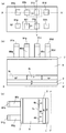
- FIGS. 3A to 3F are plan views
- (b) is a sectional structure view taken along line XX' of (a)
- (c) is a sectional structure view taken along line YY' of (a).
- the strip-shaped SiGe layer 80 having the strip-shaped mask material layer 81 on the apex has equal widths, and the strip-shaped mask material layers 83a and 83b (the third strip-shaped material layer) on the apex. ), the strip-shaped SiN layers 82a and 82b (fourth strip-shaped material layer) are formed.
- strip-shaped SiGe layers 84a and 84b having the strip-shaped mask material layers 85a and 85b on the tops are formed on both sides of the strip-shaped SiN layers 82a and 82b with equal widths.
- band-shaped SiN layers 86a and 86b having band-shaped mask material layers 87a and 87b on the tops thereof are formed on both sides of the band-shaped SiGe layers 84a and 84b.
- the same steps as shown in FIGS. 1D to 1M are performed.
- the square mask material layers 91a, 91b, 91c, 91d, 91e, 91f, 91g, and 91h are formed on the top portion of the mask material layer 7 in plan view.
- Layer-shaped square SiN layers 90a, 90b, 90c, 90d, 90e (not shown), 90f (not shown), 90g, 90h (not shown) are formed.
- the Si pillar 93a having the mask material layers 92a, 92b, 92c, 92d, 92e, 92f, 92g, and 92h on the N+ layer 3c, P+ layers 4c, and 4d is formed.
- 93b, 93c, 93d, 93e, 93f, 93g, 93h three-dimensional semiconductor layer are formed.
- the mask material layers 92b and 92g and the Si pillars 93b and 93g are removed.
- the N layer 2ca, the N+ layers 3ca, 3cb, and the P+ layer 4ca are formed under the Si pillars 93a, 93c, and 93d.
- the N layer 2cb, the N+ layer 3da (not shown), 3db (not shown), and the P+ layer 4cb are formed under the Si pillars 93e, 93f, and 93h.
- the HfO 2 layer 95 which is a gate insulating layer is formed so as to surround the Si pillars 93a to 93h.
- the gate TiN layers 96a, 96b, 96c, 96d (not shown) are formed so as to surround the HfO2 layer 95.
- N+ layers 98a, 98c, 98d (not shown), 98f (not shown) are provided on top of the Si pillars 93a, 93d, 93e, 93h, and N+ are provided on top of the Si pillars 93a, 93d, 93e, 93h.
- Layers 97a, 97c, 97d (not shown), 97e (not shown) are formed.
- P+ layers 98b and 98e are formed on the tops of the Si pillars 93c and 93f, and P+ layers 97b and 97e are formed on the tops.
- the N+ layer 3ca, the P+ layer 4ca and the gate TiN are formed by the metal layer (not shown) formed on the boundary between the N+ layer 3ca and the P+ layer 4ca and the contact hole 100a formed on the gate TiN layer 96c. A connection with the layer 95c is made.
- the metal layer (not shown) formed on the boundary between the N+ layer 3db and the P+ layer 4cb and the contact hole 100b formed on the gate TiN layer 96b allows the N+ layer 3db, the P+ layer 4cb and the gate TiN layer to be formed.
- a connection is made with layer 96b.
- the gate TiN layers 96a and 96d are connected to the word wiring metal layer WL via the contact hole 101a formed on the gate TiN layer 96a and the contact hole 100b formed on the gate TiN layer 96d.
- the P+ layers 98b and 98e are connected to the power supply wiring metal layer Vdd through the contact holes 102a and 102b formed on the P+ layers 98b and 98e.
- the N+ layer 98c and the ground wiring metal layer Vss1 are connected via the contact hole 103a.
- the N+ layer 98d and the ground wiring metal layer Vss2 are connected via the contact hole 103b.
- the N+ layer 98a and the inverted bit wiring metal layer RBL are connected via the contact hole 104a.
- the N+ layer 98f and the bit wiring metal layer BL are connected via the contact hole 104b.
- the SRAM cell is formed on the P layer substrate 1.
- the Si pillars 93c and 93d and the gate TiN layers 96b and 96c connected to the outer circumferences of the Si pillars 93e and 93f are provided between the Si pillars 93c and 93d and between the Si pillars 93e and 93e.
- the sides of 93f are in contact with each other.
- the gate TiN layers 96a and 96d are independently formed.
- the fact that the gate TiN layers 96b and 96c are in contact with each other on the side surfaces of the Si pillars 93c and 93d and between the Si pillars 93e and 93f means that the Si pillars 93c and 93d are connected to each other and the Si pillars 93e and 93f are connected to each other. It is shown that the distance between 93f can be shortened to twice the thickness of the gate HfO layer 95 and the gate TiN layers 96b and 96c. As a result, the SRAM cell can be highly integrated.
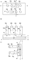
- FIGS. 4A and 4B are plan views
- (b) is a sectional structure view taken along line XX' of (a)
- (c) is a sectional structure view taken along line YY' of (a).
- the strip-shaped mask material layers 27a and 28a in the region on the SiN layer 16a in FIG. 1P are removed in a plan view by the lithography method and the RIE etching, and the strip-shaped mask material layer 27A is formed on the top.
- 27B having strip-shaped mask material layers 28A and 28B are formed.
- the strip mask material layers 27b and 28b on the SiN layer 16b are removed to form strip mask material layers 28C and 28D (not shown) having strip mask material layers 27C and 27D on their tops.
- the mask material layers 21aa, 21ba, 21ab, 21bb, 17ba having a square shape in plan view are formed on the mask material layer 7.
- 17ab, 9aa, 9ab and square mask material layers 20aa, 20ab, 20ba (not shown), 20bb, 16ab (not shown), 8aa, 8ab are formed.
- the SiN layers 16aa and 16bb and the mask material layers 17aa and 17bb in FIG. 1S are not provided.
- the SRAM cell having the same structure as that of the first embodiment is formed on the P layer substrate 1 by performing the steps of FIGS. 1X to 1YY.
- the Si pillars 6b and 6i and the mask material layers 7b and 7i are removed.
- the Si pillars 6b, 6i having a height in the vertical direction are etched with good control so that the etching end point becomes the same as the bottom of the other Si pillars 6a, 6c, 6d, 6e, 6f, 6h, 6j.
- the mask material layers 27a, 27b, 28a, 28b on the uppermost surface shown in FIG. 1P in the first embodiment may be etched.
- the etching end point is the mask material layer 7 which is an etching stopper, and there is no problem of controllability regarding the etching end point as in the first embodiment.
- FIGS. 5A to 5F are plan views
- (b) is a sectional structure view taken along line XX' of (a)
- (c) is a sectional structure view taken along line YY' of (a).
- a strip-shaped SiN layer 101a having a strip-shaped mask material layer 100a and a strip-shaped mask material layer 100b (sixth strip material layer, eleventh strip material layer, fifteenth strip material layer) on the top,
- the strip SiN layer 101b (seventh strip material layer, twelfth strip material layer, sixteenth strip material layer) is extended in the Y direction and formed on the mask material layer 7.
- the strip SiN layer 101a is formed on the N+ layer 3A in a plan view.
- the strip SiN layer 101b is formed on the N+ layer 3B in a plan view.
- the N+ layers 3A and 3B are formed in a strip shape on both sides of the strip P+ layer 4A in a plan view.
- strip mask material layers 102aa and 102ab and strip SiGe layers 103aa and 103ab are formed on both sides of the strip mask material layer 100a and the strip SiN layer 101a.
- the strip-shaped mask material layers 100b and 102bb (eighth strip-shaped material layer, 13th strip-shaped material layer, 17th strip-shaped material layer) and strip-shaped SiGe are formed on both sides of the strip-shaped mask material layer 100b and the strip-shaped SiN layer 101b.
- Layers 103ba and 103bb (a ninth strip material layer, a fourteenth strip material layer, and an eighteenth strip material layer) are formed.
- the entire SiN layer (not shown) is covered.
- the strip-shaped SiN layers 104a (19th strip-shaped material layers), 104b, and 104b are polished by CMP so that the upper surface positions of the SiN layers are the same as those of the mask material layers 100a, 100b. 104c is formed.
- a resist layer 105 having an opening end is formed outside the SiN layer 104C in plan view. Then, by using the resist layer 105 and the strip-shaped mask material layers 102ab and 102ba as a mask, etching is performed so that the upper surface position of the SiN layer 104a becomes the bottom position of the strip-shaped mask material layers 102ab and 102ba to form the recess 106. ..
- the resist layer 105 is removed.
- the concave portion 106 is filled by using the CVD method and the CMP method, and the strip-shaped mask material layer 108 (the twentieth strip-shaped material layer) whose upper surface position is the same as the upper surface positions of the strip-shaped mask material layers 102ab and 102ba is formed.
- the SiN layer 104 is removed by etching using the mask material layers 100a, 100b, 102aa, 102ab, 102ba, 102bb as masks.
- the strip mask material layers 102aa, 102ab, 102ba, and 102bb are removed.
- the SiGe layers 103aa, 103ab, 103ba, 103bb are removed.
- the strip-shaped SiN layers 101a, 101b, 104a having the mask material layers 100a, 100b, 108 on their tops are formed on the mask material layer 7.
- the SRAM cell circuit including the six Si pillars 61a to 61f is formed in one cell region, which is the same as the second embodiment.
- the following features are obtained.
- the two band-shaped SiN layers 16A and 16B are formed outside the band-shaped SiN layer 8a.
- the positional accuracy of the strip-shaped SiN layers 16A and 16B in the X direction with respect to the strip-shaped SiN layer 8a is determined by two ALD film depositions for forming the strip-shaped SiGe layers 12Aa and 12Ab and the strip-shaped SiN layers 16A and 16B. Then, the RIE etching accuracy affects.
- the strip-shaped SiN layers 101a and 101b on both sides are first formed, then the strip-shaped SiGe layers 103aa, 103ab, 03ba and 103bb are formed, and then the central strip-shaped SiN layer 104a is formed. ..
- the positional accuracy of the strip-shaped SiN layers 101a and 101b with respect to the strip-shaped SiN layer 104a in the X direction is determined by one ALD film deposition and RIE etching for forming the strip-shaped SiGe layers 103aa, 103ab, 03ba, and 103bb. Only accuracy affects. This makes it possible to improve the accuracy of the SRAM cell.
- the strip mask material layers 102aa, 102ab, 102ba, 102bb and the strip SiGe layers 103aa, 103ab, 10ba, 103bb are removed, and the strip mask material layers 100a, 100b, 108, SiN layers 101a, 101b, 104a was left.
- the strip mask material layers 102aa, 102ab, 102ba, 102bb and the strip SiGe layers 103aa, 103ab, 10ba, 103bb are left, and the strip mask material layers 100a, 100b, 108, SiN layers 101a, 101b, 104a are removed. You may let me.
- the strip-shaped mask material layers 102aa, 102ab, 102ba, 102bb and the strip-shaped SiGe layers 103aa, 103ab, 10ba, 103bb serve as mask material layers for forming Si pillars. This also makes it possible to improve the accuracy of the SRAM cell.
- This embodiment has been described with reference to an example in which the strip SiN layer 104a and the strip mask material layer 108 are formed between the strip SiGe layers 103ab and 103ba as shown in FIGS. 5B to 5E.
- the band-shaped mask material layer (not shown) and the band-shaped SiN layer (not shown) are formed as in the steps shown in FIGS. 1J to 1L. 5B, it is possible to form five strip-shaped mask material layers (not shown) extending in the same Y direction as in FIG. 1N and a strip-shaped SiN layer (not shown) in plan view.
- an SRAM cell including eight SGTs which is the same as in the first embodiment, can be formed.
- the number of steps for forming the strip mask material layer and the strip SiN layer can be reduced once from the first embodiment. This simplifies the process.
- FIG. (A) is a plan view
- (b) is a sectional structure view taken along line XX' of (a)
- (c) is a sectional structure view taken along line YY' of (a).
- Si layers 110a and 110b are formed instead of the SiGe layers 12a and 12b.
- an amorphous SiOC layer 111 is formed.
- heat treatment is performed in an atmosphere containing oxygen to oxidize the tops of the Si layers 110a and 110b to form band-shaped SiO 2 layers 112a and 112b which are mask material layers.
- the strip-shaped mask material layer can be formed by the oxidation treatment.
- the manufacturing method of this embodiment the following features are obtained.
- a step of polishing the entire deposited SiN layer by the CMP method was necessary.
- the strip-shaped SiO 2 layers 112a and 112b which are the mask material layers, can be formed only by the oxidation treatment. Thereby, the process can be simplified.
- FIG. 7 (A) is a plan view, (b) is a sectional structure view taken along line XX' of (a), and (c) is a sectional structure view taken along line YY' of (a).
- band-shaped nitrided SiGe layers 114a and 114b are formed on the top of the SiGe layer 12a by nitrogen ion implantation.
- the band-shaped nitrided SiGe layers 114a and 114b are used as mask material layers.
- the manufacturing method of this embodiment the following features are obtained.
- a step of polishing the entire deposited SiN layer by the CMP method was necessary.
- the band-shaped nitride SiGe layers 114a and 114b which are the mask material layers, can be formed only by ion implantation of nitrogen ions. Thereby, the process can be simplified.
- FIGS. 8A to 8E (Eighth Embodiment) Hereinafter, a method for manufacturing a three-dimensional semiconductor device according to the eighth embodiment of the present invention will be described with reference to FIGS. 8A to 8E.
- (A) is a plan view
- (b) is a sectional structure view taken along line XX' of (a)
- (c) is a sectional structure view taken along line YY' of (a).
- a SiGe layer 120a (fourth material layer) is formed by, for example, the ALD method on the SiO 2 substrate 1a. Then, the Si layer 121a (first semiconductor layer), the SiGe layer 120b (fourth material layer), the Si layer 121b (first semiconductor layer), and the SiGe layer 120c are sequentially formed from the bottom by the epitaxial crystal growth method. To do. A holding material layer (not shown) is formed on both ends of the SiGe layers 120a (eighth material layer), 120b (eighth material layer), 120c, and the Si layers 121a, 121b, 120c in the Y direction. .. Then, the mask material layer 122 is formed on the SiGe layer 120c.
- the same steps as those of FIGS. 1A to 1L are performed to form the strip-shaped SiN layer 124 having the strip-shaped mask material layer 125 on the top and the strip-shaped mask material layer 125 and the strip-shaped SiN layer 124 on both sides of the mask material layer 122.
- the strip-shaped SiGe layers 126a and 126b having the strip-shaped mask material layers 127a and 127b on the tops, and the mask material layers 129a and 129b on the tops on both sides of the strip-shaped SiGe layers 126a and 126b and the strip-shaped mask material layers 127a and 127b.
- the strip SiN layers 128a and 128b are formed.
- the entire surface is covered with a SiO 2 layer (not shown), and the SiO 2 layer 130 is polished by the CMP method so that the upper surface position becomes the upper surface position of the strip mask material layer 125. To form. Then, the mask material layer 131 whose both ends in the Y direction in plan view coincide with the end portions of the holding material layer is formed.
- the SiO2 layer 130, the strip mask material layers 125, 127a, 127b, 129a, 129b, the SiN layers 124, 128a, 128b, and the strip SiGe layers 126a, 126b are etched. Then, the mask material layer 131 is removed. Then, the remaining SiO layer 130, mask material layers 127a and 127b, and SiGe layers 126a and 128b are removed. Then, as shown in FIG.
- the mask material layer 125, the SiGe layers 120a, 120b, 120c, and the Si layers 121a, 121b are etched using the mask material layers 125, 129a, 129b and the SiN layers 124, 128a, 128b as masks. Then, under the SiN layer 128a, SiGe layers 120aa, 120ba, 120ca, Si layers 121aa, 121ba, and a mask material layer 122a are formed. At the same time, under the SiN layer 124, SiGe layers 120ab, 120bb, 120ba, Si layers 121ab, 121bb, and a mask material layer 122b are formed. At the same time, the SiGe layers 120ac, 120bc, 120cc, the Si layers 121ac, 121bc, and the mask material layer 122c are formed under the SiN layer 128b.
- the mask material layers 125, 129a, 129b, SiN layers 124, 128a, 128b, and SiGe layers 120aa, 120ab, 120ac, 120ba, 120bb, 129bc, 120ca, 120cb, 120cc are etched.
- band-shaped Si layers 121aa, 121ab, 121ac, 121ba, 121bb, 121bc supported by the holding material layers at both ends in the Y direction are formed.
- gate HfO layers 130aa, 130ab, 130ac, 130ba, 130bb, and 130bc are formed surrounding the strip-shaped Si layers 121aa, 121ab, 121ac, 121ba, 121bb, and 121bc.
- the gate YiN layer 131 is formed so as to surround the gate HfO layers 130aa, 130ab, 130ac, 130ba, 130bb, and 130bc.
- the holding material layers on both ends of the strip-shaped Si layers 121aa, 121ab, 121ac, 121ba, 121bb, 121bc are removed.
- an N+ layer (not shown) or a P+ layer (not shown) serving as a source or a drain is formed on both ends of the strip-shaped Si layers 121aa, 121ab, 121ac, 121ba, 121bb, 121bc.
- a circuit using a GAA (Gate All Around) transistor in which the strip-shaped Si layers 121aa, 121ab, 121ac, 121ba, 121bb, 121bc are used as channels is formed.
- the manufacturing method of this embodiment the following features are obtained.
- the strip-shaped Si layers 121aa and 121ba are used as the channels of the N-channel GAA transistor and the strip-shaped Si layers 121ab and 121bb and the strip-shaped Si layers 121ac and 121bc are used as the channels of the P-channel GAA transistor, a high-density inverter circuit can be formed. it can.
- the lower strip-shaped Si layers 121aa, 12ab, 121ac are used as N-channel GAA transistor channels and the upper strip-shaped Si layers 121ba, 121bb, 121bc are used as P-channel GAA transistor channels, a high-density inverter circuit is formed. be able to. Further, as in the present embodiment, in addition to the circuit in which the GAA transistors are formed in two stages in the upper direction and three columns in the horizontal direction, one stage, three stages or more in the upper direction, and two columns in the horizontal direction, and four. Even in a circuit in which columns are formed, the density of the circuit can be increased.
- FIGS. 9A to 9C are plan views
- (b) is a sectional structure view taken along line XX' of (a)
- (c) is a sectional structure view taken along line YY' of (a).
- a SiGe layer (not shown) and a mask material layer (not shown) are formed on the entire mask material layer 7.
- two strip-shaped mask material layers 133a and 133b extending in the Y direction in plan view are formed by the lithography method and the RIE etching method.
- the SiGe layer is subjected to RIE etching using the strip mask material layers 133a and 133b as masks to form strip SiGe layers 134a and 134b extending in the Y direction.
- a SiN layer (not shown) is formed on the entire surface by the ALD method. Then, the steps of FIGS. 1D to 1I are performed, and as shown in FIG. 9B, the strip mask material layers 135aa, 135ab, 135ba, 135bb formed on both sides of the strip mask material layers 133a, 133 and the strip mask material.
- Band-like SiN layers 136aa, 136ab, 136ba, 136bb are formed below the layers 135aa, 135ab, 135ba, 135bb and in contact with both side surfaces of the SiGe layers 134a, 134b.
- the strip mask material layer 135ab and the strip mask material layer 135ba are formed separately.
- the strip SiN layer 136ab, the strip SiN layer 136ab, and the strip SiN layer 136ba are formed separately.
- the strip mask material layers 133a and 133b and the strip SiGe layers 134a and 134b are removed.
- band-shaped mask material layers 135aa, 135ab, 135ba, 135bb extending in the Y direction in plan view and band-shaped SiN layers 136aa, 136ab, 136ba, 136bb are formed on the mask material layer 7.
- the same SRAM cell as that of FIG. 3F is formed.
- the strip-shaped SiN layers 82a, 82b, 86a and 86b and the strip-shaped SiGe layers 84a and 84b are formed by repeating the strip-shaped forming process three times on both sides of the strip-shaped SiGe layer 80.
- the band-shaped SiN layers 136aa, 136ab, 136ba, 136bb are formed on both sides of the band-shaped SiGe layers 134a, 134b simultaneously formed by only one band-shaped material layer forming step. This simplifies the process. In plan view, the distance between the two strip-shaped SiN layers 136a and 136b is separated from that in FIG.
- FIGS. 9A, and the strip-shaped SiN layers 136aa and 136ab and the strip-shaped SiN layers 136ba and 136bb are provided on both sides of FIGS. 1I to 1L, respectively.
- a band-shaped SiGe layer and a band-shaped mask material layer are formed on the band-shaped SiGe layer by the same method as in (the material is different from FIGS. I to 1L).
- a strip-shaped SiN layer and a strip-shaped mask material layer are formed on the strip-shaped SiN layer by using the same method as shown in FIGS. 5B to 5E between the strip-shaped SiGe layers.
- the strip-shaped material layer forming step is repeated four times on both sides of the strip-shaped SiN layer 8a, whereas the SRAM cell is formed by the repeating step twice in the present method. This simplifies the process.
- one SGT is formed in one semiconductor pillar, but the present invention can also be applied to the circuit formation in which two or more are formed.
- the mask material layer 7 is formed of a SiO 2 layer, an aluminum oxide (Al 2 O 3 , hereinafter referred to as AlO) layer, and a SiO 2 layer.
- AlO aluminum oxide
- SiO 2 layer silicon nitride
- a mask material layer 9 made of a SiO 2 layer was deposited.
- the mask material layer 10 made of the SiN layer was deposited.
- the mask material layers 7, 9, 10 and the SiN layer 8 other material layers containing an organic material or an inorganic material composed of a single layer or a plurality of layers may be used as long as they are materials that meet the object of the present invention. This also applies to other embodiments according to the present invention.
- the SiGe layer 12 is formed over the entire surface by covering the strip mask material layers 7, 8a and 9a by the ALD method.
- the SiGe layer 12 may use another material layer containing an organic material or an inorganic material, which is composed of a single layer or a plurality of layers, as long as it is a material satisfying the object of the present invention.
- the material bases of the band-shaped SiGe layers 12aa and 12ab and the band-shaped SiGe layers 18a and 18b may not be the same. This also applies to other embodiments according to the present invention.
- strip-shaped mask material layers 15a, 15b, 17a, 17b, 19a, 19b, 21a, 21b and the strip-shaped mask material layers 16a, 16b, 20a, 20b in the first embodiment are materials that meet the object of the present invention. If so, another material layer containing an organic material or an inorganic material composed of a single layer or a plurality of layers can be used. This also applies to other embodiments according to the present invention.
- each of the strip-shaped mask material layers 9a, 15a, 15b, 17a, 17b, 19a, 19b, 21a, 21b and the bottom position are formed in the same manner.
- the location of each top surface and bottom may be vertically different. This also applies to other embodiments according to the present invention.
- the thickness and shape of the strip mask material layers 9a, 15a, 15b, 17a, 17b, 19a, 19b, 21a, 21b are changed by polishing by CMP, RIE etching, and cleaning. This change causes no problem as long as it meets the purpose of the present invention. This also applies to other embodiments according to the present invention.
- a material layer containing an organic material or an inorganic material having a single layer or a plurality of layers can be used as long as it is a material satisfying the object of the present invention. This also applies to other embodiments according to the present invention.
- the Si pillars 7b and 6i are removed.
- one of the formed Si pillars 6a to 6j may be removed by the lithography method and the etching according to the circuit design. Even in circuits other than the SRAM cell circuit, the Si pillar once formed can be removed according to the circuit design. Further, as in the fourth embodiment, it is possible to etch any region of the strip-shaped mask material layers 27a, 27b, 28a, 28b in a plan view so as not to form any of the Si pillars 6a to 6j.
- the method provided by this embodiment can be applied to circuit formation other than the SRAM cell circuit. This also applies to other embodiments according to the present invention.
- the TN layers 40a, 40b, 40c and 40d are used as the gate metal layers.
- the TiN layers 40a, 40b, 40c, 40d a material layer composed of a single layer or a plurality of layers can be used as long as it is a material which meets the object of the present invention.
- the TiN layers 40a, 40b, 40c, 40d can be formed of a carbon layer or a plurality of metal layers having at least a desired work function.
- a W layer for example, may be formed on the outside. In this case, the W layer functions as a metal wiring layer connecting the gate metal layers.
- a single layer or a plurality of metal layers may be used. This also applies to other embodiments according to the present invention.
- an example of forming an SRAM cell was used.
- an SRAM circuit and a logic circuit are formed on the same chip.
- the method described in FIGS. 1W and 4A can be used without forming unnecessary Si pillars.
- the SRAM circuit and the logic circuit may be formed by the methods of different embodiments. This also applies to other circuit formation.
- an amorphous SiOC layer 111 is formed instead of the SiO 2 layer 13 in the first embodiment. Then, heat treatment was performed in an atmosphere containing oxygen to oxidize the tops of the Si layers 110a and 110b to form the strip-shaped SiO 2 layers 112a and 112b as mask material layers.
- the amorphous SiOC layer 111 and the Si layers 110a and 110b may be other material layers as long as they meet the object of the present invention.
- the band-shaped nitrided SiGe layers 114a and 114b are formed on the top of the SiGe layer 12a by nitrogen ion implantation.
- the nitrogen ion implantation and the SiGe layer 12a may be ion implantation of other atoms or a material layer which replaces the SiGe layer as long as it forms a mask material layer.
- the circular mask material layers 7a to 7j are formed in a plan view.
- the shape of the mask material layers 7a to 7j may be elliptical. This also applies to other embodiments according to the present invention.
- the HfO2 layer 35 is used as the gate insulating layer and the TiN layers 40a, 40b, 40c, 40d are used as the gate material layer, but each of them is formed of a single material layer or a plurality of other material layers. May be.
- the W layer 34 another material layer composed of a single layer or a plurality of layers may be used. This also applies to other embodiments according to the present invention.
- the N + layers 43a, 43c, 43d, 43e, 43f, 43h, and the P + layers 43b, 43g were formed by using the selective epitaxial crystal growth method. Then, N+ layers 4a, 44c, 44d, 44e, 44f, 44h and P+ layers 44b, 44g were formed on top of the Si pillars 6a to 6j by thermal diffusion. Since the N + layers 43a, 43c, 43d, 43e, 43f, 43h and the P + layers 43b, 43g formed by the selective epitaxial crystal growth method are single crystal layers, they are formed on top of the Si pillars 6a to 6j by thermal diffusion.
- the N+ layers 4a, 44c, 44d, 44e, 44f, 44h and the P+ layers 44b, 44g serve as the source or drain of the SGT.
- the epitaxial crystals are surrounded by the outer circumferences of the Si pillars 6a-6j.
- the N+ layer or P+ layer formed by the growth method may be used as the source or the drain. This also applies to other embodiments according to the present invention.
- the N + layers 43a, 43c, 43d, 43e, 43f, 43h and the P + layers 43b, 43g shown in FIG. 1XX were formed by the selective epitaxial crystal growth method.
- the N + layers 43a, 43c, 43d, 43e, 43f, 43h and the P + layers 43b, 43g may be formed by a normal epitaxial crystal growth method and then by a lithography method and etching. This also applies to other embodiments according to the present invention.
- the SGT is formed on the P layer substrate 1, but an SOI (Silicon On Insulator) substrate may be used instead of the P layer substrate 1.
- SOI Silicon On Insulator
- another material substrate may be used as long as it functions as a substrate. This also applies to other embodiments according to the present invention.
- N+ layers 44a, 44c, 44d, 44f, 44h, P + layers 44b, 44g and N+ layers 3a, 3b, 3c having the same polarity conductivity are provided above and below the Si pillars 6a to 6j.
- the SGT which constitutes the source and the drain using the 3d and the P + layers 4a and 5a has been described, the present invention can be applied to the tunnel type SGT having the source and the drain having different polarities. This also applies to other embodiments according to the present invention.
- the Si pillars 6a to 6j are formed of a single Si layer, but semiconductor layers made of different semiconductor bases in the vertical direction may be stacked to form the SGT channel. This also applies to other embodiments according to the present invention.
- a semiconductor pillar is used as a channel, and a plurality of memory cells each of which is composed of a tunnel oxide layer, a charge storage layer, an interlayer insulating layer, and a control conductor layer surrounding the semiconductor pillar are vertically arranged. Formed in the direction.
- the semiconductor pillars at both ends of these memory cells have a source line impurity layer corresponding to the source and a bit line impurity layer corresponding to the drain.
- the vertical NAND flash memory circuit is one of the SGT circuits. Therefore, the present invention can also be applied to a NAND flash memory circuit.
- the present invention allows various embodiments and modifications without departing from the broad spirit and scope of the present invention. Further, the above-described embodiment is for explaining one example of the present invention, and does not limit the scope of the present invention. The above-described embodiments and modified examples can be arbitrarily combined. Furthermore, the technical idea of the present invention is within the scope even if some of the constituent features of the above-described embodiment are removed as necessary.
- a high density columnar semiconductor device can be obtained.
Landscapes
- Thin Film Transistor (AREA)
- Metal-Oxide And Bipolar Metal-Oxide Semiconductor Integrated Circuits (AREA)
- Insulated Gate Type Field-Effect Transistor (AREA)
- Semiconductor Memories (AREA)
Abstract
Description
第1の基板上にある、少なくとも一部または全体が半導体層よりなる第2の基板の上に、第1の材料層を形成する工程と、
前記第1の材料層上に、平面視において、1つの方向に伸び、同じ平面視形状を有する第1の帯状材料層を、その頂部上に有する第2の帯状材料層を形成する工程と、
全体を覆って、下から第2の材料層と、第3の材料層と、を形成する工程と、
前記第2の材料層と、前記第3の材料層の上面位置が、前記第1の帯状材料層の上面位置となるように平滑化する工程と、
平滑化された前記第2の材料層の頂部に、平滑化された前記第3の材料層と、前記第1の帯状材料層と、の側面に挟まれた第3の帯状材料層を形成する工程と、
平滑化された前記第3の材料層を除去する工程と、
前記第1の帯状材料層と、前記第3の帯状材料層と、をマスクにして、前記第2の材料層をエッチングして、前記第2の帯状材料層の両側側面に接した、第4の帯状材料層を形成する工程と、
全体を覆って、下から第4の材料層と、第5の材料層と、を形成する工程と、
前記第4の材料層と、前記第5の材料層の上面位置が、前記第1の帯状材料層の上面位置となるように平滑化する工程と、
平滑化された前記第4の材料層の頂部に、平滑化された前記第5の材料層と、前記第3の帯状材料層と、の側面に挟まれた第5の帯状材料層を形成する工程と、
前記第5の材料層を除去する工程と、
前記第1の帯状材料層と、前記第3の帯状材料層と、前記第5の帯状材料層と、をマスクにして、前記第4の材料層をエッチングして、前記第4の帯状材料層の側面に接した、第6の帯状材料層を形成する工程と、
前記第3の帯状材料層と、前記第4の帯状材料層と、を除去する工程と、
前記第1の帯状材料層より上方、または下方に、平面視において、前記第1の帯状材料層と直交した、単層、または複数層よりなる第7の帯状材料層が形成された状態で、平面視において、前記第7の帯状材料層と、前記第2の帯状材料層と、前記第6の帯状材料層と、の第1の重なり領域にある、平面視において矩形状、または円形状の第1のマスク材料層を、少なくとも前記第1の材料層、または前記第2の帯状材料層、または前記第6の帯状材料層と、を母体にして形成する工程と、
前記第1のマスク材料層をマスクにして、前記第2の基板をエッチングして、前記第1の基板上に前記半導体層よりなる3次元形状半導体層を形成する工程と有し、
前記3次元形状半導体層をチャネルにする、
ことを特徴にする。
前記第3の帯状材料層を形成する工程において、
前記第1の帯状材料層と、平滑化された前記第3の材料層と、をマスクにして、前記第2の材料層の頂部をエッチングして、第1の凹部を形成する工程と、
前記第1の凹部を埋め、且つその上面位置が前記第1の帯状材料層の上面位置と同じくする前記第3の帯状材料層を形成する工程と、を有する、
ことが望ましい。
前記第5の帯状材料層を形成する工程において、
前記第1の帯状材料層と、前記第3の帯状材料層と、前記第5の材料層と、をマスクにして、前記第4の材料層の頂部をエッチングして、第2の凹部を形成する工程と、
前記第2の凹部を埋め、且つその上面位置が前記第1の帯状材料層の上面位置と同じくする前記第5の帯状材料層を形成する工程と、を有する、
ことが望ましい。
垂直方向において、前記第1の帯状材料層より上方、又は下方に、平面視において、1つの方向に伸びた第8の帯状材料層を、その頂部上に有し、且つ前記第7の帯状材料層と平面視において同じ形状を有する第9の帯状材料層が形成されており、
前記第7の帯状材料層は、
全体を覆って、下から第6の材料層と、第7の材料層と、を形成する工程と、
前記第6の材料層と、前記第7の材料層の上面位置が、前記第8の帯状材料層の上面位置となるように平滑化する工程と、
前記第8の帯状材料層と、平滑化された前記第7の材料層と、をマスクにして、平滑化された前記第6の材料層の頂部をエッチングして、第3の凹部を形成する工程と、
前記第3の凹部を埋め、且つその上面位置が前記第8の帯状材料層の上面位置と同じくする第10の帯状材料層を形成する工程と、
前記第6の材料層を除去する工程と、
前記第8の帯状材料層と、前記第10の帯状材料層と、をマスクにして、前記第6の材料層をエッチングして、前記第9の帯状材料層の両側側面に接した、第11の帯状材料層を形成する工程と、
前記第8状材料層と、前記第9の帯状材料層と、を除去するか、もしくは前記第10の帯状材料層と、前記第11の帯状材料層と、を除去して、残った帯状材料層の下層または、上下両層を前記第7の帯状材料層とする、ことにより形成される
ことが望ましい。
平面視において、前記第2の帯状材料層と、前記第4の帯状材料層と、のいずれか一方の幅が、もう一方の幅より大きく形成する、
ことが望ましい。
平面視において、前記第2の帯状材料層と、前記第6の帯状材料層と、のいずれか一方の幅が、もう一方の幅より大きく形成する、
ことが望ましい。
前記3次元形状半導体層が、前記第1の基板上に、垂直方向に立った半導体柱である、
ことが望ましい。
前記半導体柱が、前記1つの方向、または前記1つの方向に直交する方向に、隣接して並んだ、少なくとも第1の半導体柱と、第2の半導体柱と、第3の半導体柱よりなり、
前記第1の半導体柱と、前記第2の半導体柱と、前記第3の半導体柱と、の側面を囲んで第1のゲート絶縁層を形成する工程と、
前記第1のゲート絶縁層を囲んで、第1のゲート導体層を形成する工程を有し、
前記第1のゲート導体層が、前記第1の半導体柱と、前記第2の半導体柱と、前記第3の半導体柱との少なくとも2つの前記半導体柱間を埋めて形成される、
ことが望ましい。
前記基板上に形成した複数の前記半導体柱のいずれかを除去する工程を有する、
ことが望ましい。
複数の前記半導体柱を形成する前に、平面視において、前記第7の帯状材料層の一部領域を形成しない工程を有し、
平面視において、前記第7の帯状材料層の前記一部領域の下に、複数の前記半導体柱のいずれかが形成されてない、
ことが望ましい。
前記第1の材料層上に、前記第1の帯状材料層を、頂部上に有する前記第2の帯状材料層を形成する工程に並行して、頂部に同じ平面形状を有する第12の帯状材料層を、頂部上に有する第13の帯状材料層を、同じ前記1つの方向に伸延して、形成する工程と、
前記第1の材料層上に、前記第3の帯状材料層を、頂部上に有する前記第4の帯状材料層を形成する工程に並行して、頂部に同じ平面形状を有する第14の帯状材料層を、頂部上に有する第15の帯状材料層を、同じ前記1つの方向に伸延して、形成する工程と、
向い合った前記第4の帯状材料層と、前記第15の帯状材料層と、の間にあり、かつ両者の側面に接して、前記第6の帯状材料層と同じ形状の第16の帯状材料層を形成する工程と、
前記第3の帯状材料層と、前記第4の帯状材料層と、前記14の帯状材料層と、前記15の帯状材料層と、を除去する工程と、を有する、
ことが望ましい。
平滑化された前記第2の材料層の頂部を酸化して、前記第3の帯状材料層を形成する、
ことが望ましい。
平滑化された前記第2の材料層の頂部に原子イオンをイオン注入して、前記第3の帯状材料層を形成する、
ことが望ましい。
前記第2の基板を、平面視において、一方向の両端が保持材料層に接して、且つ垂直方向において、第1の半導体層と、第8の材料層を1組にして、上方に複数積み上げた構造で形成する工程と、
前記3次元形状半導体層の形成後に、前記第8の材料層を除去する工程と、
前記3次元形状半導体層の前記第1の半導体層を囲んで第2のゲート絶縁層を形成する工程と、
前記第2のゲート絶縁層を囲んで第2のゲート導体層を形成する工程と、
前記保持材料層を除去する工程と、
前記平面視において、前記一方向の前記第1の半導体層の両端に接して、ドナーまたはアクセプタ不純物を含んだ不純物層を形成する工程を有する、
ことが望ましい。
第1の基板上にある、少なくとも一部、または全体が半導体層よりなる、第2の基板上に、第1の材料層を形成する工程と、
前記第1の材料層上に、平面視において、1つの方向に伸び、同じ平面視形状を有する第1の帯状材料層を、その頂部上に有する第2の帯状材料層を形成する工程と、
全体を覆って、下から第2の材料層と、第3の材料層と、を形成する工程と、
前記第2の材料層と、前記第3の材料層の上面位置が、前記第1の帯状材料層の上面位置となるように平滑化する工程と、
平滑化された前記第3の材料層の頂部に、平滑化された前記第3の材料層と、前記第1の帯状材料層と、の側面に挟まれた第3の帯状材料層を形成する工程と、
平滑化された前記第2の材料層を除去する工程と、
前記第1の帯状材料層と、前記第3の帯状材料層をマスクにして、前記第2の材料層をエッチングして、前記第3の帯状材料層を、その頂部上に有する第4の帯状材料層を形成する工程と、
前記第1の帯状材料層と、前記第2の帯状材料層と、を除去する工程と、
前記第3の帯状材料層より上方、または下方に、平面視において、前記第4の帯状材料層と直交した、単層、または複数層よりなる第5の帯状材料層が形成された状態で、平面視において、前記第4の帯状材料層と、前記第5の帯状材料層と、の第1の重なり領域にある、平面視において矩形状、または円形状の第1のマスク材料層を、前記第1の材料層、または前記第4の帯状材料層、または前記第5の帯状材料層と、を母体にして形成する工程と、
前記第1のマスク材料層をマスクにして、前記第2の基板をエッチングして、前記基板上に、前記半導体層よりなる3次元形状半導体層を形成する工程と有し、
前記3次元形状半導体層をチャネルにする、
ことを特徴とする。
前記第3の帯状材料層を形成する工程において、
前記第1の帯状材料層と、前記第3の材料層と、をマスクにして、前記第2の材料層の頂部をエッチングして、第1の凹部を形成する工程と、
前記第1の凹部を埋め、且つその上面位置が前記第1の帯状材料層の上面位置と同じくする前記第3の帯状材料層を形成する工程と、を有する、
ことが望ましい。
平面視において、前記第2の帯状材料層と、前記第4の帯状材料層と、のいずれか一方の幅が、もう一方の幅より大きく形成する、
ことが望ましい。
前記3次元形状半導体層が、前記第1の基板上に、垂直方向に立った半導体柱である、
ことが望ましい。
前記半導体柱が、前記1つの方向、または前記1つの方向に直交する方向に、隣接して並んだ、少なくとも第1の半導体柱と、第2の半導体柱よりなり、
前記第1の半導体柱と、前記第2の半導体柱と、の側面を囲んで第1のゲート絶縁層を形成する工程と、
前記第1のゲート絶縁層を囲んで、第1のゲート導体層を形成する工程を有し、
前記第1のゲート導体層が、前記第1の半導体柱と、前記第2の半導体柱と間を埋めて形成される、
ことが望ましい。
前記基板上に形成した複数の前記半導体柱のいずれかを除去する工程を有する、
ことが望ましい。
複数の前記半導体柱を形成する前に、平面視において、前記第7の帯状材料層の一部領域を形成しない工程を有し、
平面視において、前記第7の帯状材料層の前記一部領域の下に、複数の前記半導体柱のいずれかが形成されてない、
ことが望ましい。
前記第1の帯状材料層と、前記第2の帯状材料層との形成と同時に、平面視において、前記第1の帯状材料層と、前記第2の帯状材料層とに、並行して、且つ第6の帯状材料層を頂部に有する第7の帯状材料層を形成する工程と、
前記第3の帯状材料層と、前記第4の帯状材料層との形成と同時に、前記第6の帯状材料層と、前記第7の帯状材料層の両側面に接して、第8の帯状材料層を頂部に有した第9の帯状材料層を形成する工程と、
前記第1の帯状材料層と、前記第2の帯状材料層とを除去する工程と並行して、前記第6の帯状材料層と、前記第7の帯状材料層と、を除去する工程と、を有する、
ことが望ましい。
前記9の帯状材料層と、前記第4の帯状材料層との、平面視における間隔が、前記第2の帯状材料層、または前記7の帯状材料層の一方、または両方と同じに形成されている、
ことが望ましい。
平滑化された前記第2の材料層の頂部を酸化して、前記第3の帯状材料層を形成する、
ことが望ましい。
平滑化された前記第2の材料層の頂部に原子イオンをイオン注入して、前記第3の帯状材料層を形成する、
ことが望ましい。
前記第2の基板を、平面視において、一方向の両端が保持材料層に接して、且つ垂直方向において、前記半導体層と、第4の材料層を1組にして、上方に複数積み上げた構造で形成する工程と、
前記3次元形状半導体層の形成後に、前記第4の材料層を除去する工程と、
前記3次元形状半導体層の前記半導体層を囲んで第2のゲート絶縁層を形成する工程と、
前記第2のゲート絶縁層を囲んで第2のゲート導体層を形成する工程と、
前記保持材料層を除去する工程と、
前記平面視において、前記一方向の前記半導体層の両端に接して、ドナーまたはアクセプタ不純物を含んだ不純物層を形成する工程を有する、
ことが望ましい。
以下、図1A~図1XXを参照しながら、本発明の第1実施形態に係る、SGTを有する柱状半導体装置の製造方法について説明する。(a)は平面図、(b)は(a)のX-X’線に沿う断面構造図、(c)は(a)のY-Y’線に沿う断面構造図を示す。
そして、マスク材料層7a~7jの上面に、平面視において、Si柱6a、6d、6g、6jに接するマスク材料層38a、38b、38c、38dを形成する。そして、マスク材料層7a~7j、37a、37b、37c、37d、38a、38b、38c、38dをマスクにして、平面視において、マスク材料層37a、37b、37c、37dの外周部にあるSiO2層と、TiN層とをエッチングする。これにより、Si柱6aの外周部に繋がるTiN層40aと、Si柱6c、6d、6eの外周部に繋がるTiN層40bと、Si柱6f、6g、6hの外周部に繋がるTiN層40cと、Si柱6jの外周部に繋がるTiN層40d(図示せず)が形成される。そして、マスク材料層38a~38d、37a~37d、7a~7jを除去する。
そして、Si柱6c、6hの頂部をSiO2層(図示せず)で覆いた後、選択エピタキシャル結晶成長法によりドナー不純物を含んだN+層43aをSi柱6aの頂部を囲んで形成する。同時にSi柱6dの頂部を覆ったN+層41cと、Si柱6eの頂部を覆ったN+層43d(図示せず)と、Si柱22fの頂部を覆ったN+層41e(図示せず)と、Si柱6gの頂部を覆ったN+層41f(図示せず)と、Si柱6gの頂部を覆ったN+層43fと、Si柱6jの頂部を覆ったN+層41h(図示せず)を形成する。そして、Si柱6c、6hの頂部を覆ったSiO2層を除去する。そして、Si柱6a、6d、6e、6f、6g、6jを覆って、SiO2層(図示せず)を形成する。そして、選択エピタキシャル結晶成長法によりアクセプタ不純物を含んだP+層43b、43gをSi柱6c、6hの頂部を囲んで形成する。そして、熱処理により、N+層43a、43c、43d、43e、43f、43hのドナー不純物をSi柱6a、6d、6e、6f、76g、6jの頂部に拡散させて、N+層44a、44c、44d、44e(図示せず)、44f(図示せず)、44h(図示せず)を形成する。同時に、P+層43b、43gからアクセプタ不純物を拡散させて、P+層44b、44gを形成する。
2. 同様に、ALD法で形成した帯状SiN層16A、16Bと、この帯状SiN層16A、16B上に、帯状SiN層16A、16Bの頂部形状をそのまま残存させた形状を有する帯状マスク材料層17a、17bを形成した。これにより、Si柱7a~7jの平面視における直径をリソグラフィの制約なしに高精度で且つ、小さくできる。これにより、リソグラフィによるセル高集積化に対する制限をなくして、セル設計を行うことができる。これにより、SRAMセルの高精度で、且つ高集積化が図れる。
3. セル高集積化が進むと、Si柱6a~6jの平面視における直径と、Si柱6a~6j間距離との両方の高精度化と高密度化が求められる。これに対して、本実施形態では、本実施形態では、例えば図1D~図1Oに示したように、X方向断面において、帯状SiN層8aの両側面に、形成される帯状SiGe層12aa、12ab、18a、18bと、帯状SiN層16a、16b、20a、20bとの両方を、高精度で且つ狭く形成できる。帯状SiN層16a、16b、20a、20bの厚さの高精度化は、Si柱6a~6jの直径の高精度化に繋がる。そして、帯状SiGe層12aa、12ab、18a、18bの厚さの高精度化は、Si柱6a~6j間距離の高精度化に繋がる。これにより、SRAMセルの高精度化と高集積化が図れる。
4. 帯状マスク材料層15a、15b、17a、17bは、SiGe層12a、12b、SiN層16A,16BのRIE法によりエッチング時に、エッチングイオンが当たっている部分が、低いエッチング速度であるがエッチングされる。帯状マスク材料層15a、15b、17a、17bが、例えば低辺が上辺より長い台形状であると、エッチング中に帯状マスク材料層15a、15b、17a、17bの底辺部分が、エッチングされる。これにより、平面視における帯状マスク材料層15a、15b、17a、17bのマスク層端の位置がエッチング時間と共に変化する。これにより、帯状SiGe層12aa、12ab、帯状SiN層16a、16bを、断面視において、矩形状に形成することを困難にさせる。これに対して、本実施形態では、帯状SiN層8a、帯状マスク材料層9aの両側に、垂直方向に同じ厚さを有するSiGe層12a、12b、SiN層16A、16Bを形成した。そして、SiGe層12a、12b、SiN層16A、16Bの頂部形状をそのまま残存させた帯状マスク材料層15a、15b、17a、17bを、形成した。これにより、断面が矩形状の帯状マスク材料層15a、15b、17a、17bが形成される。更に、断面が矩形状の帯状マスク材料層15a、15b、17a、17bをマスクに、SiGe層12a、12b、SiN層16A,16Bをエッチングすることにより、断面が矩形状の帯状SiGe層12aa、12ab、帯状SiN層16a、16bが形成される。これにより、SRAMセルの高精度化と、高集積化とが図れる。
5. 例えば、図1E~図1Iに示すように、帯状SiGe層12aa、12abのエッチングマスクである帯状マスク材料層15a、15bにおいて、帯状SiN層8a、帯状マスク材料層9aを覆って、ALD法によりSiGe層12を堆積させた。そして、SiO2層(図示せす)を堆積させた。そして、CMP法により、SiO2層と、SiGe層12を、その上表面位置が、帯状マスク材料層9aの上表面位置になるように研磨した。この研磨により、SiGe層12の上部丸みR1を除去した。この上部丸みR1の除去により、凹み14a、14bの形状は、SiGe層12a、12bの両側面の帯状マスク材料層9aと、SiO2層13の側面形状に沿い、且つ垂直方向に等幅の帯状SiGe層12a、12bの形状に沿って形成される。このため、凹部14a、14bの断面形状は、ほぼ矩形状に形成される。これにより、帯状マスク材料層15a、15bの断面形状を、垂直方向において、等幅の形状が保持されて、全体を見ると、ほぼ矩形状にされる。これは、RIE法により帯状マスク材料層15a、15bをマスクにしてSiGe層12aすることにより形成した帯状SiGe層12aa、12abを、平面視、断面視共に高精度に形成できることを示している。同様にして、帯状SiN層16a、16b、20a、20b、帯状SiGe層18a、18bを高精度に形成できる。
6. 本実施形態では、図1Zに示すように、Si柱7c,7d,7eと、Si柱7f,7g,7hの外周に繋がったゲートTiN層40b、40cは、Si柱7c,7d,7e間と、Si柱7f,7g,7h間と、の側面で接触している。一方、Si柱6a、6jでは、ゲートTiN層40a、40dは独立に形成されている。Si柱7c,7d,7eと、Si柱7f,7g,7hの外周に繋がったゲートTiN層40b、40cは、Si柱7c,7d,7e間と、Si柱7f,7g,7h間と、の側面で接触していることは、Si柱7c,7d,7e間と、Si柱7f,7g,7h間と、の距離を、ゲートHfO層35と、ゲートTiN層40b、40cと、を加えた厚さの2倍まで短く出来ることを示している。そして、図1Wで示したように、Si柱7b、7iを除去することにより、ゲートTiN40a、40cをゲートTiN層40b、40dから離して形成することができる。これは、図1Wに示すように、平面視において、高密度にSi柱6a~6jを形成した後に、Si柱7b、7iを除去して、平面視においてSi柱のない領域を形成したことによる。これにより、平面視において、除去したSi柱7b、7iの領域上に、コンタクトホール47a、47bを形成することができる。これにより、SRAMセルの高密度化が図れる。本実施形態は、SRAMセルだけでなく、ゲート導体層同士が接続された複数のSi柱と、これらに隣接し、且つ分離したゲート導体層を有する1つまたは複数のSi柱を有する回路にも適用することができる。
7. 本実施形態では、図1P~図1Sにおいて述べたように、Y方向に伸延した帯状マスク材料層8a、16a、16b、20a、20bに直交して、X方向に伸延した帯状マスク材料層27a、27b、28a、28bを、帯状マスク材料層8a、16a、16b、20a、20bを形成したのと同様な方法により形成した。これにより、X方向、Y方向共に、高精度で、且つ高密度に、Si柱6a~6jが形成される。また、本実施形態の説明では、帯状マスク材料層8a、16a、16b、20a、20bを形成した後に、帯状マスク材料層28a、28bを形成した。これに対して、帯状マスク材料層28a、28bを形成した後に、帯状マスク材料層8a、16a、16b、20a、20bを形成する工程でも、同じく高精度で、且つ高密度にSi柱6a~6jを形成することができる。なお、設計において、Y方向に余裕がある場合は、本方法を用いないで、マスク材料層を全面に形成した後に、リソグラフィ法とRIEエッチング法により、直接に帯状マスク材料層27a、27b、28a、28bを形成してもよい。また、X方向に余裕がある場合は、本方法を用いないで、マスク材料層を全面に形成した後に、リソグラフィ法とRIEエッチング法により、直接に帯状マスク材料層8a、16a、16b、20a、20b、または、帯状マスク材料層9a、17a、17b、21a、21bを形成してもよい。
8. 本実施形態では、図1Oに示すように、平面視において、Y方向に伸延した5本の帯状SiN層8a、16a、16b、20a、20bを形成した。これに対し、帯状SiN層8aの材料をSiNからSiGeに替え、帯状SiGe層12aa、12abの材料をSiNに替えることにより、平面視において、Y方向に並行して伸延する2本の帯状SiN層を形成することができる。これにより、平面視において、この2本の帯状SiN層の位置に、高密度にSi柱を形成することができる。このことは、平面視において、最初に形成する帯状SiN層8a、帯状マスク材料層9aよりなる帯状材料層の材料と、この帯状材料層の両側に、並行して形成する帯状SiN層、帯状マスク材料層の材料と、帯状SiN層、または帯状SiGe層の形成を何回繰り返すかにより、平面視において、Y方向に伸延した帯状SiN層を3本、4本、5本以上形成することができる。これにより、平面において、この帯状SiN層の位置に、高密度にSi柱を形成することができる。
以下、図2A~図2Dを参照しながら、本発明の第2実施形態に係る、SGTを有する柱状半導体装置の製造方法について説明する。(a)は平面図、(b)は(a)のX-X’線に沿う断面構造図、(c)は(a)のY-Y’線に沿う断面構造図である。
そして、全体にSiO2層46を形成した後、N+層3Aaと、P+層4Aa境界上と、ゲートTiN層65c上と、に形成したコンタクトホール69aを介して、形成した金属層(図示せず)により、N+層3Aa、P+層4Aaと、ゲートTiN層65cとの接続を行う。同時に、N+層3Bb、P+層4Ba境界上と、ゲートTiN層65b上に形成したコンタクトホール69bを介して、形成した金属層(図示せず)により、N+層3Bb、P+層4Baと、ゲートTiN層65bとの接続を行う。そして、全体にSiO2層48を形成した後、ゲートTiN層65a上に形成したコンタクトホール70aと、ゲートTiN層65d上に形成したコンタクトホール70bと、を介して、ゲートTiN層65a、65dと、ワード配線金属層WLと、が接続される。そして、全体にSiO2層50を形成した後、P+層67b、67e上に形成したコンタクトホール71a、71bを介して、P+層67b、67eと電源配線金属層Vddが接続される。そして、全体にSiO2層52を形成した後、コンタクトホール73aを介して、N+層67aとグランド配線金属層Vss1が接続される。同時に、コンタクトホール73bを介して、N+層67fとグランド配線金属層Vss2が接続される。そして、全体にSiO2層54を形成した後、コンタクトホール74aを介して、N+層67cとビット配線金属層BLが接続される。同時に、コンタクトホール74bを介して、N+層67dと反転ビット配線金属層RBLが接続される。これにより、P層基板1上にSRAMセルが形成される。
1.第1実施形態では、図1Mに示されたように、マスク材料層7上に、5本の帯状SiN層8a、16a、16b、20a、20bを形成した。これに対し、本実施形態では、図2Aに示されるように、3本の帯状SiN層8a、16A、16Bを形成して、SRAMセルを形成することができる。これにより、工程の簡略化が図れる。
2.第1の実施形態では、図1Vに示されたように、SRAMセル領域内に形成されたSi柱6b、6iを除去する工程が必要であった。これに対し、本発明では、このようなSi柱除去工程を必要としない。これにより、工程の簡略化が図れる。
以下、図3A~図3Fを参照しながら、本発明の第3実施形態に係る、SGTを有する柱状半導体装置の製造方法について説明する。(a)は平面図、(b)は(a)のX-X’線に沿う断面構造図、(c)は(a)のY-Y’線に沿う断面構造図である。
3.第1実施形態では、図1Mに示されたように、マスク材料層7上に、5本の帯状SiN層8a、16a、16b、20a、20bを形成した。これに対し、本実施形態では、図3Bに示されるように、4本の帯状SiN層82a、82b、86a、86bを形成して、SRAMセルを形成することができる。これにより、工程の簡略化が図れる。
4.本実施形態では、第1実施形態と同様に、Si柱93c、93dと、Si柱93e、93fの外周に繋がったゲートTiN層96b、96cは、Si柱93c、93d間と、Si柱93e,93f間と、の側面で接触している。一方、Si柱93a、93hでは、ゲートTiN層96a、96dは独立に形成される。このように、ゲートTiN層96b、96cが、Si柱93c,93d間と、Si柱93e、93f間と、の側面で接触していることは、Si柱93c、93d間と、Si柱93e、93f間と、の距離を、ゲートHfO層95と、ゲートTiN層96b、96cと、を加えた厚さの2倍まで短く出来ることを示している。これにより、SRAMセルの高集積化が図れる。
以下、図4A、図4Bを参照しながら、本発明の第4実施形態に係る、SGTを有する柱状半導体装置の製造方法について説明する。(a)は平面図、(b)は(a)のX-X’線に沿う断面構造図、(c)は(a)のY-Y’線に沿う断面構造図である。
第1実施形態では、Si柱6b、6i、マスク材料層7b、7iを形成した後に、このSi柱6b、6i、マスク材料層7b、7iを除去した。この場合、垂直方向に高さのあるSi柱6b、6iを、エッチング終点が、他のSi柱6a、6c,6d,6e、6f、6h、6jの底部と同じになるように、制御よくエッチングして除去しなければいけない。これに対し、本実施形態では、第1実施形態における図1Pに示した最上面にあるマスク材料層27a、27b、28a、28bをエッチングすればよい。この場合、エッチング終点は、エッチングストッパーであるマスク材料層7となり、第1実施形態のようなエッチング終点に関する制御性の問題がない。
以下、図5A~図5Fを参照しながら、本発明の第5実施形態に係る、SGTを有する柱状半導体装置の製造方法について説明する。(a)は平面図、(b)は(a)のX-X’線に沿う断面構造図、(c)は(a)のY-Y’線に沿う断面構造図である。
第2実施形態では、最初に帯状SiN層8aを形成した後に、この帯状SiN層8aの外側に2つの帯状SiN層16A,16Bを形成した。この場合、帯状SiN層16A,16Bの、帯状SiN層8aに対する、X方向における位置精度は、帯状SiGe層12Aa、12Abと、帯状SiN層16A,16Bを形成するための、2回のALD膜堆積と、RIEエッチング精度が影響する。これに対して、本実施形態では、最初に両側の帯状SiN層101a、101bを形成し、次に帯状SiGe層103aa、103ab、03ba、103bbを形成した後に、中央の帯状SiN層104aを形成した。この場合、帯状SiN層101a、101bの、帯状SiN層104aに対する、X方向における位置精度は、帯状SiGe層103aa、103ab、03ba、103bbを形成するための、1回のALD膜堆積と、RIEエッチング精度だけが影響する。これにより、SRAMセルの高精度化が測れる。
本実施形態の説明では、帯状マスク材料層102aa、102ab、102ba、102bb、帯状SiGe層103aa、103ab、10ba、103bbを除去して、帯状マスク材料層100a、100b、108、SiN層101a、101b、104aを残存させた。これに対し、帯状マスク材料層102aa、102ab、102ba、102bb、帯状SiGe層103aa、103ab、10ba、103bbを残存して、帯状マスク材料層100a、100b、108、SiN層101a、101b、104aを除去させてもよい。この場合、帯状マスク材料層102aa、102ab、102ba、102bb、帯状SiGe層103aa、103ab、10ba、103bbが、Si柱を形成する場合のマスク材料層となる。これによっても、SRAMセルの高精度化が測れる。
本実施形態は、図5B~図5Eに示したように、帯状SiGe層103ab、103ba間に帯状SiN層104a、帯状マスク材料層108を形成する例を持って説明した。これに対して、帯状SiGe層103aa、103ab、103ba、103bbを形成した後に、図1J~図1Lで示した工程と同じく帯状マスク材料層(図示せず)と、帯状SiN層(図示せず)を形成すれば、平面視において、図1Nと同じY方向に伸延した5本の帯状マスク材料層(図示せず)と、帯状SiN層(図示せず)を形成することができる。これによって、第1実施形態と同じ8個のSGTよりなるSRAMセルが形成できる。本方法は第1実施形態より、帯状マスク材料層と、帯状SiN層との形成工程を、それぞれ1回減らすことができる。これにより工程の簡易化が図れる。
以下、図6を参照しながら、本発明の第6実施形態に係る、SGTを有する柱状半導体装置の製造方法について説明する。(a)は平面図、(b)は(a)のX-X’線に沿う断面構造図、(c)は(a)のY-Y’線に沿う断面構造図である。
第1実施形態では、凹部14a、14bを形成した後に、全体に堆積したSiN層をCMP法により研磨する工程が必要であった。これに対して、本実施形態では、酸化処理のみにより、マスク材料層である帯状SiO2層112a、112bを形成できる。これにより、工程の簡略化が図れる。
以下、図7を参照しながら、本発明の第7実施形態に係る、SGTを有する柱状半導体装置の製造方法について説明する。(a)は平面図、(b)は(a)のX-X’線に沿う断面構造図、(c)は(a)のY-Y’線に沿う断面構造図である
第1実施形態では、凹部14a、14bを形成した後に、全体に堆積したSiN層をCMP法により研磨する工程が必要であった。これに対して、本実施形態では、窒素イオンのイオン注入のみにより、マスク材料層である帯状窒化SiGe層114a、114bを形成できる。これにより、工程の簡略化が図れる。
以下、図8A~図8Eを参照しながら、本発明の第8実施形態に係る、3次元半導体装置の製造方法について説明する。(a)は平面図、(b)は(a)のX-X’線に沿う断面構造図、(c)は(a)のY-Y’線に沿う断面構造図である。
本実施形態によれば、帯状Si層121ab、121bbと、帯状Si層12aa、121ba、帯状Si層121ac、121bcとの、平面視における間隔を狭くすることができる。例えば、帯状Si層121aa、121baをNチャネルGAAトランジスタのチャネルとし、帯状Si層121ab、121bb、帯状Si層121ac、121bcをPチャネルGAAトランジスタのチャネルとすると、高密度のインバータ回路を形成することができる。
同様に下段の帯状Si層121aa、12ab、121acをNチャネルGAAトランジスタのチャネルとし、上段の帯状Si層121ba、121bb、121bcをPチャネルGAAトランジスタのチャネルにしても、高密度のインバータ回路を形成することができる。また、本実施形態のように、GAAトランジスタを、上方に2段、水平方向に3列に形成した回路の他に、上方に1段、及び3段以上、そして水平方向に2列、及び4列形成した回路においても、回路の高密度化が図れる。
以下、図9A~図9Cを参照しながら、本発明の第9実施形態に係る、3次元半導体装置の製造方法について説明する。(a)は平面図、(b)は(a)のX-X’線に沿う断面構造図、(c)は(a)のY-Y’線に沿う断面構造図である。
第3実施形態では、帯状SiGe層80の両側に、3回の繰り返し帯状形成工程を行って、帯状SiN層82a、82b、86a、86b、帯状SiGe層84a、84bを形成した。これに対して、本実施形態では、同時に形成した帯状SiGe層134a、134bの両側に、1回の帯状材料層形成工程のみで、帯状SiN層136aa、136ab、136ba、136bbを形成した。これにより工程の簡易化が図れる。
平面視において、2本の帯状SiN層136a、136b間の距離を、図9Aより離し、帯状SiN層136aa、136abと、帯状SiN層136ba、136bbとの、それぞれの両側に、図1I~図1Lと同様な方法により帯状SiGe層と、この帯状SiGe層の上に帯状マスク材料層を形成する(図I~図1Lとは材料はことなる)。そして、帯状SiGe層間に、図5B~図5Eで示した同様な方法を用いて、帯状SiN層と、この帯状SiN層上に帯状マスク材料層を形成する。これにより、第1実施形態と同様に、平面視において、Y方向に伸延した5本の帯状SiN層と、この帯状SiN層上に帯状マスク材料層を形成できる。これにより、第1実施形態と同じSRAMセルが形成される。第1実施形態では、帯状SiN層8aの両側に、4回の繰り返し帯状材料層形成工程を行うのに対して、本方法では、2回の繰り返し工程によりSRAMセルが形成される。これにより工程の簡易化が図れる。
1a SiO2基板
2、2a、2b N層
3、3a、3b、3c、3d、43a、43c、43d、43e、43f、43g、43h、44a、44c、44d、44e、44f、44g、44h、66a、66c、66d、66f、97a、97c、97d、97e、97h、98a、98c、98d、98f N+層
3A、3B 帯状N+層
4A 帯状P+層
4、4a、4c、4d、5、5a、43b、43g、44b、44g、66b、66e、97b、97e、98b、98e P+層
6 i層
7、8、9、10、26、7a、7b、7c、7d、7e、7f、7g、7h、7i、7j、30a、30b、30c、30d、31a、31b、31c、31d、38a、38b、38c、38d、60a、60b、60c、60d、60e、60f、92a、92b、92c、92d、92e、92f、92g、92h、122、131 マスク材料層
8a、9a、10a、15a、15b、16a、16b、17a、17b、19a、19b,20a、20b、21a、21b、26、27a、27b、27A,27B、27C、27D、28a、28b、33a、33b、15A,15B、17A,17B、81、83a、83b、85a、85b、87a、87b、100a、100b、102aa、102ab、102ba、102bb、108、125、127a、127b、129a、129b、133a、133b、135aa、135ab、135ba、135bb 帯状マスク材料層
9Aa,9Ab、17Aa、17Ab,17Ba、17Bb、91a、91b、91c、91d、91e、91f、91g、91h 正方形状マスク材料層
8、16、16A、16B,24、42 SiN層
16A,16B、24a、24b、82a、82b、86a、86b、101a、101b、104a、104b、104c、124、128a、128b、136aa、136ab、136ba、136bb 帯状SiN層
8Aa,8Ab、16AA,16AB,16BA、16BB、90a、90b、90c、90d、90e、90f、90g、90h 正方形状SiN層
12、12a、12b、18a、18b、120a、120b、120c SiGe層
12aa、12ab、18a、18b、25、12Aa、12Ab、80、103aa、103ab、103ba、103bb 帯状SiGe層
13、13a、13b、13ba、22、22a、22b、32a、32b、34、46、48、50、52、54、130 SiO2層
R1、R2 丸み
14a、14b、14A,14B,106 凹み
8aa、8ab、9aa、9ab、16aa、16ba、16bb、17aa、17ba、17bb、20aa、20ba、20bb、21aa、21ba、21bb 正方形状マスク材料層
6a、6b、6c、6d、6e、6f、6h、6i、6j、61a、61b、61c、61d、61e、60f、61a、61b、61c、61d、61e、61f、93a、93b、93c、93d、93e、93f、93g、93h Si柱
35、63 HfO2層
40a、40b、40c、40d、65a、65b、65c、65d TiN層
47a、47b、49a、49b、51a、51b、51c、51d、53a、53b、55a、55b、69a、69b、71a、71b、73a、73b、74a、74b、100a、100b、102a、102b、103a、103b、104a、104b コンタクトホール
105 レジスト層
111 SiOC層
114a、114b 帯状窒化SiGe層
112a、112b 帯状SiO2層
WL ワード配線金属層
BL ビット配線金属層
RBL 反転ビット配線金属層
Vss1,Vss2 グランド配線金属層
Vdd 電源配線金属層
C1、C2 接続配線金属層
Claims (26)
- 第1の基板上にある、少なくとも一部または全体が半導体層よりなる第2の基板の上に、第1の材料層を形成する工程と、
前記第1の材料層上に、平面視において、1つの方向に伸び、同じ平面視形状を有する第1の帯状材料層を、その頂部上に有する第2の帯状材料層を形成する工程と、
全体を覆って、下から第2の材料層と、第3の材料層と、を形成する工程と、
前記第2の材料層と、前記第3の材料層の上面位置が、前記第1の帯状材料層の上面位置となるように平滑化する工程と、
平滑化された前記第2の材料層の頂部に、平滑化された前記第3の材料層と、前記第1の帯状材料層と、の側面に挟まれた第3の帯状材料層を形成する工程と、
平滑化された前記第3の材料層を除去する工程と、
前記第1の帯状材料層と、前記第3の帯状材料層と、をマスクにして、前記第2の材料層をエッチングして、前記第2の帯状材料層の両側側面に接した、第4の帯状材料層を形成する工程と、
全体を覆って、下から第4の材料層と、第5の材料層と、を形成する工程と、
前記第4の材料層と、前記第5の材料層の上面位置が、前記第1の帯状材料層の上面位置となるように平滑化する工程と、
平滑化された前記第4の材料層の頂部に、平滑化された前記第5の材料層と、前記第3の帯状材料層と、の側面に挟まれた第5の帯状材料層を形成する工程と、
前記第5の材料層を除去する工程と、
前記第1の帯状材料層と、前記第3の帯状材料層と、前記第5の帯状材料層と、をマスクにして、前記第4の材料層をエッチングして、前記第4の帯状材料層の側面に接した、第6の帯状材料層を形成する工程と、
前記第3の帯状材料層と、前記第4の帯状材料層と、を除去する工程と、
前記第1の帯状材料層より上方、または下方に、平面視において、前記第1の帯状材料層と直交した、単層、または複数層よりなる第7の帯状材料層が形成された状態で、平面視において、前記第7の帯状材料層と、前記第2の帯状材料層と、前記第6の帯状材料層と、の第1の重なり領域にある、平面視において矩形状、または円形状の第1のマスク材料層を、少なくとも前記第1の材料層、または前記第2の帯状材料層、または前記第6の帯状材料層と、を母体にして形成する工程と、
前記第1のマスク材料層をマスクにして、前記第2の基板をエッチングして、前記第1の基板上に前記半導体層よりなる3次元形状半導体層を形成する工程と有し、
前記3次元形状半導体層をチャネルにする、
ことを特徴にする3次元半導体装置の製造方法。 - 前記第3の帯状材料層を形成する工程において、
前記第1の帯状材料層と、平滑化された前記第3の材料層と、をマスクにして、前記第2の材料層の頂部をエッチングして、第1の凹部を形成する工程と、
前記第1の凹部を埋め、且つその上面位置が前記第1の帯状材料層の上面位置と同じくする前記第3の帯状材料層を形成する工程と、を有する、
ことを特徴とする請求項1に記載の3次元半導体装置の製造方法。 - 前記第5の帯状材料層を形成する工程において、
前記第1の帯状材料層と、前記第3の帯状材料層と、前記第5の材料層と、をマスクにして、前記第4の材料層の頂部をエッチングして、第2の凹部を形成する工程と、
前記第2の凹部を埋め、且つその上面位置が前記第1の帯状材料層の上面位置と同じくする前記第5の帯状材料層を形成する工程と、を有する、
ことを特徴とする請求項1に記載の3次元半導体装置の製造方法。 - 垂直方向において、前記第1の帯状材料層より上方、又は下方に、平面視において、1つの方向に伸びた第8の帯状材料層を、その頂部上に有し、且つ前記第7の帯状材料層と平面視において同じ形状を有する第9の帯状材料層が形成されており、
前記第7の帯状材料層は、
全体を覆って、下から第6の材料層と、第7の材料層と、を形成する工程と、
前記第6の材料層と、前記第7の材料層の上面位置が、前記第8の帯状材料層の上面位置となるように平滑化する工程と、
前記第8の帯状材料層と、平滑化された前記第7の材料層と、をマスクにして、平滑化された前記第6の材料層の頂部をエッチングして、第3の凹部を形成する工程と、
前記第3の凹部を埋め、且つその上面位置が前記第8の帯状材料層の上面位置と同じくする第10の帯状材料層を形成する工程と、
前記第6の材料層を除去する工程と、
前記第8の帯状材料層と、前記第10の帯状材料層と、をマスクにして、前記第6の材料層をエッチングして、前記第9の帯状材料層の両側側面に接した、第11の帯状材料層を形成する工程と、
前記第8状材料層と、前記第9の帯状材料層と、を除去するか、もしくは前記第10の帯状材料層と、前記第11の帯状材料層と、を除去して、残った帯状材料層の下層または、上下両層を前記第7の帯状材料層とする、ことにより形成される
ことを特徴とする請求項1に記載の3次元半導体装置の製造方法。 - 平面視において、前記第2の帯状材料層と、前記第4の帯状材料層と、のいずれか一方の幅が、もう一方の幅より大きく形成する、
ことを特徴とする請求項1に記載の3次元形状半導体装置の製造方法。 - 平面視において、前記第2の帯状材料層と、前記第6の帯状材料層と、のいずれか一方の幅が、もう一方の幅より大きく形成する、
ことを特徴とする請求項1に記載の3次元半導体装置の製造方法。 - 前記3次元形状半導体層が、前記第1の基板上に、垂直方向に立った半導体柱である、
ことを特徴とする請求項1に記載の3次元半導体装置の製造方法。 - 前記半導体柱が、前記1つの方向、または前記1つの方向に直交する方向に、隣接して並んだ、少なくとも第1の半導体柱と、第2の半導体柱と、第3の半導体柱よりなり、
前記第1の半導体柱と、前記第2の半導体柱と、前記第3の半導体柱と、の側面を囲んで第1のゲート絶縁層を形成する工程と、
前記第1のゲート絶縁層を囲んで、第1のゲート導体層を形成する工程を有し、
前記第1のゲート導体層が、前記第1の半導体柱と、前記第2の半導体柱と、前記第3の半導体柱との少なくとも2つの前記半導体柱間を埋めて形成される、
ことを特徴とする請求項7に記載の3次元半導体装置の製造方法。 - 前記基板上に形成した複数の前記半導体柱のいずれかを除去する工程を有する、
ことを特徴とする請求項7に記載の3次元半導体装置の製造方法。 - 複数の前記半導体柱を形成する前に、平面視において、前記第7の帯状材料層の一部領域を形成しない工程を有し、
平面視において、前記第7の帯状材料層の前記一部領域の下に、複数の前記半導体柱のいずれかが形成されてない、
ことを特徴とする請求項7に記載の3次元半導体装置の製造方法。 - 前記第1の材料層上に、前記第1の帯状材料層を、頂部上に有する前記第2の帯状材料層を形成する工程に並行して、頂部に同じ平面形状を有する第12の帯状材料層を、頂部上に有する第13の帯状材料層を、同じ前記1つの方向に伸延して、形成する工程と、
前記第1の材料層上に、前記第3の帯状材料層を、頂部上に有する前記第4の帯状材料層を形成する工程に並行して、頂部に同じ平面形状を有する第14の帯状材料層を、頂部上に有する第15の帯状材料層を、同じ前記1つの方向に伸延して、形成する工程と、
向い合った前記第4の帯状材料層と、前記第15の帯状材料層と、の間にあり、かつ両者の側面に接して、前記第6の帯状材料層と同じ形状の第16の帯状材料層を形成する工程と、
前記第3の帯状材料層と、前記第4の帯状材料層と、前記14の帯状材料層と、前記15の帯状材料層と、を除去する工程と、を有する、
ことを特徴とする請求項1に記載の3次元半導体装置の製造方法。 - 平滑化された前記第2の材料層の頂部を酸化して、前記第3の帯状材料層を形成する、
ことを特徴とする請求項1に記載の3次元半導体装置の製造方法。 - 平滑化された前記第2の材料層の頂部に原子イオンをイオン注入して、前記第3の帯状材料層を形成する、
ことを特徴とする請求項1に記載の3次元半導体装置の製造方法。 - 前記第2の基板を、平面視において、一方向の両端が保持材料層に接して、且つ垂直方向において、第1の半導体層と、第8の材料層を1組にして、上方に複数積み上げた構造で形成する工程と、
前記3次元形状半導体層の形成後に、前記第8の材料層を除去する工程と、
前記3次元形状半導体層の前記第1の半導体層を囲んで第2のゲート絶縁層を形成する工程と、
前記第2のゲート絶縁層を囲んで第2のゲート導体層を形成する工程と、
前記保持材料層を除去する工程と、
前記平面視において、前記一方向の前記第1の半導体層の両端に接して、ドナーまたはアクセプタ不純物を含んだ不純物層を形成する工程を有する、
ことを特徴とする請求項1に記載の3次元半導体装置の製造方法。 - 第1の基板上にある、少なくとも一部、または全体が半導体層よりなる、第2の基板上に、第1の材料層を形成する工程と、
前記第1の材料層上に、平面視において、1つの方向に伸び、同じ平面視形状を有する第1の帯状材料層を、その頂部上に有する第2の帯状材料層を形成する工程と、
全体を覆って、下から第2の材料層と、第3の材料層と、を形成する工程と、
前記第2の材料層と、前記第3の材料層の上面位置が、前記第1の帯状材料層の上面位置となるように平滑化する工程と、
平滑化された前記第3の材料層の頂部に、平滑化された前記第3の材料層と、前記第1の帯状材料層と、の側面に挟まれた第3の帯状材料層を形成する工程と、
平滑化された前記第2の材料層を除去する工程と、
前記第1の帯状材料層と、前記第3の帯状材料層をマスクにして、前記第2の材料層をエッチングして、前記第3の帯状材料層を、その頂部上に有する第4の帯状材料層を形成する工程と、
前記第1の帯状材料層と、前記第2の帯状材料層と、を除去する工程と、
前記第3の帯状材料層より上方、または下方に、平面視において、前記第4の帯状材料層と直交した、単層、または複数層よりなる第5の帯状材料層が形成された状態で、平面視において、前記第4の帯状材料層と、前記第5の帯状材料層と、の第1の重なり領域にある、平面視において矩形状、または円形状の第1のマスク材料層を、前記第1の材料層、または前記第4の帯状材料層、または前記第5の帯状材料層と、を母体にして形成する工程と、
前記第1のマスク材料層をマスクにして、前記第2の基板をエッチングして、前記基板上に、前記半導体層よりなる3次元形状半導体層を形成する工程と有し、
前記3次元形状半導体層をチャネルにする、
ことを特徴とする、3次元半導体装置の製造方法。 - 前記第3の帯状材料層を形成する工程において、
前記第1の帯状材料層と、前記第3の材料層と、をマスクにして、前記第2の材料層の頂部をエッチングして、第1の凹部を形成する工程と、
前記第1の凹部を埋め、且つその上面位置が前記第1の帯状材料層の上面位置と同じくする前記第3の帯状材料層を形成する工程と、を有する、
ことを特徴とする請求項15に記載の3次元半導体装置の製造方法。 - 平面視において、前記第2の帯状材料層と、前記第4の帯状材料層と、のいずれか一方の幅が、もう一方の幅より大きく形成する、
ことを特徴とする請求項15に記載の3次元半導体装置の製造方法。 - 前記3次元形状半導体層が、前記第1の基板上に、垂直方向に立った半導体柱である、
ことを特徴とする請求項15に記載の3次元半導体装置の製造方法。 - 前記半導体柱が、前記1つの方向、または前記1つの方向に直交する方向に、隣接して並んだ、少なくとも第1の半導体柱と、第2の半導体柱よりなり、
前記第1の半導体柱と、前記第2の半導体柱と、の側面を囲んで第1のゲート絶縁層を形成する工程と、
前記第1のゲート絶縁層を囲んで、第1のゲート導体層を形成する工程を有し、
前記第1のゲート導体層が、前記第1の半導体柱と、前記第2の半導体柱と間を埋めて形成される、
ことを特徴とする請求項18に記載の3次元半導体装置の製造方法。 - 前記基板上に形成した複数の前記半導体柱のいずれかを除去する工程を有する、
ことを特徴とする請求項18に記載の3次元半導体装置の製造方法。 - 複数の前記半導体柱を形成する前に、平面視において、前記第7の帯状材料層の一部領域を形成しない工程を有し、
平面視において、前記第7の帯状材料層の前記一部領域の下に、複数の前記半導体柱のいずれかが形成されてない、
ことを特徴とする請求項18に記載の3次元半導体装置の製造方法。 - 前記第1の帯状材料層と、前記第2の帯状材料層との形成と同時に、平面視において、前記第1の帯状材料層と、前記第2の帯状材料層とに、並行して、且つ第6の帯状材料層を頂部に有する第7の帯状材料層を形成する工程と、
前記第3の帯状材料層と、前記第4の帯状材料層との形成と同時に、前記第6の帯状材料層と、前記第7の帯状材料層の両側面に接して、第8の帯状材料層を頂部に有した第9の帯状材料層を形成する工程と、
前記第1の帯状材料層と、前記第2の帯状材料層とを除去する工程と並行して、前記第6の帯状材料層と、前記第7の帯状材料層と、を除去する工程と、を有する、
ことを特徴とする請求項15に記載の3次元半導体装置の製造方法。 - 前記9の帯状材料層と、前記第4の帯状材料層との、平面視における間隔が、前記第2の帯状材料層、または前記7の帯状材料層の一方、または両方と同じに形成されている、
ことを特徴とする請求項22に記載の3次元半導体装置の製造方法。 - 平滑化された前記第2の材料層の頂部を酸化して、前記第3の帯状材料層を形成する、
ことを特徴とする請求項15に記載の3次元半導体装置の製造方法。 - 平滑化された前記第2の材料層の頂部に原子イオンをイオン注入して、前記第3の帯状材料層を形成する、
ことを特徴とする請求項15に記載の3次元半導体装置の製造方法。 - 前記第2の基板を、平面視において、一方向の両端が保持材料層に接して、且つ垂直方向において、前記半導体層と、第4の材料層を1組にして、上方に複数積み上げた構造で形成する工程と、
前記3次元形状半導体層の形成後に、前記第4の材料層を除去する工程と、
前記3次元形状半導体層の前記半導体層を囲んで第2のゲート絶縁層を形成する工程と、
前記第2のゲート絶縁層を囲んで第2のゲート導体層を形成する工程と、
前記保持材料層を除去する工程と、
前記平面視において、前記一方向の前記半導体層の両端に接して、ドナーまたはアクセプタ不純物を含んだ不純物層を形成する工程を有する、
ことを特徴とする請求項15に記載の3次元半導体装置の製造方法。
Priority Applications (6)
| Application Number | Priority Date | Filing Date | Title |
|---|---|---|---|
| KR1020217018656A KR102535448B1 (ko) | 2018-12-21 | 2018-12-21 | 3 차원 반도체 장치의 제조 방법 |
| PCT/JP2018/047245 WO2020129237A1 (ja) | 2018-12-21 | 2018-12-21 | 3次元半導体装置の製造方法 |
| JP2020511415A JP6980316B2 (ja) | 2018-12-21 | 2018-12-21 | 3次元半導体装置の製造方法 |
| CN201880100403.XA CN113228241B (zh) | 2018-12-21 | 2018-12-21 | 三维半导体装置的制造方法 |
| TW108146218A TWI718813B (zh) | 2018-12-21 | 2019-12-17 | 三維半導體裝置的製造方法 |
| US17/345,543 US11862464B2 (en) | 2018-12-21 | 2021-06-11 | Method for manufacturing three-dimensional semiconductor device |
Applications Claiming Priority (1)
| Application Number | Priority Date | Filing Date | Title |
|---|---|---|---|
| PCT/JP2018/047245 WO2020129237A1 (ja) | 2018-12-21 | 2018-12-21 | 3次元半導体装置の製造方法 |
Related Child Applications (1)
| Application Number | Title | Priority Date | Filing Date |
|---|---|---|---|
| US17/345,543 Continuation US11862464B2 (en) | 2018-12-21 | 2021-06-11 | Method for manufacturing three-dimensional semiconductor device |
Publications (1)
| Publication Number | Publication Date |
|---|---|
| WO2020129237A1 true WO2020129237A1 (ja) | 2020-06-25 |
Family
ID=71100717
Family Applications (1)
| Application Number | Title | Priority Date | Filing Date |
|---|---|---|---|
| PCT/JP2018/047245 Ceased WO2020129237A1 (ja) | 2018-12-21 | 2018-12-21 | 3次元半導体装置の製造方法 |
Country Status (6)
| Country | Link |
|---|---|
| US (1) | US11862464B2 (ja) |
| JP (1) | JP6980316B2 (ja) |
| KR (1) | KR102535448B1 (ja) |
| CN (1) | CN113228241B (ja) |
| TW (1) | TWI718813B (ja) |
| WO (1) | WO2020129237A1 (ja) |
Cited By (1)
| Publication number | Priority date | Publication date | Assignee | Title |
|---|---|---|---|---|
| WO2022113187A1 (ja) * | 2020-11-25 | 2022-06-02 | ユニサンティス エレクトロニクス シンガポール プライベート リミテッド | 柱状半導体装置の製造方法 |
Families Citing this family (14)
| Publication number | Priority date | Publication date | Assignee | Title |
|---|---|---|---|---|
| US11461766B1 (en) | 2014-04-30 | 2022-10-04 | Wells Fargo Bank, N.A. | Mobile wallet using tokenized card systems and methods |
| US11610197B1 (en) | 2014-04-30 | 2023-03-21 | Wells Fargo Bank, N.A. | Mobile wallet rewards redemption systems and methods |
| US11288660B1 (en) | 2014-04-30 | 2022-03-29 | Wells Fargo Bank, N.A. | Mobile wallet account balance systems and methods |
| US9652770B1 (en) | 2014-04-30 | 2017-05-16 | Wells Fargo Bank, N.A. | Mobile wallet using tokenized card systems and methods |
| US10445739B1 (en) | 2014-08-14 | 2019-10-15 | Wells Fargo Bank, N.A. | Use limitations for secondary users of financial accounts |
| US12254463B1 (en) | 2018-08-30 | 2025-03-18 | Wells Fargo Bank, N.A. | Biller directory and payments engine architecture |
| US12045809B1 (en) | 2018-08-30 | 2024-07-23 | Wells Fargo Bank, N.A. | Biller consortium enrollment and transaction management engine |
| US11551190B1 (en) | 2019-06-03 | 2023-01-10 | Wells Fargo Bank, N.A. | Instant network cash transfer at point of sale |
| WO2022123633A1 (ja) * | 2020-12-07 | 2022-06-16 | ユニサンティス エレクトロニクス シンガポール プライベート リミテッド | 柱状半導体メモリ装置とその製造方法 |
| WO2023281728A1 (ja) * | 2021-07-09 | 2023-01-12 | ユニサンティス エレクトロニクス シンガポール プライベート リミテッド | 半導体素子を用いたメモリ装置 |
| US12229735B1 (en) | 2021-08-17 | 2025-02-18 | Wells Fargo Bank, N.A. | Multi-modal parameterization of digital tokens involving multiple entities in defined networks |
| US11995621B1 (en) | 2021-10-22 | 2024-05-28 | Wells Fargo Bank, N.A. | Systems and methods for native, non-native, and hybrid registration and use of tags for real-time services |
| US12439633B2 (en) * | 2022-08-31 | 2025-10-07 | International Business Machines Corporation | VTFET with controlled fin height |
| US12541378B2 (en) | 2023-08-17 | 2026-02-03 | Wells Fargo Bank, N.A. | Systems and methods for generating and providing a dynamic user interface |
Citations (7)
| Publication number | Priority date | Publication date | Assignee | Title |
|---|---|---|---|---|
| WO2015022744A1 (ja) * | 2013-08-15 | 2015-02-19 | ユニサンティス エレクトロニクス シンガポール プライベート リミテッド | Sgtを有する半導体装置の製造方法 |
| WO2015071983A1 (ja) * | 2013-11-13 | 2015-05-21 | ユニサンティス エレクトロニクス シンガポール プライベート リミテッド | 半導体装置、及び半導体装置の製造方法 |
| WO2015075819A1 (ja) * | 2013-11-22 | 2015-05-28 | ユニサンティス エレクトロニクス シンガポール プライベート リミテッド | 半導体装置、及び半導体装置の製造方法 |
| JP2015138908A (ja) * | 2014-01-23 | 2015-07-30 | ユニサンティス エレクトロニクス シンガポール プライベート リミテッドUnisantis Electronics Singapore Pte Ltd. | 半導体装置、及び半導体装置の製造方法 |
| WO2015125291A1 (ja) * | 2014-02-24 | 2015-08-27 | ユニサンティス エレクトロニクス シンガポール プライベート リミテッド | 記憶装置、半導体装置、及び記憶装置、半導体装置の製造方法 |
| WO2015129021A1 (ja) * | 2014-02-28 | 2015-09-03 | ユニサンティス エレクトロニクス シンガポール プライベート リミテッド | 半導体装置、及び半導体装置の製造方法 |
| WO2018070034A1 (ja) * | 2016-10-14 | 2018-04-19 | ユニサンティス エレクトロニクス シンガポール プライベート リミテッド | 柱状半導体装置の製造方法 |
Family Cites Families (10)
| Publication number | Priority date | Publication date | Assignee | Title |
|---|---|---|---|---|
| JP2703970B2 (ja) | 1989-01-17 | 1998-01-26 | 株式会社東芝 | Mos型半導体装置 |
| US6943405B2 (en) * | 2003-07-01 | 2005-09-13 | International Business Machines Corporation | Integrated circuit having pairs of parallel complementary FinFETs |
| KR101094378B1 (ko) * | 2007-12-24 | 2011-12-15 | 주식회사 하이닉스반도체 | 수직 채널 트랜지스터 및 그의 제조 방법 |
| JP4372832B2 (ja) * | 2008-01-29 | 2009-11-25 | 日本ユニサンティスエレクトロニクス株式会社 | 半導体装置およびその製造方法 |
| KR20130056897A (ko) * | 2011-09-15 | 2013-05-30 | 유니산티스 일렉트로닉스 싱가포르 프라이빗 리미티드 | 반도체 장치의 제조 방법 및 반도체 장치 |
| JP5639317B1 (ja) * | 2013-11-06 | 2014-12-10 | ユニサンティス エレクトロニクス シンガポール プライベート リミテッドUnisantis Electronics Singapore Pte Ltd. | Sgtを有する半導体装置と、その製造方法 |
| WO2016084205A1 (ja) * | 2014-11-27 | 2016-06-02 | ユニサンティス エレクトロニクス シンガポール プライベート リミテッド | 柱状半導体装置と、その製造方法 |
| CA2937865A1 (en) | 2015-07-28 | 2017-01-28 | Devon Canada Corporation | Well injection and production methods, apparatus and systems |
| JP6339230B2 (ja) * | 2015-10-09 | 2018-06-06 | ユニサンティス エレクトロニクス シンガポール プライベート リミテッドUnisantis Electronics Singapore Pte Ltd. | 半導体装置 |
| JP6200103B2 (ja) * | 2015-10-15 | 2017-09-20 | ユニサンティス エレクトロニクス シンガポール プライベート リミテッドUnisantis Electronics Singapore Pte Ltd. | 半導体装置 |
-
2018
- 2018-12-21 KR KR1020217018656A patent/KR102535448B1/ko active Active
- 2018-12-21 WO PCT/JP2018/047245 patent/WO2020129237A1/ja not_active Ceased
- 2018-12-21 CN CN201880100403.XA patent/CN113228241B/zh active Active
- 2018-12-21 JP JP2020511415A patent/JP6980316B2/ja active Active
-
2019
- 2019-12-17 TW TW108146218A patent/TWI718813B/zh active
-
2021
- 2021-06-11 US US17/345,543 patent/US11862464B2/en active Active
Patent Citations (7)
| Publication number | Priority date | Publication date | Assignee | Title |
|---|---|---|---|---|
| WO2015022744A1 (ja) * | 2013-08-15 | 2015-02-19 | ユニサンティス エレクトロニクス シンガポール プライベート リミテッド | Sgtを有する半導体装置の製造方法 |
| WO2015071983A1 (ja) * | 2013-11-13 | 2015-05-21 | ユニサンティス エレクトロニクス シンガポール プライベート リミテッド | 半導体装置、及び半導体装置の製造方法 |
| WO2015075819A1 (ja) * | 2013-11-22 | 2015-05-28 | ユニサンティス エレクトロニクス シンガポール プライベート リミテッド | 半導体装置、及び半導体装置の製造方法 |
| JP2015138908A (ja) * | 2014-01-23 | 2015-07-30 | ユニサンティス エレクトロニクス シンガポール プライベート リミテッドUnisantis Electronics Singapore Pte Ltd. | 半導体装置、及び半導体装置の製造方法 |
| WO2015125291A1 (ja) * | 2014-02-24 | 2015-08-27 | ユニサンティス エレクトロニクス シンガポール プライベート リミテッド | 記憶装置、半導体装置、及び記憶装置、半導体装置の製造方法 |
| WO2015129021A1 (ja) * | 2014-02-28 | 2015-09-03 | ユニサンティス エレクトロニクス シンガポール プライベート リミテッド | 半導体装置、及び半導体装置の製造方法 |
| WO2018070034A1 (ja) * | 2016-10-14 | 2018-04-19 | ユニサンティス エレクトロニクス シンガポール プライベート リミテッド | 柱状半導体装置の製造方法 |
Cited By (3)
| Publication number | Priority date | Publication date | Assignee | Title |
|---|---|---|---|---|
| WO2022113187A1 (ja) * | 2020-11-25 | 2022-06-02 | ユニサンティス エレクトロニクス シンガポール プライベート リミテッド | 柱状半導体装置の製造方法 |
| TWI801007B (zh) * | 2020-11-25 | 2023-05-01 | 新加坡商新加坡優尼山帝斯電子私人有限公司 | 柱狀半導體裝置的製造方法 |
| US12520512B2 (en) * | 2020-11-25 | 2026-01-06 | Unisantis Electronics Singapore Pte. Ltd. | Manufacturing method of pillar-shaped semiconductor device |
Also Published As
| Publication number | Publication date |
|---|---|
| CN113228241B (zh) | 2024-10-18 |
| US11862464B2 (en) | 2024-01-02 |
| CN113228241A (zh) | 2021-08-06 |
| KR102535448B1 (ko) | 2023-05-26 |
| TW202040698A (zh) | 2020-11-01 |
| JP6980316B2 (ja) | 2021-12-15 |
| JPWO2020129237A1 (ja) | 2021-02-15 |
| TWI718813B (zh) | 2021-02-11 |
| KR20210091289A (ko) | 2021-07-21 |
| US20210358754A1 (en) | 2021-11-18 |
Similar Documents
| Publication | Publication Date | Title |
|---|---|---|
| JP6980316B2 (ja) | 3次元半導体装置の製造方法 | |
| JP7138969B2 (ja) | 柱状半導体装置と、その製造方法 | |
| TWI722916B (zh) | 柱狀半導體裝置的製造方法 | |
| WO2016162927A1 (ja) | 柱状半導体メモリ装置と、その製造方法 | |
| TWI741835B (zh) | 柱狀半導體裝置及其製造方法 | |
| TWI742750B (zh) | 柱狀半導體裝置及其製造方法 | |
| JPWO2021005842A5 (ja) | ||
| JPWO2021005789A5 (ja) | ||
| WO2018070034A1 (ja) | 柱状半導体装置の製造方法 | |
| JP7610860B2 (ja) | 柱状半導体装置とその製造方法 | |
| WO2022113187A1 (ja) | 柱状半導体装置の製造方法 | |
| TWI815229B (zh) | 柱狀半導體記憶裝置及其製造方法 |
Legal Events
| Date | Code | Title | Description |
|---|---|---|---|
| ENP | Entry into the national phase |
Ref document number: 2020511415 Country of ref document: JP Kind code of ref document: A |
|
| 121 | Ep: the epo has been informed by wipo that ep was designated in this application |
Ref document number: 18943808 Country of ref document: EP Kind code of ref document: A1 |
|
| ENP | Entry into the national phase |
Ref document number: 20217018656 Country of ref document: KR Kind code of ref document: A |
|
| NENP | Non-entry into the national phase |
Ref country code: DE |
|
| 122 | Ep: pct application non-entry in european phase |
Ref document number: 18943808 Country of ref document: EP Kind code of ref document: A1 |