WO2020129143A1 - 電力変換装置 - Google Patents
電力変換装置 Download PDFInfo
- Publication number
- WO2020129143A1 WO2020129143A1 PCT/JP2018/046481 JP2018046481W WO2020129143A1 WO 2020129143 A1 WO2020129143 A1 WO 2020129143A1 JP 2018046481 W JP2018046481 W JP 2018046481W WO 2020129143 A1 WO2020129143 A1 WO 2020129143A1
- Authority
- WO
- WIPO (PCT)
- Prior art keywords
- transformer
- voltage
- converter
- conversion device
- drive
- Prior art date
Links
Images


Classifications
-
- H—ELECTRICITY
- H02—GENERATION; CONVERSION OR DISTRIBUTION OF ELECTRIC POWER
- H02M—APPARATUS FOR CONVERSION BETWEEN AC AND AC, BETWEEN AC AND DC, OR BETWEEN DC AND DC, AND FOR USE WITH MAINS OR SIMILAR POWER SUPPLY SYSTEMS; CONVERSION OF DC OR AC INPUT POWER INTO SURGE OUTPUT POWER; CONTROL OR REGULATION THEREOF
- H02M3/00—Conversion of dc power input into dc power output
- H02M3/22—Conversion of dc power input into dc power output with intermediate conversion into ac
- H02M3/24—Conversion of dc power input into dc power output with intermediate conversion into ac by static converters
- H02M3/28—Conversion of dc power input into dc power output with intermediate conversion into ac by static converters using discharge tubes with control electrode or semiconductor devices with control electrode to produce the intermediate ac
Definitions
- the present application relates to a power conversion device.
- an X-ray CT apparatus and an X-ray imaging apparatus as apparatuses that require a high voltage, and these irradiate the subject with X-rays generated from an X-ray tube and detect the X-ray dose that has passed through the subject. It is to be imaged.
- a DC high voltage is applied between the anode and the cathode of the X-ray tube to accelerate the thermoelectrons generated by raising the temperature of the cathode with the high voltage, and the thermoelectrons are made to collide with the cathode to emit X-rays. Is occurring.
- the output of the inverter is connected to a transformer connected in parallel, the transformer output is connected in series after rectification, and a high voltage is obtained at the electrode of the load.
- the configuration is taken.
- an LC resonance circuit is provided to magnetically couple with one core in order to reduce the size of a transformer while absorbing variations in input voltage input from a plurality of power supply lines. A switching power supply with multiple transformers is shown.
- the power supply device shown in Patent Document 1 has a configuration in which the output of an inverter is connected to a transformer connected in parallel, the transformer output is connected in series after rectification, and a high voltage is obtained at a load electrode.
- the idea of downsizing the transformer has not been shown.
- Patent Document 2 discloses a circuit in which a plurality of transformers are magnetically integrated into one core to obtain a high voltage on the secondary side, and the idea of magnetically integrating the transformers to reduce the size of the transformer. The idea of further miniaturizing the magnetically integrated transformer has not been shown. Further, neither Patent Document 1 nor Patent Document 2 describes a surge suppression method which causes a problem when the power conversion device has a low loss, a large power, or a high output voltage.
- An object of the present invention is to provide a power conversion device that can be downsized.
- the power conversion device disclosed in the present application is N (N is an integer of 2 or more) DC/AC converters for converting a direct current power source into an alternating current; N primary windings connected to each of the N DC/AC converters and M secondary windings (M is an integer of 2 or more) that are magnetically coupled to the N primary windings.
- N is an integer of 2 or more
- M is an integer of 2 or more
- the control circuit is characterized in that the N DC/AC converters are interleaved with the phases shifted.
- a transformer configured by winding N (N is an integer of 2 or more) primary windings and M (M is an integer of 2 or more) secondary windings around one core, N DC/AC converters connected to N primary windings and converting a DC power source into an alternating current, The input side is connected to M secondary windings, and the M rectifier circuits that rectify the output from the transformer into direct current and output it.
- a control circuit for controlling the DC/AC converter, Equipped with The control circuit is characterized in that the N DC/AC converters are switched between interleaved drive and in-phase drive in which the phases are shifted from each other according to the voltage of the DC power supply.
- the transformer can be driven at a frequency higher than the switching frequency of the DC/AC converter, and the transformer core can be operated without increasing the switching frequency of the DC/AC converter. Can be miniaturized. Further, the iron loss can be reduced by switching between the interleave drive and the in-phase drive according to the input voltage.
- FIG. 1 is a circuit configuration diagram of a power conversion device according to a first embodiment. It is a figure which shows an example of the hardware constitutions of a control circuit.
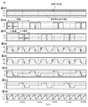
- FIG. 3 is a diagram illustrating operation waveforms of the power conversion device according to the first embodiment.
- FIG. 6 is a diagram illustrating a current path during operation according to the first embodiment.
- FIG. 6 is a diagram illustrating an output waveform of the filter circuit according to the first embodiment.
- FIG. 7 is a diagram illustrating another current path during operation according to the first embodiment.
- FIG. 6 is a circuit configuration diagram of a power conversion device according to a second embodiment.
- FIG. 11 is a diagram showing a duty relationship of a DC/AC converter in the power converter according to the third embodiment.
- FIG. 10 is a diagram showing operation waveforms of a switching operation of the power conversion device according to the third embodiment.
- FIG. 1 is a diagram showing a circuit configuration of a power conversion device according to a first embodiment.
- the DC voltage source 1 is input to the DC/AC converter 3 via the link capacitor 2.
- the DC/AC converter 3 includes a plurality of bridge-type inverters, which are DC/AC converters, and n inverters INV1 to INVn are connected in parallel.
- the inverter INV1 is composed of switching elements SW11 to SW14, and the inverter INVn is composed of switching elements SWn1 to SWn4.
- the AC outputs of the inverters INV1 to INVn forming the DC/AC converter 3 are formed by winding a plurality of (n in this example) primary windings and a plurality of secondary windings (m in this example) on one core. And magnetically coupled to the primary windings 411 to 41n of the transformer 4, respectively.
- the plurality of secondary windings of the transformer 4 are composed of center taps.
- the first winding is the secondary windings 421a and 421b
- the m-th winding is the secondary windings 42ma and 42mb. To do.
- a rectifier circuit 5 having a common anode is connected to the secondary windings 421a, 421b to 42ma, 42mb, and a filter circuit 6 is connected to the output of the center tap.
- the details of the connection will be described by taking the first secondary windings 421a and 421b as an example.
- the cathodes of the rectifying elements 51a and 51b forming the rectifying circuit 5 are connected, and the center tap is formed.
- the smoothing reactor 61a of the filter circuit 6 is connected to the output, and the smoothing capacitor 61b is connected to the output of the smoothing reactor 61a.
- the output of the smoothing capacitor 61b is connected to the anodes of the rectifying elements 51a and 51b, the connection point of the smoothing reactor connected to the second secondary winding and the smoothing capacitor.
- the load 7 is connected to the connection point between the first smoothing reactor 61a and the smoothing capacitor 61b and the connection point between the m-th smoothing reactor 6ma and the smoothing capacitor 6mb.
- the control circuit 10 sets the voltage of the load 7 to a predetermined voltage based on the outputs of the input voltage sensor 8 and the output voltage sensor 9, the phase of the inverter group forming the DC/AC converter 3 is n phase. Then, the duty control of each inverter is performed (interleave drive control).
- the storage device 101 includes a volatile storage device such as a random access memory and a non-volatile auxiliary storage device such as a flash memory, which are configured by the processor 100 and the storage device 101. Further, an auxiliary storage device such as a hard disk may be provided instead of the flash memory.
- the processor 100 executes the program input from the storage device 101, and performs a part or all of interleave drive control or switching between interleave drive and in-phase drive described later. In this case, the program is input to the processor 100 from the auxiliary storage device via the volatile storage device.
- the processor 100 may output data such as a calculation result to the volatile storage device of the storage device 101, or may store the data in the auxiliary storage device via the volatile storage device. Further, in addition to the processor 100 and the storage device 101, a logic circuit or an analog circuit may be used together.
- FIG. 3A shows the voltage of the DC voltage source 1 and the voltage of the load 7, which is an output, and the voltage of the DC voltage source 1 is 400V, and the voltage of the load 7 is about 420V in a step-up relationship.
- FIG. 3B shows the drive timing of the inverter INV1 of the DC/AC converter 3, and shows the operation timing of the switching elements SW11, SW13 of the upper arm on the bridge side.
- FIG. 3C shows the drive timing of the inverter INV2 of the DC/AC converter 3, and shows the operation timing of the switching elements SW21, SW23 of the upper arm on the bridge side.
- the inverter INV1 and the inverter INV2 are divided into two in one cycle and are operated with a phase shift of 180 degrees.
- the number of inverters is N phases
- one cycle is divided into n, and 360 degrees/n phases are shifted to drive each interleaved.
- FIG. 3D shows the voltage of the primary winding 411 of the transformer 4
- FIG. 3E shows the voltage of the primary winding 412 of the transformer 4.
- the inverter INV1 is turned on/off only in a half cycle within one cycle to generate a voltage in the primary winding 411 of the transformer 4, and the inverter INV1 is not turned on/off in the 2/2 cycle.
- the primary winding 411 and the primary winding 412 of the transformer 4 are coupled, a voltage is generated in the primary winding 411 of the transformer 4 even in the 2/2 cycle in which the inverter INV2 operates.
- the inverter INV2 is turned on/off only in the 2/2 cycle within one cycle to generate a voltage in the primary winding 412 of the transformer 4, and the 1/2 cycle of the inverter INV2 is turned on/off.
- the primary winding 411 and the primary winding 412 of the transformer 4 are coupled, a voltage is generated in the primary winding 412 of the transformer 4 even in the 1/2 cycle in which the inverter INV1 operates.
- a voltage is generated in the primary windings 411 and 412 of the transformer 4 even when the switching is not performed.
- the inverter INV2 does not perform the rectifying operation to draw the load current into the DC voltage source 1, and the power from the DC voltage source 1 passes through the secondary windings 421a, 421b, 422a, 422b of the transformer 4 and is applied to the load 7. Transmitted.
- the drive frequency of the transformer 4 can be doubled the drive frequency of the inverters INV1 and INV2. That is, since one cycle is time-divided by the inverter two phases and the voltage is alternately applied to the transformer 4, the VT product (V is the applied voltage, T is the time during which the voltage is applied to the primary winding) is half. Therefore, the core of the transformer 4 can be made smaller. Therefore, it is not necessary to increase the drive frequency of the inverters INV1 and INV2 in order to reduce the core of the transformer 4, and the switching loss can be reduced. Similarly, when the n-phase inverters are alternately operated, the VT product becomes 1/n, and the core of the transformer 4 can be further downsized.
- FIG. 3F shows the current in the primary winding 411 of the transformer 4
- FIG. 3G shows the current in the primary winding 412 of the transformer 4.
- the current flows only in the 1/2 cycle in which the inverter INV1 is operating (the timing shown in FIG. 3B), and in FIG. 3G, only in the 2/2 cycle in which the inverter INV2 is operating (the timing shown in FIG. 3C).
- the inverter is composed of n-phases, the current application time becomes 1/n, and by making the phases multi-phase, the average current and effective current value per inverter can be reduced and the copper loss of the inverter can be reduced. Therefore, the loss of the DC/AC converter 3 can be reduced.
- FIG. 3H shows the current flowing through the smoothing reactor 61a, and the ripple frequency of the current is 2n times the switching frequency of the inverter forming the DC/AC converter 3 (4 times when the inverter has two phases), and the current ripple is small.
- the current ripple frequency can be increased, the capacities of the smoothing reactors 61a to 6ma and the smoothing capacitors 61b to 6mb of the filter circuit 6 can be reduced.
- FIG. 4 shows a current path when the switching element SW11 and the switching element SW14 of the inverter INV1 are on.
- the current on the primary side of the transformer 4 serves as a path for obtaining the switching element SW11, the primary winding 411, and the switching element SW14 from the DC voltage source 1 and returning to the DC voltage source 1.
- a voltage is generated in the other primary windings of the transformer 4, but since the number of turns of the primary windings is the same, a voltage that does not constantly exceed the DC voltage source 1 does not occur, and the remaining inverters INV2 to INVn have load currents. Does not flow.
- a voltage corresponding to the turn ratio between the primary winding and the secondary winding of the transformer 4 is generated, and the rectifying elements 51b to 5mb in the rectifying circuit 5 are turned on.
- the filter circuits 6 connected to the respective secondary windings are connected in series, and a voltage that is m times the voltage per filtered stage is applied to the load 7.
- the impedance of the smoothing reactors 61a to 6ma of the filter circuit 6 is set to a value sufficiently lower than that of the load 7, the current including the current ripple is, for example, the secondary winding of the transformer 4 as shown by the dotted line in FIG.
- the current circulates through the line 421b, the smoothing reactor 61a, and the smoothing capacitor 61b, and only the DC component including the extremely small current ripple flows through the load 7.
- FIG. 5 shows current waveforms of the smoothing reactor 61a, the smoothing capacitor 61b, and the load 7 when two-phase parallel driving is performed using the inverters INV1 and INV2.
- 5A shows the input/output voltage of the power conversion device as in FIG. 3A
- FIG. 5B is the drive timing of the inverter INV1 as in FIG. 3B
- FIG. 5C is the drive timing of the inverter INV2 as in FIG. 3C
- FIG. 5E shows the current of the smoothing capacitor 61b.
- the frequency of the current ripple flowing in the smoothing reactor 61a is a current including a ripple component having a frequency four times as high as the switching frequency for driving the inverter INV1 and the inverter INV2, but the impedance of the smoothing capacitor 61b is made sufficiently small with respect to the load 7. If so, the current ripple component almost flows into the smoothing capacitor 61b, circulates in the secondary winding 421b of the transformer 4 and the smoothing reactor 61a, and does not appear in the load 7.
- FIG. 6 shows a current path when the switching element SW13 and the switching element SW12 of the inverter INV1 are on.
- the current on the primary side of the transformer 4 serves as a path for obtaining the switching element SW13, the primary winding 411, and the switching element SW12 from the DC voltage source 1 and returning to the DC voltage source 1.
- a voltage is generated in the other primary windings of the transformer 4, but since the number of turns of the primary windings is the same, a voltage that does not constantly exceed the DC voltage source 1 does not occur, and the remaining inverters INV2 to INVn have load currents. Does not flow.
- a voltage corresponding to the turn ratio between the primary winding and the secondary winding of the transformer 4 is generated, and the rectifying elements 51a to 5ma in the rectifier circuit 5 are turned on.
- the surge voltage can also be reduced.
- the current including the current ripple is, for example, the secondary winding 421b of the transformer 4 as shown by the dotted line in the figure.
- the description of the current is omitted because it is the same as that described in FIG. 5 except that the secondary winding of the transformer flows.
- the power conversion device has the following effects, and can realize a high output, high voltage power supply with low loss and a small size.
- the driving frequency of the transformer can be set to N times the driving frequency of the DC/AC converter, so that the VT product of the transformer is reduced and the core can be downsized.
- the current application time of the DC/AC converter can be dispersed to 1/N, copper loss is small.
- the rectified voltage is connected in series to obtain the output voltage, so the rectified voltage per stage is small, so the surge voltage is small, the loss is reduced without the surge circuit, and the rectifier circuit is inexpensive and has a low withstand voltage.
- a high voltage output circuit can be configured with the elements. (5) Since the phase of the DC/AC converter is shifted and the interleave operation is performed, the output current ripple becomes high frequency and small, and the filter circuit can be downsized.
- Embodiment 2 In the first embodiment, the configuration of the secondary side of the transformer 4 is connected in series with the outputs of the individual filters in the filter circuit 6 to output a high voltage to the load 7, but in the second embodiment, the rectification is performed. The output of the circuit 5 is connected in series to generate a high voltage to the load 7.
- the configuration of the second embodiment will be described with reference to FIG.
- the configuration of the primary windings 411 to 41n of the transformer 4 is the same as that of the first embodiment, and therefore will be omitted.
- the anodes of the rectifying elements 51a and 51b forming the rectifying circuit 5 are connected, and this is connected to the center tap point of the secondary winding of the transformer 4 of the next stage.
- the same connection is repeated a total of m-1 times to connect m-stage rectifier circuits in series. Note that, in FIG. 7, the rectifier circuit between the first stage rectifier circuit including the rectifier elements 51a and 51b and the mth stage rectifier circuit including the rectifier elements 5ma and 5mb is omitted.
- the smoothing reactor 61a is connected to the connection point between the center tap point of the secondary windings 421a and 421b of the first stage and the anode of the rectifying elements 5ma and 5mb of the m stage, which are the output ends of the rectifying circuit 5 connected in series. And the smoothing capacitor 61b are connected to the filter circuit 6, and the output of the filter circuit 6 is connected to the load 7.
- the voltage across the smoothing reactor 61a that constitutes the filter circuit 6 becomes high, so that the current ripple flowing through the smoothing reactor 61a and the smoothing capacitor 61b becomes large. Since the number of smoothing reactors and smoothing capacitors can be reduced compared to the above, the power converter can be further downsized. That is, although the current ripple increases as compared with the first embodiment, the filter circuit 6 becomes smaller and the other effects are the same as those of the first embodiment.
- Embodiment 3 The power conversion device according to the third embodiment has the same configuration as that of the first or second embodiment, and the interleave drive that operates by shifting the phases of the inverters INV1 to INVn forming the DC/AC converter 3 and the inverter INV1.
- the so-called in-phase drive in which the to INVn are operated in the same phase is switched and operated according to the voltage of the DC voltage source 1.
- the load 7 is a rechargeable battery or the like, and the relationship between the load voltage when charging proceeds and the duty of the inverters INV1 to INVn forming the DC/AC converter 3 is shown in FIG.
- the voltage Vin of the DC voltage source 1 is constant, the voltage of the load 7 is low at the initial stage of charging, and therefore the DC/AC converter 3 reduces the duty based on the instruction of the control circuit 10 and the average voltage of the secondary side of the transformer 4. Adjust and charge.
- the control circuit 10 raises the average voltage on the secondary side of the transformer 4, so that the DC/AC converter 3 widens the duty to perform the charging operation (graph P). ..
- the duty of the DC/AC converter 3 is maximized so that the transformer 4 has a high operation ratio, that is, the so-called effective current value is low. It is desired to perform maximum duty control such that charging is performed while changing the voltage Vin (graph Q).
- the maximum duty control in the initial charging state, the voltage of the DC voltage source 1 is low and the VT product has a margin (for example, the period R), the DC/AC converter 3 is interleaved, and the drive frequency of the transformer 4 is increased. If this is left high, iron loss will be wasted.
- the operation of the DC/AC converter 3 is reduced to the in-phase drive or the interleave drive of the interleave drive. By switching, the iron loss can be suppressed and the power conversion device can be operated with high efficiency.
- FIG. 9 illustrates the switching timing between the drive timings, the duty, the interleave and the in-phase drive of the inverters INV1 and INV2 when the DC/AC converter 3 is driven in two phases in parallel using the inverters INV1 and INV2.
- FIG. 9A schematically shows the drive timing and duty of each of the interleaved inverters INV1 and INV2 during the initial charging when the voltage Vin of the DC voltage source 1 is fixed.
- the charge voltage of the load 7 is low, so the duty is reduced so that the secondary side average voltage of the transformer 4 is reduced, and power is transmitted to the secondary side of the transformer 4 during this short operation period. Therefore, the effective current value is high and the loss is large.
- FIG. 9B schematically shows the driving timing and duty of each of the interleaved inverters INV1 and INV2 when charging is completed. Since the charging voltage of the load 7 is high, in order to increase the secondary side average voltage of the transformer 4, the duty is wide and the effective current value is suppressed to be low, so that the operation is highly efficient.
- the constant duty control is control in which the input voltage Vin of the DC voltage source 1 is variable so that the duty becomes large. Since the input voltage Vin is variable, the number of interleave drives is variable.
- FIG. 9C shows a case where the DC/AC converter 3 is driven in phase when the voltage of the DC voltage source 1 at the initial stage of charging is low and the duty is maximized so that the core of the transformer 4 has a VT product that does not saturate.
- the drive frequency of the transformer 4 is the same as the switching frequency of the inverters INV1 and INV2, and the frequency is lower than that during interleave drive, so that iron loss can be reduced.
- the operation frequency of the DC/AC converter 3 can be changed according to the voltage of the DC voltage source 1 by changing the number of interleave drives or switching between interleave drive and in-phase drive. By doing so, it is possible to obtain a power converter that is compatible with high power and high output voltage and that can reduce the size of the transformer and reduce the loss.
Landscapes
- Engineering & Computer Science (AREA)
- Power Engineering (AREA)
- Dc-Dc Converters (AREA)
Abstract
電力変換装置の高電圧高出力化とトランスの小型低損失化を目的とし、一つのコアで構成された複数の巻線をもつトランス(4)を用い、複数のインバータ(INV1~INVn)の出力を一次側巻線(411~41n)に並列接続し、二次側巻線(421a、421b~42ma、42mb)を整流後に直列に接続し、入力電圧に応じてインバータ(INV1~INVn)のインターリーブ駆動数を変えるか、もしくはインターリーブと同相駆動とを切り替えて動作させる。
Description
本願は、電力変換装置に関するものである。
例えば、高電圧を要する装置として、X線CT装置およびX線撮影装置があり、これらは、X線管から発生したX線を被検体に照射し、被検体を透過したX線量を検出して画像化するものである。このような装置では、X線管のアノード・カソード間に直流高電圧を印加し、カソードを高温にすることにより発生する熱電子を高電圧で加速し、これをカソードに衝突させてX線を発生させている。
この高電圧を得るため、例えば特許文献1に示されるように、インバータの出力を並列接続されたトランスに接続し、トランス出力を整流後に直列に接続し、負荷の電極に高電圧を得るような構成が取られている。
また、特許文献2に示されるように、複数の電源線から入力される入力電圧のバラツキを吸収しつつトランスを小型化するために、LC共振回路を設け、1つのコアで磁気的に結合した複数のトランスを有するスイッチング電源装置が示されている。
また、特許文献2に示されるように、複数の電源線から入力される入力電圧のバラツキを吸収しつつトランスを小型化するために、LC共振回路を設け、1つのコアで磁気的に結合した複数のトランスを有するスイッチング電源装置が示されている。
特許文献1に示す電源装置は、並列接続されたトランスにインバータの出力を接続し、トランス出力を整流後に直列に接続し、負荷の電極に高電圧を得るような構成が示されている。しかしながら、トランスを小型化する考えが示されていない。
特許文献2の構成では、複数のトランスをひとつのコアに磁気統合し、二次側に高電圧を得る回路と、磁気統合をすることでトランスを小型化する考えが示されているが、その磁気統合したトランスを、さらに小型化する考えが示されていない。
また、特許文献1、特許文献2とも、電力変換装置の低損失化、大電力化、または出力電圧の高電圧化時に問題となるサージ抑制方法について記載がない。
また、特許文献1、特許文献2とも、電力変換装置の低損失化、大電力化、または出力電圧の高電圧化時に問題となるサージ抑制方法について記載がない。
本願は、上記のような問題点を解消するために成されたものであって、電力変換装置の低損失化により大電力化を可能とし、サージを抑制して高電圧出力を可能とし、トランスを小型化できる電力変換装置の提供を目的とする。
本願に開示される電力変換装置は、
直流電源を交流変換するためのN個(Nは2以上の整数)のDC/AC変換部、
N個のDC/AC変換部のそれぞれに接続されるN個の一次巻線とN個の一次巻線と磁気的に結合するM個(Mは2以上の整数)の二次巻線とを有するトランス、
トランスに接続され、トランスからの出力を直流に整流して出力するM個の整流回路、
DC/AC変換部を制御する制御回路、
を備え、
M個の整流回路の直流側端子は互いに接続されており、
制御回路は、N個のDC/AC変換部を、位相をずらしたインターリーブ駆動させること、を特徴とする。
直流電源を交流変換するためのN個(Nは2以上の整数)のDC/AC変換部、
N個のDC/AC変換部のそれぞれに接続されるN個の一次巻線とN個の一次巻線と磁気的に結合するM個(Mは2以上の整数)の二次巻線とを有するトランス、
トランスに接続され、トランスからの出力を直流に整流して出力するM個の整流回路、
DC/AC変換部を制御する制御回路、
を備え、
M個の整流回路の直流側端子は互いに接続されており、
制御回路は、N個のDC/AC変換部を、位相をずらしたインターリーブ駆動させること、を特徴とする。
また、本願に開示される電力変換装置は、
一つのコアにN個(Nは2以上の整数)の一次巻線とM個(Mは2以上の整数)の二次巻線を巻回して構成されるトランス、
N個の一次巻線に接続され、直流電源を交流変換するN個のDC/AC変換部、
入力側はM個の二次巻線に接続され、トランスからの出力を直流に整流して出力するM個の整流回路、
DC/AC変換部を制御する制御回路、
を備え、
制御回路は、N個のDC/AC変換部を、互いに位相をずらしたインターリーブ駆動と同相駆動とを直流電源の電圧に応じて切替えることを特徴とする。
一つのコアにN個(Nは2以上の整数)の一次巻線とM個(Mは2以上の整数)の二次巻線を巻回して構成されるトランス、
N個の一次巻線に接続され、直流電源を交流変換するN個のDC/AC変換部、
入力側はM個の二次巻線に接続され、トランスからの出力を直流に整流して出力するM個の整流回路、
DC/AC変換部を制御する制御回路、
を備え、
制御回路は、N個のDC/AC変換部を、互いに位相をずらしたインターリーブ駆動と同相駆動とを直流電源の電圧に応じて切替えることを特徴とする。
DC/AC変換部の位相をずらして動作させるため、トランスをDC/AC変換部のスイッチング周波数以上の周波数で駆動できることになり、DC/AC変換部器のスイッチング周波数を上げることなくトランスのコアを小型化できる。
また、入力電圧に応じてインターリーブ駆動と同相駆動を切替えることにより、鉄損を低下させることができる。
また、入力電圧に応じてインターリーブ駆動と同相駆動を切替えることにより、鉄損を低下させることができる。
以下、本願に係る電力変換装置の好適な実施の形態について、図面を参照して説明する。なお、同一内容および相当部については同一符号を配し、その詳しい説明は省略する。以降の実施形態も同様に、同一符号を付した構成について重複した説明は省略する。
実施の形態1.
図1は、実施の形態1による電力変換装置の回路構成を示した図である。図1に示すように、直流電圧源1はリンクコンデンサ2を経て、DC/AC変換器3に入力される。DC/AC変換器3は、DC/AC変換部であるブリッジ型インバータが複数で構成され、インバータINV1~INVnまでのn個を並列接続した構成である。インバータINV1は、スイッチング素子SW11~SW14で構成され、インバータINVnは、スイッチング素子SWn1~SWn4で構成される。
図1は、実施の形態1による電力変換装置の回路構成を示した図である。図1に示すように、直流電圧源1はリンクコンデンサ2を経て、DC/AC変換器3に入力される。DC/AC変換器3は、DC/AC変換部であるブリッジ型インバータが複数で構成され、インバータINV1~INVnまでのn個を並列接続した構成である。インバータINV1は、スイッチング素子SW11~SW14で構成され、インバータINVnは、スイッチング素子SWn1~SWn4で構成される。
DC/AC変換器3を構成するインバータINV1~INVnのAC出力は、複数(この例ではn個)の一次巻線と複数の二次巻線(この例ではm個)を一つのコアに巻いて磁気結合したトランス4の一次巻線411~41nにそれぞれ接続される。トランス4の複数の二次巻線はセンタータップで構成されており、一つ目の巻線を、二次巻線421a、421b、m個目の巻線を、二次巻線42ma、42mbとする。
この二次巻線421a、421b~42ma、42mbにはアノードを共通とした整流回路5が接続され、センタータップの出力にフィルタ回路6が接続される。
一つ目の二次巻線421a、421bを例に接続の詳細を説明すると、二次巻線421a、421bには、整流回路5を構成する整流素子51aと51bのカソードが接続され、センタータップ出力にフィルタ回路6の平滑リアクトル61aが接続され、平滑リアクトル61aの出力には平滑コンデンサ61bが接続される。
平滑コンデンサ61bの出力は、整流素子51a、51bのアノードと、2個目の二次巻線に接続される平滑リアクトルと平滑コンデンサの接続点に接続される。これらの接続をトランス4に設けたm個の二次巻線とm個の整流回路を繰り返して接続することにより、m個の直流側端子は互いに接続される。一つ目の平滑リアクトル61aと平滑コンデンサ61bの接続点と、m個目の平滑リアクトル6maと平滑コンデンサ6mbの接続点に負荷7が接続される。
制御回路10は、入力電圧センサ8と、出力電圧センサ9の出力をもとに、負荷7の電圧を所定の電圧とするため、DC/AC変換器3を構成するインバータ群の位相をn相にずらして、それぞれのインバータのデューティ制御を行う(インターリーブ駆動制御)。
制御回路10のハードウエアの一例を図2に示す。プロセッサ100と記憶装置101から構成され、図示していないが、記憶装置101はランダムアクセスメモリ等の揮発性記憶装置と、フラッシュメモリ等の不揮発性の補助記憶装置とを具備する。また、フラッシュメモリの代わりにハードディスクの補助記憶装置を具備してもよい。プロセッサ100は、記憶装置101から入力されたプログラムを実行し、インターリーブ駆動制御または後述するインターリーブ駆動と同相駆動との切替えの一部又は全部を遂行する。この場合、補助記憶装置から揮発性記憶装置を介してプロセッサ100にプログラムが入力される。また、プロセッサ100は、演算結果等のデータを記憶装置101の揮発性記憶装置に出力してもよいし、揮発性記憶装置を介して補助記憶装置にデータを保存してもよい。また、プロセッサ100及び記憶装置101に加え、ロジック回路、アナログ回路を併用してもよい。
図1で説明した、DC/AC変換器3のインバータINV1、INV2(n=2)、トランス4の一次巻線411、412(n=2)、トランス4の二次巻線421a、421b、422a、422b(m=2)とした場合の各部の動作波形について図3を用いて説明する。
図3Aは直流電圧源1の電圧と、出力である負荷7の電圧を示しており、直流電圧源1の電圧が400V、負荷7の電圧が420V程度の昇圧関係となっている。
図3BはDC/AC変換器3のインバータINV1の駆動タイミングを示しており、ブリッジ側の上アームのスイッチング素子SW11、SW13の動作タイミングを示す。
図3CはDC/AC変換器3のインバータINV2の駆動タイミングを示しており、ブリッジ側の上アームのスイッチング素子SW21、SW23の動作タイミングを示す。
図3B、図3Cからわかるように、インバータINV1とインバータINV2は一周期内を2分割し、180度位相をずらして動作させている。インバータの数がN相ある場合は、一周期をn分割し、360度/n位相をずらしてそれぞれをインターリーブ駆動させる。
図3BはDC/AC変換器3のインバータINV1の駆動タイミングを示しており、ブリッジ側の上アームのスイッチング素子SW11、SW13の動作タイミングを示す。
図3CはDC/AC変換器3のインバータINV2の駆動タイミングを示しており、ブリッジ側の上アームのスイッチング素子SW21、SW23の動作タイミングを示す。
図3B、図3Cからわかるように、インバータINV1とインバータINV2は一周期内を2分割し、180度位相をずらして動作させている。インバータの数がN相ある場合は、一周期をn分割し、360度/n位相をずらしてそれぞれをインターリーブ駆動させる。
図3Dはトランス4の一次巻線411の電圧、図3Eはトランス4の一次巻線412の電圧を示す。図3Dの場合、インバータINV1は1周期内の1/2周期にのみオン・オフ動作をしてトランス4の一次巻線411に電圧が生じ、インバータINV1の2/2周期はオン・オフ動作しないが、トランス4の一次巻線411と一次巻線412が結合しているため、インバータINV2が動作する2/2周期においてもトランス4の一次巻線411に電圧が生じることになる。
図3Eの場合も同様、インバータINV2は1周期内の2/2周期にのみオン・オフ動作をしてトランス4の一次巻線412に電圧が生じ、インバータINV2の1/2周期はオン・オフ動作をしないが、トランス4の一次巻線411と一次巻線412が結合しているため、インバータINV1が動作する1/2周期においてもトランス4の一次巻線412に電圧が生じることになる。
このように、トランス4の一次巻線411、412には、スイッチングしない時にも電圧が生じるが、一次巻線411、412の巻数を同じにしておけば、例えばインバータINV1が動作している時に、インバータINV2が整流動作をして直流電圧源1に負荷電流を引き込むことはなく、直流電圧源1からの電力は、トランス4の二次巻線421a、421b、422a、422bを通って負荷7に伝送される。
以上のように、インバータINV1、INV2で180度位相を交互にずらしたインターリーブ駆動のスイッチングを行うと、トランス4の駆動周波数をインバータINV1、INV2の駆動周波数の2倍にできる。すなわち、1周期をインバータ2相で時分割してトランス4に対して交互に電圧を印加するのでVT積(Vは印加電圧、Tは1次巻線に電圧を印加している時間)が半分となり、トランス4のコアを小さくできる。従って、トランス4のコアを小さくするために、インバータINV1、INV2の駆動周波数を高くする必要がなく、スイッチング損失を小さくすることができる。
同様に、n相のインバータで交互に動作をさせるとVT積が1/nとなりトランス4のコアのさらなる小型化が可能になる。
同様に、n相のインバータで交互に動作をさせるとVT積が1/nとなりトランス4のコアのさらなる小型化が可能になる。
図3Fはトランス4の一次巻線411の電流、図3Gはトランス4の一次巻線412の電流を示す。図3FはインバータINV1が動作している1/2周期にのみ(図3Bで示すタイミング)電流が流れ、図3GはインバータINV2が動作している2/2周期にのみ(図3Cで示すタイミング)で電流が流れることを示す。すなわち、インバータを2相で動かすと、電流の印加時間が半分になっていることがわかる。
従って、インバータをn相で構成すると電流印加時間は1/nとなり、多相化することにより、インバータあたりの平均電流および電流実効値を減らすことができ、インバータの銅損を低減できることになる。従って、DC/AC変換器3の低損失化が実現できる。
従って、インバータをn相で構成すると電流印加時間は1/nとなり、多相化することにより、インバータあたりの平均電流および電流実効値を減らすことができ、インバータの銅損を低減できることになる。従って、DC/AC変換器3の低損失化が実現できる。
図3Hは平滑リアクトル61aを流れる電流であり、電流のリプル周波数がDC/AC変換器3を構成するインバータのスイッチング周波数の2n倍(インバータが2相の場合では4倍)となり、電流リプルが小さいことと、電流リプル周波数を高くできるため、フィルタ回路6の平滑リアクトル61a~6maと平滑コンデンサ61b~6mbの容量を小さくすることができる。
次に電力変換装置の動作について説明する。図4はインバータINV1のスイッチング素子SW11とスイッチング素子SW14がオンしている時の電流経路を示している。トランス4の一次側の電流は、直流電圧源1から、スイッチング素子SW11、一次巻線411、スイッチング素子SW14を得て、直流電圧源1に戻る経路となる。トランス4のその他の1次巻線には電圧が生じるが、一次巻線の巻数を同数としているため、定常的に直流電圧源1を上回る電圧が生じず、残りのインバータINV2~INVnに負荷電流が流れることはない。
トランス4の二次巻線421a、421b~42ma、42mbにはトランス4の一次巻線と二次巻線の巻数比に応じた電圧が生じ、整流回路5内の整流素子51b~5mbが導通し、センタータップ点から平滑リアクトル61a~6maに向かって電流が流れる。2次巻線のそれぞれに接続されたフィルタ回路6は直列接続されており、負荷7には、フィルタ後の1段あたりの電圧のm倍の電圧が印加される。
フィルタ回路6の平滑リアクトル61a~6maのインピーダンスを負荷7に比べて十分低い値に設定すると、電流リプルを含んだ電流は、図4中点線で示したように、例えば、トランス4の二次巻線421b、平滑リアクトル61a、平滑コンデンサ61bを循環する電流となり、負荷7にはきわめて小さな電流リプル含んだ直流成分のみが流れる。
図5にインバータINV1、INV2を用いて2相並列駆動をした場合の、平滑リアクトル61a、平滑コンデンサ61b、負荷7の電流波形を示す。
図5Aは、図3A同様、電力変換装置の入出力電圧を示し、図5Bは、図3B同様、インバータINV1の駆動タイミング、図5Cは、図3C同様、インバータINV2の駆動タイミング、図5Dは、図3H同様、平滑リアクトル61aと、負荷7の電流を示し、図5Eは平滑コンデンサ61bの電流を示す。
平滑リアクトル61aに流れる電流リプルの周波数はインバータINV1およびインバータINV2を駆動するスイッチング周波数の4倍の周波数のリプル成分を含んだ電流が流れるが、平滑コンデンサ61bのインピーダンスを負荷7に対して十分小さくしておけば、この電流リプル成分は、平滑コンデンサ61bにほぼ流れこんでトランス4の二次巻線421b、平滑リアクトル61aを循環し、負荷7には現れない。
次に、図6にインバータINV1のスイッチング素子SW13とスイッチング素子SW12がオンしている時の電流経路を示す。トランス4の一次側の電流は、直流電圧源1から、スイッチング素子SW13、一次巻線411、スイッチング素子SW12を得て、直流電圧源1に戻る経路となる。トランス4のその他の1次巻線には電圧が生じるが、一次巻線の巻数を同数としているため、定常的に直流電圧源1を上回る電圧が生じず、残りのインバータINV2~INVnに負荷電流が流れることはない。
トランス4の二次巻線421a、421b~42ma、42mbにはトランス4の一次巻線と二次巻線の巻数比に応じた電圧が生じ、整流回路5内の整流素子51a~5maが導通し、センタータップ点から平滑リアクトル61a~6maに向かって電流が流れ、直列接続されたフィルタ回路6により、負荷7には、フィルタ後の1段あたりの電圧のm倍の電圧が印加される。また、整流回路5内のそれぞれの整流素子51a~5maにかかる電圧を小さくできるため、サージ電圧も小さくすることができる。
フィルタ回路の平滑リアクトル61a~6maのインピーダンスを負荷7に比べて十分低い値に設定すると、電流リプルを含んだ電流は、図中点線で示したように、例えば、トランス4の二次巻線421b、平滑リアクトル61a、平滑コンデンサ61bを循環する電流となり、負荷7にはきわめて小さな電流リプル含んだ直流成分のみが流れる。
電流の説明については、トランスの二次巻線の流れる箇所が異なるだけで図5にて説明した通りであるため割愛する。
電流の説明については、トランスの二次巻線の流れる箇所が異なるだけで図5にて説明した通りであるため割愛する。
DC/AC変換器3内の並列接続された他のインバータINV2~INVnの位相をずらして動作した時も上述と同様の電流経路と動作になる。
以上説明のように、本実施の形態の電力変換装置は、以下のような効果を奏し、高出力、高電圧電源が低損失かつ小型に実現することができる。
(1)位相をずらした場合はトランスの駆動周波数をDC/AC変換部の駆動周波数のN倍にできるため、トランスのVT積が小さくなり、コアを小型化できる。
(2)DC/AC変換部の電流印加時間を1/Nに分散できるため、銅損が小さい。
(3)トランスのコアを小さくするために、DC/AC変換部の駆動周波数を高くする必要がなくスイッチング損失が小さい。
(4)整流後の電圧を直列接続して出力電圧を得るため、1段あたりの整流電圧が小さいため、サージ電圧が小さくなり、サージ回路レスによる低損失化、および整流回路が安価な低耐圧素子で高電圧出力の回路が構成できる。
(5)DC/AC変換部の位相をずらしてインターリーブ動作させるため、出力電流リプルが高周波化されて小さくなり、フィルタ回路が小型化できる。
実施の形態2.
実施の形態1は、トランス4の二次側の構成をフィルタ回路6内の個々のフィルタの出力を直列に接続して、負荷7へ高電圧を出力させていたが、実施の形態2は整流回路5の出力を直列接続して負荷7へ高電圧を発生させる構成としたものである。
実施の形態1は、トランス4の二次側の構成をフィルタ回路6内の個々のフィルタの出力を直列に接続して、負荷7へ高電圧を出力させていたが、実施の形態2は整流回路5の出力を直列接続して負荷7へ高電圧を発生させる構成としたものである。
実施の形態2の構成について図7を用いて説明する。トランス4の一次巻線411~41nの構成については実施の形態1と同じであるため割愛する。整流回路5を構成する整流素子51aと51bのアノードを接続し、これを次段のトランス4の二次巻線のセンタータップ点に接続する。同様の接続を合計m-1回繰り返して接続して、m段の整流回路の直列接続を行う。なお、図7では、整流素子51a、51bからなる1段目の整流回路と、整流素子5ma、5mbからなるm段目の整流回路との間にある整流回路は省略している。
この直列に接続された整流回路5の出力端である、1段目の二次巻線421a、421bのセンタータップ点と、m段目の整流素子5ma、5mbのアノードの接続点に平滑リアクトル61aと平滑コンデンサ61bからなるフィルタ回路6を接続し、フィルタ回路6の出力に負荷7を接続している。
このような構成により、フィルタ回路6を構成する、平滑リアクトル61aの両端電圧が高くなるため、平滑リアクトル61a、および平滑コンデンサ61bに流れる電流リプルが大きくなるが、これを許容できれば、実施の形態1に比較して、平滑リアクトルと平滑コンデンサの数を減らすことができるので、電力変換装置のさらなる小型化が可能となる。すなわち、電流リプルが実施の形態1に比べて増加はするが、フィルタ回路6は小さくなり、その他の効果については実施の形態1と同じ効果が得られる。
実施の形態3.
実施の形態3の電力変換装置は、実施の形態1または実施の形態2と同構成で、DC/AC変換器3を構成するインバータINV1~INVnの位相をずらして動作させるインターリーブ駆動と、インバータINV1~INVnを同じ位相で動作させるいわゆる同相駆動とを、直流電圧源1の電圧に応じて、切り替えて動作するものである。
実施の形態3の電力変換装置は、実施の形態1または実施の形態2と同構成で、DC/AC変換器3を構成するインバータINV1~INVnの位相をずらして動作させるインターリーブ駆動と、インバータINV1~INVnを同じ位相で動作させるいわゆる同相駆動とを、直流電圧源1の電圧に応じて、切り替えて動作するものである。
負荷7が充電池等であり、充電が進む時の負荷電圧と、DC/AC変換器3を構成するインバータINV1~INVnのデューティの関係を図8に示す。
直流電圧源1の電圧Vinが一定の場合、充電初期は負荷7の電圧が低いため、DC/AC変換器3は制御回路10の指令に基づきデューティを絞ってトランス4の二次側の平均電圧を調整して充電する。充電が進み、負荷7の充電電圧が高くなると、制御回路10はトランス4の二次側の平均電圧を高くするため、DC/AC変換器3はデューティを広げて充電動作をさせる(グラフP)。
直流電圧源1の電圧Vinが一定の場合、充電初期は負荷7の電圧が低いため、DC/AC変換器3は制御回路10の指令に基づきデューティを絞ってトランス4の二次側の平均電圧を調整して充電する。充電が進み、負荷7の充電電圧が高くなると、制御回路10はトランス4の二次側の平均電圧を高くするため、DC/AC変換器3はデューティを広げて充電動作をさせる(グラフP)。
一般にトランス4の動作比率が高い、いわゆる電流実効値が低くなるように、DC/AC変換器3のデューティを最大として、動作させたほうが電力変換装置の効率は良くなるため、直流電圧源1の電圧Vinを可変しながら充電するようなデューティ最大制御をさせることが望まれる(グラフQ)。このデューティ最大制御は、充電初期状態は直流電圧源1の電圧が低く、VT積に余裕がある状態(例えば期間R)で、DC/AC変換器3をインターリーブ動作させて、トランス4の駆動周波数が高いままにしておくと、鉄損を無駄に発生させることになる。このため、直流電圧源1の電圧を低い状態(期間R)では、DC/AC変換器3のインターリーブ駆動するインバータの数(インターリーブ駆動数)を減らし、究極は同相駆動にするとトランス4を駆動する周波数を下げることができる。
トランスが飽和しないVT積の条件、かつトランスの駆動周波数を下げると鉄損が下がる条件を満たす時刻t1で、DC/AC変換器3の動作を、インターリーブ駆動のインターリーブ数を下げる、もしくは同相駆動に切り替えると、鉄損を抑え電力変換装置を高効率に動作させることができる。
図9にDC/AC変換器3をインバータINV1、INV2を用いて2相並列駆動をした場合のインバータINV1、INV2の駆動タイミング、デューティ、インターリーブと同相駆動との切替え動作について説明する。
図9Aは直流電圧源1の電圧Vinを固定した時の、充電初期時のインターリーブ駆動のインバータINV1、2それぞれの駆動タイミングとデューティを模式的に記したものである。充電初期時は、負荷7の充電電圧が低いため、トランス4の二次側平均電圧を下げるようにデューティを絞った動作となっており、この短い動作期間においてトランス4の二次側に電力伝送を行うため、電流実効値が高く損失が大きい。
図9Bは、充電完了時のインターリーブ駆動のインバータINV1、INV2それぞれの駆動タイミングとデューティを模式的に記したものである。負荷7の充電電圧が高いため、トランス4の二次側平均電圧を上げるために、デューティが広く、電流実効値が低く抑えられ高効率動作とする。デューティ一定制御とは、このデューティが大きい状態となるよう、直流電圧源1の入力電圧Vinを可変とする制御である。入力電圧Vinを可変とするため、インターリーブ駆動数を可変とする。
図9Cは、充電初期の直流電圧源1の電圧が低く、デューティを最大となるように開き、トランス4のコアが飽和しないVT積となる場合に、DC/AC変換器3を同相駆動した時の図である。この場合はトランス4の駆動周波数がインバータINV1、INV2のスイッチング周波数と同じとなり、インターリーブ駆動時より周波数が下がるため、鉄損を小さくすることができる。
以上のように、直流電圧源1の電圧に応じて、DC/AC変換器3の動作を、インターリーブの駆動数の切り替え、またはインターリーブ駆動と同相駆動との切替えにより、トランス4の駆動周波数を可変とすることで、大電力、高出力電圧に対応した、トランスの小型化と低損失化が可能な電力変換器を得ることが出来る。
本願は、様々な例示的な実施の形態及び実施例が記載されているが、1つ、または複数の実施の形態に記載された様々な特徴、態様、及び機能は特定の実施の形態の適用に限られるのではなく、単独で、または様々な組み合わせで実施の形態に適用可能である。
従って、例示されていない無数の変形例が、本願明細書に開示される技術の範囲内において想定される。例えば、少なくとも1つの構成要素を変形する場合、追加する場合または省略する場合、さらには、少なくとも1つの構成要素を抽出し、他の実施の形態の構成要素と組み合わせる場合が含まれるものとする。
従って、例示されていない無数の変形例が、本願明細書に開示される技術の範囲内において想定される。例えば、少なくとも1つの構成要素を変形する場合、追加する場合または省略する場合、さらには、少なくとも1つの構成要素を抽出し、他の実施の形態の構成要素と組み合わせる場合が含まれるものとする。
1:直流電圧源、2:リンクコンデンサ、3:DC/AC変換器、INV1~INVn:インバータ、SW11~SWn4:半導体スイッチ、4:トランス、411~41n:一次巻線、421a、421b~42ma、42mb:二次巻線、5:整流回路、51a、51b~5ma、5mb:整流素子、6:フィルタ回路、61a~6ma:平滑リアクトル、61b~6mb:平滑コンデンサ、7:負荷、8:入力電圧センサ、9:出力電圧センサ、10:制御回路
Claims (10)
- 直流電源を交流変換するためのN個(Nは2以上の整数)のDC/AC変換部、
前記N個のDC/AC変換部のそれぞれに接続されるN個の一次巻線と前記N個の一次巻線と磁気的に結合するM個(Mは2以上の整数)の二次巻線とを有するトランス、
前記トランスに接続され、前記トランスからの出力を直流に整流して出力するM個の整流回路、
前記DC/AC変換部を制御する制御回路、
を備え、
前記M個の整流回路の直流側端子は互いに接続されており、
前記制御回路は、前記N個のDC/AC変換部を、位相をずらしたインターリーブ駆動させること、を特徴とする電力変換装置。 - 前記M個の整流回路は、M個のフィルタ回路を介して接続されており、前記M個のフィルタ回路は互いに直列に接続されていることを特徴とする請求項1に記載の電力変換装置。
- 前記M個の整流回路は、互いに直列に接続されており、前記直列に接続されたM個の整流回路の両端はフィルタ回路を介して負荷に接続されることを特徴とする請求項1に記載の電力変換装置。
- 前記インターリーブ駆動は、前記直流電源の電圧に応じて、前記DC/AC変換部のインターリーブ駆動数を可変とすることを特徴とする請求項1から3のいずれか一項に記載の電力変換装置。
- 前記トランスが飽和せず、かつ前記トランスの駆動周波数を下げると鉄損が下がる前記直流電源の電圧が低い場合に前記インターリーブ駆動数を小さくすることを特徴とする請求項4に記載の電力変換装置。
- 一つのコアにN個(Nは2以上の整数)の一次巻線とM個(Mは2以上の整数)の二次巻線を巻回して構成されるトランス、
N個の一次巻線に接続され、直流電源を交流変換するN個のDC/AC変換部、
入力側は前記M個の二次巻線に接続され、前記トランスからの出力を直流に整流して出力するM個の整流回路、
前記DC/AC変換部を制御する制御回路、
を備え、
前記制御回路は、前記N個のDC/AC変換部を、互いに位相をずらしたインターリーブ駆動と同相駆動とを前記直流電源の電圧に応じて切替えることを特徴とする電力変換装置。 - 前記M個の整流回路は、M個のフィルタ回路を介して互いに接続されており、前記M個のフィルタ回路は互いに直列に接続されていること、を特徴とする請求項6に記載の電力変換装置。
- 前記M個の整流回路は、互いに直列に接続されており、前記直列に接続されたM個の整流回路の両端はフィルタ回路を介して負荷に接続されることを特徴とする請求項6に記載の電力変換装置。
- 前記トランスが飽和せず、かつ前記トランスの駆動周波数を下げると鉄損が下がる前記直流電源の電圧が低い場合に前記同相駆動に切替えることを特徴とする請求項6から8のいずれか一項に記載の電力変換装置。
- 前記N個の一次巻線のそれぞれの巻線の巻数を同じとしたことを特徴とする請求項1から9のいずれか一項に記載の電力変換装置。
Priority Applications (2)
| Application Number | Priority Date | Filing Date | Title |
|---|---|---|---|
| JP2019529265A JP6576604B1 (ja) | 2018-12-18 | 2018-12-18 | 電力変換装置 |
| PCT/JP2018/046481 WO2020129143A1 (ja) | 2018-12-18 | 2018-12-18 | 電力変換装置 |
Applications Claiming Priority (1)
| Application Number | Priority Date | Filing Date | Title |
|---|---|---|---|
| PCT/JP2018/046481 WO2020129143A1 (ja) | 2018-12-18 | 2018-12-18 | 電力変換装置 |
Publications (1)
| Publication Number | Publication Date |
|---|---|
| WO2020129143A1 true WO2020129143A1 (ja) | 2020-06-25 |
Family
ID=67982869
Family Applications (1)
| Application Number | Title | Priority Date | Filing Date |
|---|---|---|---|
| PCT/JP2018/046481 WO2020129143A1 (ja) | 2018-12-18 | 2018-12-18 | 電力変換装置 |
Country Status (2)
| Country | Link |
|---|---|
| JP (1) | JP6576604B1 (ja) |
| WO (1) | WO2020129143A1 (ja) |
Citations (4)
| Publication number | Priority date | Publication date | Assignee | Title |
|---|---|---|---|---|
| JPH0355609A (ja) * | 1989-05-03 | 1991-03-11 | Lincoln Electric Co | インバーター電源の改良 |
| JPH03178558A (ja) * | 1989-12-04 | 1991-08-02 | Tokai Riyokaku Tetsudo Kk | Dc/dcコンバータの制御装置 |
| JP2012222998A (ja) * | 2011-04-12 | 2012-11-12 | Tabuchi Electric Co Ltd | 電圧制御回路 |
| WO2013093963A1 (ja) * | 2011-12-20 | 2013-06-27 | 三菱電機株式会社 | 充電装置 |
-
2018
- 2018-12-18 JP JP2019529265A patent/JP6576604B1/ja active Active
- 2018-12-18 WO PCT/JP2018/046481 patent/WO2020129143A1/ja active Application Filing
Patent Citations (4)
| Publication number | Priority date | Publication date | Assignee | Title |
|---|---|---|---|---|
| JPH0355609A (ja) * | 1989-05-03 | 1991-03-11 | Lincoln Electric Co | インバーター電源の改良 |
| JPH03178558A (ja) * | 1989-12-04 | 1991-08-02 | Tokai Riyokaku Tetsudo Kk | Dc/dcコンバータの制御装置 |
| JP2012222998A (ja) * | 2011-04-12 | 2012-11-12 | Tabuchi Electric Co Ltd | 電圧制御回路 |
| WO2013093963A1 (ja) * | 2011-12-20 | 2013-06-27 | 三菱電機株式会社 | 充電装置 |
Also Published As
| Publication number | Publication date |
|---|---|
| JP6576604B1 (ja) | 2019-09-18 |
| JPWO2020129143A1 (ja) | 2021-02-15 |
Similar Documents
| Publication | Publication Date | Title |
|---|---|---|
| US7239530B1 (en) | Apparatus for isolated switching power supply with coupled output inductors | |
| US4513361A (en) | Multi-phase DC-to-AC and DC-to-DC boost converter | |
| US8068355B1 (en) | Apparatus for isolated switching power supply with coupled output inductors | |
| JP2011072076A (ja) | 直流変換装置 | |
| JP7439671B2 (ja) | スイッチング電源装置および電力供給システム | |
| JP6822606B2 (ja) | Dc−dcコンバータ装置 | |
| JP2008199808A (ja) | 系統連系インバータ装置 | |
| US11296607B2 (en) | DC-DC converter | |
| JP2010041910A (ja) | 電源装置 | |
| JP6388154B2 (ja) | 共振型dc−dcコンバータ | |
| WO2020129143A1 (ja) | 電力変換装置 | |
| JPH09191638A (ja) | Dc/dcコンバータ | |
| JP3243666B2 (ja) | 共振型dc−dcコンバータ | |
| JP6314734B2 (ja) | 電力変換装置 | |
| JP2020145810A (ja) | スイッチング電源装置 | |
| JP4417537B2 (ja) | X線電源装置の電力コンバータ | |
| JP2003348834A (ja) | 単相昇降圧コンバータ | |
| WO2024048009A1 (ja) | 電力変換装置 | |
| JP6671545B1 (ja) | 電力変換装置 | |
| JP3205631B2 (ja) | Dc−dcコンバータ | |
| JP2002233151A (ja) | スイッチング電源回路 | |
| JPH07327366A (ja) | 電源装置 | |
| JPH03108298A (ja) | インバータ式x線電源装置 | |
| JP2001238462A (ja) | 高周波化スイチング回路付き高圧多重インバータ装置 | |
| JPH11215824A (ja) | 電源装置 |
Legal Events
| Date | Code | Title | Description |
|---|---|---|---|
| ENP | Entry into the national phase |
Ref document number: 2019529265 Country of ref document: JP Kind code of ref document: A |
|
| 121 | Ep: the epo has been informed by wipo that ep was designated in this application |
Ref document number: 18944078 Country of ref document: EP Kind code of ref document: A1 |
|
| NENP | Non-entry into the national phase |
Ref country code: DE |
|
| 122 | Ep: pct application non-entry in european phase |
Ref document number: 18944078 Country of ref document: EP Kind code of ref document: A1 |