WO2020121928A1 - 光送信機 - Google Patents
光送信機 Download PDFInfo
- Publication number
- WO2020121928A1 WO2020121928A1 PCT/JP2019/047536 JP2019047536W WO2020121928A1 WO 2020121928 A1 WO2020121928 A1 WO 2020121928A1 JP 2019047536 W JP2019047536 W JP 2019047536W WO 2020121928 A1 WO2020121928 A1 WO 2020121928A1
- Authority
- WO
- WIPO (PCT)
- Prior art keywords
- optical modulator
- optical
- driver
- transmission line
- characteristic impedance
- Prior art date
- Legal status (The legal status is an assumption and is not a legal conclusion. Google has not performed a legal analysis and makes no representation as to the accuracy of the status listed.)
- Ceased
Links
Images



Classifications
-
- G—PHYSICS
- G02—OPTICS
- G02F—OPTICAL DEVICES OR ARRANGEMENTS FOR THE CONTROL OF LIGHT BY MODIFICATION OF THE OPTICAL PROPERTIES OF THE MEDIA OF THE ELEMENTS INVOLVED THEREIN; NON-LINEAR OPTICS; FREQUENCY-CHANGING OF LIGHT; OPTICAL LOGIC ELEMENTS; OPTICAL ANALOGUE/DIGITAL CONVERTERS
- G02F1/00—Devices or arrangements for the control of the intensity, colour, phase, polarisation or direction of light arriving from an independent light source, e.g. switching, gating or modulating; Non-linear optics
- G02F1/01—Devices or arrangements for the control of the intensity, colour, phase, polarisation or direction of light arriving from an independent light source, e.g. switching, gating or modulating; Non-linear optics for the control of the intensity, phase, polarisation or colour
- G02F1/0121—Operation of devices; Circuit arrangements, not otherwise provided for in this subclass
-
- G—PHYSICS
- G02—OPTICS
- G02F—OPTICAL DEVICES OR ARRANGEMENTS FOR THE CONTROL OF LIGHT BY MODIFICATION OF THE OPTICAL PROPERTIES OF THE MEDIA OF THE ELEMENTS INVOLVED THEREIN; NON-LINEAR OPTICS; FREQUENCY-CHANGING OF LIGHT; OPTICAL LOGIC ELEMENTS; OPTICAL ANALOGUE/DIGITAL CONVERTERS
- G02F1/00—Devices or arrangements for the control of the intensity, colour, phase, polarisation or direction of light arriving from an independent light source, e.g. switching, gating or modulating; Non-linear optics
- G02F1/01—Devices or arrangements for the control of the intensity, colour, phase, polarisation or direction of light arriving from an independent light source, e.g. switching, gating or modulating; Non-linear optics for the control of the intensity, phase, polarisation or colour
- G02F1/015—Devices or arrangements for the control of the intensity, colour, phase, polarisation or direction of light arriving from an independent light source, e.g. switching, gating or modulating; Non-linear optics for the control of the intensity, phase, polarisation or colour based on semiconductor elements having potential barriers, e.g. having a PN or PIN junction
- G02F1/025—Devices or arrangements for the control of the intensity, colour, phase, polarisation or direction of light arriving from an independent light source, e.g. switching, gating or modulating; Non-linear optics for the control of the intensity, phase, polarisation or colour based on semiconductor elements having potential barriers, e.g. having a PN or PIN junction in an optical waveguide structure
-
- H—ELECTRICITY
- H04—ELECTRIC COMMUNICATION TECHNIQUE
- H04B—TRANSMISSION
- H04B10/00—Transmission systems employing electromagnetic waves other than radio-waves, e.g. infrared, visible or ultraviolet light, or employing corpuscular radiation, e.g. quantum communication
- H04B10/50—Transmitters
-
- H—ELECTRICITY
- H04—ELECTRIC COMMUNICATION TECHNIQUE
- H04B—TRANSMISSION
- H04B10/00—Transmission systems employing electromagnetic waves other than radio-waves, e.g. infrared, visible or ultraviolet light, or employing corpuscular radiation, e.g. quantum communication
- H04B10/50—Transmitters
- H04B10/501—Structural aspects
- H04B10/503—Laser transmitters
- H04B10/505—Laser transmitters using external modulation
-
- G—PHYSICS
- G02—OPTICS
- G02F—OPTICAL DEVICES OR ARRANGEMENTS FOR THE CONTROL OF LIGHT BY MODIFICATION OF THE OPTICAL PROPERTIES OF THE MEDIA OF THE ELEMENTS INVOLVED THEREIN; NON-LINEAR OPTICS; FREQUENCY-CHANGING OF LIGHT; OPTICAL LOGIC ELEMENTS; OPTICAL ANALOGUE/DIGITAL CONVERTERS
- G02F1/00—Devices or arrangements for the control of the intensity, colour, phase, polarisation or direction of light arriving from an independent light source, e.g. switching, gating or modulating; Non-linear optics
- G02F1/01—Devices or arrangements for the control of the intensity, colour, phase, polarisation or direction of light arriving from an independent light source, e.g. switching, gating or modulating; Non-linear optics for the control of the intensity, phase, polarisation or colour
- G02F1/21—Devices or arrangements for the control of the intensity, colour, phase, polarisation or direction of light arriving from an independent light source, e.g. switching, gating or modulating; Non-linear optics for the control of the intensity, phase, polarisation or colour by interference
- G02F1/212—Mach-Zehnder type
-
- H—ELECTRICITY
- H04—ELECTRIC COMMUNICATION TECHNIQUE
- H04B—TRANSMISSION
- H04B10/00—Transmission systems employing electromagnetic waves other than radio-waves, e.g. infrared, visible or ultraviolet light, or employing corpuscular radiation, e.g. quantum communication
- H04B10/50—Transmitters
- H04B10/501—Structural aspects
Definitions
- the present invention relates to an optical transmitter, and more particularly, to an optical transmitter used for digital coherent communication and provided with an optical modulator and a driver for driving the optical modulator.
- a high-performance lithium niobate (LN) modulator has been used in the optical transmitter used for digital coherent communication. Furthermore, in order to reduce the size as described above, a semiconductor optical modulator has recently been used. As a semiconductor material, indium phosphide (InP) is suitable for miniaturization and high performance, but a silicon optical modulator using silicon photonics technology is also used for miniaturization and integration of an optical circuit.
- InP indium phosphide
- silicon optical modulator using silicon photonics technology is also used for miniaturization and integration of an optical circuit.
- Figure 1 shows the configuration of the optical modulator of a conventional coherent optical transmitter.
- an optical modulator driver IC 11 connected to a signal source and a semiconductor optical modulator 12 connected to a light source are mounted on a substrate 13 inside a package.
- the semiconductor optical modulator 12 is, for example, a polarization multiplexing quadrature phase modulator (DP-IQ optical modulator), and includes two sets of IQ optical modulators each including two Mach-Zehnder type optical modulators.
- DP-IQ optical modulator polarization multiplexing quadrature phase modulator
- each Mach-Zehnder type optical modulator 12a-12d the optical input from the light source is modulated by the electro-optical effect due to the applied voltage on which the modulation signal is superimposed, and multiplexed to generate an optical signal output (DP-QPSK signal, DP- 16 QAM signal).
- the optical modulator driver IC 11 is used to amplify the electric input signal in order to obtain a sufficient amplitude.
- the configuration of the driver ICs 11a-11d of the optical modulator driver IC11 there are various formats as described in Non-Patent Document 1.
- an open collector type structure is useful in the case of a bipolar transistor and an open drain type structure in the case of a FET.
- the driver ICs 11a-11d do not have a built-in sending end resistor, so that the power consumption is low.
- driver ICs 11a-11d and the Mach-Zehnder interferometer type optical modulators 12a-12d can be directly connected to each other, and an external component such as a bias T for DC separation is not required, which is advantageous in that the device can be made compact and inexpensive. is there.
- traveling wave electrodes 15a and 15b are often used as the Mach-Zehnder interferometer type optical modulators 12a-12d. In this optical modulator, sufficient modulation efficiency can be obtained by propagating light and an electric signal in the same direction.
- the side opposite to the connection end of the driver ICs 11a-11d is arranged so that the electric signal input to the Mach-Zehnder type optical modulators 12a-12d is not reflected and returned from the terminal ends of the electrodes.
- the terminating resistors 14a and 14b are connected to.
- the terminating resistors 14a and 14b are designed to substantially match the characteristic impedances of the traveling wave electrodes 15a and 15b as lines, and the electric return loss of the Mach-Zehnder optical modulators 12a-12d viewed from the driver ICs 11a-11d is The maximum value is obtained when the resistance values of the terminating resistors 14a and 14b match the characteristic impedance.
- Non-Patent Document 2 a flip-chip configuration as described in Non-Patent Document 2 is often used in order to realize a particularly large size reduction.
- the metal balls are attached to the respective electrode pads of the semiconductor chip with the metal balls attached to face down, a large area is not required around the semiconductor chip as in the case of bonding.
- heat is easily radiated from the upper surface, there is an advantage that the entire package on which the semiconductor chip is mounted can be easily mounted on a ball grid array (BGA) which is leadless and excellent in downsizing.
- BGA ball grid array
- the optical modulator driver IC 11 and the semiconductor optical modulator 12 are flip-chip mounted instead of being mounted by bonding, the optical modulator driver IC 11 and the semiconductor optical modulator 12 are These will be connected by lines on the board.
- the lines on the substrate also match the characteristic impedance of the traveling wave electrodes 15a and 15b. It can be designed to
- a conventional optical modulator driver IC 11 and a semiconductor optical modulator are used.
- the bandwidth is insufficient by the method of simply connecting 12 and. If the frequency characteristic is low, there is a problem that the power spectrum of the entire signal is attenuated, the transmitted light intensity is also lowered, and the dynamic range of the transceiver is lowered.
- An object of the present invention is to provide an optical transmitter with improved frequency characteristics by controlling the band with the components that make up the optical transmitter.
- an optical transmitter including an optical modulator including a traveling wave electrode and a terminating resistor, and an optical modulator driver for driving the optical modulator.
- the characteristic impedance of the transmission line connecting the optical modulator driver and the optical modulator is higher than the characteristic impedance of the optical modulator by 20% or more, and the electrical length of the transmission line is the optical modulator. It is characterized in that it is 1/20 or more and 1/2 or less of the wavelength corresponding to the 3 dB band frequency of the electric signal to be driven.
- the response is improved around a desired frequency, a constant frequency peaking effect is obtained, and the frequency characteristic can be improved.
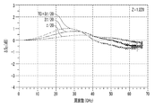
- FIG. 3 is a diagram showing a configuration of an optical modulator of the optical transmitter according to the first embodiment of the present invention. It is a figure which shows the frequency characteristic of an optical transmitter when length of a transmission line is made constant and characteristic impedance is changed. It is a figure which shows the frequency characteristic of an optical transmitter when the characteristic impedance of a transmission line is made constant and the length is changed. It is a figure which shows the frequency characteristic of an optical transmitter when length of a transmission line is made constant and characteristic impedance is changed.
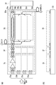
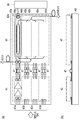
- FIG. 6 is a diagram showing a configuration of an optical modulator of an optical transmitter according to a second embodiment of the present invention. It is a figure which shows the structure of the optical modulator of the optical transmitter concerning Example 3 of this invention.
- FIG. 2 shows the configuration of the optical modulator of the optical transmitter according to the first embodiment of the present invention.
- an optical modulator driver IC 21 connected to a signal source and a semiconductor optical modulator 22 connected to a light source are mounted on a board 23 in a package.
- the semiconductor optical modulator 22 is, for example, a polarization multiplexing quadrature phase modulator (DP-IQ optical modulator), and includes two sets of IQ optical modulators each including two Mach-Zehnder type optical modulators.
- DP-IQ optical modulator polarization multiplexing quadrature phase modulator
- the optical input from the light source is modulated by the applied voltage on which the modulation signal is superimposed in each Mach-Zehnder optical modulator 22a-22d, and multiplexed to output an optical signal (DP-QPSK signal, DP-16QAM signal, etc.). Is output as. Traveling wave electrodes 25a and 25b are used for the Mach-Zehnder optical modulators 22a to 22d, and termination resistors 24a and 24b are connected so that an input signal is not reflected and returned from the terminal end portion of the electrodes. ..
- the driver ICs 21a-21d of the optical modulator driver IC 21 have an open collector type configuration in the case of a bipolar transistor and an open drain type configuration in the case of a FET, and are connected from the power source 26 connected via the terminating resistors 24a, 24b. Electric current is supplied.
- the output reflection characteristic is the total reflection characteristic because there is no sending end resistance. As a result, there is no power consumption due to the sending end resistance and the configuration is such that it is electrically connected directly to the Mach-Zehnder interferometer type optical modulators 22a-22d, so that external components such as the bias T are not required.
- optical modulator driver IC 21 and the semiconductor optical modulator 22 are flip-chip mounted on the substrate 23, and the space between them is connected by the transmission line 27 on the substrate.
- a driver IC having an open collector type or open drain type output format is provided, and the characteristic impedance (Z) of the transmission line connecting the driver IC and the optical modulator is set to the traveling wave type electrode and the termination. It is set higher than the characteristic impedance (Z0) of the optical modulator including the resistance by 20% or more.
- the delay time (TD) due to the transmission line is set to 1/20 or more of the cycle ( ⁇ ) of the electric signal of the target frequency.
- the transmission line 27 between the optical modulator driver IC 21 and the semiconductor optical modulator 22 and the characteristic impedance of the semiconductor optical modulator 22 do not match, a signal at the connection portion between the transmission line 27 and the semiconductor optical modulator 22 is Reflection occurs.
- the output end of the driver IC 21a-21d, which is the other end of the transmission line 27, is an open collector type or an open drain type, the reflection characteristic is total reflection. Therefore, multiple reflection occurs at both ends of the transmission line 27, and the frequency characteristic of the entire optical modulator of the optical transmitter changes.
- Fig. 3 shows the change in frequency characteristics of the optical transmitter when the length of the transmission line is fixed and the characteristic impedance is changed. Specifically, the difference ( ⁇ S21) in the frequency characteristics is shown in comparison with the case where the characteristic impedance of the transmission line 27 and the characteristic impedance of the semiconductor optical modulator 22 are the same. It is expressed by a decibel value, and represents a difference obtained by subtracting the frequency characteristic when the optical modulator driver IC 21 and the semiconductor optical modulator 22 are directly connected from the frequency characteristic when the transmission line 27 connects.
- Z0 represents the characteristic impedance of the semiconductor optical modulator 22, and ⁇ represents the cycle of the electric signal of the target frequency.
- the frequency is 32 GHz and its period is ⁇ .
- FIG. 3 shows that when the characteristic impedance is changed by setting the length of the transmission line 27 to a constant value ⁇ /20
- FIG. 4 shows that the characteristic impedance of the transmission line 27 is set to a constant value 1.2Z0 and the length is changed
- FIG. 5 corresponds to a case where the length of the transmission line 27 is set to a constant value ⁇ /10 and the characteristic impedance is changed. Considering the frequency loss at the time of mounting in the optical transmitter, it is desirable that the frequency characteristics rise near the target frequency of 32 GHz.
- the characteristic impedance of the transmission line 27 is smaller than about 1.2Z0, or when the length of the transmission line 27 is smaller than about ⁇ /20, almost peaking effect can be obtained near the frequency of 32 GHz.
- the length of the transmission line is short, that is, when the delay time is short, the phase hardly rotates at the desired frequency and does not change. On the contrary, if the delay time is too long and the phase rotates more than a half wavelength at a desired wavelength, a standing wave will be generated, so it is necessary to be less than a half wavelength. That is, the length of the transmission line needs to be about ⁇ /2 or less.
- the characteristic impedance (Z) of the transmission line 27 is set to be 20% or more higher than the characteristic impedance (Z0) of the semiconductor optical modulator 22, and the length of the transmission line 27 is set to an electrical value for driving the optical modulator. It is set to 1/20 or more of the electrical length corresponding to the wavelength so that the delay is 1/20 or more of the frequency of the signal (usually corresponding to the required 3 dB band frequency). With such a configuration, the response is improved around the desired frequency, and a constant frequency peaking effect can be obtained.
- the characteristic impedance (Z) between the driver IC and the optical modulator may be set higher than the characteristic impedance (Z0) of the optical modulator, the output line and the output pad portion inside the optical modulator driver IC21 Even if the impedance or the impedance of the input line to the Mach-Zehnder interferometer type optical modulators 22a-22d inside the semiconductor optical modulator 22 or the input pad section is made higher than the characteristic impedance (Z0) of the semiconductor optical modulator 22 by 20% or more. Good. Effectively, it can contribute to the length of the transmission line connecting between the driver IC and the optical modulator, and the same effect as the impedance change of the transmission line can be expected. Moreover, if both are used together, an additional effect can be expected.
- FIG. 6 shows the configuration of the optical modulator of the optical transmitter according to the second embodiment of the present invention.
- an optical modulator driver IC 31 connected to a signal source and a semiconductor optical modulator 32 connected to a light source are mounted on a substrate 33 in the package.
- Traveling wave electrodes 35a and 35b are used for the Mach-Zehnder interferometer type optical modulators 32a to 32d, and terminating resistors 34a and 34b are connected so as to prevent an input signal from being reflected and returned from the end portions of the electrodes. ..
- the driver ICs 31a to 31d of the optical modulator driver IC 31 have an open collector type or open drain type configuration, and a current is supplied from a power supply 36 connected via terminating resistors 34a and 34b.
- the optical modulator driver IC 31 and the semiconductor optical modulator 32 are flip-chip mounted on the substrate 33, and like the first embodiment, a line substrate 37 on which a transmission line having a desired impedance is formed is used to connect them. Connected.
- the transmission line can not only be created linearly, but can also be a curved line to increase the distance in the same area. Further, by mounting the line board 37 by flip chip, it is possible to select and mount a line board having a desired impedance from the line boards having different impedances. Further, in order to suppress interference with the outside such as other channels, a part of the transmission line can be an inner layer line of a package made of a multilayer ceramic substrate, and at this time, it can also be a curved line.
- FIG. 7 shows the configuration of the optical modulator of the optical transmitter according to the third embodiment of the present invention.
- an optical modulator driver IC 41 connected to a signal source and a semiconductor optical modulator 42 connected to a light source are mounted on a board 43 in a package.
- Traveling-wave electrodes 45a and 45b are used for the Mach-Zehnder optical modulators 42a to 42d, and terminating resistors 44a and 44b are connected so that an input signal is not reflected and returned from the terminal ends of the electrodes. ..
- the driver ICs 41a-41d of the optical modulator driver IC 41 have an open collector type or open drain type configuration, and a current is supplied from a power source 46 connected via terminating resistors 44a and 44b.
- the optical modulator driver IC 41 and the semiconductor optical modulator 42 are connected by a bonding wire 47 that connects the pads formed on the substrate 43, and forms a transmission line having a desired impedance as in the first embodiment. ing.
- a desired impedance can be set by changing the thickness, length, and number of bonding wires.
- the driver IC of Example 1-3 is an open collector type or an open drain type. However, the output is such that multiple reflection occurs between the output end of the driver IC and the connection between the transmission line and the semiconductor optical modulator.
- the impedance should be high. Specifically, the output impedance of the driver IC may be three times or more higher than the characteristic impedance of the optical modulator.
- the response is improved around the desired frequency, and a constant frequency peaking effect can be obtained.
- the conventional optical modulator driver IC and the semiconductor optical modulator are applied, the frequency characteristic of the optical transmitter can be improved.
Landscapes
- Physics & Mathematics (AREA)
- Nonlinear Science (AREA)
- Optics & Photonics (AREA)
- General Physics & Mathematics (AREA)
- Electromagnetism (AREA)
- Engineering & Computer Science (AREA)
- Computer Networks & Wireless Communication (AREA)
- Signal Processing (AREA)
- Optical Modulation, Optical Deflection, Nonlinear Optics, Optical Demodulation, Optical Logic Elements (AREA)
- Optical Communication System (AREA)
Abstract
光送信機を構成する部品によって帯域を制御することにより、周波数特性を向上させた光送信機を提供する。進行波型電極および終端抵抗を含む光変調器と、前記光変調器を駆動する光変調器ドライバとを備えた光送信機において、前記光変調器ドライバと前記光変調器とを接続する伝送線路の特性インピーダンスは、前記光変調器の特性インピーダンスより20%以上高く、前記伝送線路の電気長は、前記光変調器を駆動する電気信号の3dB帯域周波数に相当する波長の1/20以上1/2以下である。
Description
本発明は、光送信機に関し、より詳細には、ディジタルコヒーレント通信に用いられ、光変調器と、光変調器を駆動するドライバとを備えた光送信機に関する。
近年、5G移動体通信、VOD(Video On Demand)など、様々なサービスの必要とする総通信容量は増大の一途を辿り、基幹となる光通信回線にも不断の増大が求められている。これに伴い、数百km以上の長距離の都市間を結ぶ基幹回線ばかりでなく、100km未満の都市間、データセンタ間を結ぶ比較的近距離の回線においても、大容量の通信装置が必要とされている。従来、数千kmに及ぶ基幹回線のみに用いられてきたディジタルコヒーレント通信技術は、大きな通信容量に加えて、分散耐力、高い受信感度などの優れた特性のため、100km前後の比較的短い距離の通信にも使われるようになってきている。通信網は、末端になるほど細かく分かれているため、これらの距離で用いられる通信機器の数は基幹回線の場合に比べてはるかに多い。このため、通信機器に対するサイズの小型化、コスト低減の要求は、長距離用の通信機器と比較すると、ずっと厳しいものになる。
ディジタルコヒーレント通信に用いられる光送信機において、従来、高性能なニオブ酸リチウム(LN)変調器が用いられてきた。さらに、上記のような小型化のために、最近では半導体光変調器が用いられている。半導体材料としては、インジウム燐(InP)が小型高性能化には適しているが、光回路の小型化・集積化には、シリコンフォトニクス技術を利用したシリコン光変調器も用いられる。
通信機器の小型化が進展する一方、近年、信号伝送ボーレートの高速化が進み、32Gbaudから64Gbaudにまで届こうとしている。伝送する周波数レートが高くなるにつれ、光送信機を構成する部品に対する高周波特性への要求も厳しくなっている。
図1に、従来のコヒーレント光送信機の光変調部の構成を示す。光送信機は、信号源に接続された光変調器ドライバIC11と、光源に接続された半導体光変調器12とが、パッケージ内の基板13上に実装されている。半導体光変調器12は、一例として、偏波多重直交位相変調器(DP-IQ光変調器)であり、マッハツェンダ型光変調器2つからなるIQ光変調器を2組備えている。マッハツェンダ型光変調器12a-12dの2本のアーム導波路のpn接合部に電圧を印加することにより、ポッケルス効果、キャリアプラズマ効果等の半導体の電気光学効果により屈折率を変化させる。光源からの光入力は、各々のマッハツェンダ型光変調器12a-12dにおいて、変調信号が重畳された印加電圧による電気光学効果によって変調され、合波されて光信号出力(DP-QPSK信号、DP-16QAM信号等)として出力される。
半導体光変調器12において、十分な電気光学効果を得るために必要な電気信号振幅が大きいので、十分な振幅を得るため、電気入力信号を増幅するために光変調器ドライバIC11を用いている。光変調器ドライバIC11のドライバIC11a-11dの構成としては、非特許文献1に記載されているように様々な形式がある。コンパクトに構成するためには、バイポーラトランジスタの場合ならばオープンコレクタ型、FETの場合ならばオープンドレイン型の構成が有用である。オープンコレクタ型の構成では、ドライバIC11a-11dが送端抵抗を内蔵していないために消費電力が低い。また、ドライバIC11a-11dとマッハツェンダ型光変調器12a-12dとを直結して用いることができ、DC分離のためのバイアスTのような外部部品が不要になり、小型・安価に構成できる利点がある。
マッハツェンダ型光変調器12a-12dとしては、進行波型電極15a,15bがよく用いられる。この光変調器では、光と電気信号を同じ方向に伝搬させることにより十分な変調効率を得ることができる。進行波型電極15a,15bの構成では、マッハツェンダ型光変調器12a-12dに入力した電気信号が電極の終端部から反射して戻ってこないように、ドライバIC11a-11dの接続端とは反対側に終端抵抗14a,14bが接続される。終端抵抗14a,14bは、進行波型電極15a,15bの線路としての特性インピーダンスと概ね一致するように設計され、ドライバIC11a-11dから見たマッハツェンダ型光変調器12a-12dの電気反射減衰量は、終端抵抗14a,14bの抵抗値が特性インピーダンスと一致した場合に最大となる。
光送信機の実装形態については、特に大幅な小型化を実現するために、非特許文献2に記載されているようなフリップチップ構成がよく用いられる。この方法は、半導体チップの各電極パッドに金属ボールをつけたまま裏向きに実装するため、ボンディングの場合のように、半導体チップの周りに広い領域が不要になる。また、上面からの放熱が容易になるため、半導体チップを実装したパッケージ全体を、リードレスで小型化に優れたボールグリッドアレイ(BGA)実装することが容易になる利点がある。
N. Wolf, L. Yan, J.-H. Choi, T. Kapa, S. Wunsch, R. Klotzer, K.-O. Vethaus, H.-G. Bach, M. Schell, "Electro-Optic Co-Design to Minimize Power Consumption of a 32GBd Optical IQ-Transmitter Using InP MZ-Modulators", 2015 IEEE Compound Semiconductor Integrated Circuit Symposium (CSICS), pp. 117-120, 2015.
S. Kanazawa, T. Fujisawa, K. Takahata1, Y. Nakanishi1, H. Yamazaki, Y. Ueda, W. Kobayashi, Y. Muramoto, H. Ishii, and H. Sanjoh, "56-Gbaud 4-PAM operation of flip-chip interconnection lumped-electrode EADFB laser module for equalizer-free transmission", OFC2016, W4J.1, 2016.
図1に示した光送信機のように、光変調器ドライバIC11と半導体光変調器12とをボンディングによる実装に代えてフリップチップ実装する場合は、光変調器ドライバIC11と半導体光変調器12との間を基板上の線路で接続することになる。上述したように、光変調器ドライバIC11から見た半導体光変調器12の電気反射減衰量を最大とするためには、基板上の線路についても、進行波型電極15a,15bの特性インピーダンスと一致するように設計すればよい。
ボンディング接続の場合であってもフリップチップ実装の場合であっても、64Gbaudなどの高いボーレートの送信機が必要になる400G送受信機を構成する場合、従来の光変調器ドライバIC11と半導体光変調器12とを単純に接続する方法では帯域が不足する場合があった。周波数特性が低いと、信号全体のパワースペクトルが減衰し、送信光強度までも低くなって送受信機のダイナミックレンジまで低下してしまうという問題があった。
本発明の目的は、光送信機を構成する部品によって帯域を制御することにより、周波数特性を向上させた光送信機を提供することにある。
本発明は、このような目的を達成するために、一実施態様は、進行波型電極および終端抵抗を含む光変調器と、前記光変調器を駆動する光変調器ドライバとを備えた光送信機において、前記光変調器ドライバと前記光変調器とを接続する伝送線路の特性インピーダンスは、前記光変調器の特性インピーダンスより20%以上高く、前記伝送線路の電気長は、前記光変調器を駆動する電気信号の3dB帯域周波数に相当する波長の1/20以上1/2以下であることを特徴とする。
本発明によれば、所望の周波数の周辺で応答が改善し、一定の周波数ピーキング効果が得られ、周波数特性を改善することができる。
以下、図面を参照しながら本発明の実施形態について詳細に説明する。
図2に、本発明の実施例1にかかる光送信機の光変調部の構成を示す。光送信機は、信号源に接続された光変調器ドライバIC21と、光源に接続された半導体光変調器22とが、パッケージ内の基板23上に実装されている。半導体光変調器22は、一例として、偏波多重直交位相変調器(DP-IQ光変調器)であり、マッハツェンダ型光変調器2つからなるIQ光変調器を2組備えている。光源からの光入力は、各々のマッハツェンダ型光変調器22a-22dにおいて、変調信号が重畳された印加電圧により変調され、合波されて光信号出力(DP-QPSK信号、DP-16QAM信号等)として出力される。マッハツェンダ型光変調器22a-22dには、進行波型電極25a,25bが用いられ、入力した信号が電極の終端部から反射して戻ってこないように、終端抵抗24a,24bが接続されている。
光変調器ドライバIC21のドライバIC21a-21dは、バイポーラトランジスタの場合ならばオープンコレクタ型、FETの場合ならばオープンドレイン型の構成を有し、終端抵抗24a,24bを介して接続された電源26から電流が供給される。オープンコレクタ型またはオープンドレイン型の場合、送端抵抗がないため出力反射特性が全反射特性となっている。これにより送端抵抗による消費電力がなく、マッハツェンダ型光変調器22a-22dと電気的に直結する構成をとっているため、バイアスTのような外部部品が不要になる。
光変調器ドライバIC21と半導体光変調器22とは、基板23上にフリップチップ実装されており、その間を基板上の伝送線路27で接続されている。
実施例1においては、オープンコレクタ型またはオープンドレイン型の出力形式を有するドライバICを備え、ドライバICと光変調器との間を結ぶ伝送線路の特性インピーダンス(Z)を、進行波型電極および終端抵抗を含む光変調器の特性インピーダンス(Z0)よりも20%以上高く設定する。加えて、伝送線路による遅延時間(TD)を目的とする周波数の電気信号の周期(τ)の1/20以上とする。以下、実施例1の構成について詳細に説明する。
光変調器ドライバIC21から半導体光変調器22までの間の伝送線路27と、半導体光変調器22の特性インピーダンスとが合致しないため、伝送線路27と半導体光変調器22との接続部において信号の反射が起きる。一方、伝送線路27の他端であるドライバIC21a-21dの出力端は、オープンコレクタ型またはオープンドレイン型なので反射特性は全反射である。従って、伝送線路27の両端で多重反射が起き、光送信機の光変調部全体の周波数特性が変化する。
図3に、伝送線路の長さを一定にし、特性インピーダンスを変化させたときの光送信機の周波数特性の変化を示す。具体的には、伝送線路27の特性インピーダンスと半導体光変調器22の特性インピーダンスとが一致している場合と比較した周波数特性の差分(ΔS21)を示している。デシベル値で表し、伝送線路27により接続した場合の周波数特性から、光変調器ドライバIC21と半導体光変調器22とを直結した場合の周波数特性を差し引いた差分を表している。Z0は、半導体光変調器22の特性インピーダンスを表し、τは、目的とする周波数の電気信号の周期を表す。図3においては、周波数を32GHzとし、その周期をτとしている。
図3は、伝送線路27の長さを一定値τ/20にして特性インピーダンスを変化させた場合、同様に、図4は、伝送線路27の特性インピーダンスを一定値1.2Z0にして長さを変化させた場合、図5は、伝送線路27の長さを一定値τ/10にして特性インピーダンスを変化させた場合に相当する。光送信機への実装時の周波数損失を考えると、目的とする周波数32GHz近辺で、周波数特性が持ち上がっていることが望ましい。
図3-5を参照すると、伝送線路27の特性インピーダンスが1.2Z0程度より小さい場合、または伝送線路27の長さがτ/20程度より小さい場合、周波数32GHz近辺で、殆どピーキングの効果が得られないことがわかる。これは、インピーダンス変化が小さすぎる場合は、インピーダンス変化部での反射が殆ど発生せず多重反射の寄与が小さくなるためである。また、伝送線路の長さが短い場合、すなわち遅延時間が小さい場合は、所望の周波数で殆ど位相が回らず変化しないためである。逆に、遅延時間が長すぎて所望の波長で位相が半波長以上回ると定在波がたってしまうため、半波長以下であることが必要になる。つまり、伝送線路の長さはτ/2程度以下である必要がある。
以上のことから、伝送線路27の特性インピーダンス(Z)を、半導体光変調器22の特性インピーダンス(Z0)よりも20%以上高くし、伝送線路27の長さを、光変調器を駆動する電気信号の周波数(通常は必要な3dB帯域周波数に相当する)の1/20以上の遅延となるように、波長に相当する電気長の1/20以上とする。このような構成により、所望の周波数の周辺で応答が改善し、一定の周波数ピーキング効果が得られるようになる。
なお、ドライバICと光変調器との間の特性インピーダンス(Z)を、光変調器の特性インピーダンス(Z0)よりも高くすればよいので、光変調器ドライバIC21内部の出力線路、出力パッド部のインピーダンス、または半導体光変調器22内部のマッハツェンダ型光変調器22a-22dへの入力線路、入力パッド部のインピーダンスを、半導体光変調器22の特性インピーダンス(Z0)よりも20%以上高くしてもよい。実効的には、ドライバICと光変調器との間を結ぶ伝送線路の長さに寄与させることができ、伝送線路のインピーダンス変化と同様の効果が期待できる。また、両者を併用すれば、付加的な効果が期待できる。
図6に、本発明の実施例2にかかる光送信機の光変調部の構成を示す。光送信機は、信号源に接続された光変調器ドライバIC31と、光源に接続された半導体光変調器32とが、パッケージ内の基板33上に実装されている。マッハツェンダ型光変調器32a-32dには、進行波型電極35a,35bが用いられ、入力した信号が電極の終端部から反射して戻ってこないように、終端抵抗34a,34bが接続されている。
光変調器ドライバIC31のドライバIC31a-31dは、オープンコレクタ型またはオープンドレイン型の構成を有し、終端抵抗34a,34bを介して接続された電源36から電流が供給される。光変調器ドライバIC31と半導体光変調器32とは、基板33上にフリップチップ実装されており、実施例1と同様に、所望のインピーダンスを有する伝送線路が形成された線路基板37により、両者を接続している。
所望のインピーダンスに設定するために、伝送線路は、直線的に作成するばかりでなく、同じ面積で距離を長くするために曲り線路にすることができる。また、線路基板37をフリップチップで実装することにより、インピーダンスの異なる線路基板の中から所望のインピーダンスの線路基板を選択して実装することもできる。さらに、他のチャネルなど外部との干渉を抑圧するため、伝送線路の一部を多層セラミック基板で作成したパッケージの内層線路にすることもでき、このときにも、曲がり線路にすることもできる。
図7に、本発明の実施例3にかかる光送信機の光変調部の構成を示す。光送信機は、信号源に接続された光変調器ドライバIC41と、光源に接続された半導体光変調器42とが、パッケージ内の基板43上に実装されている。マッハツェンダ型光変調器42a-42dには、進行波型電極45a,45bが用いられ、入力した信号が電極の終端部から反射して戻ってこないように、終端抵抗44a,44bが接続されている。
光変調器ドライバIC41のドライバIC41a-41dは、オープンコレクタ型またはオープンドレイン型の構成を有し、終端抵抗44a,44bを介して接続された電源46から電流が供給される。光変調器ドライバIC41と半導体光変調器42とは、基板43上に形成されたパッド間を接続するボンディングワイヤ47により接続され、実施例1と同様に、所望のインピーダンスを有する伝送線路を形成している。ボンディングワイヤの太さ、長さ、本数を変えることにより、所望のインピーダンスに設定することができる。
実施例1-3のドライバICは、オープンコレクタ型またはオープンドレイン型としたが、ドライバICの出力端と、伝送線路と半導体光変調器の接続部との間で多重反射が起きる程度に、出力インピーダンスが高ければよい。具体的には、ドライバICの出力インピーダンスは、光変調器の特性インピーダンスより3倍以上高ければよい。
本実施形態によれば、光送信機を構成する部品によって帯域を制御することにより、所望の周波数の周辺で応答が改善し、一定の周波数ピーキング効果が得られるようになる。これにより、従来の光変調器ドライバICと半導体光変調器とを適用した場合であっても、光送信機の周波数特性を向上させることができる。
11,21,31,41 光変調器ドライバIC
12,22,32,42 半導体光変調器
13,23,33,43 基板
14,24,34,44 終端抵抗
15,25,35,45 進行波型電極
26,36,46 電源
27 伝送線路
37 線路基板
47 ボンディングワイヤ
12,22,32,42 半導体光変調器
13,23,33,43 基板
14,24,34,44 終端抵抗
15,25,35,45 進行波型電極
26,36,46 電源
27 伝送線路
37 線路基板
47 ボンディングワイヤ
Claims (6)
- 進行波型電極および終端抵抗を含む光変調器と、前記光変調器を駆動する光変調器ドライバとを備えた光送信機において、
前記光変調器ドライバと前記光変調器とを接続する伝送線路の特性インピーダンスは、前記光変調器の特性インピーダンスより20%以上高く、前記伝送線路の電気長は、前記光変調器を駆動する電気信号の3dB帯域周波数に相当する波長の1/20以上1/2以下であることを特徴とする光送信機。 - 前記光変調器ドライバの出力インピーダンスは、前記光変調器の特性インピーダンスより3倍以上高いことを特徴とする請求項1に記載の光送信機。
- 前記光変調器ドライバの出力は、オープンコレクタ型またはオープンドレイン型であることを特徴とする請求項2に記載の光送信機。
- 前記光変調器ドライバの出力線路、出力パッド部、前記光変調器の入力線路、または入力パッド部のインピーダンスを、前記光変調器の特性インピーダンスより高くしたことを特徴とする請求項1、2または3に記載の光送信機。
- 前記光変調器と前記光変調器ドライバとは、基板上にフリップチップ実装されており、前記伝送線路は、前記基板上にフリップチップ実装された線路基板に形成されていることを特徴とする請求項1ないし4のいずれか1項に記載の光送信機。
- 前記光変調器と前記光変調器ドライバとは、基板上にフリップチップ実装されており、前記伝送線路は、前記基板上に形成されたパッド間を接続するボンディングワイヤであることを特徴とする請求項1ないし4のいずれか1項に記載の光送信機。
Priority Applications (1)
| Application Number | Priority Date | Filing Date | Title |
|---|---|---|---|
| US17/294,980 US11340478B2 (en) | 2018-12-11 | 2019-12-05 | Optical transmitter |
Applications Claiming Priority (2)
| Application Number | Priority Date | Filing Date | Title |
|---|---|---|---|
| JP2018231859A JP7095583B2 (ja) | 2018-12-11 | 2018-12-11 | 光送信機 |
| JP2018-231859 | 2018-12-11 |
Publications (1)
| Publication Number | Publication Date |
|---|---|
| WO2020121928A1 true WO2020121928A1 (ja) | 2020-06-18 |
Family
ID=71076842
Family Applications (1)
| Application Number | Title | Priority Date | Filing Date |
|---|---|---|---|
| PCT/JP2019/047536 Ceased WO2020121928A1 (ja) | 2018-12-11 | 2019-12-05 | 光送信機 |
Country Status (3)
| Country | Link |
|---|---|
| US (1) | US11340478B2 (ja) |
| JP (1) | JP7095583B2 (ja) |
| WO (1) | WO2020121928A1 (ja) |
Cited By (1)
| Publication number | Priority date | Publication date | Assignee | Title |
|---|---|---|---|---|
| CN116097157A (zh) * | 2020-07-29 | 2023-05-09 | 日本电信电话株式会社 | 半导体光调制器 |
Families Citing this family (7)
| Publication number | Priority date | Publication date | Assignee | Title |
|---|---|---|---|---|
| JP7131425B2 (ja) * | 2019-02-19 | 2022-09-06 | 日本電信電話株式会社 | 光変調器 |
| WO2024075172A1 (ja) * | 2022-10-03 | 2024-04-11 | 日本電信電話株式会社 | 光送信器 |
| WO2024075168A1 (ja) * | 2022-10-03 | 2024-04-11 | 日本電信電話株式会社 | 光送信器 |
| WO2024075171A1 (ja) * | 2022-10-03 | 2024-04-11 | 日本電信電話株式会社 | 光送信器 |
| JPWO2024075166A1 (ja) * | 2022-10-03 | 2024-04-11 | ||
| TWI881329B (zh) * | 2023-04-25 | 2025-04-21 | 緯創資通股份有限公司 | 光發射器及光子積體電路 |
| US20250047061A1 (en) * | 2023-07-31 | 2025-02-06 | Maxlinear, Inc. | Co-packaged photonics driver |
Citations (3)
| Publication number | Priority date | Publication date | Assignee | Title |
|---|---|---|---|---|
| US20080285978A1 (en) * | 2007-05-14 | 2008-11-20 | Electronics And Telecommunications Research Institute | Optical hybrid module |
| JP2016537691A (ja) * | 2013-11-25 | 2016-12-01 | フラウンホファー‐ゲゼルシャフト・ツア・フェルデルング・デア・アンゲヴァンテン・フォルシュング・エー・ファウ | 電気光学変調器装置 |
| JP2018092100A (ja) * | 2016-12-07 | 2018-06-14 | 日本電信電話株式会社 | 光送信器 |
Family Cites Families (6)
| Publication number | Priority date | Publication date | Assignee | Title |
|---|---|---|---|---|
| JP3438443B2 (ja) * | 1995-11-10 | 2003-08-18 | Kddi株式会社 | 光デバイス |
| JP3936256B2 (ja) * | 2002-07-18 | 2007-06-27 | 富士通株式会社 | 光半導体装置 |
| KR20060059863A (ko) * | 2004-03-18 | 2006-06-02 | 니폰덴신뎅와 가부시키가이샤 | 광변조기 및 광변조 방법 |
| US7011458B2 (en) * | 2004-07-12 | 2006-03-14 | Opnext Japan, Inc. | Optical module |
| JP2019159115A (ja) * | 2018-03-13 | 2019-09-19 | 日本電信電話株式会社 | 光変調器 |
| JP7192875B2 (ja) * | 2018-10-30 | 2022-12-20 | 日本電気株式会社 | 光送信器、光送信システム及び光送信方法 |
-
2018
- 2018-12-11 JP JP2018231859A patent/JP7095583B2/ja active Active
-
2019
- 2019-12-05 US US17/294,980 patent/US11340478B2/en active Active
- 2019-12-05 WO PCT/JP2019/047536 patent/WO2020121928A1/ja not_active Ceased
Patent Citations (3)
| Publication number | Priority date | Publication date | Assignee | Title |
|---|---|---|---|---|
| US20080285978A1 (en) * | 2007-05-14 | 2008-11-20 | Electronics And Telecommunications Research Institute | Optical hybrid module |
| JP2016537691A (ja) * | 2013-11-25 | 2016-12-01 | フラウンホファー‐ゲゼルシャフト・ツア・フェルデルング・デア・アンゲヴァンテン・フォルシュング・エー・ファウ | 電気光学変調器装置 |
| JP2018092100A (ja) * | 2016-12-07 | 2018-06-14 | 日本電信電話株式会社 | 光送信器 |
Non-Patent Citations (2)
| Title |
|---|
| KANAZAWA ET AL.: "56-Gbaud 4-PAM operation of flip- chip interconnection lumped-electrode EADFB laser module for equalizer-free transmission", 2016 OPTICAL FIBER COMMUNICATIONS CONFERENCE AND EXHIBITION (OFC), 20 March 2016 (2016-03-20), XP032942900 * |
| ZHU, K. H. ET AL.: "Modeling and optimization of the bond-wire interface in a hybrid CMOS-photonic traveling-wave MZM transmitter", SYSTEM-ON-CHIP CONFERENCE (SOCC) , 2016 IEEE INTERNATIONAL, 6 September 2016 (2016-09-06), pages 151 - 155, XP033086782 * |
Cited By (4)
| Publication number | Priority date | Publication date | Assignee | Title |
|---|---|---|---|---|
| CN116097157A (zh) * | 2020-07-29 | 2023-05-09 | 日本电信电话株式会社 | 半导体光调制器 |
| EP4191325A4 (en) * | 2020-07-29 | 2024-03-27 | Nippon Telegraph And Telephone Corporation | OPTICAL SEMICONDUCTOR MODULATOR |
| US12393064B2 (en) | 2020-07-29 | 2025-08-19 | Nippon Telegraph And Telephone Corporation | Semiconductor optical modulator |
| CN116097157B (zh) * | 2020-07-29 | 2025-09-19 | 日本电信电话株式会社 | 半导体光调制器 |
Also Published As
| Publication number | Publication date |
|---|---|
| JP2020095122A (ja) | 2020-06-18 |
| JP7095583B2 (ja) | 2022-07-05 |
| US11340478B2 (en) | 2022-05-24 |
| US20220011606A1 (en) | 2022-01-13 |
Similar Documents
| Publication | Publication Date | Title |
|---|---|---|
| JP7095583B2 (ja) | 光送信機 | |
| US12321025B2 (en) | Integrated silicon photonics transceivers enabling ultra-high-speed high dense input/output and interconnect for Terabyte per second optical interconnect | |
| JP7335539B2 (ja) | 高速光送受信装置 | |
| US10866439B2 (en) | High-frequency transmission line and optical circuit | |
| JP7133405B2 (ja) | 半導体装置 | |
| JP6497980B2 (ja) | 光送信モジュール及び光送受信モジュール | |
| JPH11231173A (ja) | 高速動作可能な光デバイス | |
| WO2003005101A1 (en) | Modified optical modulation system | |
| CN114079511A (zh) | 与微环调制器耦合的端接电路以减少信号反射 | |
| JP7249745B2 (ja) | 光サブアッセンブリ及び光モジュール | |
| JP2017134241A (ja) | 光変調器及びそれを用いた光送信装置 | |
| JP7468279B2 (ja) | 光変調器とそれを用いた光送信装置 | |
| US11467467B2 (en) | Optical modulator | |
| JP7263966B2 (ja) | 光デバイス | |
| CN110007490B (zh) | 光调制器及使用了该光调制器的光发送装置 | |
| US20090003844A1 (en) | High speed optoelectronic receiver | |
| US20250383577A1 (en) | Optical device and optical transmission apparatus using the same | |
| JP7710143B2 (ja) | 光回路 | |
| JP7098930B2 (ja) | 光変調器及びそれを用いた光送信装置 | |
| JP6288879B2 (ja) | 高周波半導体モジュール | |
| JP7388021B2 (ja) | 光デバイス | |
| JP2002350792A (ja) | Ea変調器モジュール | |
| JP7687421B2 (ja) | 光変調器 | |
| WO2023105641A1 (ja) | 光回路 | |
| JP2019033380A (ja) | 終端回路および終端回路を構成する配線板 |
Legal Events
| Date | Code | Title | Description |
|---|---|---|---|
| 121 | Ep: the epo has been informed by wipo that ep was designated in this application |
Ref document number: 19897310 Country of ref document: EP Kind code of ref document: A1 |
|
| NENP | Non-entry into the national phase |
Ref country code: DE |
|
| 122 | Ep: pct application non-entry in european phase |
Ref document number: 19897310 Country of ref document: EP Kind code of ref document: A1 |